Embed Size (px)
Citation preview
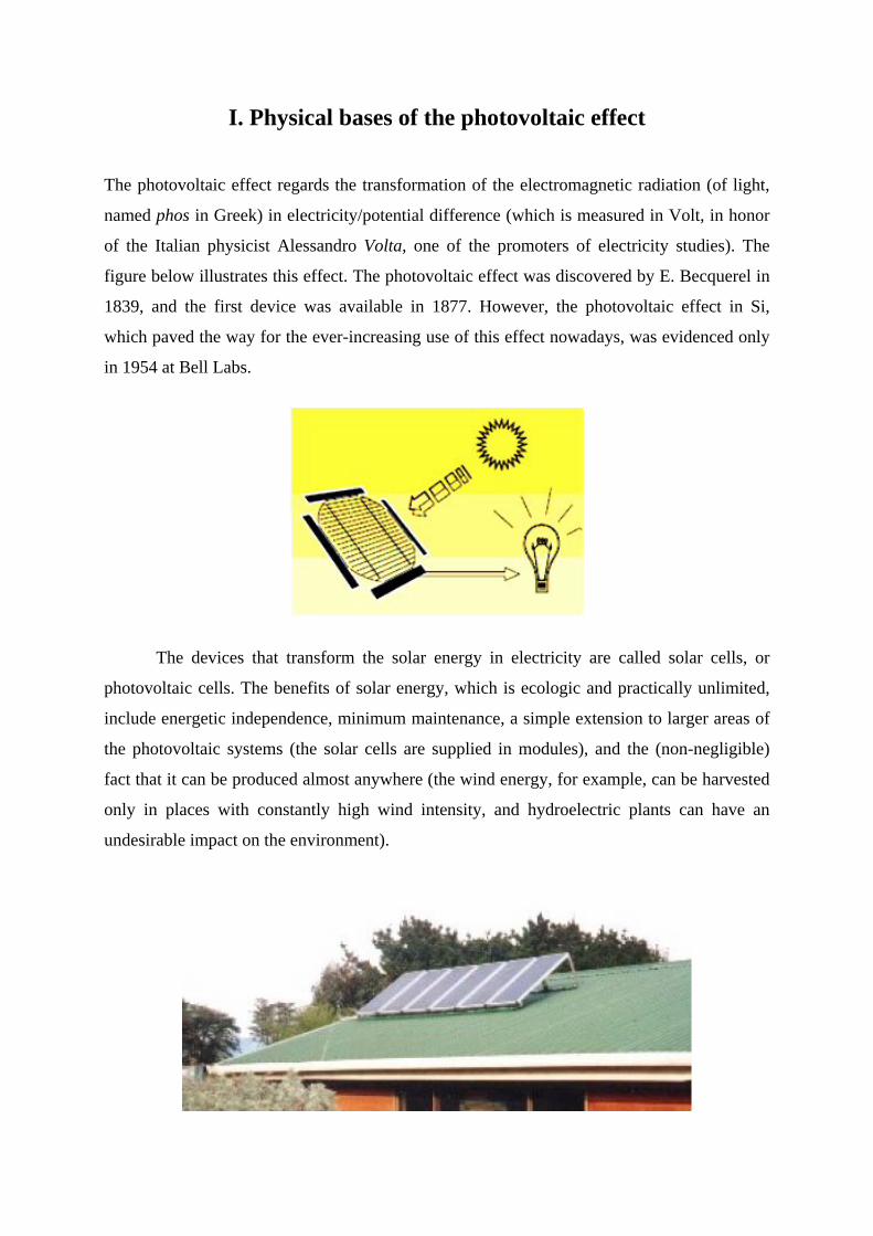
I. Physical bases of the photovoltaic effect
The photovoltaic effect regards the transformation of the electromagnetic radiation (of light,
named phos in Greek) in electricity/potential difference (which is measured in Volt, in honor
of the Italian physicist Alessandro Volta, one of the promoters of electricity studies). The
figure below illustrates this effect. The photovoltaic effect was discovered by E. Becquerel in
1839, and the first device was available in 1877. However, the photovoltaic effect in Si,
which paved the way for the ever-increasing use of this effect nowadays, was evidenced only
in 1954 at Bell Labs.
The devices that transform the solar energy in electricity are called solar cells, or
photovoltaic cells. The benefits of solar energy, which is ecologic and practically unlimited,
include energetic independence, minimum maintenance, a simple extension to larger areas of
the photovoltaic systems (the solar cells are supplied in modules), and the (non-negligible)
fact that it can be produced almost anywhere (the wind energy, for example, can be harvested
only in places with constantly high wind intensity, and hydroelectric plants can have an
undesirable impact on the environment).

2
An example of 6 modules connected in parallel, each consisting of 40 photovoltaic cells
connected in series, is presented in the figure above. This solar panel can be used for battery
recharging and/or for powering domestic appliances with 12 V dc.
To understand the operation of solar cells, one needs to know that
1) The solar radiation is composed of photons with a wide energy distribution. The photon
energy ωh=E depends on the frequency ω or on the wavelength == k/2πλ ωπ /2 c of the
electromagnetic radiation as follows: the energy decreases as λ increases. The energetic
distribution of the flux of photons emitted by the Sun is represented in the figure below.
Please note that the solar photon flux extends on a much wider energetic interval than the
visible range, and has a maximum in the infrared spectral region.
2) The photons interact with the atoms of a semiconducting material (for example), i.e. are
absorbed, and, if the photon energy is high enough, it can break the bond between the valence
electron and atom. As a result, the valence electron is excited on higher energy levels, so that
a negatively charged conduction electron and a positively charged hole in the valence band
appear simultaneously. These charges move freely in the crystal, until they recombine. The
electron and the hole are the constituents of electricity. For example, the energy necessary for
an electron in the valence band to reach the conduction band of Si corresponds to a
wavelength of 1.12 μm (in infrared!), 70% of photons in the solar radiation being able to
excite an electron in the conduction band of silicon (see the figure below). If the photon
energy is much higher than that corresponding to λ = 1.12 μm, the excess energy is
transformed into heat, which degrades the performance of solar cells.

3
3) To have efficient solar cells, it is necessary to collect the electron-hole pair before
recombination. This can be done by the separation of electrons and holes by a built-in electric
field, the current produced by the electrons and holes generated by photon absorption being
called photocurrent.
For a quantitative treatment of the photovoltaic effect we study in the first part of this
course the formation of energy bands in solids, which determines the classification of
materials in metals, semiconductors and isolators, the doping process of semiconductors, the
junctions between differently-doped semiconductors and, respectively, the heterojunctions
between different materials, the absorption of light and, finally, the photovoltaic effect.
Electron dynamics in crystalline solids Crystal structure The properties of crystalline solids, especially the electron dynamics, are determined by the
symmetry of the crystalline lattice. The crystal lattice is a periodic arrangement of atoms over
large distances, of at least thousands of periods. The materials used in the fabrication of solar
cells include also non-crystalline materials, which have no long-range order, but their optical
properties (in particular, the absorption) are similar to that of crystalline materials because the
wavelength of the incident photons (of the order of 1 μm) is much larger than the
inhomogeneities of the material, so that the photons “see” an effective homogeneous medium.
The macroscopic, perfect crystal is formed by adding identical building blocks (unit
cells) consisting of atoms or groups of atoms. A unit cell is the smallest component that
reproduces the whole crystal by translational repetition along three directions in space. The
periodicity of the resulting crystalline structure is confirmed by X-ray diffraction experiments.

4
A crystal is a combination of a basis and a lattice. The basis is the group of atoms or
molecules that forms, by infinite repetition, the macroscopic crystal, while the lattice (also
called Bravais lattice) is a set of mathematical/abstract points in which the basis is positioned.
(a) (b) Examples of crystals in which the basis consists of (a) one atom and (b) two atoms
In three dimensions, all Bravais lattice points can be obtained as superposition of
integral multiples of two non-planar primitive translation vectors , and : 1a 2a 3a
321 aaaR pnmmnp ++= (1)
(m, n, and p are arbitrary integers). If the basis consists of n atoms, their positions can be
described by the set of vectors 321 aaar jjjj pnm ++= , j = 1,2,…,n, defined with respect to
one point of the Bravais lattice. In general, 1,,0 ≤≤ jjj pnm . The volume of the primitive
unit cell, constructed starting with the primitive translation vectors, is 321 )( aaa ⋅×=Ω . The
primitive unit cell is the unit cell with the smallest volume.
Every point of a Bravais lattice is equivalent to every other point, the Bravais lattice
being invariant under the operation of discrete translation 321 aaaT srqqrs ++= along integer
multiples q, r and s of the primitive translation vectors because =+= mnpqrsmnpqrs RTRT )(
is also a Bravais lattice point. Besides discrete translations, the Bravais lattice is
invariant to the point group operations, which are applied around a point of the lattice that
remains unchanged. These operations are: a) the rotations by an angle
psnrmq +++ ,,R
nC n/2π , n = 1, 2, 3,
4 and 6, about a specific axis, b) the inversion I, which is defined by the operation rr −→ if
applied about the origin, c) the reflection jσ , which can be applied around the horizontal (j =
h), vertical (j = v), or diagonal planes (j = d), and d) the improper rotation , which consists
of the rotation followed by reflection in the plane normal to the rotation axis.
nS
nC
5
(a) (b)
(c)
(d)
(e) Examples of symmetry operations: (a) translations, (b) rotation, (c) inversion, and reflection with respect to (d) a vertical plane, and (e) a horizontal plane.
C2 C3 C4 C6
Examples of two-dimensional figures with different rotation symmetries with respect to an axis normal to their plane.
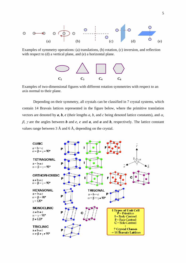
Depending on their symmetry, all crystals can be classified in 7 crystal systems, which
contain 14 Bravais lattices represented in the figure below, where the primitive translation
vectors are denoted by a, b, c (their lengths a, b, and c being denoted lattice constants), and α,
β, γ are the angles between b and c, c and a, and a and b, respectively. The lattice constant
values range between 3 Å and 6 Å, depending on the crystal.
6
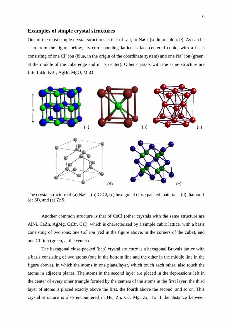
Examples of simple crystal structures One of the most simple crystal structures is that of salt, or NaCl (sodium chloride). As can be
seen from the figure below, its corresponding lattice is face-centered cubic, with a basis
consisting of one Cl− ion (blue, in the origin of the coordinate system) and one Na+ ion (green,
at the middle of the cube edge and in its center). Other crystals with the same structure are
LiF, LiBr, KBr, AgBr, MgO, MnO.
(a) (b) (c)
(d) (e) The crystal structure of (a) NaCl, (b) CsCl, (c) hexagonal close packed materials, (d) diamond (or Si), and (e) ZnS. Another common structure is that of CsCl (other crystals with the same structure are
AlNi, CaZn, AgMg, CsBr, CsI), which is characterized by a simple cubic lattice, with a basis
consisting of two ions: one Cs+ ion (red in the figure above, in the corners of the cube), and
one Cl− ion (green, at the center).
The hexagonal close-packed (hcp) crystal structure is a hexagonal Bravais lattice with
a basis consisting of two atoms (one in the bottom line and the other in the middle line in the
figure above), in which the atoms in one plane/layer, which touch each other, also touch the
atoms in adjacent planes. The atoms in the second layer are placed in the depressions left in
the center of every other triangle formed by the centers of the atoms in the first layer, the third
layer of atoms is placed exactly above the first, the fourth above the second, and so on. This
crystal structure is also encountered in He, Zn, Cd, Mg, Zr, Ti. If the distance between
7
adjacent layers of atoms is large enough so that the atoms in one layer do not touch those in
the adjacent layer, the hexagonal structure is no longer compact. Graphite, for example, has a
hexagonal non-compact crystal structure.
The crystal structure of diamond (and also of Si and Ge semiconductors), represented
in the figure above, is a face-centered cubic (fcc) lattice with a basis consisting of two
identical atoms, one in the corner of the cube and the other displaced with a quarter of a
diagonal. This crystal structure is usually encountered in materials where the covalent
bonding prevails, the atoms placed in the corners of a tetrahedron forming highly directional
covalent bonds with adjacent atoms by sharing one electron from a pair. If the crystal
structure of Si contains a basis of different atoms (for example, Zn and S in ZnS), we obtain
the zinc blende structure. It is encountered in SiC, ZnS, ZnSe, CdS, CdTe, AlAs, GaAs, GaP,
InAs, InSb, CuCl.
Reciprocal lattice Since the crystal is invariant under any translation with a Bravais lattice vector
321 aaaR pnmmnp ++= (2)
for any integers m, n or p, any function ϕ with the same periodicity as the crystalline lattice
must satisfy the relation
)()( mnpRrr += ϕϕ , (3)
where is an arbitrary position vector with coordinates , , and with
respect to the coordinate system determined by , , and . This means that
),,( 321 xxx=r 1x 2x 3x
1a 2a 3a
),,(),,( 332211321 paxnaxmaxxxx +++= ϕϕ (4)
or, for a function that can be expanded in a Fourier series
∑ ++=321 ,,
332211321 )](exp[),,(kkk
xkxkxkixxx kϕϕ (5)

8
it follows that, for any m, n, and p,
1)exp( 11 =aimk , , 1)exp( 22 =aink 1)exp( 33 =aipk . (6)
Thus, , with i = 1, 2, 3, can only take discrete values ik
iii ask /2π= , (7)
and the original function can be expressed as
∑ ⋅=k
k rkr )exp()( iϕϕ (8)
where
∫ ⋅−Ω= −cell dVi )exp()(1 rkrk ϕϕ , (9)
the integral being performed over the volume Ω of a primitive unit cell, and
332211 bbbk sss ++= (10)
is a vector in a coordinate system defined by the vectors , i = 1,2,3, such that ib
ijji πδ2=⋅ ab . (11)
Similar to the Bravais lattices that are constructed starting with the primitive vectors , one
can define a reciprocal lattice in terms of the primitive vectors , such that k in (10) are
points in the reciprocal lattice.
ia
ib

9
An example of a direct lattice and the corresponding reciprocal lattice in two
dimensions is given in the figure above at left and right, respectively. The primitive
translation vectors and the lattice constants are indicated in both cases.
In three-dimensional lattices, if 321 )( aaa ⋅×=Ω > 0, the vectors can be chosen as ib
),)(/2( 321 aab ×Ω= π ),)(/2( 132 aab ×Ω= π ))(/2( 213 aab ×Ω= π , (12)
and the volume of the primitive cell of the reciprocal lattice is given by
. The connections between the direct and reciprocal lattices for
the Bravais lattices in the cubic system are summarized in the table below
Ω=×⋅=Ω /)2()( 3321 πbbbrec
Real space (direct lattice) Reciprocal space
Lattice Lattice constant Lattice Lattice constant simple cubic a simple cubic a/2π
body-centered cubic a face-centered cubic a/4π
face-centered cubic a body-centered cubic a/4π
The first Brillouin zone The primitive unit cells of a Bravais lattice are not unique; different primitive cells can be
obtained choosing different sets of primitive translation vectors. The first Brillouin zone is a
primitive cell in the reciprocal space obtained by first drawing lines to connect a given lattice
point in the reciprocal lattice to all nearby lattice points, and then drawing planes at the mid
point and normal to the first set of lines.
The first Brillouin zone is then the volume in reciprocal space defined by the
intersection of these planes. Higher-order Brillouin zones, say the nth Brillouin zone, can be
defined as the volume in reciprocal space that can be reached from the origin by crossing
exactly planes. The first Brillouin zone is important in the study of electron dynamics in
the crystal. All Brillouin zones have the same volume, and higher-order zones can be reduced
to the first Brillouin zone by applying the symmetry operations specific to the crystal.
1−n
The first Brillouin zone for a) a body-centered cubic lattice in the direct space (the
reciprocal lattice is a face-centered cubic structure!) and b) for a face-centered cubic lattice in
the direct space (the reciprocal lattice is a body-centered cubic structure!) are represented in
the figure below.

10
Usually, as can be seen from the figures below, the directions with high symmetry in the
reciprocal space have specific notations.
Electron dynamics in the crystalline lattice In an isolated atom (see the figure below), the electrons orbit around the nucleus along
discrete circular trajectories, the attraction force of the nucleus being weaker for the electrons
on higher energy levels.

11
The electrons on these higher energy levels can then be easily delocalized (“knocked” from
the immediate neighborhood of the nucleus and set in motion in the whole crystal, so that a
positive ion is left behind) by an external electric field. These electrons become conduction
electrons. Unlike them, the electrons on lower energy levels contribute to the stability of atom
bonding in crystal and are called valence electrons. The dynamics of the conduction electron
in a crystal lattice is determined by a periodic potential and is determined by the Schrödinger
equation
)()()(2
22
rrr ψψ EUm
=⎟⎟⎠
⎞⎜⎜⎝
⎛+∇−
h , (13)
where the potential energy
)()( Rrr += UU (14)
describes the electrostatic interaction with all other electrons as well as the positive ions, and
R is a vector of the Bravais lattice. Due to periodicity (symmetry at translations), the electron
wavefunction can be expressed a Bloch functions, i.e. as
)exp()()( rkrr kk ⋅= iuψ (15)
where k is a wavevector of the reciprocal lattice and )()( Rrr kk += uu is a function with the
same periodicity as the crystal lattice. In addition, the electron energy is an even function of k,
)()( kk −= EE , (16)
and has the same periodicity as the reciprocal lattice. More precisely,
)()( Gkk += EE , (17)
where G is a vector of the reciprocal lattice. Therefore, the energy takes distinct values only
for k vectors in the first Brillouin zone. In general, the energy can take several values, ,
for the same k.
)(knE

12
Observation: The electron in crystal differs from a free electron. For a free electron in
volume V, which satisfies the Schrödinger equation with 0)( =rU , and has the wavefunction
)exp()( 2/1 rkrk ⋅= − iVψ and the momentum kp h= , all points in space are equivalent since
the probability to find the electron at position r, , is independent of r. On the
other hand, for Bloch functions const., and only points that differ
through a translation vector R are equivalent. In this case is the quasi-momentum of the
electron in the crystal and k is the quasi-wavevector; for simplicity, in the following we refer
to k as wavevector.
V/1|)(| 2 =rkψ
≠= 22 |)(||)(| rr kk uψ
kh
Similar to the free electron, for which we can define the velocity as ,
or since the dispersion relation of the free electron is so that
, the same formula can be utilized for the velocity of the electron in the crystal:
mm // pkv == h
Ekv ∇= −1h mE 2/22kh=
mE /2kk h=∇
Ekv ∇= −1h . (18)
Moreover, the effect of external forces F on the electron in the crystal can be separated from
the effect of the Coulomb interaction with all other electrons and ions in the crystal. The
influence of these electrostatic interactions is described by the concept of effective electron
mass. So, by defining the acceleration of the electron in crystal when the force F is applied as
)(1112 Fkva kkkkk ⋅∇∇=⎟
⎠⎞
⎜⎝⎛∇∇=⎟
⎠⎞
⎜⎝⎛∇== E
dtdE
dtdE
dtd
hhh (19)
or, on components μ,ν = x,y,z,
∑∑ ⎟⎟⎠
⎞⎜⎜⎝
⎛=
∂∂∂
==ν
ν
μνν
ννμ
μμ F
mF
kkE
dtdv
aef
11 2
2h, (20)
the effective mass can be introduced as
νμμνkk
Emef ∂∂
∂=⎟⎟
⎠
⎞⎜⎜⎝
⎛ 2
2
11h
. (21)

13
The effective mass is a symmetric tensor, νμμν )/1()/1( efef mm = , its tensorial character
indicating that the acceleration of an electron in the crystal has, in general, a different
direction than that of the applied force. The effective mass is a parameter that describes the
effect of the crystalline lattice upon the electron motion, and not a characteristic of the
electron, as is the free electron mass. The effective mass can take positive, negative, or even
infinite values at inflexion points, where the curvature of the dispersion relation vanishes.
In the neighborhood of an extremum (maximum or minimum) of the energy
dispersion relation in the k space, the energy takes the form
0k
⎟⎟⎠
⎞⎜⎜⎝
⎛+++=
3,
23
2,
22
1,
21
2
0 2)(
efefef mk
mk
mkEE hk , (22)
where . If the iso-energetic surfaces are ellipsoids, the effective mass along the
axis of the ellipsoid is called longitudinal effective mass, while the common value of the
effective mass along the other two directions is called transverse effective mass. In isotropic
crystals the iso-energetic surfaces are spheres.
00 )( EE =k
Energy bands The energy spectrum of the electron in the crystal can be calculated either in the
approximation of quasi-free electrons (or weak binding approximation, in which the state of
the electron in the crystal is modeled as a perturbed state of a free electron, the perturbation
being determined by the periodic crystal potential) or in the approximation of quasi-bound
electrons (or tight-binding approximation, in which the state of the electron in the crystal is
modeled as a perturbed state of the electron in an isolated atom, the perturbation being
determined by the periodic crystal potential). In both cases the periodicity of the crystalline
lattice leads to the formation of allowed and forbidden energy bands.

14
The formation of energy bands, separated by forbidden bands, from the s and p atomic
orbitals of Si, as the distance between atoms decreases is represented in the figures above; a is
the lattice constant.
In the tight-binding approximation, the potential felt by the electron is a sum of the
periodic potential of the crystalline lattice and the potential of the isolated atom
(see the figure below), and the energy can be written as
)(rV )(raU
∑=
⋅−−=vecinil
la iACEE )exp( Rkk (23)
Ua(r)
V(r)
where is the energy of the isolated atom, and A and C are constants that depend on the
atomic orbital from which the energy band forms; the sum is over the nearest neighbors of a
given atom.
aE

15
For example, in a simple cubic lattice with lattice constant a,
)]cos()cos()[cos(2 321 akakakACEE a ++−−=k , (24)
and all possible values are obtained for wavevector components in the first Brillouin zone, i.e.
for aka i // ππ ≤≤− . The discrete energy levels in the isolated atom transform into a band
that extends between and , where, if A > 0, minE maxE
,6min ACEE a −−= for , (25a) 0=ik
,6max ACEE a +−= for aki /π±= . (25b)
mef
The figure above, left, represents several energy bands that form from different atomic
orbitals for which, alternatively, the parameter A is positive and negative. The interval in the k
space for this representation is the first Brillouin zone. If the different energy bands are
indexed by i, the forbidden intervals between them are denoted by . For example, the
width of the first forbidden energy band, i.e. the first energy gap, is
giE
)(6)()( 21121,2,1max,2min,1 AACCEEEEE aag +−−−−=−= . (26)

16
Note (see also the figure above, right) that the effective mass near the center of the
first Brillouin zone, for which 1<<aki and
, is positive (for A positive), and given by ,
while at the edges of the first Brillouin zone, for
=+++−−= )(6 23
22
21
2 kkkAaACEE ak
22min kAaE + 22122 2/)( AaEmef hh =∇= −
kk
ii kak −±= /' π , , and 1' <<aki ='kE
, the effective electron mass is negative,
.
−=++−+− max2
32
22
12 )'''(6 EkkkAaACEa
22 'kAa22122 2/)( AaEmef hh −=∇= −
kk
Electrons and holes
If an electron in the crystal, with electrical charge e− and positive effective mass
(near the minimum of the energy band), is placed in an electric field E, its acceleration
0>efm
efef memdtd /// EFva −=== (27)
is similar to that of the free electron. However, if the electron energy is close to the maximum
value in the band, 0<efm , and its equation of motion becomes
)/()/(/ efef memdtd −−=−== EFva . (28)
In this case, unlike for the free electron, the electric field slows down the electron instead of
accelerating it. To avoid this interpretation, the motion of the electron with a negative
effective mass in the electric field E is considered equivalent to the motion of a quasi-particle
with electrical charge e+ and positive effective mass. This quasi-particle, called hole, exist
only in the crystal (not in free space, as the electron) and reflects the absence of an electron
More precisely, if an electron from the upper part of an energy band (the valence band)
gathers enough energy from thermal vibrations or an external field to reach empty states from
the higher energy band, called conduction band, the remaining empty state in the valence
band is a hole. Thus, an energy band filled with electrons with the exception of its upper part
can be considered as partially filled with holes. Instead of following the movements of the
whole system of electrons, we can focus only on the movement of a much smaller number of
holes. In general, the holes differ from electrons not only through the opposite sign of the
electrical charge, but also through a different effective mass.

17
Classification of solid-state materials Although the structure of energy bands is similar in all materials, their occupation is different.
In an energy interval dE the number of states that can be occupied by an electron with a
dispersion relation is efmkEE 2/) =k( 220 h+
2/1032
2/1
)(4
)2()( EE
mED ef −=
hπ. (29)
These states are occupied according to the Pauli principle, which states that at low
temperatures (in particular, at T = 0 K) the states are occupied in the order of increasing
energy, so that only two electrons (with opposite spins) can exist on an energy state with a
given k. The energy value below which all states are occupied is called Fermi energy, or
Fermi level and is denoted by . The distribution function of electrons according to their
energy at a temperature T is given by the Fermi-Dirac formula
FE
]/)exp[(11)(
TkEEEf
BF−+= (30)
where E is the energy of the electron and is the Boltzmann constant. Bk
As follows from the figure above, at T = 0 K, the Fermi-Dirac distribution function is step-
like, with value 1 for energies less than the Fermi energy and 0 otherwise.

18
Two situations occur depending on the position of the Fermi level:
1) At low temperatures the Fermi level is inside an energy band (see the figure below, left),
i.e. the electrons fill partially the (last) energy band. The materials is then a metal and can
easily conduct electricity because the electrons near FE can occupy empty states with
higher energy if accelerated by a small applied electric field.
2) At low temperatures the occupy completely a number of energy bands, so that the Fermi
level is inside the forbidden band between the last occupied band, called valence band,
and the next empty band, called conduction band (see the figure below, right). In this case
a small electric field does not provide enough energy to the electrons to reach empty
states in the conduction band, so that no electric current passes through the material. The
material is a dielectric.
At higher temperatures, T ≠ 0 K, the dielectric materials are classified as isolators and
semiconductors depending on the width of the energy gap that forms between the valence and
conduction bands. If < 3 eV, thermal fluctuations can excite electrons from valence band
into the conduction band, where they can participate at electrical conduction, and the material
is called semiconductor. As a consequence, in an undoped semiconductor the number of
electrons in the conduction band is equal to the number of holes in the valence band. The
number of charge carriers is, however, small. In the presence of an electric field, both
electrons and holes contribute to the electrical current, these charge carriers being displaced in
opposite directions. In isolating materials > 3 eV and the electrical current cannot pass
even at higher temperatures.
gE
gE

19
Intrinsic and doped semiconductors
In an undoped crystalline semiconductor, or intrinsic semiconductor, with a perfect crystalline
lattice, the number of electrons in the conduction band, n, equals the number of holes in the
valence band, p, their concentrations depending on temperature according to the expressions
∫∞
=cE
n dEEDEfn )()(2 ⎟⎟⎠
⎞⎜⎜⎝
⎛ −−=
TkEEN
B
Fcc exp , (31a)
∫∞−
=vE
p dEEDEfp )()(2 ⎟⎟⎠
⎞⎜⎜⎝
⎛ −−=
TkEEN
B
vFv exp , (31b)
where the double spin degeneration, which states that two electrons/holes can occupy the
same energy level according to the Pauli exclusion principle, was taken into account, and
and are the density of states of electrons and holes, respectively, which are
obtained from (29) if the effective mass is replaced with that of electrons and holes, and
, respectively, and is replaced with the bottom of the conduction band and,
respectively, with the top of the valence band . In the expressions above the Fermi-Dirac
distribution function has been approximated with the Maxwell-Boltzmann distribution
function
)(EDn )(EDp
nm
pm 0E cE
vE
1)/exp()/exp()( <<−= TkETkEEf BBF , approximation valid for small
concentrations of charge carriers, and the parameters
32
2/3
4)2(
hππ TkmN Bn
c = , 32
2/3
4)2(
hππ Tkm
N Bpv = , (32)
are the effective densities of states in the conduction and valence bands, respectively. The
intrinsic concentration in undoped semiconductors is defined as . npni =2
From the neutrality condition pn = one can determine the position of the Fermi level,
⎟⎟⎠
⎞⎜⎜⎝
⎛+
+=
n
pB
vcF m
mTkEEE ln
43
2 (33)
which is located in the middle of the energy gap at T = 0 K and moves towards the energy
band with the smaller effective mass as the temperature increases.

20
The undoped semiconductors have weak electrical properties. For example, the Si
atom has 4 valence electrons, each of them forming a covalent bond with another valence
electron from an adjacent Si atom. This bond is very strong and there are no free electrons in
the perfect crystal. Therefore, the Si crystal is a very weak electricity conductor.
To improve the electrical conduction of semiconductor materials, these are doped.
More precisely, atoms of a different type than those of the crystalline lattice are introduced in
the material. These impurity atoms are donors, if electrons that can move freely in the crystal
are released through the substitution of a lattice atom by the impurity atom, or acceptors, if a
free hole appear after the substitution process. For example, if a Si atom is replaced by a P
atom, 4 of the 5 valence electrons of P form strong bonds with the closest electrons in Si, the
remaining electron being weakly attached to the positive nucleus of the P atom. This last
electron can become easily free, i.e. a conduction electron, if a weak electric field is applied. P
is thus a donor impurity for Si, the semiconductor with a large number of donor atoms being
of type n since the negative electrical charges assure the electrical conduction.
+ B
Ec
Ev
EF
Ec
Ev EF
If the electrons in the conduction band originate predominantly from donor impurities with
concentration (which become, as a result, ionized), i.e. if dN dNn ≅ and p << n, the position
of the Fermi level shifts toward the conduction band (see the figure above, left) and is given
by

21
)/ln( cdBcF NNTkEE += . (34)
Similarly, if a Si atom is replaced by B, all 3 valence electrons form strong bonds with
the electrons of adjacent Si atoms, but there is still one electron in Si that cannot form a pair
since it has no electron to bond with. This missing electron is in fact a hole, which is only
weakly bonded since the strong covalent bond in Si cannot be formed. This hole can easily
become free in the presence of a weak electric field, and the impurity atoms (in this case, B)
with a missing valence electron are called acceptors. The semiconductor with a large number
of acceptor atoms is of type p, the electrical conduction taking place with the help of positive
electrical charges. For Si, the typical B concentration is of 2×10¹⁶/cm3, and that of P is
1019/cm3. If the hole concentration equals that of the ionized acceptor atoms, and n
<< p, the Fermi level shifts toward the valence band (see the figure above, right) and has the
expression
aNp ≅
)/ln( avBvF NNTkEE += . (35)
P-n junctions and semiconductor heterojunctions
A p-n junction forms if an n-doped semiconductor is in close proximity with the same, p-
doped, semiconductor material. In the p region, the hole concentration is higher than that of
electrons due to the acceptor impurities, while in the n region the electrons dominate due to
donor impurities. As a result, there are gradients of hole and electron concentrations in the
neighborhood of the junction, so that the holes tend to diffuse from the p into the n region
while the electrons diffuse in the opposite direction. The electrons that reach the p region due
to diffusion recombine immediately with the holes. Similarly, the holes that reach the n
recombine with electrons, so that, in the neighborhood of the junction plane, a negatively
charged region forms in the p-type semiconductor due to the ionized acceptors that are no
longer compensated by the holes, while in the n-type semiconductor a positively charged
region forms because of the ionized donors that remain non-compensated due to electron
diffusion. These charged regions generate an electric field E oriented from the n to the p
region, which extends across a narrow region around the interface between the two materials

22
(across in the p region and across 0<≤− xl p nlx ≤<0 in the n-type semiconductor). This
electric field opposes further diffusion of charge carriers (see the figure below).
++ +
+ +
ln -lp
n p x
E +
+++
+ +
There is a potential difference/potential barrier associated to this internal
electrical field, named contact potential or diffusion potential. If a voltage with the same
polarity as the internal field of the junction (− at the p region and + at n) is applied from an
exterior source, the potential barrier increases and the junction is inverse (or backward)
polarized. The current that passes through the junction is very small since the holes in the p
region and the electrons in the n-type semiconductor (the majority carriers) cannot overcome
the increased potential barrier and the concentrations of minority charges in the two regions
are very small. On the contrary, if an opposite voltage is applied (+ at the p region and – at n)
the junction is direct (or forward) polarized and the height of the potential barrier decreases,
allowing the diffusion of charge carriers from the regions where they are in the majority to
those where they are in minority.
deV
The charged region in the immediate neighborhood of the junction, which is depleted
in free carriers, is called depletion layer or space charge region. The width of this layer,
, is determined by the concentration and spatial distribution of the impurities in the
p and n regions, as well as by the polarization of the junction. At direct polarization the
depletion layer narrows, while at inverse polarization it widens. The non-compensated electric
charges on either side of the junction are equivalent to a capacitance, called the capacitance of
the depletion layer. In a circuit, the current that passes through the directly polarized p-n
junction when a positive voltage V is applied is due to the injection of minority carriers over
the potential barrier. Because the number of electrons with energy higher than is
proportional to , the current through the junction depends exponentially
on the direct voltage. At the inverse polarization, the current is carried by majority carriers; its
value is small and practically independent of the voltage. Thus, the p-n junction is strongly
nonlinear, and has rectifying abilities.
np lll +=
)( VVe d −
]/)(exp[ TkVVe Bd −

23
To find the expression of the current, we assume that the p-n junction is steep, all
impurities are ionized, and that there are no free charge carriers in the depletion layer. Under
these circumstances, the impurity distribution is step-like, and the distribution of space
charges ρ is shown in the figure below, left. and denote the concentrations of
acceptor and donor impurities, respectively.
aN dN
x
ρ
eNa
eNd
ln -lp
x
E
Em
ln -lp
x
ψ Vd
ln -lp
We have
⎩⎨⎧
≤<<≤−−
=nd
pa
lxeNxleN
x0,
0,)(ρ (36)
And the electrostatic potential and the electric field are determined by solving the one-
dimensional Poisson equation in a material with dielectric permittivity ε
ερψ )(
2
2 xdxd
−= , dxdE ψ
−= , (37)
with suitable boundary conditions. The neutrality condition for the total charge in the
depletion layer imposes that . The spatial dependence of the electrical field and
electrostatic potential are represented in the figure above, center and right, respectively.
ndpa lNlN =
In the absence of an applied exterior voltage, the redistribution of electric charge in the
p-n junction is equivalent to the bending of the conduction and valence bands near the
interface, so that the Fermi level, situated at different energies in the p and n regions, becomes
the same in the whole device (see the figure below). The concentrations of charge carriers at
equilibrium (in the absence of an exterior voltage) are also illustrated in the figure below.

24
EF Ec
Ev
x
p,n
np
nn
ln -lp
pp
pn
Δp
Δn
n
p
These concentrations are given by )/exp( TkNn Bncn Δ−= , )/exp( TkNn Bpcp Δ−= ,
)/exp( TkeVnn Bdnp −= , )/exp( TkeVpp Bdpn −= (38)
where and the subscripts n and p refer to the respective regions; the
concentrations of holes can be determined in a similar way, or directly from ,
. From (38) it follows that the interface potential depends on the dopant
concentrations: .
Fc EE −=Δ
2inn npn =
2ipp npn =
)/ln()/( 2ipnBd npnETkV = )/ln()/( 2
idaB nNNETk≅
Analogous to the p-n junction, a heterojunction forms at the interface between two
different semiconductors, with different energy gaps and Fermi levels (see the figure below,
left). The bending of the energy bands near the interface is caused again by the redistribution
of the electric charge. If , the electrons diffuse from material 1 leaving behind
positively charged donors. This space charge at the interface generates an electrostatic
potential that bends the energy bands so that, at equilibrium, the Fermi level is constant
throughout the structure (see the figure below, right). Unlike in p-n junctions, in
heterojunctions there are discontinuities in the conduction and valence bands, and
21 FF EE >
cEΔ vEΔ ,
respectively.
Ec1
Ev1
EF1 Ec2
Ev2 EF2 Eg1 Eg2
ΔEc
ΔEv
ΔEv
+ + + +
ΔEc
- - - - EF

25
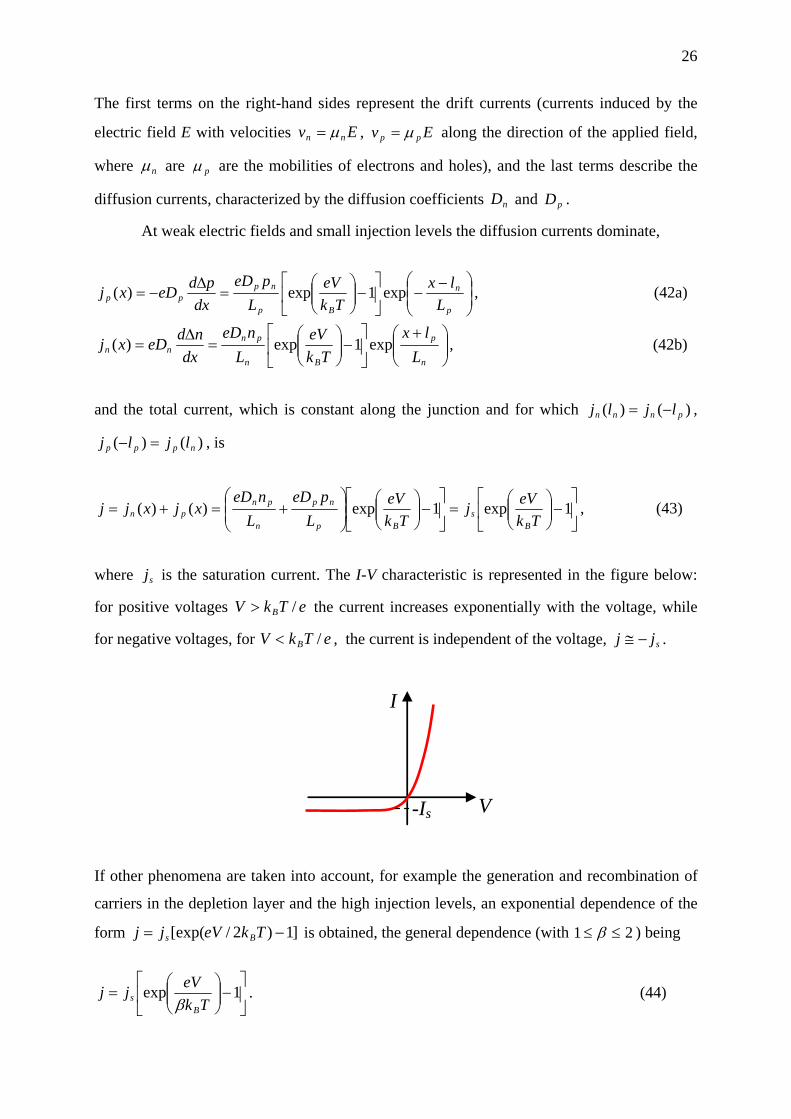
The I-V characteristics of a p-n junction
In the presence of an exterior voltage, the system of electrons is no longer in equilibrium, and
we must define Fermi quasi-levels for electrons in the p region, , as well as for those in
the n region, , since the concept of Fermi level makes sense only when the system of
electrons is at equilibrium. In the figure below we have represented the position of the Fermi
quasi-levels at inverse (left) and direct (right) polarizations.
FPE
FnE
EFn Ec
Ev
EFp eV
EFn Ec
Ev
EFp eV
n n
p
p
When an exterior voltage V is applied, minority carriers with concentrations and are
injected in the p and n regions, respectively, so that the carrier concentrations at the sides of
the depletion layer are
nΔ pΔ
)()/exp()( nnBnn lppTkeVplp Δ+== , )()/exp()( ppBpp lnnTkeVnln −Δ+==− . (39)
If and 0)( =−<<Δ plxn 0)( =>>Δ nlxp , the concentrations of injected carriers determined
by the diffusion equation are
⎟⎟⎠
⎞⎜⎜⎝
⎛ −−⎥
⎦
⎤⎢⎣
⎡−⎟⎟
⎠
⎞⎜⎜⎝
⎛=Δ
p
n
Bn L
lxTk
eVpxp exp1exp)( , ⎟⎟⎠
⎞⎜⎜⎝
⎛ +⎥⎦
⎤⎢⎣
⎡−⎟⎟
⎠
⎞⎜⎜⎝
⎛=Δ
n
p
Bp L
lxTk
eVnxn exp1exp)( , (40)
where , are the diffusion lengths in the two regions. For a steep junction and a narrow
depletion layer compared to the diffusion lengths,
nL pL
pn LLl ,<< , so that the recombination in
the layer can be neglected, the minority carrier currents in the p and n regions are,
respectively,
dxpdeDEppej pnpp
Δ−Δ+= )(μ ,
dxndeDEnnej npnn
Δ+Δ+= )(μ . (41)
26
The first terms on the right-hand sides represent the drift currents (currents induced by the
electric field E with velocities Ev nn μ= , Ev pp μ= along the direction of the applied field,
where nμ are pμ are the mobilities of electrons and holes), and the last terms describe the
diffusion currents, characterized by the diffusion coefficients and . nD pD
At weak electric fields and small injection levels the diffusion currents dominate,
⎟⎟⎠
⎞⎜⎜⎝
⎛ −−⎥
⎦
⎤⎢⎣
⎡−⎟⎟
⎠
⎞⎜⎜⎝
⎛=
Δ−=
p
n
Bp
nppp L
lxTk
eVL
peDdx
pdeDxj exp1exp)( , (42a)
⎟⎟⎠
⎞⎜⎜⎝
⎛ +⎥⎦
⎤⎢⎣
⎡−⎟⎟
⎠
⎞⎜⎜⎝
⎛=
Δ=
n
p
Bn
pnnn L
lxTk
eVL
neDdx
ndeDxj exp1exp)( , (42b)
and the total current, which is constant along the junction and for which )()( pnnn ljlj −= ,
, is )()( nppp ljlj =−
⎥⎦
⎤⎢⎣
⎡−⎟⎟
⎠
⎞⎜⎜⎝
⎛=⎥
⎦
⎤⎢⎣
⎡−⎟⎟
⎠
⎞⎜⎜⎝
⎛⎟⎟⎠
⎞⎜⎜⎝
⎛+=+= 1exp1exp)()(
TkeVj
TkeV
LpeD
LneD
xjxjjB
sBp
np
n
pnpn , (43)
where is the saturation current. The I-V characteristic is represented in the figure below:
for positive voltages the current increases exponentially with the voltage, while
for negative voltages, for , the current is independent of the voltage, .
sj
eTkV B />
eTkV B /< sjj −≅
I
V -Is
If other phenomena are taken into account, for example the generation and recombination of
carriers in the depletion layer and the high injection levels, an exponential dependence of the
form is obtained, the general dependence (with ]1)2/[exp( −= TkeVjj Bs 21 ≤≤ β ) being
⎥⎦
⎤⎢⎣
⎡−⎟⎟
⎠
⎞⎜⎜⎝
⎛= 1exp
TkeVjj
Bs β
. (44)

27
Light absorption The absorption of light in a material is characterized by the absorption coefficient α, which
represents the fraction of electromagnetic radiation absorbed per unit length in the material.
This can be expressed as
IdxdI α=− (45)
where I is the intensity of flux of light that propagates along the x direction and is normally
incident on the layer with width dx in the material, the – sign indicating that the intensity I
decreases as x increases. By integrating the equation above we obtain optical absorption law
)exp()1()( 0 xIRxI α−−= (46)
where is the intensity of light flux incident on the surface, and 0I 1<R is the reflection
coefficient of light. α represents the penetration depth of electromagnetic radiation at which
the flux intensity decreases e = 2.718 times. The average intensity of radiation that penetrates
a distance d inside the material is obtained by integrating the formula above, with the result
)]exp(1][/)1[()exp(]/)1[()( 00
0 ddIRdxxdIRdId
m ααα −−−=−−= ∫ (47)
I
x
(1-R)I0
dx
dI
I0
d
Im
This law is valid only for monochromatic light, because the absorption coefficient depends on
the light wavelength λ. The dependence of α on λ is characteristic for each material and is
determined by the physical processes that take place inside it.
Irrespective of the nature of physical processes, if the incident electromagnetic
radiation is considered to consist of photons with frequency ω, energy ωh=E and
wavevector k, the photon-illuminated material interaction occurs with the conservation of
both energy and momentum, which impose that

28
ωh=− if EE , (48)
kkk =− if , (49)
where and are the energy and momentum in the illuminated material in the final
(subscript f) and initial (subscript i) states.
ifE , if ,k
The nature of the interaction between photons and the illuminated material depends on
the photon energy. In semiconductors, the dominant absorption mechanism is the band-to-
band or fundamental absorption, in which an electron is promoted from the valence to the
conduction band as a result of photon absorption. In this case |||| if kkk −<< and the
electron momentum is conserved, the transition from the valence to the conduction band
being “vertical” in the k space (see the figure below).
E Ec
Eg
k
Ev
foton
Ei
Ef
α
Eg hω
If both conduction and valence bands are isotropic, parabolic and have extrema at , the
band-to-band absorption is direct, and the electron energy around the extrema of the two
bands can be written as , . Energy conservation
implies in this case the equality , where is the
reduced mass, defined through
0=k
ngf mkEE 2/22h+= pi mkE 2/22h−=
ωω hhh −+==−− rgif mkEEE 2/0 22rm
pnr mmm /1/1/1 += .
GaAs, GaSb, InP, InAs, CdS are examples of semiconductors with direct energy
bands. From (45) it follows that the absorption coefficient can be expressed as
,/)/)(/(/)/( IdtdIcnIdxdI refr−=−=α (50)

29
where is the refractive index of the semiconductor, c is the light velocity in vacuum, refrn
ωhNI = , with N the photon number in the incident radiation, and )/(/ dtdPdtdI totωh= is
the absorbed energy per unit time, with hω the photon energy and the transition
probability per unit time. A quantum calculation of the transition probability per unit time
leads to the following expression of the direct band-to-band absorption coefficient:
dtdPtot /
ωω
ααh
h gE−= 0 , (51)
with 0α an energy-independent term. The dependence of the absorption coefficient on the
frequency of incident photons is represented in the figure above. Note that the absorption has
a threshold at gp E=ωh , typical α values being of the order of 104–105 cm–1.
For impurified semiconductors with shallow energy levels and low concentrations of
the impurities, the discrete donor and acceptor levels, and , respectively, and the
possible transitions between these levels and between the impurity levels and the valence and
conduction bands are illustrated in the figure below, left.
dE aE
In this case the transition of charge carriers from the impurity levels on states in the
conduction or valence bands takes place as a result of absorption of one photon with energy
less than , so that the absorption spectrum has a lower threshold than for the fundamental
absorption mechanism. If, for example, there are only acceptor levels in the semiconductor,
the absorption spectrum overimposed on the fundamental absorption is represented in the
figure below, right. The absorption on impurities has a smaller intensity (the density of states
and hence the number of carriers on the acceptor level is much smaller than the carrier
number in the valence or conduction bands) and is shifted toward lower energies in
comparison to the fundamental absorption.
gE
Ec
Ed
Ea
Ev
α
Eg - EaEg
hω
30
The absorption on impurities can be observed for moderate concentrations of
impurities in doped semiconductors and for low impurity concentrations in compensated
semiconductors. For shallow impurity levels this absorption mechanism is observed in far
infrared (λ < 25 μm) and at low temperatures, in order to avoid the ionization of impurities.
The absorption coefficient α is proportional to the impurity concentration.
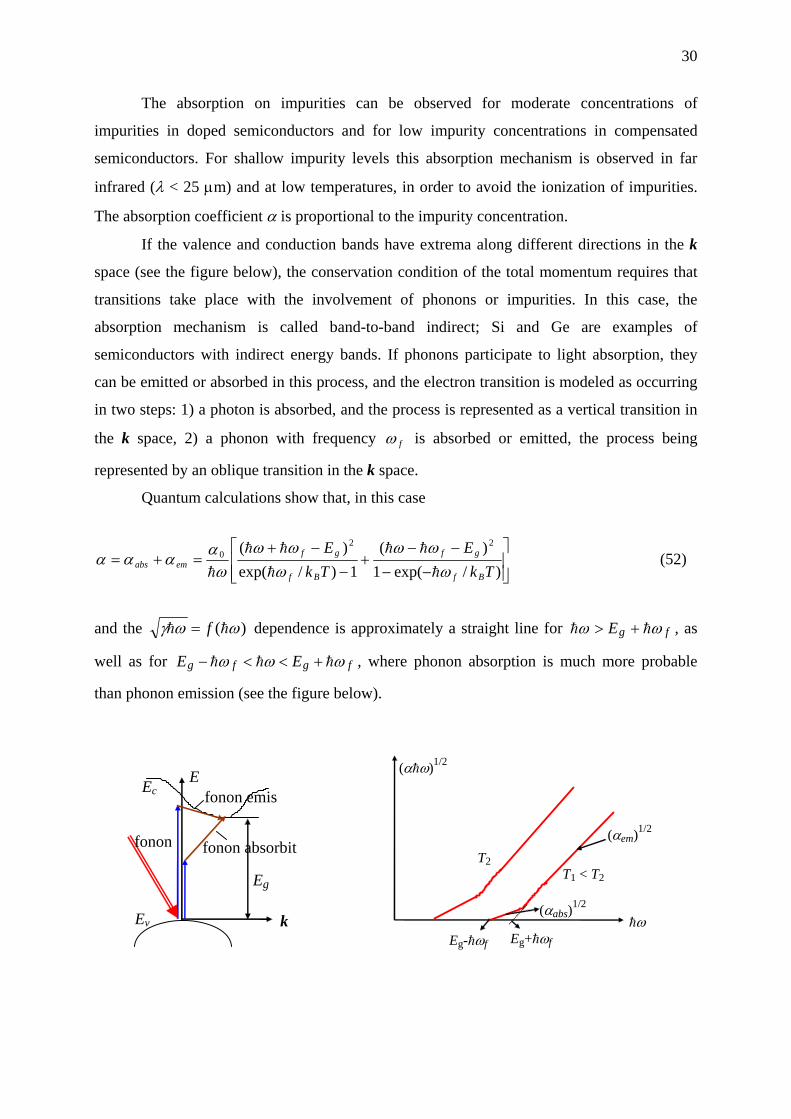
If the valence and conduction bands have extrema along different directions in the k
space (see the figure below), the conservation condition of the total momentum requires that
transitions take place with the involvement of phonons or impurities. In this case, the
absorption mechanism is called band-to-band indirect; Si and Ge are examples of
semiconductors with indirect energy bands. If phonons participate to light absorption, they
can be emitted or absorbed in this process, and the electron transition is modeled as occurring
in two steps: 1) a photon is absorbed, and the process is represented as a vertical transition in
the k space, 2) a phonon with frequency fω is absorbed or emitted, the process being
represented by an oblique transition in the k space.
Quantum calculations show that, in this case
⎥⎥⎦
⎤
⎢⎢⎣
⎡
−−−−
+−
−+=+=
)/exp(1)(
1)/exp()( 22
0
TkE
TkE
Bf
gf
Bf
gfemabs ω
ωωω
ωωω
ααααh
hh
h
hh
h (52)
and the )( ωωγ hh f= dependence is approximately a straight line for fgE ωω hh +> , as
well as for fgfg EE ωωω hhh +<<− , where phonon absorption is much more probable
than phonon emission (see the figure below).
E
fonon emis
fonon absorbit
k
Eg
Ev
Ec
fonon
T2 T1 < T2
hω
(αem)1/2
(αhω)1/2
(αabs)1/2
Eg-hωf Eg+hωf
31
Because there are several types of phonons in the crystal and more than one phonon
can be involved in the process, the absorption characteristics can have several discontinuities
that appear when the threshold at which new phonons can participate at the transition is
reached. For h hω ω> −Eg f the term in (52) related to phonon absorption dominates, while
for h hω ω> +Eg f phonon emission prevails. The absorption coefficient is smaller than at
direct transitions: ≅α 10–20 cm–1, and its temperature dependence is much more significant.
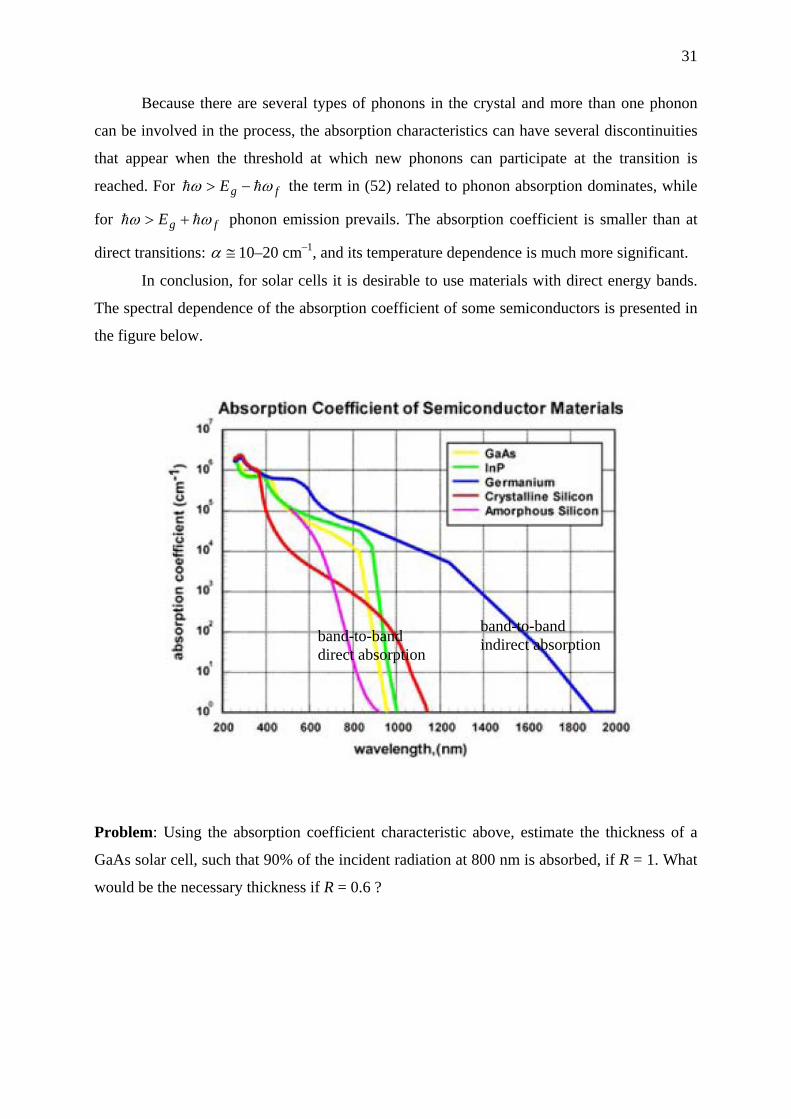
In conclusion, for solar cells it is desirable to use materials with direct energy bands.
The spectral dependence of the absorption coefficient of some semiconductors is presented in
the figure below.
band-to-band indirect absorption band-to-band
direct absorption
Problem: Using the absorption coefficient characteristic above, estimate the thickness of a
GaAs solar cell, such that 90% of the incident radiation at 800 nm is absorbed, if R = 1. What
would be the necessary thickness if R = 0.6 ?
32
The photoelectric effect
At the absorption of a photon with energy higher than or equal to the bandgap of a
semiconductor material, a bond between a pair of electrons or between an electron and a
positively charged nucleus is broken, so that a pair of electric charges consisting of a negative
electron and a positive hole is generated. These charges attract each other and recombine
unless they are spatially separated. A method for electron-hole separation is the application of
an electric field, due to which the electrons and holes are drifted in different directions so that
an electricity flux/a photocurrent appears. This is the working principle of solar cells. The
electric field can be, for example, the built-in field in a p-n junction.
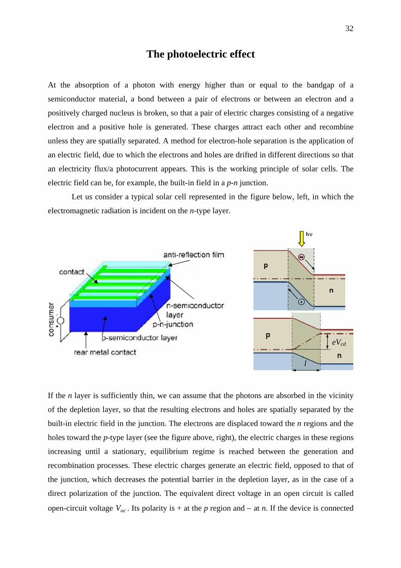
Let us consider a typical solar cell represented in the figure below, left, in which the
electromagnetic radiation is incident on the n-type layer.
eVcd
l
If the n layer is sufficiently thin, we can assume that the photons are absorbed in the vicinity
of the depletion layer, so that the resulting electrons and holes are spatially separated by the
built-in electric field in the junction. The electrons are displaced toward the n regions and the
holes toward the p-type layer (see the figure above, right), the electric charges in these regions
increasing until a stationary, equilibrium regime is reached between the generation and
recombination processes. These electric charges generate an electric field, opposed to that of
the junction, which decreases the potential barrier in the depletion layer, as in the case of a
direct polarization of the junction. The equivalent direct voltage in an open circuit is called
open-circuit voltage . Its polarity is + at the p region and − at n. If the device is connected ocV

33
in series with a load , a photocurrent flows in the exterior circuit in an opposite direction
than in the case when the non-illuminated (dark) junction would have been polarized to an
external source at the same (direct) voltage. In consequence, the photocurrent has the same
direction as the inverse (saturation) current of the non-illuminated junction, the solar cell
generating the current (see the figure below). The total current is then
sR
LI
⎥⎦
⎤⎢⎣
⎡−⎟⎟
⎠
⎞⎜⎜⎝
⎛+−= 1exp
TkeVIII
BsL β
. (53)
I
V
-IL
dark
illumination
-Is
V=-RsI
V Voc
P
I
Isc
Vm
Im
A closer look at the characteristic of the photoelement (see the figure above,
right) for V > 0, I < 0, allows us to define two important parameters of the solar cell: the open-
circuit voltage,
VI −
)/1ln()/( sLBoc IIeTkV += β , which is the voltage that corresponds to I = 0,
and the short-circuit current, Lsc II −= , which corresponds to V = 0. In applications, it is
common to consider the dependence with the opposite current (with I > 0). The open-
circuit voltage can not be smaller than the energy bandgap of the semiconductor (divided by
the electron charge), whereas the photocurrent is determined by the intensity of the solar
radiation (by the number of photons with energy higher than the bandgap).
VI −
Moreover, the performance of a solar cell is determined by the (output) power IVP =
on the load. The working point (i.e., the voltage and current) are found from the intersection
of the characteristics and the straight line defined by VI − IRV s−= , the power being given
by the are of the rectangle formed from the voltage and current values in the working point.
The power dependence on voltage (the blue line in the figure above, right) has a maximum

34
defined by (see the gray area) for which 0/ =dVdP mII = , mVV = . The maximum power
is generated on the load mmm VIP = mmsm IVR /−= . To optimize the power a compromise
between a high current and a high voltage is generally necessary.
A solar cell is characterized by the filling factor (or filling ratio)
ocscmm VIVIFF /= (54)
and the conversion efficiency
=η output power/input power (55) radm PP /=
where is the power of the incident solar radiation. Both parameters have values less than
unity. The typical conversion efficiency has values of 12−20% for standard solar cells, while
a typical filling factor is 75%.
radP
In addition, for a better comparison of the materials from which the solar cell is
fabricated, one can define the external quantum efficiency as the number of collected
electrons per incident photon,
=extη collected electrons/incident photons. (56)
This parameter is within the 60−90% range, depending on the reflectivity, wavelength and
illumination conditions. Another useful parameter is the internal quantum efficiency, defined
as the number of collected electrons per absorbed photon,
iη = collected electrons/absorbed photons (57)
which has typical values of 80−95%, depending on the wavelength.
Efficient solar cells have high conversion efficiency, hence high external quantum
efficiency, and can transform in electric energy photons in a wide spectral range. In the next
parts of the course we will analyze the performances of solar cells from different generations
and will discuss the solutions for improving their efficiency.


![Bases Bases Bases Bases Bases Bases Bases Bases Bases ......Hair loss or alopecia is a problem in modern society, which is usually related to hair loss on the scalp [1]. The most common](https://img.pdfslide.us/doc/110x75/5f692ed64ffcd531a566bfdf/bases-bases-bases-bases-bases-bases-bases-bases-bases-hair-loss-or-alopecia.jpg)