Embed Size (px)
Citation preview
PES analysis of donor/acceptor and p-doped-donor/acceptor organic heterojunctions: CuPc/BPE-PTCDI and (CuPc+WO3)/BPE-PTCDI
Thomas Mayer, Corinna Hein, Eric Mankel, and Wolfram JaegermannDarmstadt University of Technology, Institute of Materials Science
Petersenstr. 23, D-64287 Darmstadt, Surface Science Division
Due to low dielectric constants and strong intra and extra-molecular relaxation in organic semiconductors optically generated electron hole pairs form strongly bound excitons of 0.5 to 1eV binding energy. In organic solar cells hetero-junctions of electron donor and acceptor materials are used for dissociation of the excitons and charge separation (Fig.1). After injection of the electron from the donor to the acceptor electron hole pairs may be bound across the hetero-junction forming so called geminate pairs still likely to undergo recombination. The electronic structure of such organic hetero-interfaces concerning band/orbital line up and potential gradients is of basic importance for the cell efficiency.
Fig.1: Exciton dissociation and charge separation at the donor acceptor hetero-junction interface in organic solar cells.
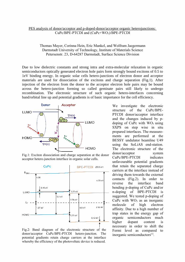
Fig.2: Band diagram of the electronic structure of the donor/acceptor CuPc/BPE-PTCDI hetero-junction. The potential gradients retain charge carriers at the interface whereby the efficiency of the photovoltaic device is reduced.
We investigate the electronic structure of the CuPc/BPE-PTCDI donor/acceptor interface and the changes induced by p-doping of CuPc with WO3 using SXPS on step wise in situ prepared interfaces. The measurements are performed at the BESSY undulator beamline U49 using the SoLiAS end-station. The electronic structure of the donor/acceptor system CuPc/BPE-PTCDI indicates unfavourable potential gradients that retain the separated charge carriers at the interface instead of driving them towards the external contacts (Fig.2). In order to reverse the interface band bending p-doping of CuPc and/or n-doping of BPE-PTCDI is suggested. We tested p-doping of CuPc with WO3 as an inorganic molecule of high electron affinity. Due to a high number of trap states in the energy gap of organic semiconductors much higher dopant content is necessary in order to shift the Fermi level as compared to inorganic semiconductors[1].
.
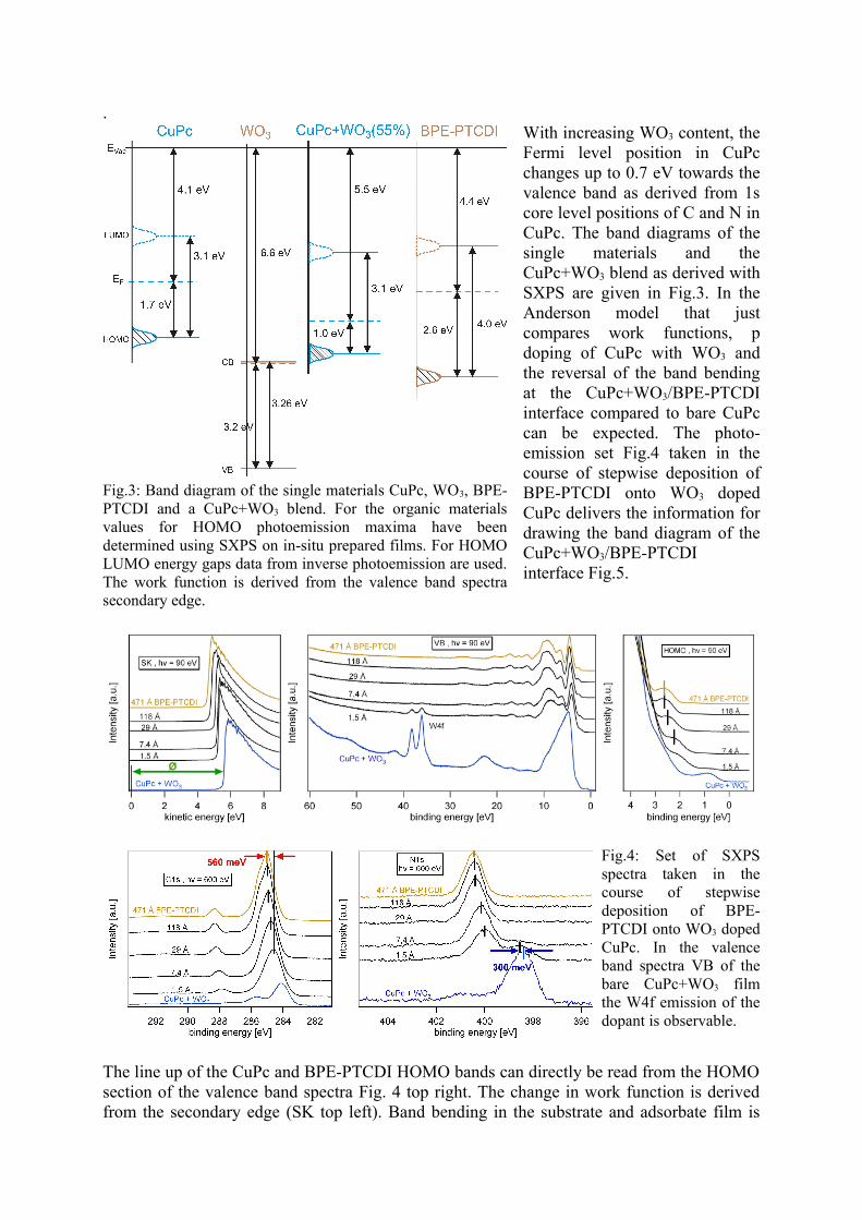
Fig.3: Band diagram of the single materials CuPc, WO3, BPE-PTCDI and a CuPc+WO3 blend. For the organic materials values for HOMO photoemission maxima have been determined using SXPS on in-situ prepared films. For HOMO LUMO energy gaps data from inverse photoemission are used. The work function is derived from the valence band spectra secondary edge.
With increasing WO3 content, the Fermi level position in CuPc changes up to 0.7 eV towards the valence band as derived from 1s core level positions of C and N in CuPc. The band diagrams of the single materials and the CuPc+WO3 blend as derived with SXPS are given in Fig.3. In the Anderson model that just compares work functions, p doping of CuPc with WO3 and the reversal of the band bending at the CuPc+WO3/BPE-PTCDI interface compared to bare CuPc can be expected. The photoemission set Fig.4 taken in the course of stepwise deposition of BPE-PTCDI onto WO3 doped CuPc delivers the information for drawing the band diagram of the CuPc+WO3/BPE-PTCDI interface Fig.5.
Fig.4: Set of SXPS spectra taken in the course of stepwise deposition of BPE-PTCDI onto WO3 doped CuPc. In the valence band spectra VB of the bare CuPc+WO3 film the W4f emission of the dopant is observable.
The line up of the CuPc and BPE-PTCDI HOMO bands can directly be read from the HOMO section of the valence band spectra Fig. 4 top right. The change in work function is derived from the secondary edge (SK top left). Band bending in the substrate and adsorbate film is
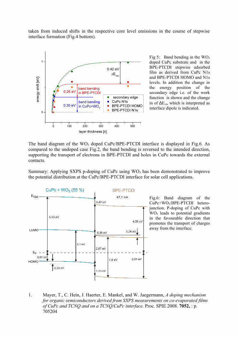
taken from induced shifts in the respective core level emissions in the course of stepwise interface formation (Fig.4 bottom).
Fig 5: Band bending in the WO3
doped CuPc substrate and in the BPE-PTCDI stepwise adsorbed film as derived from CuPc N1s and BPE-PTCDI HOMO and N1s levels. In addition the change in the energy position of the secondary edge i.e. of the work function is shown and the change in of ∆Evac which is interpreted as interface dipole is indicated.
The band diagram of the WO3 doped CuPc/BPE-PTCDI interface is displayed in Fig.6. As compared to the undoped case Fig.2, the band bending is reversed to the intended direction, supporting the transport of electrons in BPE-PTCDI and holes in CuPc towards the external contacts.
Summary: Applying SXPS p-doping of CuPc using WO3 has been demonstrated to improve the potential distribution at the CuPc/BPE-PTCDI interface for solar cell applications.
Fig.6: Band diagram of the CuPc+WO3/BPE-PTCDI hetero-junction. P-doping of CuPc with WO3 leads to potential gradients in the favourable direction that promotes the transport of charges away from the interface.
1. Mayer, T., C. Hein, J. Haerter, E. Mankel, and W. Jaegermann, A doping mechanism for organic semiconductors derived from SXPS measurements on co-evaporated films of CuPc and TCNQ and on a TCNQ/CuPc interface. Proc. SPIE 2008. 7052, : p. 705204