Embed Size (px)
Citation preview

HAL Id: hal-00875712https://hal.archives-ouvertes.fr/hal-00875712
Submitted on 22 Oct 2013
HAL is a multi-disciplinary open accessarchive for the deposit and dissemination of sci-entific research documents, whether they are pub-lished or not. The documents may come fromteaching and research institutions in France orabroad, or from public or private research centers.
L’archive ouverte pluridisciplinaire HAL, estdestinée au dépôt et à la diffusion de documentsscientifiques de niveau recherche, publiés ou non,émanant des établissements d’enseignement et derecherche français ou étrangers, des laboratoirespublics ou privés.
Correlation between structural and optical properties ofWO3 thin films sputter deposited by glancing angle
depositionCédric Charles, Nicolas Martin, Michel Devel, Julien Ollitrault, Alain Billard
To cite this version:Cédric Charles, Nicolas Martin, Michel Devel, Julien Ollitrault, Alain Billard. Correlation betweenstructural and optical properties of WO3 thin films sputter deposited by glancing angle deposition.Thin Solid Films, Elsevier, 2013, 534, pp.275 - 281. <10.1016/j.tsf.2013.03.004>. <hal-00875712>
1
Correlation between structural and optical properties of WO3 thin films sputter 1
deposited by glancing angle deposition 2
3
Cédric CHARLES a, Nicolas MARTIN a, 1, Michel DEVEL a, Julien OLLITRAULT a, 4
Alain BILLARD b 5
6
a Institut FEMTO-ST, UMR 6174 CNRS, Université de Franche-Comté, ENSMM, UTBM 7
32, Avenue de l’observatoire, 25044 BESANCON Cedex, France 8
9
b LERMPS, UTBM, Site de Montbéliard, 90010 BELFORT Cedex, France 10
1 Author to whom correspondence should be addressed: Tel.: +33 (0)3 81 85 39 69; Fax: +33 (0)3 81 85 39 98; Email:
nicolas.martin@femtoͲst.fr
2
Abstract 11
Tungsten oxide WO3 thin films are prepared by dc reactive sputtering. The GLancing Angle 12
Deposition method (GLAD) is implemented to produce inclined columnar structures. The incident 13
angle α between the particle flux and the normal to the substrate is systematically changed from 0 14
to 80°. For incident angles higher than 50°, a typical inclined columnar architecture is clearly 15
produced with column angles β well correlated with the incident angle α according to conventional 16
relationships determined from geometrical models. For each film, the refractive index and 17
extinction coefficient are calculated from optical transmittance spectra of the films measured in the 18
visible region. The refractive index at 589 nm drops from n589 = 2.18 down to 1.90 as α rises from 0 19
to 80°, whereas the extinction coefficient reaches k589 = 4.27×10⁻³ for an incident angle α = 80°, 20
which indicates that the films produced at a grazing incident angle become more absorbent. Such 21
changes of the optical behaviours are correlated with changes of the microstructure, especially a 22
porous architecture, which is favoured for incident angles higher than 50°. Optical band gap Eg, 23
Urbach energy Eu and birefringence ∆n617, determined from optical transmittance measurements, 24
are also influenced by the orientation of the columns and their trend are discussed taking into 25
account the disorder produced by the inclined particle flux. 26
27
Keywords 28
WO3 films, GLAD, inclined columns, refractive index, porosity, optical band gap, Urbach energy, 29
birefringence. 30
3
1. Introduction 31
Transition metal oxides represent a very attracting class of materials because of the wide range of 32
physical and chemical properties that they exhibit. Among these oxide compounds, tungsten oxide 33
thin films have been extensively investigated due to their important applications as active layers for 34
electrochromic window devices [1-4], sensors for toxic gases [5-8], optical coatings with high 35
refractive index [9, 10] or transparent and low resistive oxide materials [11, 12]. It is well known 36
that many chemical and physical characteristics of metal oxide thin films are strongly connected to 37
their chemical composition, especially the oxygen-to-metallic concentrations ratio, which can be 38
tuned in order to get a metallic, semi-conducting or insulating behaviour according to the metalloid 39
content in the film [13-16]. However, playing with the chemical composition is not the only 40
approach to tune the properties of metal oxide thin films. The structure at the sub-micrometric scale 41
can also influence the film performances for many applications [17]. So, the design and the growth 42
control of nanostructures in thin layers appear as important issues, e.g. in order to control the optical 43
properties by playing on structural features. To this aim, various strategies have been proposed for 44
the structuration of thin films [18]. 45
In the last decade, the interest of nanostructuration by evaporation and/or sputtering techniques was 46
particularly boosted by the GLancing Angle Deposition (GLAD) method [19]. This method is based 47
on the preparation of thin films on fixed or mobile substrate, with an oblique incidence of the 48
incoming particle flux. Indeed, when the atomic vapour flow comes up at a non normal incident 49
angle α, the nucleation sites intercept the flow of particles. This creates a shadowing effect and 50
there is a tilted grain growth of columnar shape leading to inclined columnar structures with an 51
angle β with respect to the normal of the substrate surface. Nature, crystallography, temperature and 52
surface conditions of the substrate, energy and interactions of the condensed particles with the 53
substrate, among other parameters, have a decisive role in the growth mode of the coating. As a 54
result, the GLAD technique can control the structure of thin films at the micro- and nanoscales. The 55
experimental setup has two degrees of freedom: a rotation axis at an angle α, which allows to vary 56
4
the incident angle of the particle flux, and a rotary axis at an angle φ (also called azimuth angle), 57
which modifies in an indirect way, the position of the particle source. The produced architectures 58
can be of type i) columnar and inclined; ii) chevron or zigzag by alternating periodically the 59
incident angle of particles from +α to -α maintaining constant φ angle (azimuthal angle around the 60
substrate) or with a 180° rotation of φ keeping constant α angle; iii) spiral or helical thanks to a 61
continuous rotation of φ at a constant incident angle α. This latter type adds to the potential of the 62
GLAD technique. Morever, changing wisely α and φ angles as well as speeds of rotation, more 63
original structures can be obtained such as porous columnar structures with variable diameters [20] 64
or helical columns with squared sections [21]. In the end, the GLAD technique exploits the effects 65
of shadowing created by a tilted substrate relative to normal incidence and a change of the direction 66
of the particle flux through a rotation of the same substrate during the deposition. The two 67
combined can generate different forms of columns and varied architectures. For example, Robbie et 68
al. [22, 23] or Van Popta et al. [24] have deposited by evaporation some structured films with 69
columnar architectures showing sinusoidal, helical and more complex forms. This variety allows 70
envisaging applications in many fields such as biomedical system [25], photonic devices [26], 71
microsensors [27], etc. Moreover thin films deposited by GLAD have high porosity and anisotropic 72
behaviours, which can be used as rugate filters [28], wavelength-selective polarizer [29], or 73
antireflection coating [30]. 74
The purpose of this article is to study the structural and optical properties of the sputter deposited 75
tungsten oxide WO3 nanostructured thin films grown using various incident angles Į of the particle 76
flux from 0 to 80°. We systematically investigate how the structure and optical properties 77
(refractive index, extinction and absorption coefficients, optical band gap, birefringence) of such 78
oriented thin films can be tuned by changing the incident angle of the sputtered particles. The 79
evolution of the porous structure connected to the columnar orientation is especially analyzed in 80
order to discuss and understand some relationships between the architecture of the films and their 81
resulting optical behaviours. 82

5
83
2. Experimental details 84
WO3 films were sputter deposited by DC reactive magnetron sputtering using a home made system 85
[31, 32]. A tungsten target (5 cm diameter with purity 99.9 at. %) was powered at a constant current 86
density J = 25.5 A.m-2, with an argon partial pressure PAr = 0.1 Pa and an oxygen partial pressure 87
PO2 = 0.08 Pa. Substrates (grounded and kept at room temperature) were glass plates and (100) 88
silicon wafers. The distance between the target and the substrate was fixed at 60 mm. The growth of 89
the films was stopped at a thickness close to 1 µm thanks to the calibration of the deposition rate. A 90
systematic change of the incident angle from Į = 0 to 80° with a 10° increment was performed to 91
tune the inclined columnar structure. Films deposited on glass substrates were characterized thanks 92
to optical transmittance spectra measured with a Lambda 900 Perkin Elmer spectrophotometer in 93
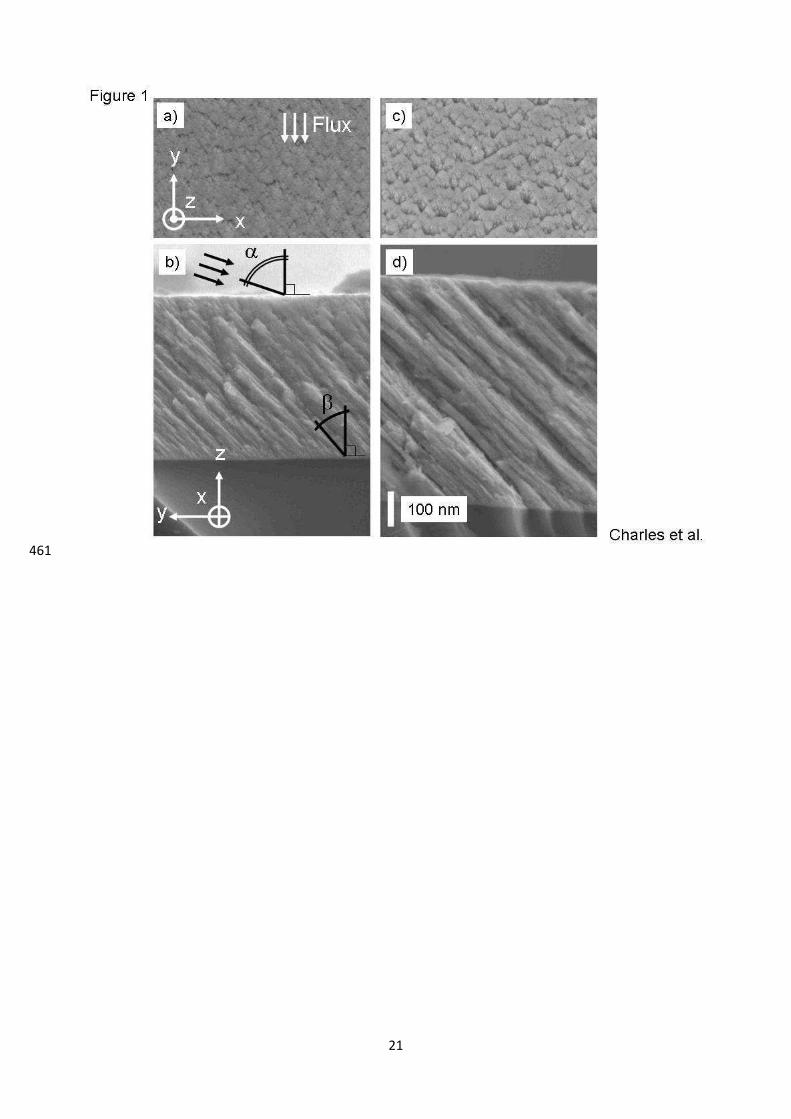
the visible range from 1.55 to 3.10 eV (i.e. wavelength in-between 800 to 400 nm). Refractive 94
index, extinction coefficient and absorption coefficient were determined from interference fringes 95
obtained with experimental optical transmittance spectra using Swanepoel’s method [32]. Films 96
prepared on (100) silicon wafers were cross-sectioned and observed by field effect scanning 97
electron microscopy (SEM) using a JEOL 6400 F. WO3 structures were also characterized by X-ray 98
diffraction (XRD). Measurements were carried out using a Bruker D8 focus diffractometer with a 99
cobalt X-ray tube (Co ȜKɲ = 1.78897 Å) in a θ/2θ configuration. 100
101
3. Results and discussion 102
3.1 Structural characterization 103
Tungsten oxide thin films prepared with an incident angle α lower than 50° do not exhibit a clear 104
inclined columnar structure. A densely packed feature is rather observed with a smooth surface 105
topography. However, a further increase of the incident angle (α higher than 50°) leads to a rougher 106
film/air interface and a more defined columnar growth. Observations by SEM of surfaces and cross-107
sections of WO3 thin films sputter deposited with an incident angle α of 70 and 80° are shown in 108

6
figure 1. It is worth of noting that the top of the columns has a rather sharp appearance (Fig. 1a), 109
which is even more emphasized for α = 80° (surface state becomes irregular and more voided as 110
illustrated in figure 1c). Such increase of the surface roughness versus incident angle of the 111
sputtered particles is in agreement with previous investigations focused on metal oxide coatings 112
produced by GLAD [33, 34]. It is mainly attributed to the shadowing effect at the atomic scale, 113
which prevails over the surface diffusion of adatoms as the incident angle rises. The structural 114
anisotropy (formation of growth islands connected to each other by chains perpendicular to the 115
plane of incidence) previously claimed by Tait et al. [35], is slightly marked for sputtered tungsten 116
oxide films. The top of the columns appears more or less connected to each other according to the x 117
direction and perpendicular to the particle flux (Fig. 1a and 1c). 118
Inspection of the cross-sectional view ensures that the GLAD WO3 films are composed of slanted 119
columns and inter-columnar voids (Fig. 1b and 1d). The columns are inclined towards the direction 120
of the incoming vapour flux. The column angle ȕ, defined as the angle between the substrate surface 121
normal and the long axis of the slanted columns, is measured from the cross-section SEM images. 122
For incident angle α lower than 50°, the column angle ȕ can not be accurately determined since no 123
clear columnar growth has been produced but a densely packed structure. For higher angles of 124
incidence (α > 50°), SEM images exhibit morphologies composed by columns and inter-columnar 125
gaps. The columns become increasingly separated and can easily be distinguished at an incident 126
angle α of 70° and even more at 80°. The resulting column angles β are 50 and 54° for incident 127
angles α of 70 and 80°, respectively. Such column angles deviate from the empirical tangent rule 128
[36], which predicts 53 and 70°, respectively. This rule provides a first order approximation of the 129
expected β angles. Since the growth can be disturbed by many parameters (temperature, particle 130
energy, pressure), the tangent rule fails to well describe experimental column angles, especially for 131
grazing incident angles. This is indeed relevant for thin films deposited by the sputtering process, 132
where column angles are often lower than those calculated with various ballistic rules [37, 38]. 133
However, our produced WO3 column angles are in good agreement with relationships proposed by 134

7
Tait et al. [39]. The sputtering pressure required to maintain the glow discharge restricts the mean 135
free path of the sputtered particles and thus, reduces the shadowing effect. As a result, the 136
theoretical column inclinations predicted by the simple tangent rule is systematically overestimated. 137
Since tungsten oxide thin films have been deposited at room temperature (substrate temperature is 138
lower than 0.3 times the melting point of WO3 compound), one could expect a poorly crystallized 139
material. However, XRD analyses exhibit diffracted signals (Fig. 2). Peaks corresponding to the 140
WO3 monoclinic structure are clearly identified for incident angles included between α = 0 and 80°. 141
For normal incidence (α = 0°), as-deposited films are weakly crystallized since the major diffracted 142
peaks exhibit low intensity and the average crystallite size calculated from the Scherrer equation is 143
smaller than 15 nm. An increase of the incident angle α up to 40° leads to more intense peaks for all 144
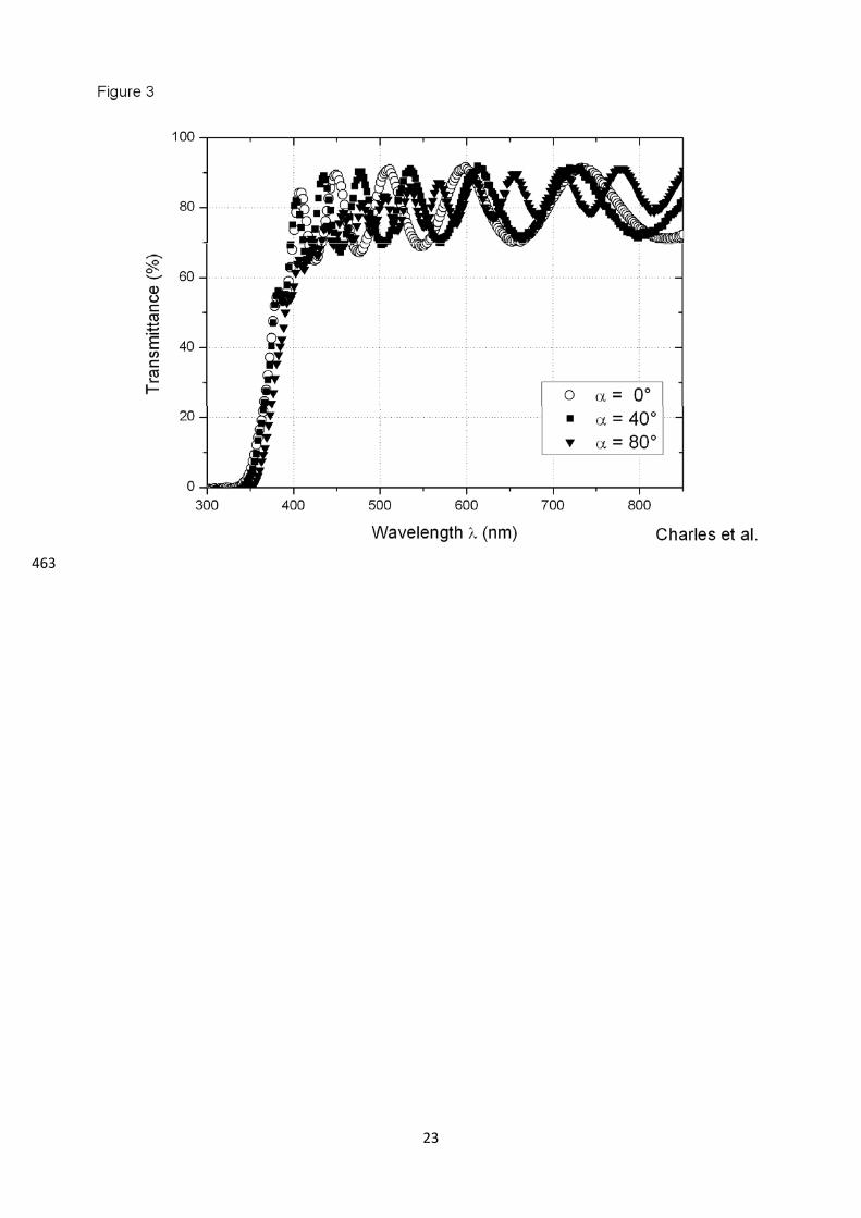
crystallographic planes, without any preferential orientation. In addition, the crystallite size reaches 145
30 nm for α = 40° and the diffracted patterns (peaks position, intensity or full-width-at-half-146
maximum) do not evolve as the incident angle α increases up to 80°. This improved crystallinity as 147
a function of the incident angle has also been observed for other ceramic thin films produced by 148
GLAD [40, 41]. In addition, a reverse effect has been observed by others for some materials [42], 149
showing a reduction of the long range order up to an amorphous structure as the incident angle α 150
rises. As a result, the dependence of crystallinity on the deposition angle has to be considered on a 151
case by case basis and still remains an open question. Nevertheless, it can be correlated with the 152
surface diffusion phenomenon of the sputtered particles. This phenomenon preferentially takes 153
place in the direction of the particle flux, particularly for grazing incident angles. During initial 154
growth and as the incident angle α increases, the formed islands start collecting more adatoms. 155
They will grow faster and tend to capture more incoming vapour flux, reinforcing the growth of 156
large crystallites at the expense of other grains that are consumed during the process. This possible 157
explanation of the long range crystalline order is in agreement with the increase of the crystallite 158
size reported from XRD measurements since grain size rises from 15 to 30 nm as the incident angle 159
α changes from 0 to 40°, and finally 80°. 160
8
161
3.2 Optical characterization 162
Optical transmittance spectra of tungsten oxide films deposited on glass substrates have been 163
measured in the visible region for various incident angles α of the particle flux (Fig. 3). As expected 164
for WO3 compound, typical interference fringes are observed. The films deposited by conventional 165
process (α = 0°) exhibit the highest amplitudes. For a given wavelength (e.g. 600 nm) the envelop 166
curve is below 70 % for the minimum of transmittance (Tmin), whereas it is higher than 91 % for the 167
maximum of transmittance (TMax). Amplitude of the fringes is slightly reduced up to an increasing 168
incident angle α = 40°. The amplitudes reduction becomes more significant for grazing incident 169
angles, especially for α = 80° since Tmin is close to 77 % and TMax is 88 % at 600 nm. For this high 170
incident angle of 80°, it is also worth of noting that fringes tend to disappear as the wavelength 171
comes closer to the absorption edge (i.e. between 400 and 500 nm), which can be attributed to the 172
enhancement of the light diffusion. This later is not solely due to structural modification in the film 173
(columns are more inclined), but it also comes from an increased surface roughness for incident 174
angles higher than 40°, as previously observed from SEM analyses (Fig. 1) and in agreement with 175
other theoretical and experimental investigations [43]. 176
From optical transmittance measurements of the WO3 films deposited on glass substrate, refractive 177
index n (Fig. 4) and extinction coefficient k (Fig. 5) have been calculated as a function of the 178
wavelength in the visible region using the Swanepoel’s method [44]. The refractive index and 179
extinction coefficient dispersion curves of WO3 films deposited at various incident angles are all 180
fitted by using the Cauchy dispersion equation in the range of wavelengths 400 to 800 nm. Both the 181
optical index and extinction coefficient follow the Cauchy dispersion evolution as a function of 182
wavelength for any incident angle of the particle flux. WO3 thin films prepared with a normal 183
incidence of the particle flux (α = 0°) exhibit the highest refractive index together with the lowest 184
extinction coefficient. For a reference wavelength of 589 nm, n589 = 2.17 (and k589 is below 1.42×10-185
3). This value is below that of the bulk WO3 material since nbulk = 2.50 for the same given 186

9
wavelength [45]. It shows that the films sputter deposited at normal incidence are quite compact but 187
nonetheless contain significant amounts of defects and voids. 188
A systematic change of the incident angle of the particle flux from 0 to 80° leads to a clear decrease 189
of the refractive index of tungsten oxide thin films from n589 = 2.17 down to 1.90, respectively. This 190
drop becomes very significant when the incident angle is higher than 40°. This effect has already 191
been observed for other metallic oxide thin films prepared by GLAD [46-48]. It is mainly ascribed 192
to the growth of a more porous structure versus incident angle. In evaporation or sputtering 193
processes, the deposited film’s planar density is determined by the shadow length and thus, can be 194
tuned by the incident angle α. Varying the amount of bulk material in the film is a way to change its 195
refractive index. 196
Similarly, extinction coefficient is nearly constant close to 1.50×10⁻³ at 589 nm up to an incident 197
angle of 60°. Hence, it remains close to values corresponding to typical dielectric and transparent 198
compounds. However, for an incident angle of 80° where k589 is higher than 4.27×10⁻³. Such 199
increase of the extinction coefficient correlates with the increase of the surface roughness 200
commonly measured for high incident angles. Indeed, the low values of k in the visible region is a 201
qualitative indication of the good surface smoothness of thin films [49]. Furthermore, the high k 202
value obtained for α = 80° suggests the presence of marked inhomogeneities in the films (defects, 203
disordering, oxygen vacancies, surface corrugation), especially a rougher film/air interface favoured 204
for high glancing angles of deposition. 205
The packing density p and, hence, the porosity π of the WO3 GLAD films (π = 1 – p) are significant 206
characteristics of sputter deposited materials. They can be calculated based on the effective media 207
approximation, and thus using the mixture rule proposed by Bruggemann [50]: 208
02 2
a eff b eff
a b
a eff b eff
ε ε ε εχ χε ε ε ε − −+ = + × + × (1) 209
Where a and b components are randomly distributed in space with volume fractions of χa and χb, 210
respectively (χa + χb = 1). The dielectric properties of the medium are described by an effective 211

10
permittivity εeff, and that of a and b components are εa and εb, respectively. For our films, we 212
considered that a component is the WO3 bulk material and b component is the vacuum. As a result, 213
εeff is the permittivity of the film. Assuming that the bulk tungsten trioxide compound has a 214
refractive index of nb = 2.50 at 589 nm [45] and from the refractive index of the film nf at 589 nm, 215
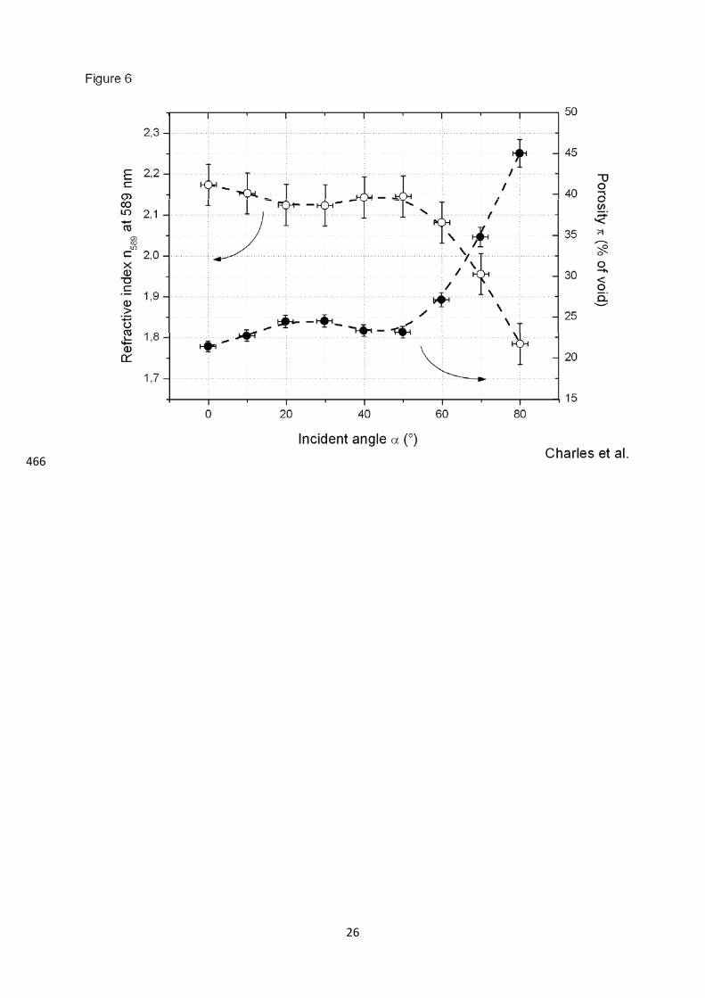
packing density and so, porosity have systematically been calculated and compared to the refractive 216
index as a function of the incident angle α (Fig. 6). Refractive index and porosity exhibit a reverse 217
evolution as the incident angle α rises. WO3 films deposited by conventional incidence (α = 0°) 218
show the highest refractive index with n589 = 2.18 and thus, the lowest porosity with π lower than 219
21 %. As expected, index is below that of the bulk material because of the total sputtering pressure 220
(0.18 Pa) used to deposit the films. Thermalisation effect of the sputtered particles and especially, 221
intrinsic low energy bombardment in sputtered thin films are both influenced by the sputtering 222
pressure. They can favour a structure with an open grain boundaries and large columns, leading to a 223
significant void fraction in the deposited film. As a result, density of WO3 deposited film is lower 224
than that of the bulk. 225
It is also worth of noting that refractive index and porosity are nearly constant up to an incident 226
angle of 50°. Index rapidly drops from n589 = 2.14 down to 1.78 when α changes from 50 to 80° 227
whereas the porous structure is enhanced and π reaches 45 % for α = 80°. It is mainly attributed to 228
the shadowing effect, which prevails on the surface diffusion of adatoms increasing the deposition 229
angle. These results well agree with previous investigations focused on oxide thin films [47, 48]. 230
Varying the amount of bulk material in the film provides a means of tuning its optical properties 231
according to a monotonic and continuous relationship between n and α. For highly oblique angles 232
(α > 80°), refractive index should approach unity and porosity should tend to 100 %. However, the 233
lowest index and thus the maximum porosity for WO3 coatings prepared in this study, obviously 234
depend on the film preparation conditions, but the measurements techniques (spectrometry in 235
transmission by Swanepoel’s method, ellipsometry) and environment (humidity) can also influence 236
the reachable index and porosity values. 237

11
Because of the peculiar architecture of the GLAD thin films, anisotropic behaviours like 238
birefringence can also be expected. Thus, transmittance spectra were measured with two x and y 239
orthogonal directions of incident linear polarized light (Tx and Ty in the x and y directions, 240
respectively and according to axes defined in Fig. 1). The in-plane birefringence is defined as the 241
difference between the two in-plane refractive indices ∆n = nx – ny, where nx and ny are determined 242
by the Swanepoel’s method from Tx and Ty, respectively. Figure 7 illustrates the influence of the 243
incident angle α on the birefringence ∆n calculated at 617 nm. This birefringence first increases 244
with the incident angle then reaches a maximum value of ∆n = 0.023 for α = 50°. The fact that there 245
is an optimised birefringence was also reported by other authors for ZrO2 [42], ZnS [48], Ta2O5 [51] 246
or TiO2 [52] films. Furthermore, the value of the maximum ∆n can be enhanced using a serial 247
bideposition technique as described by Hodginkson and Wu [51]. For tilted columnar films 248
prepared from standard oblique deposition, the highly porous structure obtained for the highest 249
incident angles does not improve the optical anisotropy. The optimized birefringence can not solely 250
be connected to the porosity, but rather to the biaxial columnar structure. This latter is especially 251
produced for incident angles close to 60°. From simulations and experiments performed by Tait et 252
al. [35], films produce a columnar structure with columns exhibiting an elliptical section versus the 253
incident angle. A structural anisotropy develops parallel to the substrate surface because of the 254
shadowing effect. This effect, mainly in the direction of the incident vapour flux, leads to the 255
formation of growth islands connected to each other by chains perpendicular to the plane of 256
incidence or to the direction of shadowing. The authors established that for an incident angle close 257
to 60°, the shadowing effect prevails on the surface diffusion. By further increasing the α angle, the 258
number of islands falls because of shadowing effect is even more marked. Consequently, the 259
average distance between islands increases. Then, they become disconnected from each other in all 260
directions, resulting in a loss of anisotropy. 261
12
The Swanepoel’s method can also be used to calculate the evolution of the absorption coefficient ξ 262
as a function of wavelength. Therefore, the optical band gap Eg of WO3 films can be determined 263
from the Tauc’s relationship according to the following equation [53]: 264
( )w
gh C h Eξ υ υ= − (2) 265
Where C is a constant and w is 1/2, 3/2, 2 or 3 for transitions being direct and allowed, direct and 266
forbidden, indirect and allowed, and indirect and forbidden, respectively. The values of optical band 267
gap energy Eg can be obtained by extrapolating the absorption coefficient to zero absorption in the 268
(ξhν)1/w against photon energy hν plot. According to Hjelm et al. [54], WO3 compound exhibits 269
indirect and allowed band gap transitions with w = 2. Thus, the Eg value was extracted from (ξhν)1/2 270
versus hν plot for WO3 films prepared with different incident angles (Fig. 8). Without inclining the 271
particle flux (α = 0°), the optical band gap Eg is 3.11 eV. It is higher than that of the WO3 bulk 272
material, which is 2.62 eV [55] but in agreement with typical values (more than 3 eV) reported for 273
tungsten trioxide thin films [56]. This high energy gap of oxide thin films compared to the bulk 274
value is mainly associated to the small crystallite size (smaller than 15 nm from XRD results in Fig. 275
2). An increase of the incident angle up to α = 60° does not significantly modify the optical band 276
gap since Eg slightly decreases down to 3.05 eV. A further increase of the incident angle until α = 277
80° leads to reduce Eg down to 2.90 eV. It can not be ascribed to the improvement of the long range 278
order since it was shown from XRD analyses that the crystallite size reaches 30 nm for α = 40° and 279
did not evolve as the incident angle α increased up to 80° (cf. § 3.1). It is rather correlated with an 280
increase of growth and structural defects, which are favoured for high incident angles. Thus, this 281
decrease of the optical band gap for incident angles higher than 60° could be interpreted as being 282
due to more defects in the film, creating more impurity states in the band gap. 283
It is also worth of noting that these structural defects and the short range order both facilitate the 284
creation of disorder in the material, favouring a tail of density of states. At lower values of the 285
absorption coefficient ξ, the extent of the exponential tail of the absorption edge is characterized by 286

13
the Urbach energy Eu indicating the width of the band tails of the localized states within the optical 287
band gap. It is given by [57]: 288
0 expu
hh
E
υξ υ ξ = (3) 289
Where ξ0 is a constant. It is obvious that the plot of ln(ξ) versus hν should follow a linear behaviour 290
and allows determining the Urbach energy. This latter was systematically calculated and compared 291
to the optical band gap Eg as a function of the incident angle α (Fig. 9). An increase of the Urbach 292
energy from Eu = 74 up to 141 meV corresponds to the decrease in the optical band gap from Eg = 293
3.11 down to 2.90 eV as α rises from 0 to 80°. A linear evolution of Eg versus Eu can be suggested, 294
which is in agreement with past investigations devoted to thin films [58]. It correlates with an 295
improvement of the crystallinity of the films observed from XRD results and corroborates similar 296
linear evolutions previously obtained by others [59] for films going from the amorphous to the 297
polycrystalline structure. A quantitative relationship between the values of Eg and Eu under changes 298
in structural site disorder can be determined with linear coefficients closely linked to structural 299
defects in the materials (bond length, bond angle, chemical disorder) [60]. For our WO3 GLAD thin 300
films, the increase of the local disorder as the incident angle rises (increase of Eu and reverse 301
evolution of Eg) can be assigned to the secondary grain growth of the voided columnar structure, 302
especially produced for very high incident angles due to a broad incident flux distribution [61]. As a 303
result, the density of defects in the porous structure (e.g. dangling bonds) rises versus the incident 304
angle, leading to higher Urbach energies. 305
306

14
4. Conclusion 307
Tungsten oxide WO3 thin films with inclined columnar structures were prepared by dc reactive 308
magnetron sputtering. The glancing angle deposition technique was implemented to deposit these 309
oriented columnar architectures. Then, a systematic change of the incident angle of the particle flux 310
was performed from α = 0 to 80°. A clear columnar inclination was produced for incident angles 311
higher than 50°. The resulting columnar angles were tuned from β = 0 to 54° leading to an 312
emphasized porous microstructure (45 % of porosity) for the most inclined columns. XRD analyses 313
revealed diffracted signals corresponding to the WO3 monoclinic structure with an improved 314
crystallinity as the incident angle increased. Similarly, optical properties like refractive index and 315
extinction coefficient were calculated from optical transmittance measurements in the visible 316
region. Refractive index was significantly reduced from n589 = 2.11 down to 1.90 as the incident 317
angle increased from α = 0 to 80°. Extinction coefficient remained nearly constant and close to k589 318
= 1.50×10⁻³ up to α = 60° then became higher than 4.27×10⁻³ for the highest incident angles. 319
Variations of the optical behaviours were correlated to the highly porous structure. Voids separating 320
the oriented columns become more significant for incident angles higher than α = 60° because of 321
the shadowing effect prevailing over the surface adatoms diffusion. Voids and pinholes observed 322
are asymmetric in the x- and y-directions, which introduce anisotropy and birefringence in thin 323
films. The maximum in-plane birefringence was found to be ∆n = 0.023 for an incident angle of 324
50°. A linear and reverse evolution of the optical band gap versus Urbach energy was noticed with a 325
systematic change of the incident angle, which was correlated with an increase of the density of 326
defects in the highest porous structures. 327
328
Acknowledgments 329
The authors thank Christine Millot for the SEM observations. The region of Franche-Comté is also 330
acknowledged for the financial support. 331
15
References 332
[1] S. Anders, A. Anders, M. Rubin, Z. Wang, S. Raoux, F. Kong, I.G. Brown, Surf. Coat. 333
Technol., 76(1-3) (1995) 167-173. 334
[2] C.G. Granqvist, Solar Energy Materials and Solar Cells, 91(17) (2007) 1529-1598. 335
[3] G.A. Niklasson, C.G. Granqvist, J. Mater. Chem., 17(2) (2007) 127-156. 336
[4] J.N. Yao, Y.A. Yang, B.H. Loo, J. Phys. Chem. B, 102(11) (1998) 1856-1860. 337
[5] K. Aguir, C. Lemire, D.B.B. Lollman, Sensor Actuat. B, 84(1) (2002) 1-5. 338
[6] G. Sberveglieri, L. Depero, S. Groppelli, P. Nelli, Sensor Actuat. B, 26(1-3) (1995) 89-92. 339
[7] G. Eranna, B.C. Joshi, D.P. Runthala, R.P. Gupta, Crit. Rev. Solid State, 29(3-4) (2004) 111-340
188. 341
[8] D. Manno, A. Serra, M. Di Giulio, G. Micocci, A. Tepore, Thin Solid Films, 324(1-2) (1998) 342
44-51. 343
[9] S.H. Mohamed, H.A. Mohamed, H.A. Abd El Ghani, Physica B, 406(4) (2011) 831-835. 344
[10] W. Wagner, F. Rauch, R. Feile, C. Ottermann, K. Bange, Thin Solid Films, 235(1-2) (1993) 345
228-233. 346
[11] B.G. Lewis, D.C. Paine, MRS Bulletin August, 25 (2000) 22-27. 347
[12] M. Seman, C.A. Wolden, J. Vac. Sci. Technol., A21 (2003) 1927-1933. 348
[13] N. Martin, A.R. Bally, P. Hones, R. Sanjinès, F. Lévy, Thin Solid Films, 377 (2000) 550-556. 349
[14] P. Carvalho, L. Cunha, E. Alves, N. Martin, E. Le Bourhis, F. Vaz, J. Phys. D: Appl. Phys., 350
42(19) (2009) 195501-7. 351
[15] S.H. Lee, H.M. Cheong, C.E. Tracy, A. Mascarenhas, A.W. Czanderna, S.K. Deb, Appl. Phys. 352
Lett., 75(11) (1999) 1541-1543. 353
[16] A.R. Bally, P. Hones, R. Sanjinès, P.E. Schmid, F. Lévy, Surf. Coat. Technol., 108(1-3) (1998) 354
166-170. 355
[17] M.J. Brett, M.M. Hawkeye, Science, 319 (2008) 1192-1193. 356

16
[18] G. Cao, Y. Wang, Nanostructures and nanomaterials – Synthesis, Properties and Applications, 357
World Scientific Publishing Co. Pte. Ltd., Singapore (2011). 358
[19] K. Robbie, M.J. Brett, A. Lakhtakia, Nature, 384 (1999) 616. 359
[20] K. Robbie, L.J. Friedrich, S.K. Dew, T. Smy, M.J. Brett, J. Vac. Sci. Technol., A13(3) (1995) 360
1032-1035. 361
[21] Y. He, J. Fu, Y. Zhang, Y. Zhao, L. Zhang, A. Xia, J. Cai, Small, 3(1) (2007) 153-160. 362
[22] K. Robbie, J.C. Sit, M.J. Brett, J. Vac. Sci. Technol., B16(3) (1998) 1115-1122. 363
[23] K. Robbie, D.J. Broer, M.J. Brett, Nature, 399 (1999) 764-766. 364
[24] A. Van Popta, J.C. Sit, M.J. Brett, Proc. of SPIE, 5464 (2004) 198-208. 365
[25] P.M. Martin, B.F. Monzyk, E.C. Burckle, J.R. Busch, R.J. Gilbert, K.A. Dasse. 2005, Mater. 366
Sci. Eng., B119 (2005) 246-251. 367
[26] M.M. Hawkeye, R. Joseph, J.C. Sit, M.J. Brett, Opt. Express, 18 (2010) 13220-13226. 368
[27] V. Kesapragada, P. Victor, O. Nalamasu, D. Gall, Nano Lett., 6 (2006) 854-857. 369
[28] K. Kaminska, T. Brown, G. Beydaghyan, K. Robbie, Appl. Optics, 42 (2003) 4212-4219. 370
[29] Y.J. Park, D.H. Chang, C.K. Hwangbo, Pacific Rim Conference on Lasers and Electro-optics, 371
1-4 (2007) 33-34. 372
[30] S.R. Kennedy, M.J. Brett, Appl. Optics, 42 (2003) 4573-4579. 373
[31] J. Guillot, J.M. Chappé, O. Heintz, N. Martin, L. Imhoff, J. Takadoum, Acta Mater., 54(11) 374
(2006) 3067-3074. 375
[32] N. Martin, J. Lintymer, J. Gavoille, J.M. Chappé, F. Sthal, J. Takadoum, F. Vaz, L. Rebouta, 376
Surf. Coat. Technol., 201(18) (2007) 7720-7726. 377
[33] G. Beydaghyan, G. Bader, P.V. Ashrit, Thin Solid Films, 516(8) (2008) 1646-1650. 378
[34] P.C.P. Hrudey, M. Taschuk, Y.Y. Tsui, R. Fedosejevs, J.C. Sit, M.J. Brett, Proceedings of 379
International Conference on MEMS, NANO and Smart Systems, (2003) 327-331. 380
[35] R.N. Tait, T. Smy, M.J. Brett, J. Vac. Sci. Technol., A10(4) (1992) 1518-1521. 381
[36] J.M. Nieuwenhuizen, H.B. Haanstra, Philips Techn. Rev., 27(3-4) (1966) 87-91. 382

17
[37] J. Lintymer, N. Martin J.M. Chappé, J. Takadoum, P. Delobelle, Thin Solid Films, 503(1) 383
(2006) 177-189. 384
[38] A. Besnard, N. Martin, L. Carpentier, B. Gallas, J. Phys. D: Appl. Phys., 44 (2011) 215301-8. 385
[39] R.N. Tait, T. Smy, M.J. Brett, Thin Solid Films, 226(2) (1993) 196-201. 386
[40] N.J. Gerein, M.D. Fleischauer, M.J. Brett, Solar Energy Materials and Solar Cells, 94(12) 387
(2010) 2343-2350. 388
[41] A.R. Shetty, A. Karimi, M. Cantoni, Thin Solid Films, 519 (2011) 4262-4270. 389
[42] S. Wang, X. Fu, G. Xia, J. Wang, J. Shao, Z. Fan, Appl. Surf. Sci., 252 (2006) 8734-8737. 390
[43] A. Dolatshahi-Pirouz, M.B. Hovgaard, K. Rechendorff, J. Chevallier, M. Foss, F. Besenbacher, 391
Phys. Rev. B, 77 (2008) 115427-5. 392
[44] R. Swanepoel, J. Phys. E: Sci. Instrum., 16 (1983) 1214-1222. 393
[45] R. Sawada, G.C. Danielson, Phys. Rev., 113 (1959) 1008-1013. 394
[46] S. Wang, X. Zhao, Z. Fan, J. Shao, Appl. Phys. A, 107 (2012) 227-232. 395
[47] K.M. Sobahan, Y.J. Park, C.K. Hwangbo, J. Korean Phys. Soc., 55 (2009) 1272-1277. 396
[48] S. Wang, G. Xia, X. Fu, H. He, J. Shao, Z. Fan, Thin Solid Films, 515 (2007) 3352-3355. 397
[49] S. Bhaskar, S.B. Majumder, M. Jain, P.S. Dobal, R.S. Katiyar, Mater. Sci. Eng. B, 87 (2001) 398
178-190. 399
[50] S. Kasap, P. Capper, Springer Hanbook of Electronic and photonic materials, New York; 400
Berlin: Springer, 2006. 401
[51] I.J. Hodgkinson, Q.H. Wu, Appl. Optics, 38 (1999) 3621-3625. 402
[52] S.H. Woo, K. Hwangbo, J. Korean Phys. Soc., 49 (2006) 2136-2142. 403
[53] J. Tauc, R. Grigorovici, A. Vancu, Physics State Solid, 15 (1966) 627-637. 404
[54] A. Hjelm, C.G. Granqvist, J.M. Wills, Phys. Rev. B, 54 (1996) 2436-2445. 405
[55] F.P. Koffyberg, K. Dwight, A. Wold, Solid State Commun., 30 (1979) 433-437. 406
[56] S.H. Mohamed, H.A. Mohamed, H.A. Abd El Ghani, Physica B, 406 (2011) 831-835. 407
[57] S. Zaynobidinov, R.G. Ikramov, R.M. Jalalov, J. Appl. Spectrosc., 72 (2011) 211-227. 408

18
[58] M. Caglar, S. Ilican, Y. Caglar, Y. Sahin, F. Yakuphanoglu, D. Hur, Spectrochim. Acta A, 71 409
(2008) 621-627. 410
[59] J. Melsheimer, D. Ziegler, Thin Solid Films, 129 (1985) 35-47. 411
[60] A.S. Ferlauto, G.M. Ferreira, J.M. Pearce, C.R. Wronski, R.W. Collins, X. Deng, G. Ganguly, 412
J. Appl. Phys., 92 (2002) 2424-2436. 413
[61] Y.G. Yang, D.D. Hass, H.N.G. Wadley, Thin Solid Films, 71 (2005) 1-11. 414

19
Figure captions 415
Figure 1 416
Surface and cross-section observations by SEM of WO3 thin films sputter deposited on (100) Si 417
with two different incident angles α of the sputtered particles: a) and b) α = 70°; c) and d) α = 80°. 418
Direction of incoming particle flux, incident angle α, column angle β and (x, y, z) axes are 419
indicated. The scale bar is the same for all images. 420
421
Figure 2 422
X-ray diffraction patterns of the tungsten oxide thin films deposited on (100) Si with various 423
incident angles α of the particle flux (Į = 0, 40 and 80°). Diffracted signals (*) corresponding to the 424
monoclinic WO3 structure are detected (Si = silicon substrate). 425
426
Figure 3 427
Optical transmittance spectra in the visible range of tungsten oxide thin films deposited on glass 428
substrate for incident angles Į = 0, 40 and 80°. Clear interference fringes are measured, which are 429
typical of transparent thin films. 430
431
Figure 4 432
Refractive index n as a function of wavelength λ in the visible range for tungsten oxide thin films 433
deposited on glass substrate with incident angles Į = 0, 40, 60 and 80°. A Cauchy dispersion law 434
was used to fit the evolution of n versus λ. 435
436
Figure 5 437
Extinction coefficient k as a function of wavelength λ in the visible range for tungsten oxide thin 438
films deposited on glass substrate with incident angles Į = 0, 40, 60 and 80°. 439
440

20
Figure 6 441
Refractive index n589 at Ȝ = 589 nm and porosity π of WO3 thin films versus incident angle α. 442
Porosity was determined from the packing density based on the Bruggemann effective medium 443
approximation. Incident angles higher than 50° lead to the most significant changes of the refractive 444
index and porosity. Dashed lines are guides for the eye. 445
446
Figure 7 447
In-plane birefringence ǻn at Ȝ = 617 nm for WO3 thin films as a function of the incident angle α. A 448
maximum of anisotropy is obtained for an incident angle of 50°. Dashed line is guide for the eye. 449
450
Figure 8 451
Typical plot of the absorption coefficient (αhν)1/2 versus photon energy hν for WO3 thin films 452
prepared for incident angles Į = 0, 40 and 80°. Indirect and allowed transitions were assumed to 453
deduce the optical band gap according to the Tauc’s relationship. Solid lines in the figure refer to 454
extrapolation for determining the optical band gap. 455
456
Figure 9 457
Linear evolution of the optical band gap Eg as a function of Urbach energy Eu of WO3 thin films 458
deposited with a systematic increase of the incident angle α from 0 to 80°. Dashed line is guide for 459
the eye. 460
21
461

22
462
23
463

24
464

25
465
26
466

27
467

28
468

29
469