Embed Size (px)
Citation preview
Application NoteBest Practices for Board Layout of Motor Drivers
Motor Drive Business Unit
ABSTRACT
PCB design of motor drive systems is not trivial and requires special considerations and techniques to achieve the best performance. Power efficiency, high-speed switching frequency, low-noise jitter, and compact board design are few primary factors that designers must consider when laying out a motor drive system. Texas Instruments' DRV devices are ideal for such type of systems because they are highly integrated and well-equipped with protection circuitry. The goal of this application report is to highlight the primary factors of a motor drive layout when using a DRV device and provide a best practice guideline for a high performance solution that reduces thermal stress, optimizes efficiency, and minimizes noise in a motor drive application.
Table of Contents1 Grounding Optimization.........................................................................................................................................................32 Thermal Overview...................................................................................................................................................................83 Vias.........................................................................................................................................................................................124 General Routing Techniques............................................................................................................................................... 165 Bulk and Bypass Capacitor Placement.............................................................................................................................. 196 MOSFET Placement and Power Stage Routing................................................................................................................. 237 Current Sense Amplifier Routing........................................................................................................................................ 308 References............................................................................................................................................................................ 359 Revision History................................................................................................................................................................... 35
List of FiguresFigure 1-1. Star-Ground and Single-Point Power Distribution..................................................................................................... 3Figure 1-2. Digital - Analog Separation and Ground Partition..................................................................................................... 4Figure 1-3. Gridding of Ground Fills and Traces to Form a Ground Plane.................................................................................. 4Figure 1-4. Common Ground Plane vs Split Ground Plane.........................................................................................................5Figure 1-5. Differential-Mode vs Common-Mode Noise...............................................................................................................6Figure 1-6. Current Paths in an Electronic System......................................................................................................................6Figure 2-1. Cross Section of Thermal Pad™ Package Mounted to PCB and Resulting Heat Transfer.......................................8Figure 2-2. Broken Ground vs Continuous Ground Pour Heat Map............................................................................................ 9Figure 2-3. Thermal Relief vs Direct-Connect Heat Map...........................................................................................................10Figure 2-4. Thermal Via Placement........................................................................................................................................... 11Figure 3-1. Via Connection at the Bottom Copper Plane...........................................................................................................12Figure 3-2. Multi-Via for Decoupling Grounding.........................................................................................................................13Figure 3-3. Multi-Via for Current Sense Grounding................................................................................................................... 13Figure 3-4. Multi-Via for High-Current Connection.....................................................................................................................14Figure 3-5. Avoid Ground Plane Splitting by Vias......................................................................................................................15Figure 4-1. DRV8323xEVM Gate Signal....................................................................................................................................16Figure 4-2. Parallel Gate Traces................................................................................................................................................16Figure 4-3. Right Angle Trace....................................................................................................................................................17Figure 4-4. Transitioning Vias to Pads.......................................................................................................................................17Figure 4-5. Routing Parallel Traces........................................................................................................................................... 17Figure 4-6. Recommended Component Placing........................................................................................................................17Figure 4-7. Analog and Digital Ground Separation....................................................................................................................18Figure 5-1. Bulk Capacitor Multi-Via Placement........................................................................................................................ 19Figure 5-2. Bulk and Bypass Capacitor Placement................................................................................................................... 19Figure 5-3. Placement of Charge Pump Capacitors.................................................................................................................. 20Figure 5-4. Decoupling Capacitors Close to Device.................................................................................................................. 20Figure 5-5. Bypass Capacitor Placement.................................................................................................................................. 21
www.ti.com Table of Contents
SLVA959B – NOVEMBER 2018 – REVISED OCTOBER 2021Submit Document Feedback
Best Practices for Board Layout of Motor Drivers 1
Copyright © 2021 Texas Instruments Incorporated
Figure 5-6. H-Bridge Example With Bypass Capacitances....................................................................................................... 21Figure 5-7. Bypass Capacitor Layout Example......................................................................................................................... 22Figure 5-8. SNx and SPx Layout............................................................................................................................................... 22Figure 5-9. Ground Return Loop for DVDD............................................................................................................................... 22Figure 6-1. N-Channel Power MOSFET Symbol....................................................................................................................... 23Figure 6-2. DPAK Package........................................................................................................................................................23Figure 6-3. D2PAK Package......................................................................................................................................................24Figure 6-4. TO-220 Package..................................................................................................................................................... 24Figure 6-5. 8-Pin SON Package................................................................................................................................................ 25Figure 6-6. Half-Bridge Stack Configuration.............................................................................................................................. 25Figure 6-7. Half-Bridge Side-by-Side Configuration.................................................................................................................. 25Figure 6-8. Half-Bridge Power Stage with Switch Node............................................................................................................ 26Figure 6-9. Half-Bridge Parasitics..............................................................................................................................................26Figure 6-10. Switch-Node Layout Example............................................................................................................................... 27Figure 6-11. High-Current Loop Path Example..........................................................................................................................27Figure 6-12. High-Current Loop Path Layout Example..............................................................................................................28Figure 6-13. VDRAIN Kelvin Connection...................................................................................................................................28Figure 6-14. Net Tie High-Side MOSFET Drain.........................................................................................................................29Figure 7-1. Current Sense Topologies....................................................................................................................................... 30Figure 7-2. High-Side Current Sense........................................................................................................................................ 30Figure 7-3. Low-Side Current Sense......................................................................................................................................... 31Figure 7-4. Two-Phase and Three-Phase CSAs....................................................................................................................... 31Figure 7-5. Sense Amplifier Routing..........................................................................................................................................33Figure 7-6. Net Tie Placement Example....................................................................................................................................33Figure 7-7. Input and Output Filter Schematic...........................................................................................................................34Figure 7-8. Input and Output Filter Layout.................................................................................................................................34
List of TablesTable 3-1. Via Current Capacity.................................................................................................................................................12
TrademarksPowerPAD™ is a trademark of Texas Instruments.All trademarks are the property of their respective owners.
Trademarks www.ti.com
2 Best Practices for Board Layout of Motor Drivers SLVA959B – NOVEMBER 2018 – REVISED OCTOBER 2021Submit Document Feedback
Copyright © 2021 Texas Instruments Incorporated
1 Grounding OptimizationThe objective of any good grounding scheme is to provide a stable reference, without noise and other oscillations, for the IC and its surrounding circuits. This section describes the different grounding techniques, common challenges with grounding, the optimal way of using ground planes, and grounding considerations for two-layer boards.
1.1 Frequently Used Terms/ConnectionsThe terms used in this section are defined as follows:
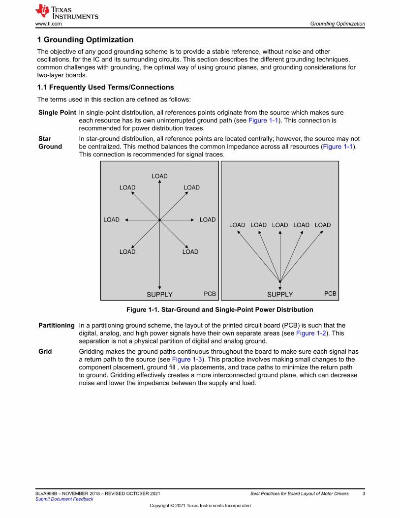
Single Point In single-point distribution, all references points originate from the source which makes sure each resource has its own uninterrupted ground path (see Figure 1-1). This connection is recommended for power distribution traces.
Star Ground
In star-ground distribution, all reference points are located centrally; however, the source may not be centralized. This method balances the common impedance across all resources (Figure 1-1). This connection is recommended for signal traces.
LOAD
SUPPLY PCB
LOAD LOAD LOAD LOADLOADLOAD
LOAD
LOADLOAD
LOAD LOAD
SUPPLY PCB
Figure 1-1. Star-Ground and Single-Point Power Distribution
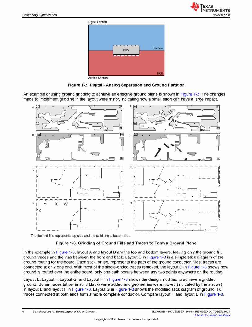
Partitioning In a partitioning ground scheme, the layout of the printed circuit board (PCB) is such that the digital, analog, and high power signals have their own separate areas (see Figure 1-2). This separation is not a physical partition of digital and analog ground.
Grid Gridding makes the ground paths continuous throughout the board to make sure each signal has a return path to the source (see Figure 1-3). This practice involves making small changes to the component placement, ground fill , via placements, and trace paths to minimize the return path to ground. Gridding effectively creates a more interconnected ground plane, which can decrease noise and lower the impedance between the supply and load.
www.ti.com Grounding Optimization
SLVA959B – NOVEMBER 2018 – REVISED OCTOBER 2021Submit Document Feedback
Best Practices for Board Layout of Motor Drivers 3
Copyright © 2021 Texas Instruments Incorporated
DRV
Analog Section
PCB
Partition
Digital Section
Figure 1-2. Digital - Analog Separation and Ground Partition
An example of using ground gridding to achieve an effective ground plane is shown in Figure 1-3. The changes made to implement gridding in the layout were minor, indicating how a small effort can have a large impact.
F
E
G
H
B
A
C
D
The dashed line represents top-side and the solid line is bottom-side.
Figure 1-3. Gridding of Ground Fills and Traces to Form a Ground Plane
In the example in Figure 1-3, layout A and layout B are the top and bottom layers, leaving only the ground fill, ground traces and the vias between the front and back. Layout C in Figure 1-3 is a simple stick diagram of the ground routing for the board. Each stick, or leg, represents the path of the ground conductor. Most traces are connected at only one end. With most of the single-ended traces removed, the layout D in Figure 1-3 shows how ground is routed over the entire board; only one path occurs between any two points anywhere on the routing.
Layout E, Layout F, Layout G, and Layout H in Figure 1-3 shows the design modified to achieve a gridded ground. Some traces (show in solid black) were added and geometries were moved (indicated by the arrows) in layout E and layout F in Figure 1-3. Layout G in Figure 1-3 shows the modified stick diagram of ground. Full traces connected at both ends form a more complete conductor. Compare layout H and layout D in Figure 1-3.
Grounding Optimization www.ti.com
4 Best Practices for Board Layout of Motor Drivers SLVA959B – NOVEMBER 2018 – REVISED OCTOBER 2021Submit Document Feedback
Copyright © 2021 Texas Instruments Incorporated
The gridding ground has created an extensive network of interconnections that creates the desired grid. The result is nearly as effective as an actual ground plane.
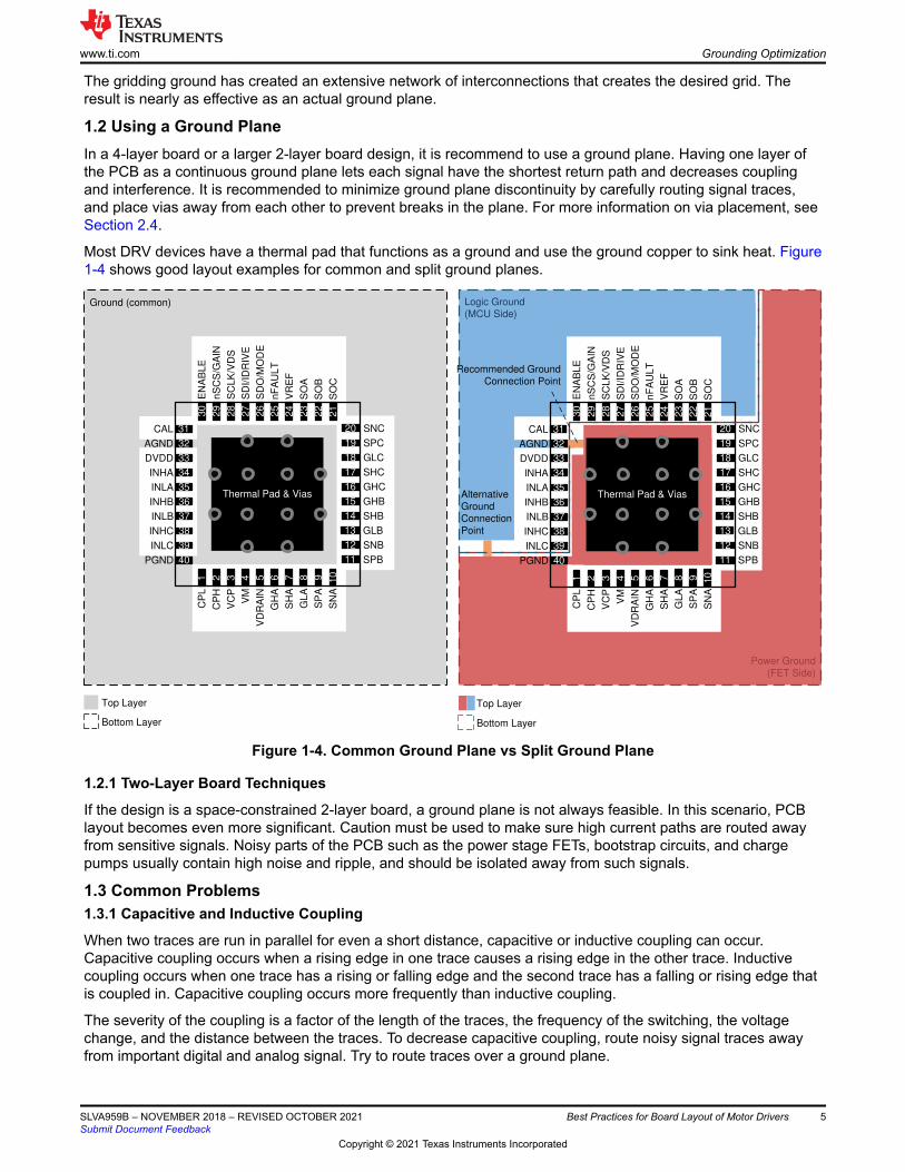
1.2 Using a Ground PlaneIn a 4-layer board or a larger 2-layer board design, it is recommend to use a ground plane. Having one layer of the PCB as a continuous ground plane lets each signal have the shortest return path and decreases coupling and interference. It is recommended to minimize ground plane discontinuity by carefully routing signal traces, and place vias away from each other to prevent breaks in the plane. For more information on via placement, see Section 2.4.
Most DRV devices have a thermal pad that functions as a ground and use the ground copper to sink heat. Figure 1-4 shows good layout examples for common and split ground planes.
CAL
AGND
DVDD
INHA
PGND
INLC
INLA
SO
B
SO
C
SD
I/ID
RIV
E
nF
AU
LT
nS
CS
/GA
IN
SC
LK
/VD
S
EN
AB
LE
SHC
GHC
GHB
SHB
GLB
SNC
SPC
GLC
SNB
SPB
CP
L
GH
A
SH
A
GL
A
SP
A
SN
A
VC
P
VM
VD
RA
IN
17
16
15
14
13
12
11
20
19
18
6 7 8 9 101 2 3 4 5
34
36
37
38
39
31
32
33
25
24
23
22
29
28
27
26
30
INLB
INHB
40
INHC
CP
H
35
21
SD
O/M
OD
E
VR
EF
SO
AGround (common)
Thermal Pad & Vias
Bottom Layer
Top Layer
CAL
AGND
DVDD
INHA
PGND
INLC
INLA
SO
B
SO
C
SD
I/ID
RIV
E
nF
AU
LT
nS
CS
/GA
IN
SC
LK
/VD
S
EN
AB
LE
SHC
GHC
GHB
SHB
GLB
SNC
SPC
GLC
SNB
SPB
CP
L
GH
A
SH
A
GL
A
SP
A
SN
A
VC
P
VM
VD
RA
IN
17
16
15
14
13
12
11
20
19
18
6 7 8 9 101 2 3 4 5
34
36
37
38
39
31
32
33
25
24
23
22
29
28
27
26
30
INLB
INHB
40
INHC
CP
H
35
21
SD
O/M
OD
E
VR
EF
SO
A
Logic Ground
(MCU Side)
Power Ground
(FET Side)
Alternative
Ground
Connection
Point
Recommended Ground
Connection Point
Thermal Pad & Vias
Bottom Layer
Top Layer
Figure 1-4. Common Ground Plane vs Split Ground Plane
1.2.1 Two-Layer Board Techniques
If the design is a space-constrained 2-layer board, a ground plane is not always feasible. In this scenario, PCB layout becomes even more significant. Caution must be used to make sure high current paths are routed away from sensitive signals. Noisy parts of the PCB such as the power stage FETs, bootstrap circuits, and charge pumps usually contain high noise and ripple, and should be isolated away from such signals.
1.3 Common Problems1.3.1 Capacitive and Inductive Coupling
When two traces are run in parallel for even a short distance, capacitive or inductive coupling can occur. Capacitive coupling occurs when a rising edge in one trace causes a rising edge in the other trace. Inductive coupling occurs when one trace has a rising or falling edge and the second trace has a falling or rising edge that is coupled in. Capacitive coupling occurs more frequently than inductive coupling.
The severity of the coupling is a factor of the length of the traces, the frequency of the switching, the voltage change, and the distance between the traces. To decrease capacitive coupling, route noisy signal traces away from important digital and analog signal. Try to route traces over a ground plane.
www.ti.com Grounding Optimization
SLVA959B – NOVEMBER 2018 – REVISED OCTOBER 2021Submit Document Feedback
Best Practices for Board Layout of Motor Drivers 5
Copyright © 2021 Texas Instruments Incorporated
In switching applications with a predriver, special care must be taken to make sure that the high-current carrying ground plane of the predriver is physically isolated from the ground plane of the remaining parts of the IC. These two grounds can be joined at the star-point or single-point grounding location as described in Section 1.1.
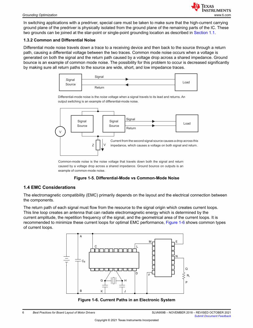
1.3.2 Common and Differential Noise
Differential mode noise travels down a trace to a receiving device and then back to the source through a return path, causing a differential voltage between the two traces. Common mode noise occurs when a voltage is generated on both the signal and the return path caused by a voltage drop across a shared impedance. Ground bounce is an example of common mode noise. The possibility for this problem to occur is decreased significantly by making sure all return paths to the source are wide, short, and low impedance traces.
Differential-mode noise is the voltage when a signal travels to its lead and returns. Annoise
output switching is an example of differential-mode noise.
Load
Common-mode noise is the noise voltage that travels down both the signal and return
caused by a voltage drop across a shared impedance. Ground bounce on outputs is an
example of common-mode noise.
Current from the second signal source causes a drop across this
impedance, which causes a voltage on both signal and return.
Signal
Source
Return
Signal
Return
Signal
LoadSignal
Source
Signal
Source
V
Z V
Figure 1-5. Differential-Mode vs Common-Mode Noise
1.4 EMC ConsiderationsThe electromagnetic compatibility (EMC) primarily depends on the layout and the electrical connection between the components.
The return path of each signal must flow from the resource to the signal origin which creates current loops. This line loop creates an antenna that can radiate electromagnetic energy which is determined by the current amplitude, the repetition frequency of the signal, and the geometrical area of the current loops. It is recommended to minimize these current loops for optimal EMC performance, Figure 1-6 shows common types of current loops.
M
A
C
CB
L
B K
G H
J
DF
E
N
Q
P
RL
Figure 1-6. Current Paths in an Electronic System
Grounding Optimization www.ti.com
6 Best Practices for Board Layout of Motor Drivers SLVA959B – NOVEMBER 2018 – REVISED OCTOBER 2021Submit Document Feedback
Copyright © 2021 Texas Instruments Incorporated

The supply lines in Figure 1-6 form loops A–C–D–B and A–E–F–B. The energy that the system requires to operate is conducted by these lines.
Loops L-M-F-D, N-Q-P-F, and G-H-J-K are formed by signals and controls. The area these lines enclose is usually small if those lines outside the system are not considered. However, these lines must be considered at high frequency because they often transmit signals which can affect EMC performance.
Current loops can also form when connectors, headers, or other components break up a ground plane. This causes high-frequency components of switching currents to travel further around the board and effectively create a large loop. This can also occur with vias and is highlighted in Section 3.2.2
www.ti.com Grounding Optimization
SLVA959B – NOVEMBER 2018 – REVISED OCTOBER 2021Submit Document Feedback
Best Practices for Board Layout of Motor Drivers 7
Copyright © 2021 Texas Instruments Incorporated
2 Thermal OverviewMotor drivers are not ideal devices, in real-world applications some of their power is dissipated internally as heat. The energy converted to heat must be dealt with before damage occurs to the driver. Proper PCB design can effectively remove heat generated by inefficiencies and keep the device at a recommended temperature.
2.1 PCB Conduction and ConvectionAn important consideration for motor driver thermal performance is the pathways which heat generated inside the device can dissipate. Three primary paths for heat to go from the die into lower temperature environments are:
• Encapsulation material• Bond wires• Thermal pad
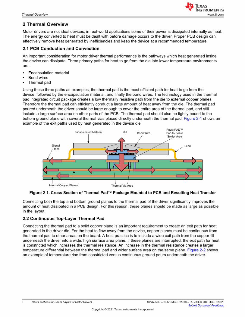
Using these three paths as examples, the thermal pad is the most efficient path for heat to go from the device, followed by the encapsulation material, and finally the bond wires. The technology used in the thermal pad integrated circuit package creates a low thermally resistive path from the die to external copper planes. Therefore the thermal pad can efficiently conduct a large amount of heat away from the die. The thermal pad poured underneath the driver should be large enough to cover the entire area of the thermal pad, and still include a large surface area on other parts of the PCB. The thermal pad should also be tightly bound to the bottom ground plane with several thermal vias placed directly underneath the thermal pad. Figure 2-1 shows an example of the exit paths used by heat generated in the device die.
Die Bond Wire
3RZHU3$'�
Pad-to-Board
Solder Area
Lead
Thermal Via Area
Encapsulated Material
Signal
Trace
Internal Copper Planes
Figure 2-1. Cross Section of Thermal Pad™ Package Mounted to PCB and Resulting Heat Transfer
Connecting both the top and bottom ground planes to the thermal pad of the driver significantly improves the amount of heat dissipated in a PCB design. For this reason, these planes should be made as large as possible in the layout.
2.2 Continuous Top-Layer Thermal PadConnecting the thermal pad to a solid copper plane is an important requirement to create an exit path for heat generated in the driver die. For the heat to flow away from the device, copper planes must be continuous from the thermal pad to other areas on the board. A best practice is to include a wide exit path from the copper fill underneath the driver into a wide, high surface area plane. If these planes are interrupted, the exit path for heat is constricted which increases the thermal resistance. An increase in the thermal resistance creates a larger temperature differential between the thermal pad and wider surface area on the same plane. Figure 2-2 shows an example of temperature rise from constricted versus continuous ground pours underneath the driver.
Thermal Overview www.ti.com
8 Best Practices for Board Layout of Motor Drivers SLVA959B – NOVEMBER 2018 – REVISED OCTOBER 2021Submit Document Feedback
Copyright © 2021 Texas Instruments Incorporated
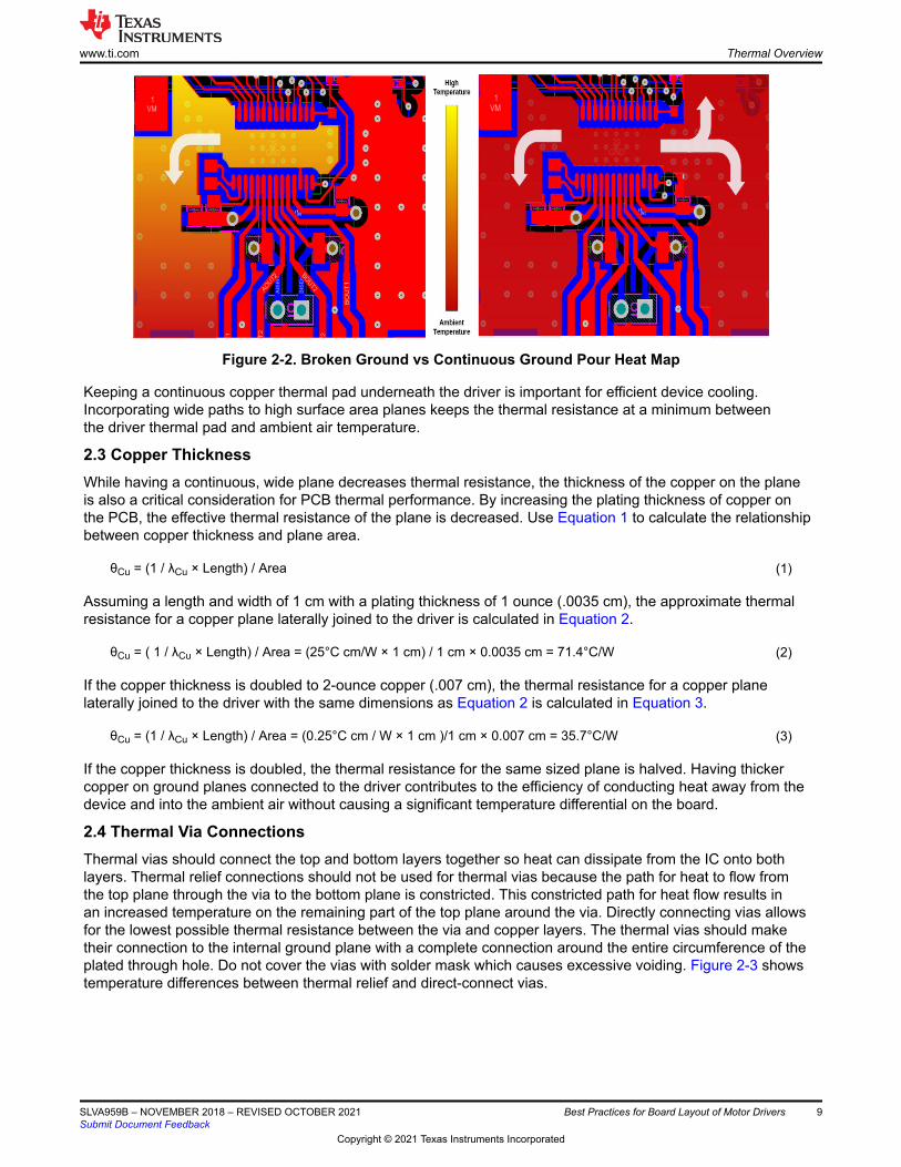
Figure 2-2. Broken Ground vs Continuous Ground Pour Heat Map
Keeping a continuous copper thermal pad underneath the driver is important for efficient device cooling. Incorporating wide paths to high surface area planes keeps the thermal resistance at a minimum between the driver thermal pad and ambient air temperature.
2.3 Copper ThicknessWhile having a continuous, wide plane decreases thermal resistance, the thickness of the copper on the plane is also a critical consideration for PCB thermal performance. By increasing the plating thickness of copper on the PCB, the effective thermal resistance of the plane is decreased. Use Equation 1 to calculate the relationship between copper thickness and plane area.
θCu = (1 / λCu × Length) / Area (1)
Assuming a length and width of 1 cm with a plating thickness of 1 ounce (.0035 cm), the approximate thermal resistance for a copper plane laterally joined to the driver is calculated in Equation 2.
θCu = ( 1 / λCu × Length) / Area = (25°C cm/W × 1 cm) / 1 cm × 0.0035 cm = 71.4°C/W (2)
If the copper thickness is doubled to 2-ounce copper (.007 cm), the thermal resistance for a copper plane laterally joined to the driver with the same dimensions as Equation 2 is calculated in Equation 3.
θCu = (1 / λCu × Length) / Area = (0.25°C cm / W × 1 cm )/1 cm × 0.007 cm = 35.7°C/W (3)
If the copper thickness is doubled, the thermal resistance for the same sized plane is halved. Having thicker copper on ground planes connected to the driver contributes to the efficiency of conducting heat away from the device and into the ambient air without causing a significant temperature differential on the board.
2.4 Thermal Via ConnectionsThermal vias should connect the top and bottom layers together so heat can dissipate from the IC onto both layers. Thermal relief connections should not be used for thermal vias because the path for heat to flow from the top plane through the via to the bottom plane is constricted. This constricted path for heat flow results in an increased temperature on the remaining part of the top plane around the via. Directly connecting vias allows for the lowest possible thermal resistance between the via and copper layers. The thermal vias should make their connection to the internal ground plane with a complete connection around the entire circumference of the plated through hole. Do not cover the vias with solder mask which causes excessive voiding. Figure 2-3 shows temperature differences between thermal relief and direct-connect vias.
www.ti.com Thermal Overview
SLVA959B – NOVEMBER 2018 – REVISED OCTOBER 2021Submit Document Feedback
Best Practices for Board Layout of Motor Drivers 9
Copyright © 2021 Texas Instruments Incorporated
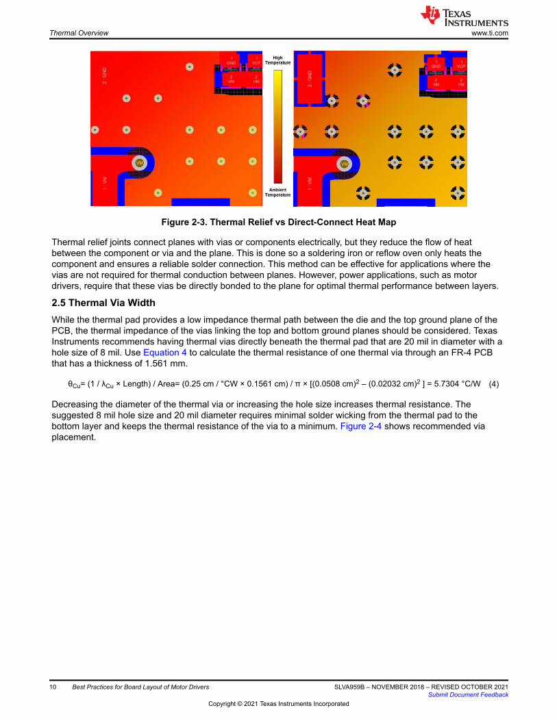
Figure 2-3. Thermal Relief vs Direct-Connect Heat Map
Thermal relief joints connect planes with vias or components electrically, but they reduce the flow of heat between the component or via and the plane. This is done so a soldering iron or reflow oven only heats the component and ensures a reliable solder connection. This method can be effective for applications where the vias are not required for thermal conduction between planes. However, power applications, such as motor drivers, require that these vias be directly bonded to the plane for optimal thermal performance between layers.
2.5 Thermal Via WidthWhile the thermal pad provides a low impedance thermal path between the die and the top ground plane of the PCB, the thermal impedance of the vias linking the top and bottom ground planes should be considered. Texas Instruments recommends having thermal vias directly beneath the thermal pad that are 20 mil in diameter with a hole size of 8 mil. Use Equation 4 to calculate the thermal resistance of one thermal via through an FR-4 PCB that has a thickness of 1.561 mm.
θCu= (1 / λCu × Length) / Area= (0.25 cm / °CW × 0.1561 cm) / π × [(0.0508 cm)2 – (0.02032 cm)2 ] = 5.7304 °C/W (4)
Decreasing the diameter of the thermal via or increasing the hole size increases thermal resistance. The suggested 8 mil hole size and 20 mil diameter requires minimal solder wicking from the thermal pad to the bottom layer and keeps the thermal resistance of the via to a minimum. Figure 2-4 shows recommended via placement.
Thermal Overview www.ti.com
10 Best Practices for Board Layout of Motor Drivers SLVA959B – NOVEMBER 2018 – REVISED OCTOBER 2021Submit Document Feedback
Copyright © 2021 Texas Instruments Incorporated
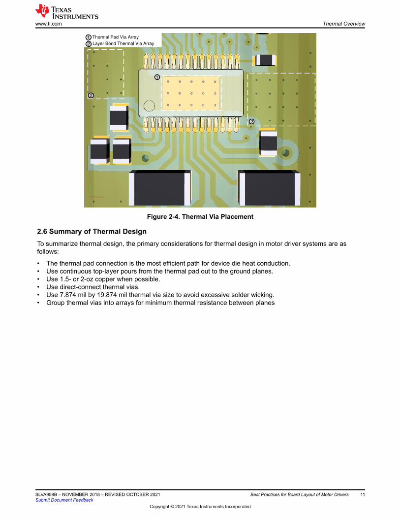
Thermal Pad Via Array
Layer Bond Thermal Via Array
1
2
2
1
2
Figure 2-4. Thermal Via Placement
2.6 Summary of Thermal DesignTo summarize thermal design, the primary considerations for thermal design in motor driver systems are as follows:
• The thermal pad connection is the most efficient path for device die heat conduction.• Use continuous top-layer pours from the thermal pad out to the ground planes.• Use 1.5- or 2-oz copper when possible.• Use direct-connect thermal vias.• Use 7.874 mil by 19.874 mil thermal via size to avoid excessive solder wicking.• Group thermal vias into arrays for minimum thermal resistance between planes
www.ti.com Thermal Overview
SLVA959B – NOVEMBER 2018 – REVISED OCTOBER 2021Submit Document Feedback
Best Practices for Board Layout of Motor Drivers 11
Copyright © 2021 Texas Instruments Incorporated
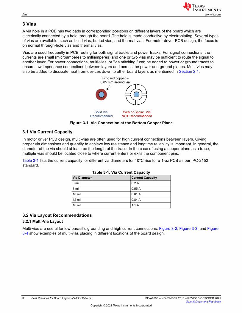
3 ViasA via hole in a PCB has two pads in corresponding positions on different layers of the board which are electrically connected by a hole through the board. The hole is made conductive by electroplating. Several types of vias are available, such as blind vias, buried vias, and thermal vias. For motor driver PCB design, the focus is on normal through-hole vias and thermal vias.
Vias are used frequently in PCB routing for both signal tracks and power tracks. For signal connections, the currents are small (microamperes to milliamperes) and one or two vias may be sufficient to route the signal to another layer. For power connections, multi-vias, or "via stitching," can be added to power or ground traces to ensure low impedance connections between layers and across the power and ground planes. Multi-vias may also be added to dissipate heat from devices down to other board layers as mentioned in Section 2.4.
Web or Spoke Via
NOT Recommended
Solid Via
Recommended
Exposed copper –
0.05 mm around via
Figure 3-1. Via Connection at the Bottom Copper Plane
3.1 Via Current CapacityIn motor driver PCB design, multi-vias are often used for high current connections between layers. Giving proper via dimensions and quantity to achieve low resistance and longtime reliability is important. In general, the diameter of the via should at least be the length of the trace. In the case of using a copper plane as a trace, multiple vias should be located close to where current enters or exits the component pins.
Table 3-1 lists the current capacity for different via diameters for 10°C rise for a 1-oz PCB as per IPC-2152 standard.
Table 3-1. Via Current CapacityVia Diameter Current Capacity6 mil 0.2 A
8 mil 0.55 A
10 mil 0.81 A
12 mil 0.84 A
16 mil 1.1 A
3.2 Via Layout Recommendations3.2.1 Multi-Via Layout
Multi-vias are useful for low parasitic grounding and high current connections. Figure 3-2, Figure 3-3, and Figure 3-4 show examples of multi-vias placing in different locations of the board design.
Vias www.ti.com
12 Best Practices for Board Layout of Motor Drivers SLVA959B – NOVEMBER 2018 – REVISED OCTOBER 2021Submit Document Feedback
Copyright © 2021 Texas Instruments Incorporated
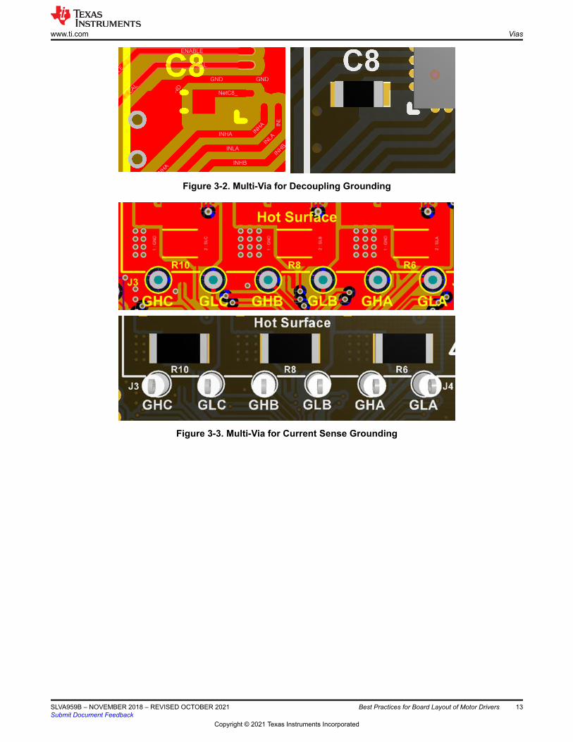
Figure 3-2. Multi-Via for Decoupling Grounding
Figure 3-3. Multi-Via for Current Sense Grounding
www.ti.com Vias
SLVA959B – NOVEMBER 2018 – REVISED OCTOBER 2021Submit Document Feedback
Best Practices for Board Layout of Motor Drivers 13
Copyright © 2021 Texas Instruments Incorporated
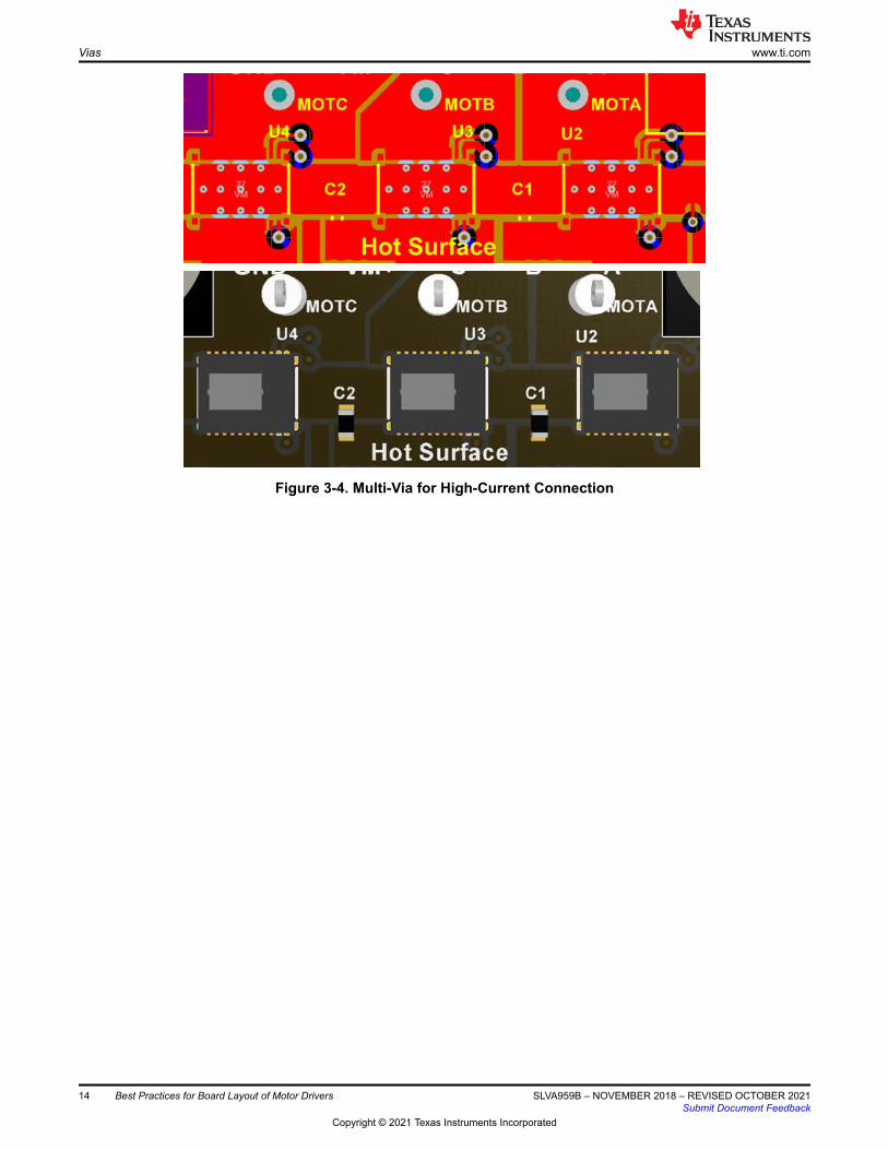
Figure 3-4. Multi-Via for High-Current Connection
Vias www.ti.com
14 Best Practices for Board Layout of Motor Drivers SLVA959B – NOVEMBER 2018 – REVISED OCTOBER 2021Submit Document Feedback
Copyright © 2021 Texas Instruments Incorporated
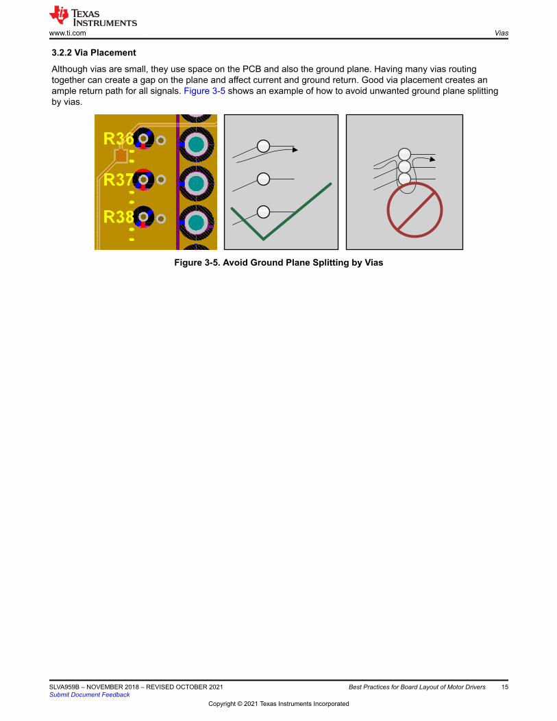
3.2.2 Via Placement
Although vias are small, they use space on the PCB and also the ground plane. Having many vias routing together can create a gap on the plane and affect current and ground return. Good via placement creates an ample return path for all signals. Figure 3-5 shows an example of how to avoid unwanted ground plane splitting by vias.
Figure 3-5. Avoid Ground Plane Splitting by Vias
www.ti.com Vias
SLVA959B – NOVEMBER 2018 – REVISED OCTOBER 2021Submit Document Feedback
Best Practices for Board Layout of Motor Drivers 15
Copyright © 2021 Texas Instruments Incorporated
4 General Routing TechniquesFollow these general routing techniques when doing a motor driver PCB design:
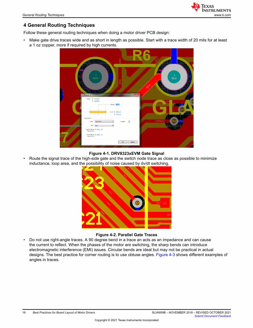
• Make gate drive traces wide and as short in length as possible. Start with a trace width of 20 mils for at least a 1 oz copper, more if required by high currents.
Figure 4-1. DRV8323xEVM Gate Signal• Route the signal trace of the high-side gate and the switch node trace as close as possible to minimize
inductance, loop area, and the possibility of noise caused by dv/dt switching.
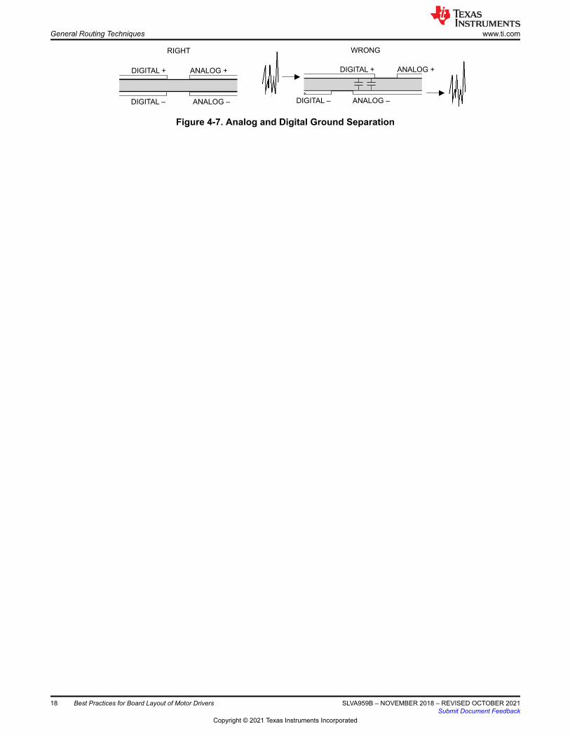
Figure 4-2. Parallel Gate Traces• Do not use right-angle traces. A 90 degree bend in a trace an acts as an impedance and can cause
the current to reflect. When the phases of the motor are switching, the sharp bends can introduce electromagnetic interference (EMI) issues. Circular bends are ideal but may not be practical in actual designs. The best practice for corner routing is to use obtuse angles. Figure 4-3 shows different examples of angles in traces.
General Routing Techniques www.ti.com
16 Best Practices for Board Layout of Motor Drivers SLVA959B – NOVEMBER 2018 – REVISED OCTOBER 2021Submit Document Feedback
Copyright © 2021 Texas Instruments Incorporated
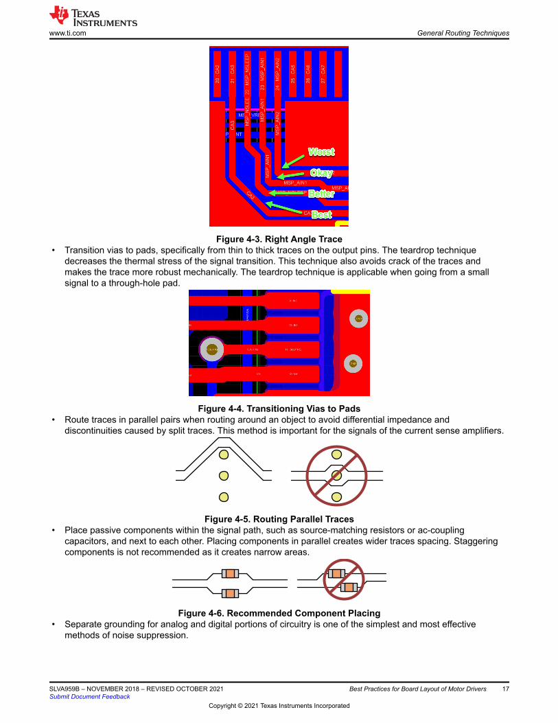
Figure 4-3. Right Angle Trace• Transition vias to pads, specifically from thin to thick traces on the output pins. The teardrop technique
decreases the thermal stress of the signal transition. This technique also avoids crack of the traces and makes the trace more robust mechanically. The teardrop technique is applicable when going from a small signal to a through-hole pad.
Figure 4-4. Transitioning Vias to Pads• Route traces in parallel pairs when routing around an object to avoid differential impedance and
discontinuities caused by split traces. This method is important for the signals of the current sense amplifiers.
Figure 4-5. Routing Parallel Traces• Place passive components within the signal path, such as source-matching resistors or ac-coupling
capacitors, and next to each other. Placing components in parallel creates wider traces spacing. Staggering components is not recommended as it creates narrow areas.
Figure 4-6. Recommended Component Placing• Separate grounding for analog and digital portions of circuitry is one of the simplest and most effective
methods of noise suppression.
www.ti.com General Routing Techniques
SLVA959B – NOVEMBER 2018 – REVISED OCTOBER 2021Submit Document Feedback
Best Practices for Board Layout of Motor Drivers 17
Copyright © 2021 Texas Instruments Incorporated
RIGHT
ANALOG +
ANALOG –DIGITAL –
DIGITAL +ANALOG +
ANALOG –DIGITAL –
DIGITAL +
WRONG
Figure 4-7. Analog and Digital Ground Separation
General Routing Techniques www.ti.com
18 Best Practices for Board Layout of Motor Drivers SLVA959B – NOVEMBER 2018 – REVISED OCTOBER 2021Submit Document Feedback
Copyright © 2021 Texas Instruments Incorporated
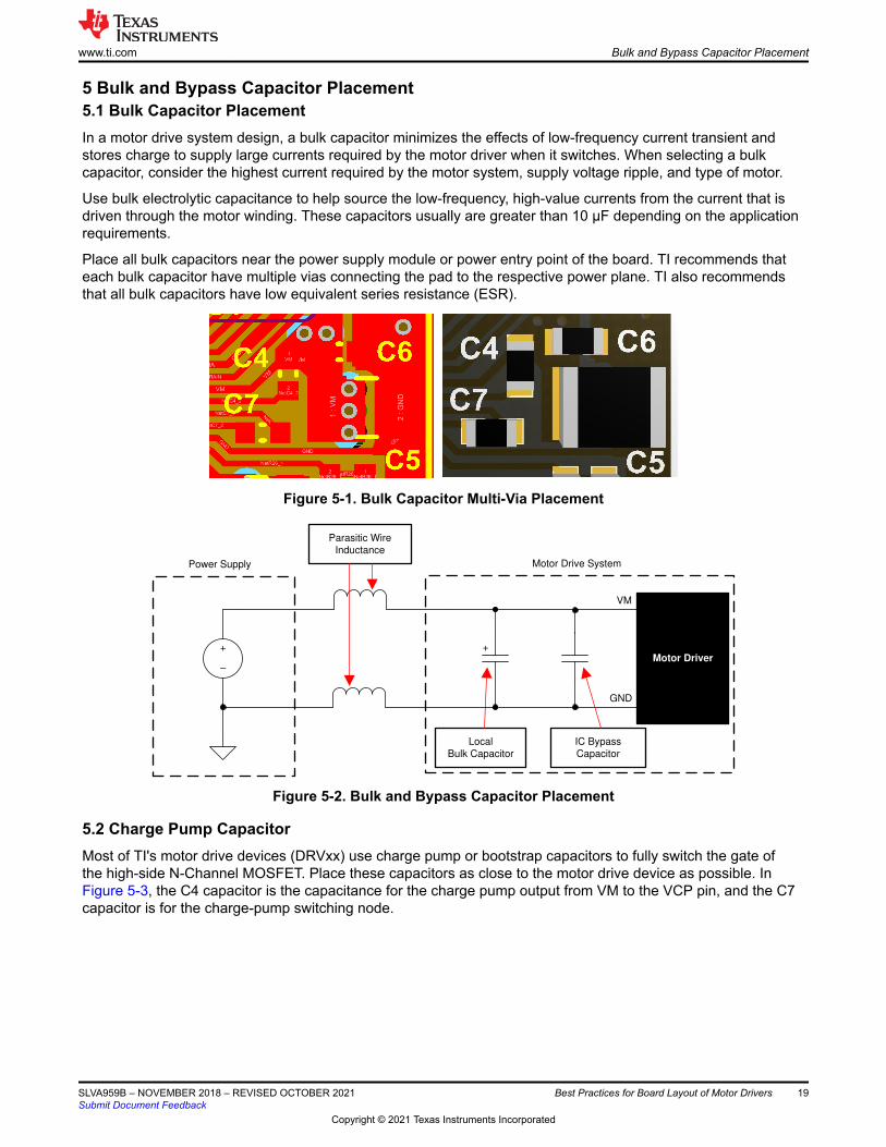
5 Bulk and Bypass Capacitor Placement5.1 Bulk Capacitor PlacementIn a motor drive system design, a bulk capacitor minimizes the effects of low-frequency current transient and stores charge to supply large currents required by the motor driver when it switches. When selecting a bulk capacitor, consider the highest current required by the motor system, supply voltage ripple, and type of motor.
Use bulk electrolytic capacitance to help source the low-frequency, high-value currents from the current that is driven through the motor winding. These capacitors usually are greater than 10 µF depending on the application requirements.
Place all bulk capacitors near the power supply module or power entry point of the board. TI recommends that each bulk capacitor have multiple vias connecting the pad to the respective power plane. TI also recommends that all bulk capacitors have low equivalent series resistance (ESR).
Figure 5-1. Bulk Capacitor Multi-Via Placement
Local
Bulk Capacitor
Parasitic Wire
Inductance
+
±
Motor Driver
Power Supply Motor Drive System
VM
GND
+
IC Bypass
Capacitor
Figure 5-2. Bulk and Bypass Capacitor Placement
5.2 Charge Pump CapacitorMost of TI's motor drive devices (DRVxx) use charge pump or bootstrap capacitors to fully switch the gate of the high-side N-Channel MOSFET. Place these capacitors as close to the motor drive device as possible. In Figure 5-3, the C4 capacitor is the capacitance for the charge pump output from VM to the VCP pin, and the C7 capacitor is for the charge-pump switching node.
www.ti.com Bulk and Bypass Capacitor Placement
SLVA959B – NOVEMBER 2018 – REVISED OCTOBER 2021Submit Document Feedback
Best Practices for Board Layout of Motor Drivers 19
Copyright © 2021 Texas Instruments Incorporated
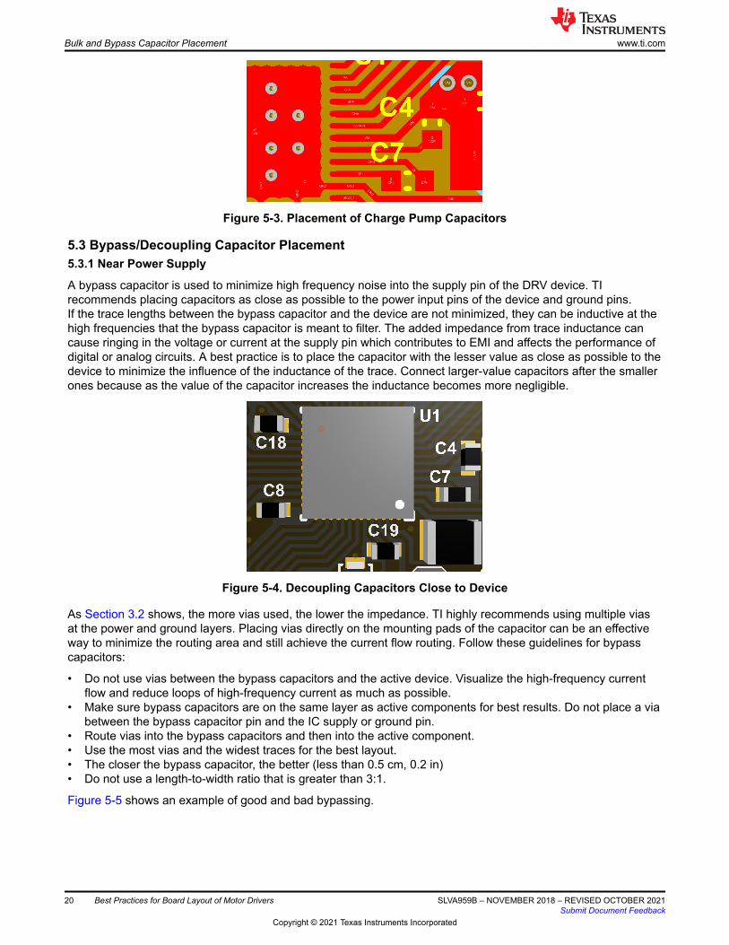
Figure 5-3. Placement of Charge Pump Capacitors
5.3 Bypass/Decoupling Capacitor Placement5.3.1 Near Power Supply
A bypass capacitor is used to minimize high frequency noise into the supply pin of the DRV device. TI recommends placing capacitors as close as possible to the power input pins of the device and ground pins. If the trace lengths between the bypass capacitor and the device are not minimized, they can be inductive at the high frequencies that the bypass capacitor is meant to filter. The added impedance from trace inductance can cause ringing in the voltage or current at the supply pin which contributes to EMI and affects the performance of digital or analog circuits. A best practice is to place the capacitor with the lesser value as close as possible to the device to minimize the influence of the inductance of the trace. Connect larger-value capacitors after the smaller ones because as the value of the capacitor increases the inductance becomes more negligible.
Figure 5-4. Decoupling Capacitors Close to Device
As Section 3.2 shows, the more vias used, the lower the impedance. TI highly recommends using multiple vias at the power and ground layers. Placing vias directly on the mounting pads of the capacitor can be an effective way to minimize the routing area and still achieve the current flow routing. Follow these guidelines for bypass capacitors:
• Do not use vias between the bypass capacitors and the active device. Visualize the high-frequency current flow and reduce loops of high-frequency current as much as possible.
• Make sure bypass capacitors are on the same layer as active components for best results. Do not place a via between the bypass capacitor pin and the IC supply or ground pin.
• Route vias into the bypass capacitors and then into the active component.• Use the most vias and the widest traces for the best layout.• The closer the bypass capacitor, the better (less than 0.5 cm, 0.2 in)• Do not use a length-to-width ratio that is greater than 3:1.
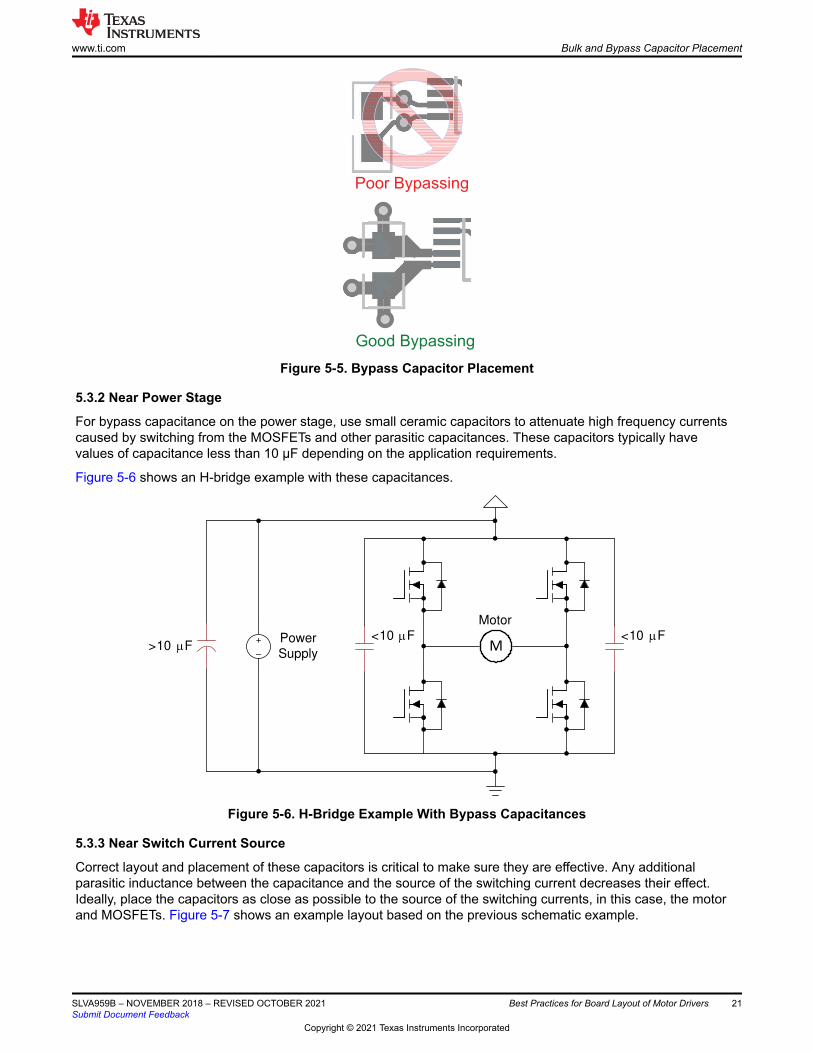
Figure 5-5 shows an example of good and bad bypassing.
Bulk and Bypass Capacitor Placement www.ti.com
20 Best Practices for Board Layout of Motor Drivers SLVA959B – NOVEMBER 2018 – REVISED OCTOBER 2021Submit Document Feedback
Copyright © 2021 Texas Instruments Incorporated
Poor Bypassing
Good Bypassing
Figure 5-5. Bypass Capacitor Placement
5.3.2 Near Power Stage
For bypass capacitance on the power stage, use small ceramic capacitors to attenuate high frequency currents caused by switching from the MOSFETs and other parasitic capacitances. These capacitors typically have values of capacitance less than 10 µF depending on the application requirements.
Figure 5-6 shows an H-bridge example with these capacitances.
MPower
Supply
Motor
>10 PF<10 PF <10 PF+
±
Figure 5-6. H-Bridge Example With Bypass Capacitances
5.3.3 Near Switch Current Source
Correct layout and placement of these capacitors is critical to make sure they are effective. Any additional parasitic inductance between the capacitance and the source of the switching current decreases their effect. Ideally, place the capacitors as close as possible to the source of the switching currents, in this case, the motor and MOSFETs. Figure 5-7 shows an example layout based on the previous schematic example.
www.ti.com Bulk and Bypass Capacitor Placement
SLVA959B – NOVEMBER 2018 – REVISED OCTOBER 2021Submit Document Feedback
Best Practices for Board Layout of Motor Drivers 21
Copyright © 2021 Texas Instruments Incorporated
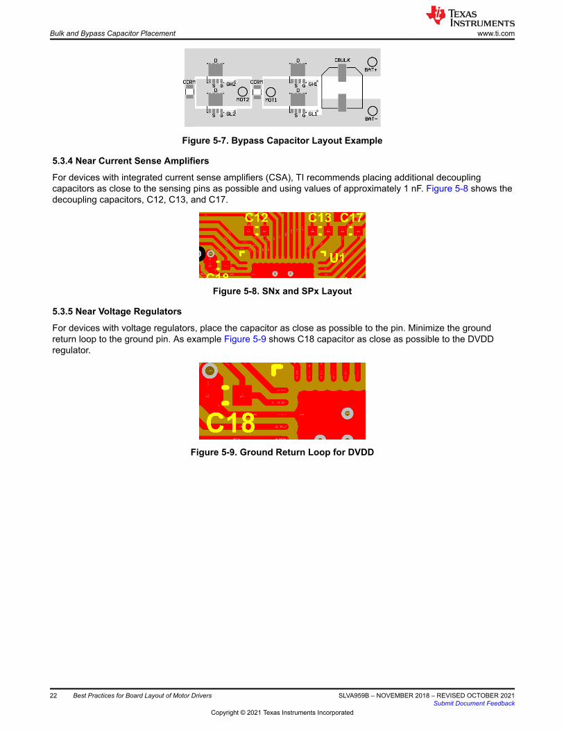
Figure 5-7. Bypass Capacitor Layout Example
5.3.4 Near Current Sense Amplifiers
For devices with integrated current sense amplifiers (CSA), TI recommends placing additional decoupling capacitors as close to the sensing pins as possible and using values of approximately 1 nF. Figure 5-8 shows the decoupling capacitors, C12, C13, and C17.
Figure 5-8. SNx and SPx Layout
5.3.5 Near Voltage Regulators
For devices with voltage regulators, place the capacitor as close as possible to the pin. Minimize the ground return loop to the ground pin. As example Figure 5-9 shows C18 capacitor as close as possible to the DVDD regulator.
Figure 5-9. Ground Return Loop for DVDD
Bulk and Bypass Capacitor Placement www.ti.com
22 Best Practices for Board Layout of Motor Drivers SLVA959B – NOVEMBER 2018 – REVISED OCTOBER 2021Submit Document Feedback
Copyright © 2021 Texas Instruments Incorporated
6 MOSFET Placement and Power Stage RoutingPlacement of the gate driver and power MOSFETs is critical for correct functionality and optimal performance in for pre-driver motor drive solutions. For motor drivers with integrated MOSFETs, such as the DRV8870, DRV8313, DRV10987, DRV10983-Q1, and DRV8873-Q1, the proper routing is already done internally. For gate drivers, such as the DRV8701, DRV8304, DRV8306, DRV8323, DRV8343-Q1, and DRV8353, carefully planning the layout of the PCB and the placement of the power MOSFETs is important. The following sections describe some common MOSFET topologies and present basic layout examples using common motor drive architectures.
6.1 Common Power MOSFET PackagesThis section describes some of the common package types of N-channel power MOSFETs. The majority of power MOSFETs have one of these four options. By understanding the package types, their dimensions, and pinouts, the PCB can be better designed for an optimal solution.
The symbol in Figure 6-1 represents an N-channel power MOSFET. While the MOSFET is a four-terminal device with source, gate, drain, and body, the body terminal is usually to the source terminal.
Drain
Source
Gate
Figure 6-1. N-Channel Power MOSFET Symbol
The MOSFET packages have a direct connection with power stage and thermal dissipation. Different packages have difference routing rules.
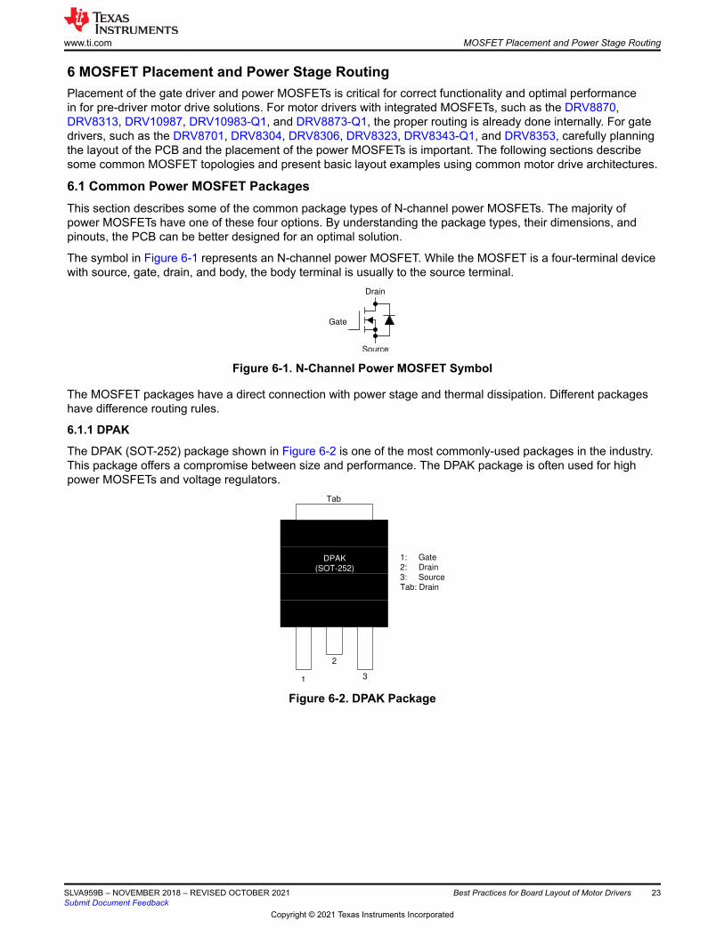
6.1.1 DPAK
The DPAK (SOT-252) package shown in Figure 6-2 is one of the most commonly-used packages in the industry. This package offers a compromise between size and performance. The DPAK package is often used for high power MOSFETs and voltage regulators.
DPAK
(SOT-252)
1
2
3
1: Gate
2: Drain
3: Source
Tab: Drain
Tab
Figure 6-2. DPAK Package
www.ti.com MOSFET Placement and Power Stage Routing
SLVA959B – NOVEMBER 2018 – REVISED OCTOBER 2021Submit Document Feedback
Best Practices for Board Layout of Motor Drivers 23
Copyright © 2021 Texas Instruments Incorporated
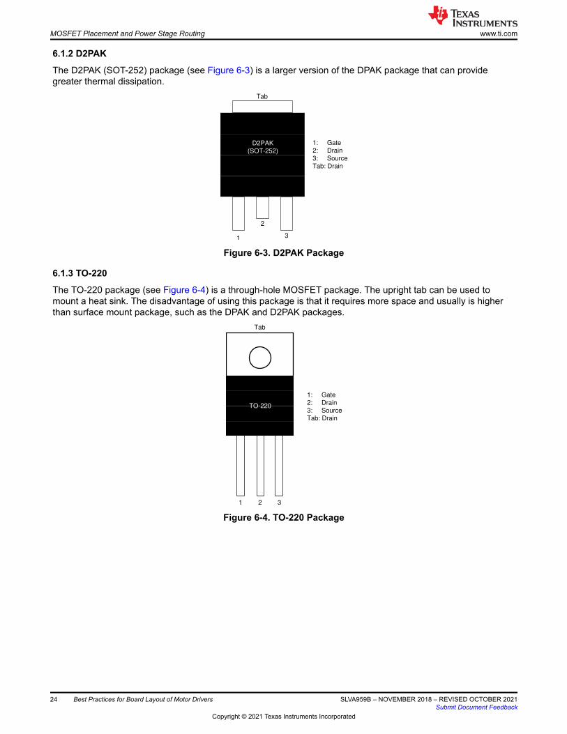
6.1.2 D2PAK
The D2PAK (SOT-252) package (see Figure 6-3) is a larger version of the DPAK package that can provide greater thermal dissipation.
D2PAK
(SOT-252)
1
2
3
1: Gate
2: Drain
3: Source
Tab: Drain
Tab
Figure 6-3. D2PAK Package
6.1.3 TO-220
The TO-220 package (see Figure 6-4) is a through-hole MOSFET package. The upright tab can be used to mount a heat sink. The disadvantage of using this package is that it requires more space and usually is higher than surface mount package, such as the DPAK and D2PAK packages.
TO-220
Tab
1 2 3
1: Gate
2: Drain
3: Source
Tab: Drain
Figure 6-4. TO-220 Package
MOSFET Placement and Power Stage Routing www.ti.com
24 Best Practices for Board Layout of Motor Drivers SLVA959B – NOVEMBER 2018 – REVISED OCTOBER 2021Submit Document Feedback
Copyright © 2021 Texas Instruments Incorporated
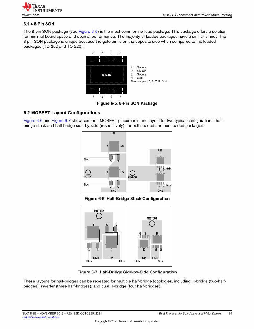
6.1.4 8-Pin SON
The 8-pin SON package (see Figure 6-5) is the most common no-lead package. This package offers a solution for minimal board space and optimal performance. The majority of leaded packages have a similar pinout. The 8-pin SON package is unique because the gate pin is on the opposite side when compared to the leaded packages (TO-252 and TO-220).
8-SON
1 2 3
1: Source
2: Source
3: Source4: Gate
Thermal pad, 5, 6, 7, 8: Drain
4
8 7 6 5
Figure 6-5. 8-Pin SON Package
6.2 MOSFET Layout ConfigurationsFigure 6-6 and Figure 6-7 show common MOSFET placements and layout for two typical configurations; half-bridge stack and half-bridge side-by-side (respectively), for both leaded and non-leaded packages.
Figure 6-6. Half-Bridge Stack Configuration
Figure 6-7. Half-Bridge Side-by-Side Configuration
These layouts for half-bridges can be repeated for multiple half-bridge topologies, including H-bridge (two-half-bridges), inverter (three half-bridges), and dual H-bridge (four half-bridges).
www.ti.com MOSFET Placement and Power Stage Routing
SLVA959B – NOVEMBER 2018 – REVISED OCTOBER 2021Submit Document Feedback
Best Practices for Board Layout of Motor Drivers 25
Copyright © 2021 Texas Instruments Incorporated
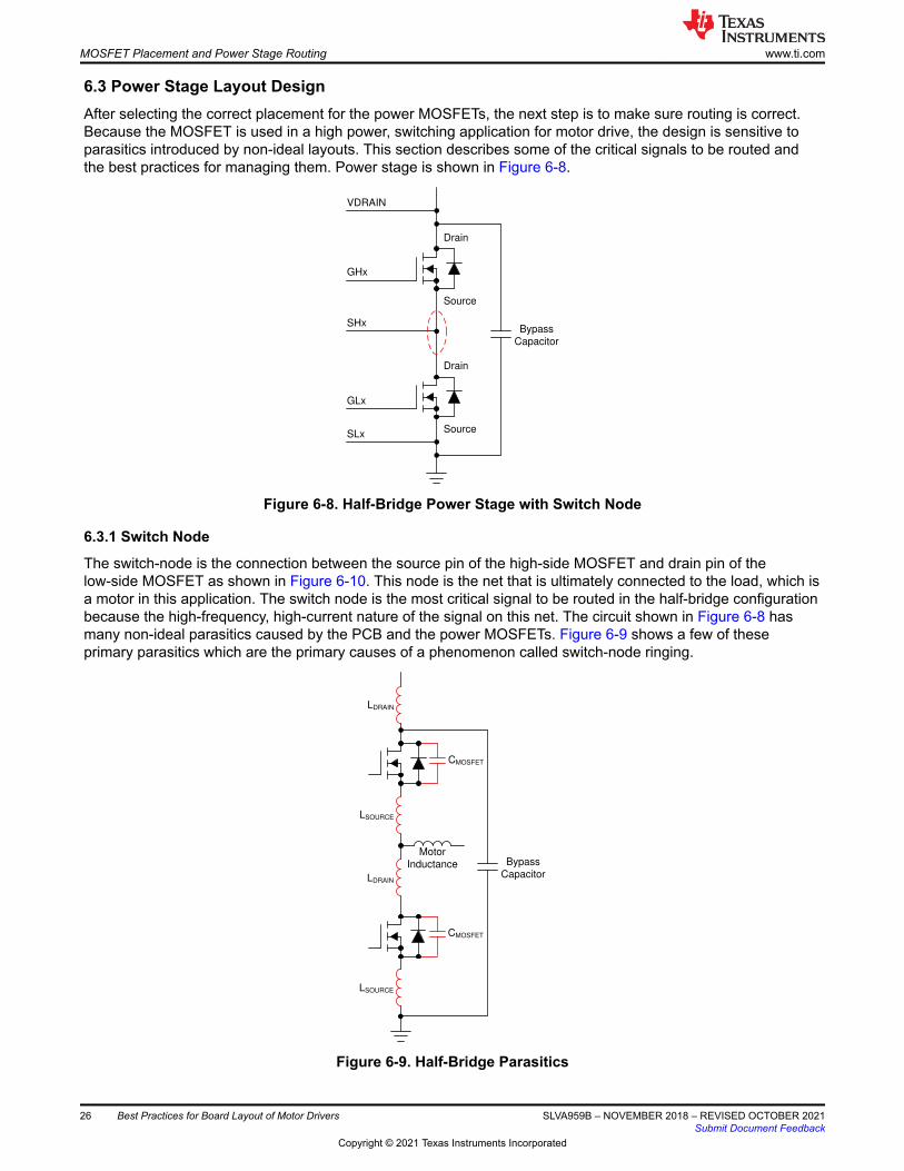
6.3 Power Stage Layout DesignAfter selecting the correct placement for the power MOSFETs, the next step is to make sure routing is correct. Because the MOSFET is used in a high power, switching application for motor drive, the design is sensitive to parasitics introduced by non-ideal layouts. This section describes some of the critical signals to be routed and the best practices for managing them. Power stage is shown in Figure 6-8.
Drain
Source
Drain
Source
Bypass
Capacitor
VDRAIN
GHx
SHx
GLx
SLx
Figure 6-8. Half-Bridge Power Stage with Switch Node
6.3.1 Switch Node
The switch-node is the connection between the source pin of the high-side MOSFET and drain pin of the low-side MOSFET as shown in Figure 6-10. This node is the net that is ultimately connected to the load, which is a motor in this application. The switch node is the most critical signal to be routed in the half-bridge configuration because the high-frequency, high-current nature of the signal on this net. The circuit shown in Figure 6-8 has many non-ideal parasitics caused by the PCB and the power MOSFETs. Figure 6-9 shows a few of these primary parasitics which are the primary causes of a phenomenon called switch-node ringing.
Bypass
Capacitor
CMOSFET
LDRAIN
LSOURCE
CMOSFET
LDRAIN
LSOURCE
Motor
Inductance
Figure 6-9. Half-Bridge Parasitics
MOSFET Placement and Power Stage Routing www.ti.com
26 Best Practices for Board Layout of Motor Drivers SLVA959B – NOVEMBER 2018 – REVISED OCTOBER 2021Submit Document Feedback
Copyright © 2021 Texas Instruments Incorporated
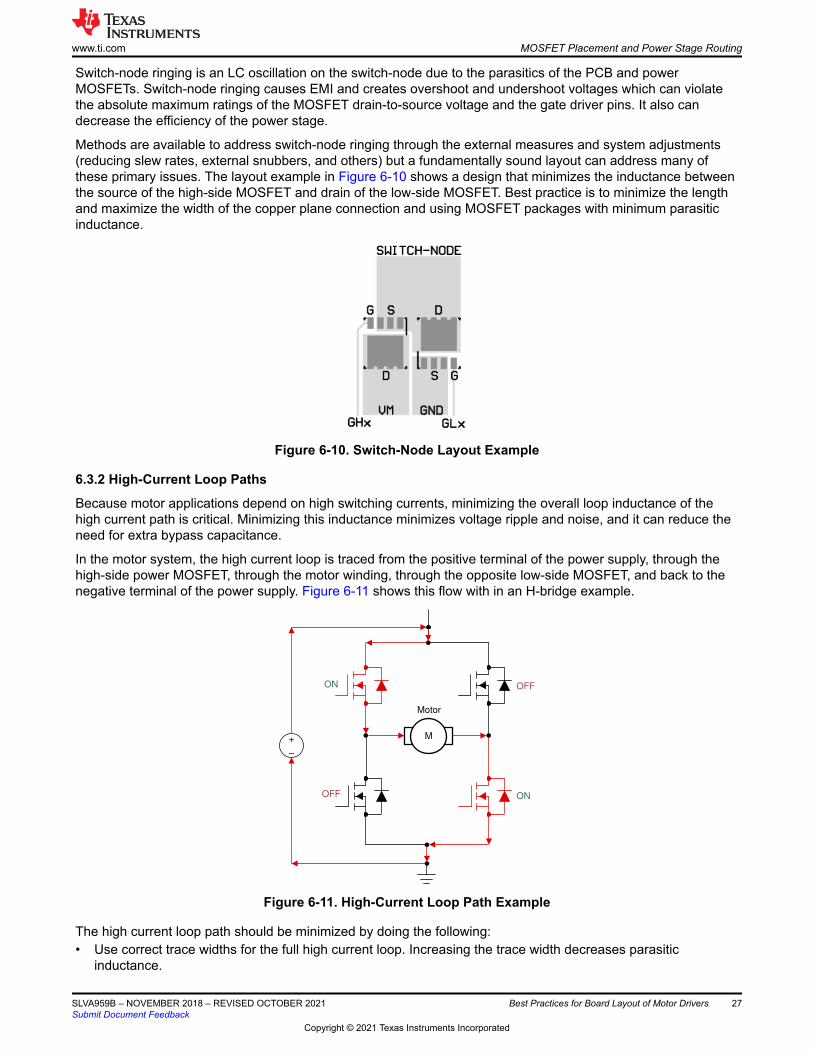
Switch-node ringing is an LC oscillation on the switch-node due to the parasitics of the PCB and power MOSFETs. Switch-node ringing causes EMI and creates overshoot and undershoot voltages which can violate the absolute maximum ratings of the MOSFET drain-to-source voltage and the gate driver pins. It also can decrease the efficiency of the power stage.
Methods are available to address switch-node ringing through the external measures and system adjustments (reducing slew rates, external snubbers, and others) but a fundamentally sound layout can address many of these primary issues. The layout example in Figure 6-10 shows a design that minimizes the inductance between the source of the high-side MOSFET and drain of the low-side MOSFET. Best practice is to minimize the length and maximize the width of the copper plane connection and using MOSFET packages with minimum parasitic inductance.
Figure 6-10. Switch-Node Layout Example
6.3.2 High-Current Loop Paths
Because motor applications depend on high switching currents, minimizing the overall loop inductance of the high current path is critical. Minimizing this inductance minimizes voltage ripple and noise, and it can reduce the need for extra bypass capacitance.
In the motor system, the high current loop is traced from the positive terminal of the power supply, through the high-side power MOSFET, through the motor winding, through the opposite low-side MOSFET, and back to the negative terminal of the power supply. Figure 6-11 shows this flow with in an H-bridge example.
OFF
OFF
ON
ON
M
Motor
+
±
Figure 6-11. High-Current Loop Path Example
The high current loop path should be minimized by doing the following:• Use correct trace widths for the full high current loop. Increasing the trace width decreases parasitic
inductance.
www.ti.com MOSFET Placement and Power Stage Routing
SLVA959B – NOVEMBER 2018 – REVISED OCTOBER 2021Submit Document Feedback
Best Practices for Board Layout of Motor Drivers 27
Copyright © 2021 Texas Instruments Incorporated
• Use correct placement to minimize the distance between components. Decreasing the trace length decreases parasitic inductance.
• Minimize the number of layer jumps in the high current path and use correct via sizing and numbers when jumping layers with a high current trace.
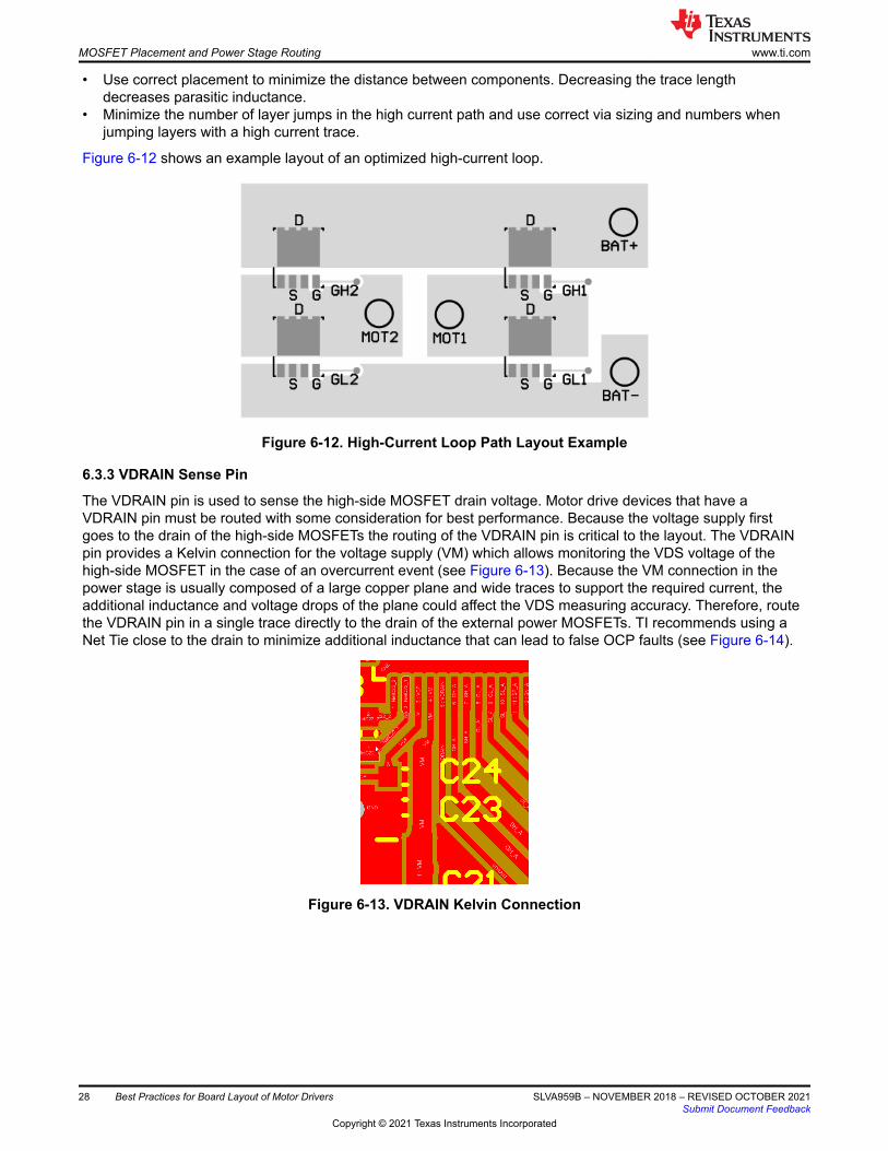
Figure 6-12 shows an example layout of an optimized high-current loop.
Figure 6-12. High-Current Loop Path Layout Example
6.3.3 VDRAIN Sense Pin
The VDRAIN pin is used to sense the high-side MOSFET drain voltage. Motor drive devices that have a VDRAIN pin must be routed with some consideration for best performance. Because the voltage supply first goes to the drain of the high-side MOSFETs the routing of the VDRAIN pin is critical to the layout. The VDRAIN pin provides a Kelvin connection for the voltage supply (VM) which allows monitoring the VDS voltage of the high-side MOSFET in the case of an overcurrent event (see Figure 6-13). Because the VM connection in the power stage is usually composed of a large copper plane and wide traces to support the required current, the additional inductance and voltage drops of the plane could affect the VDS measuring accuracy. Therefore, route the VDRAIN pin in a single trace directly to the drain of the external power MOSFETs. TI recommends using a Net Tie close to the drain to minimize additional inductance that can lead to false OCP faults (see Figure 6-14).
Figure 6-13. VDRAIN Kelvin Connection
MOSFET Placement and Power Stage Routing www.ti.com
28 Best Practices for Board Layout of Motor Drivers SLVA959B – NOVEMBER 2018 – REVISED OCTOBER 2021Submit Document Feedback
Copyright © 2021 Texas Instruments Incorporated
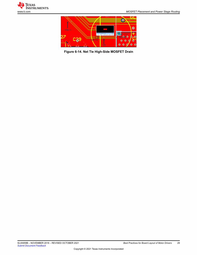
Figure 6-14. Net Tie High-Side MOSFET Drain
www.ti.com MOSFET Placement and Power Stage Routing
SLVA959B – NOVEMBER 2018 – REVISED OCTOBER 2021Submit Document Feedback
Best Practices for Board Layout of Motor Drivers 29
Copyright © 2021 Texas Instruments Incorporated
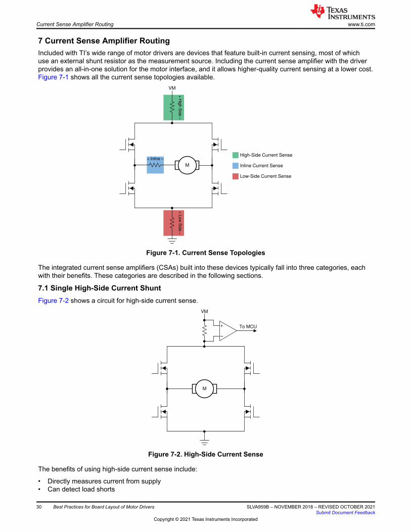
7 Current Sense Amplifier RoutingIncluded with TI’s wide range of motor drivers are devices that feature built-in current sensing, most of which use an external shunt resistor as the measurement source. Including the current sense amplifier with the driver provides an all-in-one solution for the motor interface, and it allows higher-quality current sensing at a lower cost. Figure 7-1 shows all the current sense topologies available.
+ H
igh
Sid
e ±
VM
M
High-Side Current Sense
+ L
ow
Sid
e ±
+ Inline ±
Inline Current Sense
Low-Side Current Sense
Figure 7-1. Current Sense Topologies
The integrated current sense amplifiers (CSAs) built into these devices typically fall into three categories, each with their benefits. These categories are described in the following sections.
7.1 Single High-Side Current ShuntFigure 7-2 shows a circuit for high-side current sense.
VM
M
+
±
To MCU
Figure 7-2. High-Side Current Sense
The benefits of using high-side current sense include:
• Directly measures current from supply• Can detect load shorts
Current Sense Amplifier Routing www.ti.com
30 Best Practices for Board Layout of Motor Drivers SLVA959B – NOVEMBER 2018 – REVISED OCTOBER 2021Submit Document Feedback
Copyright © 2021 Texas Instruments Incorporated
• Immune to ground disturbance
A tradeoff of using high-side current sense is that it requires more common-mode voltage.
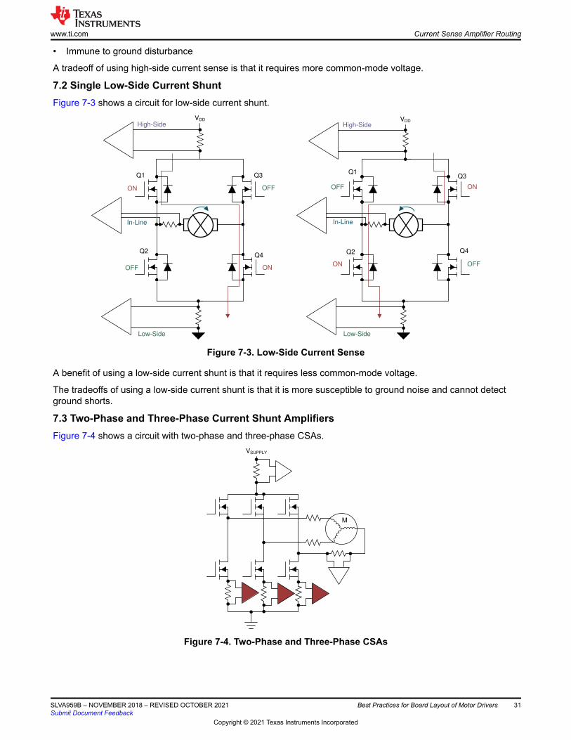
7.2 Single Low-Side Current ShuntFigure 7-3 shows a circuit for low-side current shunt.
OFF
OFF
ON
ON
VDD
Q1
Q2
High-Side
Low-Side
Q4
Q3
OFF
OFF
ON
ON
VDD
Q1
Q2
Low-Side
Q4
Q3
In-Line In-Line
High-Side
Figure 7-3. Low-Side Current Sense
A benefit of using a low-side current shunt is that it requires less common-mode voltage.
The tradeoffs of using a low-side current shunt is that it is more susceptible to ground noise and cannot detect ground shorts.
7.3 Two-Phase and Three-Phase Current Shunt AmplifiersFigure 7-4 shows a circuit with two-phase and three-phase CSAs.
VSUPPLY
M
Figure 7-4. Two-Phase and Three-Phase CSAs
www.ti.com Current Sense Amplifier Routing
SLVA959B – NOVEMBER 2018 – REVISED OCTOBER 2021Submit Document Feedback
Best Practices for Board Layout of Motor Drivers 31
Copyright © 2021 Texas Instruments Incorporated
Two-phase and three-phase CSAs are a benefit to board layout because they have low common-mode voltage requirements. They also let each channel be measured individually, and therefore can be used in more complex control schemes such as field-oriented control.
The tradeoffs of using two-phase and three-phase CSAs in board layout include:• Higher susceptibility to ground noise• Cannot detect ground shorts• Could require more software to realize the total system current
7.4 Component SelectionWhen selecting the sense resistor, there are fundamental tradeoffs between accuracy and power consumption. Because the large currents in the power stage flow through the sense resistor, the selected resistor value must be small to keep the power dissipation at a minimum. For high current systems, the resistor value is usually in mΩ. For example, a system that drives 20 A of current and uses a 1-mΩ sense resistor will dissipates 400 mW from that resistor. Under this condition, the input of the CSA only receives 20 mV of signal. Increasing the resistor value can improve the signal-to-noise ratio but will also increase the power dissipation.
The performance parameters of the CSA must also be considered. When designing for the worst-case current in the system, the selected shunt resistor should prevent voltages on the current sense input pins that are higher than the absolute maximum ratings of the CSA. During normal operation, this voltage must stay within the specified parameters for the differential voltage range. To select the sense resistor, refer to the device data sheet.
For devices that use external gain resistors, such as the DRV3201-Q1, select components that have high accuracy. Component mismatch causes large variations in both the common mode and differential mode gains across systems.
7.5 PlacementPlacement of the sense resistor should be in line with the components of the power stage to minimize trace impedance. The shunt resistor should also be placed close to the connection to the CSA to decrease the possibility of coupling on other traces on the board.
For high-side current sense, the shunt resistor should be near the star point between the supply and the source of the high-side MOSFETs. For high-side current sense devices that use external gain resistors, such as the DRV3205-Q1, the first resistor in the divider should be placed nearest to the shunt resistor. The remaining components should be placed nearest to the device.
For low-side current sense, the shunt resistor should be between the source of the low-side MOSFET and the star point ground connection of the power stage.
For systems with shunt resistors on two or three individual phases, the shunt resistor should be placed between the source of the respective low-side MOSFET and the star point ground connection.
7.6 RoutingRouting of the sense signals must be done using a differential pair. In a differential pair, both signals are tightly coupled in the layout and the traces must run parallel from the shunt or sense resistor to the CSA at the input of the IC.
Current Sense Amplifier Routing www.ti.com
32 Best Practices for Board Layout of Motor Drivers SLVA959B – NOVEMBER 2018 – REVISED OCTOBER 2021Submit Document Feedback
Copyright © 2021 Texas Instruments Incorporated
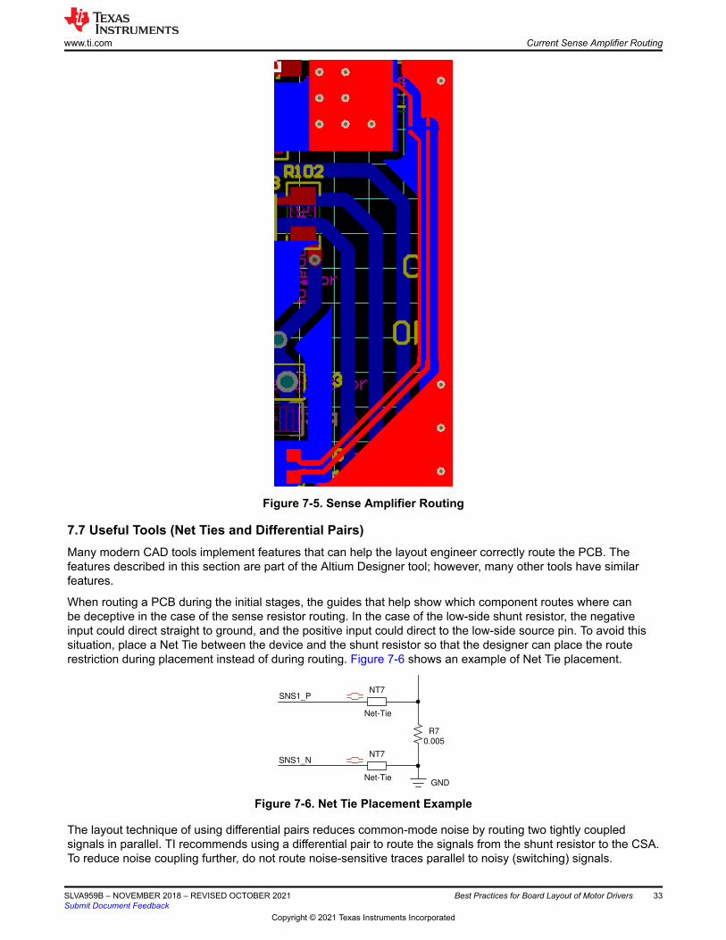
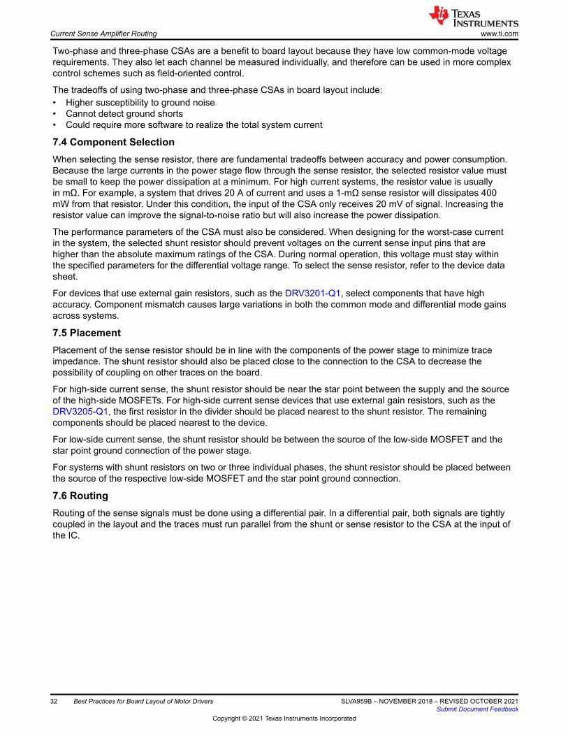
Figure 7-5. Sense Amplifier Routing
7.7 Useful Tools (Net Ties and Differential Pairs)Many modern CAD tools implement features that can help the layout engineer correctly route the PCB. The features described in this section are part of the Altium Designer tool; however, many other tools have similar features.
When routing a PCB during the initial stages, the guides that help show which component routes where can be deceptive in the case of the sense resistor routing. In the case of the low-side shunt resistor, the negative input could direct straight to ground, and the positive input could direct to the low-side source pin. To avoid this situation, place a Net Tie between the device and the shunt resistor so that the designer can place the route restriction during placement instead of during routing. Figure 7-6 shows an example of Net Tie placement.
R7
0.005
NT7
NT7
GND
Net-Tie
Net-Tie
SNS1_P
SNS1_N
Figure 7-6. Net Tie Placement Example
The layout technique of using differential pairs reduces common-mode noise by routing two tightly coupled signals in parallel. TI recommends using a differential pair to route the signals from the shunt resistor to the CSA. To reduce noise coupling further, do not route noise-sensitive traces parallel to noisy (switching) signals.
www.ti.com Current Sense Amplifier Routing
SLVA959B – NOVEMBER 2018 – REVISED OCTOBER 2021Submit Document Feedback
Best Practices for Board Layout of Motor Drivers 33
Copyright © 2021 Texas Instruments Incorporated
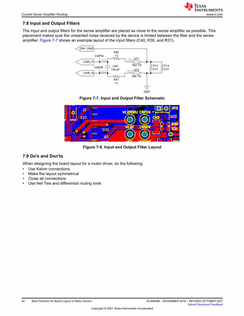
7.8 Input and Output FiltersThe input and output filters for the sense amplifier are placed as close to the sense amplifier as possible. This placement makes sure the unwanted noise received by the device is limited between the filter and the sense amplifier. Figure 7-7 shows an example layout of the input filters (C40, R30, and R31).
R14
0.01
R13
0.01
GND
NT2
Net-Tie
NT1
Net-Tie
R30
1 k
R311 k
C40
100 pFCSNIN
CSPIN
DRV_GND
CSIN_P
CSIN_N
Figure 7-7. Input and Output Filter Schematic
Figure 7-8. Input and Output Filter Layout
7.9 Do's and Don'tsWhen designing the board layout for a motor driver, do the following:• Use Kelvin connections• Make the layout symmetrical• Close all connections• Use Net Ties and differential routing tools
Current Sense Amplifier Routing www.ti.com
34 Best Practices for Board Layout of Motor Drivers SLVA959B – NOVEMBER 2018 – REVISED OCTOBER 2021Submit Document Feedback
Copyright © 2021 Texas Instruments Incorporated
8 ReferencesFor additional reference, refer to the following:
• Texas Instruments, AN-1520 A Guide to Board Layout for Best Thermal Resistance for Exposed Packages application report
• Texas Instruments, AN-2020 Thermal Design By Insight, Not Hindsight application report• Texas Instruments, Analog-to-Digital Converter Grounding Practices Affect System Performance application
report• Texas Instruments, Grounding in mixed-signal systems demystified, Part 1 technical brief• Texas Instruments, Grounding in mixed-signal systems demystified, Part 2• Texas Instruments, PCB Design Guidelines For Reduced EMI application report• Texas Instruments, PowerPAD™ Thermally Enhanced Package application report• Texas Instruments, Printed-Circuit-Board Layout for Improved Electromagnetic Compatibility application
report• Texas Instruments, Thermal Characteristics of Linear and Logic Packages Using JEDEC PCB Designs
application report
9 Revision HistoryChanges from Revision A (January 2019) to Revision B (October 2021) Page• Updated the numbering format for tables, figures, and cross-references throughout the document..................1
www.ti.com References
SLVA959B – NOVEMBER 2018 – REVISED OCTOBER 2021Submit Document Feedback
Best Practices for Board Layout of Motor Drivers 35
Copyright © 2021 Texas Instruments Incorporated

IMPORTANT NOTICE AND DISCLAIMERTI PROVIDES TECHNICAL AND RELIABILITY DATA (INCLUDING DATA SHEETS), DESIGN RESOURCES (INCLUDING REFERENCE DESIGNS), APPLICATION OR OTHER DESIGN ADVICE, WEB TOOLS, SAFETY INFORMATION, AND OTHER RESOURCES “AS IS” AND WITH ALL FAULTS, AND DISCLAIMS ALL WARRANTIES, EXPRESS AND IMPLIED, INCLUDING WITHOUT LIMITATION ANY IMPLIED WARRANTIES OF MERCHANTABILITY, FITNESS FOR A PARTICULAR PURPOSE OR NON-INFRINGEMENT OF THIRD PARTY INTELLECTUAL PROPERTY RIGHTS.These resources are intended for skilled developers designing with TI products. You are solely responsible for (1) selecting the appropriate TI products for your application, (2) designing, validating and testing your application, and (3) ensuring your application meets applicable standards, and any other safety, security, regulatory or other requirements.These resources are subject to change without notice. TI grants you permission to use these resources only for development of an application that uses the TI products described in the resource. Other reproduction and display of these resources is prohibited. No license is granted to any other TI intellectual property right or to any third party intellectual property right. TI disclaims responsibility for, and you will fully indemnify TI and its representatives against, any claims, damages, costs, losses, and liabilities arising out of your use of these resources.TI’s products are provided subject to TI’s Terms of Sale or other applicable terms available either on ti.com or provided in conjunction with such TI products. TI’s provision of these resources does not expand or otherwise alter TI’s applicable warranties or warranty disclaimers for TI products.TI objects to and rejects any additional or different terms you may have proposed. IMPORTANT NOTICE
Mailing Address: Texas Instruments, Post Office Box 655303, Dallas, Texas 75265Copyright © 2021, Texas Instruments Incorporated