Embed Size (px)
Citation preview

Production Datasheet
LX7720
June 2020 LX7720 rev 1.1 1 © 2020 Microsemi Corporation
Motor Driver with Four Half-Bridge Drivers, Rotation and Position Sensing for Space Description The LX7720 is a spacecraft motor driver that is radiation-hardened by design and works with either a space FPGA controller such as RTG4, RTAX-S/SL, and RT PolarFire, or a space MCU such as SAMRH71F20, SAMV71Q21RT, and SAM3X8ERT. The LX7720 contains four half-bridge drivers with floating current sense for motor coil driving, six bi-level inputs for sensing Hall effect sensors or rotary encoders, and a resolver or LVDT interface to digital with primary coil driver. The LX7720 works with an FPGA or MCU system controller to provide a complete closed loop motor driver with coil current feedback and rotation or linear position sensing. With flexible programming, the combined system can provide motor control for stepper motors, brushless DC and permanent magnet motors. Position sensing supports encoders, Hall effect sensors, resolvers, synchros, and LVDTs. FPGA and MCU IP modules are available to support motor driving functions from open loop cardinal step driving to space vector modulation using field-oriented control. The LX7720 contains 7 sigma delta modulators for analog sampling. Sinc3 filtering and decimation is performed in the FPGA or microcontroller with available IP modules. Four of the modulators sample the voltage across floating current sense inputs and three modulators sample differential analog inputs such as the outputs of a resolver transformer. Speed versus accuracy tradeoffs can be exploited. The LX7720 supports a ground potential difference between the motor and signal grounds in the range of -10V to +8V and motor supply voltages up to 60V. Resolver or LVDT carrier frequencies from 360Hz to 20kHz are supported. The LX7720MFQ is packaged in a 132 pin hermetic ceramic quad flat pack. The LX7720MMF is packaged in a lead-free 208 pin non-hermetic plastic quad flat pack. Both parts operate over a -55°C to 125°C temperature range, and are radiation tolerant to 100krad(Si) TID and 50krad(Si) ELDRs, as well as single event effects.
Features • Four half-bridge N-channel MOSFET drivers • Four floating differential current sensors • Pulse modulated resolver/LVDT transformer driver • Three differential resolver/LVDT sense inputs • Six threshold adjustable bi-level logic inputs for Hall
effect sensor/encoder interfaces • Fault detection • Radiation tolerant: 100krad(Si) TID, 50krad(Si)
ELDRS, SEL immune up to 60MeV.cm²/mg and 125°C (fluence of 107 particles/cm²)
Applications • Motor driver servo control • Linear actuator servo control • Stepper, BLDC, PMSM motor driver • Robotics
Typical Motor Drive System
Radiation Tolerant Power Driver with Four Half-Bridge Drivers, Rotation and Position Sensing
June 2020 LX7720 rev 1.1 2 © 2020 Microsemi Corporation
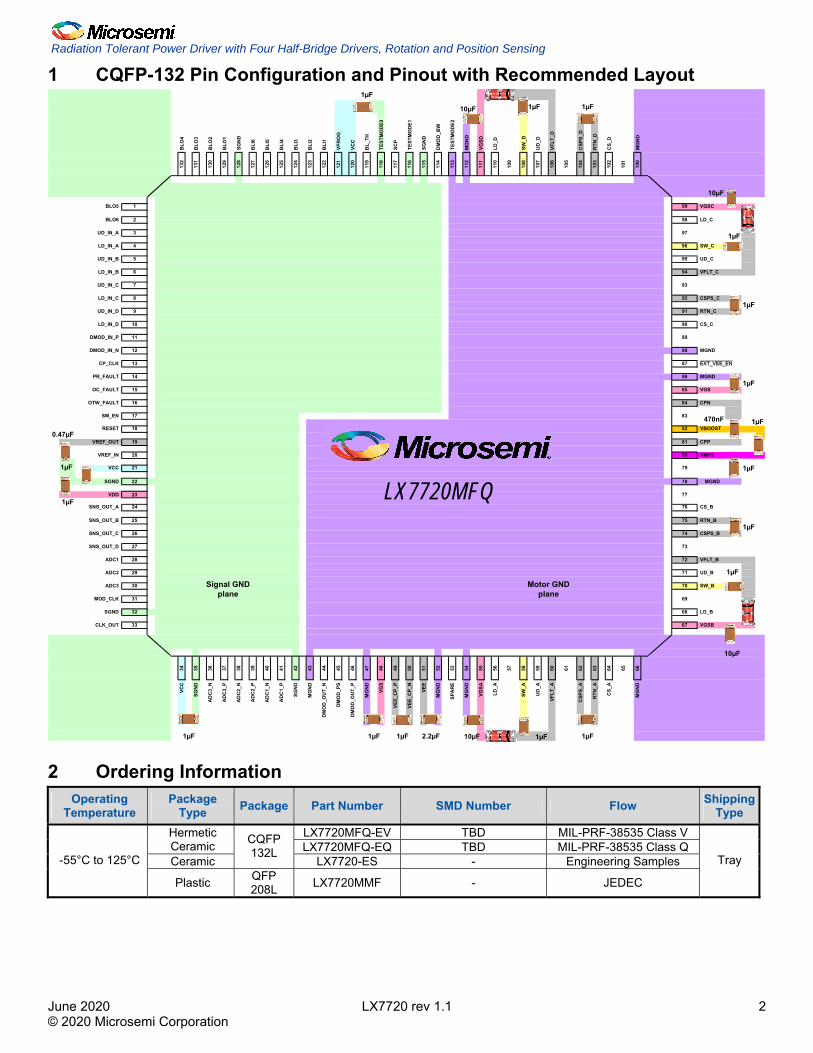
1 CQFP-132 Pin Configuration and Pinout with Recommended Layout
BLO
4
BLO
3
BLO
2
BLO
1
SGN
D
BLI
6
BLI
5
BLI
4
BLI
3
BLI
2
BLI
1
VPR
OG
VCC
BL_
TH
TEST
MO
DE0
SCP
TEST
MO
DE1
SGN
D
DM
OD
_BW
TEST
MO
DE2
MG
ND
VGSD
LD_D
SW_D
UD
_D
VFLT
_D
CSP
S_D
RTN
_D
CS_
D
MG
ND
132
131
130
129
128
127
126
125
124
123
122
121
120
119
118
117
116
115
114
113
112
111
110
109
108
107
106
105
104
103
102
101
100
10µF
BLO5 1 99 VGSC
BLO6 2 98 LD_C
UD_IN_A 3 97
LD_IN_A 4 96 SW_C
UD_IN_B 5 95 UD_C
LD_IN_B 6 94 VFLT_C
UD_IN_C 7 93
LD_IN_C 8 92 CSPS_C
UD_IN_D 9 91 RTN_C
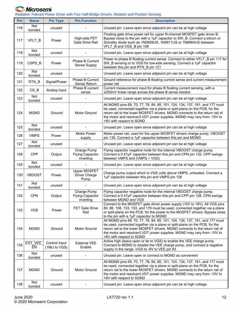
LD_IN_D 10 90 CS_C
DMOD_IN_P 11 89
DMOD_IN_N 12 88 MGND
CP_CLK 13 87 EXT_VEE_EN
PR_FAULT 14 86 MGND
OC_FAULT 15 85 VGS
OTW_FAULT 16 84 CPN
SM_EN 17 83
RESET 18 82 VBOOST
VREF_OUT 19 81 CPP
VREF_IN 20 80 VMPS
VCC 21 79
SGND 22 78 MGND
VDD 23 77
SNS_OUT_A 24 76 CS_B
SNS_OUT_B 25 75 RTN_B
SNS_OUT_C 26 74 CSPS_B
SNS_OUT_D 27 73
ADC1 28 72 VFLT_B
ADC2 29 71 UD_B
ADC3 30 70 SW_B
MOD_CLK 31 69
SGND 32 68 LD_B
CLK_OUT 33 67 VGSB
34 35 36 37 38 39 40 41 42 43 44 45 46 47 48 49 50 51 52 53 54 55 56 57 58 59 60 61 62 63 64 65 66
VCC
SGN
D
AD
C3_
N
AD
C3_
P
AD
C2_
N
AD
C2_
P
AD
C1_
N
AD
C1_
P
SGN
D
MG
ND
DM
OD
_OU
T_N
DM
OD
_PS
DM
OD
_OU
T_P
MG
ND
VGS
VEE_
CP_
P
VEE_
CP_
N
VEE
MG
ND
SPA
RE
MG
ND
VGSA
LD_A
SW_A
UD
_A
VFLT
_A
CSP
S_A
RTN
_A
CS_
A
MG
ND
10µF 1µF
1µF
1µF
1µF
10µF 1µF
10µF
1µF
1µF
1µF
1µF
1µF
1µF470nF
1µF
1µF 1µF 1µF 2.2µF
LX7720MFQ
Signal GNDplane
Motor GNDplane
0.47µF
1µF
1µF
2 Ordering Information Operating
Temperature Package
Type Package Part Number SMD Number Flow Shipping Type
LX7720MFQ-EV TBD MIL-PRF-38535 Class V Hermetic Ceramic LX7720MFQ-EQ TBD MIL-PRF-38535 Class Q Ceramic
CQFP 132L
LX7720-ES - Engineering Samples -55°C to 125°C
Plastic QFP 208L LX7720MMF - JEDEC
Tray
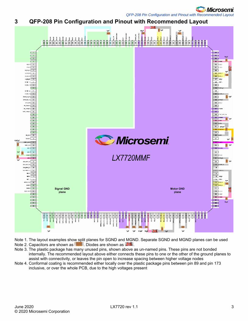
QFP-208 Pin Configuration and Pinout with Recommended Layout
June 2020 LX7720 rev 1.1 3 © 2020 Microsemi Corporation
3 QFP-208 Pin Configuration and Pinout with Recommended Layout
Note 1. The layout examples show split planes for SGND and MGND. Separate SGND and MGND planes can be used Note 2. Capacitors are shown as . Diodes are shown as . Note 3. The plastic package has many unused pins, shown above as un-named pins. These pins are not bonded
internally. The recommended layout above either connects these pins to one or the other of the ground planes to assist with connectivity, or leaves the pin open to increase spacing between higher voltage nodes
Note 4. Conformal coating is recommended either locally over the plastic package pins between pin 89 and pin 173 inclusive, or over the whole PCB, due to the high voltages present
Radiation Tolerant Power Driver with Four Half-Bridge Drivers, Rotation and Position Sensing
June 2020 LX7720 rev 1.1 4 © 2020 Microsemi Corporation
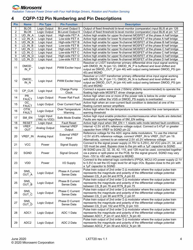
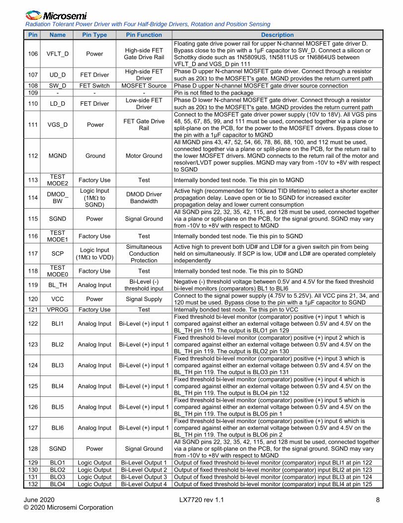
4 CQFP-132 Pin Numbering and Pin Descriptions Pin Name Pin Type Pin Function Description 1 BLO5 Logic Output Bi-Level Output 5 Output of fixed threshold bi-level monitor (comparator) input BLI5 at pin 126 2 BLO6 Logic Output Bi-Level Output 6 Output of fixed threshold bi-level monitor (comparator) input BLI6 at pin 127 3 UD_IN_A Logic Input High-side FET A Active high enable for upper N-channel MOSFET of the phase A half bridge 4 LD_IN_A Logic Input Low-side FET A Active high enable for lower N-channel MOSFET of the phase A half bridge 5 UD_IN_B Logic Input High-side FET B Active high enable for upper N-channel MOSFET of the phase B half bridge 6 LD_IN_B Logic Input Low-side FET B Active high enable for lower N-channel MOSFET of the phase B half bridge 7 UD_IN_C Logic Input High-side FET C Active high enable for upper N-channel MOSFET of the phase C half bridge 8 LD_IN_C Logic Input Low-side FET C Active high enable for lower N-channel MOSFET of the phase C half bridge 9 UD_IN_D Logic Input High-side FET D Active high enable for upper N-channel MOSFET of the phase D half bridge 10 LD_IN_D Logic Input Low-side FET D Active high enable for lower N-channel MOSFET of the phase D half bridge
11 DMOD_ IN_P Logic Input PWM Exciter Input
Resolver or LVDT transformer primary differential drive input signal working with DMOD_IN_N (pin 12). DMOD_IN_P is buffered and level shifted and output as DMOD_OUT_P (pin 46) with output swing between DMOD_PS (pin 45) and MGND
12 DMOD_ IN_N Logic Input PWM Exciter Input
Resolver or LVDT transformer primary differential drive input signal working with DMOD_IN_P (pin 11). DMOD_IN_N is buffered and level shifted and output as DMOD_OUT_N (pin 44) with output swing between DMOD_PS (pin 45) and MGND
13 CP_CLK Logic Input Charge Pump Clock
Connect a square wave clock (150kHz ±50kHz recommended) to operate the floating high-side MOSFET driver charge pump
14 PR_ FAULT Logic Output Power Rail Fault Active high when one or more of the power rails is below its under voltage
threshold or either the VGS or DMOD_PS supply is overloaded
15 OC_ FAULT Logic Output Over Current Fault Active high when an over-current fault condition is detected at one of the
floating current sensor amplifiers
16 OTW_ FAULT Logic Output Over Temperature
Warning Active high when the die temperature is has exceeded the over temperature warning threshold
17 SM_EN Logic Input (1MΩ to VDD) Safe Mode Enable Active high input enable protection countermeasures when faults are detected.
Faults are reported regardless of SM_EN setting 18 RESET Logic Input Fault Reset Active high input when SM_EN = 1 resets safe mode latched fault conditions
19 VREF_ OUT Analog Output Internal VREF
Output Internal +2.5V ±0.8% reference voltage output. Connect a 0.47µF or greater capacitor from VREF to SGND pin 22
20 VREF_IN Analog Input External VREF Input
Reference voltage for the ADC sigma delta modulators. To use the internal +2.5V ±0.8% reference voltage, connect VREF_IN to VREF_OUT pin 19. Alternatively, connect to an external 2.5V ±0.2V reference voltage
21 VCC Power Signal Supply Connect to the signal power supply (4.75V to 5.25V). All VCC pins 21, 34, and 120 must be used. Bypass close to the pin with a 1µF capacitor to SGND
22 SGND Power Signal Ground All SGND pins 22, 32, 35, 42, 115, and 128 must be used, connected together via a plane or split-plane on the PCB, for the signal ground. SGND may vary from -10V to +8V with respect to MGND
23 VDD Power I/O Supply Connect to the external logic controller's (FPGA, MCU) I/O power supply (2.1V to 5.5V) to set the I/O logic level for all logic I/Os. Bypass close to the pin with a 1µF capacitor to SGND
24 SNS_ OUT_A Logic Output Phase A Current
Sense Data
Pulse train output of 2nd order Σ-Δ modulator where the output pulse train represents the magnitude and polarity of the differential voltage potential between CS_A pin 64 and RTN_A pin 63
25 SNS_ OUT_B Logic Output Phase B Current
Sense Data
Pulse train output of 2nd order Σ-Δ modulator where the output pulse train represents the magnitude and polarity of the differential voltage potential between CS_B pin 76 and RTN_B pin 75
26 SNS_ OUT_C Logic Output Phase C Current
Sense Data
Pulse train output of 2nd order Σ-Δ modulator where the output pulse train represents the magnitude and polarity of the differential voltage potential between CS_C pin 90 and RTN_C pin 91
27 SNS_ OUT_D Logic Output Phase D Current
Sense Data
Pulse train output of 2nd order Σ-Δ modulator where the output pulse train represents the magnitude and polarity of the differential voltage potential between CS_D pin 102 and RTN_D pin 103
28 ADC1 Logic Output ADC 1 Data Pulse train output of 2nd order Σ-Δ modulator where the output pulse train represents the magnitude and polarity of the differential voltage potential between ADC1_P pin 41 and ADC1_N pin 40
29 ADC2 Logic Output ADC 2 Data Pulse train output of 2nd order Σ-Δ modulator where the output pulse train represents the magnitude and polarity of the differential voltage potential between ADC2_P pin 39 and ADC2_N pin 38
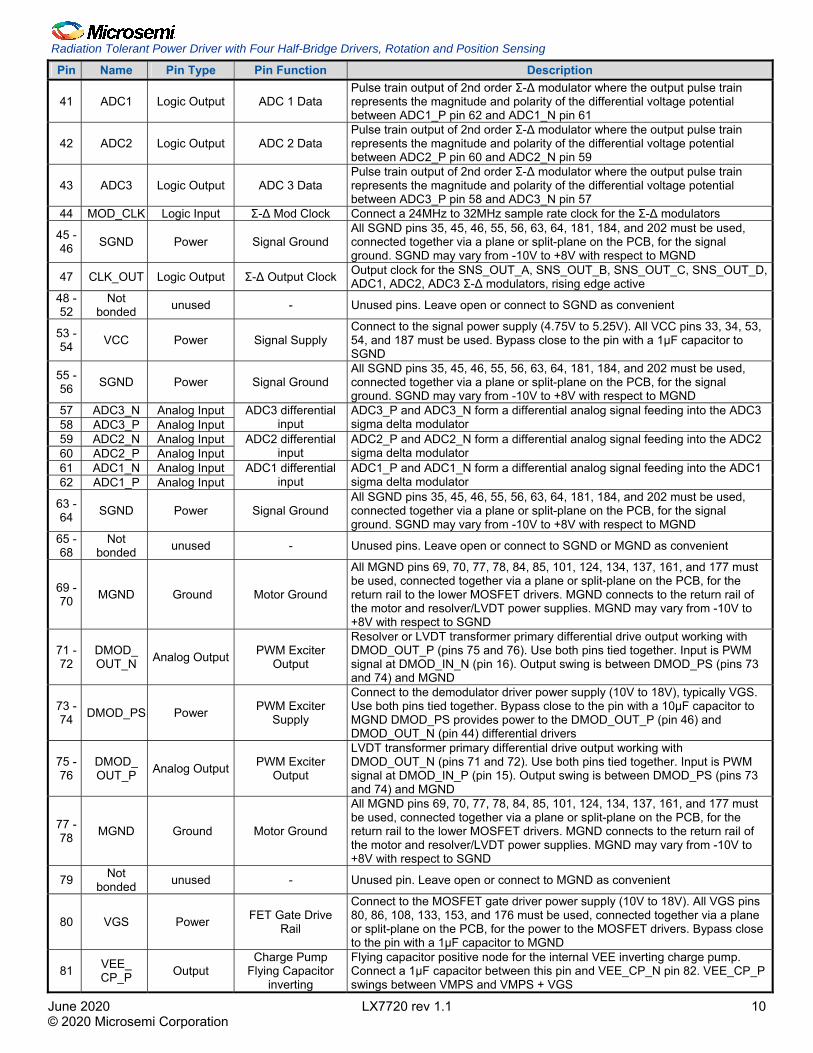
CQFP-132 Pin Numbering and Pin Descriptions
June 2020 LX7720 rev 1.1 5 © 2020 Microsemi Corporation
Pin Name Pin Type Pin Function Description
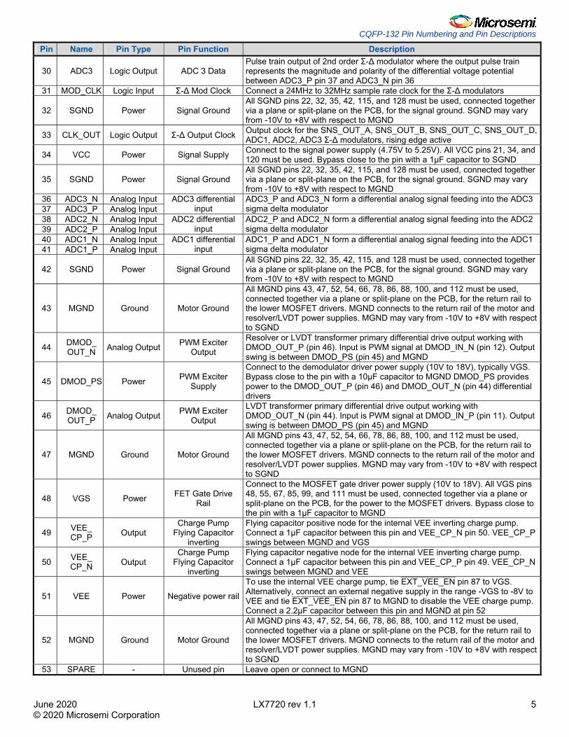
30 ADC3 Logic Output ADC 3 Data Pulse train output of 2nd order Σ-Δ modulator where the output pulse train represents the magnitude and polarity of the differential voltage potential between ADC3_P pin 37 and ADC3_N pin 36
31 MOD_CLK Logic Input Σ-Δ Mod Clock Connect a 24MHz to 32MHz sample rate clock for the Σ-Δ modulators
32 SGND Power Signal Ground All SGND pins 22, 32, 35, 42, 115, and 128 must be used, connected together via a plane or split-plane on the PCB, for the signal ground. SGND may vary from -10V to +8V with respect to MGND
33 CLK_OUT Logic Output Σ-Δ Output Clock Output clock for the SNS_OUT_A, SNS_OUT_B, SNS_OUT_C, SNS_OUT_D, ADC1, ADC2, ADC3 Σ-Δ modulators, rising edge active
34 VCC Power Signal Supply Connect to the signal power supply (4.75V to 5.25V). All VCC pins 21, 34, and 120 must be used. Bypass close to the pin with a 1µF capacitor to SGND
35 SGND Power Signal Ground All SGND pins 22, 32, 35, 42, 115, and 128 must be used, connected together via a plane or split-plane on the PCB, for the signal ground. SGND may vary from -10V to +8V with respect to MGND
36 ADC3_N Analog Input 37 ADC3_P Analog Input
ADC3 differential input
ADC3_P and ADC3_N form a differential analog signal feeding into the ADC3 sigma delta modulator
38 ADC2_N Analog Input 39 ADC2_P Analog Input
ADC2 differential input
ADC2_P and ADC2_N form a differential analog signal feeding into the ADC2 sigma delta modulator
40 ADC1_N Analog Input 41 ADC1_P Analog Input
ADC1 differential input
ADC1_P and ADC1_N form a differential analog signal feeding into the ADC1 sigma delta modulator
42 SGND Power Signal Ground All SGND pins 22, 32, 35, 42, 115, and 128 must be used, connected together via a plane or split-plane on the PCB, for the signal ground. SGND may vary from -10V to +8V with respect to MGND
43 MGND Ground Motor Ground
All MGND pins 43, 47, 52, 54, 66, 78, 86, 88, 100, and 112 must be used, connected together via a plane or split-plane on the PCB, for the return rail to the lower MOSFET drivers. MGND connects to the return rail of the motor and resolver/LVDT power supplies. MGND may vary from -10V to +8V with respect to SGND
44 DMOD_ OUT_N Analog Output PWM Exciter
Output
Resolver or LVDT transformer primary differential drive output working with DMOD_OUT_P (pin 46). Input is PWM signal at DMOD_IN_N (pin 12). Output swing is between DMOD_PS (pin 45) and MGND
45 DMOD_PS Power PWM Exciter Supply
Connect to the demodulator driver power supply (10V to 18V), typically VGS. Bypass close to the pin with a 10µF capacitor to MGND DMOD_PS provides power to the DMOD_OUT_P (pin 46) and DMOD_OUT_N (pin 44) differential drivers
46 DMOD_ OUT_P Analog Output PWM Exciter
Output
LVDT transformer primary differential drive output working with DMOD_OUT_N (pin 44). Input is PWM signal at DMOD_IN_P (pin 11). Output swing is between DMOD_PS (pin 45) and MGND
47 MGND Ground Motor Ground
All MGND pins 43, 47, 52, 54, 66, 78, 86, 88, 100, and 112 must be used, connected together via a plane or split-plane on the PCB, for the return rail to the lower MOSFET drivers. MGND connects to the return rail of the motor and resolver/LVDT power supplies. MGND may vary from -10V to +8V with respect to SGND
48 VGS Power FET Gate Drive Rail
Connect to the MOSFET gate driver power supply (10V to 18V). All VGS pins 48, 55, 67, 85, 99, and 111 must be used, connected together via a plane or split-plane on the PCB, for the power to the MOSFET drivers. Bypass close to the pin with a 1µF capacitor to MGND
49 VEE_ CP_P Output
Charge Pump Flying Capacitor
inverting
Flying capacitor positive node for the internal VEE inverting charge pump. Connect a 1µF capacitor between this pin and VEE_CP_N pin 50. VEE_CP_P swings between MGND and VGS
50 VEE_ CP_N Output
Charge Pump Flying Capacitor
inverting
Flying capacitor negative node for the internal VEE inverting charge pump. Connect a 1µF capacitor between this pin and VEE_CP_P pin 49. VEE_CP_N swings between MGND and VEE
51 VEE Power Negative power rail
To use the internal VEE charge pump, tie EXT_VEE_EN pin 87 to VGS. Alternatively, connect an external negative supply in the range -VGS to -8V to VEE and tie EXT_VEE_EN pin 87 to MGND to disable the VEE charge pump. Connect a 2.2µF capacitor between this pin and MGND at pin 52
52 MGND Ground Motor Ground
All MGND pins 43, 47, 52, 54, 66, 78, 86, 88, 100, and 112 must be used, connected together via a plane or split-plane on the PCB, for the return rail to the lower MOSFET drivers. MGND connects to the return rail of the motor and resolver/LVDT power supplies. MGND may vary from -10V to +8V with respect to SGND
53 SPARE - Unused pin Leave open or connect to MGND
Radiation Tolerant Power Driver with Four Half-Bridge Drivers, Rotation and Position Sensing
June 2020 LX7720 rev 1.1 6 © 2020 Microsemi Corporation
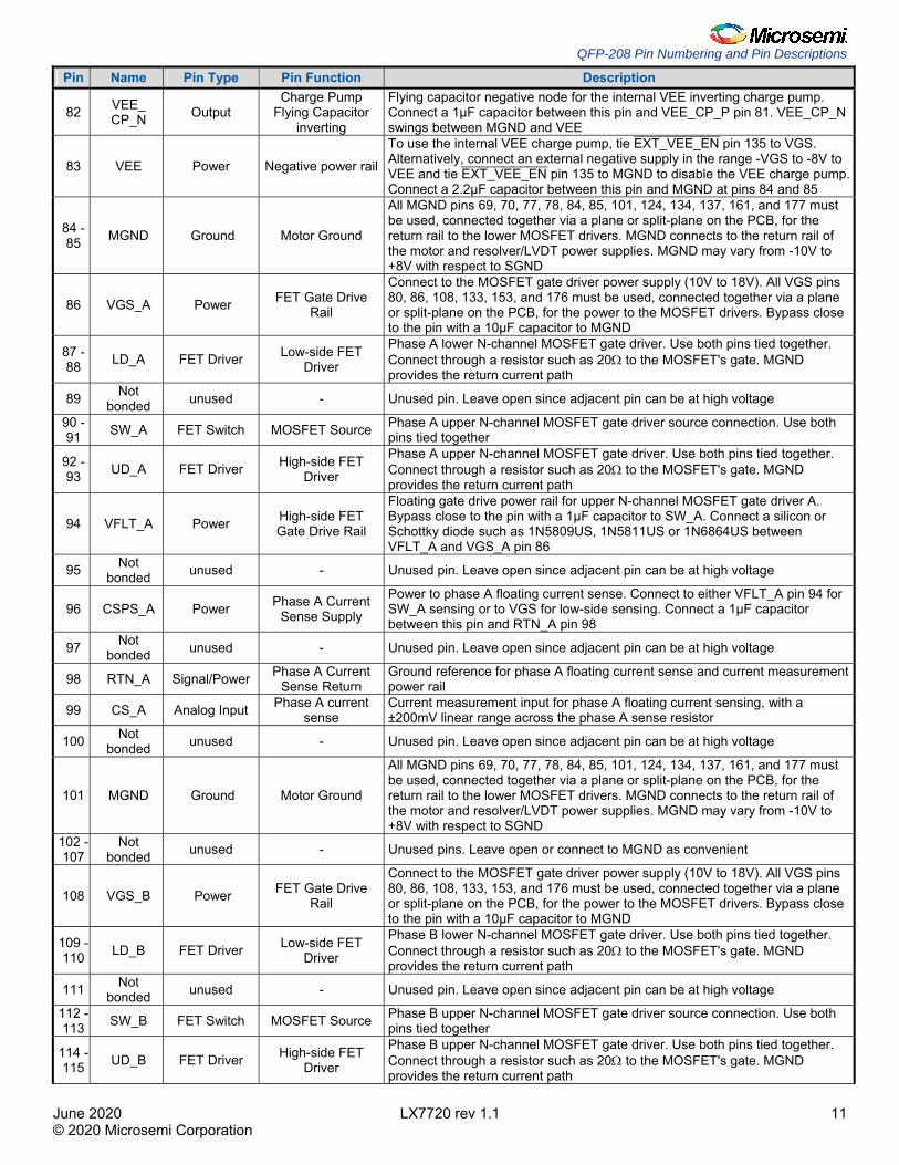
Pin Name Pin Type Pin Function Description
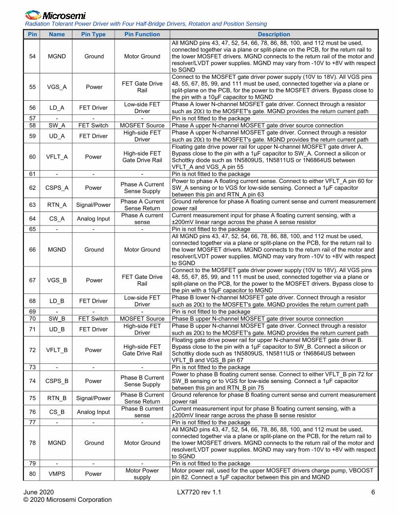
54 MGND Ground Motor Ground
All MGND pins 43, 47, 52, 54, 66, 78, 86, 88, 100, and 112 must be used, connected together via a plane or split-plane on the PCB, for the return rail to the lower MOSFET drivers. MGND connects to the return rail of the motor and resolver/LVDT power supplies. MGND may vary from -10V to +8V with respect to SGND
55 VGS_A Power FET Gate Drive Rail
Connect to the MOSFET gate driver power supply (10V to 18V). All VGS pins 48, 55, 67, 85, 99, and 111 must be used, connected together via a plane or split-plane on the PCB, for the power to the MOSFET drivers. Bypass close to the pin with a 10µF capacitor to MGND
56 LD_A FET Driver Low-side FET Driver
Phase A lower N-channel MOSFET gate driver. Connect through a resistor such as 20Ω to the MOSFET's gate. MGND provides the return current path
57 - - - Pin is not fitted to the package 58 SW_A FET Switch MOSFET Source Phase A upper N-channel MOSFET gate driver source connection
59 UD_A FET Driver High-side FET Driver
Phase A upper N-channel MOSFET gate driver. Connect through a resistor such as 20Ω to the MOSFET's gate. MGND provides the return current path
60 VFLT_A Power High-side FET Gate Drive Rail
Floating gate drive power rail for upper N-channel MOSFET gate driver A. Bypass close to the pin with a 1µF capacitor to SW_A. Connect a silicon or Schottky diode such as 1N5809US, 1N5811US or 1N6864US between VFLT_A and VGS_A pin 55
61 - - - Pin is not fitted to the package
62 CSPS_A Power Phase A Current Sense Supply
Power to phase A floating current sense. Connect to either VFLT_A pin 60 for SW_A sensing or to VGS for low-side sensing. Connect a 1µF capacitor between this pin and RTN_A pin 63
63 RTN_A Signal/Power Phase A Current Sense Return
Ground reference for phase A floating current sense and current measurement power rail
64 CS_A Analog Input Phase A current sense
Current measurement input for phase A floating current sensing, with a ±200mV linear range across the phase A sense resistor
65 - - - Pin is not fitted to the package
66 MGND Ground Motor Ground
All MGND pins 43, 47, 52, 54, 66, 78, 86, 88, 100, and 112 must be used, connected together via a plane or split-plane on the PCB, for the return rail to the lower MOSFET drivers. MGND connects to the return rail of the motor and resolver/LVDT power supplies. MGND may vary from -10V to +8V with respect to SGND
67 VGS_B Power FET Gate Drive Rail
Connect to the MOSFET gate driver power supply (10V to 18V). All VGS pins 48, 55, 67, 85, 99, and 111 must be used, connected together via a plane or split-plane on the PCB, for the power to the MOSFET drivers. Bypass close to the pin with a 10µF capacitor to MGND
68 LD_B FET Driver Low-side FET Driver
Phase B lower N-channel MOSFET gate driver. Connect through a resistor such as 20Ω to the MOSFET's gate. MGND provides the return current path
69 - - - Pin is not fitted to the package 70 SW_B FET Switch MOSFET Source Phase B upper N-channel MOSFET gate driver source connection
71 UD_B FET Driver High-side FET Driver
Phase B upper N-channel MOSFET gate driver. Connect through a resistor such as 20Ω to the MOSFET's gate. MGND provides the return current path
72 VFLT_B Power High-side FET Gate Drive Rail
Floating gate drive power rail for upper N-channel MOSFET gate driver B. Bypass close to the pin with a 1µF capacitor to SW_B. Connect a silicon or Schottky diode such as 1N5809US, 1N5811US or 1N6864US between VFLT_B and VGS_B pin 67
73 - - - Pin is not fitted to the package
74 CSPS_B Power Phase B Current Sense Supply
Power to phase B floating current sense. Connect to either VFLT_B pin 72 for SW_B sensing or to VGS for low-side sensing. Connect a 1µF capacitor between this pin and RTN_B pin 75
75 RTN_B Signal/Power Phase B Current Sense Return
Ground reference for phase B floating current sense and current measurement power rail
76 CS_B Analog Input Phase B current sense
Current measurement input for phase B floating current sensing, with a ±200mV linear range across the phase B sense resistor
77 - - - Pin is not fitted to the package
78 MGND Ground Motor Ground
All MGND pins 43, 47, 52, 54, 66, 78, 86, 88, 100, and 112 must be used, connected together via a plane or split-plane on the PCB, for the return rail to the lower MOSFET drivers. MGND connects to the return rail of the motor and resolver/LVDT power supplies. MGND may vary from -10V to +8V with respect to SGND
79 - - - Pin is not fitted to the package
80 VMPS Power Motor Power supply
Motor power rail, used for the upper MOSFET drivers charge pump, VBOOST pin 82. Connect a 1µF capacitor between this pin and MGND
CQFP-132 Pin Numbering and Pin Descriptions
June 2020 LX7720 rev 1.1 7 © 2020 Microsemi Corporation
Pin Name Pin Type Pin Function Description
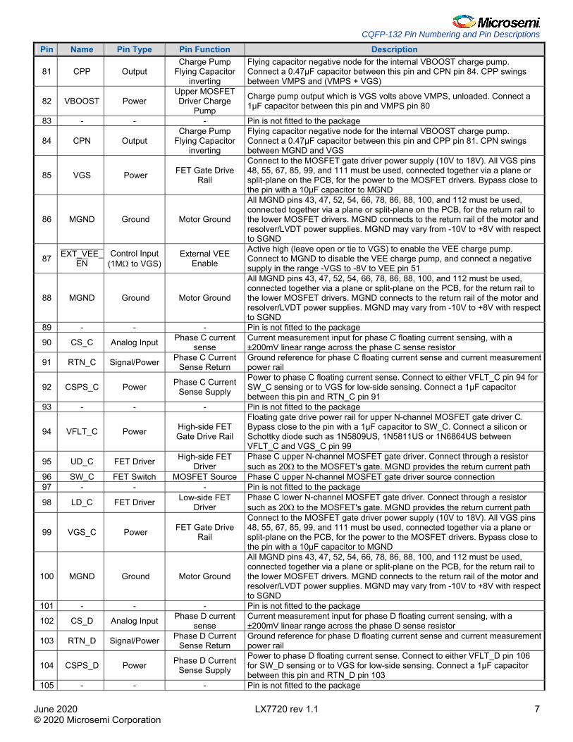
81 CPP Output Charge Pump
Flying Capacitor inverting
Flying capacitor negative node for the internal VBOOST charge pump. Connect a 0.47µF capacitor between this pin and CPN pin 84. CPP swings between VMPS and (VMPS + VGS)
82 VBOOST Power Upper MOSFET Driver Charge
Pump
Charge pump output which is VGS volts above VMPS, unloaded. Connect a 1µF capacitor between this pin and VMPS pin 80
83 - - - Pin is not fitted to the package
84 CPN Output Charge Pump
Flying Capacitor inverting
Flying capacitor negative node for the internal VBOOST charge pump. Connect a 0.47µF capacitor between this pin and CPP pin 81. CPN swings between MGND and VGS
85 VGS Power FET Gate Drive Rail
Connect to the MOSFET gate driver power supply (10V to 18V). All VGS pins 48, 55, 67, 85, 99, and 111 must be used, connected together via a plane or split-plane on the PCB, for the power to the MOSFET drivers. Bypass close to the pin with a 10µF capacitor to MGND
86 MGND Ground Motor Ground
All MGND pins 43, 47, 52, 54, 66, 78, 86, 88, 100, and 112 must be used, connected together via a plane or split-plane on the PCB, for the return rail to the lower MOSFET drivers. MGND connects to the return rail of the motor and resolver/LVDT power supplies. MGND may vary from -10V to +8V with respect to SGND
87 EXT_VEE_EN
Control Input (1MΩ to VGS)
External VEE Enable
Active high (leave open or tie to VGS) to enable the VEE charge pump. Connect to MGND to disable the VEE charge pump, and connect a negative supply in the range -VGS to -8V to VEE pin 51
88 MGND Ground Motor Ground
All MGND pins 43, 47, 52, 54, 66, 78, 86, 88, 100, and 112 must be used, connected together via a plane or split-plane on the PCB, for the return rail to the lower MOSFET drivers. MGND connects to the return rail of the motor and resolver/LVDT power supplies. MGND may vary from -10V to +8V with respect to SGND
89 - - - Pin is not fitted to the package
90 CS_C Analog Input Phase C current sense
Current measurement input for phase C floating current sensing, with a ±200mV linear range across the phase C sense resistor
91 RTN_C Signal/Power Phase C Current Sense Return
Ground reference for phase C floating current sense and current measurement power rail
92 CSPS_C Power Phase C Current Sense Supply
Power to phase C floating current sense. Connect to either VFLT_C pin 94 for SW_C sensing or to VGS for low-side sensing. Connect a 1µF capacitor between this pin and RTN_C pin 91
93 - - - Pin is not fitted to the package
94 VFLT_C Power High-side FET Gate Drive Rail
Floating gate drive power rail for upper N-channel MOSFET gate driver C. Bypass close to the pin with a 1µF capacitor to SW_C. Connect a silicon or Schottky diode such as 1N5809US, 1N5811US or 1N6864US between VFLT_C and VGS_C pin 99
95 UD_C FET Driver High-side FET Driver
Phase C upper N-channel MOSFET gate driver. Connect through a resistor such as 20Ω to the MOSFET's gate. MGND provides the return current path
96 SW_C FET Switch MOSFET Source Phase C upper N-channel MOSFET gate driver source connection 97 - - - Pin is not fitted to the package
98 LD_C FET Driver Low-side FET Driver
Phase C lower N-channel MOSFET gate driver. Connect through a resistor such as 20Ω to the MOSFET's gate. MGND provides the return current path
99 VGS_C Power FET Gate Drive Rail
Connect to the MOSFET gate driver power supply (10V to 18V). All VGS pins 48, 55, 67, 85, 99, and 111 must be used, connected together via a plane or split-plane on the PCB, for the power to the MOSFET drivers. Bypass close to the pin with a 10µF capacitor to MGND
100 MGND Ground Motor Ground
All MGND pins 43, 47, 52, 54, 66, 78, 86, 88, 100, and 112 must be used, connected together via a plane or split-plane on the PCB, for the return rail to the lower MOSFET drivers. MGND connects to the return rail of the motor and resolver/LVDT power supplies. MGND may vary from -10V to +8V with respect to SGND
101 - - - Pin is not fitted to the package
102 CS_D Analog Input Phase D current sense
Current measurement input for phase D floating current sensing, with a ±200mV linear range across the phase D sense resistor
103 RTN_D Signal/Power Phase D Current Sense Return
Ground reference for phase D floating current sense and current measurement power rail
104 CSPS_D Power Phase D Current Sense Supply
Power to phase D floating current sense. Connect to either VFLT_D pin 106 for SW_D sensing or to VGS for low-side sensing. Connect a 1µF capacitor between this pin and RTN_D pin 103
105 - - - Pin is not fitted to the package
Radiation Tolerant Power Driver with Four Half-Bridge Drivers, Rotation and Position Sensing
June 2020 LX7720 rev 1.1 8 © 2020 Microsemi Corporation
Pin Name Pin Type Pin Function Description
106 VFLT_D Power High-side FET Gate Drive Rail
Floating gate drive power rail for upper N-channel MOSFET gate driver D. Bypass close to the pin with a 1µF capacitor to SW_D. Connect a silicon or Schottky diode such as 1N5809US, 1N5811US or 1N6864US between VFLT_D and VGS_D pin 111
107 UD_D FET Driver High-side FET Driver
Phase D upper N-channel MOSFET gate driver. Connect through a resistor such as 20Ω to the MOSFET's gate. MGND provides the return current path
108 SW_D FET Switch MOSFET Source Phase D upper N-channel MOSFET gate driver source connection 109 - - - Pin is not fitted to the package
110 LD_D FET Driver Low-side FET Driver
Phase D lower N-channel MOSFET gate driver. Connect through a resistor such as 20Ω to the MOSFET's gate. MGND provides the return current path
111 VGS_D Power FET Gate Drive Rail
Connect to the MOSFET gate driver power supply (10V to 18V). All VGS pins 48, 55, 67, 85, 99, and 111 must be used, connected together via a plane or split-plane on the PCB, for the power to the MOSFET drivers. Bypass close to the pin with a 1µF capacitor to MGND
112 MGND Ground Motor Ground
All MGND pins 43, 47, 52, 54, 66, 78, 86, 88, 100, and 112 must be used, connected together via a plane or split-plane on the PCB, for the return rail to the lower MOSFET drivers. MGND connects to the return rail of the motor and resolver/LVDT power supplies. MGND may vary from -10V to +8V with respect to SGND
113 TEST MODE2 Factory Use Test Internally bonded test node. Tie this pin to MGND
114 DMOD_ BW
Logic Input (1MΩ to SGND)
DMOD Driver Bandwidth
Active high (recommended for 100krad TID lifetime) to select a shorter exciter propagation delay. Leave open or tie to SGND for increased exciter propagation delay and lower current consumption
115 SGND Power Signal Ground All SGND pins 22, 32, 35, 42, 115, and 128 must be used, connected together via a plane or split-plane on the PCB, for the signal ground. SGND may vary from -10V to +8V with respect to MGND
116 TEST MODE1 Factory Use Test Internally bonded test node. Tie this pin to SGND
117 SCP Logic Input (1MΩ to VDD)
Simultaneous Conduction Protection
Active high to prevent both UD# and LD# for a given switch pin from being held on simultaneously. If SCP is low, UD# and LD# are operated completely independently
118 TEST MODE0 Factory Use Test Internally bonded test node. Tie this pin to SGND
119 BL_TH Analog Input Bi-Level (-) threshold input
Negative (-) threshold voltage between 0.5V and 4.5V for the fixed threshold bi-level monitors (comparators) BL1 to BLI6
120 VCC Power Signal Supply Connect to the signal power supply (4.75V to 5.25V). All VCC pins 21, 34, and 120 must be used. Bypass close to the pin with a 1µF capacitor to SGND
121 VPROG Factory Use Test Internally bonded test node. Tie this pin to VCC
122 BLI1 Analog Input Bi-Level (+) input 1Fixed threshold bi-level monitor (comparator) positive (+) input 1 which is compared against either an external voltage between 0.5V and 4.5V on the BL_TH pin 119. The output is BLO1 pin 129
123 BLI2 Analog Input Bi-Level (+) input 1Fixed threshold bi-level monitor (comparator) positive (+) input 2 which is compared against either an external voltage between 0.5V and 4.5V on the BL_TH pin 119. The output is BLO2 pin 130
124 BLI3 Analog Input Bi-Level (+) input 1Fixed threshold bi-level monitor (comparator) positive (+) input 3 which is compared against either an external voltage between 0.5V and 4.5V on the BL_TH pin 119. The output is BLO3 pin 131
125 BLI4 Analog Input Bi-Level (+) input 1Fixed threshold bi-level monitor (comparator) positive (+) input 4 which is compared against either an external voltage between 0.5V and 4.5V on the BL_TH pin 119. The output is BLO4 pin 132
126 BLI5 Analog Input Bi-Level (+) input 1Fixed threshold bi-level monitor (comparator) positive (+) input 5 which is compared against either an external voltage between 0.5V and 4.5V on the BL_TH pin 119. The output is BLO5 pin 1
127 BLI6 Analog Input Bi-Level (+) input 1Fixed threshold bi-level monitor (comparator) positive (+) input 6 which is compared against either an external voltage between 0.5V and 4.5V on the BL_TH pin 119. The output is BLO6 pin 2
128 SGND Power Signal Ground All SGND pins 22, 32, 35, 42, 115, and 128 must be used, connected together via a plane or split-plane on the PCB, for the signal ground. SGND may vary from -10V to +8V with respect to MGND
129 BLO1 Logic Output Bi-Level Output 1 Output of fixed threshold bi-level monitor (comparator) input BLI1 at pin 122 130 BLO2 Logic Output Bi-Level Output 2 Output of fixed threshold bi-level monitor (comparator) input BLI2 at pin 123 131 BLO3 Logic Output Bi-Level Output 3 Output of fixed threshold bi-level monitor (comparator) input BLI3 at pin 124 132 BLO4 Logic Output Bi-Level Output 4 Output of fixed threshold bi-level monitor (comparator) input BLI4 at pin 125
QFP-208 Pin Numbering and Pin Descriptions
June 2020 LX7720 rev 1.1 9 © 2020 Microsemi Corporation
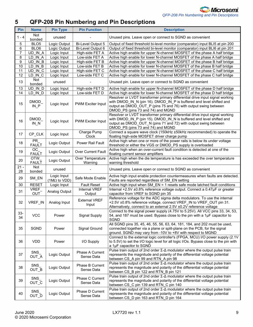
5 QFP-208 Pin Numbering and Pin Descriptions Pin Name Pin Type Pin Function Description
1 - 4 Not bonded unused - Unused pins. Leave open or connect to SGND as convenient
5 BLO5 Logic Output Bi-Level Output 5 Output of fixed threshold bi-level monitor (comparator) input BLI5 at pin 200 6 BLO6 Logic Output Bi-Level Output 6 Output of fixed threshold bi-level monitor (comparator) input BLI6 at pin 201 7 UD_IN_A Logic Input High-side FET A Active high enable for upper N-channel MOSFET of the phase A half bridge 8 LD_IN_A Logic Input Low-side FET A Active high enable for lower N-channel MOSFET of the phase A half bridge 9 UD_IN_B Logic Input High-side FET B Active high enable for upper N-channel MOSFET of the phase B half bridge 10 LD_IN_B Logic Input Low-side FET B Active high enable for lower N-channel MOSFET of the phase B half bridge 11 UD_IN_C Logic Input High-side FET C Active high enable for upper N-channel MOSFET of the phase C half bridge 12 LD_IN_C Logic Input Low-side FET C Active high enable for lower N-channel MOSFET of the phase C half bridge
13 Not bonded unused - Unused pin. Leave open or connect to SGND as convenient
13 UD_IN_D Logic Input High-side FET D Active high enable for upper N-channel MOSFET of the phase D half bridge 14 LD_IN_D Logic Input Low-side FET D Active high enable for lower N-channel MOSFET of the phase D half bridge
15 DMOD_ IN_P Logic Input PWM Exciter Input
Resolver or LVDT transformer primary differential drive input signal working with DMOD_IN_N (pin 16). DMOD_IN_P is buffered and level shifted and output as DMOD_OUT_P (pins 75 and 76) with output swing between DMOD_PS (pins 73 and 74) and MGND
16 DMOD_ IN_N Logic Input PWM Exciter Input
Resolver or LVDT transformer primary differential drive input signal working with DMOD_IN_P (pin 15). DMOD_IN_N is buffered and level shifted and output as DMOD_OUT_N (pins 71 and 72) with output swing between DMOD_PS (pins 73 and 74) and MGND
17 CP_CLK Logic Input Charge Pump Clock
Connect a square wave clock (150kHz ±50kHz recommended) to operate the floating high-side MOSFET driver charge pump
18 PR_ FAULT Logic Output Power Rail Fault Active high when one or more of the power rails is below its under voltage
threshold or either the VGS or DMOD_PS supply is overloaded
19 OC_ FAULT Logic Output Over Current Fault Active high when an over-current fault condition is detected at one of the
floating current sensor amplifiers
20 OTW_ FAULT Logic Output Over Temperature
Warning Active high when the die temperature is has exceeded the over temperature warning threshold
21 - 28
Not bonded unused - Unused pins. Leave open or connect to SGND as convenient
29 SM_EN Logic Input (1MΩ to VDD) Safe Mode Enable Active high input enable protection countermeasures when faults are detected.
Faults are reported regardless of SM_EN setting 30 RESET Logic Input Fault Reset Active high input when SM_EN = 1 resets safe mode latched fault conditions
31 VREF_ OUT Analog Output Internal VREF
Output Internal +2.5V ±0.8% reference voltage output. Connect a 0.47µF or greater capacitor from VREF to SGND pin 35
32 VREF_IN Analog Input External VREF Input
Reference voltage for the ADC sigma delta modulators. To use the internal +2.5V ±0.8% reference voltage, connect VREF_IN to VREF_OUT pin 31. Alternatively, connect to an external 2.5V ±0.2V reference voltage
33- 34 VCC Power Signal Supply
Connect to the signal power supply (4.75V to 5.25V). All VCC pins 33, 34, 53, 54, and 187 must be used. Bypass close to the pin with a 1µF capacitor to SGND
35 SGND Power Signal Ground All SGND pins 35, 45, 46, 55, 56, 63, 64, 181, 184, and 202 must be used, connected together via a plane or split-plane on the PCB, for the signal ground. SGND may vary from -10V to +8V with respect to MGND
36 VDD Power I/O Supply Connect to the external logic controller's (FPGA, MCU) I/O power supply (2.1V to 5.5V) to set the I/O logic level for all logic I/Os. Bypass close to the pin with a 1µF capacitor to SGND
37 SNS_ OUT_A Logic Output Phase A Current
Sense Data
Pulse train output of 2nd order Σ-Δ modulator where the output pulse train represents the magnitude and polarity of the differential voltage potential between CS_A pin 99 and RTN_A pin 98
38 SNS_ OUT_B Logic Output Phase B Current
Sense Data
Pulse train output of 2nd order Σ-Δ modulator where the output pulse train represents the magnitude and polarity of the differential voltage potential between CS_B pin 122 and RTN_B pin 121
39 SNS_ OUT_C Logic Output Phase C Current
Sense Data
Pulse train output of 2nd order Σ-Δ modulator where the output pulse train represents the magnitude and polarity of the differential voltage potential between CS_C pin 139 and RTN_C pin 140
40 SNS_ OUT_D Logic Output Phase D Current
Sense Data
Pulse train output of 2nd order Σ-Δ modulator where the output pulse train represents the magnitude and polarity of the differential voltage potential between CS_D pin 163 and RTN_D pin 164
Radiation Tolerant Power Driver with Four Half-Bridge Drivers, Rotation and Position Sensing
June 2020 LX7720 rev 1.1 10 © 2020 Microsemi Corporation
Pin Name Pin Type Pin Function Description
41 ADC1 Logic Output ADC 1 Data Pulse train output of 2nd order Σ-Δ modulator where the output pulse train represents the magnitude and polarity of the differential voltage potential between ADC1_P pin 62 and ADC1_N pin 61
42 ADC2 Logic Output ADC 2 Data Pulse train output of 2nd order Σ-Δ modulator where the output pulse train represents the magnitude and polarity of the differential voltage potential between ADC2_P pin 60 and ADC2_N pin 59
43 ADC3 Logic Output ADC 3 Data Pulse train output of 2nd order Σ-Δ modulator where the output pulse train represents the magnitude and polarity of the differential voltage potential between ADC3_P pin 58 and ADC3_N pin 57
44 MOD_CLK Logic Input Σ-Δ Mod Clock Connect a 24MHz to 32MHz sample rate clock for the Σ-Δ modulators
45 - 46 SGND Power Signal Ground
All SGND pins 35, 45, 46, 55, 56, 63, 64, 181, 184, and 202 must be used, connected together via a plane or split-plane on the PCB, for the signal ground. SGND may vary from -10V to +8V with respect to MGND
47 CLK_OUT Logic Output Σ-Δ Output Clock Output clock for the SNS_OUT_A, SNS_OUT_B, SNS_OUT_C, SNS_OUT_D, ADC1, ADC2, ADC3 Σ-Δ modulators, rising edge active
48 - 52
Not bonded unused - Unused pins. Leave open or connect to SGND as convenient
53 - 54 VCC Power Signal Supply
Connect to the signal power supply (4.75V to 5.25V). All VCC pins 33, 34, 53, 54, and 187 must be used. Bypass close to the pin with a 1µF capacitor to SGND
55 - 56 SGND Power Signal Ground
All SGND pins 35, 45, 46, 55, 56, 63, 64, 181, 184, and 202 must be used, connected together via a plane or split-plane on the PCB, for the signal ground. SGND may vary from -10V to +8V with respect to MGND
57 ADC3_N Analog Input 58 ADC3_P Analog Input
ADC3 differential input
ADC3_P and ADC3_N form a differential analog signal feeding into the ADC3 sigma delta modulator
59 ADC2_N Analog Input 60 ADC2_P Analog Input
ADC2 differential input
ADC2_P and ADC2_N form a differential analog signal feeding into the ADC2 sigma delta modulator
61 ADC1_N Analog Input 62 ADC1_P Analog Input
ADC1 differential input
ADC1_P and ADC1_N form a differential analog signal feeding into the ADC1 sigma delta modulator
63 - 64 SGND Power Signal Ground
All SGND pins 35, 45, 46, 55, 56, 63, 64, 181, 184, and 202 must be used, connected together via a plane or split-plane on the PCB, for the signal ground. SGND may vary from -10V to +8V with respect to MGND
65 - 68
Not bonded unused - Unused pins. Leave open or connect to SGND or MGND as convenient
69 - 70 MGND Ground Motor Ground
All MGND pins 69, 70, 77, 78, 84, 85, 101, 124, 134, 137, 161, and 177 must be used, connected together via a plane or split-plane on the PCB, for the return rail to the lower MOSFET drivers. MGND connects to the return rail of the motor and resolver/LVDT power supplies. MGND may vary from -10V to +8V with respect to SGND
71 - 72
DMOD_ OUT_N Analog Output PWM Exciter
Output
Resolver or LVDT transformer primary differential drive output working with DMOD_OUT_P (pins 75 and 76). Use both pins tied together. Input is PWM signal at DMOD_IN_N (pin 16). Output swing is between DMOD_PS (pins 73 and 74) and MGND
73 - 74 DMOD_PS Power PWM Exciter
Supply
Connect to the demodulator driver power supply (10V to 18V), typically VGS. Use both pins tied together. Bypass close to the pin with a 10µF capacitor to MGND DMOD_PS provides power to the DMOD_OUT_P (pin 46) and DMOD_OUT_N (pin 44) differential drivers
75 - 76
DMOD_ OUT_P Analog Output PWM Exciter
Output
LVDT transformer primary differential drive output working with DMOD_OUT_N (pins 71 and 72). Use both pins tied together. Input is PWM signal at DMOD_IN_P (pin 15). Output swing is between DMOD_PS (pins 73 and 74) and MGND
77 - 78 MGND Ground Motor Ground
All MGND pins 69, 70, 77, 78, 84, 85, 101, 124, 134, 137, 161, and 177 must be used, connected together via a plane or split-plane on the PCB, for the return rail to the lower MOSFET drivers. MGND connects to the return rail of the motor and resolver/LVDT power supplies. MGND may vary from -10V to +8V with respect to SGND
79 Not bonded unused - Unused pin. Leave open or connect to MGND as convenient
80 VGS Power FET Gate Drive Rail
Connect to the MOSFET gate driver power supply (10V to 18V). All VGS pins 80, 86, 108, 133, 153, and 176 must be used, connected together via a plane or split-plane on the PCB, for the power to the MOSFET drivers. Bypass close to the pin with a 1µF capacitor to MGND
81 VEE_ CP_P Output
Charge Pump Flying Capacitor
inverting
Flying capacitor positive node for the internal VEE inverting charge pump. Connect a 1µF capacitor between this pin and VEE_CP_N pin 82. VEE_CP_P swings between VMPS and VMPS + VGS
QFP-208 Pin Numbering and Pin Descriptions
June 2020 LX7720 rev 1.1 11 © 2020 Microsemi Corporation
Pin Name Pin Type Pin Function Description
82 VEE_ CP_N Output
Charge Pump Flying Capacitor
inverting
Flying capacitor negative node for the internal VEE inverting charge pump. Connect a 1µF capacitor between this pin and VEE_CP_P pin 81. VEE_CP_N swings between MGND and VEE
83 VEE Power Negative power rail
To use the internal VEE charge pump, tie EXT_VEE_EN pin 135 to VGS. Alternatively, connect an external negative supply in the range -VGS to -8V to VEE and tie EXT_VEE_EN pin 135 to MGND to disable the VEE charge pump. Connect a 2.2µF capacitor between this pin and MGND at pins 84 and 85
84 - 85 MGND Ground Motor Ground
All MGND pins 69, 70, 77, 78, 84, 85, 101, 124, 134, 137, 161, and 177 must be used, connected together via a plane or split-plane on the PCB, for the return rail to the lower MOSFET drivers. MGND connects to the return rail of the motor and resolver/LVDT power supplies. MGND may vary from -10V to +8V with respect to SGND
86 VGS_A Power FET Gate Drive Rail
Connect to the MOSFET gate driver power supply (10V to 18V). All VGS pins 80, 86, 108, 133, 153, and 176 must be used, connected together via a plane or split-plane on the PCB, for the power to the MOSFET drivers. Bypass close to the pin with a 10µF capacitor to MGND
87 - 88 LD_A FET Driver Low-side FET
Driver
Phase A lower N-channel MOSFET gate driver. Use both pins tied together. Connect through a resistor such as 20Ω to the MOSFET's gate. MGND provides the return current path
89 Not bonded unused - Unused pin. Leave open since adjacent pin can be at high voltage
90 - 91 SW_A FET Switch MOSFET Source Phase A upper N-channel MOSFET gate driver source connection. Use both
pins tied together
92 - 93 UD_A FET Driver High-side FET
Driver
Phase A upper N-channel MOSFET gate driver. Use both pins tied together. Connect through a resistor such as 20Ω to the MOSFET's gate. MGND provides the return current path
94 VFLT_A Power High-side FET Gate Drive Rail
Floating gate drive power rail for upper N-channel MOSFET gate driver A. Bypass close to the pin with a 1µF capacitor to SW_A. Connect a silicon or Schottky diode such as 1N5809US, 1N5811US or 1N6864US between VFLT_A and VGS_A pin 86
95 Not bonded unused - Unused pin. Leave open since adjacent pin can be at high voltage
96 CSPS_A Power Phase A Current Sense Supply
Power to phase A floating current sense. Connect to either VFLT_A pin 94 for SW_A sensing or to VGS for low-side sensing. Connect a 1µF capacitor between this pin and RTN_A pin 98
97 Not bonded unused - Unused pin. Leave open since adjacent pin can be at high voltage
98 RTN_A Signal/Power Phase A Current Sense Return
Ground reference for phase A floating current sense and current measurement power rail
99 CS_A Analog Input Phase A current sense
Current measurement input for phase A floating current sensing, with a ±200mV linear range across the phase A sense resistor
100 Not bonded unused - Unused pin. Leave open since adjacent pin can be at high voltage
101 MGND Ground Motor Ground
All MGND pins 69, 70, 77, 78, 84, 85, 101, 124, 134, 137, 161, and 177 must be used, connected together via a plane or split-plane on the PCB, for the return rail to the lower MOSFET drivers. MGND connects to the return rail of the motor and resolver/LVDT power supplies. MGND may vary from -10V to +8V with respect to SGND
102 - 107
Not bonded unused - Unused pins. Leave open or connect to MGND as convenient
108 VGS_B Power FET Gate Drive Rail
Connect to the MOSFET gate driver power supply (10V to 18V). All VGS pins 80, 86, 108, 133, 153, and 176 must be used, connected together via a plane or split-plane on the PCB, for the power to the MOSFET drivers. Bypass close to the pin with a 10µF capacitor to MGND
109 - 110 LD_B FET Driver Low-side FET
Driver
Phase B lower N-channel MOSFET gate driver. Use both pins tied together. Connect through a resistor such as 20Ω to the MOSFET's gate. MGND provides the return current path
111 Not bonded unused - Unused pin. Leave open since adjacent pin can be at high voltage
112 - 113 SW_B FET Switch MOSFET Source Phase B upper N-channel MOSFET gate driver source connection. Use both
pins tied together
114 - 115 UD_B FET Driver High-side FET
Driver
Phase B upper N-channel MOSFET gate driver. Use both pins tied together. Connect through a resistor such as 20Ω to the MOSFET's gate. MGND provides the return current path
Radiation Tolerant Power Driver with Four Half-Bridge Drivers, Rotation and Position Sensing
June 2020 LX7720 rev 1.1 12 © 2020 Microsemi Corporation
Pin Name Pin Type Pin Function Description
116 Not bonded unused - Unused pin. Leave open since adjacent pin can be at high voltage
117 VFLT_B Power High-side FET Gate Drive Rail
Floating gate drive power rail for upper N-channel MOSFET gate driver B. Bypass close to the pin with a 1µF capacitor to SW_B. Connect a silicon or Schottky diode such as 1N5809US, 1N5811US or 1N6864US between VFLT_B and VGS_B pin 108
118 Not bonded unused - Unused pin. Leave open since adjacent pin can be at high voltage
119 CSPS_B Power Phase B Current Sense Supply
Power to phase B floating current sense. Connect to either VFLT_B pin 117 for SW_B sensing or to VGS for low-side sensing. Connect a 1µF capacitor between this pin and RTN_B pin 121
120 Not bonded unused - Unused pin. Leave open since adjacent pin can be at high voltage
121 RTN_B Signal/Power Phase B Current Sense Return
Ground reference for phase B floating current sense and current measurement power rail
122 CS_B Analog Input Phase B current sense
Current measurement input for phase B floating current sensing, with a ±200mV linear range across the phase B sense resistor
123 Not bonded unused - Unused pin. Leave open since adjacent pin can be at high voltage
124 MGND Ground Motor Ground
All MGND pins 69, 70, 77, 78, 84, 85, 101, 124, 134, 137, 161, and 177 must be used, connected together via a plane or split-plane on the PCB, for the return rail to the lower MOSFET drivers. MGND connects to the return rail of the motor and resolver/LVDT power supplies. MGND may vary from -10V to +8V with respect to SGND
125 Not bonded unused - Unused pin. Leave open since adjacent pin can be at high voltage
126 VMPS Power Motor Power supply
Motor power rail, used for the upper MOSFET drivers charge pump, VBOOST pin 130. Connect a 1µF capacitor between this pin and MGND
127 Not bonded unused - Unused pin. Leave open since adjacent pin can be at high voltage
128 CPP Output Charge Pump
Flying Capacitor inverting
Flying capacitor negative node for the internal VBOOST charge pump. Connect a 0.47µF capacitor between this pin and CPN pin 132. CPP swings between VMPS and (VMPS + VGS)
129 Not bonded unused - Unused pin. Leave open since adjacent pin can be at high voltage
130 VBOOST Power Upper MOSFET Driver Charge
Pump
Charge pump output which is VGS volts above VMPS, unloaded. Connect a 1µF capacitor between this pin and VMPS pin 126
131 Not bonded unused - Unused pin. Leave open since adjacent pin can be at high voltage
132 CPN Output Charge Pump
Flying Capacitor inverting
Flying capacitor negative node for the internal VBOOST charge pump. Connect a 0.47µF capacitor between this pin and CPP pin 128. CPN swings between MGND and VGS
133 VGS Power FET Gate Drive Rail
Connect to the MOSFET gate driver power supply (10V to 18V). All VGS pins 80, 86, 108, 133, 153, and 176 must be used, connected together via a plane or split-plane on the PCB, for the power to the MOSFET drivers. Bypass close to the pin with a 1µF capacitor to MGND
134 MGND Ground Motor Ground
All MGND pins 69, 70, 77, 78, 84, 85, 101, 124, 134, 137, 161, and 177 must be used, connected together via a plane or split-plane on the PCB, for the return rail to the lower MOSFET drivers. MGND connects to the return rail of the motor and resolver/LVDT power supplies. MGND may vary from -10V to +8V with respect to SGND
135 EXT_VEE_EN
Control Input (1MΩ to VGS)
External VEE Enable
Active high (leave open or tie to VGS) to enable the VEE charge pump. Connect to MGND to disable the VEE charge pump, and connect a negative supply in the range -VGS to -8V to VEE pin 83
136 Not bonded unused - Unused pin. Leave open or connect to MGND as convenient
137 MGND Ground Motor Ground
All MGND pins 69, 70, 77, 78, 84, 85, 101, 124, 134, 137, 161, and 177 must be used, connected together via a plane or split-plane on the PCB, for the return rail to the lower MOSFET drivers. MGND connects to the return rail of the motor and resolver/LVDT power supplies. MGND may vary from -10V to +8V with respect to SGND
138 Not bonded unused - Unused pin. Leave open since adjacent pin can be at high voltage
QFP-208 Pin Numbering and Pin Descriptions
June 2020 LX7720 rev 1.1 13 © 2020 Microsemi Corporation
Pin Name Pin Type Pin Function Description
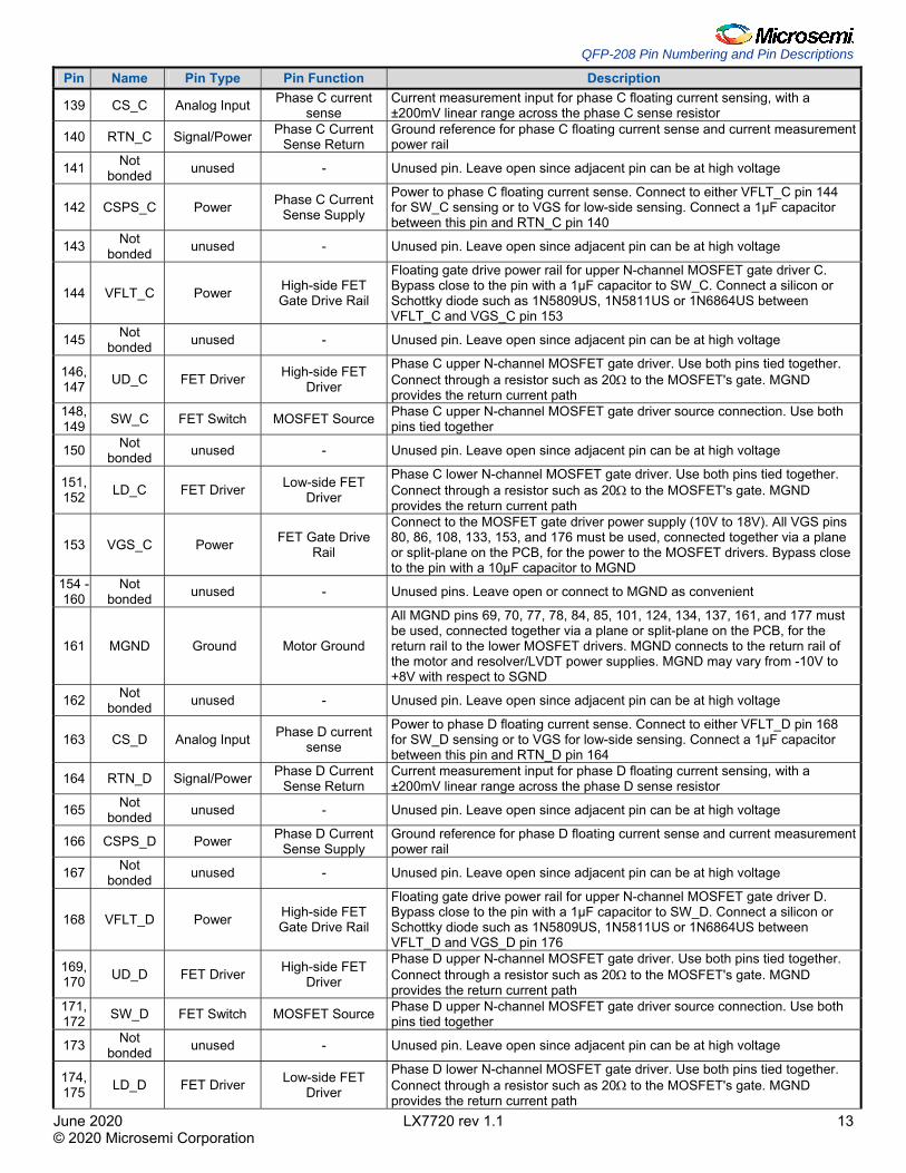
139 CS_C Analog Input Phase C current sense
Current measurement input for phase C floating current sensing, with a ±200mV linear range across the phase C sense resistor
140 RTN_C Signal/Power Phase C Current Sense Return
Ground reference for phase C floating current sense and current measurement power rail
141 Not bonded unused - Unused pin. Leave open since adjacent pin can be at high voltage
142 CSPS_C Power Phase C Current Sense Supply
Power to phase C floating current sense. Connect to either VFLT_C pin 144 for SW_C sensing or to VGS for low-side sensing. Connect a 1µF capacitor between this pin and RTN_C pin 140
143 Not bonded unused - Unused pin. Leave open since adjacent pin can be at high voltage
144 VFLT_C Power High-side FET Gate Drive Rail
Floating gate drive power rail for upper N-channel MOSFET gate driver C. Bypass close to the pin with a 1µF capacitor to SW_C. Connect a silicon or Schottky diode such as 1N5809US, 1N5811US or 1N6864US between VFLT_C and VGS_C pin 153
145 Not bonded unused - Unused pin. Leave open since adjacent pin can be at high voltage
146, 147 UD_C FET Driver High-side FET
Driver
Phase C upper N-channel MOSFET gate driver. Use both pins tied together. Connect through a resistor such as 20Ω to the MOSFET's gate. MGND provides the return current path
148, 149 SW_C FET Switch MOSFET Source Phase C upper N-channel MOSFET gate driver source connection. Use both
pins tied together
150 Not bonded unused - Unused pin. Leave open since adjacent pin can be at high voltage
151, 152 LD_C FET Driver Low-side FET
Driver
Phase C lower N-channel MOSFET gate driver. Use both pins tied together. Connect through a resistor such as 20Ω to the MOSFET's gate. MGND provides the return current path
153 VGS_C Power FET Gate Drive Rail
Connect to the MOSFET gate driver power supply (10V to 18V). All VGS pins 80, 86, 108, 133, 153, and 176 must be used, connected together via a plane or split-plane on the PCB, for the power to the MOSFET drivers. Bypass close to the pin with a 10µF capacitor to MGND
154 - 160
Not bonded unused - Unused pins. Leave open or connect to MGND as convenient
161 MGND Ground Motor Ground
All MGND pins 69, 70, 77, 78, 84, 85, 101, 124, 134, 137, 161, and 177 must be used, connected together via a plane or split-plane on the PCB, for the return rail to the lower MOSFET drivers. MGND connects to the return rail of the motor and resolver/LVDT power supplies. MGND may vary from -10V to +8V with respect to SGND
162 Not bonded unused - Unused pin. Leave open since adjacent pin can be at high voltage
163 CS_D Analog Input Phase D current sense
Power to phase D floating current sense. Connect to either VFLT_D pin 168 for SW_D sensing or to VGS for low-side sensing. Connect a 1µF capacitor between this pin and RTN_D pin 164
164 RTN_D Signal/Power Phase D Current Sense Return
Current measurement input for phase D floating current sensing, with a ±200mV linear range across the phase D sense resistor
165 Not bonded unused - Unused pin. Leave open since adjacent pin can be at high voltage
166 CSPS_D Power Phase D Current Sense Supply
Ground reference for phase D floating current sense and current measurement power rail
167 Not bonded unused - Unused pin. Leave open since adjacent pin can be at high voltage
168 VFLT_D Power High-side FET Gate Drive Rail
Floating gate drive power rail for upper N-channel MOSFET gate driver D. Bypass close to the pin with a 1µF capacitor to SW_D. Connect a silicon or Schottky diode such as 1N5809US, 1N5811US or 1N6864US between VFLT_D and VGS_D pin 176
169, 170 UD_D FET Driver High-side FET
Driver
Phase D upper N-channel MOSFET gate driver. Use both pins tied together. Connect through a resistor such as 20Ω to the MOSFET's gate. MGND provides the return current path
171, 172 SW_D FET Switch MOSFET Source Phase D upper N-channel MOSFET gate driver source connection. Use both
pins tied together
173 Not bonded unused - Unused pin. Leave open since adjacent pin can be at high voltage
174, 175 LD_D FET Driver Low-side FET
Driver
Phase D lower N-channel MOSFET gate driver. Use both pins tied together. Connect through a resistor such as 20Ω to the MOSFET's gate. MGND provides the return current path
Radiation Tolerant Power Driver with Four Half-Bridge Drivers, Rotation and Position Sensing
June 2020 LX7720 rev 1.1 14 © 2020 Microsemi Corporation
Pin Name Pin Type Pin Function Description
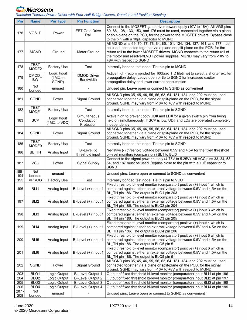
176 VGS_D Power FET Gate Drive Rail
Connect to the MOSFET gate driver power supply (10V to 18V). All VGS pins 80, 86, 108, 133, 153, and 176 must be used, connected together via a plane or split-plane on the PCB, for the power to the MOSFET drivers. Bypass close to the pin with a 10µF capacitor to MGND
177 MGND Ground Motor Ground
All MGND pins 69, 70, 77, 78, 84, 85, 101, 124, 134, 137, 161, and 177 must be used, connected together via a plane or split-plane on the PCB, for the return rail to the lower MOSFET drivers. MGND connects to the return rail of the motor and resolver/LVDT power supplies. MGND may vary from -10V to +8V with respect to SGND
178 TEST MODE2 Factory Use Test Internally bonded test node. Tie this pin to MGND
179 DMOD_ BW
Logic Input (1MΩ to SGND)
DMOD Driver Bandwidth
Active high (recommended for 100krad TID lifetime) to select a shorter exciter propagation delay. Leave open or tie to SGND for increased exciter propagation delay and lower current consumption
180 Not bonded unused - Unused pin. Leave open or connect to SGND as convenient
181 SGND Power Signal Ground All SGND pins 35, 45, 46, 55, 56, 63, 64, 181, 184, and 202 must be used, connected together via a plane or split-plane on the PCB, for the signal ground. SGND may vary from -10V to +8V with respect to MGND
182 TEST MODE1 Factory Use Test Internally bonded test node. Tie this pin to SGND
183 SCP Logic Input (1MΩ to VDD)
Simultaneous Conduction Protection
Active high to prevent both UD# and LD# for a given switch pin from being held on simultaneously. If SCP is low, UD# and LD# are operated completely independently
184 SGND Power Signal Ground All SGND pins 35, 45, 46, 55, 56, 63, 64, 181, 184, and 202 must be used, connected together via a plane or split-plane on the PCB, for the signal ground. SGND may vary from -10V to +8V with respect to MGND
185 TEST MODE0 Factory Use Test Internally bonded test node. Tie this pin to SGND
186 BL_TH Analog Input Bi-Level (-) threshold input
Negative (-) threshold voltage between 0.5V and 4.5V for the fixed threshold bi-level monitors (comparators) BL1 to BLI6
187 VCC Power Signal Supply Connect to the signal power supply (4.75V to 5.25V). All VCC pins 33, 34, 53, 54, and 187 must be used. Bypass close to the pin with a 1µF capacitor to SGND
188 - 194
Not bonded unused - Unused pins. Leave open or connect to SGND as convenient
195 VPROG Factory Use Test Internally bonded test node. Tie this pin to VCC
196 BLI1 Analog Input Bi-Level (+) input 1Fixed threshold bi-level monitor (comparator) positive (+) input 1 which is compared against either an external voltage between 0.5V and 4.5V on the BL_TH pin 186. The output is BLO1 pin 203
197 BLI2 Analog Input Bi-Level (+) input 1Fixed threshold bi-level monitor (comparator) positive (+) input 2 which is compared against either an external voltage between 0.5V and 4.5V on the BL_TH pin 186. The output is BLO2 pin 204
198 BLI3 Analog Input Bi-Level (+) input 1Fixed threshold bi-level monitor (comparator) positive (+) input 3 which is compared against either an external voltage between 0.5V and 4.5V on the BL_TH pin 186. The output is BLO3 pin 205
199 BLI4 Analog Input Bi-Level (+) input 1Fixed threshold bi-level monitor (comparator) positive (+) input 4 which is compared against either an external voltage between 0.5V and 4.5V on the BL_TH pin 186. The output is BLO4 pin 206
200 BLI5 Analog Input Bi-Level (+) input 1Fixed threshold bi-level monitor (comparator) positive (+) input 5 which is compared against either an external voltage between 0.5V and 4.5V on the BL_TH pin 186. The output is BLO5 pin 5
201 BLI6 Analog Input Bi-Level (+) input 1Fixed threshold bi-level monitor (comparator) positive (+) input 6 which is compared against either an external voltage between 0.5V and 4.5V on the BL_TH pin 186. The output is BLO5 pin 6
202 SGND Power Signal Ground All SGND pins 35, 45, 46, 55, 56, 63, 64, 181, 184, and 202 must be used, connected together via a plane or split-plane on the PCB, for the signal ground. SGND may vary from -10V to +8V with respect to MGND
203 BLO1 Logic Output Bi-Level Output 1 Output of fixed threshold bi-level monitor (comparator) input BLI1 at pin 196 204 BLO2 Logic Output Bi-Level Output 2 Output of fixed threshold bi-level monitor (comparator) input BLI2 at pin 197 205 BLO3 Logic Output Bi-Level Output 3 Output of fixed threshold bi-level monitor (comparator) input BLI3 at pin 198 206 BLO4 Logic Output Bi-Level Output 4 Output of fixed threshold bi-level monitor (comparator) input BLI4 at pin 199
207 - 208
Not bonded unused - Unused pins. Leave open or connect to SGND as convenient
Absolute Maximum Ratings
June 2020 LX7720 rev 1.1 15 © 2020 Microsemi Corporation
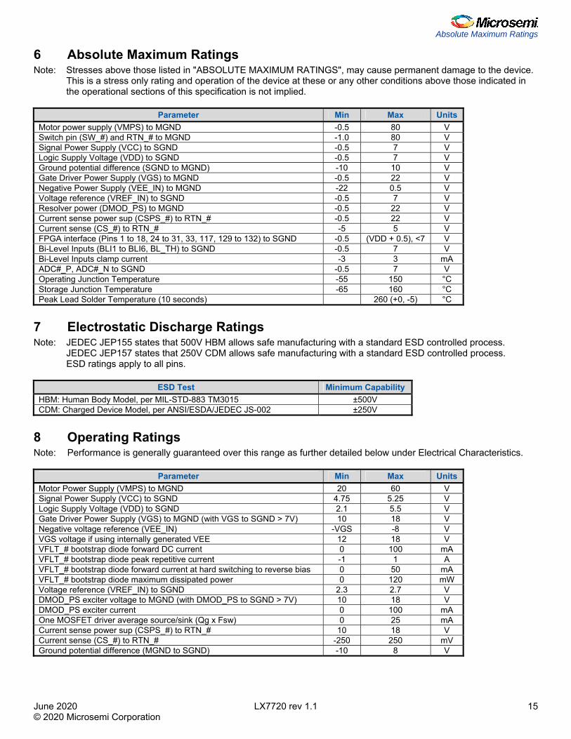
6 Absolute Maximum Ratings Note: Stresses above those listed in "ABSOLUTE MAXIMUM RATINGS", may cause permanent damage to the device.
This is a stress only rating and operation of the device at these or any other conditions above those indicated in the operational sections of this specification is not implied.
Parameter Min Max Units
Motor power supply (VMPS) to MGND -0.5 80 V Switch pin (SW_#) and RTN_# to MGND -1.0 80 V Signal Power Supply (VCC) to SGND -0.5 7 V Logic Supply Voltage (VDD) to SGND -0.5 7 V Ground potential difference (SGND to MGND) -10 10 V Gate Driver Power Supply (VGS) to MGND -0.5 22 V Negative Power Supply (VEE_IN) to MGND -22 0.5 V Voltage reference (VREF_IN) to SGND -0.5 7 V Resolver power (DMOD_PS) to MGND -0.5 22 V Current sense power sup (CSPS_#) to RTN_# -0.5 22 V Current sense (CS_#) to RTN_# -5 5 V FPGA interface (Pins 1 to 18, 24 to 31, 33, 117, 129 to 132) to SGND -0.5 (VDD + 0.5), <7 V Bi-Level Inputs (BLI1 to BLI6, BL_TH) to SGND -0.5 7 V Bi-Level Inputs clamp current -3 3 mA ADC#_P, ADC#_N to SGND -0.5 7 V Operating Junction Temperature -55 150 °C Storage Junction Temperature -65 160 °C Peak Lead Solder Temperature (10 seconds) 260 (+0, -5) °C
7 Electrostatic Discharge Ratings Note: JEDEC JEP155 states that 500V HBM allows safe manufacturing with a standard ESD controlled process.
JEDEC JEP157 states that 250V CDM allows safe manufacturing with a standard ESD controlled process. ESD ratings apply to all pins.
ESD Test Minimum Capability
HBM: Human Body Model, per MIL-STD-883 TM3015 ±500V CDM: Charged Device Model, per ANSI/ESDA/JEDEC JS-002 ±250V
8 Operating Ratings Note: Performance is generally guaranteed over this range as further detailed below under Electrical Characteristics.
Parameter Min Max Units Motor Power Supply (VMPS) to MGND 20 60 V Signal Power Supply (VCC) to SGND 4.75 5.25 V Logic Supply Voltage (VDD) to SGND 2.1 5.5 V Gate Driver Power Supply (VGS) to MGND (with VGS to SGND > 7V) 10 18 V Negative voltage reference (VEE_IN) -VGS -8 V VGS voltage if using internally generated VEE 12 18 V VFLT_# bootstrap diode forward DC current 0 100 mA VFLT_# bootstrap diode peak repetitive current -1 1 A VFLT_# bootstrap diode forward current at hard switching to reverse bias 0 50 mA VFLT_# bootstrap diode maximum dissipated power 0 120 mW Voltage reference (VREF_IN) to SGND 2.3 2.7 V DMOD_PS exciter voltage to MGND (with DMOD_PS to SGND > 7V) 10 18 V DMOD_PS exciter current 0 100 mA One MOSFET driver average source/sink (Qg x Fsw) 0 25 mA Current sense power sup (CSPS_#) to RTN_# 10 18 V Current sense (CS_#) to RTN_# -250 250 mV Ground potential difference (MGND to SGND) -10 8 V
Radiation Tolerant Power Driver with Four Half-Bridge Drivers, Rotation and Position Sensing
June 2020 LX7720 rev 1.1 16 © 2020 Microsemi Corporation
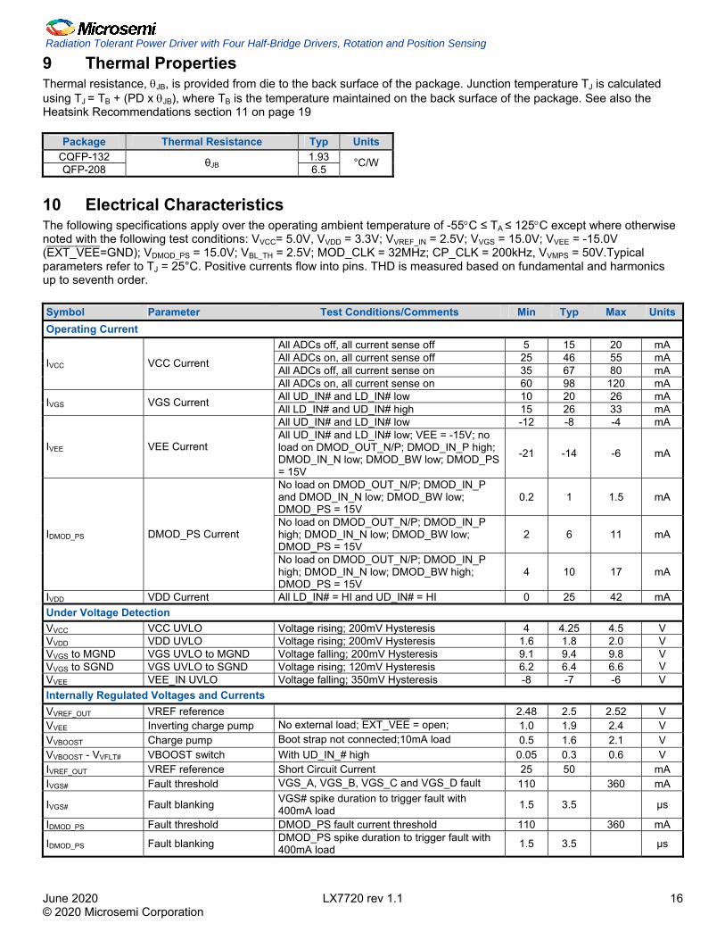
9 Thermal Properties Thermal resistance, θJB, is provided from die to the back surface of the package. Junction temperature TJ is calculated using TJ = TB + (PD x θJB), where TB is the temperature maintained on the back surface of the package. See also the Heatsink Recommendations section 11 on page 19
Package Thermal Resistance Typ Units CQFP-132 1.93 QFP-208 θJB 6.5 °C/W
10 Electrical Characteristics The following specifications apply over the operating ambient temperature of -55°C ≤ TA ≤ 125°C except where otherwise noted with the following test conditions: VVCC= 5.0V, VVDD = 3.3V; VVREF_IN = 2.5V; VVGS = 15.0V; VVEE = -15.0V (EXT_VEE=GND); VDMOD_PS = 15.0V; VBL_TH = 2.5V; MOD_CLK = 32MHz; CP_CLK = 200kHz, VVMPS = 50V.Typical parameters refer to TJ = 25°C. Positive currents flow into pins. THD is measured based on fundamental and harmonics up to seventh order. Symbol Parameter Test Conditions/Comments Min Typ Max Units Operating Current
All ADCs off, all current sense off 5 15 20 mA All ADCs on, all current sense off 25 46 55 mA All ADCs off, all current sense on 35 67 80 mA IVCC VCC Current
All ADCs on, all current sense on 60 98 120 mA All UD_IN# and LD_IN# low 10 20 26 mA IVGS VGS Current All LD_IN# and UD_IN# high 15 26 33 mA All UD_IN# and LD_IN# low -12 -8 -4 mA
IVEE VEE Current All UD_IN# and LD_IN# low; VEE = -15V; no load on DMOD_OUT_N/P; DMOD_IN_P high; DMOD_IN_N low; DMOD_BW low; DMOD_PS = 15V
-21 -14 -6 mA
No load on DMOD_OUT_N/P; DMOD_IN_P and DMOD_IN_N low; DMOD_BW low; DMOD_PS = 15V
0.2 1 1.5 mA
No load on DMOD_OUT_N/P; DMOD_IN_P high; DMOD_IN_N low; DMOD_BW low; DMOD_PS = 15V
2 6 11 mA IDMOD_PS DMOD_PS Current
No load on DMOD_OUT_N/P; DMOD_IN_P high; DMOD_IN_N low; DMOD_BW high; DMOD_PS = 15V
4 10 17 mA
IVDD VDD Current All LD_IN# = HI and UD_IN# = HI 0 25 42 mA Under Voltage Detection VVCC VCC UVLO Voltage rising; 200mV Hysteresis 4 4.25 4.5 V VVDD VDD UVLO Voltage rising; 200mV Hysteresis 1.6 1.8 2.0 V VVGS to MGND VGS UVLO to MGND Voltage falling; 200mV Hysteresis 9.1 9.4 9.8 VVGS to SGND VGS UVLO to SGND Voltage rising; 120mV Hysteresis 6.2 6.4 6.6
V V
VVEE VEE_IN UVLO Voltage falling; 350mV Hysteresis -8 -7 -6 V Internally Regulated Voltages and Currents VVREF_OUT VREF reference 2.48 2.5 2.52 V VVEE Inverting charge pump No external load; EXT_VEE = open; 1.0 1.9 2.4 V VVBOOST Charge pump Boot strap not connected;10mA load 0.5 1.6 2.1 V VVBOOST - VVFLT# VBOOST switch With UD_IN_# high 0.05 0.3 0.6 V IVREF_OUT VREF reference Short Circuit Current 25 50 mA IVGS# Fault threshold VGS_A, VGS_B, VGS_C and VGS_D fault 110 360 mA
IVGS# Fault blanking VGS# spike duration to trigger fault with 400mA load 1.5 3.5 µs
IDMOD_PS Fault threshold DMOD_PS fault current threshold 110 360 mA
IDMOD_PS Fault blanking DMOD_PS spike duration to trigger fault with 400mA load 1.5 3.5 µs
Electrical Characteristics
June 2020 LX7720 rev 1.1 17 © 2020 Microsemi Corporation
Symbol Parameter Test Conditions/Comments Min Typ Max Units MOSFET DRIVER (Cload = 1000pF)
VFLT# to UD_#; UD_IN_# = high 0.85 10.0 UD_# to SW_#; UD_IN_# = low 0.85 10.0 RUD# Upper driver impedance UD_# to SW_#, VGS = 0 to UVLO 20k
Ω
VGS_OUT to UD_#; LD_IN_# = high 0.85 10.0 LD_# to MGND; LD_IN_# = low 0.85 10.0 RLD# Lower driver impedance LD_# to MGND; VGS = 0 to UVLO 20k
Ω
Upper Driver; UD_IN_# to UD_A 140 250 400 Lower Driver; LD_IN_# to LD_A 140 250 400 tPHL, PLH Propagation delay Matching all drivers, all edges 150
ns
tR,F Rise time and fall time 10% to 90% 20 60 120 ns
tPWH, tPWL Minimum input pulse width (high or low)
Output reaches 67% VGS for tPWH and 1V for for tPWL
300 ns
IUD# Leakage current with VGS and VCC = 0V
UD_#, SW_#, VFLT_# wired together; VSW_# = 0V to 80V ref to MGND -50 50 µA
VUD# Upper drive voltage with 100% duty cycle
UD_IN# held high, UD_# loaded with 4mA. Measured relative to VMPS 11.5 15 V
dVSW/dt Max SW_# slew rate 10 kV/µs Internal bootstrap diodes VON_B Forward voltage IF = 100mA, Tj = 25°C 0.9 1.1 V VON_B Forward voltage IF = 100mA, Tj = -55°C and 125°C 0.8 1.2 V tRR_B Reverse recovery time IF = 100mA, VR=9V, dIF/dt = 1A/µs 600 ns IRM_B Peak reverse recovery IF = 100mA, VR=9V, dIF/dt = 1A/µs 90 mA ADC Converters (with sinc3 filter and OSR = 256, input common mode = 2.1V unless otherwise specified) FSRADC_# Max differential input Extrapolated Clipping points of PDM output ±1400 mV SLRADC_# Specified linear range ±800 mV
VCMR_ADC_# Input common mode With Vdiff = ±800mV and THD < THD24/32ADC(Max) - 3dB 0.5 VCC-
2.1V V
VCMR_ADC_# Common mode rejection 0.5V to 2.9V 43 dB Max frequency With attenuation < 0.1dB 20 kHz BWADC_# Min frequency By design 0 Hz
Tj = 25°C and 125°C -0.65 0.65 % AVADC_# Gain error Tj = -55°C -0.8 0.8 % Equivalent input for code measured to shorted inputs. Tj = 25°C -0.05 0.05 %FSR
Equivalent input for code measured to shorted inputs. Tj = 125°C -0.12 0.12 %FSRVOS_ADC Offset error
Equivalent input for code measured to shorted inputs. Tj = -55°C -0.5 0.5 %FSR
INL24ADC Integral Non-Linearity Gain error from straight line at 24MHz -0.03 ±0.01 0.03 %FSRINL32ADC Integral Non-Linearity Gain error from straight line at 32MHz -0.06 ±0.02 0.06 %FSR
RES24ADC No missing codes resolution at 24MHz Histogram test using triangular wave 14 15 bits
RES32ADC No missing codes resolution at 32MHz Histogram test using triangular wave 13 14 bits
SNR24ADC Signal to Noise Ratio at 24MHz clock
Full scale sinewave RMS / noise RMS in 1kHz bandwidth 93 100 dB
THD24ADC Total Harmonic Distortion at 24MHz clock Input frequency = 1kHz, amplitude = 800mV -79 -73 dB
SNR32ADC Signal to Noise Ratio at 32MHz clock
Full scale sinewave RMS / noise RMS in 1kHz bandwidth 92 98 dB
THD32ADC Total Harmonic Distortion at 32MHz clock Input frequency = 1kHz, amplitude = 800mV -78 -70 dB
tSWTO ADC Timeout ADC#_P= ADC#_N > VSWTO to cause ADC modulator sleep mode 225 325 µs
VSWTO ADC timeout threshold VCC - 0.25
VCC -0.1 VCC V
CADC# Diff input capacitance 10 pF RADC# Diff input resistance 50 250 kΩ
Radiation Tolerant Power Driver with Four Half-Bridge Drivers, Rotation and Position Sensing
June 2020 LX7720 rev 1.1 18 © 2020 Microsemi Corporation
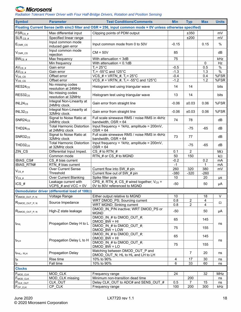
Symbol Parameter Test Conditions/Comments Min Typ Max Units Floating Current Sense (with sinc3 filter and OSR = 256, input common mode = 0V unless otherwise specified) FSRCS_# Max differential input Clipping points of PDM output ±350 mV SLR CS_# Specified linear range ±200 mV
ECMR_CS Input common mode induced gain error Input common mode from 0 to 50V -0.15 0.15 %
VCMR_CS Input common mode rejection CM = 50V 85 dB
BWCS_# Max frequency With attenuation < 3dB 75 kHz Min frequency With attenuation < 0.1dB 0 Hz AVCS_# Gain error Tj = 25°C -0.5 0.5 % AVCS_# Gain error Tj = -55°C and 125°C -1.3 1.3 % VOS_CS Offset error VCS_# = VRTN_#, Tj = 25°C -0.4 0.4 %FSRVOS_CS Offset error VCS_# = VRTN_#, Tj = -55°C and 125°C -1.2 1.2 %FSR
RES24CS No missing codes resolution at 24MHz Histogram test using triangular wave 14 14 bits
RES32CS No missing codes resolution at 32MHz Histogram test using triangular wave 13 14 bits
INL24CS Integral Non-Linearity at 24MHz clock. Gain error from straight line -0.06 ±0.03 0.06 %FSR
INL32CS Integral Non-Linearity at 32MHz clock. Gain error from straight line -0.06 ±0.03 0.06 %FSR
SNR24CS Signal to Noise Ratio at 24MHz clock
Full scale sinewave RMS / noise RMS in 4kHz bandwidth, OSR = 64 74 78 dB
THD24CS Total Harmonic Distortion at 24MHz clock
Input frequency = 1kHz, amplitude = 200mV, OSR = 64 -75 -65 dB
SNR32CS Signal to Noise Ratio at 32MHz clock
Full scale sinewave RMS / noise RMS in 4kHz bandwidth, OSR = 64 73 77 dB
THD32CS Total Harmonic Distortion at 32MHz clock
Input frequency = 1kHz, amplitude = 200mV, OSR = 64 -75 -65 dB
ZIN_CS Differential Input Imped. CS_# to RTN_# 0.1 2 MΩ Common mode RTN_# or CS_# to MGND 50 150 kΩ IBIAS_CS# CS_# bias current -0.2 0.2 mA IBIAS_RTN# RTN_# bias current -1 1 mA
Current flow into SW_# pin 260 320 380 mV VCS_# Over Current Sense Threshold Current flow out of SW_# pin -380 -320 -260
VCS_# Over Current Blanking Spike filter pole 10 20 µs
ICS_# Leakage current with VCPS_# and VCC = 0V
CPS_#, RTN_#, CS_# wired together; VCS = 0V to 80V referenced to MGND -50 50 µA
Demodulator driver (differential load of 100Ω) VDMOD_OUT_P, N Voltage Range Either output relative to MGND 10 18 V
WRT DMOD_PS; Sourcing current 0.8 2 4 RDMOD_OUT_P, N Source Impedance WRT MGND; Sinking current 0.8 2 4 Ω
RDMOD_OUT_P, N High-Z state leakage DMOD_IN_P/N inactive; WRT DMOD_PS or MGND -50 50 µA
DMOD_IN_# to DMOD_OUT_#; DMOD_BW = HI 65 145
tPHL Propagation Delay H to L DMOD_IN_# to DMOD_OUT_#; DMOD_BW = LOW 75 155
ns
DMOD_IN_# to DMOD_OUT_#; DMOD_BW = HI 65 145
tPLH Propagation Delay L to H DMOD_IN_# to DMOD_OUT_#; DMOD_BW = LO 75 155
ns
tPHL, PLH Propagation Delay Matching between DMOD_OUT_P and DMOD_OUT_N; HL to HL and LH to LH 7 20 ns
tR Rise time 10% to 90% 4 17 30 ns tF Fall time 10% to 90% 6 33 60 ns Clocks FMOD_CLK MOD_CLK Frequency range 24 32 MHz FMOD_CLK MOD_CLK missing Minimum non-transition dead time 200 ns PCLK_OUT CLK_OUT Delay CLK_OUT to ADC# and SENS_OUT_# 0.5 7 15 ns FCP_CLK CP_CLK Frequency range 100 200 300 kHz
Heatsink Recommendations
June 2020 LX7720 rev 1.1 19 © 2020 Microsemi Corporation
Symbol Parameter Test Conditions/Comments Min Typ Max Units Logic Levels
VIH 70 %VDD
VIL 30 %VDDVLOG_IN VDD
Input logic threshold for VDD related inputs: UD_IN_#, DMOD_IN_#, SM_EN, RESET, MOD_CLK, SCP Hysteresis at VDD = 3.3V 100 160 220 mV
VLOG_IN = 3.3V (with pull down resistor) 4 7 ILOG_IN VDD
Input current for above VDD related inputs VLOG_IN = 0V (with pull up resistor) -7 -4 µA
VIH 1.2 VLOG_IN EXT_VEE
Input logic threshold for EXT_VEE VIL 0.25 V
ILOG_IN EXT_VEE
Input current for EXT_VEE VLOG_IN = 0V -80 -38 -10 µA
VIH 1.8 VLOG_IN DMOD_BW
Input logic threshold for DMOD_BW VIL 0.4 V
VLOG_IN = 3.3V 10 37 80 ILOG_IN DMOD_BW
Input current for DMOD_BW VLOG_IN = 0V -1 0 1 µA
High logic level (100µA source) VDD -0.3 VDD
VLOG_OUT VDD
Logic output levels for VDD related outputs: BLO_#, PR_FAULT, OC_FAULT, CLK_OUT, SNS_OUT_#, ADC#
Low logic level (100µA sink) 0 0.3 V
Fixed Threshold Bi-Level Inputs VBL_TH# Threshold, rising voltage 2.4 2.5 2.6 V
VBL_HYS# Hysteresis Rising threshold = VBL_TH# Falling threshold = (VBL_TH# - VBL_HYS#)
80 150 200 mV
Clamp Current = 1mA into pin 6.5 10 13 VBLI# Voltage Clamp
Clamp Current = -1mA out of pin -1.9 -1.4 -0.9 V
IBLI# Bias Current Clamp Current = 1mA into pin -2 0 2 µA IBLI# Leakage Current VBLI1 = 0V to 5V -1 0 1.2 µA tBLI# Propagation Delay VBLI1 = 0V to 5V; IC powered off 10 40 80 ns IBL_TH Threshold Pin Leakage VBL_TH= 0V to 5V -1 0 1.5 µA Thermal Shutdown
OT_SDN Thermal shutdown threshold; SM_EN = 1 Threshold Temperature 135 150 165
Warning Temperature (TSD - TOTW) 15 25 35 Over temperature warning threshold Hysteresis 10 15 25
°C
High logic level (100µA source) VDD -0.3 VDD OTW_FAULT Logic output levels. Logic
low level is untested at 125°C because output is typically high at 125°C Low logic level (100µA sink) 0 0.3
V
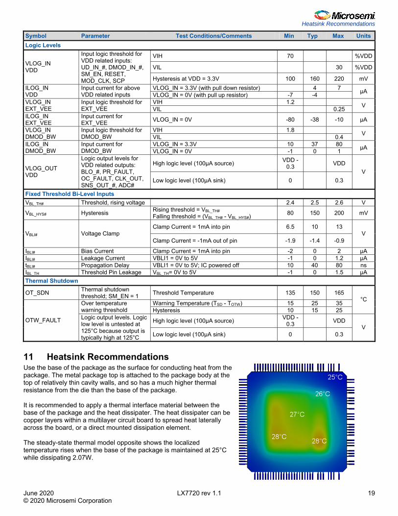
11 Heatsink Recommendations Use the base of the package as the surface for conducting heat from the package. The metal package top is attached to the package body at the top of relatively thin cavity walls, and so has a much higher thermal resistance from the die than the base of the package. It is recommended to apply a thermal interface material between the base of the package and the heat dissipater. The heat dissipater can be copper layers within a multilayer circuit board to spread heat laterally across the board, or a direct mounted dissipation element. The steady-state thermal model opposite shows the localized temperature rises when the base of the package is maintained at 25°C while dissipating 2.07W.
Radiation Tolerant Power Driver with Four Half-Bridge Drivers, Rotation and Position Sensing
June 2020 LX7720 rev 1.1 20 © 2020 Microsemi Corporation
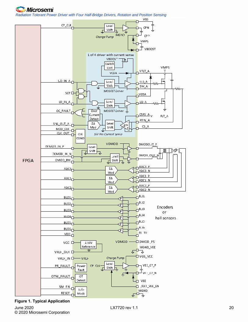
Figure 1. Typical Application
Introduction to the LX7720
June 2020 LX7720 rev 1.1 21 © 2020 Microsemi Corporation
12 Introduction to the LX7720 The LX7720 targets motors that can be managed by 4 independent low-side FET drivers and 4 independent high-side FET drivers, with PWM control up to 40kHz. Typical motor applications include: • A 3-phase star-connected Permanent Magnet Synchronous Motor (PMSM) or Brushless DC Motor (BLDC)
Each of the 3 motor phase windings is driven by a half-bridge The 4th half-bridge drive is available for an electromagnetic brake
• A 2-winding bipolar stepper motor, operated in full-step, half-step, or micro-stepping mode Each winding is driven by an H-bridge comprising a half-bridge at each side of the winding
Position feedback options built in to the LX7720 allow any combination of the interfaces below: • One or more optical encoder using the 6 built in BLI/BLO comparators • Up to six Hall effect sensors using some of the 6 built in BLI/BLO comparators • An LVDT, RVDT, or resolver using the built-in primary driver and dual ADCs for the two secondaries FPGAs are traditionally used as the system controller for space motor drives, and user guides for Microsemi provided FPGA IP can be found here: https://www.microsemi.com/applications/motor-control#ip-suite. Further information is also available at https://www.microsemi.com/applications/motor-control#resources. Higher end microcontrollers with embedded PWM peripherals are also capable of managing the LX7720. For example, the radiation-hardened SAMRH71F20 and the radiation-tolerant SAMV71Q21RT ARM-based MCUs include two 16-bit PWM blocks. Each PWM block provides 4 complementary outputs with dead-time control, enough to control up to 4 half-bridges driving a motor. One of these MCUs can therefore manage two independent motor-driving LX7720s. The LX7720 Daughter Board User Guide also contains useful information supplementary to this data sheet.
13 Power Supplies, Sequencing, and Voltage Reference 13.1 Power Supply Configurations and Decoupling The LX7720 requires several supply voltages (Table 1) and generates floating high-side gate drive rails for the external half-bridges. A negative supply rail, VEE, is generated by an internal charge pump or supplied externally (Table 2). Table 1. Power Supplies and Recommended Decoupling Capacitors
Supply Pin Voltage Range Notes Capacitor Ground VMPS 20V to 60V Motor supply, as reference for the upper MOSFET drivers 1µF MGND VCC 4.75V to 5.25V Main circuitry positive power supply 3x 1µF SGND VDD 2.1V to 5.5V External FPGA or MCU controller's I/O power supply 1µF SGND VEE -VGS to -8V Main circuitry negative power supply 2.2µF MGND
DMOD_PS 10V to 18V Resolver or LVDT power supply 10µF SGND VREF_OUT 2.5V Internal voltage reference 0.47µF SGND
VGS, VGS_A, VGS_B, VGS_C, VGS_D 10V to 18V FET gate drive rail. Use 1µF on the VGS pins, and 10µF
on the VGS_A, VGS_B, VGS_C, and VGS_D pins 2x 1µF, and
4x 10µF MGND
VFLT_A, VFLT_B, VFLT_C, VFLT_D VMPS + VGS Floating gate driver power rails 4x 1µF SW_#
CS_A, CS_B, CS_C, CS_D VFLT_# or VGS Floating or low-side current sense power rails 4x 1µF RTN_#
13.2 VEE Options The negative signal supply, VEE, is generated by default by an internal charge pump operating from VGS. The charge pump can be disabled to allow an external -VGS to -8V supply to be used instead (Table 2). Table 2. VEE Supply Methods
VEE Supply Method EXT_VEE_EN pin
Capacitor Between VEE_CP_P pin and VEE_CP_N pin
Capacitor on VEE pin
VEE internally generated by inverting charge pump from VGS Open or VGS 1µF
VEE externally supplied (-VGS to -8V) directly to VEE pin SGND Not fitted. Leave VEE_CP_P and VEE_CP_N pins open
2.2µF to MGND
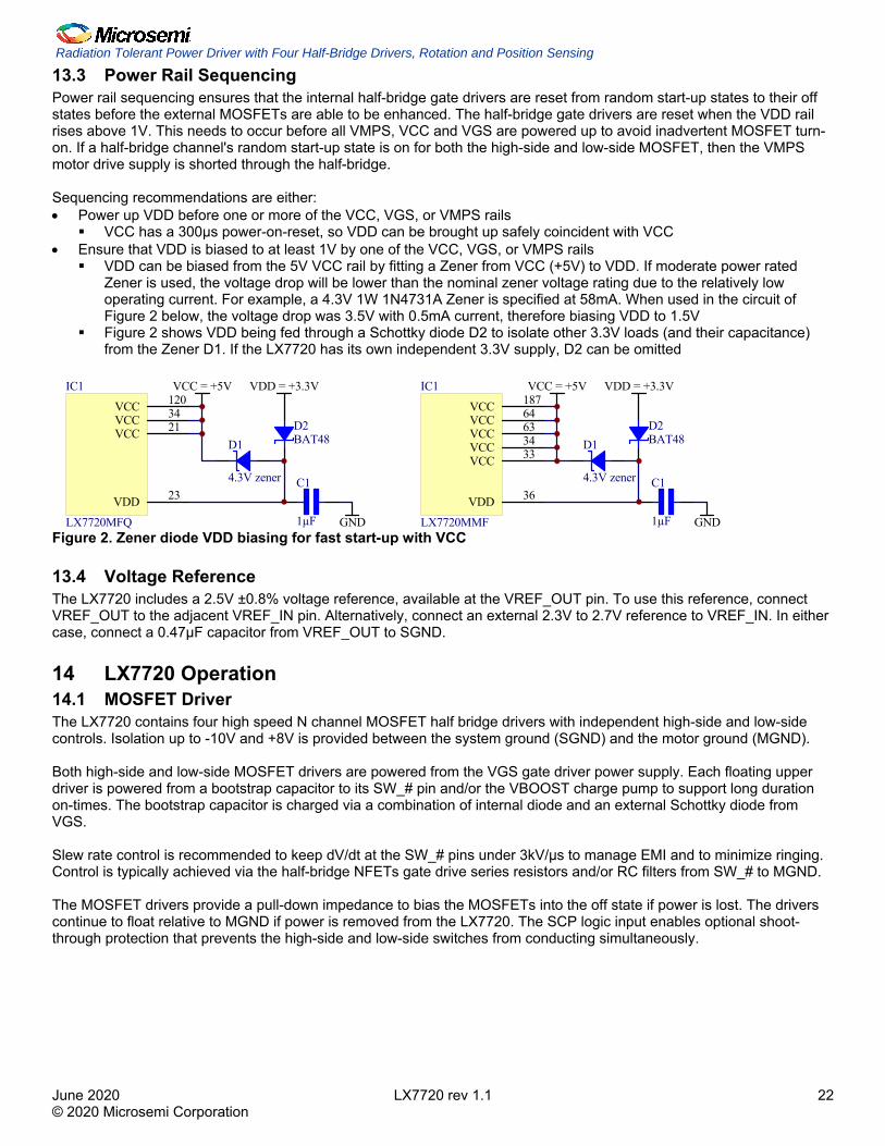
Radiation Tolerant Power Driver with Four Half-Bridge Drivers, Rotation and Position Sensing
June 2020 LX7720 rev 1.1 22 © 2020 Microsemi Corporation
13.3 Power Rail Sequencing Power rail sequencing ensures that the internal half-bridge gate drivers are reset from random start-up states to their off states before the external MOSFETs are able to be enhanced. The half-bridge gate drivers are reset when the VDD rail rises above 1V. This needs to occur before all VMPS, VCC and VGS are powered up to avoid inadvertent MOSFET turn-on. If a half-bridge channel's random start-up state is on for both the high-side and low-side MOSFET, then the VMPS motor drive supply is shorted through the half-bridge. Sequencing recommendations are either: • Power up VDD before one or more of the VCC, VGS, or VMPS rails
VCC has a 300µs power-on-reset, so VDD can be brought up safely coincident with VCC • Ensure that VDD is biased to at least 1V by one of the VCC, VGS, or VMPS rails
VDD can be biased from the 5V VCC rail by fitting a Zener from VCC (+5V) to VDD. If moderate power rated Zener is used, the voltage drop will be lower than the nominal zener voltage rating due to the relatively low operating current. For example, a 4.3V 1W 1N4731A Zener is specified at 58mA. When used in the circuit of Figure 2 below, the voltage drop was 3.5V with 0.5mA current, therefore biasing VDD to 1.5V
Figure 2 shows VDD being fed through a Schottky diode D2 to isolate other 3.3V loads (and their capacitance) from the Zener D1. If the LX7720 has its own independent 3.3V supply, D2 can be omitted
GND
C1
1µF
.
D1
4.3V zener
GND
D2BAT48
C1
1µF
VDD = +3.3VVCC = +5V
.
VCC 21
VCC 120
VDD 23
VCC 34
IC1
LX7720MFQ
VCC 33
VCC 187
VDD 36
VCC 34
VCC 64
VCC 63
IC1
LX7720MMF
D1
4.3V zener
D2BAT48
VDD = +3.3VVCC = +5V
Figure 2. Zener diode VDD biasing for fast start-up with VCC
13.4 Voltage Reference The LX7720 includes a 2.5V ±0.8% voltage reference, available at the VREF_OUT pin. To use this reference, connect VREF_OUT to the adjacent VREF_IN pin. Alternatively, connect an external 2.3V to 2.7V reference to VREF_IN. In either case, connect a 0.47µF capacitor from VREF_OUT to SGND.
14 LX7720 Operation 14.1 MOSFET Driver The LX7720 contains four high speed N channel MOSFET half bridge drivers with independent high-side and low-side controls. Isolation up to -10V and +8V is provided between the system ground (SGND) and the motor ground (MGND). Both high-side and low-side MOSFET drivers are powered from the VGS gate driver power supply. Each floating upper driver is powered from a bootstrap capacitor to its SW_# pin and/or the VBOOST charge pump to support long duration on-times. The bootstrap capacitor is charged via a combination of internal diode and an external Schottky diode from VGS. Slew rate control is recommended to keep dV/dt at the SW_# pins under 3kV/µs to manage EMI and to minimize ringing. Control is typically achieved via the half-bridge NFETs gate drive series resistors and/or RC filters from SW_# to MGND. The MOSFET drivers provide a pull-down impedance to bias the MOSFETs into the off state if power is lost. The drivers continue to float relative to MGND if power is removed from the LX7720. The SCP logic input enables optional shoot-through protection that prevents the high-side and low-side switches from conducting simultaneously.

LX7720 Operation
June 2020 LX7720 rev 1.1 23 © 2020 Microsemi Corporation
14.2 Floating Current Sense Each MOSFET driver offers a floating current sense circuit that can be referenced to either MGND (low-side measurement) or to the driver's SW_# pin (high-side measurement). The current sense inputs accept voltages up to ±200mV to measure either MGND return current or SW_ motor winding current. The sensed voltage is amplified and level shifted to an SGND referenced 2nd order sigma delta modulator using the sample clock MOD_CLK and with internal sampling synchronized to CLK_OUT. The CS_# voltage relative to RTN_# of 0V is converted to a 50% full scale output. Positive amplitudes (current flow from CS_# to RTN_#) register as >50% of full scale and negative differential amplitudes register as <50% of full scale. The resultant bit stream is sent to the FPGA/MCU controller to be processed using a sinc3 filter and decimator. A decimation ratio (OSR) of 16 provides almost 9 bits of accuracy with a filter response time of 5µs with a 32MHz sample rate. If high-side current measurement is used, it is recommended to apply a median filter to the output of the current sense sinc3 filter (Figure 3) before the data is used by the motor control algorithm. The median filter rejects artifacts in the current sense Σ-Δ modulator output pulse train due to transitions at the SW_# pin. An n order median filter is a rolling or sliding window filter which examines the most recent n samples, sorts them, and outputs the value of the median sample.
OSR Median Order n 16 13 32 9 64 7 128 5 256 3
Figure 3. Median Filter Recommendation A modulator will enter sleep mode after both UD_IN_# and LD_IN_# are simultaneously de-asserted for more than 8192 MOD_CLK cycles. The floating current sense is powered from its CSPS_# pin. The current sense continues to float relative to MGND when power to the LX7720 is removed.
14.3 Fixed Bi-Level Comparators Inputs and Outputs - Hall Effect Sensors and Encoders The bi-level comparators comprise 6 comparators with non-inverting inputs at pins BLI1 to BLI6, and logic outputs at pins BLO1 to BLO6. The 6 inverting inputs share a common rising-input trip threshold at the BL_TH pin. Bias BL_TH between 0.5V and 4.5V. The hysteresis is typically 150mV on falling edges. Low pass input filters and threshold hysteresis provides high frequency noise rejection. The bi-level inputs are cold spared.
14.4 FPGA/MCU Controller Interface I/O logic levels are set by the voltage at the VDD logic supply pin, in the range 2.1V to 5.5V. Logic input pins have an internal 1MΩ pull down resistor to ground.
14.5 Over-Current Detection The current sense detection circuitry detects when a driven winding current exceeds typically ±320mV across the current sense resistor, and latches the OC_FAULT logic output. A low pass filter prevents very short duration spikes (under typically 15µs) from triggering over-current detection.
14.6 Power Faults and Driver Overload The MOSFET drivers and DMOD_OUT_# drivers latch the PR_FAULT logic output if an average drive current level exceed the over-current thresholds. The VGS current is monitored for all the MOSFET drivers. The DMOD_PS current is monitored for the resolver demodulator driver. PR_FAULT is also latched if the monitored voltage rails fall below the UVLO threshold levels specified in the Electrical Characteristics table.
Radiation Tolerant Power Driver with Four Half-Bridge Drivers, Rotation and Position Sensing
June 2020 LX7720 rev 1.1 24 © 2020 Microsemi Corporation
14.7 Over-temperature Warning If the die temperature exceeds the over temperature warning threshold, the OTW_FAULT logic output will be asserted. This warning allows a small operating window before the die temperature reaches the over-temperature shutdown threshold. The over-temperature shutdown is a latched fault state when safe mode is enabled.
14.8 RESET and SAFE MODE Once a fault is latched, it can be reset by clearing the fault condition and then either toggling RESET pin 18 or cycling the power. Safe mode is enabled by leaving the SM_EN logic input either open or tied to VDD. Safe mode is armed after power up by the power on reset and UVLO de-assertions. When enabled, the LX7720 exerts counter measures whenever a fault is latched: • If an OC_FAULT is detected, the LX7720 will place all external MOSFET switches in the off state • If a PR_FAULT is detected, the LX7720 will place all external MOSFET switches in the off state and place both
DMOD_OUT_P and DMOD_OUT_N in the low state • If the over-temperature shut down threshold is exceeded and latched or if MOD_CLK is stopped, the LX7720 enters a
low power state except for the FPGA control lines and the RESET function circuitry. All external MOSFETs default to the off state in low power mode. The MOD_CLK stopped fault is not a latched fault; operation resumes when MOD_CLK is restored
If safe mode is not enabled, the LX7720 will rely exclusively on the system FPGA or MCU to manage fault mitigation such as shutting off the external MOSFETs or disconnecting a power rail.
14.9 Resolver/LVDT to Digital Interface The resolver interface consists of a differential driver output DMOD_OUT_P and DMOD_OUT_N to drive a resolver or LVDT's primary, plus three differential acquisition inputs ADC1, ADC2, and ADC3. ADC1 and ADC2 are typically used to sense the two secondary output voltages. ADC3 is typically used to sense the primary voltage. If the DMOD_IN_N and DMOD_IN_P inputs remain low for more than 65536 MOD_CLK cycles, the DMOD_OUT_N and DMOD_OUT_P outputs both become a high impedance. The resolver primary is typically driven with a sinusoidal carrier voltage with a frequency that ranges from 360Hz to 20kHz. The DMOD_OUT_P and DMOD_OUT_N differential outputs are driven with a pulse width modulated signal from DEMOD_IN_P and DEMOD_IN_N respectively. The differential output can be filtered similar to a class-D audio signal. The DMOD_OUT_P and DMOD_OUT_N output drivers are powered from a separate higher voltage rail (DMOD_PS) so they can provide a wide dynamic range; the DMOD_PS rail is referenced to the MGND. The driver bias current can be reduced by grounding the DMOD_BW input, which also reduces the maximum pulse rate of the driver. The ADC1, ADC2, and ADC3 differential inputs are referenced to VREF, and may require an external attenuation voltage divider to be compatible with the voltage range of these inputs (SGND to VCC). A differential input voltage of 0V is converted to a 50% full scale output. Positive amplitudes are registered as >50% of full scale, and negative differential amplitudes are registered as <50% of full scale. The 2nd order sigma delta modulator samples at the MOD_CLK rate or a sample range of 24 MHz to 32 MHz. The resultant bit stream is sent to the FPGA to be processed using a sinc3 filter and decimator. A decimation ratio of 64 to 256 provides accuracies from 10 to 14 bits. The sample rate is set by MOD_CLK and sampling is synchronized to CLK_OUT. A modulator will enter sleep mode after both ADC#_P and ADC#_N are simultaneously held to VCC for more than 8192 MOD_CLK cycles.
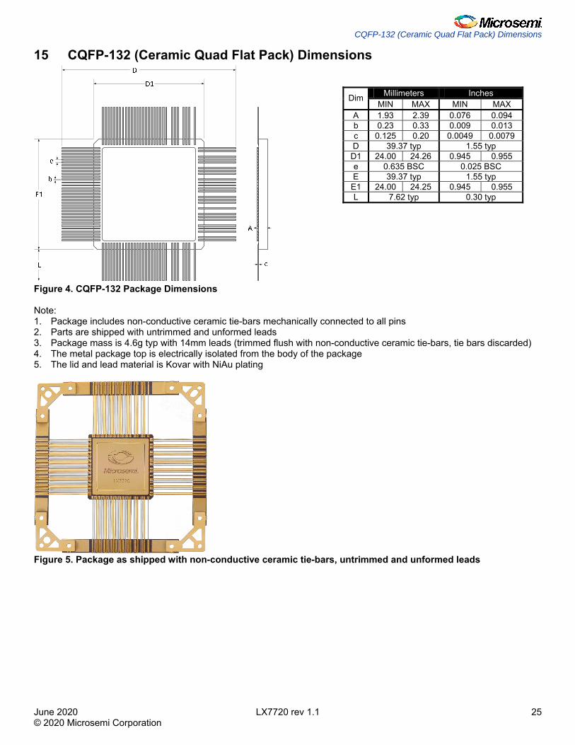
CQFP-132 (Ceramic Quad Flat Pack) Dimensions
June 2020 LX7720 rev 1.1 25 © 2020 Microsemi Corporation
15 CQFP-132 (Ceramic Quad Flat Pack) Dimensions
Figure 4. CQFP-132 Package Dimensions
Millimeters Inches DimMIN MAX MIN MAX
A 1.93 2.39 0.076 0.094 b 0.23 0.33 0.009 0.013 c 0.125 0.20 0.0049 0.0079 D 39.37 typ 1.55 typ D1 24.00 24.26 0.945 0.955 e 0.635 BSC 0.025 BSC E 39.37 typ 1.55 typ E1 24.00 24.25 0.945 0.955 L 7.62 typ 0.30 typ
Note: 1. Package includes non-conductive ceramic tie-bars mechanically connected to all pins 2. Parts are shipped with untrimmed and unformed leads 3. Package mass is 4.6g typ with 14mm leads (trimmed flush with non-conductive ceramic tie-bars, tie bars discarded) 4. The metal package top is electrically isolated from the body of the package 5. The lid and lead material is Kovar with NiAu plating
Figure 5. Package as shipped with non-conductive ceramic tie-bars, untrimmed and unformed leads
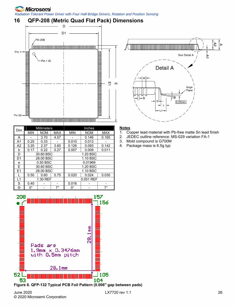
Radiation Tolerant Power Driver with Four Half-Bridge Drivers, Rotation and Position Sensing
June 2020 LX7720 rev 1.1 26 © 2020 Microsemi Corporation
16 QFP-208 (Metric Quad Flat Pack) Dimensions
Millimeters Inches Dim
MIN NOM MAX MIN NOM MAX A - 3.70 4.07 - 0.146 0.160 A1 0.25 0.33 - 0.010 0.013 - A2 3.20 2.37 3.60 0.126 0.093 0.142 b 0.17 0.22 0.27 0.007 0.009 0.011 D 30.60 BSC 1.20 BSC D1 28.00 BSC 1.10 BSC e 0.50 BSC 0.01969 E 30.60 BSC 1.20 BSC E1 28.00 BSC 1.10 BSC L 0.50 0.60 0.75 0.020 0.024 0.030
L1 1.30 REF 0.051 REF S 0.40 - - 0.016 - - Θ 0° - 7° 0° - 7°
Notes 1. Copper lead material with Pb-free matte Sn lead finish 2. JEDEC outline reference: MS-029 variation FA-1 3. Mold compound is G700M 4. Package mass is 6.5g typ
Figure 6. QFP-132 Typical PCB Foil Pattern (0.006" gap between pads)
Change Log
June 2020 LX7720 rev 1.1 27 © 2020 Microsemi Corporation
17 Change Log Date Issue Part Type
2019-11-20 1.0 First release
2020-6-17 1.1
Added plastic package. Noted that CQFP-132 ES part is not hermetic, lid and lead material is Kovar, lid is isolated, θJB = 1.93°C/W from package back. Added CDM ESD, moved ESD ratings to separate section. Updated ceramic pinout drawing to show ground planes and decoupling. Shipping type updated to tray in order table. Added introduction section. Added power supply section including sequencing recommendations. Section 11 text cleanup for clarity. Corrected omitted package pins in Figure 2 and Figure 3. Corrected pin descriptions: VGS pins mislabeled ground instead of power, diodes go to VGS_# not SW_#, swapped pin 91/92 and pins 103/104 text, VFLT_# capacitors go to SW_# not MGND, VBOOST capacitor goes to VMPS not MGND, CPP swing, VEE_CP_N swing. Added description for SPARE pin 53. Corrected pin reference numbers in description for pins 11, 12, 44, 46. Added gate drive resistor value to pin descriptions. Added gate drive resistors to block diagram. Updated EC table to show that OTW_FAULT output can not be tested at +125°C. -2V pin renamed TESTMODE0. Clarified krad to krad(Si), added SAM3X8ERT to first page
Microsemi Corporation (Nasdaq: MSCC) offers a comprehensive portfolio of semiconductor and system solutions for communications, defense & security, aerospace and industrial markets. Products include high-performance and radiation-hardened analog mixed-signal integrated circuits, FPGAs, SoCs and ASICs; power management products; timing and synchronization devices and precise time solutions, setting the world’s standard for time; voice processing devices; RF solutions; discrete components; security technologies and scalable anti-tamper products; Power-over-Ethernet ICs and midspans; as well as custom design capabilities and services. Microsemi is headquartered in Aliso Viejo, Calif., and has approximately 3,400 employees globally. Learn more at www.microsemi.com.
Microsemi makes no warranty, representation, or guarantee regarding the information contained herein or the suitability of its products and services for any particular purpose, nor does Microsemi assume any liability whatsoever arising out of the application or use of any product or circuit. The products sold hereunder and any other products sold by Microsemi have been subject to limited testing and should not be used in conjunction with mission-critical equipment or applications. Any performance specifications are believed to be reliable but are not verified, and Buyer must conduct and complete all performance and other testing of the products, alone and together with, or installed in, any end-products. Buyer shall not rely on any data and performance specifications or parameters provided by Microsemi. It is the Buyer’s responsibility to independently determine suitability of any products and to test and verify the same. The information provided by Microsemi hereunder is provided “as is, where is” and with all faults, and the entire risk associated with such information is entirely with the Buyer. Microsemi does not grant, explicitly or implicitly, to any party any patent rights, licenses, or any other IP rights, whether with regard to such information itself or anything described by such information. Information provided in this document is proprietary to Microsemi, and Microsemi reserves the right to make any changes to the information in this document or to any products and services at any time without notice.
Microsemi Corporate Headquarters One Enterprise, Aliso Viejo, CA 92656 USA Within the USA: +1 (800) 713-4113 Outside the USA: +1 (949) 380-6100 Sales: +1 (949) 380-6136 Fax: +1 (949) 215-4996 E-mail: [email protected]
© 2020 Microsemi Corporation. All rights reserved. Microsemi and the Microsemi logo are trademarks of Microsemi Corporation. All other trademarks and service marks are the property of their respective owners.