Embed Size (px)
Citation preview
General DescriptionDARWIN is a new breed of low-power microcontrollers built to thrive in the rapidly evolving Internet of Things (IoT). They are smart, with the biggest memories in their class and a massively scalable memory architecture. They run forever, thanks to wearable-grade power technology. They are also tough enough to withstand the most advanced cyberattacks. DARWIN microcontrollers are designed to run any application imaginable—in places where you wouldn’t dream of sending other microcontrollers.Generation U microcontrollers are perfect for wearables and IoT applications that cannot afford to compromise power or performance. The MAX32630–MAX32632 fea-ture an Arm® Cortex®-M4 with FPU CPU that delivers ultra-low power, high-efficiency signal processing func-tionality with significantly reduced power consumption and ease of use.Flexible power modes, an intelligent peripheral management unit (PMU), dynamic clock gating and firmware-controlled power gating optimizes power for the specific application.Multiple SPI, UART, I2C, 1-Wire® master, and USB inter-faces are provided. The four-input, 10-bit ADC with select-able references can monitor external sensors.The MAX32631/MAX32632 are secure versions of the MAX32630. They provide a trust protection unit (TPU) with encryption and advanced security features. These include a modular arithmetic accelerator (MAA) for fast ECDSA, a true random number generator, and a hardware AES engine. The MAX32632 also provides a secure bootloader for additional security and life-cycle management.
Applications ● Sports Watches ● Fitness Monitors ● Wearable Medical Patches ● Portable Medical Devices ● Sensor Hubs
Benefits and Features ● High-Efficiency Microcontroller for Wearable Devices
• Internal Oscillator Operates Up to 96MHz• Low Power 4MHz Oscillator System Clock Option
for Always-On Monitoring Applications• 2MB Flash Memory• 512KB SRAM• 8KB Instruction Cache• 1.2V CPU Core Supply Voltage• 1.8V to 3.3V I/O• Optional 3.3V ±5% USB Supply Voltage
● Power Management Maximizes Uptime for Battery Applications• 106μA/MHz Active Current Executing from Cache• Wakeup to 96MHz Clock or 4MHz Clock• 600nA Low Power Mode (LP0) Current with RTC
Enabled• 3.5μW/MHz Ultra-Low Power Data Retention Sleep
Mode (LP1) with Fast 5μs Wakeup to 96MHz ● Optimal Peripheral Mix Provides Platform Scalability
• SPIX Execute in Place (XIP) Engine for Memory Expansion with Minimal Footprint
• Up to Three SPI Masters, One SPI Slave• Four UARTs• Up to Three I2C Masters, One I2C Slave• 1-Wire Master• Full-Speed USB 2.0 Engine with Internal
Transceiver• Sixteen Pulse Train (PWM) Engines• Six 32-Bit Timers and 3 Watchdog Timers• Up to 66 General-Purpose I/O Pins• One 10-Bit Delta-Sigma ADC Operating at 7.8ksps• RTC Calibration Output
● Secure Valuable IP and Data with Robust Internal Hardware Security (MAX32631 and MAX32632 Only)• Trust Protection Unit (TPU) Including MAA
Supports ECDSA and Modular Arithmetic• True Random Number Generator• AES-128, -192, -256• Secure Bootloader (MAX32632 Only)Ordering Information appears at end of data sheet.
Arm and Cortex are registered trademarks of Arm Limited (or its subsidiaries) in the US and/or elsewhere.1-Wire is a registered trademark of Maxim Integrated Products, Inc.
19-8478; Rev 5; 10/18
MAX32630–MAX32632 Ultra-Low-Power Arm Cortex-M4 with FPU-Based Microcontroller (MCU)
with 2MB Flash and 512KB SRAM
EVALUATION KIT AVAILABLE
Simplified Block Diagram
MAX32630–MAX32632
BUS
MATR
IX –
AHB,
APB
, IBUS
, DBU
S…
ARM CORTEX-M4 96MHz
NVIC
JTAG SWD (SERIAL WIRE DEBUG)
POR,BROWNOUT MONITOR,
SUPPLY VOLTAGE MONITORS
VOLTAGE REGULATION &
POWER CONTROL
CLOCK GENERATION
96MHz INT OSC/SYSTEM CLOCK
USB 2.0 FULL SPEED
CONTROLLER
MEMORY
2MB FLASH
512KB SRAM
8KB CACHE
PERIPHERAL MANAGEMENT UNIT
3 × WINDOWED WATCHDOG TIMERS
CRC 16/32
RTC & WAKE-UP TIMERS
TRUST PROTECTION UNIT (TPU)MAX32631 AND MAX32632
10-BIT ΣΔ ADC
AIN0AIN1AIN2AIN3
VDDB
VRTC
TCK/SWCLKTMS/SWDIO
TDOTDI
RSTN
SRSTN
VDD12VDD18VRTC
VSS
32KOUT32KIN
DPDM
VDDB
UP TO 66 GPIO/SPECIAL FUNCTION
GPIO WITH INTERRUPTS
SECURE NV KEY
UNIQUE ID
TRNG
SECURE BOOTLOADER(MAX32630 ONLY)
÷5÷5
÷4
VDD12÷2
6 × 32 BIT TIMERS
16 × PULSE TRAIN ENGINE
3 × SPI MASTER32
B FI
FOS
1 × SPI XIP
3 × I2C MASTER 1 × I2C SLAVEMaximum of 3
Ports16B
FIFO
S
4 × UART32B
FIFO
S
1-WIRE MASTER
1 × SPI SLAVE
VDD18
VDDIOH
SHARED PAD FUNCTIONS
TIMERS/PWMCAPTURE/COMPARE
USBSPI
SPI XIPI2C
UART1-WIRE
RTC OUTPUT
EXTERNAL INTERRUPTS
VDDIO
VDDAVSSA
VREF
EXT REF1.2V
MAAAES-128, -192, -256
www.maximintegrated.com Maxim Integrated │ 2
MAX32630–MAX32632 Ultra-Low-Power Arm Cortex-M4 with FPU-Based Microcontroller (MCU)
with 2MB Flash and 512KB SRAM
(All voltages with respect to VSS, unless otherwise noted.)VDD18 .................................................................-0.3V to +1.89VVDD12 .................................................................-0.3V to +1.26VVDDA relative to VSSA ........................................-0.3V to +1.89VVRTC ...................................................................-0.3V to +1.89VVDDB ....................................................................-0.3V to +3.6VVREF .....................................................................-0.3V to +3.6V32KIN, 32KOUT....................................................-0.3V to +3.6VRSTN, SRSTN, DP, DM, GPIO, JTAG .................-0.3V to +3.6VAIN[1:0].................................................................-0.3V to +5.5VAIN[3:2].................................................................-0.3V to +3.6V
VDDIO ...................................................................-0.3V to +3.6VVDDIOH .................................................................-0.3V to +3.6VTotal Current into All VDD18 Power Pins (sink) ................100mATotal Current into VSS ......................................................100mAOutput Current (sink) by Any I/O Pin..................................25mAOutput Current (source) by Any I/O Pin ............................-25mAContinuous Package Power Dissipation TQFP (multilayer board)
TA = +70°C (derate 45.5mW/°C above +70°C) ......3636.4mWOperating Temperature Range ........................... -20°C to +85°CStorage Temperature Range ............................ -65°C to +150°CSoldering Temperature (reflow) .......................................+260°C
100 WLPPackage Code W1004D4+1Outline Number 21-100043Land Pattern Number Refer to Application Note 1891Thermal Resistance, Single-Layer BoardJunction-to-Ambient (θJA) N/AJunction-to-Case Thermal Resistance (θJC) N/AThermal Resistance, Four-Layer BoardJunction-to-Ambient (θJA) 38.9°C/WJunction-to-Case Thermal Resistance (θJC) N/A
100 TQFP-EPPackage Code C100E+3Outline Number 21-0116Land Pattern Number Refer to Application Note 1891Thermal Resistance, Single-Layer BoardJunction-to-Ambient (θJA) N/AJunction-to-Case Thermal Resistance (θJC) N/AThermal Resistance, Four-Layer BoardJunction-to-Ambient (θJA) 22°C/WJunction-to-Case Thermal Resistance (θJC) 2°C/W
Package thermal resistances were obtained using the method described in JEDEC specification JESD51-7, using a four-layer board. For detailed information on package thermal considerations, refer to www.maximintegrated.com/thermal-tutorial.
Absolute Maximum Ratings
Stresses beyond those listed under “Absolute Maximum Ratings” may cause permanent damage to the device. These are stress ratings only, and functional operation of the device at these or any other conditions beyond those indicated in the operational sections of the specifications is not implied. Exposure to absolute maximum rating conditions for extended periods may affect device reliability.
For the latest package outline information and land patterns (footprints), go to www.maximintegrated.com/packages. Note that a “+”, “#”, or “-” in the package code indicates RoHS status only. Package drawings may show a different suffix character, but the drawing pertains to the package regardless of RoHS status.
Package Information
www.maximintegrated.com Maxim Integrated │ 3
MAX32630–MAX32632 Ultra-Low-Power Arm Cortex-M4 with FPU-Based Microcontroller (MCU)
with 2MB Flash and 512KB SRAM
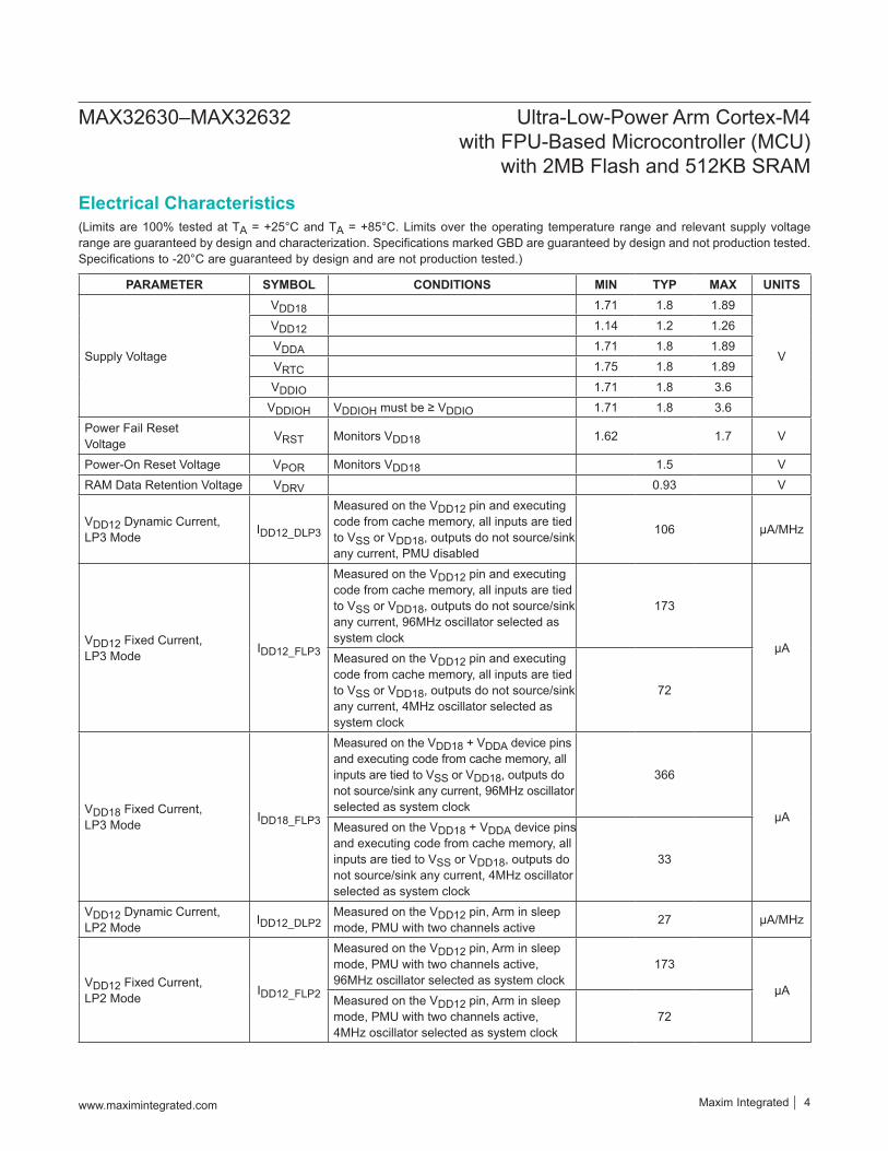
(Limits are 100% tested at TA = +25°C and TA = +85°C. Limits over the operating temperature range and relevant supply voltage range are guaranteed by design and characterization. Specifications marked GBD are guaranteed by design and not production tested. Specifications to -20°C are guaranteed by design and are not production tested.)
PARAMETER SYMBOL CONDITIONS MIN TYP MAX UNITS
Supply Voltage
VDD18 1.71 1.8 1.89
V
VDD12 1.14 1.2 1.26VDDA 1.71 1.8 1.89VRTC 1.75 1.8 1.89VDDIO 1.71 1.8 3.6
VDDIOH VDDIOH must be ≥ VDDIO 1.71 1.8 3.6Power Fail Reset Voltage VRST Monitors VDD18 1.62 1.7 V
Power-On Reset Voltage VPOR Monitors VDD18 1.5 V RAM Data Retention Voltage VDRV 0.93 V
VDD12 Dynamic Current, LP3 Mode IDD12_DLP3
Measured on the VDD12 pin and executing code from cache memory, all inputs are tied to VSS or VDD18, outputs do not source/sink any current, PMU disabled
106 μA/MHz
VDD12 Fixed Current, LP3 Mode IDD12_FLP3
Measured on the VDD12 pin and executing code from cache memory, all inputs are tied to VSS or VDD18, outputs do not source/sink any current, 96MHz oscillator selected as system clock
173
μA Measured on the VDD12 pin and executing code from cache memory, all inputs are tied to VSS or VDD18, outputs do not source/sink any current, 4MHz oscillator selected as system clock
72
VDD18 Fixed Current, LP3 Mode IDD18_FLP3
Measured on the VDD18 + VDDA device pins and executing code from cache memory, all inputs are tied to VSS or VDD18, outputs do not source/sink any current, 96MHz oscillator selected as system clock
366
μA Measured on the VDD18 + VDDA device pins and executing code from cache memory, all inputs are tied to VSS or VDD18, outputs do not source/sink any current, 4MHz oscillator selected as system clock
33
VDD12 Dynamic Current, LP2 Mode IDD12_DLP2
Measured on the VDD12 pin, Arm in sleep mode, PMU with two channels active 27 μA/MHz
VDD12 Fixed Current, LP2 Mode IDD12_FLP2
Measured on the VDD12 pin, Arm in sleep mode, PMU with two channels active, 96MHz oscillator selected as system clock
173
μA Measured on the VDD12 pin, Arm in sleep mode, PMU with two channels active, 4MHz oscillator selected as system clock
72
Electrical Characteristics
www.maximintegrated.com Maxim Integrated │ 4
MAX32630–MAX32632 Ultra-Low-Power Arm Cortex-M4 with FPU-Based Microcontroller (MCU)
with 2MB Flash and 512KB SRAM
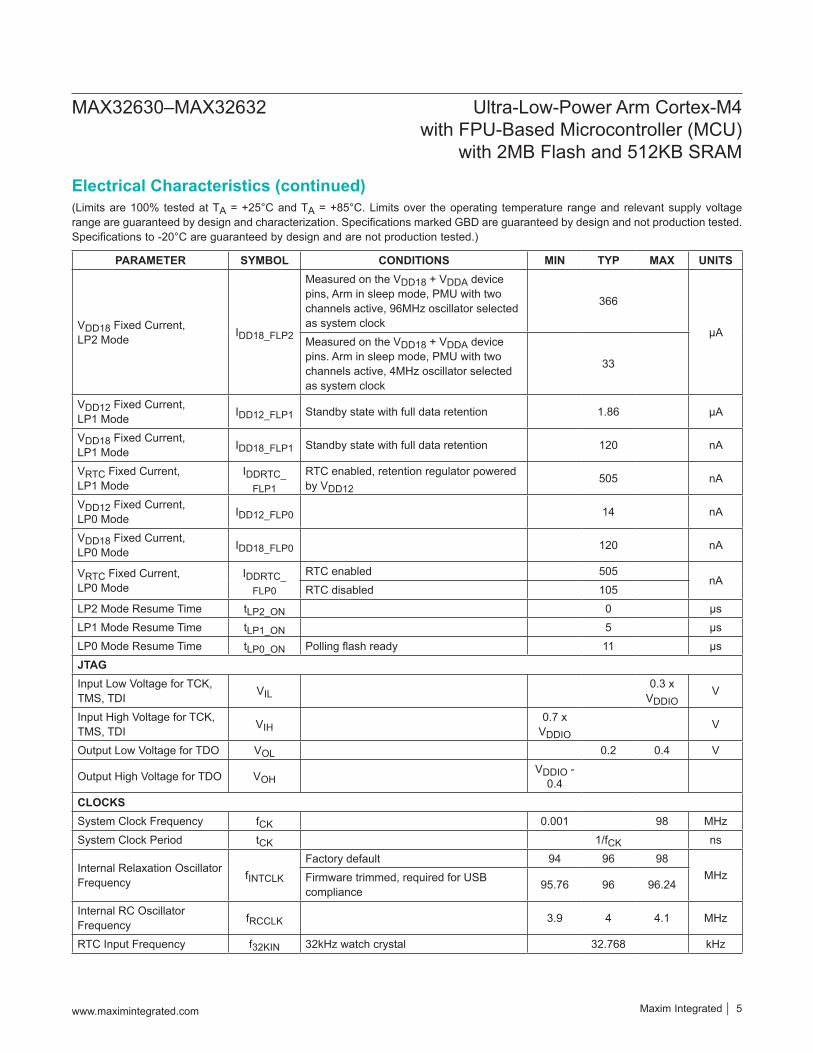
(Limits are 100% tested at TA = +25°C and TA = +85°C. Limits over the operating temperature range and relevant supply voltage range are guaranteed by design and characterization. Specifications marked GBD are guaranteed by design and not production tested. Specifications to -20°C are guaranteed by design and are not production tested.)
PARAMETER SYMBOL CONDITIONS MIN TYP MAX UNITS
VDD18 Fixed Current, LP2 Mode IDD18_FLP2
Measured on the VDD18 + VDDA device pins, Arm in sleep mode, PMU with two channels active, 96MHz oscillator selected as system clock
366
μA Measured on the VDD18 + VDDA device pins. Arm in sleep mode, PMU with two channels active, 4MHz oscillator selected as system clock
33
VDD12 Fixed Current, LP1 Mode IDD12_FLP1 Standby state with full data retention 1.86 μA
VDD18 Fixed Current, LP1 Mode IDD18_FLP1 Standby state with full data retention 120 nA
VRTC Fixed Current, LP1 Mode
IDDRTC_FLP1
RTC enabled, retention regulator powered by VDD12
505 nA
VDD12 Fixed Current, LP0 Mode IDD12_FLP0 14 nA
VDD18 Fixed Current, LP0 Mode IDD18_FLP0 120 nA
VRTC Fixed Current, LP0 Mode
IDDRTC_FLP0
RTC enabled 505nA
RTC disabled 105LP2 Mode Resume Time tLP2_ON 0 μs LP1 Mode Resume Time tLP1_ON 5 μs LP0 Mode Resume Time tLP0_ON Polling flash ready 11 μs JTAGInput Low Voltage for TCK, TMS, TDI VIL
0.3 x VDDIO
V
Input High Voltage for TCK, TMS, TDI VIH
0.7 x VDDIO
V
Output Low Voltage for TDO VOL 0.2 0.4 V
Output High Voltage for TDO VOHVDDIO -
0.4CLOCKSSystem Clock Frequency fCK 0.001 98 MHz System Clock Period tCK 1/fCK ns
Internal Relaxation Oscillator Frequency fINTCLK
Factory default 94 96 98MHz Firmware trimmed, required for USB
compliance 95.76 96 96.24
Internal RC Oscillator Frequency fRCCLK 3.9 4 4.1 MHz
RTC Input Frequency f32KIN 32kHz watch crystal 32.768 kHz
Electrical Characteristics (continued)
www.maximintegrated.com Maxim Integrated │ 5
MAX32630–MAX32632 Ultra-Low-Power Arm Cortex-M4 with FPU-Based Microcontroller (MCU)
with 2MB Flash and 512KB SRAM
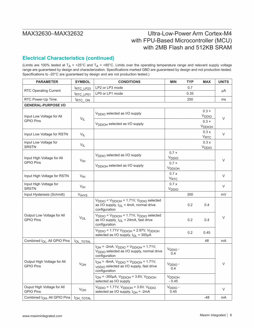
(Limits are 100% tested at TA = +25°C and TA = +85°C. Limits over the operating temperature range and relevant supply voltage range are guaranteed by design and characterization. Specifications marked GBD are guaranteed by design and not production tested. Specifications to -20°C are guaranteed by design and are not production tested.)
PARAMETER SYMBOL CONDITIONS MIN TYP MAX UNITS
RTC Operating Current IRTC_LP23 LP2 or LP3 mode 0.7
μA IRTC_LP01 LP0 or LP1 mode 0.35
RTC Power-Up Time tRTC_ ON 250 ms GENERAL-PURPOSE I/O
Input Low Voltage for All GPIO Pins VIL
VDDIO selected as I/O supply 0.3 × VDDIO V
VDDIOH selected as I/O supply 0.3 × VDDIOH
Input Low Voltage for RSTN VIL0.3 x VRTC
V
Input Low Voltage for SRSTN VIL
0.3 x VDDIO
Input High Voltage for All GPIO Pins VIH
VDDIO selected as I/O supply 0.7 × VDDIO V
VDDIOH selected as I/O supply 0.7 × VDDIOH
Input High Voltage for RSTN VIH0.7 x VRTC
V
Input High Voltage for SRSTN VIH
0.7 x VDDIO
V
Input Hysteresis (Schmitt) VIHYS 300 mV
Output Low Voltage for All GPIO Pins VOL
VDDIO = VDDIOH = 1.71V, VDDIO selected as I/O supply, IOL = 4mA, normal drive configuration
0.2 0.4
V VDDIO = VDDIOH = 1.71V, VDDIO selected as I/O supply, IOL = 24mA, fast drive configuration
0.2 0.4
VDDIO = 1.71V VDDIOH = 2.97V, VDDIOH selected as I/O supply, IOL = 300μA 0.2 0.45
Combined IOL, All GPIO Pins IOL_TOTAL 48 mA
Output High Voltage for All GPIO Pins VOH
IOH = -2mA, VDDIO = VDDIOH = 1.71V, VDDIO selected as I/O supply, normal drive configuration
VDDIO - 0.4
V IOH = -8mA, VDDIO = VDDIOH = 1.71V, VDDIO selected as I/O supply, fast drive configuration
VDDIO - 0.4
IOH = -300μA, VDDIOH = 3.6V, VDDIOH selected as I/O supply
VDDIOH - 0.45
Ouput High Voltage for All GPIO Pins VOH
VDDIO = 1.71V, VDDIOH = 3.6V. VDDIO selected as I/O supply, IOH = -2mA
VDDIO - 0.45 V
Combined IOH, All GPIO Pins IOH_TOTAL -48 mA
Electrical Characteristics (continued)
www.maximintegrated.com Maxim Integrated │ 6
MAX32630–MAX32632 Ultra-Low-Power Arm Cortex-M4 with FPU-Based Microcontroller (MCU)
with 2MB Flash and 512KB SRAM
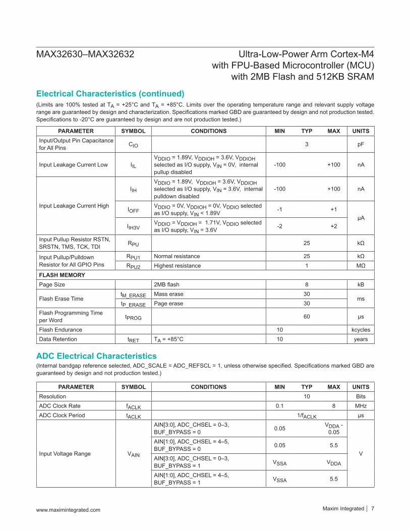
(Limits are 100% tested at TA = +25°C and TA = +85°C. Limits over the operating temperature range and relevant supply voltage range are guaranteed by design and characterization. Specifications marked GBD are guaranteed by design and not production tested. Specifications to -20°C are guaranteed by design and are not production tested.)
(Internal bandgap reference selected, ADC_SCALE = ADC_REFSCL = 1, unless otherwise specified. Specifications marked GBD are guaranteed by design and not production tested.)
PARAMETER SYMBOL CONDITIONS MIN TYP MAX UNITSInput/Output Pin Capacitance for All Pins CIO 3 pF
Input Leakage Current Low IILVDDIO = 1.89V, VDDIOH = 3.6V, VDDIOH selected as I/O supply, VIN = 0V, internal pullup disabled
-100 +100 nA
Input Leakage Current High
IIHVDDIO = 1.89V, VDDIOH = 3.6V, VDDIOH selected as I/O supply, VIN = 3.6V, internal pulldown disabled
-100 +100 nA
IOFFVDDIO = 0V, VDDIOH = 0V, VDDIO selected as I/O supply, VIN < 1.89V -1 +1
μA IIH3V
VDDIO = VDDIOH = 1.71V, VDDIO selected as I/O supply, VIN = 3.6V -2 +2
Input Pullup Resistor RSTN, SRSTN, TMS, TCK, TDI RPU 25 kΩ
Input Pullup/Pulldown Resistor for All GPIO Pins
RPU1 Normal resistance 25 kΩ RPU2 Highest resistance 1 MΩ
FLASH MEMORYPage Size 2MB flash 8 kB
Flash Erase Time tM_ERASE Mass erase 30
ms tP_ERASE Page erase 30
Flash Programming Time per Word tPROG 60 μs
Flash Endurance 10 kcycles Data Retention tRET TA = +85°C 10 years
PARAMETER SYMBOL CONDITIONS MIN TYP MAX UNITSResolution 10 Bits ADC Clock Rate fACLK 0.1 8 MHz ADC Clock Period tACLK 1/fACLK μs
Input Voltage Range VAIN
AIN[3:0], ADC_CHSEL = 0–3, BUF_BYPASS = 0 0.05 VDDA -
0.05
V
AIN[1:0], ADC_CHSEL = 4–5, BUF_BYPASS = 0 0.05 5.5
AIN[3:0], ADC_CHSEL = 0–3, BUF_BYPASS = 1 VSSA VDDA
AIN[1:0], ADC_CHSEL = 4–5, BUF_BYPASS = 1 VSSA 5.5
Electrical Characteristics (continued)
ADC Electrical Characteristics
www.maximintegrated.com Maxim Integrated │ 7
MAX32630–MAX32632 Ultra-Low-Power Arm Cortex-M4 with FPU-Based Microcontroller (MCU)
with 2MB Flash and 512KB SRAM
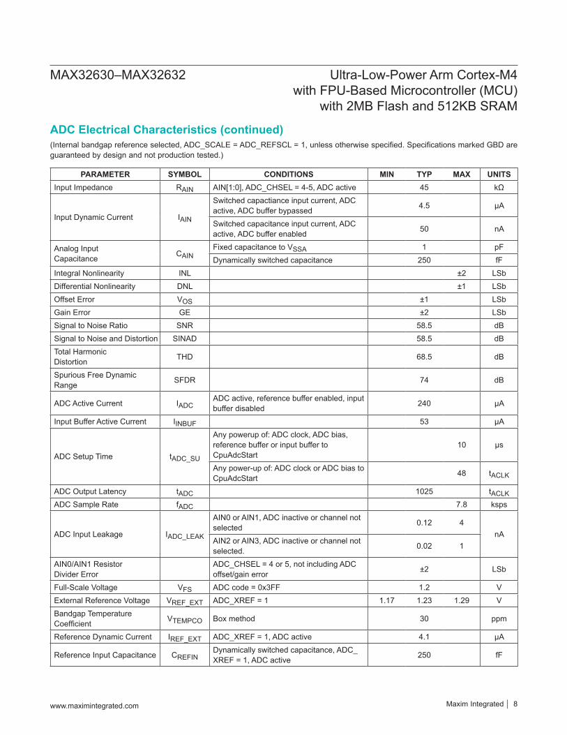
(Internal bandgap reference selected, ADC_SCALE = ADC_REFSCL = 1, unless otherwise specified. Specifications marked GBD are guaranteed by design and not production tested.)
PARAMETER SYMBOL CONDITIONS MIN TYP MAX UNITSInput Impedance RAIN AIN[1:0], ADC_CHSEL = 4-5, ADC active 45 kΩ
Input Dynamic Current IAIN
Switched capactiance input current, ADC active, ADC buffer bypassed 4.5 μA
Switched capacitance input current, ADC active, ADC buffer enabled 50 nA
Analog Input Capacitance CAIN
Fixed capacitance to VSSA 1 pF Dynamically switched capacitance 250 fF
Integral Nonlinearity INL ±2 LSb Differential Nonlinearity DNL ±1 LSb Offset Error VOS ±1 LSb Gain Error GE ±2 LSb Signal to Noise Ratio SNR 58.5 dB Signal to Noise and Distortion SINAD 58.5 dB Total Harmonic Distortion THD 68.5 dB
Spurious Free Dynamic Range SFDR 74 dB
ADC Active Current IADCADC active, reference buffer enabled, input buffer disabled 240 µA
Input Buffer Active Current IINBUF 53 μA
ADC Setup Time tADC_SU
Any powerup of: ADC clock, ADC bias, reference buffer or input buffer to CpuAdcStart
10 µs
Any power-up of: ADC clock or ADC bias to CpuAdcStart 48 tACLK
ADC Output Latency tADC 1025 tACLKADC Sample Rate fADC 7.8 ksps
ADC Input Leakage IADC_LEAK
AIN0 or AIN1, ADC inactive or channel not selected 0.12 4
nA AIN2 or AIN3, ADC inactive or channel not selected. 0.02 1
AIN0/AIN1 Resistor Divider Error
ADC_CHSEL = 4 or 5, not including ADC offset/gain error ±2 LSb
Full-Scale Voltage VFS ADC code = 0x3FF 1.2 V External Reference Voltage VREF_EXT ADC_XREF = 1 1.17 1.23 1.29 V Bandgap Temperature Coefficient VTEMPCO Box method 30 ppm
Reference Dynamic Current IREF_EXT ADC_XREF = 1, ADC active 4.1 μA
Reference Input Capacitance CREFINDynamically switched capacitance, ADC_XREF = 1, ADC active 250 fF
ADC Electrical Characteristics (continued)
www.maximintegrated.com Maxim Integrated │ 8
MAX32630–MAX32632 Ultra-Low-Power Arm Cortex-M4 with FPU-Based Microcontroller (MCU)
with 2MB Flash and 512KB SRAM
(Guaranteed by design and not production tested.)
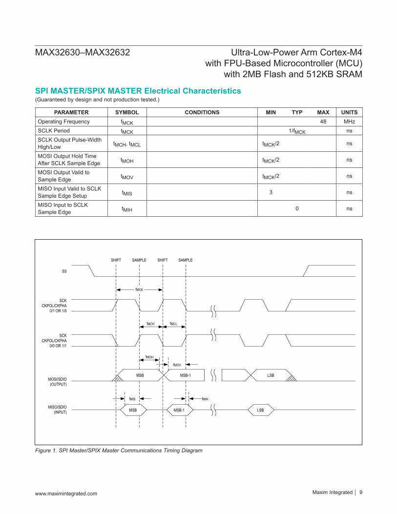
Figure 1. SPI Master/SPIX Master Communications Timing Diagram
PARAMETER SYMBOL CONDITIONS MIN TYP MAX UNITSOperating Frequency fMCK 48 MHz SCLK Period tMCK 1/fMCK ns SCLK Output Pulse-Width High/Low tMCH, tMCL tMCK/2 ns
MOSI Output Hold Time After SCLK Sample Edge tMOH tMCK/2 ns
MOSI Output Valid to Sample Edge tMOV tMCK/2 ns
MISO Input Valid to SCLK Sample Edge Setup tMIS 3 ns
MISO Input to SCLK Sample Edge tMIH 0 ns
SS
SCKCKPOL/CKPHA
0/1 OR 1/0
SCKCKPOL/CKPHA
0/0 OR 1/1
MOSI/SDIO (OUTPUT)
LSB
LSB
SHIFT SAMPLE SHIFT SAMPLE
MSB MSB-1
MSB MSB-1
tMCK
tMCH tMCL
tMOH
tMOV
tMIS tMIH
MISO/SDIO(INPUT)
SPI MASTER/SPIX MASTER Electrical Characteristics
www.maximintegrated.com Maxim Integrated │ 9
MAX32630–MAX32632 Ultra-Low-Power Arm Cortex-M4 with FPU-Based Microcontroller (MCU)
with 2MB Flash and 512KB SRAM
(Guaranteed by design and not production tested.)
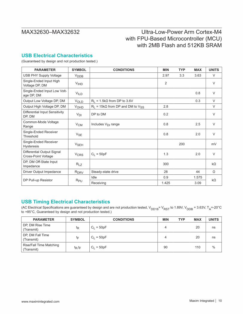
(AC Electrical Specifications are guaranteed by design and are not production tested, VDD18= VRST to 1.89V, VDDB = 3.63V, TA=-20°C to +85°C, Guaranteed by design and not production tested.)
PARAMETER SYMBOL CONDITIONS MIN TYP MAX UNITSUSB PHY Supply Voltage VDDB 2.97 3.3 3.63 V Single-Ended Input High Voltage DP, DM VIHD 2 V
Single-Ended Input Low Volt-age DP, DM VILD 0.8 V
Output Low Voltage DP, DM VOLD RL = 1.5kΩ from DP to 3.6V 0.3 V Output High Voltage DP, DM VOHD RL = 15kΩ from DP and DM to VSS 2.8 V Differential Input Sensitivity DP, DM VDI DP to DM 0.2 V
Common-Mode Voltage Range VCM Includes VDI range 0.8 2.5 V
Single-Ended Receiver Threshold VSE 0.8 2.0 V
Single-Ended Receiver Hysteresis VSEH 200 mV
Differential Output Signal Cross-Point Voltage VCRS CL = 50pF 1.3 2.0 V
DP, DM Off-State Input Impedance RLZ 300 kΩ
Driver Output Impedance RDRV Steady-state drive 28 44 Ω
DP Pull-up Resistor RPUIdle 0.9 1.575
kΩ Receiving 1.425 3.09
PARAMETER SYMBOL CONDITIONS MIN TYP MAX UNITSDP, DM Rise Time (Transmit) tR CL = 50pF 4 20 ns
DP, DM Fall Time (Transmit) tF CL = 50pF 4 20 ns
Rise/Fall Time Matching (Transmit) tR,tF CL = 50pF 90 110 %
USB Electrical Characteristics
USB Timing Electrical Characteristics
www.maximintegrated.com Maxim Integrated │ 10
MAX32630–MAX32632 Ultra-Low-Power Arm Cortex-M4 with FPU-Based Microcontroller (MCU)
with 2MB Flash and 512KB SRAM
(Guaranteed by design and not production tested.)
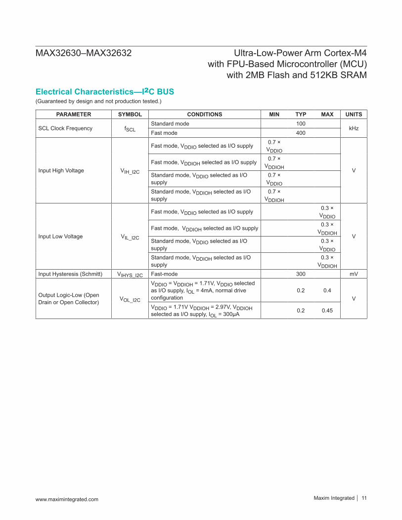
PARAMETER SYMBOL CONDITIONS MIN TYP MAX UNITS
SCL Clock Frequency fSCLStandard mode 100
kHz Fast mode 400
Input High Voltage VIH_I2C
Fast mode, VDDIO selected as I/O supply 0.7 × VDDIO
V Fast mode, VDDIOH selected as I/O supply 0.7 ×
VDDIOHStandard mode, VDDIO selected as I/O supply
0.7 × VDDIO
Standard mode, VDDIOH selected as I/O supply
0.7 × VDDIOH
Input Low Voltage VIL_I2C
Fast mode, VDDIO selected as I/O supply 0.3 × VDDIO
V Fast mode, VDDIOH selected as I/O supply 0.3 ×
VDDIOHStandard mode, VDDIO selected as I/O supply
0.3 × VDDIO
Standard mode, VDDIOH selected as I/O supply
0.3 × VDDIOH
Input Hysteresis (Schmitt) VIHYS_I2C Fast-mode 300 mV
Output Logic-Low (Open Drain or Open Collector) VOL_I2C
VDDIO = VDDIOH = 1.71V, VDDIO selected as I/O supply, IOL = 4mA, normal drive configuration
0.2 0.4V
VDDIO = 1.71V VDDIOH = 2.97V, VDDIOH selected as I/O supply, IOL = 300μA 0.2 0.45
Electrical Characteristics—I2C BUS
www.maximintegrated.com Maxim Integrated │ 11
MAX32630–MAX32632 Ultra-Low-Power Arm Cortex-M4 with FPU-Based Microcontroller (MCU)
with 2MB Flash and 512KB SRAM
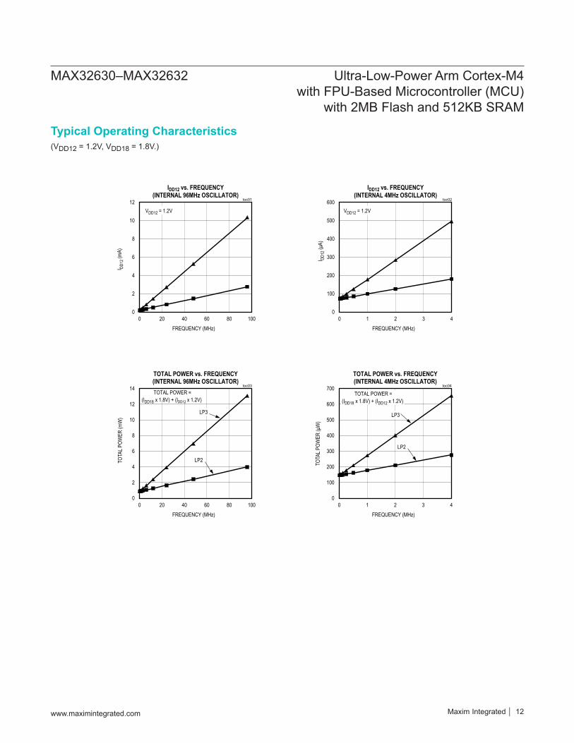
(VDD12 = 1.2V, VDD18 = 1.8V.)
Typical Operating Characteristics
0
2
4
6
8
10
12
0 20 40 60 80 100
I DD12
(mA)
FREQUENCY (MHz)
IDD12 vs. FREQUENCY(INTERNAL 96MHz OSCILLATOR)
toc01
VDD12 = 1.2V
0
100
200
300
400
500
600
0 1 2 3 4I DD
12(μ
A)FREQUENCY (MHz)
IDD12 vs. FREQUENCY(INTERNAL 4MHz OSCILLATOR)
toc02
VDD12 = 1.2V
0
2
4
6
8
10
12
14
0 20 40 60 80 100
TOTA
L POW
ER (m
W)
FREQUENCY (MHz)
TOTAL POWER vs. FREQUENCY(INTERNAL 96MHz OSCILLATOR)
toc03
LP3
LP2
TOTAL POWER = (IDD18 x 1.8V) + (IDD12 x 1.2V)
0
100
200
300
400
500
600
700
0 1 2 3 4
TOTA
L POW
ER (μ
W)
FREQUENCY (MHz)
TOTAL POWER vs. FREQUENCY(INTERNAL 4MHz OSCILLATOR)
toc04
LP2
LP3
TOTAL POWER = (IDD18 x 1.8V) + (IDD12 x 1.2V)
Maxim Integrated │ 12www.maximintegrated.com
MAX32630–MAX32632 Ultra-Low-Power Arm Cortex-M4 with FPU-Based Microcontroller (MCU)
with 2MB Flash and 512KB SRAM
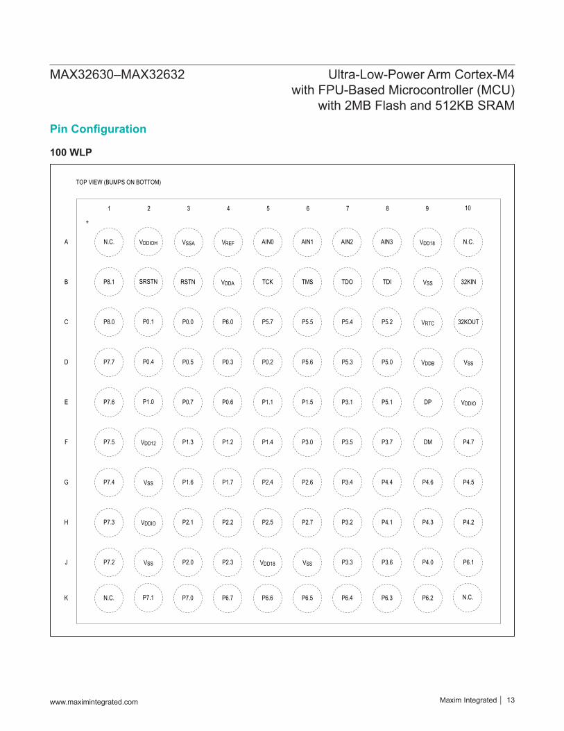
N.C. VSSA VREF AIN0 AIN1 AIN2 AIN3 VDD18
P8.1 RSTN VDDA TCK TMS TDO TDI VSS
P8.0 P0.0 P6.0 P5.7 P5.5 P5.4 P5.2 VRTC
P7.7 P0.5 P0.3 P0.2 P5.6 P5.3 P5.0 VDDB
P7.6 P0.7 P0.6 P1.1 P1.5 P3.1 P5.1 DP
P7.5 P1.3 P1.2 P1.4 P3.0 P3.5 P3.7 DM
P7.4 P1.6 P1.7 P2.4 P2.6 P3.4 P4.4 P4.6
P7.3 P2.1 P2.2 P2.5 P2.7 P3.2 P4.1 P4.3
P7.2 P2.0 P2.3 VDD18 VSS P3.3 P3.6 P4.0
1 2 3 4 5 6 7 8
A
B
C
D
E
F
G
H
J
+
TOP VIEW (BUMPS ON BOTTOM)
N.C.
32KIN
32KOUT
VSS
VDDIO
P4.7
P4.5
P4.2
P6.1
9 10
N.C. P7.0 P6.7 P6.6 P6.5 P6.4 P6.3 P6.2K N.C.
VDDIOH
SRSTN
P0.1
P0.4
P1.0
VDD12
VSS
VDDIO
VSS
P7.1
100 WLP
Pin Configuration
100 WLP
www.maximintegrated.com Maxim Integrated │ 13
MAX32630–MAX32632 Ultra-Low-Power Arm Cortex-M4 with FPU-Based Microcontroller (MCU)
with 2MB Flash and 512KB SRAM
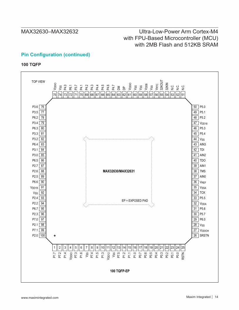
Pin Configuration (continued)
100 TQFP
TOP VIEW
V DDI
O
100 TQFP-EP
MAX32630/MAX32631
V SS
P4.0
P6.1
P3.7
P4.1
P4.2
P4.3
P4.4
P4.5
P4.6
P4.7
DM DP V DDI
O
V SS
V SS
V DDB
V SS
V RTC
P5.0P5.1P5.2VDD18P5.3P5.4VSSAIN3TDIAIN2TDOAIN1TMSAIN0VREF
VSSATCKP5.5VDDAP5.6P5.7P6.0VSS
VDDIOHSRSTN
P1.7
P7.2
P1.4
V DDI
OP7
.3P1
.6V S
SP7
.4P1
.5P1
.3V D
D12
V SS
P7.5
P1.2
P1.1
P1.0
P0.7
P0.6
P0.5
P0.4
P3.6P3.5P6.2P3.4P6.3P3.3P3.2P6.4P3.1P3.0P6.5P2.7P2.6P2.5P6.6
VDD18
VSSP2.4P2.2P6.7P2.3P7.0P2.1P7.1P2.0
P0.3
P0.2
P0.1
P0.0
RSTN
32KO
UT32
KIN
N .C.
N .C.
N.C.
+
75 74 73 72 71 70 69 68 67 66 65 64 63 62 61 60 59 58 57 56
50494847464544434241403938373635343332313029282726
1 2 3 4 5 6 7 8 9 10 11 12 13 14 15 16 17 18 19 20
767778798081828384858687888990919293949596979899
100
21 22 23 24 25
55 54 53 52 51
EP = EXPOSED PAD
www.maximintegrated.com Maxim Integrated │ 14
MAX32630–MAX32632 Ultra-Low-Power Arm Cortex-M4 with FPU-Based Microcontroller (MCU)
with 2MB Flash and 512KB SRAM
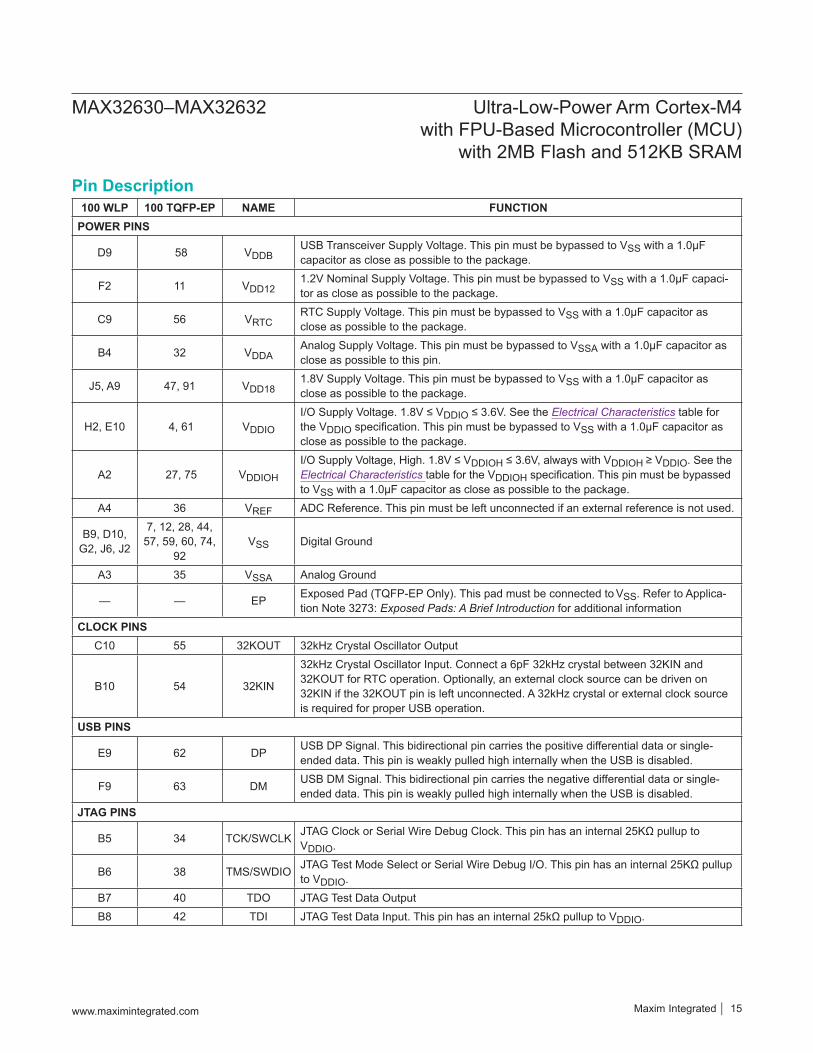
100 WLP 100 TQFP-EP NAME FUNCTIONPOWER PINS
D9 58 VDDBUSB Transceiver Supply Voltage. This pin must be bypassed to VSS with a 1.0μF capacitor as close as possible to the package.
F2 11 VDD121.2V Nominal Supply Voltage. This pin must be bypassed to VSS with a 1.0μF capaci-tor as close as possible to the package.
C9 56 VRTCRTC Supply Voltage. This pin must be bypassed to VSS with a 1.0μF capacitor as close as possible to the package.
B4 32 VDDAAnalog Supply Voltage. This pin must be bypassed to VSSA with a 1.0μF capacitor as close as possible to this pin.
J5, A9 47, 91 VDD181.8V Supply Voltage. This pin must be bypassed to VSS with a 1.0μF capacitor as close as possible to the package.
H2, E10 4, 61 VDDIO
I/O Supply Voltage. 1.8V ≤ VDDIO ≤ 3.6V. See the Electrical Characteristics table for the VDDIO specification. This pin must be bypassed to VSS with a 1.0μF capacitor as close as possible to the package.
A2 27, 75 VDDIOH
I/O Supply Voltage, High. 1.8V ≤ VDDIOH ≤ 3.6V, always with VDDIOH ≥ VDDIO. See the Electrical Characteristics table for the VDDIOH specification. This pin must be bypassed to VSS with a 1.0μF capacitor as close as possible to the package.
A4 36 VREF ADC Reference. This pin must be left unconnected if an external reference is not used.
B9, D10, G2, J6, J2
7, 12, 28, 44, 57, 59, 60, 74,
92VSS Digital Ground
A3 35 VSSA Analog Ground
— — EP Exposed Pad (TQFP-EP Only). This pad must be connected to VSS. Refer to Applica-tion Note 3273: Exposed Pads: A Brief Introduction for additional information
CLOCK PINSC10 55 32KOUT 32kHz Crystal Oscillator Output
B10 54 32KIN
32kHz Crystal Oscillator Input. Connect a 6pF 32kHz crystal between 32KIN and 32KOUT for RTC operation. Optionally, an external clock source can be driven on 32KIN if the 32KOUT pin is left unconnected. A 32kHz crystal or external clock source is required for proper USB operation.
USB PINS
E9 62 DP USB DP Signal. This bidirectional pin carries the positive differential data or single-ended data. This pin is weakly pulled high internally when the USB is disabled.
F9 63 DM USB DM Signal. This bidirectional pin carries the negative differential data or single-ended data. This pin is weakly pulled high internally when the USB is disabled.
JTAG PINS
B5 34 TCK/SWCLK JTAG Clock or Serial Wire Debug Clock. This pin has an internal 25KΩ pullup to VDDIO.
B6 38 TMS/SWDIO JTAG Test Mode Select or Serial Wire Debug I/O. This pin has an internal 25KΩ pullup to VDDIO.
B7 40 TDO JTAG Test Data Output B8 42 TDI JTAG Test Data Input. This pin has an internal 25kΩ pullup to VDDIO.
Pin Description
www.maximintegrated.com Maxim Integrated │ 15
MAX32630–MAX32632 Ultra-Low-Power Arm Cortex-M4 with FPU-Based Microcontroller (MCU)
with 2MB Flash and 512KB SRAM
100 WLP 100 TQFP-EP NAME FUNCTIONRESET PINS
B3 25 RSTN
Hardware Power Reset (Active-Low) Input. The device remains in reset while this pin is in its active state. When the pin transitions to its inactive state, the device performs a POR reset (resetting all logic on all supplies except for real-time clock circuitry) and begins ex-ecution. This pin is internally connected with an internal 25kΩ pullup to the VRTC supply. This pin should be left unconnected if the system design does not provide a reset signal to the device.
B2 26 SRSTN
Software Reset, Active-Low Input/Output. The device remains in software reset while this pin is in its active state. When the pin transitions to its inactive state, the device performs a reset to the Arm CPU, digital registers and peripherals (resetting most of the core logic on the VDD12 supply). This reset does not affect the POR only registers, RTC logic, Arm debug engine or JTAG debugger allowing for a soft reset without having to reconfigure all registers.
After the device senses SRSTN as a logic 0, the pin automatically reconfigures as an output sourcing a logic 0. The device continues to output for 6 system clock cycles and then repeats the input sensing/output driving until SRSTN is sensed inactive.
This pin is internally connected with an internal 25kΩ pullup to the VDDIO supply. This pin should be left unconnected if the system design does not provide a reset signal to the device.
GENERAL-PURPOSE I/O AND SPECIAL FUNCTIONS (See the Applications Information section for GPIO Matrix)C3 24 P0.0 GPIO Port 0.0 C2 23 P0.1 GPIO Port 0.1 D5 22 P0.2 GPIO Port 0.2 D4 21 P0.3 GPIO Port 0.3 D2 20 P0.4 GPIO Port 0.4 D3 19 P0.5 GPIO Port 0.5 E4 18 P0.6 GPIO Port 0.6 E3 17 P0.7 GPIO Port 0.7 E2 16 P1.0 GPIO Port 1.0 E5 15 P1.1 GPIO Port 1.1 F4 14 P1.2 GPIO Port 1.2 F3 10 P1.3 GPIO Port 1.3 F5 3 P1.4 GPIO Port 1.4 E6 9 P1.5 GPIO Port 1.5 G3 6 P1.6 GPIO Port 1.6 G4 1 P1.7 GPIO Port 1.7 J3 100 P2.0 GPIO Port 2.0 H3 98 P2.1 GPIO Port 2.1 H4 94 P2.2 GPIO Port 2.2 J4 96 P2.3 GPIO Port 2.3 G5 93 P2.4 GPIO Port 2.4 H5 89 P2.5 GPIO Port 2.5
Bump Description (continued)
www.maximintegrated.com Maxim Integrated │ 16
MAX32630–MAX32632 Ultra-Low-Power Arm Cortex-M4 with FPU-Based Microcontroller (MCU)
with 2MB Flash and 512KB SRAM
100 WLP 100 TQFP-EP NAME FUNCTIONG6 88 P2.6 GPIO Port 2.6 H6 87 P2.7 GPIO Port 2.7 F6 85 P3.0 GPIO Port 3.0 E7 84 P3.1 GPIO Port 3.1 H7 82 P3.2 GPIO Port 3.2 J7 81 P3.3 GPIO Port 3.3 G7 79 P3.4 GPIO Port 3.4 F7 77 P3.5 GPIO Port 3.5 J8 76 P3.6 GPIO Port 3.6 F8 71 P3.7 GPIO Port 3.7 J9 73 P4.0 GPIO Port 4.0 H8 70 P4.1 GPIO Port 4.1
H10 69 P4.2 GPIO Port 4.2 H9 68 P4.3 GPIO Port 4.3 G8 67 P4.4 GPIO Port 4.4
G10 66 P4.5 GPIO Port 4.5 G9 65 P4.6 GPIO Port 4.6 F10 64 P4.7 GPIO Port 4.7 D8 50 P5.0 GPIO Port 5.0 E8 49 P5.1 GPIO Port 5.1 C8 48 P5.2 GPIO Port 5.2 D7 46 P5.3 GPIO Port 5.3 C7 45 P5.4 GPIO Port 5.4 C6 33 P5.5 GPIO Port 5.5 D6 31 P5.6 GPIO Port 5.6 C5 30 P5.7 GPIO Port 5.7 C4 29 P6.0 GPIO Port 6.0 J10 72 P6.1 GPIO Port 6.1 K9 78 P6.2 GPIO Port 6.2 K8 80 P6.3 GPIO Port 6.3 K7 83 P6.4 GPIO Port 6.4 K6 86 P6.5 GPIO Port 6.5 K5 90 P6.6 GPIO Port 6.6 K4 95 P6.7 GPIO Port 6.7 K3 97 P7.0 GPIO Port 7.0 K2 99 P7.1 GPIO Port 7.1 J1 2 P7.2 GPIO Port 7.2 H1 5 P7.3 GPIO Port 7.3 G1 8 P7.4 GPIO Port 7.4 F1 13 P7.5 GPIO Port 7.5
Bump Description (continued)
www.maximintegrated.com Maxim Integrated │ 17
MAX32630–MAX32632 Ultra-Low-Power Arm Cortex-M4 with FPU-Based Microcontroller (MCU)
with 2MB Flash and 512KB SRAM
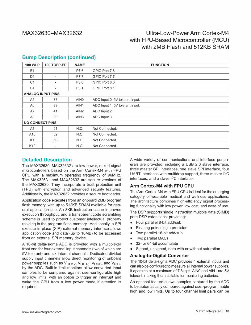
Detailed DescriptionThe MAX32630–MAX32632 are low-power, mixed signal microcontrollers based on the Arm Cortex-M4 with FPU CPU with a maximum operating frequency of 96MHz. The MAX32631 and MAX32632 are secure versions of the MAX32630. They incorporate a trust protection unit (TPU) with encryption and advanced security features. Additionally, the MAX32632 provides a secure bootloader.Application code executes from an onboard 2MB program flash memory, with up to 512KB SRAM available for gen-eral application use. An 8KB instruction cache improves execution throughput, and a transparent code scrambling scheme is used to protect customer intellectual property residing in the program flash memory. Additionally, a SPI execute in place (XIP) external memory interface allows application code and data (up to 16MB) to be accessed from an external SPI memory device.A 10-bit delta-sigma ADC is provided with a multiplexer front end for four external input channels (two of which are 5V tolerant) and six internal channels. Dedicated divided supply input channels allow direct monitoring of onboard power supplies such as VDD12, VDD18, VDDB, and VRTC by the ADC. Built-in limit monitors allow converted input samples to be compared against user-configurable high and low limits, with an option to trigger an interrupt and wake the CPU from a low power mode if attention is required.
A wide variety of communications and interface periph-erals are provided, including a USB 2.0 slave interface, three master SPI interfaces, one slave SPI interface, four UART interfaces with multidrop support, three master I2C interfaces, and a slave I2C interface.
Arm Cortex-M4 with FPU CPUThe Arm Cortex-M4 with FPU CPU is ideal for the emerging category of wearable medical and wellness applications. The architecture combines high-efficiency signal process-ing functionality with low power, low cost, and ease of use.The DSP supports single instruction multiple data (SIMD) path DSP extensions, providing:
● Four parallel 8-bit add/sub ● Floating point single precision ● Two parallel 16-bit add/sub ● Two parallel MACs ● 32- or 64-bit accumulate ● Signed, unsigned, data with or without saturation.
Analog-to-Digital ConverterThe 10-bit delta-sigma ADC provides 4 external inputs and can also be configured to measure all internal power supplies. It operates at a maximum of 7.8ksps. AIN0 and AIN1 are 5V tolerant, making them suitable for monitoring batteries.An optional feature allows samples captured by the ADC to be automatically compared against user-programmable high and low limits. Up to four channel limit pairs can be
100 WLP 100 TQFP-EP NAME FUNCTIONE1 - P7.6 GPIO Port 7.6 D1 - P7.7 GPIO Port 7.7 C1 - P8.0 GPIO Port 8.0 B1 - P8.1 GPIO Port 8.1
ANALOG INPUT PINSA5 37 AIN0 ADC Input 0. 5V tolerant input. A6 39 AIN1 ADC Input 1. 5V tolerant input. A7 41 AIN2 ADC Input 2 A8 39 AIN3 ADC Input 3
NO CONNECT PINSA1 51 N.C. Not Connected.
A10 52 N.C. Not Connected.K1 53 N.C. Not Connected.
K10 - N.C. Not Connected.
Bump Description (continued)
www.maximintegrated.com Maxim Integrated │ 18
MAX32630–MAX32632 Ultra-Low-Power Arm Cortex-M4 with FPU-Based Microcontroller (MCU)
with 2MB Flash and 512KB SRAM
configured in this way. The comparison allows the ADC to trigger an interrupt (and potentially wake the CPU from a low-power sleep mode) when a captured sample goes outside the preprogrammed limit range. Since this comparison is performed directly by the sample limit monitors, it can be performed even while the main CPU is suspended in a low power mode. The ADC reference is selectable:
● Internal bandgap ● External reference ● VDD18. This option disables the reference buffer to
minimize power consumption.
Pulse Train EngineSixteen independent pulse train generators provide either a square wave or a repeating pattern from 2 bits to 32 bits in length. The frequency of each enabled pulse train
generator is also set separately, based on a divide down (divide by 2, divide by 4, divide by 8, etc.) of the input pulse train module clock.Any single pulse train generator or any desired group of pulse train generators can be restarted at the beginning of their patterns and synchronized with one another ensur-ing simultaneous startup. Additionally, each pulse train can operate in a single shot mode.
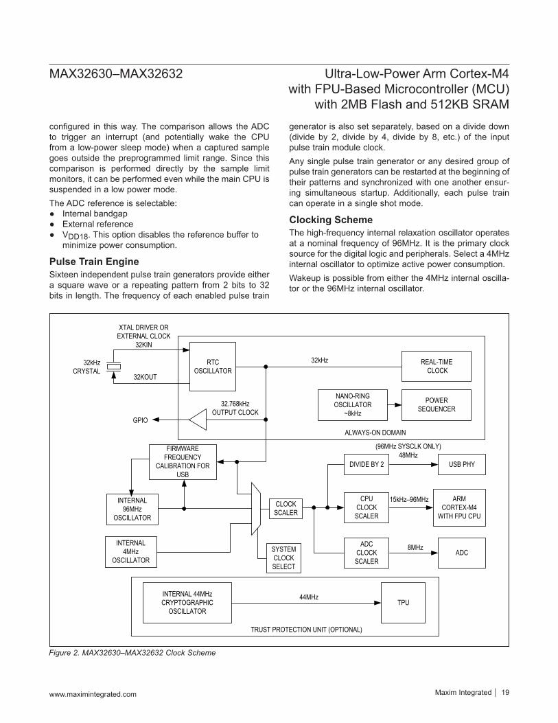
Clocking SchemeThe high-frequency internal relaxation oscillator operates at a nominal frequency of 96MHz. It is the primary clock source for the digital logic and peripherals. Select a 4MHz internal oscillator to optimize active power consumption. Wakeup is possible from either the 4MHz internal oscilla-tor or the 96MHz internal oscillator.
Figure 2. MAX32630–MAX32632 Clock Scheme
REAL-TIME CLOCK
POWER SEQUENCER
USB PHY
NANO-RING OSCILLATOR
~8kHz
FIRMWARE FREQUENCY
CALIBRATION FOR USB
DIVIDE BY 2
CPUCLOCKSCALER
ARM CORTEX-M4
WITH FPU CPU
INTERNAL 96MHz
OSCILLATOR
RTC OSCILLATOR
INTERNAL 44MHz CRYPTOGRAPHIC
OSCILLATORTPU
ADCCLOCKSCALER
ADC
XTAL DRIVER OREXTERNAL CLOCK
32KIN
32KOUT
32kHzCRYSTAL
GPIO
32.768kHz OUTPUT CLOCK
32kHz
ALWAYS-ON DOMAIN
(96MHz SYSCLK ONLY)48MHz
15kHz–96MHz
8MHz
44MHz
TRUST PROTECTION UNIT (OPTIONAL)
INTERNAL 4MHz
OSCILLATOR
CLOCK SCALER
SYSTEM CLOCK SELECT
www.maximintegrated.com Maxim Integrated │ 19
MAX32630–MAX32632 Ultra-Low-Power Arm Cortex-M4 with FPU-Based Microcontroller (MCU)
with 2MB Flash and 512KB SRAM
An external 32.768kHz timebase is required when using the RTC or USB features of the device. The time base can be generated by attaching a 32kHz crystal connected between 32KIN and 32KOUT, or an external clock source can also be applied to the 32KIN pin. The external clock source must meet the electrical/timing requirements in the EC table. The 32kHz output can be directed out to pin P1.7 and remains active in all low power modes including LP0.Interrupt SourcesThe Arm nested vector interrupt controller (NVIC) pro-vides a high-speed, deterministic interrupt response, interrupt masking, and multiple interrupt sources. Each peripheral is connected to the NVIC and can have mul-tiple interrupt flags to indicate the specific source of the interrupt within the peripheral. 55 distinct interrupts can be grouped by firmware into 8 levels of priority (including internal and external interrupts). There are 9 interrupts for the GPIO ports, one for each port.
Real-Time Clock and Wake-Up TimerA real-time clock (RTC) keeps the time of day in absolute seconds. The 32-bit seconds register can count up to approximately 136 years and be translated to calendar format by application software. A time-of-day alarm and independent subsecond alarm can cause an interrupt or wake the device from stop mode The minimum wake-up interval is 244μs. The VRTC supply supports SRAM reten-tion in power mode LP0.
CRC ModuleA CRC hardware module is included to provide fast calcu-lations and data integrity checks by application software.
The CRC module supports both the CRC-16-CCITT and CRC-32 (X32 + X26 + X23 + X22 + X16 + X12 + X11 + X10 + X8 + X7 + X5 + X4 + X2 + X + 1) polynomials.
Watchdog TimersTwo independent watchdog timers (WDT0 and WDT1) with window support are provided. The watchdog timers are independent and have multiple clock source options to ensure system security. The watchdog uses a 32-bit timer with prescaler to generate the watchdog reset. When enabled, the watchdog timers must be written prior to time-out or within a window of time if window mode is enabled. Failure to write the watchdog timer during the programmed timing window results in a watchdog timeout. The WDT0 or WDT1 flags are set on reset if a watchdog expiration caused the system reset. The clock source options for the watchdog timers WDT0 and WDT1 include:
● Scaled system clock ● Real-time clock ● Power management clock
A third watchdog timer (WDT2) is provided for recovery from runaway code or system unresponsiveness. This recovery watchdog uses a 16-bit timer to generate the watchdog reset. When enabled, this watchdog must be written prior to timeout, resulting in a watchdog timeout. The WDT2 flag is set on reset if a watchdog expiration caused the system reset. The clock source for the recov-ery watchdog is the 8kHz nano ring, and the granularity of the timeout period is intended only for system recovery.
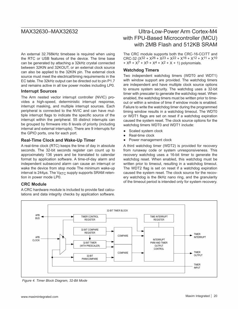
Figure 4. Timer Block Diagram, 32-Bit Mode
TIMER CONTROLREGISTER
32-BIT TIMER(WITH PRESCALER)
32-BIT COMPAREREGISTER
32-BIT PWM/COMPARE
COMPARE
COMPARE
INTERRUPTPWM AND TIMER
OUTPUTCONTROL
TIME INTERRUPTREGISTER
APBBUS
APBCLOCK
TIMERINTERRUPT
TIMEROUTPUT
TIMERINPUT
32-BIT TIMER BLOCK
www.maximintegrated.com Maxim Integrated │ 20
MAX32630–MAX32632 Ultra-Low-Power Arm Cortex-M4 with FPU-Based Microcontroller (MCU)
with 2MB Flash and 512KB SRAM
Programmable TimersSix 32-bit timers provide timing, capture/compare, or gen-eration of pulse-width modulated (PWM) signals. Each of the 32-bit timers can also be split into two 16-bit timers, enabling 12 standard 16-bit timers.32-bit timer features:
● 32-bit up/down autoreload ● Programmable 16-bit prescaler ● PWM output generation ● Capture, compare, and capture/compare capability ● GPIOs can be assigned as external timer inputs,
clock gating or capture, limited to an input frequency of 1/4 of the peripheral clock frequency
● Timer output pin ● Configurable as 2x 16-bit general purpose timers ● Timer interrupt
Serial PeripheralsUSB ControllerThe integrated USB slave controller is compliant with the full-speed (12Mb/s) USB 2.0 specification. The integrated USB physical interface (PHY) reduces board space and system cost. An integrated voltage regulator enables smart switching between the main supply and VDDB when connected to a USB host controller.The USB controller supports DMA for the endpoint buf-fers. A total of 7 endpoint buffers are supported with con-figurable selection of IN or OUT in addition to endpoint 0.An external 32kHz crystal or clock source is required for USB operation, even if the RTC function is not used. Although the USB timing is derived from the internal 96MHz oscillator, the default accuracy is not sufficient for USB operation. Periodic firmware adjustments of the 96MHz oscillator, using the 32kHz timebase as a reference, are necessary to comply with the USB timing requirements.
I2C Master and Slave PortsThe I2C interface is a bidirectional, two-wire serial bus that provides a medium-speed communications network. It can operate as a one-to-one, one-to-many or many-to-many communications medium. Three I2C master engines and one I2C-selectable slave engine interface to a wide variety of I2C-compatible peripherals. These engines support both Standard-mode and Fast-mode I2C standards. The slave engine shares the same I/O port as the master engines and is selectable through the I/O configuration settings. It provides the following features:
● Master or slave mode operation ● Supports standard (7-bit) addressing or 10-bit ad-
dressing ● Support for clock stretching to allow slower slave
devices to operate on higher speed busses ● Multiple transfer rates ● Standard-mode: 100kbps ● Fast-mode: 400kbps ● Internal filter to reject noise spikes ● Receiver FIFO depth of 16 bytes ● Transmitter FIFO depth of 16 bytes
Serial Peripheral Interface—MasterThe SPI master-mode-only (SPIM) interface operates independently in a single or multiple slave system and is fully accessible to the user application. The SPI ports provide a highly configurable, flexible, and efficient interface to communicate with a wide variety of SPI slave devices. The three SPI master ports (SPI0, SPI1, SPI2) support the following features:
● SPI modes (0, 3) for single-bit communication ● 3- or 4-wire mode for single-bit slave device commu-
nication ● Full-duplex operation in single-bit, 4-wire mode ● Dual and Quad I/O supported ● Up to 5 slave select lines per port ● Up to 2 slave ready lines ● Programmable interface timing ● Programmable SCK frequency and duty cycle ● High-speed AHB access to transmit and receive using
32-byte FIFOs ● SS assertion and deassertion timing with respect to
leading/trailing SCK edge
Serial Peripheral Interface—SlaveThe SPI slave (SPIS) port provide a highly configurable, flexible, and efficient interface to communicate with a wide variety of SPI master devices. The SPI slave interface supports the following features:
● Supports SPI modes 0 and 3 ● Full-duplex operation in single-bit, 4-wire mode ● Slave select polarity fixed (active low) ● Dual and Quad I/O supported ● High-speed AHB access to transmit and receive using
32-byte FIFOs ● Four interrupts to monitor FIFO levels
www.maximintegrated.com Maxim Integrated │ 21
MAX32630–MAX32632 Ultra-Low-Power Arm Cortex-M4 with FPU-Based Microcontroller (MCU)
with 2MB Flash and 512KB SRAM
Serial Peripheral Interface Execute in Place (SPIX) MasterThe SPI execute in place (SPIX) master allows the CPU to transparently execute instructions stored in an external SPI flash. Instructions fetched through the SPIX master are cached just like instructions fetched from internal program memory. The SPIX master can also be used to access large amounts of external static data that would otherwise reside in internal data memory.
UARTAll four universal asynchronous receiver-transmitter (UART) interfaces support full-duplex asynchronous com-munication with optional hardware flow control (HFC) modes to prevent data overruns. If HFC mode is enabled on a given port, the system uses two extra pins to imple-ment the industry standard request to send (RTS) and clear to send (CTS) methodology. Each UART is individu-ally programmable.
● 2-wire interface or 4-wire interface with flow control ● 32-byte send/receive FIFO ● Full-duplex operation for asynchronous data transfers ● Programmable interrupt for receive and transmit ● Independent baud-rate generator ● Programmable 9th bit parity support ● Multidrop support ● Start/stop bit support ● Hardware flow control using RTS/CTS ● Maximum baud rate 1843.2kbps
Trust Protection Unit (TPU) (MAX32631/MAX32632)The TPU enhances cryptographic data security for valu-able intellectual property (IP) and data. High-speed, hardware-based cryptographic accelerators perform mathematical computations that support cryptographic algorithms, including:
● AES-128 ● AES-192 ● AES-256 ● 1024-bit DSA ● 2048-bit (CRT)
The device provides a true random number generator that can be used to create cryptographic keys for any application.The MAX32632 also provides a secure bootloader that uses the FIPS186-4 ECDSA algorithm and has a low impact on performance. It guarantees the authenticity and integrity of digitally signed code and data in internal
flash memory, providing assurance that only the intended customer firmware is executed at boot time.The code verification public key is also personalized by the customer and certified by Maxim, allowing the cus-tomer to take ownership of the device.Peripheral Management Unit (PMU)The PMU is a DMA-based link list processing engine that performs operations and data transfers involving memory and/or peripherals in the advanced peripheral bus (APB) and advanced high-performance bus (AHB) peripheral memory space while the main CPU is in a sleep state. This allows low-overhead peripheral operations to be performed without the CPU, significantly reducing overall power consumption. Using the PMU with the CPU in a sleep state provides a lower noise environment critical for obtaining optimum ADC performance.Key features of the PMU engine include:
● Six independent channels with round-robin schedul-ing allows for multiple parallel operations
● Programmed using SRAM-based PMU op codes ● PMU action can be initiated from interrupt conditions
from peripherals without CPU ● Integrated AHB bus master ● Coprocessor-like state machine
Additional DocumentationEngineers must have the following documents to fully use this device:
● This data sheet, containing pin descriptions, feature overviews, and electrical specifications
● The device-appropriate user guide, containing de-tailed information and programming guidelines for core features and peripherals
● Errata sheets for specific revisions noting deviations from published specifications
Development and Technical SupportContact technical support for information about highly versatile, affordable development tools, available from Maxim Integrated and third-party vendors.
● Evaluation kits ● Software development kit ● Compilers ● Integrated development environments (IDEs) ● USB interface modules for programming and debugging
www.maximintegrated.com Maxim Integrated │ 22
MAX32630–MAX32632 Ultra-Low-Power Arm Cortex-M4 with FPU-Based Microcontroller (MCU)
with 2MB Flash and 512KB SRAM
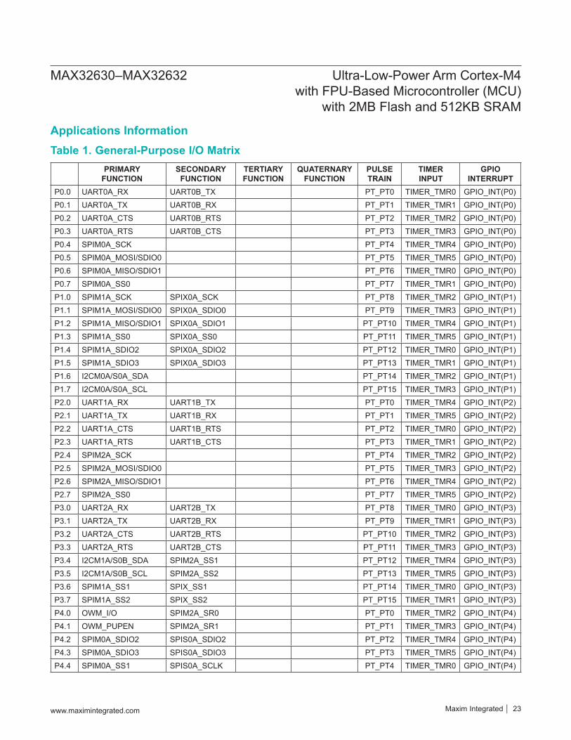
Table 1. General-Purpose I/O Matrix
PRIMARYFUNCTION
SECONDARY FUNCTION
TERTIARY FUNCTION
QUATERNARY FUNCTION
PULSE TRAIN
TIMER INPUT
GPIO INTERRUPT
P0.0 UART0A_RX UART0B_TX PT_PT0 TIMER_TMR0 GPIO_INT(P0)P0.1 UART0A_TX UART0B_RX PT_PT1 TIMER_TMR1 GPIO_INT(P0)P0.2 UART0A_CTS UART0B_RTS PT_PT2 TIMER_TMR2 GPIO_INT(P0)P0.3 UART0A_RTS UART0B_CTS PT_PT3 TIMER_TMR3 GPIO_INT(P0)P0.4 SPIM0A_SCK PT_PT4 TIMER_TMR4 GPIO_INT(P0)P0.5 SPIM0A_MOSI/SDIO0 PT_PT5 TIMER_TMR5 GPIO_INT(P0)P0.6 SPIM0A_MISO/SDIO1 PT_PT6 TIMER_TMR0 GPIO_INT(P0)P0.7 SPIM0A_SS0 PT_PT7 TIMER_TMR1 GPIO_INT(P0)P1.0 SPIM1A_SCK SPIX0A_SCK PT_PT8 TIMER_TMR2 GPIO_INT(P1)P1.1 SPIM1A_MOSI/SDIO0 SPIX0A_SDIO0 PT_PT9 TIMER_TMR3 GPIO_INT(P1)P1.2 SPIM1A_MISO/SDIO1 SPIX0A_SDIO1 PT_PT10 TIMER_TMR4 GPIO_INT(P1)P1.3 SPIM1A_SS0 SPIX0A_SS0 PT_PT11 TIMER_TMR5 GPIO_INT(P1)P1.4 SPIM1A_SDIO2 SPIX0A_SDIO2 PT_PT12 TIMER_TMR0 GPIO_INT(P1)P1.5 SPIM1A_SDIO3 SPIX0A_SDIO3 PT_PT13 TIMER_TMR1 GPIO_INT(P1)P1.6 I2CM0A/S0A_SDA PT_PT14 TIMER_TMR2 GPIO_INT(P1)P1.7 I2CM0A/S0A_SCL PT_PT15 TIMER_TMR3 GPIO_INT(P1)P2.0 UART1A_RX UART1B_TX PT_PT0 TIMER_TMR4 GPIO_INT(P2)P2.1 UART1A_TX UART1B_RX PT_PT1 TIMER_TMR5 GPIO_INT(P2)P2.2 UART1A_CTS UART1B_RTS PT_PT2 TIMER_TMR0 GPIO_INT(P2)P2.3 UART1A_RTS UART1B_CTS PT_PT3 TIMER_TMR1 GPIO_INT(P2)P2.4 SPIM2A_SCK PT_PT4 TIMER_TMR2 GPIO_INT(P2)P2.5 SPIM2A_MOSI/SDIO0 PT_PT5 TIMER_TMR3 GPIO_INT(P2)P2.6 SPIM2A_MISO/SDIO1 PT_PT6 TIMER_TMR4 GPIO_INT(P2)P2.7 SPIM2A_SS0 PT_PT7 TIMER_TMR5 GPIO_INT(P2)P3.0 UART2A_RX UART2B_TX PT_PT8 TIMER_TMR0 GPIO_INT(P3)P3.1 UART2A_TX UART2B_RX PT_PT9 TIMER_TMR1 GPIO_INT(P3)P3.2 UART2A_CTS UART2B_RTS PT_PT10 TIMER_TMR2 GPIO_INT(P3)P3.3 UART2A_RTS UART2B_CTS PT_PT11 TIMER_TMR3 GPIO_INT(P3)P3.4 I2CM1A/S0B_SDA SPIM2A_SS1 PT_PT12 TIMER_TMR4 GPIO_INT(P3)P3.5 I2CM1A/S0B_SCL SPIM2A_SS2 PT_PT13 TIMER_TMR5 GPIO_INT(P3)P3.6 SPIM1A_SS1 SPIX_SS1 PT_PT14 TIMER_TMR0 GPIO_INT(P3)P3.7 SPIM1A_SS2 SPIX_SS2 PT_PT15 TIMER_TMR1 GPIO_INT(P3)P4.0 OWM_I/O SPIM2A_SR0 PT_PT0 TIMER_TMR2 GPIO_INT(P4)P4.1 OWM_PUPEN SPIM2A_SR1 PT_PT1 TIMER_TMR3 GPIO_INT(P4)P4.2 SPIM0A_SDIO2 SPIS0A_SDIO2 PT_PT2 TIMER_TMR4 GPIO_INT(P4)P4.3 SPIM0A_SDIO3 SPIS0A_SDIO3 PT_PT3 TIMER_TMR5 GPIO_INT(P4)P4.4 SPIM0A_SS1 SPIS0A_SCLK PT_PT4 TIMER_TMR0 GPIO_INT(P4)
Applications Information
www.maximintegrated.com Maxim Integrated │ 23
MAX32630–MAX32632 Ultra-Low-Power Arm Cortex-M4 with FPU-Based Microcontroller (MCU)
with 2MB Flash and 512KB SRAM
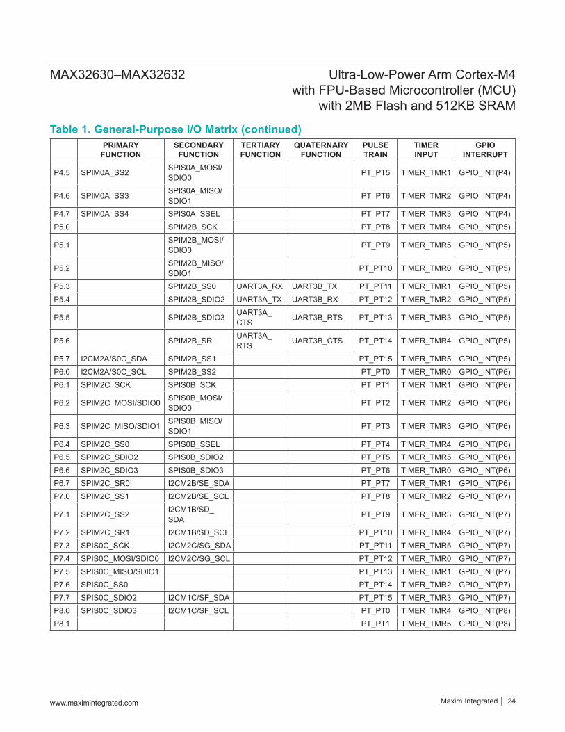
Table 1. General-Purpose I/O Matrix (continued)
PRIMARYFUNCTION
SECONDARY FUNCTION
TERTIARY FUNCTION
QUATERNARY FUNCTION
PULSE TRAIN
TIMER INPUT
GPIO INTERRUPT
P4.5 SPIM0A_SS2 SPIS0A_MOSI/SDIO0 PT_PT5 TIMER_TMR1 GPIO_INT(P4)
P4.6 SPIM0A_SS3 SPIS0A_MISO/SDIO1 PT_PT6 TIMER_TMR2 GPIO_INT(P4)
P4.7 SPIM0A_SS4 SPIS0A_SSEL PT_PT7 TIMER_TMR3 GPIO_INT(P4)P5.0 SPIM2B_SCK PT_PT8 TIMER_TMR4 GPIO_INT(P5)
P5.1 SPIM2B_MOSI/SDIO0 PT_PT9 TIMER_TMR5 GPIO_INT(P5)
P5.2 SPIM2B_MISO/SDIO1 PT_PT10 TIMER_TMR0 GPIO_INT(P5)
P5.3 SPIM2B_SS0 UART3A_RX UART3B_TX PT_PT11 TIMER_TMR1 GPIO_INT(P5)P5.4 SPIM2B_SDIO2 UART3A_TX UART3B_RX PT_PT12 TIMER_TMR2 GPIO_INT(P5)
P5.5 SPIM2B_SDIO3 UART3A_CTS UART3B_RTS PT_PT13 TIMER_TMR3 GPIO_INT(P5)
P5.6 SPIM2B_SR UART3A_RTS UART3B_CTS PT_PT14 TIMER_TMR4 GPIO_INT(P5)
P5.7 I2CM2A/S0C_SDA SPIM2B_SS1 PT_PT15 TIMER_TMR5 GPIO_INT(P5)P6.0 I2CM2A/S0C_SCL SPIM2B_SS2 PT_PT0 TIMER_TMR0 GPIO_INT(P6)P6.1 SPIM2C_SCK SPIS0B_SCK PT_PT1 TIMER_TMR1 GPIO_INT(P6)
P6.2 SPIM2C_MOSI/SDIO0 SPIS0B_MOSI/SDIO0 PT_PT2 TIMER_TMR2 GPIO_INT(P6)
P6.3 SPIM2C_MISO/SDIO1 SPIS0B_MISO/SDIO1 PT_PT3 TIMER_TMR3 GPIO_INT(P6)
P6.4 SPIM2C_SS0 SPIS0B_SSEL PT_PT4 TIMER_TMR4 GPIO_INT(P6)P6.5 SPIM2C_SDIO2 SPIS0B_SDIO2 PT_PT5 TIMER_TMR5 GPIO_INT(P6)P6.6 SPIM2C_SDIO3 SPIS0B_SDIO3 PT_PT6 TIMER_TMR0 GPIO_INT(P6)P6.7 SPIM2C_SR0 I2CM2B/SE_SDA PT_PT7 TIMER_TMR1 GPIO_INT(P6)P7.0 SPIM2C_SS1 I2CM2B/SE_SCL PT_PT8 TIMER_TMR2 GPIO_INT(P7)
P7.1 SPIM2C_SS2 I2CM1B/SD_SDA PT_PT9 TIMER_TMR3 GPIO_INT(P7)
P7.2 SPIM2C_SR1 I2CM1B/SD_SCL PT_PT10 TIMER_TMR4 GPIO_INT(P7)P7.3 SPIS0C_SCK I2CM2C/SG_SDA PT_PT11 TIMER_TMR5 GPIO_INT(P7)P7.4 SPIS0C_MOSI/SDIO0 I2CM2C/SG_SCL PT_PT12 TIMER_TMR0 GPIO_INT(P7)P7.5 SPIS0C_MISO/SDIO1 PT_PT13 TIMER_TMR1 GPIO_INT(P7)P7.6 SPIS0C_SS0 PT_PT14 TIMER_TMR2 GPIO_INT(P7)P7.7 SPIS0C_SDIO2 I2CM1C/SF_SDA PT_PT15 TIMER_TMR3 GPIO_INT(P7)P8.0 SPIS0C_SDIO3 I2CM1C/SF_SCL PT_PT0 TIMER_TMR4 GPIO_INT(P8)P8.1 PT_PT1 TIMER_TMR5 GPIO_INT(P8)
www.maximintegrated.com Maxim Integrated │ 24
MAX32630–MAX32632 Ultra-Low-Power Arm Cortex-M4 with FPU-Based Microcontroller (MCU)
with 2MB Flash and 512KB SRAM
+Denotes a lead(Pb)-free/RoHS-compliant package.T = Tape and reel.
PART FLASH (MB)
SRAM (KB)
TRUST PROTECTION UNIT (TPU)
SECURE BOOTLOADER PIN-PACKAGE
MAX32630IWQ+ 2 512 No No 100 WLPMAX32630IWQ+T 2 512 No No 100 WLPMAX32630ICQ+ 2 512 No No 100 TQFP-EPMAX32631IWQ+ 2 512 Yes No 100 WLPMAX32631IWQ+T 2 512 Yes No 100 WLPMAX32631ICQ+ 2 512 Yes No 100 TQFP-EPMAX32632IWQ+ 2 512 Yes Yes 100 WLPMAX32632IWQ+T 2 512 Yes Yes 100 WLP
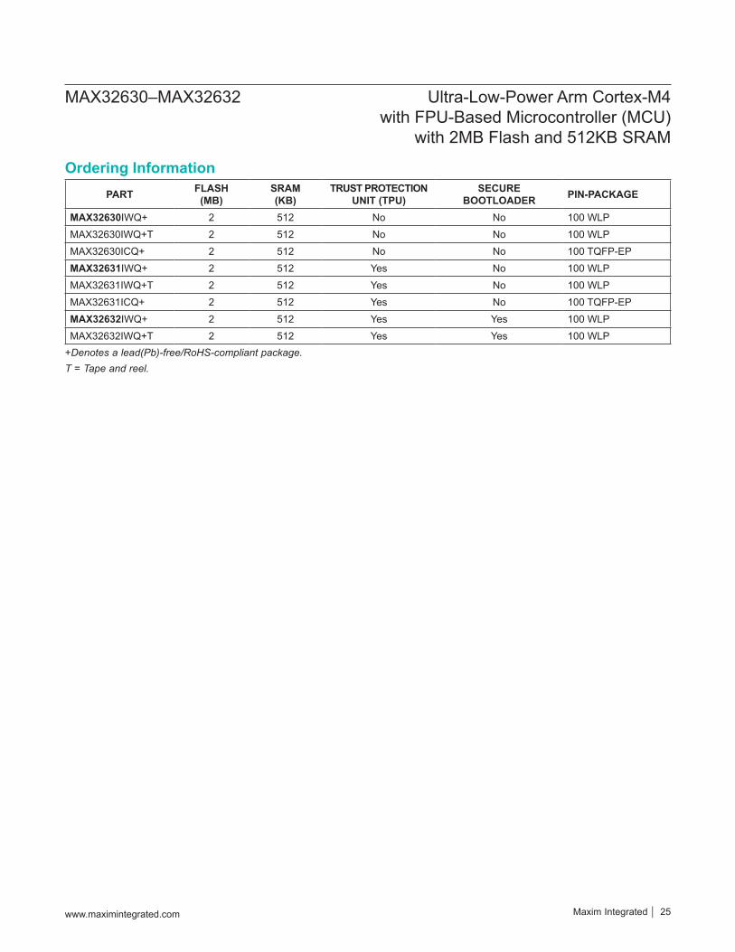
Ordering Information
www.maximintegrated.com Maxim Integrated │ 25
MAX32630–MAX32632 Ultra-Low-Power Arm Cortex-M4 with FPU-Based Microcontroller (MCU)
with 2MB Flash and 512KB SRAM
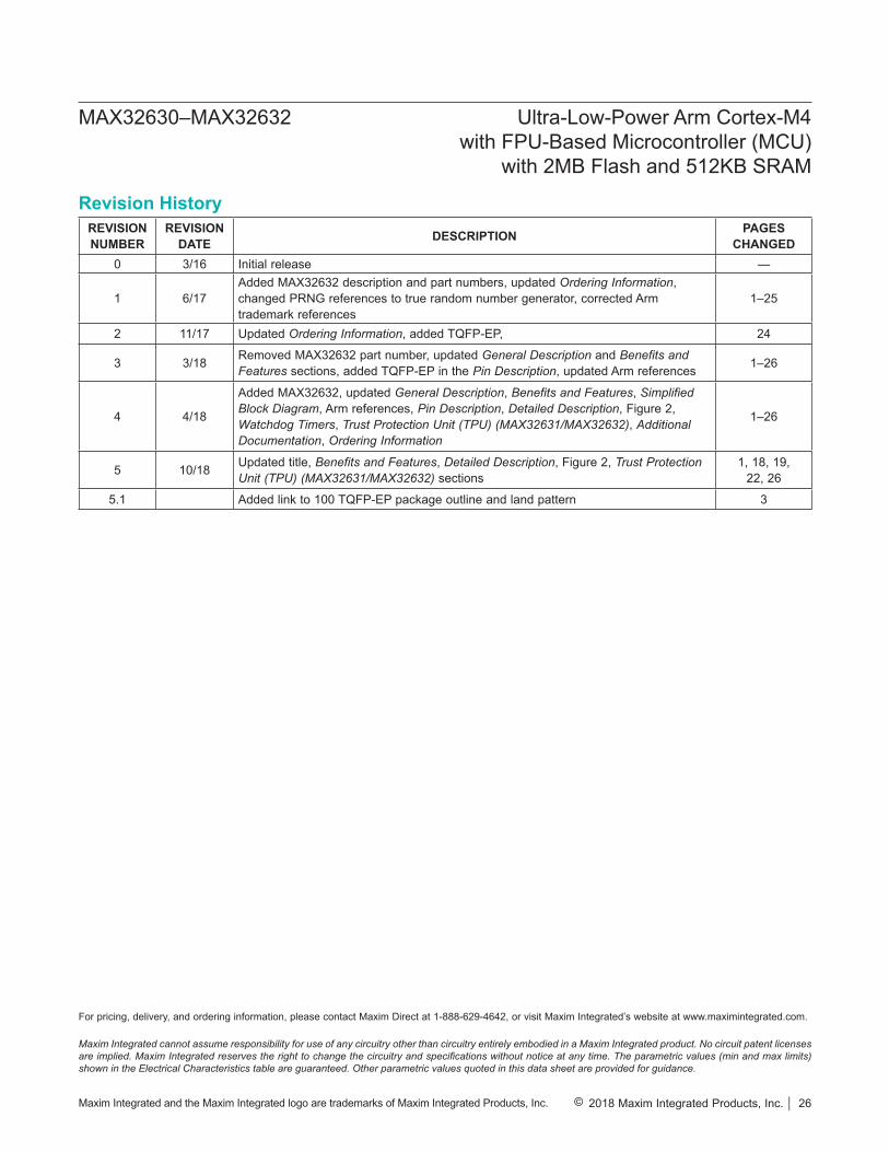
REVISIONNUMBER
REVISIONDATE DESCRIPTION PAGES
CHANGED0 3/16 Initial release —
1 6/17Added MAX32632 description and part numbers, updated Ordering Information, changed PRNG references to true random number generator, corrected Arm trademark references
1–25
2 11/17 Updated Ordering Information, added TQFP-EP, 24
3 3/18 Removed MAX32632 part number, updated General Description and Benefits and Features sections, added TQFP-EP in the Pin Description, updated Arm references 1–26
4 4/18
Added MAX32632, updated General Description, Benefits and Features, Simplified Block Diagram, Arm references, Pin Description, Detailed Description, Figure 2, Watchdog Timers, Trust Protection Unit (TPU) (MAX32631/MAX32632), Additional Documentation, Ordering Information
1–26
5 10/18 Updated title, Benefits and Features, Detailed Description, Figure 2, Trust Protection Unit (TPU) (MAX32631/MAX32632) sections
1, 18, 19, 22, 26
5.1 Added link to 100 TQFP-EP package outline and land pattern 3
Revision History
Maxim Integrated cannot assume responsibility for use of any circuitry other than circuitry entirely embodied in a Maxim Integrated product. No circuit patent licenses are implied. Maxim Integrated reserves the right to change the circuitry and specifications without notice at any time. The parametric values (min and max limits) shown in the Electrical Characteristics table are guaranteed. Other parametric values quoted in this data sheet are provided for guidance.
Maxim Integrated and the Maxim Integrated logo are trademarks of Maxim Integrated Products, Inc. © 2018 Maxim Integrated Products, Inc. │ 26
MAX32630–MAX32632 Ultra-Low-Power Arm Cortex-M4 with FPU-Based Microcontroller (MCU)
with 2MB Flash and 512KB SRAM
For pricing, delivery, and ordering information, please contact Maxim Direct at 1-888-629-4642, or visit Maxim Integrated’s website at www.maximintegrated.com.


![PROCESS CHANGE NOTIFICATION - Mouser Electronics · Nch Vth[V] Nch Idr[μA/μm] Pch Vth[V] Pch Idr[μA/μm] Nch Tr. Vth-Idr Characteristic Pch Tr. Vth-Idr Characteristic Characteristic](https://img.pdfslide.us/doc/110x75/5ea9208bddcafa7fcd4fe0ba/process-change-notification-mouser-electronics-nch-vthv-nch-idram-pch.jpg)