Embed Size (px)
Citation preview
1
KA909A
KA909A-Rev 2.0
Features
• Iris control circuitry with Rail-to-Rail operation
• Continuous Iris Amp Output Current of 80 mA
• Coaxitron (UTC) receiver with DC Restoration
• 200mA full-bridge drivero
amplifier for Day-Night
• Dual comparator for 2 channel general purpose ADC
• Power-on reset: 100mS
Brownout detection • Crystal Oscillator
Applications
CCTV Camera Products
CMOS Camera modules
Portable Electronics
Crystal Oscillators
General Description
The KA909A is optimized for use with analog, HDCCTV and IP
security cameras, and integrates most of the analog signal
conditioning functionality required in advanced camera
modules into a single chip. It is compatible with NextChip, Sony,
Pixim and many other image sensor processors.
The KA909A comprises the following functions:
• Iris Control amplifier with 80mA output drive, controlled by
a DC input signal. Compatible to PWM and DAC outputs
from MCU, DSP and Image Sensor Processors (ISP).
• Day_Night differential drivers with rail to rail drive
performance with up to 200mA source and sink currents.
The Day_Night input is also compatible to PWM, DAC or logic
outputs from MCUs, DSPs and ISPs.
• Coaxitron receiver including a DC restoration stage to
ensure stable operation. The KA909A’s UTC receiver
features on-chip reference, simplifying system design.
• KA909A’s built-in low power analog crystal oscillator circuit
enables the use of low profile devices, saving PCB area.
When operating at 5V VDD, the crystal oscillator requires an
external limiter circuit to maintain low drive levels into the
crystals as many crystals require less than 100uW.
• The Power-on reset combines analog and digital circuitry to
deliver delays of 100ms without requiring external timing
capacitors. This feature enables stable system power-up
while delivering fast reaction time for brown-out detection.
Copyright © 2010, Kiwi Semiconductor Ltd.
PRODUCTION DATA information is current as of publication date. Products conform to specifications per the terms of the Kiwi Semiconductor standard warranty. Production processing does not necessarily include testing of all parameters.
ANALOG SIGNAL CONDITIONING IC FOR CCTV CAMERA SYSTEMS

2
KA909A
KA909A-Rev 2.0
Ordering Information
TA PACKAGE PART NUMBER
-40°C to 85°C 4 mm – 4 mm, 24-pin QFN KA909A
Absolute Maximum Ratings Over operating free-air temperature range unless otherwise noted
UNIT
Supply Voltage 6.5V
Input voltage range on all other pins except AGND/PGND pins with respect to AGND -0.3 V to 3.6 V
Current DRV1, DRV2, IRIS_OUT pins 200 mA
Operating free-air temperature, TA -40°C to 85°C
Maximum junction temperature, TJ 125°C
Storage temperature, Tstg -65°C to 150°C
Lead temperature 1,6 mm (1/16 inch) from case for 10 seconds 260°C
RECOMMENDED OPERATING CONDITIONS
VDD Positive supply voltage 3.1 3.3 / 5.0 5.5 V
DGND Digital Ground (ref to AGND) -0.1 0.1 V

3
KA909A
KA909A-Rev 2.0
Functional Pin Description
KA909A Pin Name Pin Function
1 DAY_NIGHT1 H-bridge driver amplifier main Input
2 VDDD Digital Power Supply
3 DRV_1 H-Bridge Positive Output
4 DRV_2 H-Bridge Negative Output
5 GNDD Digital Ground
6 CLK_OUT Clock Output
7 UTC_IN UTC Receiver Input
8 PWM_UTC UTC Reference
9 COMP1 Comparator-1 Output
10 UTC_OUT UTC CMOS level Output
11 COMP2 Comparator-2 Output
12 PWM_COMP Comparator-1 and Comparator-2 Negative Input
13 XT_OUT Crystal Oscillator Output
14 XT_IN Crystal Oscillator Input
15 POR_TAP Power-on Reset Input
16 RESET (BAR) Active-Low Reset Output
17 MID_TAP Midrail Output
18 CNTLM Iris Amplifier Input
19 GNDA Analog Ground
20 IRIS_FB Iris Amplifier Feedback
21 VDDA Analog Power Supply
22 IRIS_OUT Iris Amplifier Output
23 POT1 Comparator-1 Positive Input
24 POT2 Comparator-2 Positive Input
Electrical Characteristics
VDD = 3.3V / 5.0V, TA=-20 to +70 C, typical values are at 25C
VDD = 3.3V VDD = 5V
PARAMETER TEST CONDITION MIN TYP MAX MIN TYP MAX UNIT
I(VDDD) Quiescent current No load 4 10 mA
I(VDDA) Quiescent current No load 10 20 mA
Control signals: DAY_NIGHT
V(IH) High level input voltage IIH = 20uA 3.0 4.5 V
V(IL Low level input voltage IIL = 10uA 0.3 0.5 V
V(STB) Standby input voltage Outputs disabled – High Z
1.2 1.6 2.0 1.8 2.4 3.2 V
Power-on Reset Internal using 3.3V / 5.0V
2.8 (rising), 2.7 (falling) +/-0.1 2.8 (rising), 2.7 (falling) +/-0.1 V
V(TH) Input threshold voltage Brownout (from TAP input)
0.9 1.0 1.1 0.9 1.0 1.1 V
I(out) ) Output current limit Open drain (0.5V VOL)
2 2 mA

4
KA909A
KA909A-Rev 2.0
V(OL) Output Voltage with 1mA pullup
3.3K / 5K pullup
100 100 mV
T(PO) Power-on Delay Internal RC osc generated
80 200 80 200 ms
Day_Night Driver: DRV_1, DRV_2
VDD
V(OL) Low level output voltage I(OL) = 200mA 0.6 0.6 V
V(OH) High level output voltage I(OH) = 200mA 2.7 4.4 V
Comparators: POT_1, POT_2, C(Pot)
Input range 0.0 3.3 0 5 V
Input impedance 10 10 MΩ
Propagation time to comparator output
Comp_1 & Comp_2
400 800 400 800 ns
DC offset 20 20 mV
UTC block: UTC_IN, UTC_OUT
Propagation time to comparator output
75 100 75 100 ns
Input coupling On-chip DC restore
AC AC
Load Capacitance UTC_OUT 30 30 pF
Comparator output Rise & Fall time
15pF load 50 100 ns
UTC Reference Voltage UTC_IN (Zin = 7.5K to GND)
0.7 0.75 0.8 0.7 0.85 0.95 V
Crystal Oscillator:
Frequency of oscillation 1 27 35 1 27 35 MHz
CLKOUT output Voltage V(OL) CMOS logic levels
0.3 0.5 V
CLKOUT output Voltage V(OH) CMOS logic levels
3.0 4.5 V
Rise & Fall time (10% - 90% VDD)
15pF load 5 12 ns
Output Symmetry (50% VDD) 40 60 40 60 %
Output level (pk to pk) 27MHz crystal
1.65 2.5 V
Output level (pk to pk) with external diodes
27MHz crystal
300 450 mV
Output common mode Voltage 1.55 1.65 1.75 2.3 2.5 2.7 V
Iris Control: Iris_Out, Iris_FB
Midrail bias voltage 50K input to buffer
1.55 1.65 1.75 2.4 2.5 2.6 V
Midrail buffer regulation +/- 1mA load +/- 10 +/- 10 mV
I(bias) Midrail buffer (Iout)
1 1 mA
GBW Iris Amplifier 1 1 MHz
I(Iris_Out)max Max source current to Iris device
80 80 mA
V(OH) High level output voltage I(OH) = 80mA 3.1 4.8 V
5
KA909A
KA909A-Rev 2.0
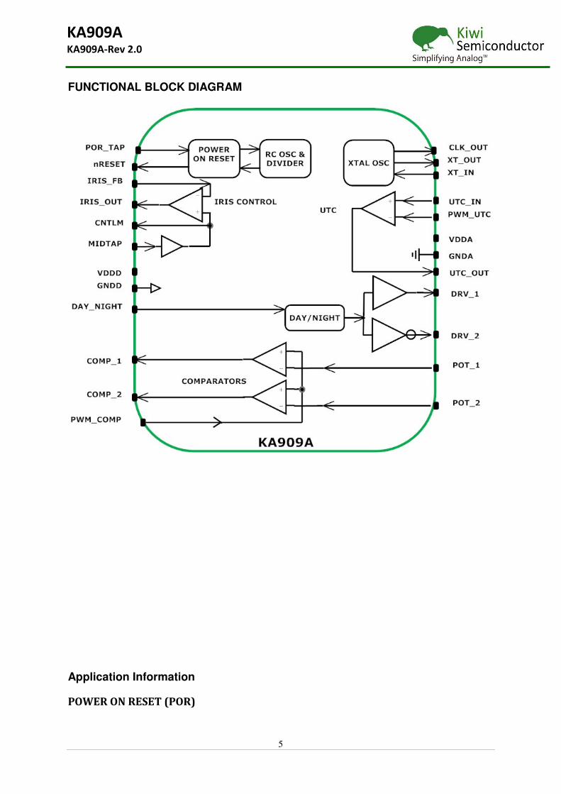
FUNCTIONAL BLOCK DIAGRAM
Application Information
POWER ON RESET (POR)

6
KA909A
KA909A-Rev 2.0
The reset circuit provides under-voltage detection by monitoring both the POR_TAP pin and the
VDD supply voltage. If either the POR_TAP input is below the input threshold voltage, or the
VDD is below the internal supply detection threshold then the RESET output is driven low.
Then, once both thresholds are exceeded, a 100ms timer is started. The RESET output is held
low until the timer expires.
Figure 1: POR configuration
The RESET output type is open drain and requires an external pull-up resistor (R1) to the
supply rail of the connected device (V+). Note: V+ should be less than + 0.6V above VDD to avoid
substrate diode conduction and R1 greater than 3kΩ to provide a low state voltage close to
ground.
A resistor divider on the POR_TAP input sets the reset threshold (Vreset) of the monitored supply
(Vin)
Vreset = 1.0 × (R2+R3)/R3
A typical value for R3 is 10kΩ, in which case
R2 = 10 (Vreset – 1) kΩ.
An optional capacitor, C1, typical value of 2200pF, can be added across R3 to suppress reset
during brief power glitches. The capacitor value should be chosen depending on the specific
power supplies and sensitivities of the circuitry in the application.

7
KA909A
KA909A-Rev 2.0
TRUE DAY NIGHT (TDN) DRIVER
The KA909A includes a full bridge driver suitable for driving TDN actuators providing an almost
rail to rail level drive. The TDN actuator is connected directly across the DRV_1 and DRV_2
outputs. There are two methods of control: a two pin and a single pin method.
Figure 2: Day Night Driver typical application – 2pin control.
Two Pin Control
This requires two lines (GPIO1 and GPIO2) from the controlling device. This method is typically
used when the GPIOs do not have a high impedance state (“Tristate”) option.
The GPIO lines are connected to two 100kΩ resistors to provide a single control voltage. An
external 1MΩ resistor provides biasing to MIDRAIL to define the control voltage when the
inputs have high impedance. See Fig 2.
If the control voltage is greater than 0.9xVDD then DRV_1 will drive high and DRV_2 low
(DRIVE+). If it is below 0.1xVDD then DRV_2 will drive high and DRV_1 low (DRIVE-). If it is
between 0.4xVDD and 0.6xVDD then both outputs are in a high impedance (DRIVE_OFF) state.
Therefore setting both GPIOs high will produce the DRIVE+ state and setting both GPIOs low
will product the DRIVE- state.

8
KA909A
KA909A-Rev 2.0
The DRIVE_OFF state can be achieved by either having both GPIOs in a high impedance state (if
available) or by having one GPIO in a high state and the other in a low state. Table 1: TDN Two
Pin Control Truth Table summarises the response.
GPIO 1 GPIO2 OUTPUT
H L DRIVE_OFF
L H DRIVE_OFF
High Impedance High Impedance DRIVE_OFF
H H DRIVE+
L L DRIVE-
Table 1: TDN Two Pin Control Truth Table
One Pin Control
This only requires one GPIO and is typically used when a high impedance state is available on
the GPIO. It is recommended that the single GPIO line connects to both the DAY_NIGHT_1 and
DAY_NIGHT_2 inputs, although it is possible to connect to only one input with the other left
floating. See Fig 3 for recommended connection. The GPIO is either driven high for DRIVE+ output, low for DRIVE- output or put in high impedance state for DRIVE_OFF state. Table 2:
TDN One Pin Control Truth Table summarises the output response.
GPIO OUTPUT
High Impedance DRIVE_OFF
H DRIVE+
L DRIVE-
Table 2: TDN One Pin Control Truth Table
Figure 3: Day Night Driver typical application – 1pin control

9
KA909A
KA909A-Rev 2.0
AUTO IRIS DRIVER
The KA909A incorporates an optimised amplifier for driving a galavnometer type auto-iris
actuator. By adding external components, the amplifier can be configured as an integrator that
includes the dynamic damping necessary to prevent under and over-shoots on signal
transitions.
Figure 4 shows a typical application schematic.
The DC control voltage (Vcontrol) from the camera processor varies over the range 0-VDD, centred
on VDD/2. The reference voltage for the amplifier is VDD/2, generated from an internal
buffered voltage divider, available at the CNTLM pin.
The control signal is attenuated by the voltage divider comprised of Rp and R2. For example,
values of Rp=10k and R2=2k provide an attenuation factor of 6.
The attenuated signal is presented to the integrator circuit consisting of R1, R3, C1, C2 and R4 in
conjunction with the KA909A amplifier.
Figure 4: Iris control typical application

10
KA909A
KA909A-Rev 2.0
AUTO IRIS DRIVER (CONTINUED)
The governing equations for the iris output are
Viris_ou t = (Vcontrol × t) / (R3 × C1)
for the first phase and
Viris_out = (Vcontrol × t) / (R3 × C2)
for the second phase. Typical values for these components are R1 = 10k, R3 =100k, C1 = 2200pF,
C2 = 0.1uF, R4 = 470R.
The integrator response is bi-phasic. That is in response to a step change at the input C1 the
integrator provides an initial fast response of ~ 7.5V/ms for a 1V step, transitioning to
0.17V/ms thereafter.
Figure 5. Response (VM1) to 100mV (VG1) step change illustrates the response to a 100mV step
change in Vcontrol. A common means of generating the Vcontrol signal is by using a PWM output
from the camera processor. In this case Rp and Cp combine to low-pass filter the PWM signal.
Rp typically remains at 10k and Cp is selected to provide a filter corner frequency significantly
below the PWM frequency.
Figure 5. Response (VM1) to 100mV (VG1) step change
The output from the damping coil provides dynamic feedback for the integrator. It is summed in
as shown. The integrator response then smooths the movement of the iris actuator minimising
ringing. R4, typically 470Ω, controls the sensitivity of the damping coil input.
A decoupling capacitor of about 100nF on the MIDTAP pin is recommended to reject supply rail
noise.

11
KA909A
KA909A-Rev 2.0
UTC COAXITRON RECEIVER
Figure 6. UTC Configuration
The KA909A provides a receiver for extracting UTC Coaxitron data that can be used by the
camera for control of such functions as pan and tilt.
The receiver includes a DC restore function so that both positive DC biased and ground
referenced video signals can be handled. This scheme also provides immunity from changing DC
levels during light to dark or dark to light transitions.
The slicing level is set at nominally 750mV by an on-chip voltage reference. On a 1V p-p video
signal the typical Coaxitron logic levels are approximately 300mV (low) and 1V(high) above the
video sync level. The DC restore circuit references the video sync level to 0V. Therefore the
slicing level is set at the midpoint of the logic levels.
PWM_UTC is an external connection to the slice reference point, provided for adjustment of the
slicing level.
The video signal should be AC coupled to the UTC_IN pin. The coupling corner frequency is
determined by C1 in conjunction with the 100k internal input resistance.
F = 1/(2π x 100k x C1).
A 10nF capacitor provides a corner frequency of 160Hz which is sufficiently high to remove the
effects of DC bias change during light/dark transitions.
R1 provides current limiting during DC restoration and avoids any loading of the video signal. A
1k resistor is suitable and provides minimal attenuation of the video signal at the input to the
KA909A.
Adjustment of the slicing level can be achieved by providing an input to the PWM_UTC pin. This
pin presents a 7.5k input impedance so this needs to be taken into account when driven from a
source with significant source impedance. If driven from a PWM output then the resistance of
the RC filter becomes the source impedance.
The resultant voltage is given by Vslice = 0.75 + 7.5 x (Vpwm – 0.75)/(Rp + 7.5) where R is in kΩ
or alternatively Vpwm = [(Vslice - 0.75)x(Rp + 7.5)/7.5] + 0.75 V
The UTC_OUT provides a digital push-pull output suitable for direct connection to a processor.

12
KA909A
KA909A-Rev 2.0
LOW POWER CRYSTAL OSCILLATOR
The KA909A provides a low power crystal driver. This enables the use of small crystals.
The selection of a crystal to use with the KA909A typically requires:
• Frequency Tolerance: 10ppm max
• Frequency Temperature Stability: 10ppm max
• Aging (over camera life): 10ppm max
• Series resistance: 60 Ω max
• Max drive level: 100uW
Figure 7. Crystal Oscillator Configuration
In order to realise low power drive to the crystal it is necessary to limit the output drive voltage,
while maintaining gain margin in order to ensure reliable start-up. Dual Schottky diode D1 and
coupling capacitor Cd clamp the drive level to less than 800mV p-p without adversely affecting
gain margin. This ensures that the crystal power dissipation is kept well below 100uW and gain
margin is maintained.
D1 should be a low capacitance part (C < 2pF @0V) with Vf <0.4V @2mA. IPS66SB82 from NXP
is recommended.
For higher power rated crystals (>500uW) then D1 and Cd can be omitted (although their
inclusion is still recommended in order to ensure greater drive stability).

13
KA909A
KA909A-Rev 2.0
The crystal manufacturer will typically specify a total load capacitance – CL. This is the required
total load capacitance either side of the crystal (C1 & C2) to achieve the specified crystal
frequency. This is calculated in series, for capacitors, as
1/CL = 1/C1 + 1/C2.
It is recommended that equal value capacitors be used –ie C1 = C2.
Example Calculation: Determining R1, C1 and C2
(Assuming a crystal with load capacitance specification of 10pF)
1. Select R1 = 680 Ω
2. Select C1 & C2. In theory these should each be twice the load cap spec – 2 x 10pF = 20pF.
However select one step lower to allow for parasitic capacitances – therefore select
C1=C2=18pF.
3. Measure the oscillation frequency with selected values. Further adjustment may be
required to achieve close to a nominal 0ppm deviation.
4. Check for adequate gain margin and confirm that crystal dissipation is within
specification as per instructions below.
Checking Gain Margin for Reliable Start-up
Figure 8. Gain Margin Test circuit
To stress test the Gain Margin for reliable start-up insert a resistor, Rseries, as shown above. The
value of this should be approximately four times the crystal maximum series resistance
specification. For example if the crystal specification is 60 Ω (max) then
Rseries = 4 × 60 Ω = 240 Ω.
Confirm that the oscillator starts reliably at room temperature with the increased effective ESR.
Remove Rseries and test at temperature extremes (e.g. -20C & 85C) for reliable start-up and
accurate frequency.

14
KA909A
KA909A-Rev 2.0
Checking Crystal Dissipation
Crystal dissipation is measured by determining the rms current into the crystal. This can be
achieved by inserting a current probe in place of Rseries, or by using a small sense resistor
(10Ω) in Rseries location and using a differential voltage probe. The waveform will not be
perfectly sinusoidal so an rms calculation/conversion will need to be made.
Once the rms current, I, is determined then the maximum power dissipation is I2R, where R is
the maximum ESR specification of the crystal.
Power dissipation can be adjusted with R1, however any change in R1 will require
reconfirmation of gain margin.
Layout Guidelines
Correct pcb layout is important in ensuring reliable and stable operation of the oscillator.
Keep traces as short as possible in order to minimise parasitic capacitances. In particular this
reduces the sensitivity to variations in the dielectric properties of the pcb.
Ensure that noise sources on the board, in particular on the ground plane, are kept away from
the oscillator.
Ensure that the load capacitors and Cd are as close to the KA909A as possible. The ground
return between the capacitors and the KA909A should be as short and direct as possible in
order to avoid interference to the oscillator from surrounding circuitry.
Ensure that the total capacitance loading on the XTAL_OUT to the processor is no more than
15pF.
Frequency Tolerance
The overall frequency tolerance of the oscillator is a stack-up of a number of factors:
1. Crystal tolerance
2. Load capacitor tolerance
3. Board parasitic capacitance variation
4. KA909A input capacitance variation
A typical overall tolerance budget for a camera design is 40ppm. Based on the recommended
crystal specification, the crystal tolerance, plus temperature stability, plus aging consumes
30ppm of this.
Therefore the variation in total capacitance can only account for 10ppm. This requires use of
1% (or better) tolerance capacitors for the load capacitors C1 & C2.
Note that the KA909A input capacitance is approximately 4pF +/- 0.15pF and therefore has a
small but not insignificant influence.

15
KA909A
KA909A-Rev 2.0
EMULATED POTS (COMPARATORS)
Figure 9: Emulated Pots Typical Application
The KA909A includes two comparators that can be used for monitoring the status of two
potentiometers (“emulated pots”), or alternatively for providing the hardware input for an
ADKey Remote or as general purpose analog inputs.
The comparators provide the hardware component of a simple A to D convertor that typically
uses a ramp generated from a PWM output of the controller. The point at which an output
transition occurs on the comparator(s) informs of the analog level on the input.
A typical application circuit for monitoring two potentiometers is shown in Figure 9.
A 10k/100nF filter converts the controller PWM output to a DC level. The filter corner
frequency should be chosen to be well below the PWM frequency.
The DC output from the two external potentiometers is filtered for noise by a 10k/100nF
combination. These components also provide protection against ESD.
The comparator outputs are connected to GPIOs on the controller and monitored for a
transition. Note that the comparator outputs are push-pull and therefore no pullups are
required.

16
KA909A
KA909A-Rev 2.0
PACKAGING
REVISION HISTORY
Revision
Number
Date Description
1 Initial Release
1.1 Dec 5, 2010 2 Dec 5, 2010 Revised specifications
1.2 Jan 15, 2011 3 Jan 15, 2011 Inclusion of application notes and recommended crystals
1.3 Jun 24, 2011 Included parameters for 5V operation
24-Lead Plastic QFN ( 4mm x 4mm )


![標準品 LPM027M128C specification ver02 20170731 · 2017-10-18 · rite black dat ark] and VDDA s and VDDA s Product N ON/OFF SE rising time. (D initialization 1 for internal lat](https://img.pdfslide.us/doc/110x75/5e421e2a4bfc07225b762667/-lpm027m128c-specification-ver02-20170731-2017-10-18-rite-black-dat-ark.jpg)