Embed Size (px)
Citation preview

MISSOURI UNIVERSITY OF SCIENCE & TECHNOLOGY
BCD Arithmetic Implementing the Decimal Adjust Command in WIMP51
CpE-213 Sp 2014 Project 1
3/17/2014
Abstract: The 8051 Microcontroller “decimal adjust” (DA) command was to be implemented for WIMP51. This function was to be programmed so that it could be called by the standard 8051 instruction byte. Moreover, the successful implementation would leave all other functionality of the processor unaffected.

1
Table of Contents
2 Introduction
2 Description of Work
6 Conclusion
7 Appendix A—Test Program
2
Introduction
The 8051 microcontroller has several functions not available in the WIMP51. One such function is “decimal adjust”, which converts single byte hexadecimal numbers to binary-coded decimal (BCD) and allows for decimal arithmetic to be performed on what are in fact binary numbers. The assembly level command for 8051’s decimal adjust is DA; and the machine code is D4H. For convenience, the 8051 instruction was retained in the WIMP51 implementation.
Description of Work
The majority of modifications to the WIMP51 affected only the arithmetic logic unit (ALU). The sole exception was the addition of inputs to the ALU from the least significant two bits of the instruction register (IR1 and IR0), in order to avoid possible conflicts between DA and SETB, since their instructions shared the same most significant four bits. (Time was not taken to determine whether there was actually a conflict here; but during troubleshooting, the extra inputs were added to reduce the number of possible sources of malfunction.)
The algorithm for BCD was simple enough. When two numbers were added, the result was checked to ensure that neither the most significant nibble (MSN) nor the least significant nibble (LSN) was greater than 9H. If either nibble was greater than 9H, then 6H was added to that nibble in order to “correct” the result. Also, if the carry bit (CY) or the auxiliary carry bit (AC) was ‘1’, then 6H was to be added to the MSN or the LSN, respectively.
The main change to the ALU consisted of inserting eight 4:1 MUX’s between the inputs from the auxiliary register (AUX_REG_n) and the B inputs of the 8-bit ripple adder (B_n). The aux register values were routed through inputs 00 and 10 of the corresponding MUX, these two inputs simply being jumpered together. Input 01 of each MUX was connected directly to ground. Inputs 11 were connected to logic 0 (ground) and 1 (VCC) in the following pattern: 0110 0110. The switching input S_0 on each MUX was connected to logic designed to return ‘1’ if and only if the instruction register contained D4H (1101 0100). And inputs S_1 corresponding to the MSN and the LSN of the auxiliary register were made to be ‘1’ whenever the carry bit and the auxiliary carry bit were ‘1’, respectively.
With this configuration, the following five outputs were possible:
Figure 1—BCD MUX Inputs and Outputs
S1 (MSN) S1 (LSN) S0 MUX Outputs X X 0 AUX_REG_7-0
0 0 1 0000 0000
0 1 1 0000 0110
1 0 1 0110 0000
1 1 1 0110 0110

3
The logic circuit designed to control the S_0 inputs was simply an eight-input AND gate with four NOT gates complimenting the values of IR5, IR3, IR1 and IR0, as shown in Figure 2, below. Thus the state of S_0 was ‘1’ only for the D4H instruction, as mentioned before.
Figure 2—DA Instruction Decoding
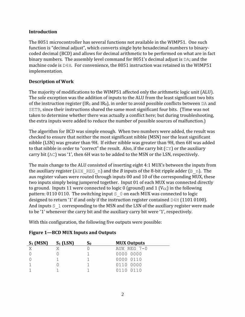
The auxiliary carry used to control the state of the S_1’s in the LSN did not already exist in the WIMP51, and therefore had to be created before DA could be implemented. This was done simply by tapping the internal carry bit from the fourth to the fifth adder in the ripple adder, as shown in Figure 3. It was also necessary to ensure that this AC bit would be latched during the whole DA cycle. To accomplish this, the 2:1 MUX and D flip-flop circuit that was already being used to hold the carry bit was duplicated for the AC. In both cases, the state of the bit would be held until a SETB or CLR instruction was received from the IR.

4
Figure 3—Auxiliary Carry
5
Figure 4—Latching of AC Bit
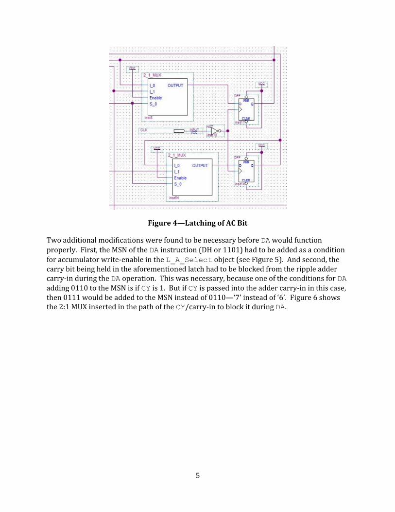
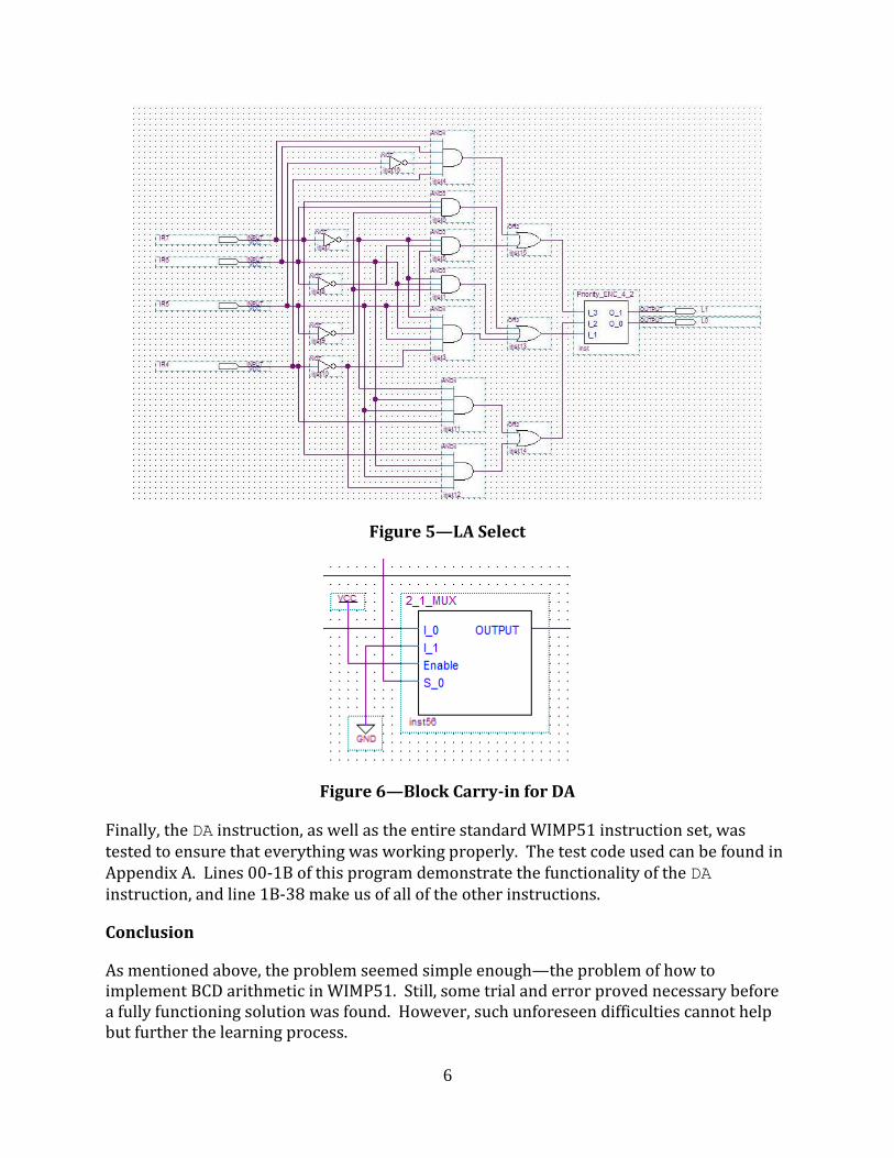
Two additional modifications were found to be necessary before DA would function properly. First, the MSN of the DA instruction (DH or 1101) had to be added as a condition for accumulator write-enable in the L_A_Select object (see Figure 5). And second, the carry bit being held in the aforementioned latch had to be blocked from the ripple adder carry-in during the DA operation. This was necessary, because one of the conditions for DA adding 0110 to the MSN is if CY is 1. But if CY is passed into the adder carry-in in this case, then 0111 would be added to the MSN instead of 0110—‘7’ instead of ‘6’. Figure 6 shows the 2:1 MUX inserted in the path of the CY/carry-in to block it during DA.
6
Figure 5—LA Select
Figure 6—Block Carry-in for DA
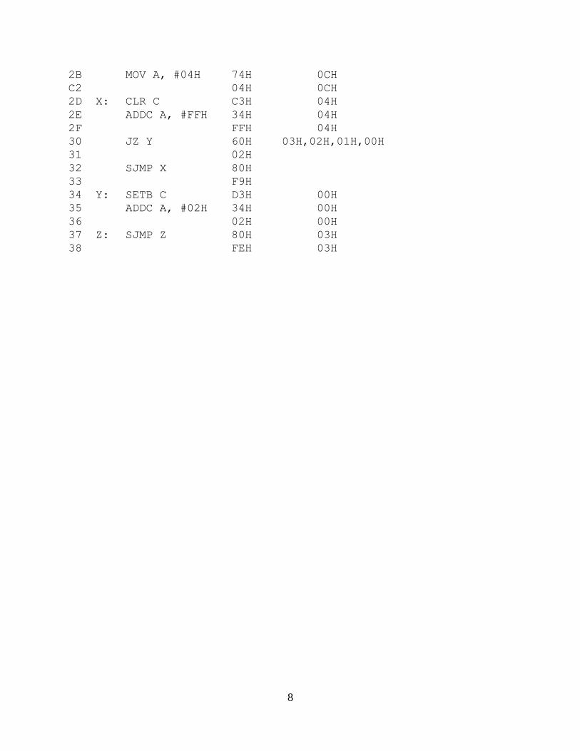
Finally, the DA instruction, as well as the entire standard WIMP51 instruction set, was tested to ensure that everything was working properly. The test code used can be found in Appendix A. Lines 00-1B of this program demonstrate the functionality of the DA instruction, and line 1B-38 make us of all of the other instructions.
Conclusion
As mentioned above, the problem seemed simple enough—the problem of how to implement BCD arithmetic in WIMP51. Still, some trial and error proved necessary before a fully functioning solution was found. However, such unforeseen difficulties cannot help but further the learning process.

7
Appendix A—Test Program
Code Accumulator Notes 00 CLR C C3H 00H 01 MOV A, #00H 74H 00H 02 00H 00H 03 ADDC A, #0AH 34H 00H 04 0AH 00H 05 DA A D4H 0AH LSN>9 06 ADDC A, #F0H 34H 10H 07 F0H 10H 08 DA A D4H 00H C=1 09 CLR C C3H 60H 0A ADDC A, #60 34H 60H 0B 60H 60H 0C DA A D4H C0H MSN>9 0D CLR C C3H 20H 0E SWAP A C4H 20H 0F ADDC A, #0F 34H 02H 10 0FH 02H 11 DA A D4H 11H AC=1 12 CLR C C3H 17H 13 ADDC A, #FB 34H 17H 14 FBH 17H 15 DA A D4H 12H C=AC=1 16 CLR C C3H 78H 17 ADDC A, #44 34H 78H 18 44H 78H 19 DA A D4H BCH MSN, LSN>9 1A CLR C C3H 22H 1B DA A D4H 22H MSN, LSN<9, C=AC=0 1C MOV A, #05H 74H 22H 1D 05H 22H 1E ADDC A, #07H 34H 05H 1F 07H 05H 20 MOV R7, A FFH 0CH 21 ADDC A, R7 3FH 0CH 22 SWAP A C4H 18H 23 MOV A, R7 EFH 81H 24 XRL A, R7 6FH 0CH 25 ORL A, R7 4FH 00H 26 SWAP A C4H 0CH 27 ADDC A, R7 3FH C0H 28 ANL A, R7 5FH CCH 29 SETB C D3H 0CH 2A CLR C C3H 0CH
8
2B MOV A, #04H 74H 0CH C2 04H 0CH 2D X: CLR C C3H 04H 2E ADDC A, #FFH 34H 04H 2F FFH 04H 30 JZ Y 60H 03H,02H,01H,00H 31 02H 32 SJMP X 80H 33 F9H 34 Y: SETB C D3H 00H 35 ADDC A, #02H 34H 00H 36 02H 00H 37 Z: SJMP Z 80H 03H 38 FEH 03H