Embed Size (px)
Citation preview
AVAILABLE
EVALUATION KIT AVAILABLE
Functional Diagrams
Pin Configurations appear at end of data sheet.Functional Diagrams continued at end of data sheet.UCSP is a trademark of Maxim Integrated Products, Inc.
For pricing, delivery, and ordering information, please contact Maxim Direct at 1-888-629-4642, or visit Maxim’s website at www.maximintegrated.com.
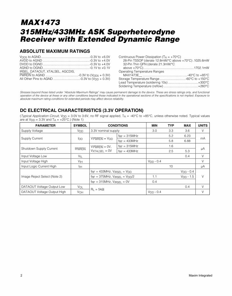
General DescriptionThe MAX1473 fully integrated low-power CMOS super-heterodyne receiver is ideal for receiving amplitude-shift-keyed (ASK) data in the 300MHz to 450MHzfrequency range. Its signal range is from -114dBm to0dBm. With few external components and a low-currentpower-down mode, it is ideal for cost- and power-sensi-tive applications typical in the automotive and consumermarkets. The chip consists of a low-noise amplifier(LNA), a fully differential image-rejection mixer, an on-chip phase-locked-loop (PLL) with integrated voltage-controlled oscillator (VCO), a 10.7MHz IF limitingamplifier stage with received-signal-strength indicator(RSSI), and analog baseband data-recovery circuitry.The MAX1473 also has a discrete one-step automaticgain control (AGC) that drops the LNA gain by 35dBwhen the RF input signal is greater than -57dBm.
The MAX1473 is available in 28-pin TSSOP and 32-pinthin QFN packages. Both versions are specified for theextended (-40°C to +85°C) temperature range.
ApplicationsAutomotive Remote Keyless Entry Security Systems
Garage Door Openers Home Automation
Remote Controls Local Telemetry
Wireless Sensors Systems
Features Optimized for 315MHz or 433MHz ISM Band
Operates from Single 3.3V or 5.0V Supplies
High Dynamic Range with On-Chip AGC
Selectable Image-Rejection Center Frequency
Selectable x64 or x32 fLO/fXTAL Ratio
Low 5.2mA Operating Supply Current
< 2.5µA Low-Current Power-Down Mode forEfficient Power Cycling
250µs Startup Time
Built-In 50dB RF Image Rejection
Receive Sensitivity of -114dBm
315MHz/433MHz ASK SuperheterodyneReceiver with Extended Dynamic Range
28
27
26
25
24
23
22
21
20
19
18
17
16
15
1
2
3
4
5
6
7
8
9
10
11
12
13
14
XTAL2
PWRDN
PDOUT
DATAOUT
VDD5
DSP
AGCDIS
DFFB
OPP
DSN
DFO
IFIN2
IFIN1
XTALSEL
DVDD
DGND
MIXOUT
IRSEL
AGND
MIXIN2
MIXIN1
AVDD
LNAOUT
AGND
LNASRC
LNAIN
AVDD
XTAL1
TSSOPTHIN QFN
TOP VIEW
MAX1473
32 31 30 29 28 27 26
LNAS
RC
LNAI
N
AVDD
XTAL
1
XTAL
2
PWRD
N
PDOU
T
25N.
C.
9 10 11 12 13 14 15
MIX
OUT
DGND
DVDD
AGCD
IS
N.C.
XTAL
SEL
IFIN
1
16IF
IN2
17
18
19
20
21
22
23
DFO
DSN
OPP
DFFB
N.C.
DSP
VDD5
8
7
6
5
4
3
2
IRSEL
AGND
MIXIN2
MIXIN1
AVDD
LNAOUT
AGND
MAX1473
1N.C. 24 DATAOUT
+
+
PART TEMP RANGE PIN-PACKAGE
MAX1473EUI+ -40°C to +85°C 28 TSSOP
MAX1473ETJ+ -40°C to +85°C 32 Thin QFN-EP*
Pin Configurations
Ordering Information
Functional Diagram and Typical Application Circuit appearat end of data sheet.
+Denotes a lead(Pb)-free/RoHS-compliant package.*EP = Exposed pad.
MAX1473
19-2748; Rev 6; 1/12
315MHz/433MHz ASK SuperheterodyneReceiver with Extended Dynamic RangeABSOLUTE MAXIMUM RATINGS
DC ELECTRICAL CHARACTERISTICS (3.3V OPERATION)(Typical Application Circuit, VDD = 3.0V to 3.6V, no RF signal applied, TA = -40°C to +85°C, unless otherwise noted. Typical valuesare at VDD = 3.3V and TA = +25°C.) (Note 1)
Stresses beyond those listed under “Absolute Maximum Ratings” may cause permanent damage to the device. These are stress ratings only, and functionaloperation of the device at these or any other conditions beyond those indicated in the operational sections of the specifications is not implied. Exposure toabsolute maximum rating conditions for extended periods may affect device reliability.
VDD5 to AGND.......................................................-0.3V to +6.0VAVDD to AGND .....................................................-0.3V to +4.0VDVDD to DGND.....................................................-0.3V to +4.0VAGND to DGND.....................................................-0.1V to +0.1VIRSEL, DATAOUT, XTALSEL, AGCDIS, PWRDN to AGND .....................................-0.3V to (VDD5 + 0.3V)All Other Pins to AGND ..............................-0.3V to (VDD + 0.3V)
Continuous Power Dissipation (TA = +70°C)28-Pin TSSOP (derate 12.8mW/°C above +70°C) .1025.6mW32-Pin Thin QFN (derate 21.3mW/°C above +70°C).........................................................1702.1mW
Operating Temperature RangesMAX1473E__ ..................................................-40°C to +85°C
Storage Temperature Range .............................-60°C to +150°CLead Temperature (soldering 10s) ..................................+300°CSoldering Temperature (reflow) .......................................+260°C
PARAMETER SYMBOL CONDITIONS MIN TYP MAX UNITS
Supply Voltage VDD 3.3V nominal supply 3.0 3.3 3.6 V
fRF = 315MHz 5.2 6.23Supply Current IDD V P WRDN = VDD
fRF = 433MHz 5.8 6.88mA
fRF = 315MHz 1.6Shutdown Supply Current IPWRDN
V P WRDN = 0V,VXTALSEL = 0V fRF = 433MHz 2.5 5.3
µA
Input Voltage Low VIL 0.4 V
Input Voltage High VIH VDD - 0.4 V
Input Logic Current High IIH 10 µA
fRF = 433MHz, VIRSEL = VDD VDD - 0.4
fRF = 375MHz, VIRSEL = VDD/2 1.1 VDD - 1.5Image Reject Select (Note 2)
fRF = 315MHz, VIRSEL = 0V 0.4
V
DATAOUT Voltage Output Low VOL 0.4 V
DATAOUT Voltage Output High VOHRL = 5kΩ
VDD - 0.4 V
19-2748; Rev 6; 1/12
MAX1473
2 Maxim Integrated
315MHz/433MHz ASK SuperheterodyneReceiver with Extended Dynamic Range
DC ELECTRICAL CHARACTERISTICS (5.0V OPERATION)(Typical Application Circuit, VDD = 4.5V to 5.5V, no RF signal applied, TA = -40°C to +85°C, unless otherwise noted. Typical valuesare at VDD = 5.0V and TA = +25°C.) (Note 1)
PARAMETER SYMBOL CONDITIONS MIN TYP MAX UNITS
Supply Voltage VDD 5.0V nominal supply 4.5 5.0 5.5 V
fRF = 315MHz 5.2 6.04Supply Current IDD V P WRDN = VDD
fRF = 433MHz 5.7 6.76mA
fRF = 315MHz 2.3Shutdown Supply Current IPWRDN
V P WRDN = 0V,VXTALSEL = 0V fRF = 433MHz 2.8 6.2
µA
Input Voltage Low VIL 0.4 V
Input Voltage High VIH VDD - 0.4 V
Input Logic Current High IIH 10 µA
fRF = 433MHz, VIRSEL = VDD VDD - 0.4
fRF = 375MHz, VIRSEL = VDD/2 1.1 VDD - 1.5Image Reject Select (Note 2)
fRF = 315MHz, VIRSEL = 0V 0.4
V
DATAOUT Voltage Output Low VOL 0.4 V
DATAOUT Voltage Output High VOHRL = 5kΩ
VDD - 0.4 V
AC ELECTRICAL CHARACTERISTICS (Typical Application Circuit, VDD = 3.0V to 3.6V, all RF inputs are referenced to 50Ω, fRF = 315MHz, TA = -40°C to +85°C, unless otherwise noted. Typical values are at VDD = 3.3V and TA = +25°C.) (Note 1).
PARAMETER SYMBOL CONDITIONS MIN TYP MAX UNITS
GENERAL CHARACTERISTICS
Startup Time tONTime for valid signal detection afterV P WRDN = VOH
250 µs
Receiver Input Frequency fRF 300 450 MHz
Maximum Receiver Input Level PRFIN_MAX Modulation depth > 18dB 0 dBm
Sensitivity (Note 3) PRFIN_MIN Peak power level -114 dBm
8 dBAGC Hysteresis LNA gain from low to high
150 ms
LNA IN HIGH-GAIN MODE
Power Gain 16 dB
fRF = 433MHz 1 - j3.4
fRF = 375MHz 1 - j3.9Input Impedance (Note 4) ZIN_LNANormalized to50Ω
fRF = 315MHz 1 - j4.7
1dB Compression Point P1dBLNA -22 dBm
Input-Referred 3rd-OrderIntercept
IIP3LNA -12 dBm
MAX1473
Maxim Integrated 3
315MHz/433MHz ASK SuperheterodyneReceiver with Extended Dynamic RangeAC ELECTRICAL CHARACTERISTICS (continued)(Typical Application Circuit, VDD = 3.0V to 3.6V, all RF inputs are referenced to 50Ω, fRF = 315MHz, TA = -40°C to +85°C, unless otherwise noted. Typical values are at VDD = 3.3V and TA = +25°C.) (Note 1)
PARAMETER SYMBOL CONDITIONS MIN TYP MAX UNITS
LO Signal Feedthrough toAntenna
-80 dBm
Noise Figure NFLNA 2 dB
LNA IN LOW-GAIN MODE
fRF = 433MHz 1 - j3.4
fRF = 375MHz 1 - j3.9Input Impedance (Note 4) ZIN_LNANormalized to50Ω
fRF = 315MHz 1 - j4.7
1dB Compression Point P1dBLNA -10 dBm
Input-Referred 3rd-OrderIntercept
IIP3LNA -7 dBm
LO Signal Feedthrough toAntenna
-80 dBm
Noise Figure NFLNA 2 dB
Power Gain 0 dB
Voltage Gain Reduction AGC enabled (depends on tank Q) 35 dB
MIXER
Input-Referred 3rd-OrderIntercept
IIP3MIX -18 dBm
Output Impedance ZOUT_MIX 330 ΩNoise Figure NFMIX 16 dB
fRF = 433MHz, VIRSEL = VDD 42
fRF = 375MHz, VIRSEL = VDD/2 44Image Rejection(not Including LNA Tank)
fRF = 315MHz, VIRSEL = 0V 44
dB
Conversion Gain 330Ω IF filter load 13 dB
INTERMEDIATE FREQUENCY (IF)
Input Impedance ZIN_IF 330 ΩOperating Frequency fIF Bandpass response 10.7 MHz
3dB Bandwidth 20 MHz
RSSI Linearity ±0.5 dB
RSSI Dynamic Range 80 dB
PRFIN < -120dBm 1.15RSSI Level
PRFIN > 0dBm, AGC enabled 2.35V
RSSI Gain 14.2 mV/dB
LNA gain from low to high 1.45AGC Threshold
LNA gain from high to low 2.05V
MAX1473
4 Maxim Integrated
315MHz/433MHz ASK SuperheterodyneReceiver with Extended Dynamic Range
Note 1: 100% tested at TA = +25°C. Guaranteed by design and characterization over temperature.
Note 2: IRSEL is internally set to 375MHz IR mode. It can be left open when the 375MHz image rejection setting is desired. A 1nF capacitor is recommended in noisy environments.
Note 3: BER = 2 x 10⁻³, Manchester encoded, data rate = 4kbps, IF bandwidth = 280kHz.
Note 4: Input impedance is measured at the LNAIN pin. Note that the impedance includes the 15nH inductive degeneration con-nected from the LNA source to ground. The equivalent input circuit is 50Ω in series with 2.2pF.
Note 5: Crystal oscillator frequency for other RF carrier frequency within the 300MHz to 450MHz range is (fRF - 10.7MHz)/64 for XTALSEL = 0V, and (fRF - 10.7MHz)/32 for XTALSEL = VDD.
AC ELECTRICAL CHARACTERISTICS (continued)(Typical Application Circuit, VDD = 3.0V to 3.6V, all RF inputs are referenced to 50Ω, fRF = 315MHz, TA = -40°C to +85°C, unless otherwise noted. Typical values are at VDD = 3.3V and TA = +25°C.) (Note 1)
PARAMETER SYMBOL CONDITIONS MIN TYP MAX UNITS
DATA FILTER
Maximum Bandwidth BWDF 100 kHz
DATA SLICER
Comparator Bandwidth BWCMP 100 kHz
Output High Voltage VDD5 V
Output Low Voltage 0 V
CRYSTAL OSCILLATOR
VXTALSEL = 0V 6.6128fRF = 433MHz
VXTALSEL = VDD 13.2256MHz
VXTALSEL = 0V 4.7547Crystal Frequency (Note 5) fXTAL
fRF = 315MHzVXTALSEL = VDD 9.5094
MHz
Crystal Tolerance 50 ppm
Input Capacitance From each pin to ground 6.2 pF
Recommended Crystal LoadCapacitance
CLOAD 3 pF
Maximum Crystal LoadCapacitance
CLOAD 10 pF
MAX1473
Maxim Integrated 5
315MHz/433MHz ASK SuperheterodyneReceiver with Extended Dynamic Range
Typical Operating Characteristics(Typical Application Circuit, VDD = 3.3V, fRF = 315MHz, TA = +25°C, unless otherwise noted.)
SUPPLY CURRENTvs. SUPPLY VOLTAGE
MAX
1473
toc0
1
SUPPLY VOLTAGE (V)
SUPP
LY C
URRE
NT (m
A)
3.53.43.33.23.1
5.0
5.1
5.2
5.3
5.4
5.5
5.6
4.93.0 3.6
+105°C
+85°C
+25°C
-40°C
SUPPLY CURRENTvs. RF FREQUENCY
MAX
1473
toc0
2
RF FREQUENCY (MHz)
SUPP
LY C
URRE
NT (m
A)
450400350300
5.0
5.5
6.0
6.5
7.0
4.5250 500
+105°C
+25°C
+85°C
-40°C
100
0.01-121 -118-120 -119 -117 -116 -114
BIT-ERROR RATE vs. AVERAGE RF INPUT POWER
0.1
1
10
MAX
1473
toc0
3
AVERAGE INPUT POWER (dBm)
BIT-
ERRO
R RA
TE (%
)
-115
fRF = 433MHz
fRF = 315MHz
SENSITIVITY vs. TEMPERATURE
MAX
1473
toc0
4
TEMPERATURE (°C)
SENS
ITIV
ITY
(dBm
)
10080-20 0 20 40 60
-116
-114
-112
-110
-108
-106
-104
-102
-100
-118-40 120
PEAK RF INPUT POWER0.2% BERIF BANDWIDTH = 280kHz
fRF = 433MHz
fRF = 315MHz
RSSI vs. RF INPUT POWERM
AX14
73 to
c05
RF INPUT POWER (dBm)
RSSI
(V)
-20-40-60-80-100-120
1.2
1.4
1.6
1.8
2.0
2.2
2.4
1.0-140 0
IF BANDWIDTH = 280kHz
VAGCDIS = 0V
VAGCDIS = VDD
RSSI AND DELTAvs. IF INPUT POWER
MAX1473 toc06
IF INPUT POWER (dBm)
RSSI
(V)
-10-30-50-70
1.2
1.4
1.6
1.8
2.0
2.2
2.4
1.0
DELT
A (d
B)
-2.5
-1.5
-0.5
0.5
1.5
2.5
3.5
-3.5-90 10
DELTA
RSSI
SYSTEM GAIN vs. FREQUENCY
MAX
1473
toc0
7
IF FREQUENCY (MHz)
SYST
EM G
AIN
(dB)
252015105
-20
-10
0
10
20
30
-300 30
UPPERSIDEBAND
LOWERSIDEBAND
FROM RFIN TOMIXOUTfRF = 315MHz
50dB IMAGEREJECTION
IMAGE REJECTION vs. RF FREQUENCY
MAX
1473
toc0
8
RF FREQUENCY (MHz)
IMAG
E RE
JECT
ION
(dB)
430380330
35
40
45
50
55
30280 480
fRF = 433MHz
fRF = 375MHz
fRF = 315MHz
IMAGE REJECTION vs. TEMPERATURE
MAX
1473
toc0
9
TEMPERATURE (°C)
IMAG
E RE
JECT
ION
(dB)
603510-15
41
42
42
43
43
44
44
45
45
41-40 85
fRF = 315MHz
fRF = 375MHz
fRF = 433MHz
MAX1473
6 Maxim Integrated
315MHz/433MHz ASK SuperheterodyneReceiver with Extended Dynamic Range
5
-201 10 100
NORMALIZED IF GAINvs. IF FREQUENCY
-15
MAX
1473
toc1
0
IF FREQUENCY (MHz)
NORM
ALIZ
ED IF
GAI
N (d
B)
-10
-5
0
S11 MAGNITUDE-LOG PLOT OF RFIN
MAX
1473
toc1
1
RF FREQUENCY (MHz)
MAG
NITU
DE (d
B)
901802604 703208 307 406 505109
-60
-50
-40
-30
-20
-10
0
10
20
30
-7010 1000
315MHz-34dB
S11 SMITH PLOT OF RFINMAX1473 toc12
600MHz
100MHz
REGULATOR VOLTAGEvs. REGULATOR CURRENT
MAX
1473
toc1
3
REGULATOR CURRENT (mA)
REGU
LATO
R VO
LTAG
E (V
)
352515
2.6
2.7
2.8
2.9
3.0
3.1
2.55 45
+105°C+85°C
-40°C +25°C
VDD = 5.0V
PHASE NOISEvs. OFFSET FREQUENCY
OFFSET FREQUENCY (MHz)1.E-05 1.E-04 1.E-03 1.E-02 1.E-01 1.E+00 1.E+01
PHAS
E NO
ISE
(dBc
/Hz)
0
-140
-120
-100
-80
-60
-20
-40
MAX
1473
toc1
4
fRF = 315MHz
PHASE NOISEvs. OFFSET FREQUENCY
OFFSET FREQUENCY (MHz)1.E-05 1.E-04 1.E-03 1.E-02 1.E-01 1.E+00 1.E+01
PHAS
E NO
ISE
(dBc
/Hz)
0
-140
-120
-100
-80
-60
-20
-40
MAX
1473
toc1
5
fRF = 433MHz
Typical Operating Characteristics (continued)(Typical Application Circuit, VDD = 3.3V, fRF = 315MHz, TA = +25°C, unless otherwise noted.)
MAX1473
Maxim Integrated 7
315MHz/433MHz ASK SuperheterodyneReceiver with Extended Dynamic Range
Pin Description
PIN
TSSOP TQFNNAME FUNCTION
1 29 XTAL1 1st Crystal Input. (See the Phase-Locked Loop section.)
2, 7 4, 30 AVDD
Positive Analog Supply Voltage. For +5V operation, pin 2 is the output of an on-chip +3.2Vlow-dropout regulator and should be bypassed to AGND with a 0.1µF capacitor as close aspossible to the pin. Pin 7 must be externally connected to the supply from pin 2 and bypassed toAGND with a 0.01µF capacitor as close as possible to the pin (see the Voltage Regulator sectionand the Typical Application Circuit).
3 31 LNAIN Low-Noise Amplifier Input. (See the Low-Noise Amplifier section.)
4 32 LNASRC Low-Noise Amplifier Source for External Inductive Degeneration. Connect inductor to ground to setLNA input impedance. (See the Low-Noise Amplifier section.)
5 2 AGND Analog Ground
6 3 LNAOUT Low-Noise Amplifier Output. Connect to mixer through an LC tank filter. (See the Low-NoiseAmplifier section.)
8 5 MIXIN1 1st Differential Mixer Input. Connect through a 100pF capacitor to VDD3 side of the LC tank.
9 6 MIXIN2 2nd Differential Mixer Input. Connect through a 100pF capacitor to LC tank filter from LNAOUT.
10 7 AGND Analog Ground
11 8 IRSELIm ag e Rej ecti on S el ect P i n. S et V I RS E L = 0V to center i m ag e r ej ecti on at 315M H z. Leave IRS E Lunconnected to center i m ag e r ej ecti on at 375M H z. S et V IRS E L = V D D to center i m ag e r ej ecti on at 433M H z.
12 9 MIXOUT 330Ω Mixer Output. Connect to the input of the 10.7MHz bandpass filter.
13 10 DGND Digital Ground
14 11 DVDDPositive Digital Supply Voltage. Connect to both of the AVDD pins. Bypass to DGND with a 0.01µFcapacitor as close as possible to the pin (see the Typical Application Circuit).
15 12 AGCDIS AGC Control Pin. Pull high to disable AGC.
16 14 XTALSELCrystal Divider Ratio Select Pin. Drive XTALSEL low to select divider ratio of 64, or drive XTALSELhigh to select divider ratio of 32.
17 15 IFIN11st Differential Intermediate Frequency Limiter Amplifier Input. Decouple to AGND with a 1500pFcapacitor.
18 16 IFIN22nd Differential Intermediate Frequency Limiter Amplifier Input. Connect to the output of a 10.7MHzbandpass filter.
19 17 DFO Data Filter Output
20 18 DSN Negative Data Slicer Input
21 19 OPP Noninverting Op-Amp Input for the Sallen-Key Data Filter
22 20 DFFB Data Filter Feedback Node. Input for the feedback of the Sallen-Key data filter.
23 22 DSP Positive Data Slicer Input
24 23 VDD5
+5V Supply Voltage. Bypass to AGND with a 0.01µF capacitor as close as possible to the pin. For+5V operation, VDD5 is the input to an on-chip voltage regulator whose +3.2V output appears at thepin 2 AVDD pin. (See the Voltage Regulator section and the Typical Application Circuit.)
25 24 DATAOUT Digital Baseband Data Output
26 26 PDOUT Peak Detector Output
27 27 PWRDN Power-Down Select Input. Drive this pin with a logic high to power on the IC.
28 28 XTAL2 2nd Crystal Input
—1, 13,21, 25
N.C. No Connection
— — EP Exposed Pad (TQFN Only). Connect EP to GND.
MAX1473
8 Maxim Integrated
315MHz/433MHz ASK SuperheterodyneReceiver with Extended Dynamic Range
Detailed DescriptionThe MAX1473 CMOS superheterodyne receiver and afew external components provide the complete receivechain from the antenna to the digital output data.Depending on signal power and component selection,data rates as high as 100kbps can be achieved.
The MAX1473 is designed to receive binary ASK datamodulated in the 300MHz to 450MHz frequency range.ASK modulation uses a difference in amplitude of thecarrier to represent logic 0 and logic 1 data.
Voltage RegulatorFor operation with a single +3.0V to +3.6V supply volt-age, connect AVDD, DVDD, and VDD5 to the supplyvoltage. For operation with a single +4.5V to +5.5V supply voltage, connect VDD5 to the supply voltage. Anon-chip voltage regulator drives one of the AVDD pinsto approximately +3.2V. For proper operation, DVDDand both the AVDD pins must be connected together.Bypass VDD5, DVDD, and the pin 7 AVDD pin to AGNDwith 0.01µF capacitors, and the pin 2 AVDD pin toAGND with a 0.1µF capacitor, all placed as close aspossible to the pins.
Low-Noise AmplifierThe LNA is an NMOS cascode amplifier with off-chipinductive degeneration that achieves approximately16dB of power gain with a 2.0dB noise figure and anIIP3 of -12dBm. The gain and noise figure are depen-dent on both the antenna matching network at the LNAinput and the LC tank network between the LNA outputand the mixer inputs.
The off-chip inductive degeneration is achieved byconnecting an inductor from LNASRC to AGND. Thisinductor sets the real part of the input impedance atLNAIN, allowing for a more flexible input impedancematch, such as a typical PCB trace antenna. A nominalvalue for this inductor with a 50Ω input impedance is15nH, but is affected by PCB trace. See the TypicalOperating Characteristics for the relationship betweenthe inductance and the LNA input impedance.
The AGC circuit monitors the RSSI output. When theRSSI output reaches 2.05V, which corresponds to anRF input level of approximately -57dBm, the AGCswitches on the LNA gain reduction resistor. The resis-tor reduces the LNA gain by 35dB, thereby reducingthe RSSI output by about 500mV. The LNA resumeshigh-gain mode when the RSSI level drops back below1.45V (approximately -65dBm at RF input) for 150ms.The AGC has a hysteresis of ~8dB. With the AGC func-
tion, the MAX1473 can reliably produce an ASK outputfor RF input levels up to 0dBm with a modulation depthof 18dB.
The LC tank filter connected to LNAOUT comprises L3and C2 (see the Typical Application Circuit). Select L3and C2 to resonate at the desired RF input frequency.The resonant frequency is given by:
where:
LTOTAL = L3 + LPARASITICS
CTOTAL = C2 + CPARASITICS
LPARASITICS and CPARASITICS include inductance andcapacitance of the PCB traces, package pins, mixerinput impedance, LNA output impedance, etc. Theseparasitics at high frequencies cannot be ignored, andcan have a dramatic effect on the tank filter center fre-quency. Lab experimentation should be done to opti-mize the center frequency of the tank.
MixerA unique feature of the MAX1473 is the integratedimage rejection of the mixer. This device eliminates theneed for a costly front-end SAW filter for most applica-tions. Advantages of not using a SAW fi l ter areincreased sensitivity, simplified antenna matching, lessboard space, and lower cost.
The mixer cell is a pair of double balanced mixers thatperform an IQ downconversion of the RF input to the10.7MHz IF from a low-side injected LO (i.e., fLO = fRF -fIF). The image-rejection circuit then combines thesesignals to achieve a minimum 45dB of image rejectionover the full temperature range. Low-side injection isrequired due to the on-chip image rejection architec-ture. The IF output is driven by a source-follower biasedto create a driving impedance of 330Ω; this provides agood match to the off-chip 330Ω ceramic IF filter. Thevoltage conversion gain is approximately 13dB whenthe mixer is driving a 330Ω load.
The IRSEL pin is a logic input that selects one of thethree possible image-rejection frequencies. WhenVIRSEL = 0V, the image rejection is tuned to 315MHz.VIRSEL = VDD/2 tunes the image rejection to 375MHz,and when VIRSEL = VDD, the image rejection is tuned to433MHz. The IRSEL pin is internally set to VDD/2 (imagerejection at 375MHz) when it is left unconnected, there-by eliminating the need for an external VDD/2 voltage.
fL CTOTAL TOTAL
=×
1
2π
MAX1473
Maxim Integrated 9
315MHz/433MHz ASK SuperheterodyneReceiver with Extended Dynamic Range
Phase-Locked LoopThe PLL block contains a phase detector, chargepump/integrated loop filter, VCO, asynchronous 64xclock divider, and crystal oscillator driver. Besides thecrystal, this PLL does not require any external compo-nents. The VCO generates a low-side local oscillator(LO). The relationship between the RF, IF, and crystalreference frequencies is given by:
fXTAL = (fRF - fIF)/(32 M)
where:
M = 1 (VXTALSEL = VDD) or 2 (VXTALSEL = 0V)
To allow the smallest possible IF bandwidth (for best sen-sitivity), the tolerance of the reference must be minimized.
Intermediate Frequency/RSSIThe IF section presents a differential 330Ω load to pro-vide matching for the off-chip ceramic filter. The sixinternal AC-coupled limiting amplifiers produce anoverall gain of approximately 65dB, with a bandpass fil-ter-type response centered near the 10.7MHz IF fre-quency with a 3dB bandwidth of approximately11.5MHz. The RSSI circuit demodulates the IF by pro-ducing a DC output proportional to the log of the IF sig-nal level, with a slope of approximately 14.2mV/dB (seethe Typical Operating Characteristics).
The AGC circuit monitors the RSSI output. When theRSSI output reaches 2.05V, which corresponds to an RFinput level of approximately -57dBm, the AGC switcheson the LNA gain reduction resistor. The resistor reducesthe LNA gain by 35dB, thereby reducing the RSSI out-put by about 500mV. The LNA resumes high-gain modewhen the RSSI level drops back below 1.45V (approxi-mately -65dBm at RF input) for 150ms. The AGC has ahysteresis of ~8dB. With the AGC function, theMAX1473 can reliably produce an ASK output for RFinput levels up to 0dBm with modulation depth of 18dB.
Applications InformationCrystal Oscillator
The XTAL oscillator in the MAX1473 is designed to pre-sent a capacitance of approximately 3pF between theXTAL1 and XTAL2. If a crystal designed to oscillatewith a different load capacitance is used, the crystal ispulled away from its stated operating frequency, intro-ducing an error in the reference frequency. Crystalsdesigned to operate with higher differential load capac-itance always pull the reference frequency higher. Forexample, a 4.7547MHz crystal designed to operatewith a 10pF load capacitance oscillates at 4.7563MHzwith the MAX1473, causing the receiver to be tuned to315.1MHz rather than 315.0MHz, an error of about100kHz, or 320ppm.
In actuality, the oscillator pulls every crystal. The crys-tal’s natural frequency is really below its specified fre-quency, but when loaded with the specified loadcapacitance, the crystal is pulled and oscillates at itsspecified frequency. This pulling is already accountedfor in the specification of the load capacitance.
Additional pulling can be calculated if the electricalparameters of the crystal are known. The frequencypulling is given by:
where:
fp is the amount the crystal frequency pulled in ppm.
Cm is the motional capacitance of the crystal.
Ccase is the case capacitance.
Cspec is the specified load capacitance.
Cload is the actual load capacitance.
When the crystal is loaded as specified, i.e., Cload =Cspec, the frequency pulling equals zero.
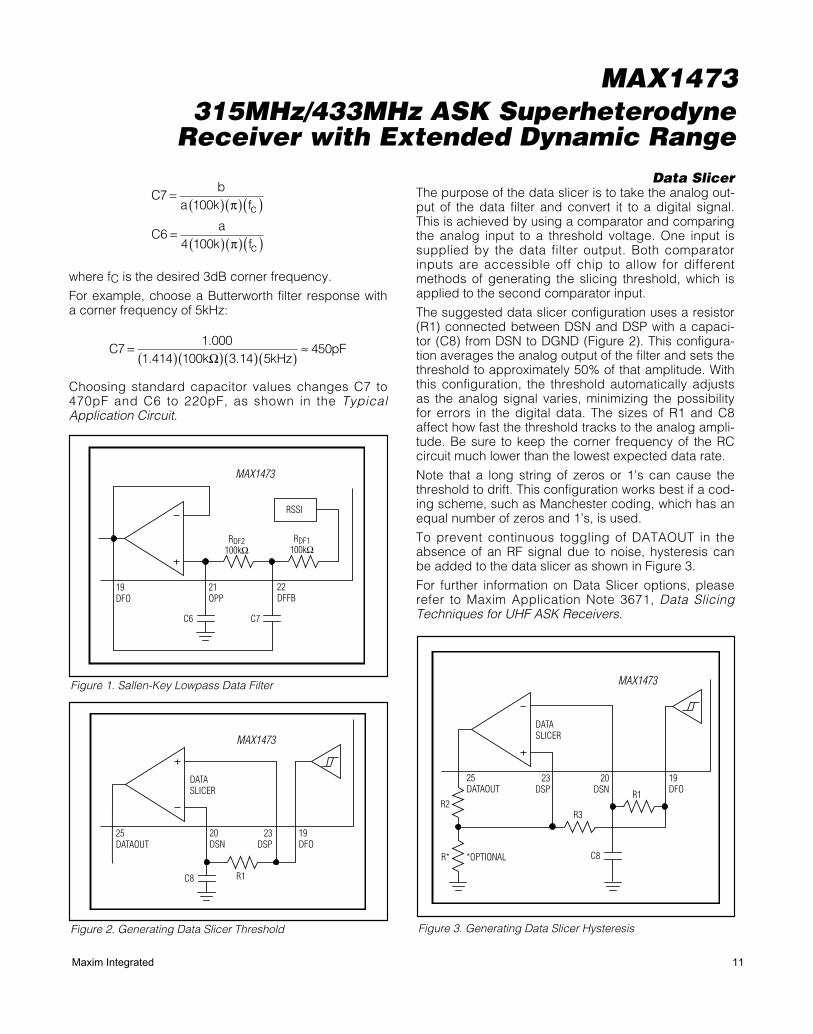
Data FilterThe data filter is implemented as a 2nd-order lowpassSallen-Key filter. The pole locations are set by the com-bination of two on-chip resistors and two externalcapacitors. Adjusting the value of the external capaci-tors changes the corner frequency to optimize for dif-ferent data rates. The corner frequency should be setto approximately 1.5 times the fastest expected datarate from the transmitter. Keeping the corner frequencynear the data rate rejects any noise at higher frequen-cies, resulting in an increase in receiver sensitivity.
The configuration shown in Figure 1 can create aButterworth or Bessel response. The Butterworth filteroffers a very flat amplitude response in the passbandand a rolloff rate of 40dB/decade for the two-pole filter.The Bessel filter has a linear phase response, whichworks well for filtering digital data. To calculate thevalue of C7 and C6, use the following equations alongwith the coefficients in Table 1:
fC
C C C Cp
m
case load case spec=
⎛
⎝⎜⎜
⎞
⎠⎟⎟
×+ +2
1 1106
-
Table 1. Coefficents to Calculate C7 and C6FILTER TYPE a b
Butterworth (Q = 0.707) 1.414 1.000
Bessel (Q = 0.577) 1.3617 0.618
MAX1473
10 Maxim Integrated
315MHz/433MHz ASK SuperheterodyneReceiver with Extended Dynamic Range
where fC is the desired 3dB corner frequency.
For example, choose a Butterworth filter response witha corner frequency of 5kHz:
Choosing standard capacitor values changes C7 to470pF and C6 to 220pF, as shown in the TypicalApplication Circuit.
Data SlicerThe purpose of the data slicer is to take the analog out-put of the data filter and convert it to a digital signal.This is achieved by using a comparator and comparingthe analog input to a threshold voltage. One input issupplied by the data filter output. Both comparatorinputs are accessible off chip to allow for differentmethods of generating the slicing threshold, which isapplied to the second comparator input.
The suggested data slicer configuration uses a resistor(R1) connected between DSN and DSP with a capaci-tor (C8) from DSN to DGND (Figure 2). This configura-tion averages the analog output of the filter and sets thethreshold to approximately 50% of that amplitude. Withthis configuration, the threshold automatically adjustsas the analog signal varies, minimizing the possibilityfor errors in the digital data. The sizes of R1 and C8affect how fast the threshold tracks to the analog ampli-tude. Be sure to keep the corner frequency of the RCcircuit much lower than the lowest expected data rate.
Note that a long string of zeros or 1’s can cause thethreshold to drift. This configuration works best if a cod-ing scheme, such as Manchester coding, which has anequal number of zeros and 1’s, is used.
To prevent continuous toggling of DATAOUT in theabsence of an RF signal due to noise, hysteresis canbe added to the data slicer as shown in Figure 3.
For further information on Data Slicer options, pleaserefer to Maxim Application Note 3671, Data SlicingTechniques for UHF ASK Receivers.
Ck kHz
pF71 000
1 414 100 3 14 5450
.. .
= ( ) ( ) ( ) ( ) ≈Ω
Cb
a k f
Ca
k f
c
c
7100
64 100
= ( ) ( ) ( )= ( ) ( ) ( )
π
π
RSSI
RDF1100kΩ
RDF2100kΩ
C7
19DFO
21OPP
22DFFB
C6
MAX1473
Figure 1. Sallen-Key Lowpass Data Filter
DATA SLICER
R1
25DATAOUT
20DSN
19DFO
23DSP
C8
MAX1473
Figure 2. Generating Data Slicer Threshold
DATA SLICER
R3R2
R*
R1
25DATAOUT
*OPTIONAL
23DSP
19DFO
20DSN
C8
MAX1473
Figure 3. Generating Data Slicer Hysteresis
MAX1473
Maxim Integrated 11
315MHz/433MHz ASK SuperheterodyneReceiver with Extended Dynamic Range
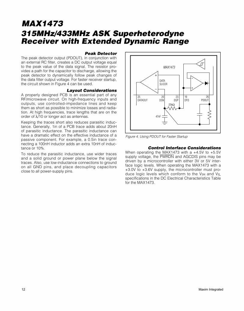
Peak DetectorThe peak detector output (PDOUT), in conjunction withan external RC filter, creates a DC output voltage equalto the peak value of the data signal. The resistor pro-vides a path for the capacitor to discharge, allowing thepeak detector to dynamically follow peak changes ofthe data filter output voltage. For faster receiver startup,the circuit shown in Figure 4 can be used.
Layout ConsiderationsA properly designed PCB is an essential part of anyRF/microwave circuit. On high-frequency inputs andoutputs, use controlled-impedance lines and keepthem as short as possible to minimize losses and radia-tion. At high frequencies, trace lengths that are on theorder of λ/10 or longer act as antennas.
Keeping the traces short also reduces parasitic induc-tance. Generally, 1in of a PCB trace adds about 20nHof parasitic inductance. The parasitic inductance canhave a dramatic effect on the effective inductance of apassive component. For example, a 0.5in trace con-necting a 100nH inductor adds an extra 10nH of induc-tance or 10%.
To reduce the parasitic inductance, use wider tracesand a solid ground or power plane below the signaltraces. Also, use low-inductance connections to groundon all GND pins, and place decoupling capacitorsclose to all power-supply pins.
Control Interface ConsiderationsWhen operating the MAX1473 with a +4.5V to +5.5Vsupply voltage, the PWRDN and AGCDIS pins may bedriven by a microcontroller with either 3V or 5V inter-face logic levels. When operating the MAX1473 with a+3.0V to +3.6V supply, the microcontroller must pro-duce logic levels which conform to the VIH and VILspecifications in the DC Electrical Characteristics Tablefor the MAX1473.
DATA SLICER
25kΩ
25DATAOUT
20DSN
19DFO
26PDOUT
23DSP
MAX1473
47nF
Figure 4. Using PDOUT for Faster Startup
MAX1473
12 Maxim Integrated
315MHz/433MHz ASK SuperheterodyneReceiver with Extended Dynamic Range
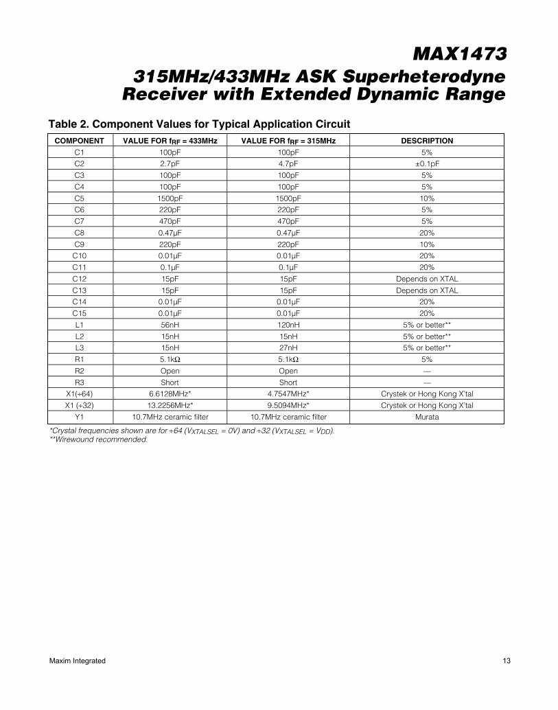
Table 2. Component Values for Typical Application CircuitCOMPONENT VALUE FOR fRF = 433MHz VALUE FOR fRF = 315MHz DESCRIPTION
C1 100pF 100pF 5%C2 2.7pF 4.7pF ±0.1pF
C3 100pF 100pF 5%
C4 100pF 100pF 5%
C5 1500pF 1500pF 10%C6 220pF 220pF 5%
C7 470pF 470pF 5%
C8 0.47µF 0.47µF 20%
C9 220pF 220pF 10%C10 0.01µF 0.01µF 20%
C11 0.1µF 0.1µF 20%
C12 15pF 15pF Depends on XTAL
C13 15pF 15pF Depends on XTALC14 0.01µF 0.01µF 20%
C15 0.01µF 0.01µF 20%
L1 56nH 120nH 5% or better**
L2 15nH 15nH 5% or better**L3 15nH 27nH 5% or better**
R1 5.1kΩ 5.1kΩ 5%
R2 Open Open —
R3 Short Short —X1(÷64) 6.6128MHz* 4.7547MHz* Crystek or Hong Kong X’tal
X1 (÷32) 13.2256MHz* 9.5094MHz* Crystek or Hong Kong X’tal
Y1 10.7MHz ceramic filter 10.7MHz ceramic filter Murata
*Crystal frequencies shown are for ÷64 (VXTALSEL = 0V) and ÷32 (VXTALSEL = VDD).**Wirewound recommended.
MAX1473
Maxim Integrated 13
315MHz/433MHz ASK SuperheterodyneReceiver with Extended Dynamic Range
Typical Application Circuit
28
C13
L1
C11
IF VDD IS
3.0V TO 3.6V
4.5V TO 5.5V
THEN VDD3 IS
CONNECTED TO VDD
CREATED BY LDO,AVAILABLE AT AVDD
(PIN 2)
C1
C2
L2
L3C3
C4
VDD3
RF INPUT
VDD3
VDD
C12
X1
27
26
25
24
23
22
21
20
19
18
17
16
15
1
2
3
4
5
6
7
8
9
10
11
12
13
14
MAX1473
DVDD
IF FILTER
COMPONENT VALUESIN TABLE 2
Y1
GNDIN OUT
DGND
MIXOUT
IRSEL
AGND
MIXIN2
MIXIN1
AVDD
LNAOUT
C9
** SEE MIXER SECTION * SEE PHASE-LOCKED LOOP SECTION
C10
AGND
LNASRC
LNAIN
AVDD
XTAL1 XTAL2TO/FROM µPPOWER DOWNDATA OUT
PWRDN
PDOUT
DATAOUT
VDD5
DSP
AGCDIS
DFFB
C8
R1
R2
R3
C7
C6C5
OPP
DSN
DFO
IFIN2
IFIN1
XTALSEL
C15
(SEE TABLE)
C14
**
*
FROM µP
Chip InformationPROCESS: CMOS
MAX1473
14 Maxim Integrated
315MHz/433MHz ASK SuperheterodyneReceiver with Extended Dynamic Range
PACKAGE TYPE PACKAGE CODE OUTLINE NO.LAND
PATTERN NO.
28 TSSOP U28+1 21-0066 90-0171
32 Thin QFN-EP T3255+3 21-0140 90-0001
Package InformationFor the latest package outline information and land patterns (footprints), go to www.maxim-ic.com/packages. Note that a “+”, “#”, or“-” in the package code indicates RoHS status only. Package drawings may show a different suffix character, but the drawing per-tains to the package regardless of RoHS status.
Functional Diagram
LNAOUT MIXIN1 MIXIN2
0˚
90˚
IFIN1MIXOUT IFIN2
RSSI
RDF2100kΩ
RDF1100kΩ
DIVIDEBY 64
VCO
LOOPFILTER
PHASEDETECTOR
CRYSTALDRIVER
POWERDOWN
IF LIMITINGAMPS
14
LNASRC
DATASLICER
DATAFILTER
Q∑
I
AUTOMATICGAIN
CONTROLIMAGE
REJECTION
3.2V REG24
2
IRSEL
13
5,10
AVDD
VDD5
DVDD
DGND
AGND
LNAIN3
XTALSEL
16
XTAL1
1
XTAL2
28
PWRDN
27
DATAOUT
25
DSN
20
DSP
23
DFO
19
PDOUT
26
OPP
21
DFFB
22
4 15 6 8 9 11 12 17 18AGCDIS
÷2÷1
MAX1473
LNA
7AVDD
MAX1473
Maxim Integrated 15
315MHz/433MHz ASK SuperheterodyneReceiver with Extended Dynamic Range
Revision History
REVISION NUMBER
REVISION DATE
DESCRIPTION PAGES
CHANGED
4 5/10 Added lead-free parts and exposed pad in Ordering Information and Pin Description tables
1, 8
5 1/11
Updated Absolute Maximum Ratings, AC Electrical Characteristics, Pin Description, Layout Considerations, Typical Application Circuit, Functional Diagram, and Package Information; added Voltage Regulator section to the Detailed Description section
2, 3, 4, 8, 9, 12, 13, 14
6 1/12 Updated DC Electrical and AC Electrical Characteristics tables, replaced TOC 4, updated Tables 1 and 2 and Figure 1; updated Phase-Locked Loop, Data Filter,Data Slicer, and Layout Considerations sections
3, 5, 6, 10–13
MAX1473
16 Maxim Integrated 160 Rio Robles, San Jose, CA 95134 USA 1-408-601-1000
Maxim cannot assume responsibility for use of any circuitry other than circuitry entirely embodied in a Maxim product. No circuit patent licenses are implied. Maxim reserves the right to change the circuitry and specifications without notice at any time. The parametric values (min and max limits) shown in the Electrical Characteristics table are guaranteed. Other parametric values quoted in this data sheet are provided for guidance.
© 2012 Maxim Integrated The Maxim logo and Maxim Integrated are trademarks of Maxim Integrated Products, Inc.