Embed Size (px)
DESCRIPTION
These are interesting slides for researchers and RF LNA IC's deign engineers. The slides includes the steps and equations of the design process.
Citation preview
Dr. Ahmed Bassyouni 1
Dr. Ahmed M. BassyouniDr. Ahmed M. Bassyouni Research ProfessorResearch Professor
Electrical and Computer Engineering DepartmentElectrical and Computer Engineering DepartmentBoise State University, IdahoBoise State University, Idaho
On-chip RF On-chip RF Transceiver CircuitsTransceiver Circuits
Dr. Ahmed Bassyouni 2
A Design Approach for Sub-micronCMOS Low Noise Amplifier
Electrical Engineering Department
Boise State University, Boise Idaho
Dr. Ahmed Bassyouni 3
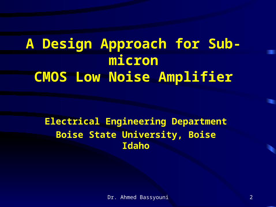
Receiver channel
Dr. Ahmed Bassyouni 4
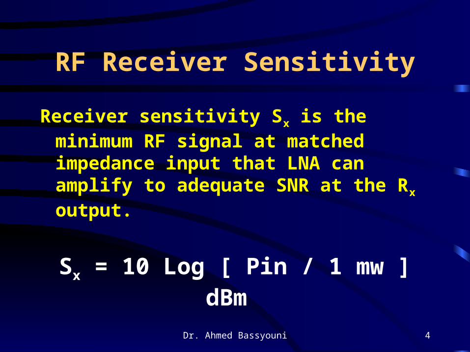
RF Receiver Sensitivity
Receiver sensitivity Sx is the minimum RF signal at matched impedance input that LNA can amplify to adequate SNR at the Rx output.
Sx = 10 Log [ Pin / 1 mw ] dBm
Dr. Ahmed Bassyouni 5
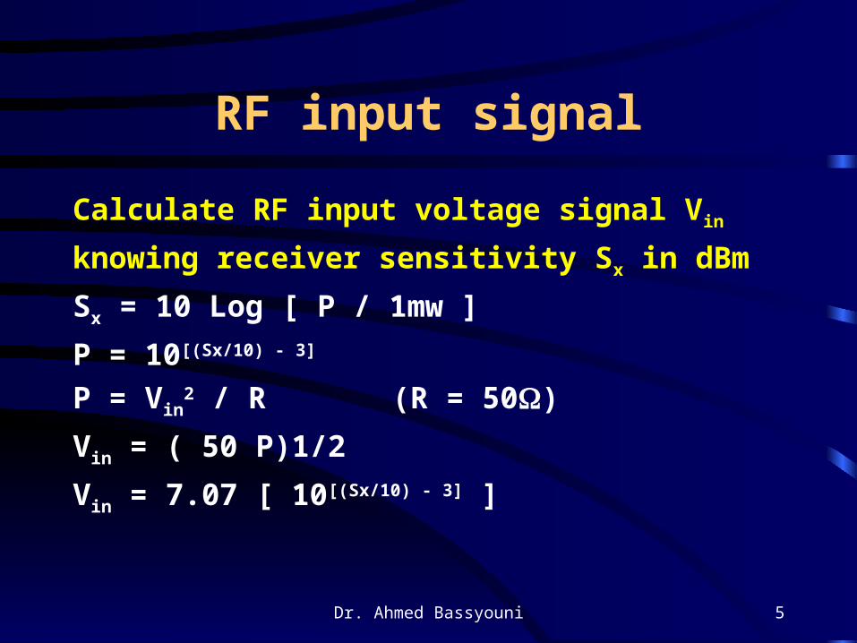
RF input signal
Calculate RF input voltage signal Vin
knowing receiver sensitivity Sx in dBm
Sx = 10 Log [ P / 1mw ]
P = 10[(Sx/10) - 3]
P = Vin2 / R (R = 50)
Vin = ( 50 P)1/2
Vin = 7.07 [ 10[(Sx/10) - 3] ]
Dr. Ahmed Bassyouni 6
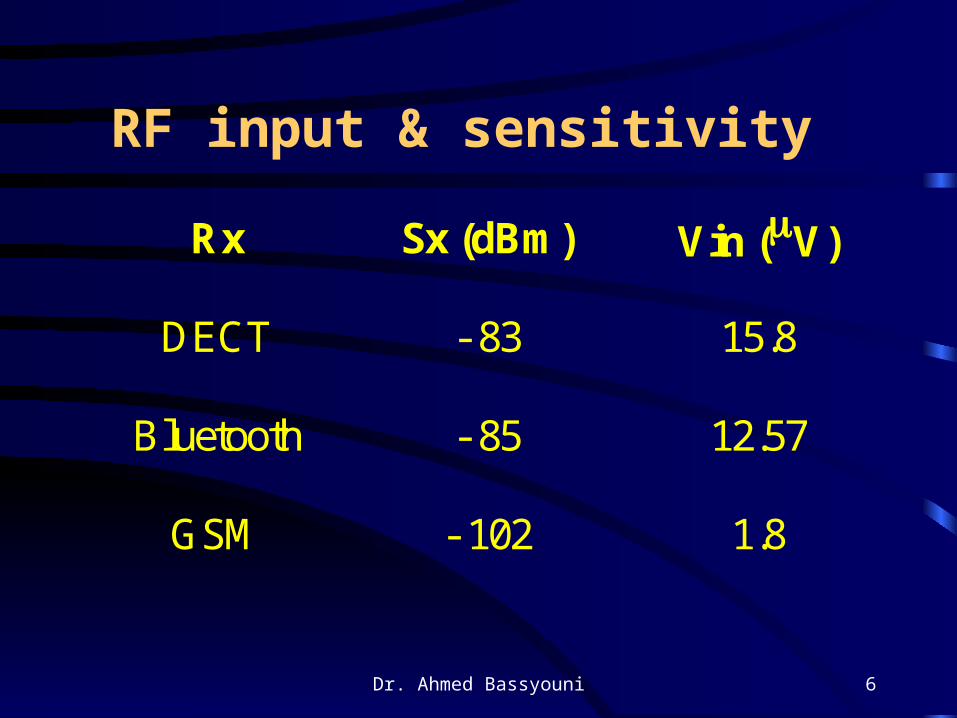
RF input & sensitivity
Rx Sx (dBm) Vin (V)
DECT - 83 15.8
Bluetooth - 85 12.57
GSM - 102 1.8
Dr. Ahmed Bassyouni 7
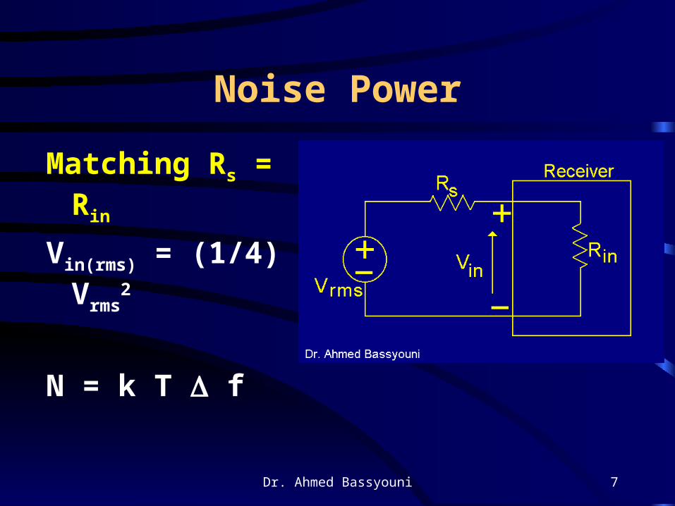
Noise Power
Matching Rs = Rin
Vin(rms) = (1/4) Vrms2
N = k T f
Dr. Ahmed Bassyouni 8
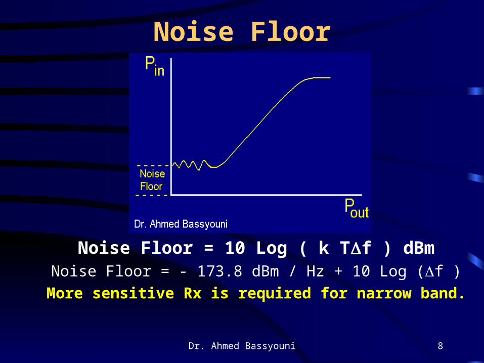
Noise Floor
Noise Floor = 10 Log ( k Tf ) dBmNoise Floor = - 173.8 dBm / Hz + 10 Log (f )
More sensitive Rx is required for narrow band.
Dr. Ahmed Bassyouni 9
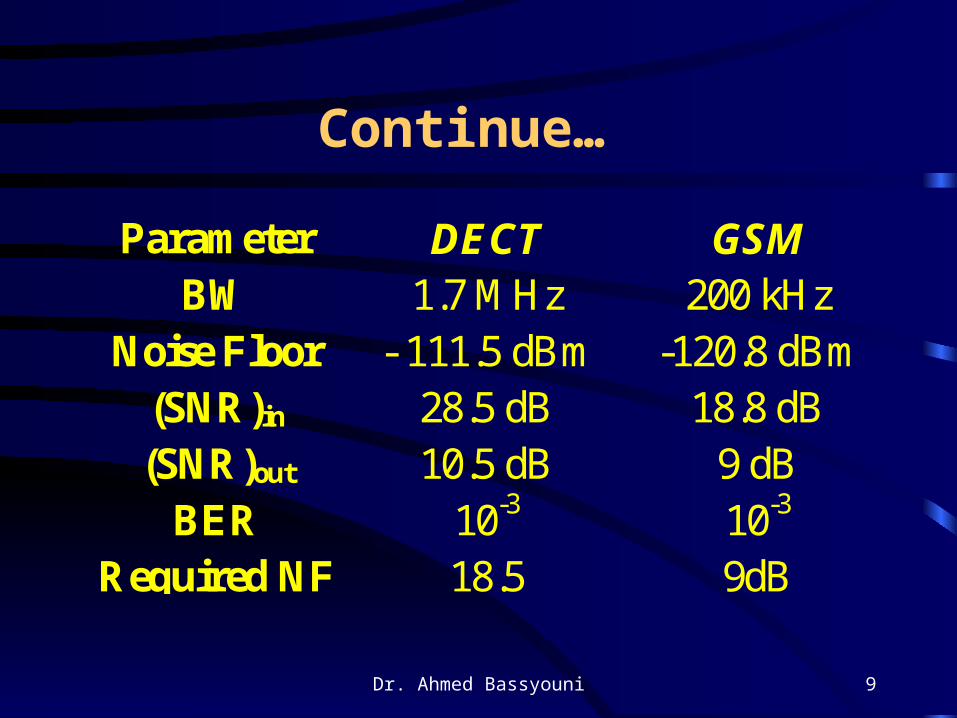
Continue…
Parameter DECT GSMBW 1.7 MHz 200 kHz
Noise Floor - 111.5 dBm -120.8 dBm(SNR)in 28.5 dB 18.8 dB(SNR)out 10.5 dB 9 dB
BER 10-3 10-3
Required NF 18.5 9dB
Dr. Ahmed Bassyouni 10
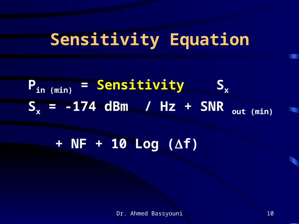
Sensitivity Equation
Pin (min) = Sensitivity Sx
Sx = -174 dBm / Hz + SNR out (min)
+ NF + 10 Log (f)
Dr. Ahmed Bassyouni 11
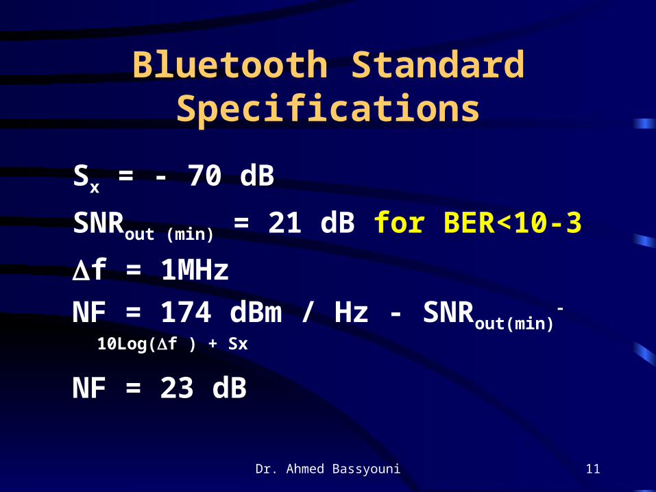
Bluetooth Standard Specifications
Sx = - 70 dB
SNRout (min) = 21 dB for BER<10-3
f = 1MHz
NF = 174 dBm / Hz - SNRout(min)-10Log(f ) + Sx
NF = 23 dB
Dr. Ahmed Bassyouni 12
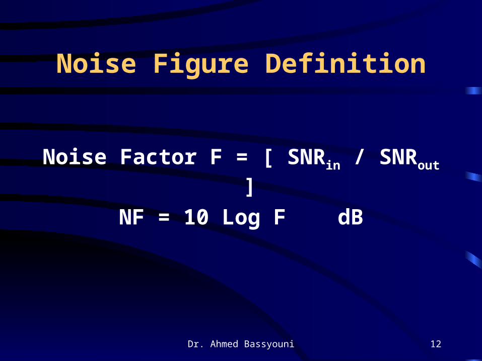
Noise Figure Definition
Noise Factor F = [ SNRin / SNRout ]
NF = 10 Log F dB
Dr. Ahmed Bassyouni 13
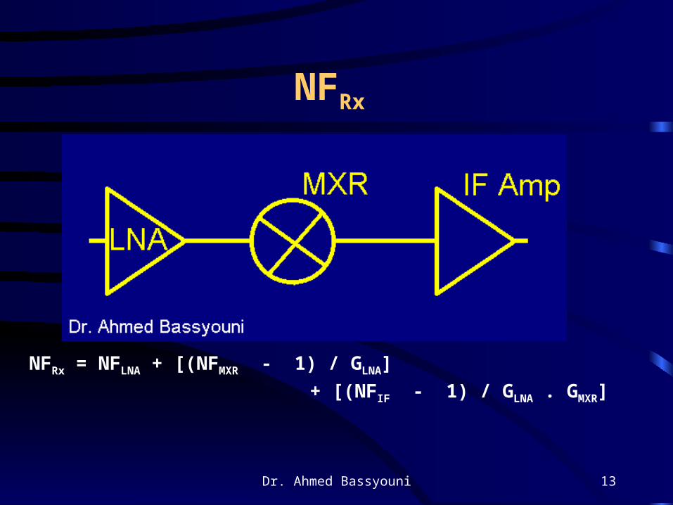
NFRx
NFRx = NFLNA + [(NFMXR - 1) / GLNA]
+ [(NFIF - 1) / GLNA . GMXR]
Dr. Ahmed Bassyouni 14
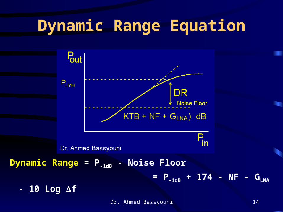
Dynamic Range Equation
Dynamic Range = P-1dB - Noise Floor
= P-1dB + 174 - NF - GLNA - 10 Log f
Dr. Ahmed Bassyouni 15
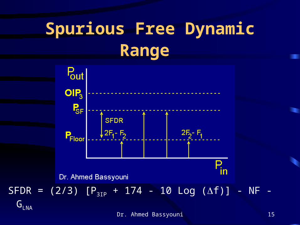
Spurious Free Dynamic Range
SFDR = (2/3) [P3IP + 174 - 10 Log (f)] - NF -GLNA
Dr. Ahmed Bassyouni 16
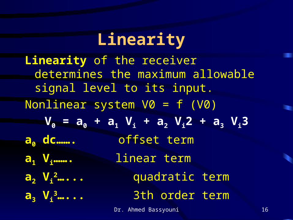
Linearity Linearity of the receiver determines the
maximum allowable signal level to its input.
Nonlinear system V0 = f (V0)
V0 = a0 + a1 Vi + a2 Vi2 + a3 Vi3
a0 dc……. offset term
a1 Vi……. linear term
a2 Vi2…... quadratic term
a3 Vi3…... 3th order term
Dr. Ahmed Bassyouni 17
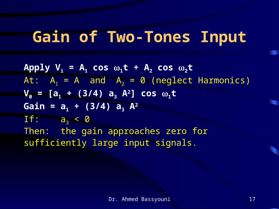
Gain of Two-Tones Input
Apply Vi = A1 cos 1t + A2 cos 2t
At: A1 = A and A2 = 0 (neglect Harmonics)
V0 = [a1 + (3/4) a3 A2] cos 1t
Gain = a1 + (3/4) a3 A2
If: a3 < 0Then: the gain approaches zero for sufficiently large input signals.
Dr. Ahmed Bassyouni 18
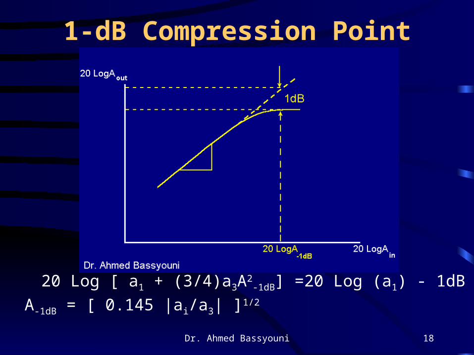
1-dB Compression Point
20 Log [ a1 + (3/4)a3A2-1dB] =20 Log (a1) - 1dB
A-1dB = [ 0.145 |ai/a3| ]1/2
Dr. Ahmed Bassyouni 19
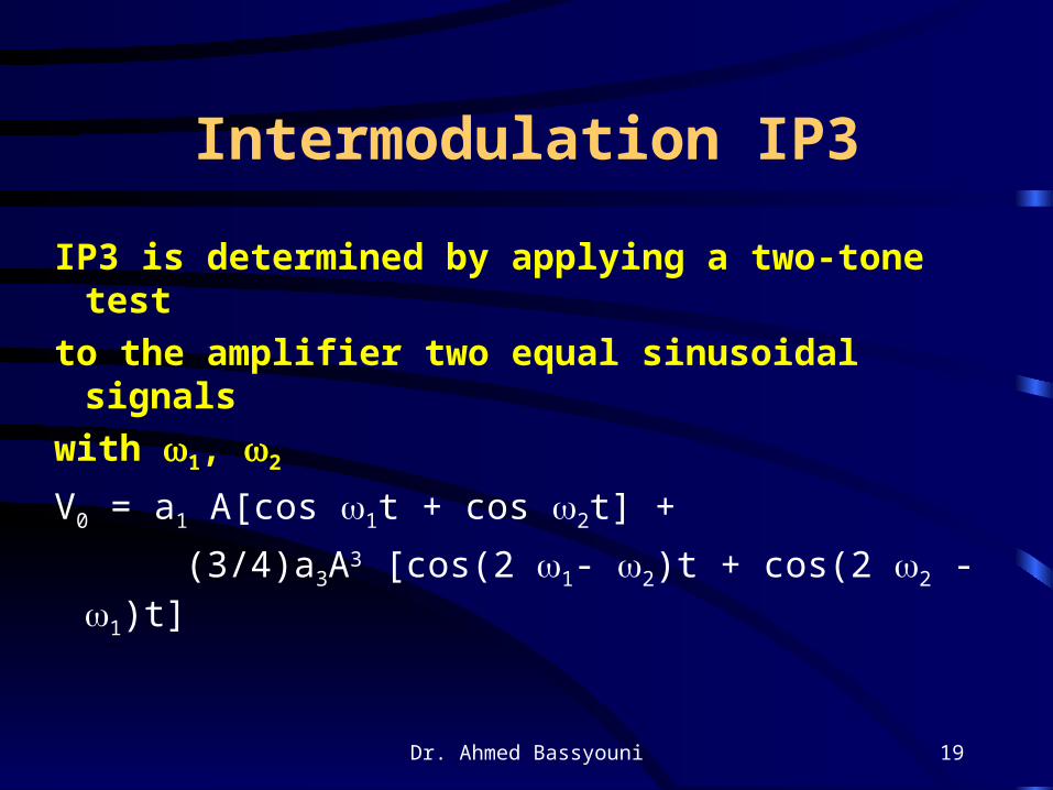
Intermodulation IP3
IP3 is determined by applying a two-tone test
to the amplifier two equal sinusoidal signals
with 1, 2
V0 = a1 A[cos 1t + cos 2t] +
(3/4)a3A3 [cos(2 1- 2)t + cos(2 2 - 1)t]
Dr. Ahmed Bassyouni 20
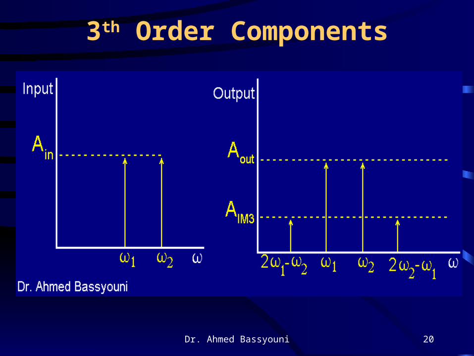
3th Order Components
Dr. Ahmed Bassyouni 21
OIP3:3rd order of Distortion
The theoretical output level where 3th
order distortion components
(21 - 2) & (2 2 - 1) equal
the desired output signal level is called
the 3th order output intercept.
Dr. Ahmed Bassyouni 22
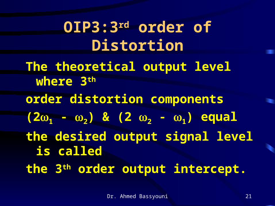
Distortion Condition
OIP3, IIP3: 3rd order output, and input intercept.
Distortion occurs at the applied input level
Ain = IIP3 a1 AIIP3 = (3/4) a3 A3IIP3
AIIP3 = [(3/4) |a1/a3|]
Dr. Ahmed Bassyouni 23
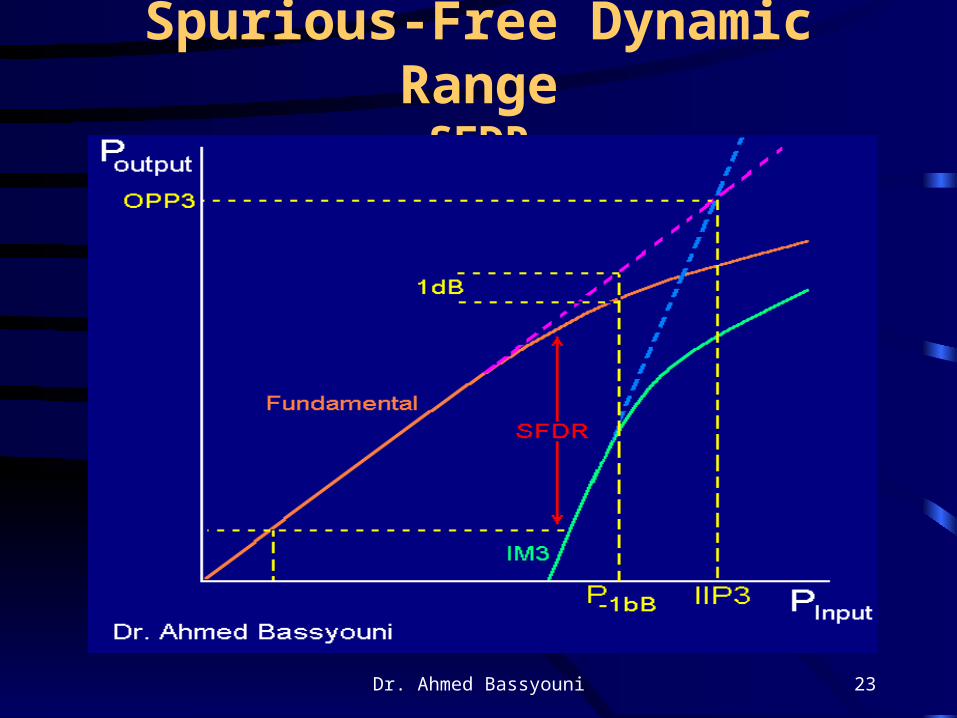
Spurious-Free Dynamic RangeSFDR
Dr. Ahmed Bassyouni 24
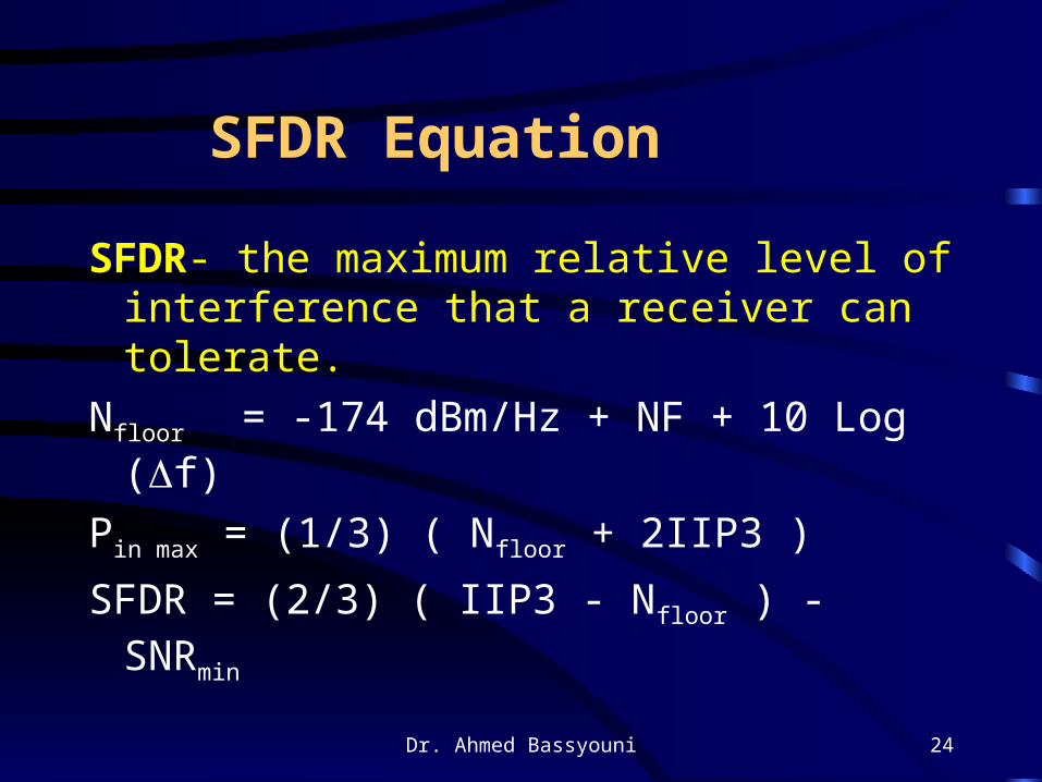
SFDR Equation
SFDR- the maximum relative level of interference that a receiver can tolerate.
Nfloor = -174 dBm/Hz + NF + 10 Log (f)
Pin max = (1/3) ( Nfloor + 2IIP3 )
SFDR = (2/3) ( IIP3 - Nfloor ) - SNRmin
Dr. Ahmed Bassyouni 25
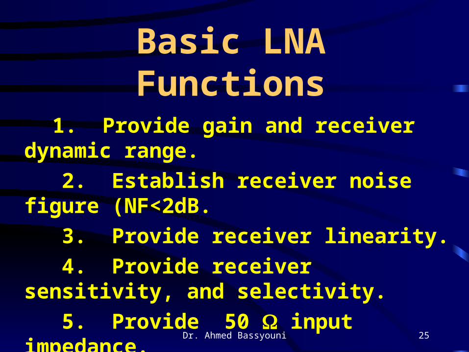
Basic LNA Functions
1. Provide gain and receiver dynamic range.
2. Establish receiver noise figure (NF<2dB.
3. Provide receiver linearity.
4. Provide receiver sensitivity, and selectivity.
5. Provide 50 input impedance.
6. Minimum power dissipation.
7. Provide receiver stability.
Dr. Ahmed Bassyouni 26
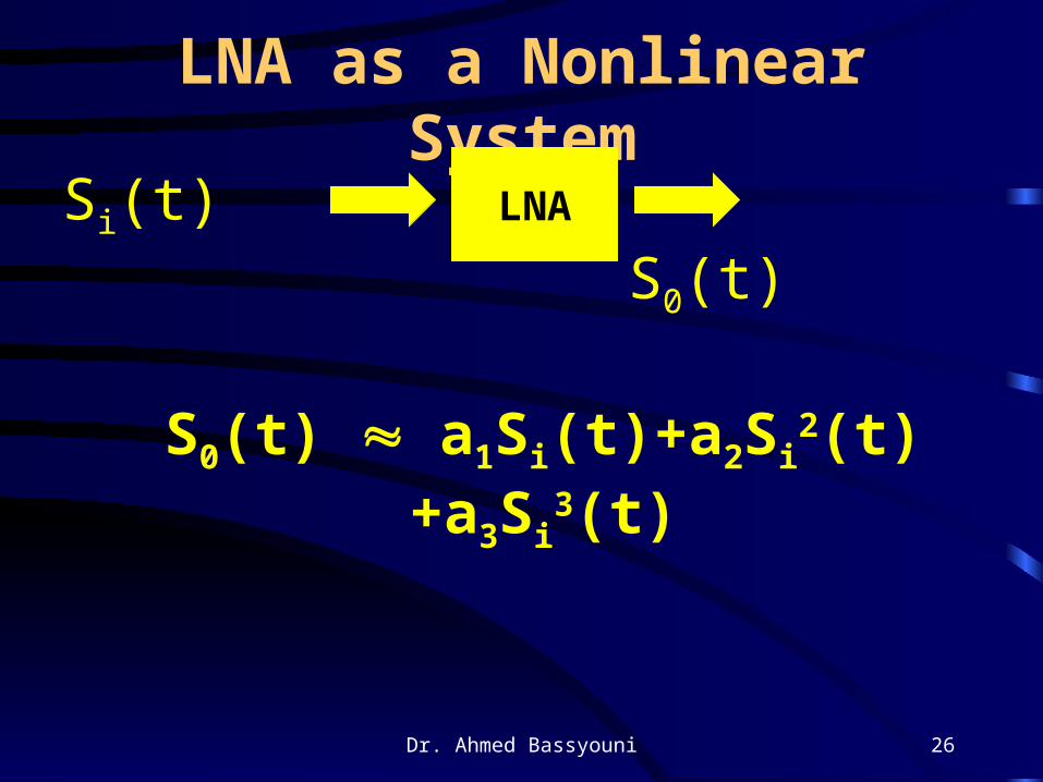
LNA as a Nonlinear System
Si(t) S0(t)
S0(t) a1Si(t)+a2Si2(t)+a3Si
3(t)
LNA
Dr. Ahmed Bassyouni 27
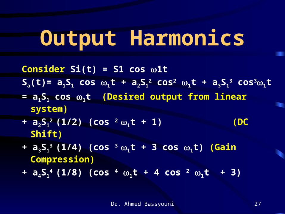
Output HarmonicsConsider Si(t) = S1 cos 1t
Sa(t)= a1S1 cos 1t + a2S12 cos2 1t + a3S1
3 cos31t
= a1S1 cos 1t (Desired output from linear system)
+ a2S12 (1/2) (cos 2 1t + 1) (DC Shift)
+ a3S13 (1/4) (cos 3 1t + 3 cos 1t) (Gain Compression)
+ a4S14 (1/8) (cos 4 1t + 4 cos 2 1t + 3)
Dr. Ahmed Bassyouni 28
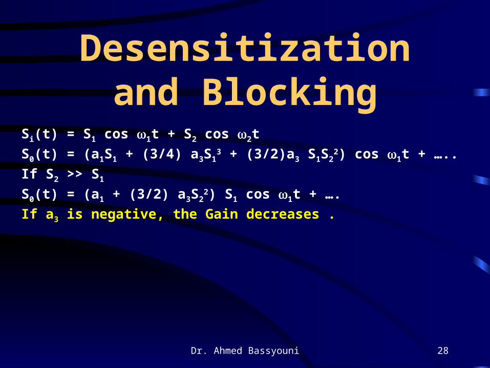
Desensitization and Blocking
Si(t) = S1 cos 1t + S2 cos 2t
S0(t) = (a1S1 + (3/4) a3S13 + (3/2)a3 S1S2
2) cos 1t + …..
If S2 >> S1
S0(t) = (a1 + (3/2) a3S22) S1 cos 1t + ….
If a3 is negative, the Gain decreases .
Dr. Ahmed Bassyouni 29
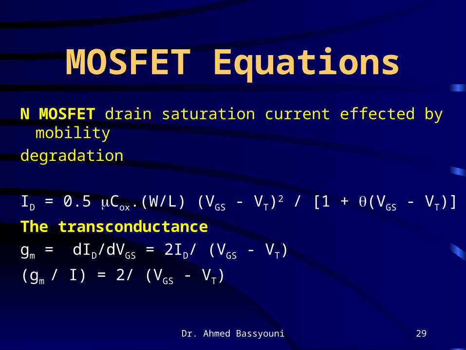
MOSFET EquationsN MOSFET drain saturation current effected by mobility
degradation
ID = 0.5 Cox.(W/L) (VGS - VT)2 / [1 + (VGS - VT)]
The transconductance
gm = dID/dVGS = 2ID/ (VGS - VT)
(gm / I) = 2/ (VGS - VT)
Dr. Ahmed Bassyouni 30
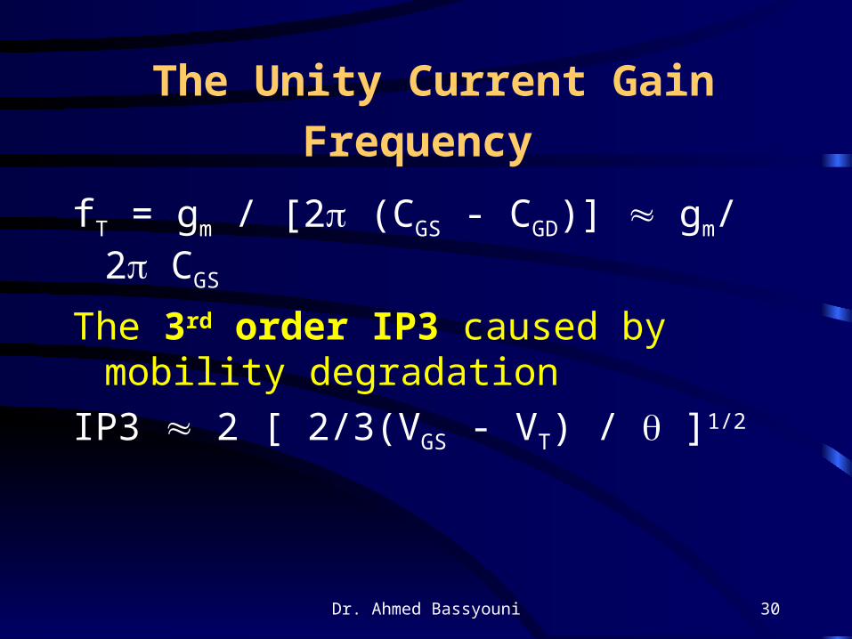
The Unity Current Gain Frequency
fT = gm / [2 (CGS - CGD)] gm/ 2 CGS
The 3rd order IP3 caused by mobility degradation
IP3 2 [ 2/3(VGS - VT) / ]1/2
Dr. Ahmed Bassyouni 31
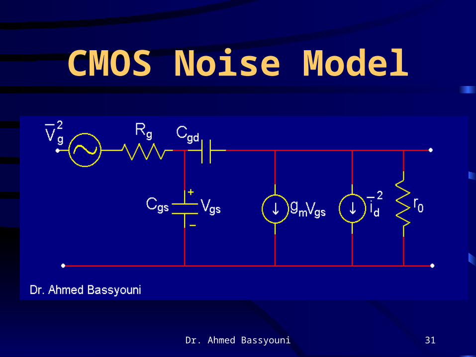
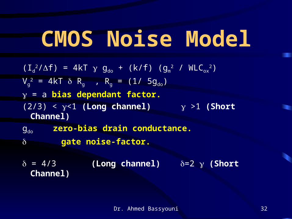
CMOS Noise Model
Dr. Ahmed Bassyouni 32
CMOS Noise Model(Id
2/f) = 4kT gdo + (k/f) (gm2 / WLCox
2)
Vg2 = 4kT Rg , Rg = (1/ 5gdo)
= a bias dependant factor.
(2/3) < <1 (Long channel) >1 (Short Channel)
gdo zero-bias drain conductance.
gate noise-factor.
= 4/3 (Long channel) =2 (Short Channel)
Dr. Ahmed Bassyouni 33
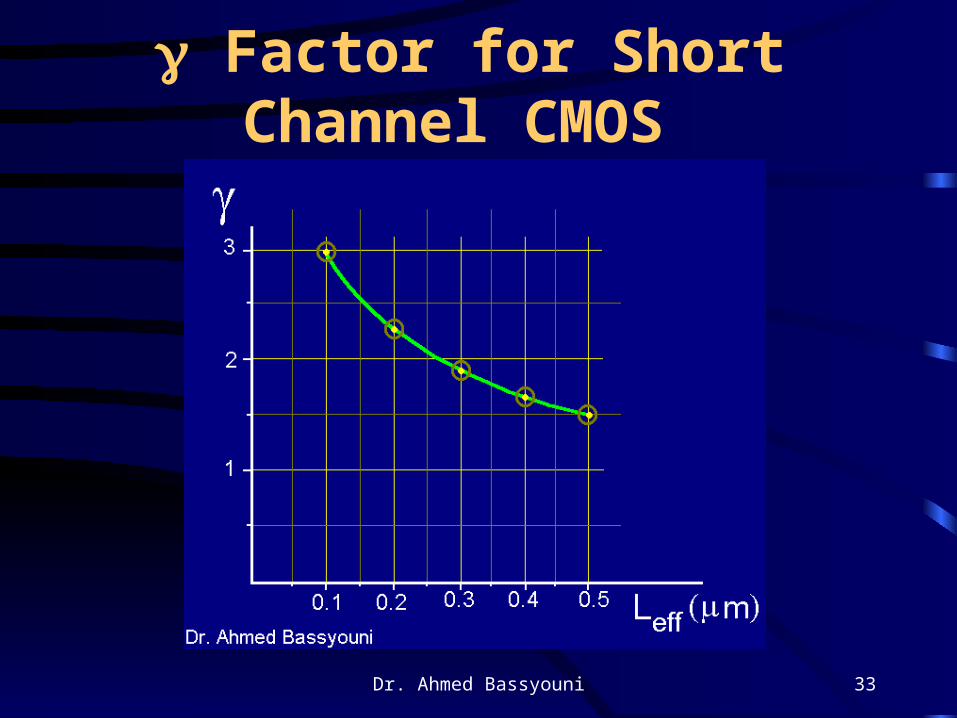
Factor for Short Channel CMOS
Dr. Ahmed Bassyouni 34
LNA Design Considerations
• The Gain is typically 10 dB < Gain <10 dB Sufficient gain to minimize
the influence of noise, but not too
high, otherwise interfering signals will exceed mixer’s linearity.
• NF must be as little as possible, up to the application. Bluetooth NF < 4 dB.
• Good linearity to accommodate large signals without distraction.
• Zin = 50 to ensure high quality gain-frequency for narrow band.
• Minimum power dissipation (can be achieved with scaled CMOS).
Dr. Ahmed Bassyouni 35
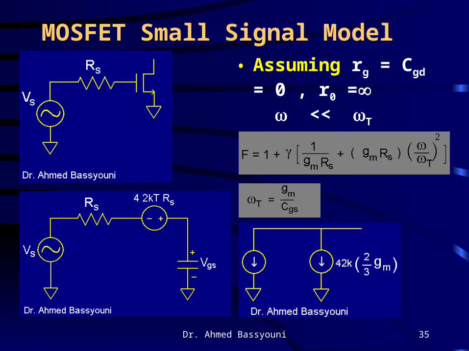
MOSFET Small Signal Model • Assuming rg = Cgd = 0 ,
r0 = << T
• Noise Factor
Dr. Ahmed Bassyouni 36
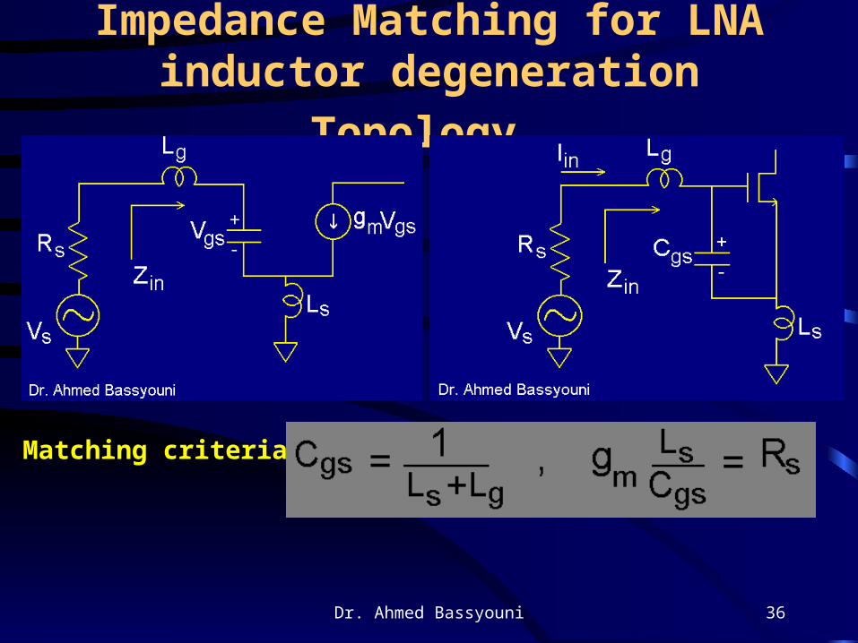
Impedance Matching for LNA
inductor degeneration Topology
Matching criteria
Dr. Ahmed Bassyouni 37
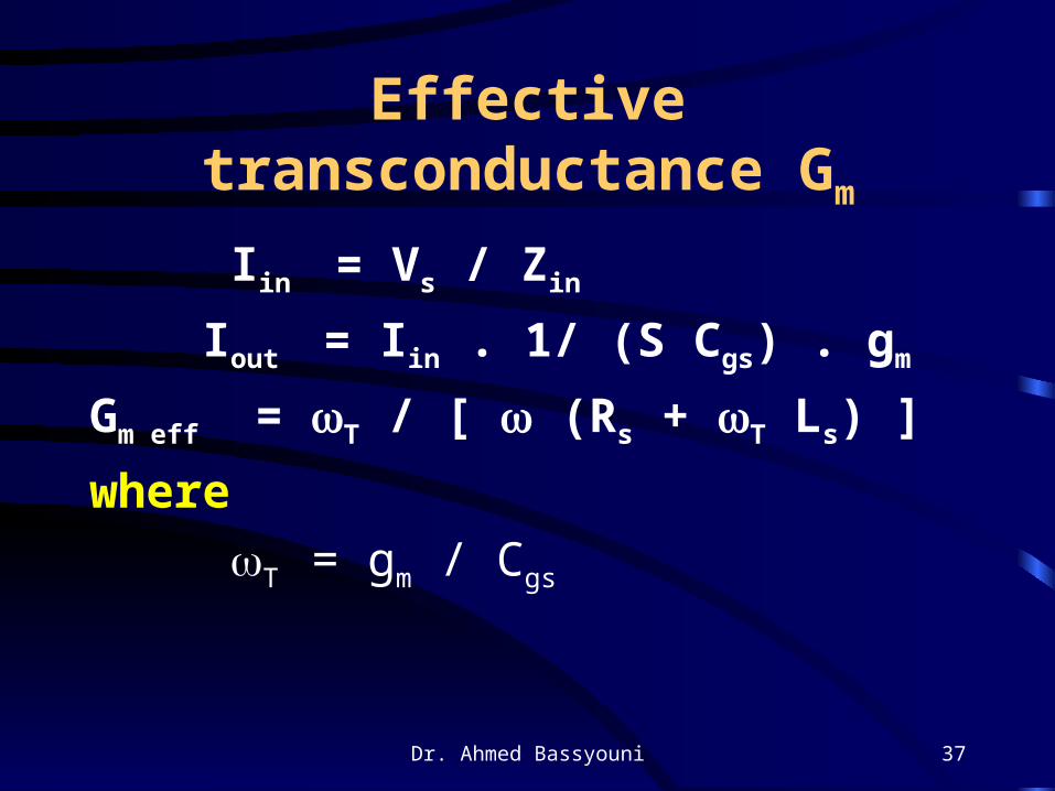
Effective transconductance Gm
Iin = Vs / Zin
Iout = Iin . 1/ (S Cgs) . gm
Gm eff = T / [ (Rs + T Ls) ]
where
T = gm / Cgs
Dr. Ahmed Bassyouni 38
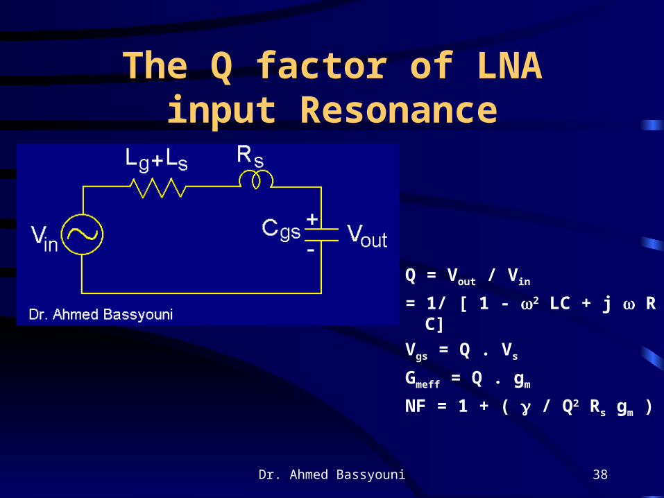
The Q factor of LNA input Resonance
Q = Vout / Vin
= 1/ [ 1 - 2 LC + j R C]
Vgs = Q . Vs
Gmeff = Q . gm
NF = 1 + ( / Q2 Rs gm )
Dr. Ahmed Bassyouni 39
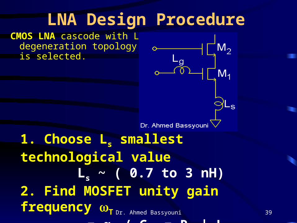
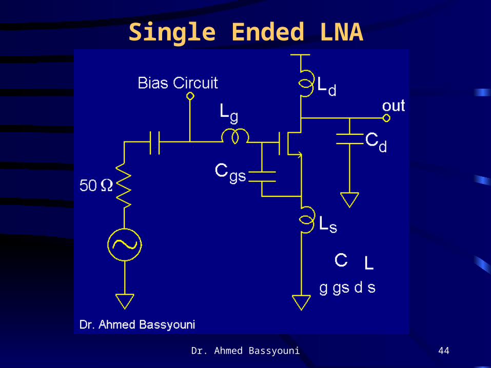
LNA Design ProcedureCMOS LNA cascode with
L degeneration topology is selected.
1. Choose Ls smallest technological value Ls ~ ( 0.7 to 3 nH)
2. Find MOSFET unity gain frequency T
T = gm / Cgs = Rs | Ls
Dr. Ahmed Bassyouni 40
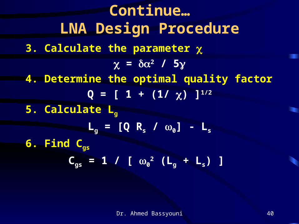
Continue…LNA Design Procedure
3. Calculate the parameter = 2 / 5
4. Determine the optimal quality factor
Q = [ 1 + (1/ ) ]1/2
5. Calculate Lg
Lg = [Q Rs / 0] - Ls
6. Find Cgs
Cgs = 1 / [ 02 (Lg + Ls) ]
Dr. Ahmed Bassyouni 41
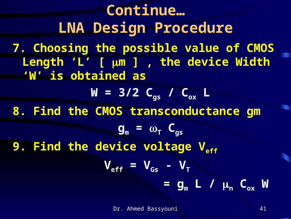
Continue…LNA Design Procedure
7. Choosing the possible value of CMOS Length ‘L’ [ m ] , the device Width ‘W’ is obtained as
W = 3/2 Cgs / Cox L
8. Find the CMOS transconductance gm
gm = T Cgs
9. Find the device voltage Veff
Veff = VGs - VT
= gm L / n Cox W
Dr. Ahmed Bassyouni 42
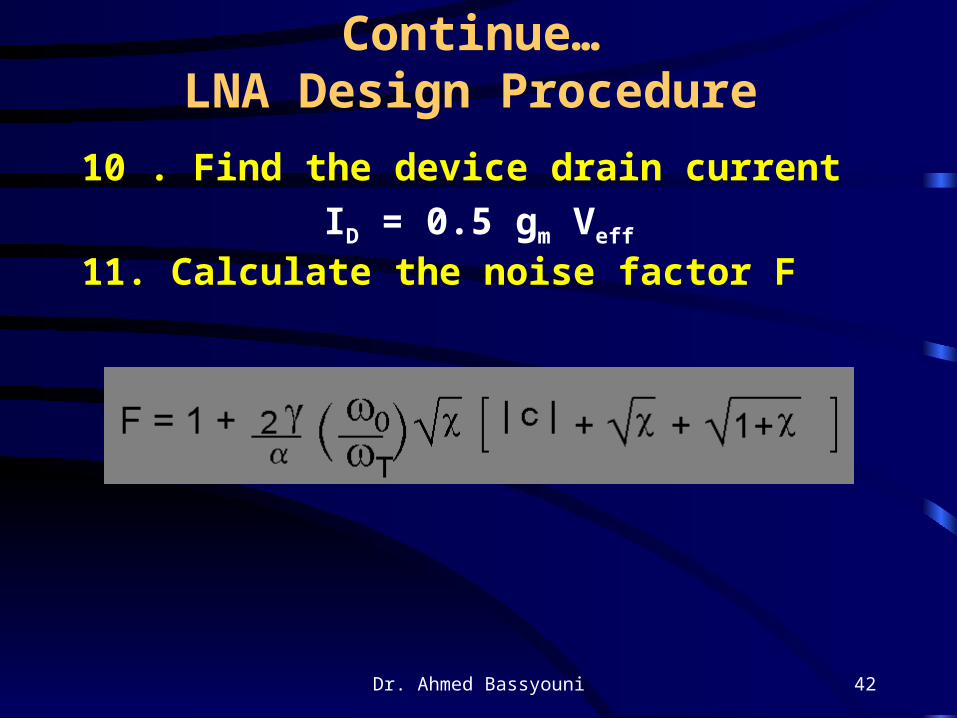
Continue…LNA Design Procedure
10 . Find the device drain current
ID = 0.5 gm Veff
11. Calculate the noise factor F
Dr. Ahmed Bassyouni 43
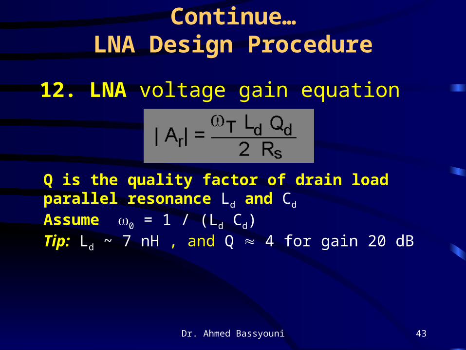
Continue…LNA Design Procedure
12. LNA voltage gain equation
Q is the quality factor of drain load parallel resonance Ld and Cd
Assume 0 = 1 / (Ld Cd)Tip: Ld ~ 7 nH , and Q 4 for gain 20 dB
Dr. Ahmed Bassyouni 44
Single Ended LNA
Dr. Ahmed Bassyouni 45
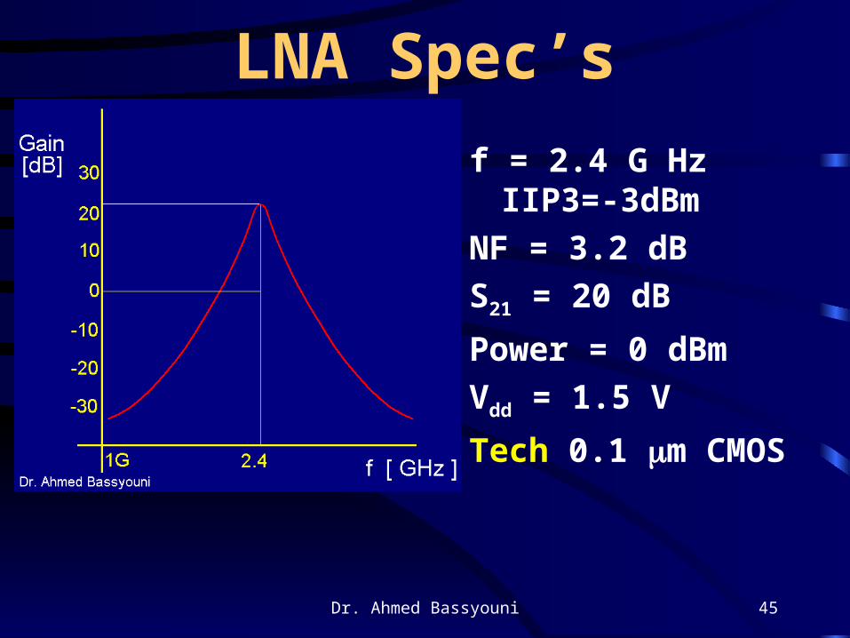
LNA Spec’s
f = 2.4 G Hz IIP3=-3dBm
NF = 3.2 dB
S21 = 20 dB
Power = 0 dBm
Vdd = 1.5 V
Tech 0.1 m CMOS


![&KDUDFWHUL]DWLRQ DQG &RPPLVVLRQLQJ RI D .D %DQG … · 2020-02-13 · Exp Sens ort SSPA LNA LNA WAVEGUIDE COAX Coupled Ports 20 dB 10 dB dB dB Fig. 1. CADeT RF Topology Diagram [1]](https://img.pdfslide.us/doc/110x75/5e97fe752ea1c604d6597052/kdudfwhuldwlrq-dqg-rpplvvlrqlqj-ri-d-d-dqg-2020-02-13-exp-sens-ort.jpg)


![RF Circuit Design - [Ch4-2] LNA, PA, and Broadband Amplifier](https://img.pdfslide.us/doc/110x75/55cf04aebb61eb002d8b45b4/rf-circuit-design-ch4-2-lna-pa-and-broadband-amplifier.jpg)