Embed Size (px)
Citation preview

Using Hermetic Optocouplers in Military and Space Electronics
White Paper
By Jamshed N. Khan Optocoupler Applications Engineer
AbstractSensitive and high reliability electronic applications in areas such as space, aeronautics, military, and naval envi-ronments will continue to rely on high reliability hermetic components. The risks associated with using plastic elec-tronic components in harsh and rugged environments, where components may be subjected to extremes of temperature, humidity, radiation, and shock/accelera-tion are just too great. Optically isolated (optocoupler/optoisolator) technology to provide noise-free data trans-mission and safe galvanic isolation has been around for over twenty years. The latest advances in the design and processing of transmitter and receiver technologies have enabled greater functionality, integration, and sophistica-tion of hermetic optocouplers for various electronic de-sign and application purposes. Hermetic optocouplers are now available for high speed digital data transmission ap-plications, analog optocouplers for sensing voltages and current, Intelligent Power Module (IPM) drivers for motor control applications, and AC/DC threshold voltage detec-tors for various high power detection purposes. Also avail-able are hermetic power MOSFET optocouplers (Avago Technologies’ HSSR-7111) for switching applications. To satisfy many types of end applications, these high reli-ability hermetic optocouplers are available as commer-cial grade, Class H (high reliability) and Class K (highest reliability). Most product families are available in various package styles (8 and 16 pin DIP, 16 lead Flat Pack, and 20 terminal LCC) and lead configurations for through-hole and surface mount applications.
Why Use Hermetic Optocouplers?Safe optical isolation using optocouplers or optoisolators is now a well-proven, well-established, and most reliable technology. Modern state-of-the-art optocouplers are available for high-speed digital data transmission applica-tions (up to 20 Mbit/s), analog current and voltage sens-ing, and feedback and control electronics. Application-specific optocouplers are also available for inverter (IGBT/MOSFET, and IPM) gate drivers, and AC/DC high voltage threshold sensing requirements.
Traditionally, optocouplers have been extensively used to safely isolate low power, delicate, and expensive elec-tronic components from high power circuits. In addition, optocouplers provide an excellent means of interfacing circuits with high ground potential differences, protecting circuits from large common mode voltages, and eliminat-ing noise and interference due to undesirable ground loop currents. Optocouplers are also used to provide amplifica-tion of signals, provide ON/OFF switching, and insulate hu-mans from electric shock and the hazards of high voltage power sources, as well as protect patients from high power medical instruments. Advances in optocoupler design and processing technologies have allowed new optocoupler designs for application-specific areas, as well as provided increasing functionality and sophistication.
Historically, digital data transmission applications were the first to realize the common mode noise elimination and surge protection benefits of optocouplers. Today, variable speed motor control electronics is one area where optocouplers are finding increasing applications. Also available are optocouplers optimized to provide high output sourcing and sinking capabilities to drive inverters (IGBTs / MOSFETs) or IPMs. Similarly, sophisticated analog optoisolators are increasingly replacing Hall Effect sensors for measuring and monitoring AC phase currents, DC rail/bus currents, and measuring bus voltages or monitoring temperatures.

2
Hermetic optocouplers are beneficial in wide temperature range (–55 to +125°C) applications, high humidity condi-tions as found in naval and marine environments, and where parts are invariably subjected to high mechanical shock such as aeronautics or satellites, and adverse radia-tion conditions such as space. The primary benefits of us-ing hermetic optocouplers can be summarized as follows:
• High reliability, high quality, and long life
• Variable speed and frequency capability
• Ease and simplicity of design
• Relatively small size and footprint area
• Relatively low power dissipation
• Safe optical isolation (galvanic isolation)
• Rugged—can withstand thermal or mechanical shocks
• Immunity to ground loop current noise interference
• Higher temperature operation
• Radiation tolerance for space applications
• Isolate different voltage levels and level shifting
• Amplify or attenuate digital or analog signals
• Insulate human operators from power circuits and shock hazards
• Prevent noise or interference between control and power circuits
• Provide high voltage transient protection for expensive digital circuits
Digital Applications of Hermetic OptocouplersModern communication relies on transmitting digital data. Technologies such as computers, satellites, telem-etry, electronics, and integrated circuits have paved the way for generating and transmitting enormous amounts of data. Figure 1 shows the basic elements of an optocou-pler-isolated transmission system and consists of opto-couplers, a transmitter or line driver, a transmission line or medium, receiver, and digital control logic at either end.
Note: Zcm represents the impedance associated with the source of the common mode interference and eCM repre-sents Common Mode Voltage.
The ground loop currents circulating between the two grounds of the transmission line often induce offsets and noise degradation of the integrity of the data. The use of the optocoupler as shown in Figure 1 breaks this ground loop current between the transmission line and the con-trol logic, which is often the CPU of a remote computer. The common mode interference associated with shifts in the ground potentials is another problem. Both of these effects, ground loop currents and common mode noise, can be eliminated when using optocouplers.
A common misunderstanding regarding optocouplers in digital data transmission applications is that optocouplers can be used directly either as line drivers or as line receiv-ers. Generally speaking, the optocoupler’s input stages or the output stages are TTL and/or CMOS logic compatible. These stages are not optimized to function directly as line receivers or line drivers. Although, with a careful under-standing of the digital data transmission standard and careful design of the optocoupler drive circuitry, in some cases, optocouplers can be made to act as line receivers. Invariably, optocouplers cannot drive the transmission line directly, as the output stages do not have the power capability to do so. For a safe and optimum design, it is highly recommended that a designer use an appropriate transceiver of the transmission standard under consider-ation in conjunction with the right optocoupler.
Figure 1. Basic Optically Isolated Transmission Line
Logic Optocoupler Isolation
Line Driver
Transmission Line
Line Receiver
GND 1 GND 2
OptocouplerIsolation
Zcm eCM
LogicLogic Optocoupler Isolation
Line Driver
Transmission Line
Line Receiver
optical isolation
GND 2
OptocouplerIsolation
Zcm eCM optical isolation
Isolated GND forModule 1
Isolated GND forModule 2
3
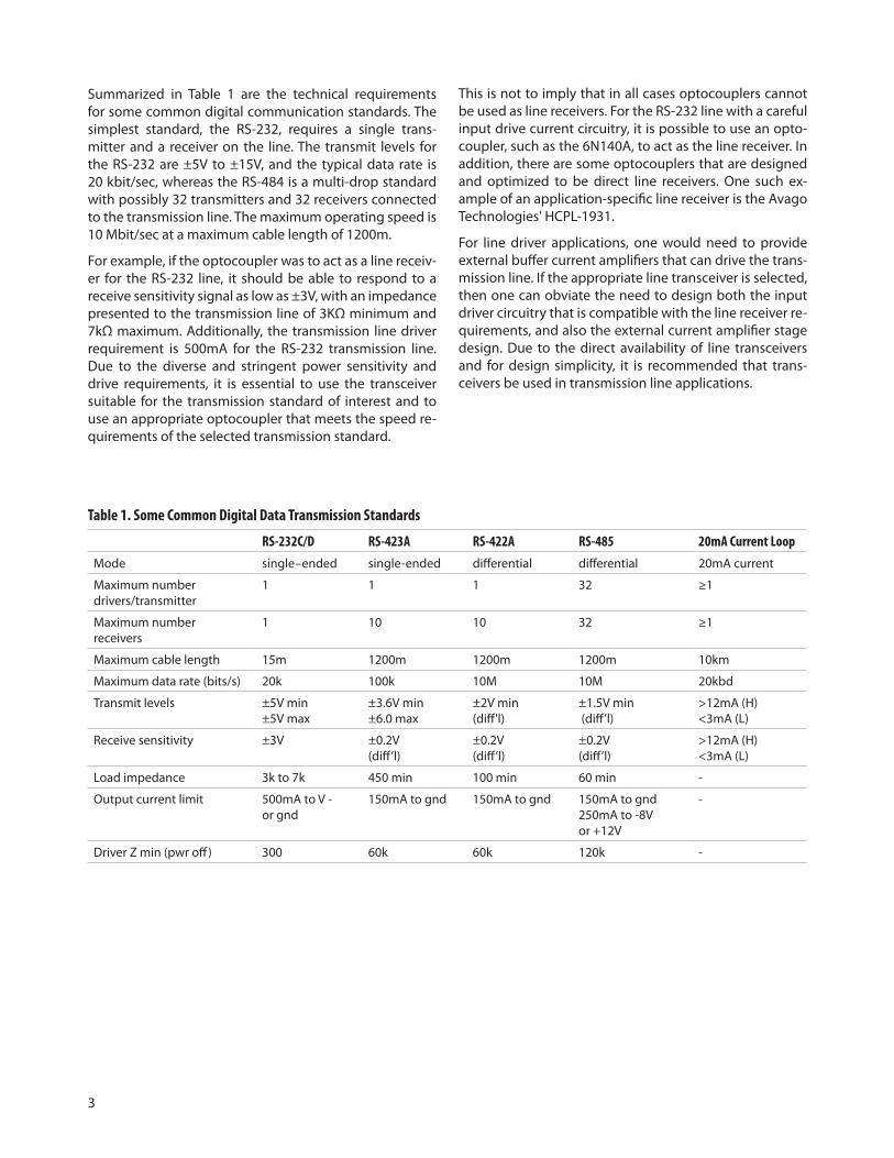
Summarized in Table 1 are the technical requirements for some common digital communication standards. The simplest standard, the RS-232, requires a single trans-mitter and a receiver on the line. The transmit levels for the RS-232 are ±5V to ±15V, and the typical data rate is 20 kbit/sec, whereas the RS-484 is a multi-drop standard with possibly 32 transmitters and 32 receivers connected to the transmission line. The maximum operating speed is 10 Mbit/sec at a maximum cable length of 1200m.
For example, if the optocoupler was to act as a line receiv-er for the RS-232 line, it should be able to respond to a receive sensitivity signal as low as ±3V, with an impedance presented to the transmission line of 3KΩ minimum and 7kΩ maximum. Additionally, the transmission line driver requirement is 500mA for the RS-232 transmission line. Due to the diverse and stringent power sensitivity and drive requirements, it is essential to use the transceiver suitable for the transmission standard of interest and to use an appropriate optocoupler that meets the speed re-quirements of the selected transmission standard.
This is not to imply that in all cases optocouplers cannot be used as line receivers. For the RS-232 line with a careful input drive current circuitry, it is possible to use an opto-coupler, such as the 6N140A, to act as the line receiver. In addition, there are some optocouplers that are designed and optimized to be direct line receivers. One such ex-ample of an application-specific line receiver is the Avago Technologies' HCPL-1931.
For line driver applications, one would need to provide external buffer current amplifiers that can drive the trans-mission line. If the appropriate line transceiver is selected, then one can obviate the need to design both the input driver circuitry that is compatible with the line receiver re-quirements, and also the external current amplifier stage design. Due to the direct availability of line transceivers and for design simplicity, it is recommended that trans-ceivers be used in transmission line applications.
Table 1. Some Common Digital Data Transmission Standards
RS-232C/D RS-423A RS-422A RS-485 20mA Current LoopMode single–ended single-ended differential differential 20mA current
Maximum number drivers/transmitter
1 1 1 32 ≥1
Maximum number receivers
1 10 10 32 ≥1
Maximum cable length 15m 1200m 1200m 1200m 10km
Maximum data rate (bits/s) 20k 100k 10M 10M 20kbd
Transmit levels ±5V min±5V max
±3.6V min±6.0 max
±2V min(diff'l)
±1.5V min (diff’l)
>12mA (H)<3mA (L)
Receive sensitivity ±3V ±0.2V(diff’l)
±0.2V(diff’l)
±0.2V(diff’l)
>12mA (H)<3mA (L)
Load impedance 3k to 7k 450 min 100 min 60 min -
Output current limit 500mA to V - or gnd
150mA to gnd 150mA to gnd 150mA to gnd 250mA to -8Vor +12V
-
Driver Z min (pwr off) 300 60k 60k 120k -
4
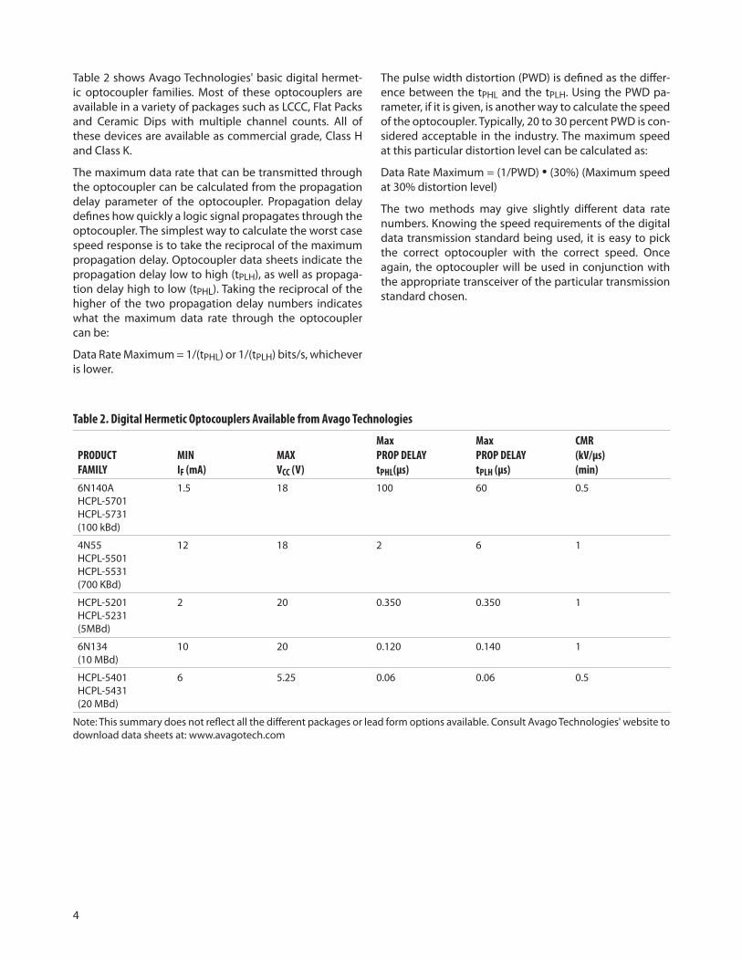
Table 2 shows Avago Technologies' basic digital hermet-ic optocoupler families. Most of these optocouplers are available in a variety of packages such as LCCC, Flat Packs and Ceramic Dips with multiple channel counts. All of these devices are available as commercial grade, Class H and Class K.
The maximum data rate that can be transmitted through the optocoupler can be calculated from the propagation delay parameter of the optocoupler. Propagation delay defines how quickly a logic signal propagates through the optocoupler. The simplest way to calculate the worst case speed response is to take the reciprocal of the maximum propagation delay. Optocoupler data sheets indicate the propagation delay low to high (tPLH), as well as propaga-tion delay high to low (tPHL). Taking the reciprocal of the higher of the two propagation delay numbers indicates what the maximum data rate through the optocoupler can be:
Data Rate Maximum = 1/(tPHL) or 1/(tPLH) bits/s, whichever is lower.
The pulse width distortion (PWD) is defined as the differ-ence between the tPHL and the tPLH. Using the PWD pa-rameter, if it is given, is another way to calculate the speed of the optocoupler. Typically, 20 to 30 percent PWD is con-sidered acceptable in the industry. The maximum speed at this particular distortion level can be calculated as:
Data Rate Maximum = (1/PWD) • (30%) (Maximum speed at 30% distortion level)
The two methods may give slightly different data rate numbers. Knowing the speed requirements of the digital data transmission standard being used, it is easy to pick the correct optocoupler with the correct speed. Once again, the optocoupler will be used in conjunction with the appropriate transceiver of the particular transmission standard chosen.
Table 2. Digital Hermetic Optocouplers Available from Avago Technologies
PRODUCTFAMILY
MINIF (mA)
MAXVCC (V)
MaxPROP DELAYtPHL(µs)
Max PROP DELAY tPLH (µs)
CMR(kV/µs)(min)
6N140AHCPL-5701 HCPL-5731 (100 kBd)
1.5 18 100 60 0.5
4N55 HCPL-5501 HCPL-5531 (700 KBd)
12 18 2 6 1
HCPL-5201 HCPL-5231 (5MBd)
2 20 0.350 0.350 1
6N134 (10 MBd)
10 20 0.120 0.140 1
HCPL-5401 HCPL-5431 (20 MBd)
6 5.25 0.06 0.06 0.5
Note: This summary does not reflect all the different packages or lead form options available. Consult Avago Technologies' website to download data sheets at: www.avagotech.com
5
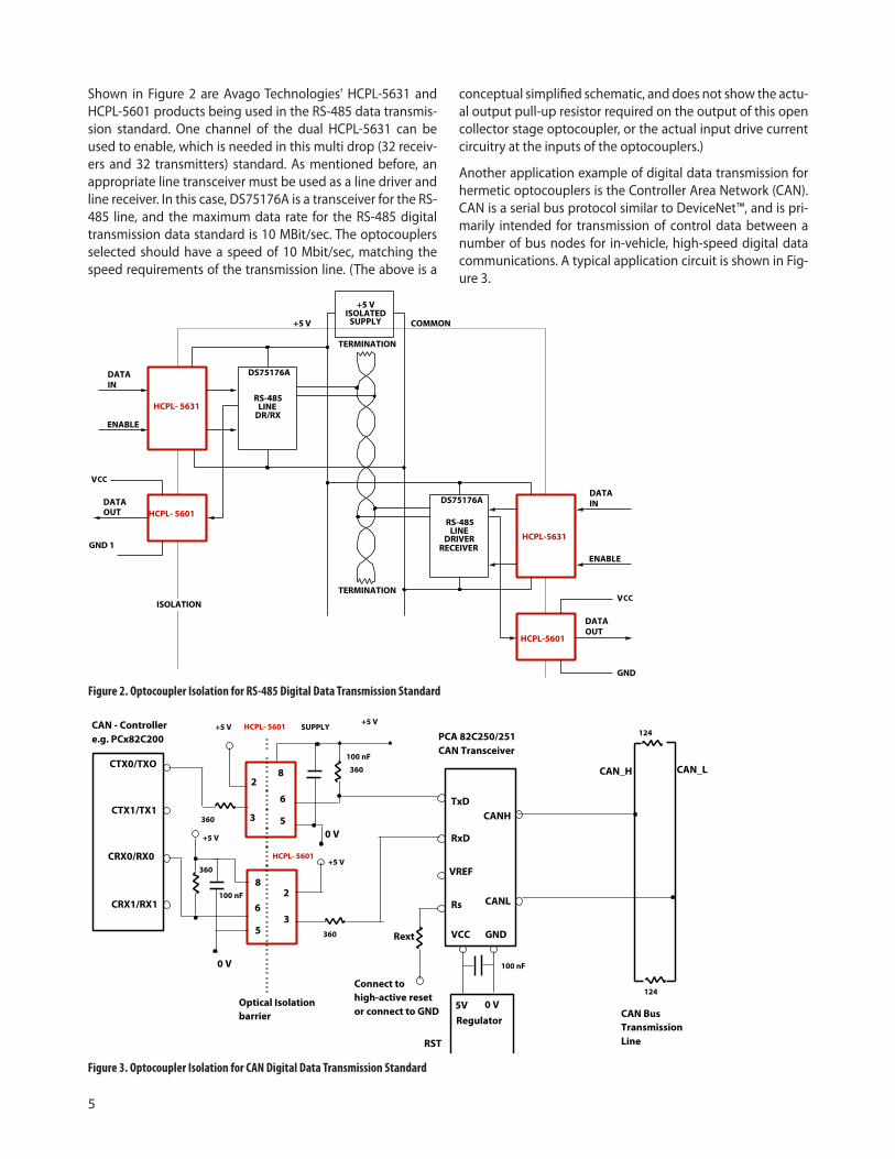
Shown in Figure 2 are Avago Technologies' HCPL-5631 and HCPL-5601 products being used in the RS-485 data transmis-sion standard. One channel of the dual HCPL-5631 can be used to enable, which is needed in this multi drop (32 receiv-ers and 32 transmitters) standard. As mentioned before, an appropriate line transceiver must be used as a line driver and line receiver. In this case, DS75176A is a transceiver for the RS-485 line, and the maximum data rate for the RS-485 digital transmission data standard is 10 MBit/sec. The optocouplers selected should have a speed of 10 Mbit/sec, matching the speed requirements of the transmission line. (The above is a
conceptual simplified schematic, and does not show the actu-al output pull-up resistor required on the output of this open collector stage optocoupler, or the actual input drive current circuitry at the inputs of the optocouplers.)
Another application example of digital data transmission for hermetic optocouplers is the Controller Area Network (CAN). CAN is a serial bus protocol similar to DeviceNet™, and is pri-marily intended for transmission of control data between a number of bus nodes for in-vehicle, high-speed digital data communications. A typical application circuit is shown in Fig-ure 3.
Figure 3. Optocoupler Isolation for CAN Digital Data Transmission Standard
Figure 2. Optocoupler Isolation for RS-485 Digital Data Transmission Standard
+5 V SUPPLY+5 V
HCPL- 5601CAN - Controllere.g. PCx82C200
CTX0/TXO
CTX1/TX1
CRX0/RX0
CRX1/RX1
CAN_H CAN_L
HCPL- 5601
3
2
5
8
6
360
360
0 V
2
3
8
6
5
+5 V
0 V
360
360
124
124
100 nF
+5 V
100 nF
PCA 82C250/251CAN Transceiver
CANH
CANL
TxD
RxD
VREF
Rs
GNDVCC
5VRegulator
RST
Rext
0 V
Connect tohigh-active resetor connect to GND
100 nF
Optical Isolationbarrier CAN Bus
TransmissionLine
RS-485 LINE
DR/RX
RS-485 LINE
DRIVER RECEIVER
HCPL- 5631
HCPL-5631
TERMINATION
DATA IN
ENABLE
DATA OUT
DATA IN
ENABLE
VCC
DATA OUT
GND
VCC
GND 1
ISOLATION
TERMINATION
DS75176A
DS75176A
+5 V ISOLATED
SUPPLY+5 V COMMON
HCPL- 5601
HCPL-5601
6
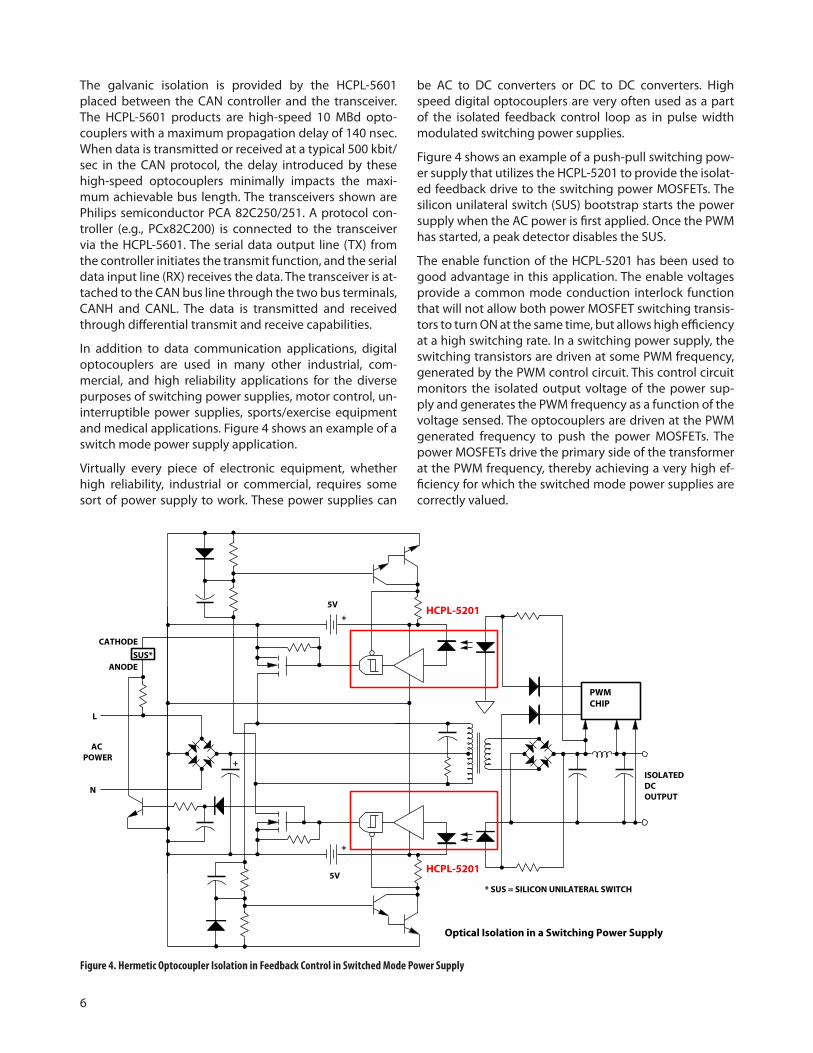
The galvanic isolation is provided by the HCPL-5601 placed between the CAN controller and the transceiver. The HCPL-5601 products are high-speed 10 MBd opto-couplers with a maximum propagation delay of 140 nsec. When data is transmitted or received at a typical 500 kbit/sec in the CAN protocol, the delay introduced by these high-speed optocouplers minimally impacts the maxi-mum achievable bus length. The transceivers shown are Philips semiconductor PCA 82C250/251. A protocol con-troller (e.g., PCx82C200) is connected to the transceiver via the HCPL-5601. The serial data output line (TX) from the controller initiates the transmit function, and the serial data input line (RX) receives the data. The transceiver is at-tached to the CAN bus line through the two bus terminals, CANH and CANL. The data is transmitted and received through differential transmit and receive capabilities.
In addition to data communication applications, digital optocouplers are used in many other industrial, com-mercial, and high reliability applications for the diverse purposes of switching power supplies, motor control, un-interruptible power supplies, sports/exercise equipment and medical applications. Figure 4 shows an example of a switch mode power supply application.
Virtually every piece of electronic equipment, whether high reliability, industrial or commercial, requires some sort of power supply to work. These power supplies can
Figure 4. Hermetic Optocoupler Isolation in Feedback Control in Switched Mode Power Supply
be AC to DC converters or DC to DC converters. High speed digital optocouplers are very often used as a part of the isolated feedback control loop as in pulse width modulated switching power supplies.
Figure 4 shows an example of a push-pull switching pow-er supply that utilizes the HCPL-5201 to provide the isolat-ed feedback drive to the switching power MOSFETs. The silicon unilateral switch (SUS) bootstrap starts the power supply when the AC power is first applied. Once the PWM has started, a peak detector disables the SUS.
The enable function of the HCPL-5201 has been used to good advantage in this application. The enable voltages provide a common mode conduction interlock function that will not allow both power MOSFET switching transis-tors to turn ON at the same time, but allows high efficiency at a high switching rate. In a switching power supply, the switching transistors are driven at some PWM frequency, generated by the PWM control circuit. This control circuit monitors the isolated output voltage of the power sup-ply and generates the PWM frequency as a function of the voltage sensed. The optocouplers are driven at the PWM generated frequency to push the power MOSFETs. The power MOSFETs drive the primary side of the transformer at the PWM frequency, thereby achieving a very high ef-ficiency for which the switched mode power supplies are correctly valued.
AC POWER
PWM CHIP
L
N
5V +
HCPL-5201
5V
+
HCPL-5201
+ISOLATED DC OUTPUT
Optical Isolation in a Switching Power Supply
SUS*CATHODE
ANODE
* SUS = SILICON UNILATERAL SWITCH
7
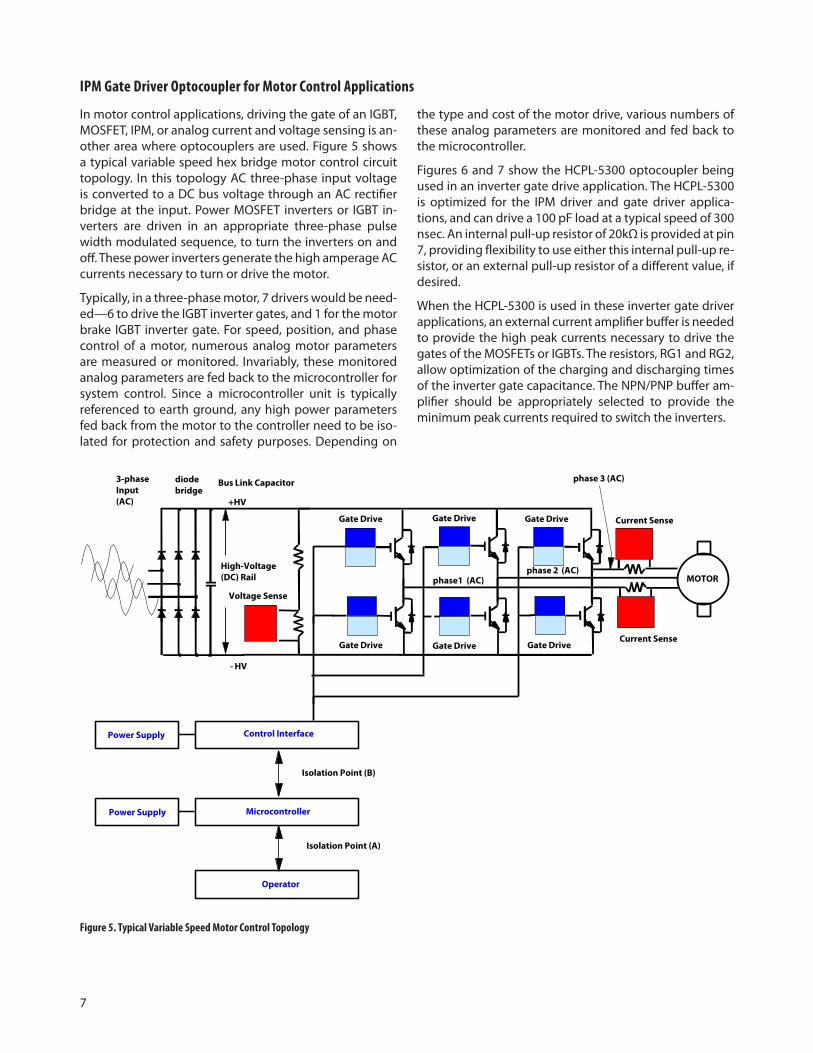
Figure 5. Typical Variable Speed Motor Control Topology
the type and cost of the motor drive, various numbers of these analog parameters are monitored and fed back to the microcontroller.
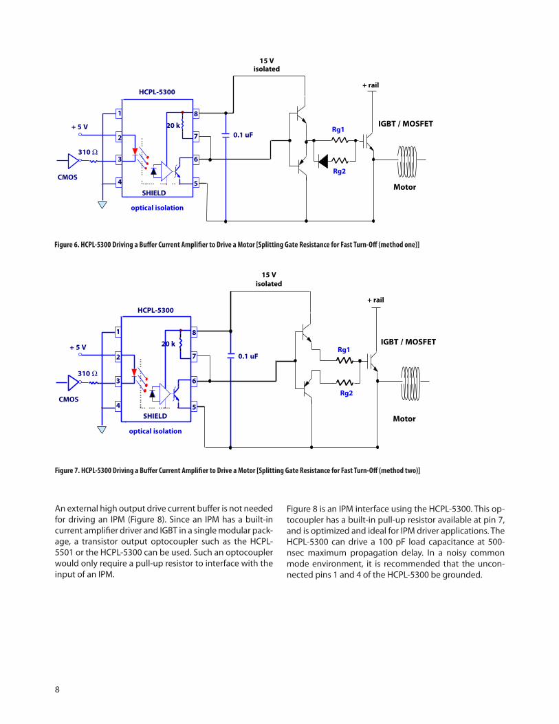
Figures 6 and 7 show the HCPL-5300 optocoupler being used in an inverter gate drive application. The HCPL-5300 is optimized for the IPM driver and gate driver applica-tions, and can drive a 100 pF load at a typical speed of 300 nsec. An internal pull-up resistor of 20kΩ is provided at pin 7, providing flexibility to use either this internal pull-up re-sistor, or an external pull-up resistor of a different value, if desired.
When the HCPL-5300 is used in these inverter gate driver applications, an external current amplifier buffer is needed to provide the high peak currents necessary to drive the gates of the MOSFETs or IGBTs. The resistors, RG1 and RG2, allow optimization of the charging and discharging times of the inverter gate capacitance. The NPN/PNP buffer am-plifier should be appropriately selected to provide the minimum peak currents required to switch the inverters.
In motor control applications, driving the gate of an IGBT, MOSFET, IPM, or analog current and voltage sensing is an-other area where optocouplers are used. Figure 5 shows a typical variable speed hex bridge motor control circuit topology. In this topology AC three-phase input voltage is converted to a DC bus voltage through an AC rectifier bridge at the input. Power MOSFET inverters or IGBT in-verters are driven in an appropriate three-phase pulse width modulated sequence, to turn the inverters on and off. These power inverters generate the high amperage AC currents necessary to turn or drive the motor.
Typically, in a three-phase motor, 7 drivers would be need-ed—6 to drive the IGBT inverter gates, and 1 for the motor brake IGBT inverter gate. For speed, position, and phase control of a motor, numerous analog motor parameters are measured or monitored. Invariably, these monitored analog parameters are fed back to the microcontroller for system control. Since a microcontroller unit is typically referenced to earth ground, any high power parameters fed back from the motor to the controller need to be iso-lated for protection and safety purposes. Depending on
MOTOR
Gate Drive Gate Drive Gate DriveCurrent Sense
Voltage Sense
Control Interface
- HV
+HV
High-Voltage(DC) Rail
3-phaseInput(AC)
diodebridge
phase1 (AC)phase 2 (AC)
phase 3 (AC)
Microcontroller
Operator
Power Supply
Gate Drive Gate Drive Gate Drive Current Sense
Bus Link Capacitor
Isolation Point (A)
Isolation Point (B)
Power Supply
IPM Gate Driver Optocoupler for Motor Control Applications
8
Figure 6. HCPL-5300 Driving a Buffer Current Amplifier to Drive a Motor [Splitting Gate Resistance for Fast Turn-Off (method one)]
15 Visolated
+ rail
IGBT / MOSFET
Motor
1
2
3
4 5
6
7
8
SHIELD
20 k
HCPL-5300
+ 5 V
310 Ω
CMOS
optical isolation
Rg1
Rg2
0.1 uF
15 Visolated
+ rail
IGBT / MOSFET
Motor
1
2
3
4 5
6
7
8
SHIELD
20 k
HCPL-5300
0.1 uF + 5 V
310 Ω
CMOS
optical isolation
Rg1
Rg2
Figure 7. HCPL-5300 Driving a Buffer Current Amplifier to Drive a Motor [Splitting Gate Resistance for Fast Turn-Off (method two)]
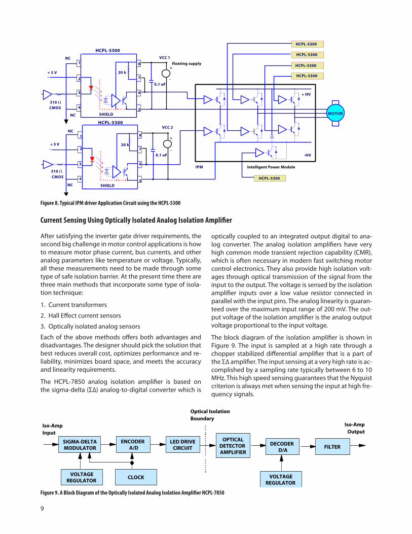
An external high output drive current buffer is not needed for driving an IPM (Figure 8). Since an IPM has a built-in current amplifier driver and IGBT in a single modular pack-age, a transistor output optocoupler such as the HCPL-5501 or the HCPL-5300 can be used. Such an optocoupler would only require a pull-up resistor to interface with the input of an IPM.
Figure 8 is an IPM interface using the HCPL-5300. This op-tocoupler has a built-in pull-up resistor available at pin 7, and is optimized and ideal for IPM driver applications. The HCPL-5300 can drive a 100 pF load capacitance at 500-nsec maximum propagation delay. In a noisy common mode environment, it is recommended that the uncon-nected pins 1 and 4 of the HCPL-5300 be grounded.
9
Figure 8. Typical IPM driver Application Circuit using the HCPL-5300
optically coupled to an integrated output digital to ana-log converter. The analog isolation amplifiers have very high common mode transient rejection capability (CMR), which is often necessary in modern fast switching motor control electronics. They also provide high isolation volt-ages through optical transmission of the signal from the input to the output. The voltage is sensed by the isolation amplifier inputs over a low value resistor connected in parallel with the input pins. The analog linearity is guaran-teed over the maximum input range of 200 mV. The out-put voltage of the isolation amplifier is the analog output voltage proportional to the input voltage.
The block diagram of the isolation amplifier is shown in Figure 9. The input is sampled at a high rate through a chopper stabilized differential amplifier that is a part of the Σ∆ amplifier. The input sensing at a very high rate is ac-complished by a sampling rate typically between 6 to 10 MHz. This high speed sensing guarantees that the Nyquist criterion is always met when sensing the input at high fre-quency signals.
After satisfying the inverter gate driver requirements, the second big challenge in motor control applications is how to measure motor phase current, bus currents, and other analog parameters like temperature or voltage. Typically, all these measurements need to be made through some type of safe isolation barrier. At the present time there are three main methods that incorporate some type of isola-tion technique:
1. Current transformers
2. Hall Effect current sensors
3. Optically isolated analog sensors
Each of the above methods offers both advantages and disadvantages. The designer should pick the solution that best reduces overall cost, optimizes performance and re-liability, minimizes board space, and meets the accuracy and linearity requirements.
The HCPL-7850 analog isolation amplifier is based on the sigma-delta (Σ∆) analog-to-digital converter which is
Figure 9. A Block Diagram of the Optically Isolated Analog Isolation Amplifier HCPL-7850
SIGMA-DELTAMODULATOR
ENCODERA/D
LED DRIVECIRCUIT
OPTICALDETECTORAMPLIFIER
DECODERD/A FILTER
Optical IsolationBoundary
Iso-AmpInput
Iso-AmpOutput
VOLTAGEREGULATOR
VOLTAGEREGULATOR CLOCK
-HV
+ HV
1
2
3
4 5
6
7
8
SHIELD
20 k
HCPL-5300
1
2
3
4 5
6
7
8
SHIELD
20 k
HCPL-5300
IPM
MOTOR
HCPL-5300
HCPL-5300
HCPL-5300
HCPL-5300
HCPL-5300
+ 5 V
+ 5 V
310 Ω
310 Ω
CMOS
CMOS
floating supply
Intelligent Power Module
0.1 uF
VCC 1
0.1 uF
VCC 2
+
-
+
-
NC
NC
NC
NC
Current Sensing Using Optically Isolated Analog Isolation Amplifier

10
Figure 10. Typical Current Sensing Application Circuit using the HCPL-7850 Amplifier
HV+
1
2
3
4
HCPL-7850
0.01 µF
0.1 µF
+ SUPPLY
+MOTOR
78L05
IN OUT
0.1 µF
HV-
R SENSE
8
7
6
5
+5 V+15 V
0.1 µF
0.1 µF
0.1 µF
10.0 kΩ150 pF
2.00 kΩ
2.00 kΩ
-15 V
MC34082A+
-V
150 pF
6
5
8
4
7
10.0 kΩ
39 Ω
+5 V
ISOLATIONBOUNDARY
-
Figure 11. Typical Voltage Sensing Application Circuit using the HCPL-7850 Amplifier
HV+
1
2
3
4
HCPL-7850
0.01 µF
0.1 µF
+ SUPPLY
+
78L05
IN OUT
0.1 µF
HV-
R1SENSE
8
7
6
5
+5 V+15 V
0.1 µF
0.1 µF
0.1 µF
10.0 kΩ150 pF
2.00 kΩ
2.00 kΩ
-15 V
MC34082A+
-V
150 pF
6
5
8
4
7
10.0 kΩ
39 Ω
+5 V
ISOLATION BOUNDARY
-
R2
In operation, the Σ∆ modulator converts the analog input signal into high-speed serial bit streams. The time aver-age of this bit stream is directly proportional to the input signal. This stream of digital data is encoded and optically transferred to the detector circuit. The detected signal is decoded and converted back into the analog signal, which is filtered to obtain the final output signal. Figure 10 shows a typical application circuit for motor phase cur-rent measurements.
The input is sensed across a precision, low resistance, low inductance, and low temperature co-efficient shunt resis-tor. A low pass RC filter at the input (39 Ω resistor and 0.01 µF capacitor) rejects high frequency noise components and is an anti-aliasing filter. The post differential amplifier converts the differential output signal of the isolation am-plifier to a ground referenced voltage compatible with an A/D converter at the microcontroller. The differential am-plifier’s bandwidth can be adjusted by the RC filter on the feedback path to reject and to minimize the noise at the output, if necessary.
Use the HCPL-7850 for DC bus current or AC phase cur-rent sensing, voltage sensing for bus voltage, temperature sensing (voltage from temperature sensor of the heat sink of the IGBT or IPM), or counter electromotive voltage sens-ing of the motor (for brushless DC motors only). Figure 10 shows the HCPL-7850 in a motor phase current sensing to-pology. In Figure 11 a suitable voltage divider at the input (such that the sensing voltage is below 200-mV absolute value) is used to measure the bus voltage or counter emf of brushless DC motors.
In this case, the constraint is that the value of R1 should be kept below 1kΩ, such that input impedance of the HCPL-7850 (280 kΩ) and input current (1 µA typical) do not in-troduce offsets and inaccuracies in the measurement. An input bypass capacitor of 0.01 µF is still required, although the 39 Ω resistor can be omitted, as the voltage divider resistor will perform the same low pass filter function.
11
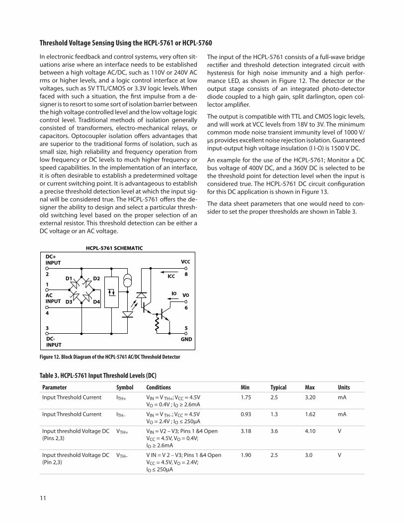
Figure 12. Block Diagram of the HCPL-5761 AC/DC Threshold Detector
In electronic feedback and control systems, very often sit-uations arise where an interface needs to be established between a high voltage AC/DC, such as 110V or 240V AC rms or higher levels, and a logic control interface at low voltages, such as 5V TTL/CMOS or 3.3V logic levels. When faced with such a situation, the first impulse from a de-signer is to resort to some sort of isolation barrier between the high voltage controlled level and the low voltage logic control level. Traditional methods of isolation generally consisted of transformers, electro-mechanical relays, or capacitors. Optocoupler isolation offers advantages that are superior to the traditional forms of isolation, such as small size, high reliability and frequency operation from low frequency or DC levels to much higher frequency or speed capabilities. In the implementation of an interface, it is often desirable to establish a predetermined voltage or current switching point. It is advantageous to establish a precise threshold detection level at which the input sig-nal will be considered true. The HCPL-5761 offers the de-signer the ability to design and select a particular thresh-old switching level based on the proper selection of an external resistor. This threshold detection can be either a DC voltage or an AC voltage.
5
ICC
GND
6
VO
8
VCC
3
2
1
4
DC+ INPUT
AC INPUT
DC- INPUT
IO
HCPL-5761 SCHEMATIC
D1 D2
D3 D4
Table 3. HCPL-5761 Input Threshold Levels (DC)
Parameter Symbol Conditions Min Typical Max UnitsInput Threshold Current ITH+ VIN = V TH+; VCC = 4.5V
VO = 0.4V ; IO ≥ 2.6mA1.75 2.5 3.20 mA
Input Threshold Current ITH– VIN = V TH–; VCC = 4.5VVO = 2.4V ; IO ≤ 250µA
0.93 1.3 1.62 mA
Input threshold Voltage DC (Pins 2,3)
VTH+ VIN = V2 – V3; Pins 1 &4 OpenVCC = 4.5V, VO = 0.4V;IO ≥ 2.6mA
3.18 3.6 4.10 V
Input threshold Voltage DC (Pin 2,3)
VTH– V IN = V 2 – V3; Pins 1 &4 OpenVCC = 4.5V, VO = 2.4V;IO ≤ 250µA
1.90 2.5 3.0 V
The input of the HCPL-5761 consists of a full-wave bridge rectifier and threshold detection integrated circuit with hysteresis for high noise immunity and a high perfor-mance LED, as shown in Figure 12. The detector or the output stage consists of an integrated photo-detector diode coupled to a high gain, split darlington, open col-lector amplifier.
The output is compatible with TTL and CMOS logic levels, and will work at VCC levels from 18V to 3V. The minimum common mode noise transient immunity level of 1000 V/µs provides excellent noise rejection isolation. Guaranteed input-output high voltage insulation (I I-O) is 1500 V DC.
An example for the use of the HCPL-5761; Monitor a DC bus voltage of 400V DC, and a 360V DC is selected to be the threshold point for detection level when the input is considered true. The HCPL-5761 DC circuit configuration for this DC application is shown in Figure 13.
The data sheet parameters that one would need to con-sider to set the proper thresholds are shown in Table 3.
Threshold Voltage Sensing Using the HCPL-5761 or HCPL-5760
12
UP TO 1500 V DC
VOUT
HCPL-5761
R LRX/2
V CC
1
2
3
4
8
7
6
5
DC INPUT CONFIGURATION
RX/2
+ Rail Voltage
- Rail Voltage
400V
To microcontroller
GND 1
GND 2Optical Isolation
Barrier
1.8 kΩ
Now, determine the power rating of the external resistor (RX). The calculation of the maximum power dissipation in RX is determined by knowing which of the following in-equalities is true, where VIHC3 is the input clamp voltage for this dc-input case:
(V+) / (Vpeak) > (VTH+) / (VIHC3) (VIN will not clamp)
(V≠) / (Vpeak) < (VTH+) / (VIHC3) (VIN will clamp)
Since, 360/400 > 3.6/12, the input will not clamp.
The DC input of the HCPL-5761 appears as a 1000Ω in series with a one volt offset. And, if the AC pins (1,4) are left unconnected as in this example, the DC input voltage can increase to 12V (two Zener diode voltages) before the onset of input voltage clamping occurs (VIHC3). Con-sequently, a conservative value for the maximum power dissipation in RX for the unclamped input (ignoring the input offset voltage) can be calculated as:
PRX = [Vpeak (RX /(RRX + 1kΩ)]2 / RX
=[400 (142.56kΩ / (142.56kΩ + 1kΩ)]2 / 142.56kΩ
= 1.1 W
A 1.25 W resistor is recommended to provide a margin of safety. If the inequality for clamped condition is true, the following equation can be used to easily calculate the power dissipated under that condition.
PRX = [ Vpeak – VIHC] 2 / RX
= [400 – 12] 2 /142.56kΩ
= 1.056 W (again choose 1.25 W resistor for a safe-ty margin)
The maximum input current and power must be calcu-lated to ensure the operating conditions are within the absolute maximum ratings of the HCPL-5760.
Let’s assume that we are planning to use the HCPL-5761 in a DC bus voltage threshold detection application in a mo-tor control application. The HCPL-5761 will sense the DC high voltage bus of 400V DC, and provide a digital signal to the microcontroller that is controlling the motor.
DC bus voltage to be monitored = 400V DC (Vpeak)
Switching threshold selected V+ = 360 V DC
Typical HCPL-5761 Input Levels:
V TH+ = 3.6 V
V TH– = 2.5 V
I TH+ = 2.5 mA
I TH– = 1.3 mA
(Input Clamp Voltage) VIHC3 = 12V
Now, calculate the value of the external resistor RX neces-sary to establish the required threshold detection level of 36 V DC. The threshold equation is:
RX = (V+ – V TH+) / (I TH+)
= (360 –3.6) / (2.5 mA)
= 142.56 kΩ
It is recommended that to improve common mode noise immunity and to provide equal impedance on the two sides of the input pins (2,3), this impedance of 142.56 kΩ be split in two equal halves, and one half resistor RX/2 of 71.28 kΩ be used at each of the two input pins.
The resultant lower threshold level (V–), because of the hysteresis provided at the input circuit of the HCPL-5761, is calculated as:
V – = (ITH+ • RX) + V TH+
= 1.3 mA • 142.56 kΩ + 2.5V
= 187.8 V
Figure 13. DC Bus Voltage Detection using the HCPL-5761
13
Figure 14. AC Power Line Detection Using the HCPL-5761
For the input clamped condition,
IIN = (Vpeak – VIHC) / RX < IIN (max)
= (400 – 12) / 142.56 kΩ
= 2.3 mA < 15 mA (max)
PIN = (VIHC • IIN ) < PIN (max
= 12 V • 2.3mA = 27 mW < 195 mW (max)
Since the output stage of the HCPL-5761 is an open col-lector stage, a pull-up resistor is required to make the op-tocoupler switch. An output pull-up resistor of 1.8kΩ is consistent with the gain and current transfer ratio of the optocoupler when the output VCC is 5V.
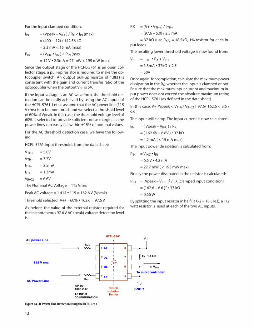
If the input voltage is an AC waveform, the threshold de-tection can be easily achieved by using the AC inputs of the HCPL-5761. Let us assume that the AC power line (115 V rms) is to be monitored, and we select a threshold level of 60% of Vpeak. In this case, the threshold voltage level of 60% is selected to provide sufficient noise margin, as the power lines can easily fall within ±15% of nominal values.
For the AC threshold detection case, we have the follow-ing:
HCPL-5761 Input thresholds from the data sheet:
VTH+ = 5.0V
VTH– = 3.7V
ITH+ = 2.5mA
ITH– = 1.3mA
VIHC2 = 6.6V
The Nominal AC Voltage = 115 Vrms
Peak AC voltage = 1.414 • 115 = 162.6 V (Vpeak)
Threshold selected (V+) = 60% • 162.6 = 97.6 V
As before, the value of the external resistor required for the instantaneous 97.6 V AC (peak) voltage detection level is:
RX = (V+ • VTH+) / I TH+
= (97.6 – 5.0) / 2.5 mA
= 37 kΩ (use RX/2 = 18.5kΩ, 1% resistor for each in-put lead)
The resulting lower threshold voltage is now found from:
V– = I TH– • RX + VTH–
= 1.3mA • 37kΩ + 2.5
= 50V
Once again, for completion, calculate the maximum power dissipation in the RX, whether the input is clamped or not. Ensure that the maximum input current and maximum in-put power does not exceed the absolute maximum rating of the HCPL-5761 (as defined in the data sheet).
In this case, V+ /Vpeak < VTH+/ VIHC2 [ 97.6/ 162.6 < 3.6 / 6.6 ]
The input will clamp. The input current is now calculated:
IIN = ( Vpeak – VIHC ) / RX
= ( 162.6V – 6.6V ) / 37 kΩ
= 4.2 mA ( < 15 mA max)
The input power dissipation is calculated from:
PIN = VIHC • IIN = 6.6 V • 4.2 mA
= 27.7 mW ( < 195 mW max)
Finally the power dissipated in the resistor is calculated:
PRX = [Vpeak – VIHC ]2 / RX (clamped input condition)
= [162.6 – 6.6 ]2 / 37 kΩ
= 0.66 W
By splitting the input resistor in half (R X/2 = 18.5 kΩ), a 1/2 watt resistor is used at each of the two AC inputs.
UP TO 1000 V AC
VOUT
HCPL-5761
R L
RX/2
VCC
1
2
3
4
8
7
6
5
AC INPUT CONFIGURATION
RX/2
AC power Line
AC Power Line
To microcontroller
GND 2Optical Isolation
Barrier
1.8 kΩ
115 V rms
AC
AC
DC
DC
14
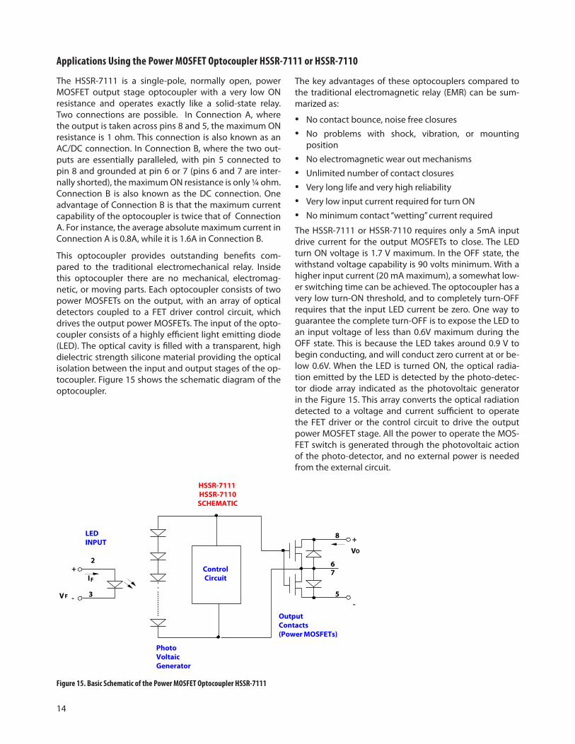
Figure 15. Basic Schematic of the Power MOSFET Optocoupler HSSR-7111
The HSSR-7111 is a single-pole, normally open, power MOSFET output stage optocoupler with a very low ON resistance and operates exactly like a solid-state relay. Two connections are possible. In Connection A, where the output is taken across pins 8 and 5, the maximum ON resistance is 1 ohm. This connection is also known as an AC/DC connection. In Connection B, where the two out-puts are essentially paralleled, with pin 5 connected to pin 8 and grounded at pin 6 or 7 (pins 6 and 7 are inter-nally shorted), the maximum ON resistance is only ¼ ohm. Connection B is also known as the DC connection. One advantage of Connection B is that the maximum current capability of the optocoupler is twice that of Connection A. For instance, the average absolute maximum current in Connection A is 0.8A, while it is 1.6A in Connection B.
This optocoupler provides outstanding benefits com-pared to the traditional electromechanical relay. Inside this optocoupler there are no mechanical, electromag-netic, or moving parts. Each optocoupler consists of two power MOSFETs on the output, with an array of optical detectors coupled to a FET driver control circuit, which drives the output power MOSFETs. The input of the opto-coupler consists of a highly efficient light emitting diode (LED). The optical cavity is filled with a transparent, high dielectric strength silicone material providing the optical isolation between the input and output stages of the op-tocoupler. Figure 15 shows the schematic diagram of the optocoupler.
HSSR-7111 HSSR-7110SCHEMATIC
2
V F
IF
3
+
-
8
5
VO
67
+
-
ControlCircuit
OutputContacts(Power MOSFETs)
PhotoVoltaicGenerator
LEDINPUT
Applications Using the Power MOSFET Optocoupler HSSR-7111 or HSSR-7110
The key advantages of these optocouplers compared to the traditional electromagnetic relay (EMR) can be sum-marized as:
• No contact bounce, noise free closures• No problems with shock, vibration, or mounting
position• No electromagnetic wear out mechanisms• Unlimited number of contact closures• Very long life and very high reliability• Very low input current required for turn ON• No minimum contact “wetting” current required
The HSSR-7111 or HSSR-7110 requires only a 5mA input drive current for the output MOSFETs to close. The LED turn ON voltage is 1.7 V maximum. In the OFF state, the withstand voltage capability is 90 volts minimum. With a higher input current (20 mA maximum), a somewhat low-er switching time can be achieved. The optocoupler has a very low turn-ON threshold, and to completely turn-OFF requires that the input LED current be zero. One way to guarantee the complete turn-OFF is to expose the LED to an input voltage of less than 0.6V maximum during the OFF state. This is because the LED takes around 0.9 V to begin conducting, and will conduct zero current at or be-low 0.6V. When the LED is turned ON, the optical radia-tion emitted by the LED is detected by the photo-detec-tor diode array indicated as the photovoltaic generator in the Figure 15. This array converts the optical radiation detected to a voltage and current sufficient to operate the FET driver or the control circuit to drive the output power MOSFET stage. All the power to operate the MOS-FET switch is generated through the photovoltaic action of the photo-detector, and no external power is needed from the external circuit.
15
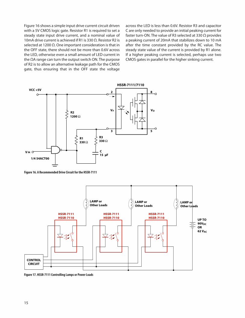
Figure 16 shows a simple input drive current circuit driven with a 5V CMOS logic gate. Resistor R1 is required to set a steady state input drive current, and a nominal value of 10mA drive current is achieved if R1 is 330 Ω. Resistor R2 is selected at 1200 Ω. One important consideration is that in the OFF state, there should not be more than 0.6V across the LED, otherwise even a small amount of LED current in the ΩA range can turn the output switch ON. The purpose of R2 is to allow an alternative leakage path for the CMOS gate, thus ensuring that in the OFF state the voltage
Figure 16. A Recommended Drive Circuit for the HSSR-7111
across the LED is less than 0.6V. Resistor R3 and capacitor C are only needed to provide an initial peaking current for faster turn-ON. The value of R3 selected at 330 Ω provides a peaking current of 20mA that stabilizes down to 10 mA after the time constant provided by the RC value. The steady state value of the current is provided by R1 alone. If a higher peaking current is selected, perhaps use two CMOS gates in parallel for the higher sinking current.
Figure 17. HSSR-7111 Controlling Lamps or Power Loads
HSSR-7111HSSR-7110
CONTROLCIRCUIT
LAMP orOther Loads
HSSR-7111HSSR-7110
LAMP orOther Loads
HSSR-7111HSSR-7110
LAMP orOther Loads
UP TO 90VDCOR 62 VAC
V IN
R2
2
HSSR-7111/7110
VF
3
8
5
VO
1200 Ω
330 ΩR1
1/4 54ACT0015 µF
330 ΩR3
VCC +5V
C
16
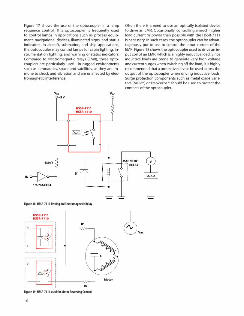
Figure 17 shows the use of the optocoupler in a lamp sequence control. This optocoupler is frequently used to control lamps in applications such as process equip-ment, navigational devices, illuminated signs, and status indicators. In aircraft, submarine, and ship applications, the optocoupler may control lamps for cabin lighting, in-strumentation lighting, and warning or status indicators. Compared to electromagnetic relays (EMR), these opto-couplers are particularly useful in rugged environments such as aeronautics, space and satellites, as they are im-mune to shock and vibration and are unaffected by elec-tromagnetic interference.
Figure 18. HSSR-7111 Driving an Electromagnetic Relay
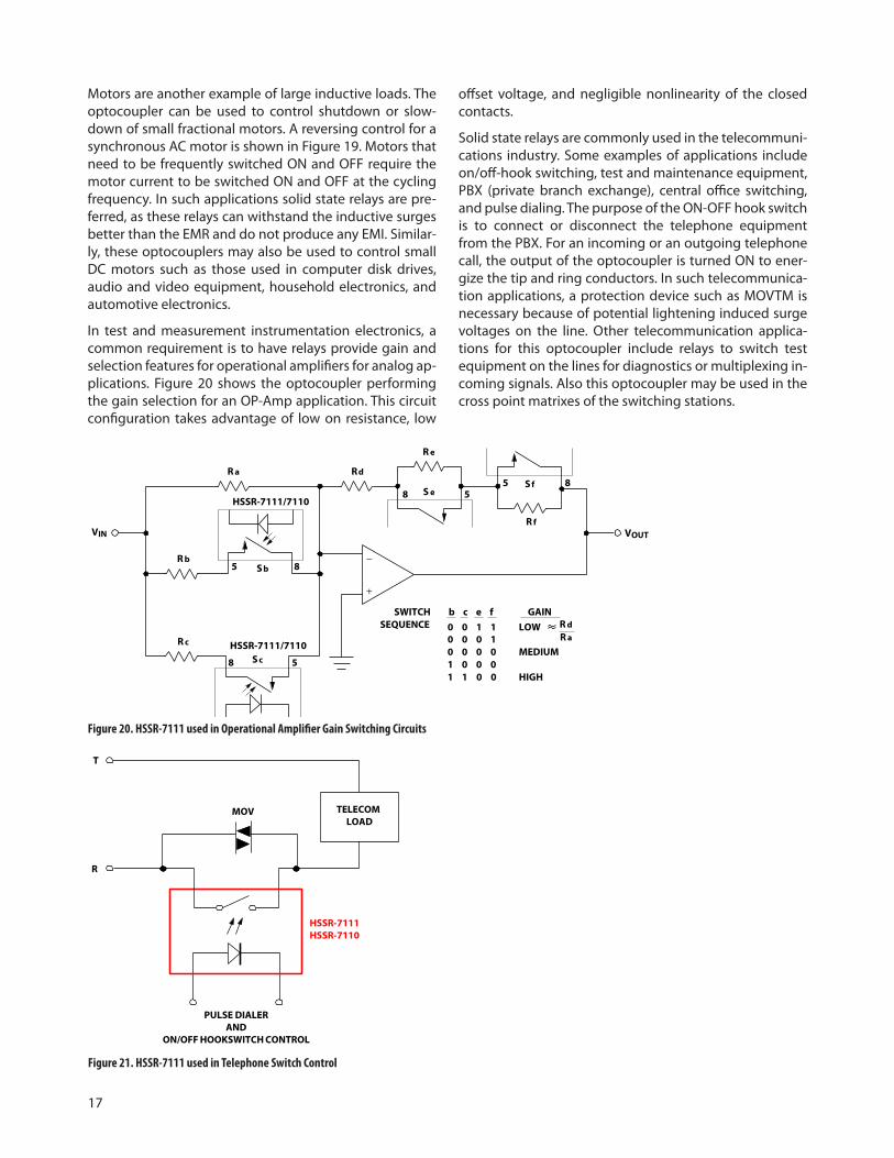
Often there is a need to use an optically isolated device to drive an EMR. Occasionally, controlling a much higher load current or power than possible with the HSSR-7111 is necessary. In such cases, the optocoupler can be advan-tageously put to use to control the input current of the EMR. Figure 18 shows the optocoupler used to drive an in-put coil of an EMR, which is a highly inductive load. Since inductive loads are prone to generate very high voltage and current surges when switching off the load, it is highly recommended that a protective device be used across the output of the optocoupler when driving inductive loads. Surge protection components such as metal oxide varis-tors (MOV™) or TranZorbs™ should be used to protect the contacts of the optocoupler.
Figure 19. HSSR-7111 used for Motor Reversing Control
Vac
C
HSSR-7111HSSR-7110
Motor
R1
R2
HSSR-7111HSSR-7110
LOAD
V
VDD
D1
MAGNETIC RELAY
VCC+5 V
IN
1/6 74ACT04
430 Ω
17
Motors are another example of large inductive loads. The optocoupler can be used to control shutdown or slow-down of small fractional motors. A reversing control for a synchronous AC motor is shown in Figure 19. Motors that need to be frequently switched ON and OFF require the motor current to be switched ON and OFF at the cycling frequency. In such applications solid state relays are pre-ferred, as these relays can withstand the inductive surges better than the EMR and do not produce any EMI. Similar-ly, these optocouplers may also be used to control small DC motors such as those used in computer disk drives, audio and video equipment, household electronics, and automotive electronics.
In test and measurement instrumentation electronics, a common requirement is to have relays provide gain and selection features for operational amplifiers for analog ap-plications. Figure 20 shows the optocoupler performing the gain selection for an OP-Amp application. This circuit configuration takes advantage of low on resistance, low
Figure 20. HSSR-7111 used in Operational Amplifier Gain Switching Circuits
offset voltage, and negligible nonlinearity of the closed contacts.
Solid state relays are commonly used in the telecommuni-cations industry. Some examples of applications include on/off-hook switching, test and maintenance equipment, PBX (private branch exchange), central office switching, and pulse dialing. The purpose of the ON-OFF hook switch is to connect or disconnect the telephone equipment from the PBX. For an incoming or an outgoing telephone call, the output of the optocoupler is turned ON to ener-gize the tip and ring conductors. In such telecommunica-tion applications, a protection device such as MOVTM is necessary because of potential lightening induced surge voltages on the line. Other telecommunication applica-tions for this optocoupler include relays to switch test equipment on the lines for diagnostics or multiplexing in-coming signals. Also this optocoupler may be used in the cross point matrixes of the switching stations.
Figure 21. HSSR-7111 used in Telephone Switch Control
T
R
PULSE DIALERAND
ON/OFF HOOKSWITCH CONTROL
HSSR-7111HSSR-7110
TELECOM LOAD
MOV
R c
VIN
SWITCH SEQUENCE
−
+
Rd
R e
S e8 5
R f
S f5 8
S c8 5
HSSR-7111/7110
S b5 8
HSSR-7111/7110
R b
R a
VOUT
b c e f GAIN0 0 1 1 0 0 0 1 0 0 0 0 1 0 0 0 1 1 0 0
LOW
MEDIUM
HIGH
R dR a
For product information and a complete list of distributors, please go to our web site: www.avagotech.com
Avago, Avago Technologies, and the A logo are trademarks of Avago Technologies in the United States and other countries.Data subject to change. Copyright © 2005-2010 Avago Technologies. All rights reserved. AV02-1895EN - March 17, 2010
ConclusionIn this article we have shown that Avago Technologies provides a wide portfolio of high reliability hermetic op-tocouplers that include modern, state of the art, reliable, sophisticated, and application specific optocouplers. Op-tocouplers are primarily used for noise rejection and high voltage safety and isolation purposes. Application specific hermetic optocouplers are available for diverse applica-tion needs. These applications include high speed digi-tal data communication applications, feedback sensing elements for switching power supplies, Intelligent Power Module (IPM) driver applications for motor control, analog optocouplers for current and voltage sensing applications, power MOSFET optocouplers for power load switching and telecommunication switching applications. Through extensive radiation tests performed to date, these her-metic optocouplers have been found to be radiation toler-ant to high levels. With proper design considerations, they may be used in applications encountering harsh environ-ments. The entire product offering is contained within Defense Supply Center Columbus (DSCC) Standard Mi-crocircuit Drawings (SMDs). Avago Technologies is listed as a QML-38534 supplier for both high reliability Class H devices and the highest reliability class K devices. All of these devices, including the full line of commercial level products, are considered COTS (Commercial Off the Shelf ) per the definition endorsed by the DSCC.
References[1] Paul R Gray and Robert G. Meyer, “Analysis and Design
of Analog Integrated Circuits,” Second Edition 1984, John Wiley and Sons, Inc.
[2] Paul Horowitz and Winfield Hill, “The Art of Electronics,” Second Edition 1989, Cambridge University Press
[3] Jamshed N. Khan, “Optocouplers For Variable Speed Motor Control Electronics in Consumer Home Appliances,” Conference Proceeding, 2000 Appliance Manufacturer Conference and Expo (AMCE), pp. 35-60, 2000
[4] Drew Plant and Mike Walters, “Isolation Amplifiers: Isolation for Sense Resistor Applications,” Principles of Current Sensors, Powersystems World, pp. 19-38, 1997
[5] Jamshed N. Khan, “Regulatory Guide to Isolation Circuits,” Hewlett-Packard Publication Number 5965-5853E, 1/1997
Radiation Tolerant Hermetic Optocouplers From Avago TechnologiesEven though the hermetic optocouplers manufactured by Avago Technologies may not be characterized as Rad- Hard, they have proven to be quite tolerant to most ra-diation effects. Avago Technologies' optocouplers utilize integrated photodiode detectors, whereas many opto-couplers use phototransistors in their designs. The pho-todiode design permits shallower diffusion depths and a smaller transistor base area. Phototransistor optocouplers, on the other hand, maximize the base area for increased coupling. This scheme makes the device very susceptible to radiation effects. At the same radiation level, the device with the smaller exposed sensitive area will experience less radiation damage.
Proton-induced single event transients (SET) have a high level of occurrence on high-speed optocouplers such as the Avago Technologies' 6N134/HCPL-56xx and HCPL-54xx product families. This is not surprising as photodi-odes make wonderful particle detectors. The high speed (bandwidth faster than 400 kbps) of some photodiodes allows some transients to induce a transient output. How-ever, there are workarounds (e.g., to increase the Vcc level or use the optocoupler in inverting mode rather than non-inverting mode, whichever appears to be less sensitive). For slower speed or bandwidth applications, less highly integrated or simpler optocouplers, such as the 4N55 product family or 6N140A family, are recommended. As this family exhibits a high rate of immunity to SET, it is an excellent example of the filtering capabilities of the slower speed optocoupler amplifier stage.
Total doses of up to 200Krads have been performed on the majority of the hermetic products. These have revealed a high degree of tolerance. With the exception of the “relay” devices (HSSR-711x), Avago Technologies has not experi-enced any device not meeting datasheet specifications af-ter 200Krads. The MOSFETs utilized in the HSSR-711x fam-ily have a low threshold voltage that requires thin oxide for the gates. This design allows for total dose radiation levels up to 30Krads before significant leakage occurs. Over the past several years, Avago Technologies has made a concerted effort to amass radiation data on our hermet-ic optocoupler portfolio. This data, consisting mostly of photons (gamma) and particles (protons and electrons), confirms our belief that the Avago Technologies' IC design provides high radiation immunity.