Embed Size (px)
Citation preview
Description
Avago Technologies’ ALM-1912 is a GPS front-end module that combines a GPS FBAR filter with high-gain low-noise amplifier (LNA).The LNA uses Avago Technologies’ pro-prietary GaAs Enhancement-mode pHEMT process to achieve high gain with very low noise figure and high linearity. Noise figure distribution is very tightly controlled. A CMOS-compatible shutdown pin is included either for turning the LNA on/off or for current adjustment. The filter use Avago Technologies’ leading-edge FBAR filter for low GPS band insertion loss and exceptional rejection at Cellular, PCS and WLAN band frequencies.
The low noise figure and high gain, coupled with low current consumption make it suitable for use in critical low-power GPS applications or during low-battery situations.
Component Image
Surface Mount 2.9 x 2.0 x 1 mm3 9-lead MCOB
Features
� Very Low Noise Figure
� Exceptional Cell/PCS/WLAN-Band rejection
� Low external component count
� Fully-matched at RF input and RF output
� Shutdown current : < 1 uA
� CMOS compatible shutdown pin (SD)
� ESD : > 3kV at RFin pin
� 2.9 x 2.0 x 0.95 mm size
� Adjustable bias current via single external resistor/voltage
� Lead-free and Halogen free
Specifications (Typical performance @ 25°C)
At 1.575GHz, Vdd = 2.7V, Idd = 6mA� Gain = 19.3 dB
� NF = 1.62 dB
� IIP3 = +1.5 dBm
� IP1dB = -8 dBm
� S11 = -9.5 dB
� S22 =-13.5 dB
� Cell-Band Rejection: > 57dBc
� PCS-Band Rejection: > 53dBc
� WLAN-Band Rejection: > 52dBc
Application
� GPS Front-end Module
Application Circuit
ALM-1912
GPS Filter–LNA Front–End Module
Data Sheet
Note: Package marking provides orientation and identification“1912” = Product Code “YY” = Year of manufacture“WW” = Work week of manufacture
RFin RFout
+Vdd = 2.7VVBias
LRBias
GPS
FilterLNA
Top View
RF In (pin 1)
Gnd (pin 2)
Gnd(pin 3)
Gnd(pin 4)
NC (pin5)
RF Out (pin 6)
Vdd (pin 7)
Gnd(pin 9)
Vsd(pin 8)
Bottom View
Gnd(pin 9)
Vsd(pin 8)
Vdd (pin 7)
Gnd (pin 2)
RF In (pin 1)
NC (pin 5)
RF Out (pin 6)
Gnd(pin 3)
Gnd(pin 4)
1912
WWYY
2
11 50 54 56 58 60
LSL USL
17 18 19 20 21 1.1 1.2 1.3 1.4 1.5 1.6 1.7 1.8 1.9 2.0 2.1
2 3 4 5 6 7 8 9 10
USL LSL
52
LSL LSL
44 46 48 50 52 54 56 42 44 46 48 50 52 54 56
Absolute Maximum Rating[1] TA=25°C
Symbol Parameter Units
Absolute
Max.
Vdd Device Frain to Source Voltage [2] V 4.5
Idd Drain Current [2] mA 15
Pin,max CW RF Input Power (Vdd = 2.7V. Idd = 6mA) dBm 13
Pdiss Total Power Dissipation[4] mW 54
TL Operating Temperature °C -40 to 85
Tj Junction Temperature °C 150
TSTG Storage Temperature °C -65 to 150
Thermal Resistance [3]
(Vdd = 2.7V, Idd = 6mA), �jc = 82.1°C/W
Notes:1. Operation of this device in excess of any of
these limits may cause permanent damage.2. Assuming DC quiescent conditions.3. Thermal resistance measured using Infra-Red
measurement technique.4. Board (module belly) temperature TB is 25°C.
Derate 4.2 mW/°C for TB>145.6°C.
Product Consistency Distribution Charts[5,6]
Figure 1. Gain at 1.575 GHz; LSL = 17dB, nominal = 19.3 dB Figure 2. NF at 1.575GHz; USL = 2dB, nominal = 1.62 dB
Figure 3. Id at 1.575 GHz; USL = 11.5 mA, nominal = 6mA
Notes:5. Distribution data sample size is 3000 samples taken from 3 different LNA wafers and 1 filter wafer. Future wafers allocated to this product may have
nominal values anywhere between the upper and lower limits.6. Measurements are made on a production test board, which represents a trade-off between optimal Gain, NF, IIP3, IP1dB, VSWR, Cell Band and PCS
Band Rejection. Circuit trace losses have not been de-embedded from actual measurements.
Figure 4. Cell band Rejection at 928MHz relative to 1.575 GHz; LSL = 51 dBc,
nominal = 57dBc
Figure 5. PCS band Rejection at 1710MHz relative to 1.575 GHz; LSL = 45dBc,
nominal = 52Bc
Figure 6. WLAN band Rejection at 2400MHz relative to 1.575 GHz; LSL =
43dBc, nominal = 51.5dBc
3
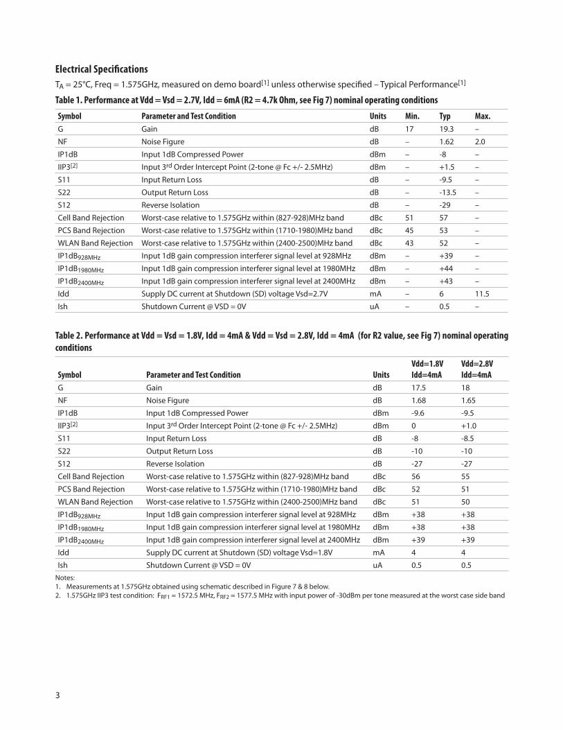
Electrical Specifications
TA = 25°C, Freq = 1.575GHz, measured on demo board[1] unless otherwise specified – Typical Performance[1]
Table 1. Performance at Vdd = Vsd = 2.7V, Idd = 6mA (R2 = 4.7k Ohm, see Fig 7) nominal operating conditions
Symbol Parameter and Test Condition Units Min. Typ Max.
G Gain dB 17 19.3 –
NF Noise Figure dB – 1.62 2.0
IP1dB Input 1dB Compressed Power dBm – -8 –
IIP3[2] Input 3rd Order Intercept Point (2-tone @ Fc +/- 2.5MHz) dBm – +1.5 –
S11 Input Return Loss dB – -9.5 –
S22 Output Return Loss dB – -13.5 –
S12 Reverse Isolation dB – -29 –
Cell Band Rejection Worst-case relative to 1.575GHz within (827-928)MHz band dBc 51 57 –
PCS Band Rejection Worst-case relative to 1.575GHz within (1710-1980)MHz band dBc 45 53 –
WLAN Band Rejection Worst-case relative to 1.575GHz within (2400-2500)MHz band dBc 43 52 –
IP1dB928MHz Input 1dB gain compression interferer signal level at 928MHz dBm – +39 –
IP1dB1980MHz Input 1dB gain compression interferer signal level at 1980MHz dBm – +44 –
IP1dB2400MHz Input 1dB gain compression interferer signal level at 2400MHz dBm – +43 –
Idd Supply DC current at Shutdown (SD) voltage Vsd=2.7V mA – 6 11.5
Ish Shutdown Current @ VSD = 0V uA – 0.5 –
Table 2. Performance at Vdd = Vsd = 1.8V, Idd = 4mA & Vdd = Vsd = 2.8V, Idd = 4mA (for R2 value, see Fig 7) nominal operating
conditions
Symbol Parameter and Test Condition Units
Vdd=1.8V
Idd=4mA
Vdd=2.8V
Idd=4mA
G Gain dB 17.5 18
NF Noise Figure dB 1.68 1.65
IP1dB Input 1dB Compressed Power dBm -9.6 -9.5
IIP3[2] Input 3rd Order Intercept Point (2-tone @ Fc +/- 2.5MHz) dBm 0 +1.0
S11 Input Return Loss dB -8 -8.5
S22 Output Return Loss dB -10 -10
S12 Reverse Isolation dB -27 -27
Cell Band Rejection Worst-case relative to 1.575GHz within (827-928)MHz band dBc 56 55
PCS Band Rejection Worst-case relative to 1.575GHz within (1710-1980)MHz band dBc 52 51
WLAN Band Rejection Worst-case relative to 1.575GHz within (2400-2500)MHz band dBc 51 50
IP1dB928MHz Input 1dB gain compression interferer signal level at 928MHz dBm +38 +38
IP1dB1980MHz Input 1dB gain compression interferer signal level at 1980MHz dBm +38 +38
IP1dB2400MHz Input 1dB gain compression interferer signal level at 2400MHz dBm +39 +39
Idd Supply DC current at Shutdown (SD) voltage Vsd=1.8V mA 4 4
Ish Shutdown Current @ VSD = 0V uA 0.5 0.5
Notes: 1. Measurements at 1.575GHz obtained using schematic described in Figure 7 & 8 below.2. 1.575GHz IIP3 test condition: FRF1 = 1572.5 MHz, FRF2 = 1577.5 MHz with input power of -30dBm per tone measured at the worst case side band
4
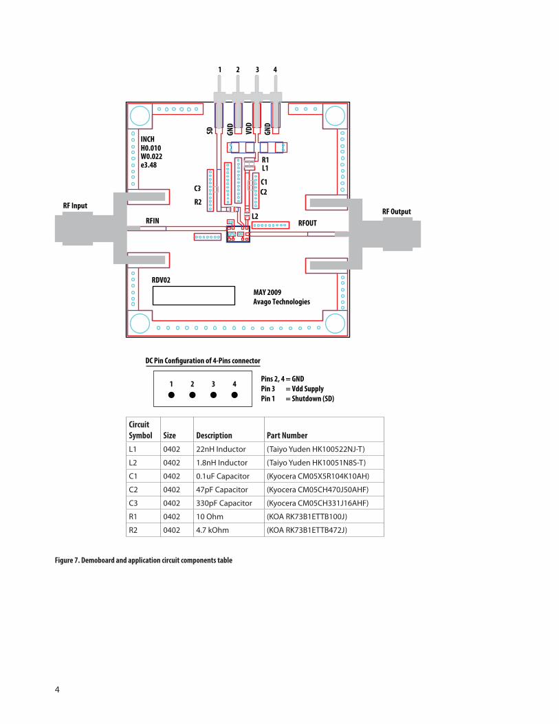
Figure 7. Demoboard and application circuit components table
Pins 2, 4 = GND
Pin 3 = Vdd Supply
Pin 1 = Shutdown (SD)
DC Pin Configuration of 4-Pins connector
1 2 3 4
Circuit
Symbol Size Description Part Number
L1 0402 22nH Inductor (Taiyo Yuden HK100522NJ-T)
L2 0402 1.8nH Inductor (Taiyo Yuden HK10051N8S-T)
C1 0402 0.1uF Capacitor (Kyocera CM05X5R104K10AH)
C2 0402 47pF Capacitor (Kyocera CM05CH470J50AHF)
C3 0402 330pF Capacitor (Kyocera CM05CH331J16AHF)
R1 0402 10 Ohm (KOA RK73B1ETTB100J)
R2 0402 4.7 kOhm (KOA RK73B1ETTB472J)
Avago Technologies
MAY 2009
VD
D
RDV02
SD
RFOUT
H0.010W0.022e3.48
GN
D
INCH
C2
L2RFIN
C3
R2
GN
D
C1
L1R1
1 2 3 4
RF InputRF Output
5
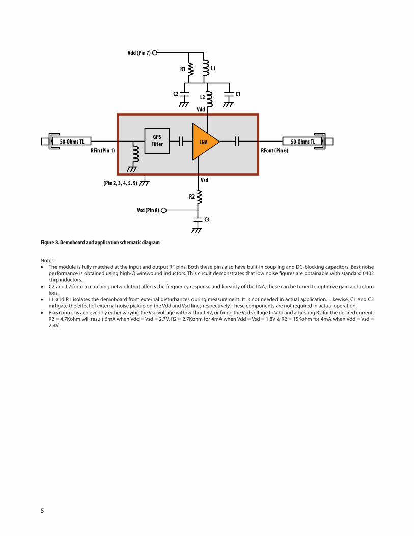
Figure 8. Demoboard and application schematic diagram
Notes�� The module is fully matched at the input and output RF pins. Both these pins also have built-in coupling and DC-blocking capacitors. Best noise
performance is obtained using high-Q wirewound inductors. This circuit demonstrates that low noise figures are obtainable with standard 0402 chip inductors.
�� C2 and L2 form a matching network that affects the frequency response and linearity of the LNA, these can be tuned to optimize gain and return loss.
�� L1 and R1 isolates the demoboard from external disturbances during measurement. It is not needed in actual application. Likewise, C1 and C3 mitigate the effect of external noise pickup on the Vdd and Vsd lines respectively. These components are not required in actual operation.
�� Bias control is achieved by either varying the Vsd voltage with/without R2, or fixing the Vsd voltage to Vdd and adjusting R2 for the desired current.R2 = 4.7Kohm will result 6mA when Vdd = Vsd = 2.7V. R2 = 2.7Kohm for 4mA when Vdd = Vsd = 1.8V & R2 = 15Kohm for 4mA when Vdd = Vsd = 2.8V.
Vsd(Pin 2, 3, 4, 5, 9)
RFin (Pin 1) RFout (Pin 6)
50-Ohms TL 50-Ohms TL
R2
C3
Vsd (Pin 8)
GPSFilter
Vdd
Vdd (Pin 7)
C1L2
C2
R1 L1
LNA
6
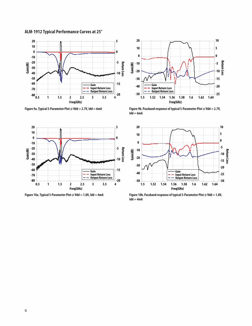
ALM-1912 Typical Performance Curves at 25°
Figure 9a. Typical S-Parameter Plot @ Vdd = 2.7V, Idd = 6mA
Figure 10b. Passband response of typical S-Parameter Plot @ Vdd = 1.8V,
Idd = 4mA
Figure 10a. Typical S-Parameter Plot @ Vdd = 1.8V, Idd = 4mA
Figure 9b. Passband response of typical S-Parameter Plot @ Vdd = 2.7V,
Idd = 6mA
-80
-70
-50
-60
-40
-30
-20
-10
0
10
20
0.5 1 1.5 2 2.5 3 3.5 4
Freq(GHz)
Gai
n(d
B)
-20
-15
-10
-5
0
5
-50
-40
-30
-20
-10
0
10
20
1.5 1.52 1.54 1.56 1.58 1.6 1.62 1.64
Freq(GHz)
Gai
n(d
B)
-25
-20
-15
-10
-5
0
5
10
-80
-70
-60
-50
-40
-30
-20
-10
0
10
20
0.5 1 1.5 2 2.5 3 3.5 4
Freq(GHz)
Gai
n(d
B)
-20
-15
-10
-5
0
5
-50
-40
-30
-20
-10
0
10
20
1.5 1.52 1.54 1.56 1.58 1.6 1.62 1.64
Freq(GHz)
Gai
n(d
B)
-30
-25
-20
-15
-10
-5
0
5
10
Retu
rn Loss
GainInput Return LossOutput Return Loss
GainInput Return LossOutput Return Loss
GainInput Return LossOutput Return Loss
GainInput Return LossOutput Return Loss
Retu
rn Loss
Retu
rn Loss
Retu
rn Loss
7
ALM-1912 Typical Performance Curves at 25°C, R2 = 4.7kOhm
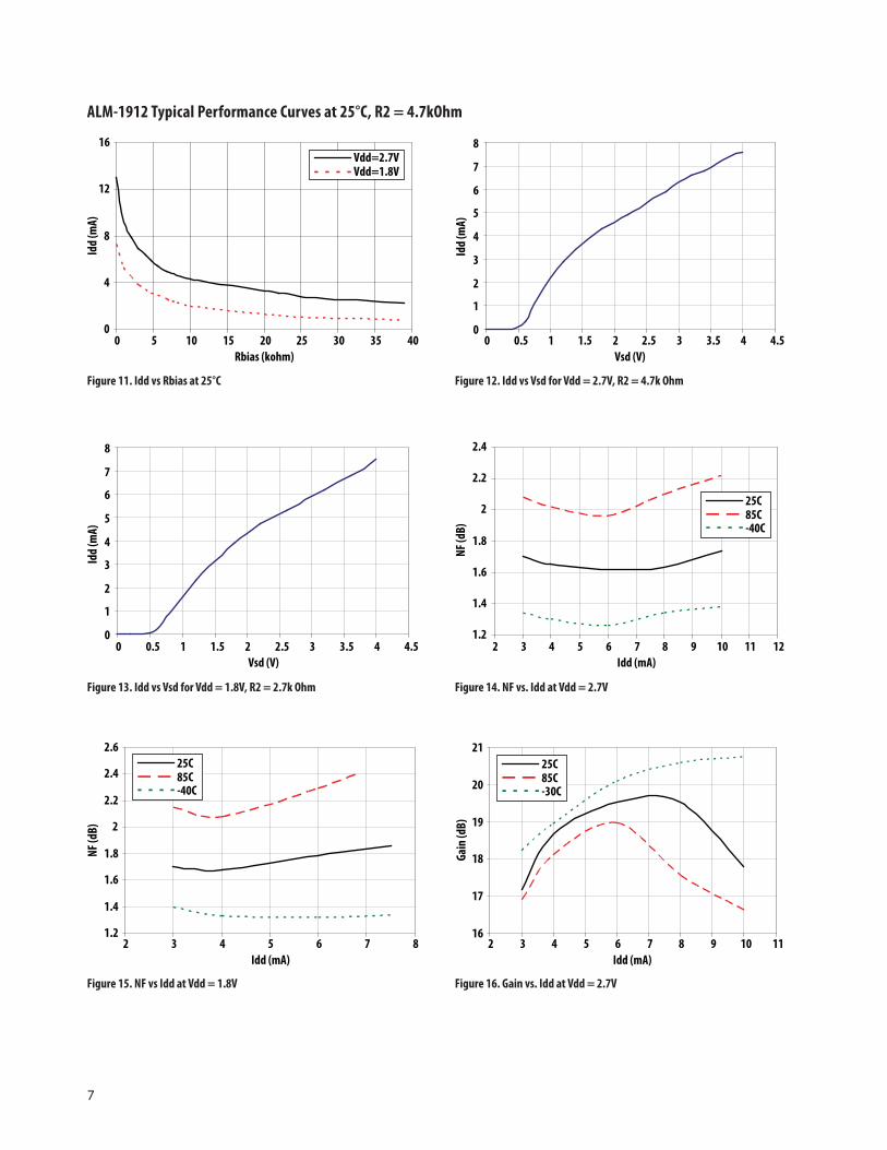
Figure 11. Idd vs Rbias at 25°C
Figure 15. NF vs Idd at Vdd = 1.8V
Figure 14. NF vs. Idd at Vdd = 2.7VFigure 13. Idd vs Vsd for Vdd = 1.8V, R2 = 2.7k Ohm
Figure 12. Idd vs Vsd for Vdd = 2.7V, R2 = 4.7k Ohm
Figure 16. Gain vs. Idd at Vdd = 2.7V
0
4
8
12
16
0 5 10 15 20 25 30 35 40
Rbias (kohm)
Idd
(mA
)
0
1
2
3
4
5
6
7
8
0 0.5 1 1.5 2 2.5 3 3.5 4 4.5
Vsd (V)
Idd
(mA
)
0
1
2
3
4
5
6
7
8
0 0.5 1 1.5 2 2.5 3 3.5 4 4.5
Vsd (V)
Idd
(mA
)
1.2
1.4
1.6
1.8
2
2.2
2.4
2 3 4 5 6 7 8 9 10 11 12
Idd (mA)
NF
(dB
)
1.2
1.4
1.6
1.8
2
2.2
2.4
2.6
2 3 4 5 6 7 8
Idd (mA)
NF
(dB
)
16
17
18
19
20
21
2 3 4 5 6 7 8 9 10 11
Idd (mA)
Gai
n (d
B)
25C85C-40C
25C85C-40C
Vdd=2.7VVdd=1.8V
25C85C-30C
8
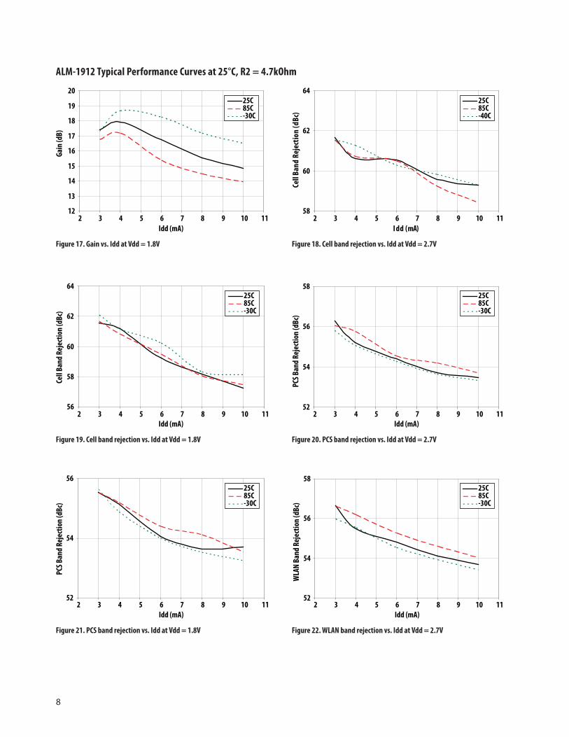
ALM-1912 Typical Performance Curves at 25°C, R2 = 4.7kOhm
Figure 17. Gain vs. Idd at Vdd = 1.8V
Figure 21. PCS band rejection vs. Idd at Vdd = 1.8V
Figure 20. PCS band rejection vs. Idd at Vdd = 2.7VFigure 19. Cell band rejection vs. Idd at Vdd = 1.8V
Figure 18. Cell band rejection vs. Idd at Vdd = 2.7V
Figure 22. WLAN band rejection vs. Idd at Vdd = 2.7V
25C85C-30C
12
13
14
15
16
17
18
19
20
2 3 4 5 6 7 8 9 10 11
Idd (mA)
Gai
n (d
B)
58
60
62
64
2 3 4 5 6 7 8 9 10 11
Idd (mA)
Cell
Ban
d R
ejec
tio
n (
dB
c)
56
58
60
62
64
2 3 4 5 6 7 8 9 10 11
Idd (mA)
Cell
Ban
d R
ejec
tion
(dB
c)
52
54
56
58
2 3 4 5 6 7 8 9 10 11
Idd (mA)
PCS
Ban
d R
ejec
tion
(dB
c)
52
54
56
2 3 4 5 6 7 8 9 10 11
Idd (mA)
PCS
Ban
d R
ejec
tion
(dB
c)
52
54
56
58
2 3 4 5 6 7 8 9 10 11
Idd (mA)
WLA
N B
and
Rej
ecti
on (d
Bc)
25C85C-30C
25C85C-30C
25C85C-30C
25C85C-30C
25C85C-40C
9
ALM-1912 Typical Performance Curves at 25°C, R2 = 4.7kOhm
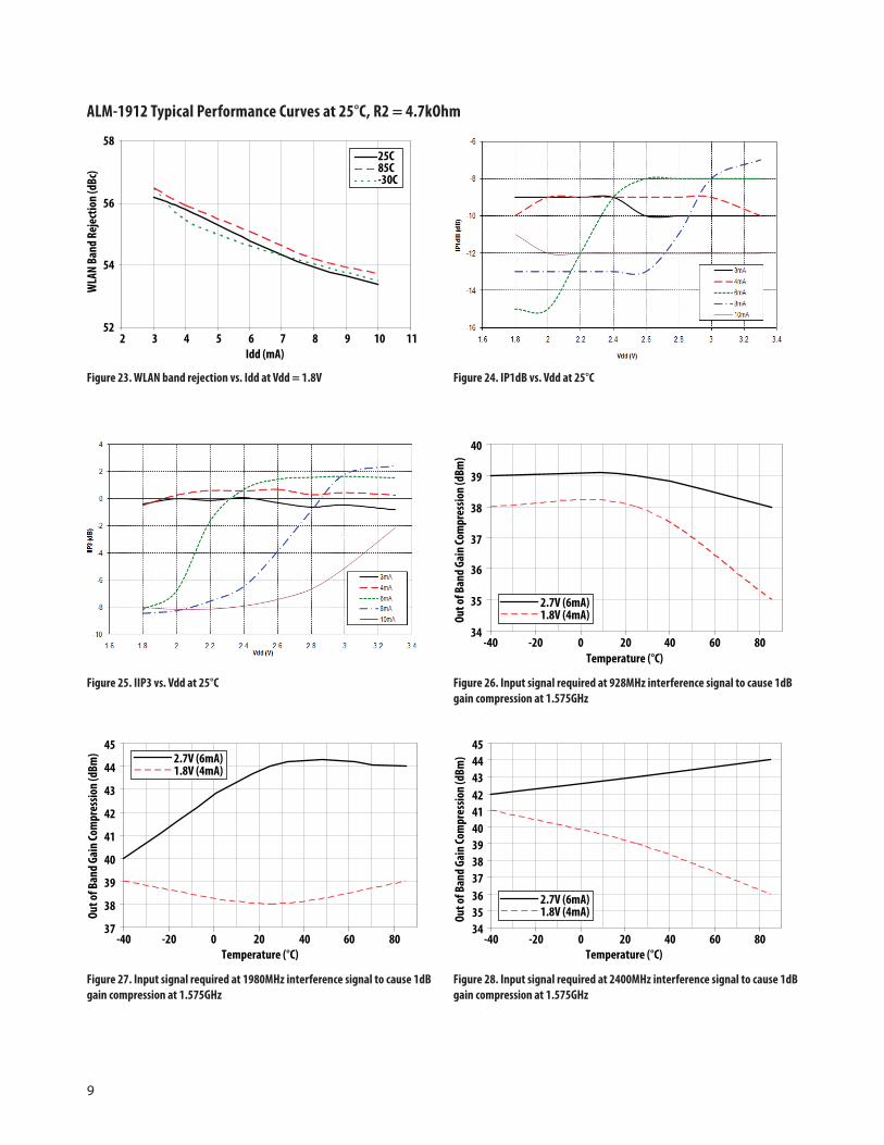
Figure 23. WLAN band rejection vs. Idd at Vdd = 1.8V
Figure 27. Input signal required at 1980MHz interference signal to cause 1dB
gain compression at 1.575GHz
Figure 26. Input signal required at 928MHz interference signal to cause 1dB
gain compression at 1.575GHz
Figure 25. IIP3 vs. Vdd at 25°C
Figure 24. IP1dB vs. Vdd at 25°C
Figure 28. Input signal required at 2400MHz interference signal to cause 1dB
gain compression at 1.575GHz
52
54
56
58
2 3 4 5 6 7 8 9 10 11
Idd (mA)
WLA
N B
and
Rej
ecti
on (d
Bc)
37
38
39
40
41
42
43
44
45
-40 -20 0 20 40 60 80
Ou
t of
Ban
d G
ain
Com
pres
sion
(dB
m)
34
35
36
37
38
39
40
41
42
43
44
45
-40 -20 0 20 40 60 80
Temperature (°C)
Ou
t of
Ban
d G
ain
Com
pres
sion
(dB
m)
34
35
36
37
38
39
40
-40 -20 0 20 40 60 80
Temperature (°C)
Ou
t of
Ban
d G
ain
Com
pres
sion
(dB
m)
25C85C-30C
2.7V (6mA)1.8V (4mA)
2.7V (6mA)1.8V (4mA)
2.7V (6mA)1.8V (4mA)
Temperature (°C)
10
ALM-1912 Typical Performance Curves at 25°C, R2 = 4.7kOhm
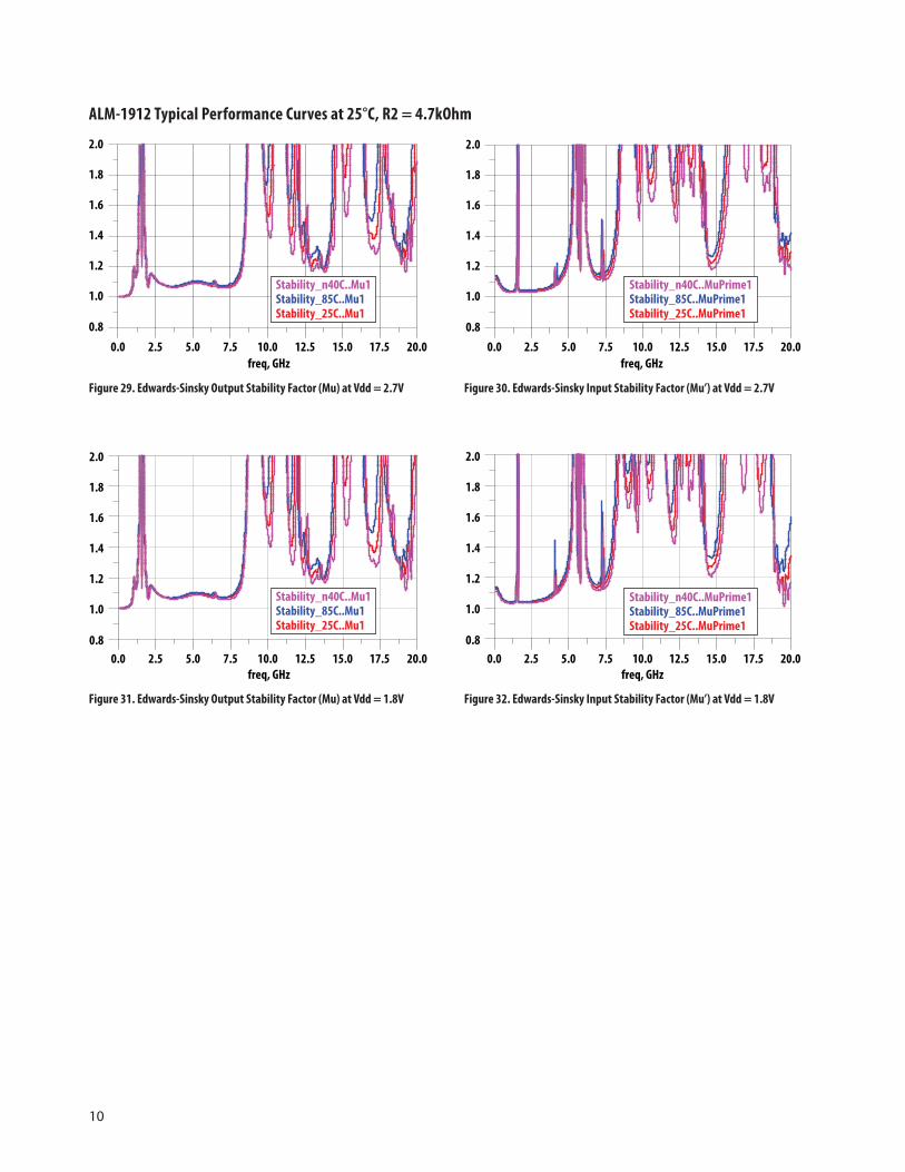
Figure 29. Edwards-Sinsky Output Stability Factor (Mu) at Vdd = 2.7V
Figure 32. Edwards-Sinsky Input Stability Factor (Mu’) at Vdd = 1.8VFigure 31. Edwards-Sinsky Output Stability Factor (Mu) at Vdd = 1.8V
Figure 30. Edwards-Sinsky Input Stability Factor (Mu’) at Vdd = 2.7V
2.5 5.0 7.5 10.0 12.5 15.0 17.50.0 20.0
1.0
1.2
1.4
1.6
1.8
0.8
2.0
freq, GHz
Stability_25C..Mu1Stability_85C..Mu1Stability_n40C..Mu1
2.5 5.0 7.5 10.0 12.5 15.0 17.50.0 20.0
1.0
1.2
1.4
1.6
1.8
0.8
2.0
freq, GHz
2.5 5.0 7.5 10.0 12.5 15.0 17.50.0 20.0
1.0
1.2
1.4
1.6
1.8
0.8
2.0
freq, GHz
2.5 5.0 7.5 10.0 12.5 15.0 17.50.0 20.0
1.0
1.2
1.4
1.6
1.8
0.8
2.0
freq, GHz
Stability_25C..MuPrime1Stability_85C..MuPrime1Stability_n40C..MuPrime1
Stability_25C..MuPrime1Stability_85C..MuPrime1Stability_n40C..MuPrime1
Stability_25C..Mu1Stability_85C..Mu1Stability_n40C..Mu1
11
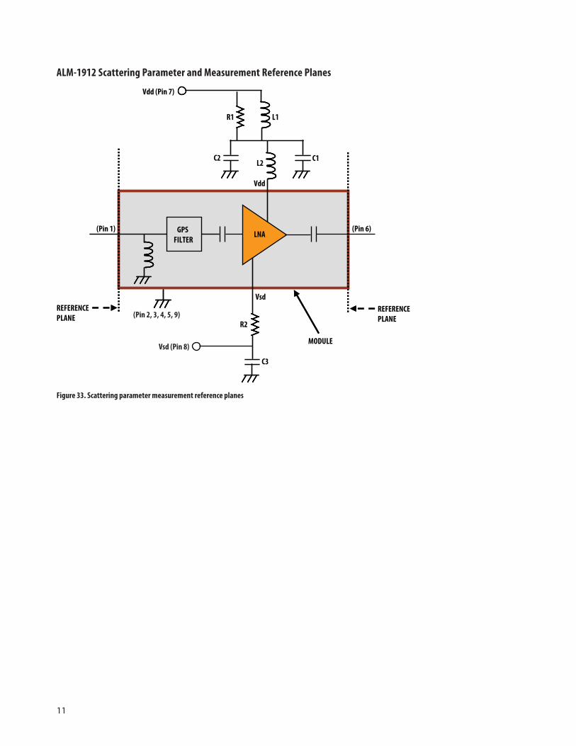
ALM-1912 Scattering Parameter and Measurement Reference Planes
Figure 33. Scattering parameter measurement reference planes
Vsd
(Pin 6)
Vdd
C1L2
C2
R1 L1
R2
C3
(Pin 1) GPS
FILTER
MODULE
REFERENCE
PLANE
LNA
REFERENCE
PLANE
Vdd (Pin 7)
(Pin 2, 3, 4, 5, 9)
Vsd (Pin 8)
12
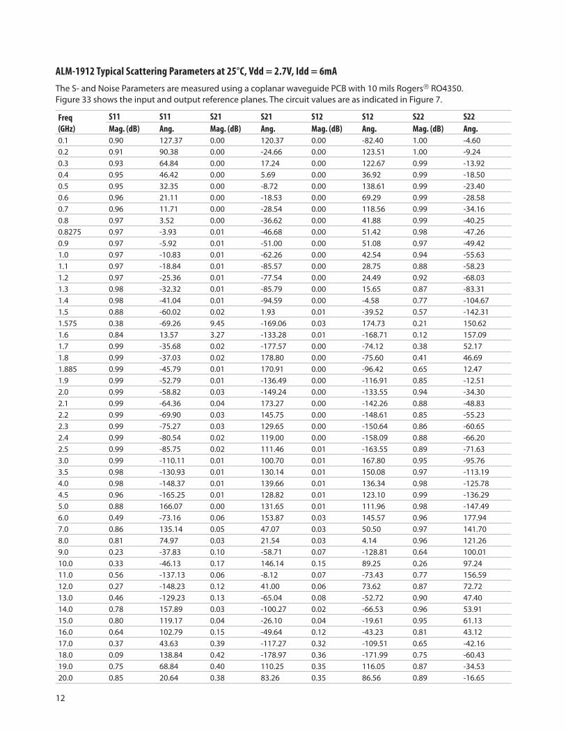
ALM-1912 Typical Scattering Parameters at 25°C, Vdd = 2.7V, Idd = 6mA
The S- and Noise Parameters are measured using a coplanar waveguide PCB with 10 mils Rogers� RO4350. Figure 33 shows the input and output reference planes. The circuit values are as indicated in Figure 7.
Freq
(GHz)
S11 S11 S21 S21 S12 S12 S22 S22
Mag. (dB) Ang. Mag. (dB) Ang. Mag. (dB) Ang. Mag. (dB) Ang.
0.1 0.90 127.37 0.00 120.37 0.00 -82.40 1.00 -4.600.2 0.91 90.38 0.00 -24.66 0.00 123.51 1.00 -9.240.3 0.93 64.84 0.00 17.24 0.00 122.67 0.99 -13.920.4 0.95 46.42 0.00 5.69 0.00 36.92 0.99 -18.500.5 0.95 32.35 0.00 -8.72 0.00 138.61 0.99 -23.400.6 0.96 21.11 0.00 -18.53 0.00 69.29 0.99 -28.580.7 0.96 11.71 0.00 -28.54 0.00 118.56 0.99 -34.160.8 0.97 3.52 0.00 -36.62 0.00 41.88 0.99 -40.250.8275 0.97 -3.93 0.01 -46.68 0.00 51.42 0.98 -47.260.9 0.97 -5.92 0.01 -51.00 0.00 51.08 0.97 -49.421.0 0.97 -10.83 0.01 -62.26 0.00 42.54 0.94 -55.631.1 0.97 -18.84 0.01 -85.57 0.00 28.75 0.88 -58.231.2 0.97 -25.36 0.01 -77.54 0.00 24.49 0.92 -68.031.3 0.98 -32.32 0.01 -85.79 0.00 15.65 0.87 -83.311.4 0.98 -41.04 0.01 -94.59 0.00 -4.58 0.77 -104.671.5 0.88 -60.02 0.02 1.93 0.01 -39.52 0.57 -142.311.575 0.38 -69.26 9.45 -169.06 0.03 174.73 0.21 150.621.6 0.84 13.57 3.27 -133.28 0.01 -168.71 0.12 157.091.7 0.99 -35.68 0.02 -177.57 0.00 -74.12 0.38 52.171.8 0.99 -37.03 0.02 178.80 0.00 -75.60 0.41 46.691.885 0.99 -45.79 0.01 170.91 0.00 -96.42 0.65 12.471.9 0.99 -52.79 0.01 -136.49 0.00 -116.91 0.85 -12.512.0 0.99 -58.82 0.03 -149.24 0.00 -133.55 0.94 -34.302.1 0.99 -64.36 0.04 173.27 0.00 -142.26 0.88 -48.832.2 0.99 -69.90 0.03 145.75 0.00 -148.61 0.85 -55.232.3 0.99 -75.27 0.03 129.65 0.00 -150.64 0.86 -60.652.4 0.99 -80.54 0.02 119.00 0.00 -158.09 0.88 -66.202.5 0.99 -85.75 0.02 111.46 0.01 -163.55 0.89 -71.633.0 0.99 -110.11 0.01 100.70 0.01 167.80 0.95 -95.763.5 0.98 -130.93 0.01 130.14 0.01 150.08 0.97 -113.194.0 0.98 -148.37 0.01 139.66 0.01 136.34 0.98 -125.784.5 0.96 -165.25 0.01 128.82 0.01 123.10 0.99 -136.295.0 0.88 166.07 0.00 131.65 0.01 111.96 0.98 -147.496.0 0.49 -73.16 0.06 153.87 0.03 145.57 0.96 177.947.0 0.86 135.14 0.05 47.07 0.03 50.50 0.97 141.708.0 0.81 74.97 0.03 21.54 0.03 4.14 0.96 121.269.0 0.23 -37.83 0.10 -58.71 0.07 -128.81 0.64 100.0110.0 0.33 -46.13 0.17 146.14 0.15 89.25 0.26 97.2411.0 0.56 -137.13 0.06 -8.12 0.07 -73.43 0.77 156.5912.0 0.27 -148.23 0.12 41.00 0.06 73.62 0.87 72.7213.0 0.46 -129.23 0.13 -65.04 0.08 -52.72 0.90 47.4014.0 0.78 157.89 0.03 -100.27 0.02 -66.53 0.96 53.9115.0 0.80 119.17 0.04 -26.10 0.04 -19.61 0.95 61.1316.0 0.64 102.79 0.15 -49.64 0.12 -43.23 0.81 43.1217.0 0.37 43.63 0.39 -117.27 0.32 -109.51 0.65 -42.1618.0 0.09 138.84 0.42 -178.97 0.36 -171.99 0.75 -60.4319.0 0.75 68.84 0.40 110.25 0.35 116.05 0.87 -34.5320.0 0.85 20.64 0.38 83.26 0.35 86.56 0.89 -16.65
13
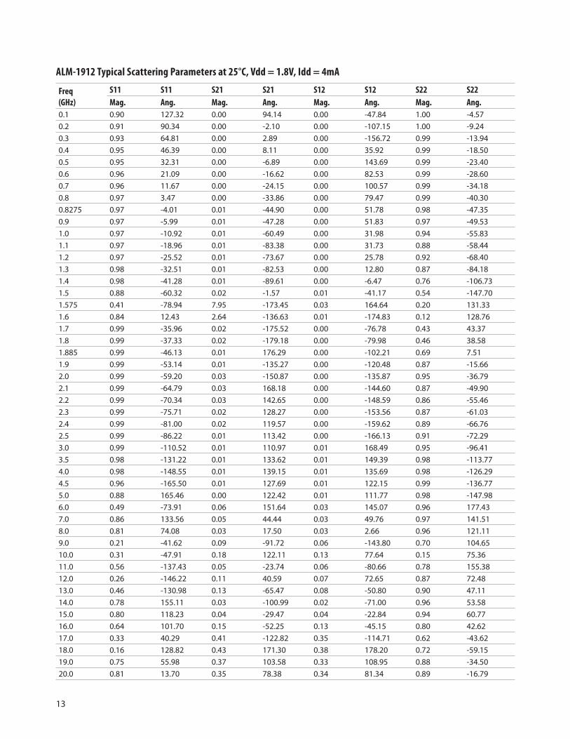
ALM-1912 Typical Scattering Parameters at 25°C, Vdd = 1.8V, Idd = 4mA
Freq
(GHz)
S11 S11 S21 S21 S12 S12 S22 S22
Mag. Ang. Mag. Ang. Mag. Ang. Mag. Ang.
0.1 0.90 127.32 0.00 94.14 0.00 -47.84 1.00 -4.57
0.2 0.91 90.34 0.00 -2.10 0.00 -107.15 1.00 -9.24
0.3 0.93 64.81 0.00 2.89 0.00 -156.72 0.99 -13.94
0.4 0.95 46.39 0.00 8.11 0.00 35.92 0.99 -18.50
0.5 0.95 32.31 0.00 -6.89 0.00 143.69 0.99 -23.40
0.6 0.96 21.09 0.00 -16.62 0.00 82.53 0.99 -28.60
0.7 0.96 11.67 0.00 -24.15 0.00 100.57 0.99 -34.18
0.8 0.97 3.47 0.00 -33.86 0.00 79.47 0.99 -40.30
0.8275 0.97 -4.01 0.01 -44.90 0.00 51.78 0.98 -47.35
0.9 0.97 -5.99 0.01 -47.28 0.00 51.83 0.97 -49.53
1.0 0.97 -10.92 0.01 -60.49 0.00 31.98 0.94 -55.83
1.1 0.97 -18.96 0.01 -83.38 0.00 31.73 0.88 -58.44
1.2 0.97 -25.52 0.01 -73.67 0.00 25.78 0.92 -68.40
1.3 0.98 -32.51 0.01 -82.53 0.00 12.80 0.87 -84.18
1.4 0.98 -41.28 0.01 -89.61 0.00 -6.47 0.76 -106.73
1.5 0.88 -60.32 0.02 -1.57 0.01 -41.17 0.54 -147.70
1.575 0.41 -78.94 7.95 -173.45 0.03 164.64 0.20 131.33
1.6 0.84 12.43 2.64 -136.63 0.01 -174.83 0.12 128.76
1.7 0.99 -35.96 0.02 -175.52 0.00 -76.78 0.43 43.37
1.8 0.99 -37.33 0.02 -179.18 0.00 -79.98 0.46 38.58
1.885 0.99 -46.13 0.01 176.29 0.00 -102.21 0.69 7.51
1.9 0.99 -53.14 0.01 -135.27 0.00 -120.48 0.87 -15.66
2.0 0.99 -59.20 0.03 -150.87 0.00 -135.87 0.95 -36.79
2.1 0.99 -64.79 0.03 168.18 0.00 -144.60 0.87 -49.90
2.2 0.99 -70.34 0.03 142.65 0.00 -148.59 0.86 -55.46
2.3 0.99 -75.71 0.02 128.27 0.00 -153.56 0.87 -61.03
2.4 0.99 -81.00 0.02 119.57 0.00 -159.62 0.89 -66.76
2.5 0.99 -86.22 0.01 113.42 0.00 -166.13 0.91 -72.29
3.0 0.99 -110.52 0.01 110.97 0.01 168.49 0.95 -96.41
3.5 0.98 -131.22 0.01 133.62 0.01 149.39 0.98 -113.77
4.0 0.98 -148.55 0.01 139.15 0.01 135.69 0.98 -126.29
4.5 0.96 -165.50 0.01 127.69 0.01 122.15 0.99 -136.77
5.0 0.88 165.46 0.00 122.42 0.01 111.77 0.98 -147.98
6.0 0.49 -73.91 0.06 151.64 0.03 145.07 0.96 177.43
7.0 0.86 133.56 0.05 44.44 0.03 49.76 0.97 141.51
8.0 0.81 74.08 0.03 17.50 0.03 2.66 0.96 121.11
9.0 0.21 -41.62 0.09 -91.72 0.06 -143.80 0.70 104.65
10.0 0.31 -47.91 0.18 122.11 0.13 77.64 0.15 75.36
11.0 0.56 -137.43 0.05 -23.74 0.06 -80.66 0.78 155.38
12.0 0.26 -146.22 0.11 40.59 0.07 72.65 0.87 72.48
13.0 0.46 -130.98 0.13 -65.47 0.08 -50.80 0.90 47.11
14.0 0.78 155.11 0.03 -100.99 0.02 -71.00 0.96 53.58
15.0 0.80 118.23 0.04 -29.47 0.04 -22.84 0.94 60.77
16.0 0.64 101.70 0.15 -52.25 0.13 -45.15 0.80 42.62
17.0 0.33 40.29 0.41 -122.82 0.35 -114.71 0.62 -43.62
18.0 0.16 128.82 0.43 171.30 0.38 178.20 0.72 -59.15
19.0 0.75 55.98 0.37 103.58 0.33 108.95 0.88 -34.50
20.0 0.81 13.70 0.35 78.38 0.34 81.34 0.89 -16.79
14
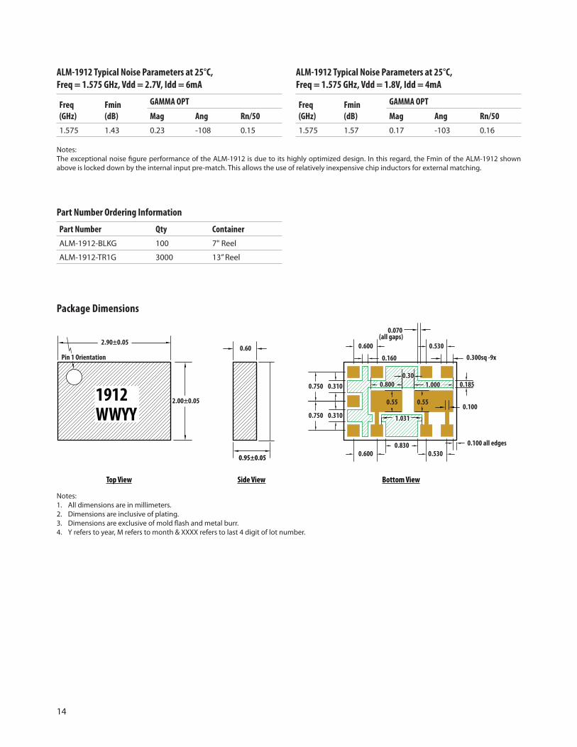
ALM-1912 Typical Noise Parameters at 25°C,
Freq = 1.575 GHz, Vdd = 2.7V, Idd = 6mA
Freq
(GHz)
Fmin
(dB)
GAMMA OPT
Mag Ang Rn/50
1.575 1.43 0.23 -108 0.15
ALM-1912 Typical Noise Parameters at 25°C,
Freq = 1.575 GHz, Vdd = 1.8V, Idd = 4mA
Freq
(GHz)
Fmin
(dB)
GAMMA OPT
Mag Ang Rn/50
1.575 1.57 0.17 -103 0.16
Notes:The exceptional noise figure performance of the ALM-1912 is due to its highly optimized design. In this regard, the Fmin of the ALM-1912 shown above is locked down by the internal input pre-match. This allows the use of relatively inexpensive chip inductors for external matching.
Part Number Ordering Information
Part Number Qty Container
ALM-1912-BLKG 100 7" Reel
ALM-1912-TR1G 3000 13” Reel
Package Dimensions
Notes:1. All dimensions are in millimeters.2. Dimensions are inclusive of plating.3. Dimensions are exclusive of mold flash and metal burr.4. Y refers to year, M refers to month & XXXX refers to last 4 digit of lot number.
Top View Side View Bottom View
Pin 1 Orientation
0.600 0.530
0.600 0.530
0.750
0.750
0.160
0.1850.310
0.310
0.830 0.100 all edges
0.800
0.55
1.000
0.55
0.300sq -9x
0.100
1.031
0.070(all gaps)
0.30
0.602.90±0.05
2.00±0.05
0.95±0.05
1912WWYY
15
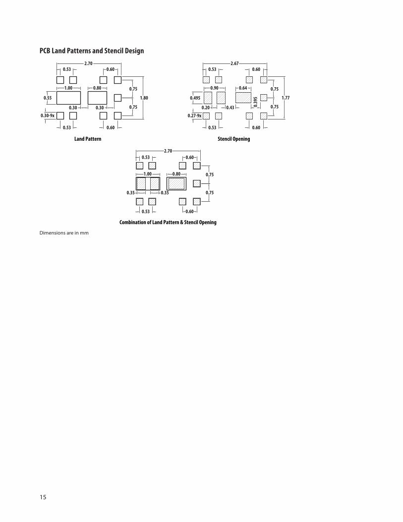
PCB Land Patterns and Stencil Design
Land Pattern Stencil Opening
Combination of Land Pattern & Stencil Opening
0.53 0.60
0.53 0.60
0.801.00
0.75
0.75
0.30 0.30
2.70
1.800.55
2.670.53 0.60
1.77
0.75
0.75
0.90 0.64
0.430.20 0.39
5
0.600.53
0.495
2.70
0.53 0.60
0.30-9x
0.75
0.75
0.600.53
0.27-9x
1.00 0.80
0.35 0.35
Dimensions are in mm
16
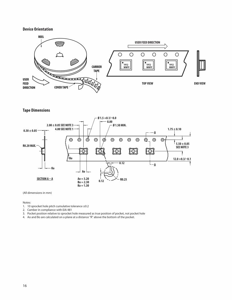
Device Orientation
Tape Dimensions
Notes:1. 10 sprocket hole pitch cumulative tolerance ±0.22. Camber in compliance with EIA 4813. Pocket position relative to sprocket hole measured as true position of pocket, not pocket hole4. Ao and Bo are calculated on a plane at a distance "R" above the bottom of the pocket.
USER FEED DIRECTION
TOP VIEW END VIEW
USER
FEED
DIRECTION COVER TAPE
CARRIER
TAPE
REEL
1912WWYY
1912WWYY
1912WWYY
0.30 ± 0.05
R0.20 MAX.
2.00 ± 0.05 SEE NOTE 3
4.00 SEE NOTE 1
Ø 1.5 +0.1/0.0
Ø 1.50 MIN.8.00
1.75 ± 0.10
5.50 ± 0.05 SEE NOTE 3
A
A
12.0 +0.3/0.1Bo
Ao
0.12
0.12 R0.25
Ko
SECTION A A Ao = 3.20Bo = 2.30Ko = 1.30
(All dimensions in mm)
For product information and a complete list of distributors, please go to our web site: www.avagotech.com
Avago, Avago Technologies, and the A logo are trademarks of Avago Technologies in the United States and other countries.
Data subject to change. Copyright © 2005-2010 Avago Technologies. All rights reserved.
AV02-2218EN - March 26, 2010
Reel Dimensions - 13 Inch x 12mm
PS
6
211211
109
8 7
20
3
54
6
6PS
PS
6
CPN
12MM
MPN
Detail "X"
RECYCLE LOGO
SEE DETAIL "X"
R19.0±0.5
Ø12.3±0.5(3x)
Ø10
0.0±
0.5
Ø32
9.0±
1.0
11.9-15.4**
18.4 MAX.*
SLOT
5.0±0.5(3x)
12.4+2.0*
-0.0
16.0mm HEIGHT x MIN. 0.4mm THICK.
EMBOSSED LETTERING
EMBOSSED LINE (2x)
89.0mm LENGTH LINES 147.0mm
AWAY FROM CENTER POINT
7.5mm HEIGHT EMBOSSED LETTERING
DATE CODE
ESD LOGO
Ø16.0
7.5mm HEIGHT
EMBOSSED LETTERING
HUB
Ø100.0±0.5
Ø329.0±1.0
20.2(MIN.)
1.5(
MIN
.)
Ø13.0-0.2
+0.5
BACK VIEW
FRONT VIEW
20
12
10
87
11
9
1
3
4
65
2