Embed Size (px)
Citation preview
Order this documentby MC68HC11FTS/D
F
ree
sca
le S
em
ico
nd
uc
tor,
I
nc
...
ATAMC68HC11F1
MC68HC11FC0Technical Summary8-Bit Microcontroller
1 IntroductionThe MC68HC11F1 is a high-performance member of the M68HC11 family of microcontroller units(MCUs). High-speed expanded systems required the development of this chip with its extra input/output(I/O) ports, an increase in static RAM (one Kbyte), internal chip-select functions, and a non-multiplexedbus which reduces the need for external interface logic. The timer, serial I/O, and analog-to-digital (A/D) converter enable functions similar to those found in the MC68HC11E9.
The MC68HC11FC0 is a low cost, high-speed derivative of the MC68HC11F1. It does not haveEEPROM or an analog-to-digital converter. The MC68HC11FC0 can operate at bus speeds as high assix MHz.
This document provides a brief overview of the structure, features, control registers, packaging infor-mation and availability of the MC68HC11F1 and MC68HC11FC0. For detailed information onM68HC11 subsystems, programming and the instruction set, refer to the M68HC11 Reference Manual(M68HC11RM/AD).
1.1 Features• MC68HC11 CPU• 512 Bytes of On-Chip Electrically Erasable Programmable ROM (EEPROM) with Block Protect
(MC68HC11F1 only)• 1024 Bytes of On-Chip RAM (All Saved During Standby)• Enhanced 16-Bit Timer System
— 3 Input Capture (IC) Functions— 4 Output Compare (OC) Functions— 4th IC or 5th OC (Software Selectable)
• On-Board Chip-Selects with Clock Stretching• Real-Time Interrupt Circuit• 8-Bit Pulse Accumulator• Synchronous Serial Peripheral Interface (SPI)• Asynchronous Nonreturn to Zero (NRZ) Serial Communication Interface (SCI)• Power saving STOP and WAIT Modes• Eight-Channel 8-Bit A/D Converter (MC68HC11F1 only)• Computer Operating Properly (COP) Watchdog System and Clock Monitor• Bus Speeds of up to 6 MHz for the MC68HC11FC0 and up to 5 MHz for the MC68HC11F1• 68-Pin PLCC (MC68HC11F1 only), 64-Pin QFP (MC68HC11FC0 only), and 80-pin TQFP pack-
age options
© MOTOROLA INC., 1997
This document contains information on a new product. Specifications and information herein are subject to change without notice.
M

Fre
esc
ale
Se
mic
on
du
cto
r, I
Freescale Semiconductor, Inc.n
c..
.
1.2 Ordering Information
The following devices all have 1024 bytes of RAM. In addition, the MC68HC11F1 devices have 512bytes of EEPROM. None of the devices contain on-chip ROM.
Table 1 MC68HC11F1 Standard Device Ordering Information
Package Temperature Frequency MC Order Number
80-Pin Thin Quad Flat Pack (TQFP)
(14 mm X 14 mm,1.4 mm thick)
0° to +70° 5 MHz MC68HC11F1PU5
-40° to +85°C
2 MHz MC68HC11F1CPU2
3 MHz MC68HC11F1CPU3
4 MHz MC68HC11F1CPU4
5 MHz MC68HC11F1CPU5
– 40° to + 105° C
2 MHz MC68HC11F1VPU2
3 MHz MC68HC11F1VPU3
4 MHz MC68HC11F1VPU4
– 40° to + 125° C
2 MHz MC68HC11F1MPU2
3 MHz MC68HC11F1MPU3
4 MHz MC68HC11F1MPU4
68-Pin PLCC
0° to +70° 5 MHz MC68HC11F1FN5
– 40° to + 85° C
2 MHz MC68HC11F1CFN2
3 MHz MC68HC11F1CFN3
4 MHz MC68HC11F1CFN4
5 MHz MC68HC11F1CFN5
– 40° to + 105° C
2 MHz MC68HC11F1VFN2
3 MHz MC68HC11F1VFN3
4 MHz MC68HC11F1VFN4
– 40° to + 125° C
2 MHz MC68HC11F1MFN2
3 MHz MC68HC11F1MFN3
4 MHz MC68HC11F1MFN4
Table 2 MC68HC11F1 Extended Voltage (3.0 to 5.5 V) Device Ordering Information
Package Temperature Frequency MC Order Number
68-Pin Plastic Leaded Chip Carrier (PLCC)
0° to +70°C 3 MHz MC68L11F1FN3
–40° to +85°C 3 MHz MC68L11F1CFN3
80-Pin Thin Quad Flat Pack (TQFP)
0° to +70°C 3 MHz MC68L11F1PU3
–40° to +85°C 3 MHz MC68L11F1CPU3
MC68HC11F1/FC02 MC68HC11FTS/D
For More Information On This Product,
Go to: www.freescale.com

Fre
esc
ale
Se
mic
on
du
cto
r, I
Freescale Semiconductor, Inc.n
c..
.
Table 3 MC68HC11FC0 Standard Device Ordering Information
Package Temperature Frequency MC Order Number
64-Pin Quad Flat Pack(QFP)
–40° to +85°C4 MHz MC68HC11FC0CFU4
5 MHz MC68HC11FC0CFU5
0° to 70° C 6 MHz MC68HC11FC0FU6
80-Pin Thin Quad Flat Pack (TQFP)
–40° to +85°C4 MHz MC68HC11FC0CPU4
5 MHz MC68HC11FC0CPU5
0° to 70° C 6 MHz MC68HC11FC0PU6
Table 4 MC68HC11FC0 Extended Voltage (3.0 to 5.5 V) Device Ordering Information
Package Temperature Frequency MC Order Number
64-Pin Quad Flat Pack(QFP)
–0° to +70°C
3 MHz MC68L11FC0FU3
4 MHz MC68L11FC0FU4
80-Pin Thin Quad Flat Pack (TQFP)
3 MHz MC68L11FC0PU3
4 MHz MC68L11FC0PU4
MC68HC11F1/FC0 MC68HC11FTS/D 3
For More Information On This Product,
Go to: www.freescale.com

Section Page
MC68HC11F1/FC04 MC68HC11FTS/D
1 Introduction
1
1.1 Features ......................................................................................................................................11.2 Ordering Information ...................................................................................................................21.3 Block Diagrams ..........................................................................................................................6
2 Pin Assignments and Signal Descriptions
8
2.1 MC68HC11F1 Pin Assignments ..................................................................................................82.2 MC68HC11FC0 Pin Assignments .............................................................................................102.3 Pin Descriptions ........................................................................................................................12
3 Control Registers
14
3.1 MC68HC11F1 Control Registers ...............................................................................................143.2 MC68HC11FC0 Control Registers ............................................................................................16
4 Operating Modes and System Initialization
18
4.1 Operating Modes .......................................................................................................................184.2 Memory Maps ............................................................................................................................194.3 System Initialization Registers ..................................................................................................20
5 Resets and Interrupts
25
5.1 Interrupt Sources .......................................................................................................................255.2 Reset and Interrupt Registers ...................................................................................................26
6 Electrically Erasable Programmable ROM
29
6.1 EEPROM Operation ..................................................................................................................296.2 EEPROM Registers ...................................................................................................................296.3 EEPROM Programming and Erasure ........................................................................................316.4 CONFIG Register Programming ...............................................................................................32
7 Parallel Input/Output
33
7.1 Port A ........................................................................................................................................337.2 Port B ........................................................................................................................................337.3 Port C ........................................................................................................................................337.4 Port D ........................................................................................................................................337.5 Port E ........................................................................................................................................337.6 Port F .........................................................................................................................................337.7 Port G ........................................................................................................................................347.8 Parallel I/O Registers ................................................................................................................34
8 Chip-Selects
38
8.1 Chip-Select Operation ...............................................................................................................388.2 Chip-Select Registers ................................................................................................................38
9 Serial Communications Interface (SCI)
42
9.1 SCI Block Diagrams ..................................................................................................................429.2 SCI Registers ............................................................................................................................44
10 Serial Peripheral Interface
49
10.1 SPI Block Diagram ....................................................................................................................4910.2 SPI Registers ............................................................................................................................50
11 Analog-to-Digital Converter
53
11.1 Input Pins ..................................................................................................................................5411.2 Conversion Sequence ...............................................................................................................5411.3 A/D Registers ............................................................................................................................55
12 Main Timer
57
12.1 Timer Operation ........................................................................................................................5712.2 Timer Registers .........................................................................................................................59
13 Pulse Accumulator
64
13.1 Pulse Accumulator Block Diagram ............................................................................................6413.2 Pulse Accumulator Registers ....................................................................................................64
TABLE OF CONTENTS
Fre
esc
ale
Se
mic
on
du
cto
r, I
Freescale Semiconductor, Inc.
For More Information On This Product, Go to: www.freescale.com
nc
...

Register Address Page
MC68HC11F1/FC0 MC68HC11FTS/D 5
ADCTL ................ A/D Control/Status .........................................................$1030
..........................55BAUD .................. Baud Rate......................................................................$102B
..........................44BPROT................ Block Protect..................................................................$1035
..........................29CFORC ............... Timer Force Compare....................................................$100B
..........................59CONFIG .............. EEPROM Mapping, COP, EEPROM Enables ...............$103F
............. 24
,
28
,
30COPRST ............. Arm/Reset COP Timer Circuitry.....................................$103A
..........................27CSCTL ................ Chip-Select Control........................................................$105D
..........................39CSGADR............. General-Purpose Chip-Select Address Register ........... $105E
.........................40CSGSIZ............... General-Purpose Chip-Select Size Register ................$105F
..........................40CSSTRH ............. Clock Stretching.............................................................$105C
..........................38DDRA.................. Port A Data Register......................................................$1001
..........................34DDRC.................. Data Direction Register for Port C .................................$1007
..........................35DDRD.................. Data Direction Register for Port D .................................$1009
..........................36DDRG.................. Data Direction Register for Port G.................................$1003
..........................35HPRIO................. Highest Priority Interrupt and Miscellaneous ................$103C
................... 20
,
27INIT ..................... RAM and I/O Mapping ...................................................$103D
................... 21
,
22OC1D .................. Output Compare 1 Data ................................................$100D
..........................59OC1M.................. Output Compare 1 Mask ...............................................$100C
..........................59OPT2................... System Configuration Option Register 2 .......................$1038
............. 22
,
36
,
52OPTION .............. System Configuration Options.......................................$1039
............. 23
,
26
,
56PACNT................ Pulse Accumulator Count ..............................................$1027
..........................66PACTL................. Pulse Accumulator Control ...........................................$1026
................... 63
,
65PORTA................ Port A Data ....................................................................$1000
..........................34PORTB................ Port B Data ....................................................................$1004 ..........................35PORTC................ Port C Data ....................................................................$1006 ..........................35PORTD................ Port D Data ....................................................................$1008 ..........................36PORTE................ Port E Data ....................................................................$100A ..........................36PORTF................ Port F Data ....................................................................$1005 ..........................35PORTG ............... Port G Data....................................................................$1002 ..........................34PPROG ............... EEPROM Programming Control ....................................$103B ..........................30SCCR1................ SCI Control 1 ................................................................$102C ..........................46SCCR2................ SCI Control 2 ................................................................$102D ..........................46SCDR.................. Serial Communications Data Register...........................$102F ..........................48SCSR .................. SCI Status......................................................................$102E ..........................47SPCR .................. Serial Peripheral Control ...............................................$1028 ..........................50SPDR .................. SPI Data .......................................................................$102A ..........................51SPSR .................. Serial Peripheral Status .................................................$1029 ..........................51TCNT................... Timer Count ..................................................................$100E, $100F ..............59TCTL1 ................. Timer Control 1 ..............................................................$1020 ..........................60TCTL2 ................. Timer Control 2 ..............................................................$1021 ..........................61TEST1................. Factory Test ..................................................................$103E ..........................24TFLG1................. Timer Interrupt Flag 1 ...................................................$1023 ..........................61TFLG2................. Timer Interrupt Flag 2 ...................................................$1025 ................... 62, 65TI4O5 .................. Timer Input Capture 4/Output Compare 5 ....................$101E, $101F ..............60TIC1–TIC3........... Timer Input Capture ......................................................$1010–$1015 ..............60TMSK1 ................ Timer Interrupt Mask 1 ..................................................$1022 ..........................61TMSK2 ................ Timer Interrupt Mask 2 ..................................................$1024 ................... 62, 64TOC1–TOC4....... Timer Output Compare .................................................$1016–$101D ..............60
REGISTER INDEX
Fre
esc
ale
Se
mic
on
du
cto
r, I
Freescale Semiconductor, Inc.
For More Information On This Product, Go to: www.freescale.com
nc
...

F
ree
sca
le S
em
ico
nd
uc
tor,
I
Freescale Semiconductor, Inc.n
c..
.
1.3 Block Diagrams
Figure 1 MC68HC11F1 Block Diagram
POWERCLOCKLOGIC
INTERRUPTLOGIC
MODECONTROL
OSCILLATOR
PULSEPAI/0C1
DDRA
PORT
A
COP
TIMERSYSTEM
OC2/OC1OC3/OC1OC4/OC1IC4/OC5/OC1IC3IC2IC1 PERIODIC INTERRUPT
IRQ XIRQ RESETMODA/
LIRMODB/VSTBY
DDRG
PORT
G
PG7PG6PG5PG4PG3PG2PG1PG0
CSPROGCSGEN
CSIO1CSIO2
CHIPSELECTS
1024 BYTES STATIC RAM
CPUCORE
DDRD
PORT
D
ACCUMULATOR
SCI
SPI
PD0PD1
PD2PD3PD4PD5
RxDTxD
MISOMOSISCK
SS
PC7
PC6
PC5
PC4
PC3
PC2
PC1
PC0
PORT B
ADD
R15
ADD
R14
ADD
R13
ADD
R12
ADD
R10
ADD
R9
ADD
R8
PORT F
PF7
PF6
PF5
PF4
PF3
PF2
PF1
PF0
PA7
PA6PA5PA4PA3PA2PA1PA0
PB7
PB6
PB5
PB4
PB3
PB2
PB1
PB0
ADD
R0
ADD
R1
ADD
R2
ADD
R3
ADD
R4
ADD
R5
ADD
R6
ADD
R7
ADD
R11
DAT
A0D
ATA1
DAT
A2D
ATA3
DAT
A4D
ATA5
DAT
A6
ADDRESS BUS DATA BUS
E 4XOUT XTAL EXTALVDD VSS
DAT
A7
PORT
E
A/DCONVERTER
PE7PE6PE5PE4PE3PE2PE1PE0
AN7AN6AN5AN4AN3AN2AN1AN0
VRHVRL
512 BYTES EEPROM
PORT C
DDRC
R/W
MC68HC11F1/FC06 MC68HC11FTS/D
For More Information On This Product,
Go to: www.freescale.com

F
ree
sca
le S
em
ico
nd
uc
tor,
I
Freescale Semiconductor, Inc.n
c..
.
Figure 2 MC68HC11FC0 Block Diagram
POWERCLOCKLOGIC
INTERRUPTLOGIC
MODECONTROL
OSCILLATOR
PULSEPAI/0C1
DDRA
PORT
A
COP
TIMERSYSTEM
OC2/OC1OC3/OC1OC4/OC1IC4/OC5/OC1IC3IC2IC1 PERIODIC INTERRUPT
IRQ XIRQ RESETMODA /
LIRMODB /VSTBY
DDRG
PORT
G
PG7PG6PG5PG4PG3PG2PG1PG0
CSPROGCSGEN
CSIO1CSIO2
CHIPSELECTS
1024 BYTES STATIC RAM
CPUCORE
DDRD
PORT
D
PORT
E
PE6PE5PE4PE3PE2PE1
ACCUMULATOR
SCI
SPI
PD0PD1
PD2PD3PD4PD5
RxDTxD
MISOMOSISCK
SS
PC7
PC6
PC5
PC4
PC3
PC2
PC1
PC0
PORT B
ADD
R15
ADD
R14
ADD
R13
ADD
R12
ADD
R10
ADD
R9
ADD
R8
PORT F
PF7
PF6
PF5
PF4
PF3
PF2
PF1
PF0
PA7
PA6PA5PA4PA3PA2PA1PA0
PB7
PB6
PB5
PB4
PB3
PB2
PB1
PB0
ADD
R0
ADD
R1
ADD
R2
ADD
R3
ADD
R4
ADD
R5
ADD
R6
ADD
R7
ADD
R11
DAT
A0D
ATA1
DAT
A2D
ATA3
DAT
A4D
ATA5
DAT
A6ADDRESS BUS DATA BUS
E 4XOUT XTAL EXTALVDD VSS DS
DAT
A7
PORT C
DDRC
R/W
WAIT
MC68HC11F1/FC0 MC68HC11FTS/D 7
For More Information On This Product,
Go to: www.freescale.com

F
ree
sca
le S
em
ico
nd
uc
tor,
I
Freescale Semiconductor, Inc.n
c..
.
2 Pin Assignments and Signal Descriptions
2.1 MC68HC11F1 Pin Assignments
Figure 3 MC68HC11F1 68-Pin PLCC Pin Assignments
PE4/AN4
PE0/AN0
PF0/ADDR0
PF1/ADDR1
PF2/ADDR2
PF4/ADDR4
PF5/ADDR5
PF6/ADDR6
PF7/ADDR7
PB0/ADDR8
PB1/ADDR9
PB2/ADDR10
PB3/ADDR11
PB4/ADDR12
PB5/ADDR13
PC0/
DATA
0
4XO
UT
XTAL
EXTA
L
R/W
E MO
DA/L
IR
MO
DB/
VS
TB
Y
V SS
V RH
V RL
PE7/
AN7
PE3/
AN3
PE6/
AN6
PE2/
AN2
PE5/
AN5
PC1/DATA1
PC2/DATA2
PC3/DATA3
PC4/DATA4
PC5/DATA5
PC6/DATA6
PC7/DATA7
RESET
XIRQ
IRQ
PG7/CSPROG
PG6/CSGEN
PG5/CSIO1
PG4/CSIO2
PG3
PG2
PG0
29
PD0/
RxD
30
PD1/
TxD
31
PD2/
MIS
O
32
PD3/
MO
SI
33
PD4/
SCK
34
PD5/
SS
35
V DD
36
PA7/
PAI/O
C1
37
PA6/
OC
2/O
C1
38
PA5/
OC
3/O
C1
39
PA4/
OC
4/O
C1
40
PA3/
OC
5/IC
4/O
C1
41
PA2/
IC1
42
PA1/
IC2
27
PA0/
IC3
28
PF3/ADDR3
MC68HC11F1
10
11
12
13
14
15
16
17
18
19
20
21
22
23
24
25
60
59
58
57
56
55
54
53
52
51
50
49
48
47
46
9 8 7 6 5 4 3 2
1
68 67 66 65 64 63 62PG1 26
43
PB7/
ADD
R15
PB6/ADDR1444PE
1/AN
161
45
MC68HC11F1/FC08 MC68HC11FTS/D
For More Information On This Product,
Go to: www.freescale.com

F
ree
sca
le S
em
ico
nd
uc
tor,
I
Freescale Semiconductor, Inc.n
c..
.
Figure 4 Pin Assignments for the MC68HC11F1 80-Pin QFP
NC
PG1
PG2
PG3
PG4/CSIO2
PG5/CSIO1
PG6/CSGEN
IRQ
XIRQ
RESET
PC7/DATA7
PC6/DATA6
PC5/DATA5
PC4/DATA4
PC3/DATA3
PC2/DATA2
PC1/DATA1
NC
NC
NC
NC
PB7/
ADD
R15
PA0/
IC3
PA1/
IC2
PA2/
IC1
PA3/
OC
5/IC
4/O
C1
PA4/
OC
4/O
C1
PA5/
OC
3/O
C1
PA6/
OC
2/O
C1
PA7/
PAI/O
C1
V DD
PD5/
SS
PD4/
SCK
PD3/
MO
SI
PD2/
MIS
O
PD1/
TXD
PD0/
RXD
PG0
NC
NC
NC
21
NC
22
PE1/
AN1
23
PE5/
AN5
24
PE2A
N2
25
PE6/
AN6
26
PE3/
AN3
27
PE7/
AN7
28
V RL
29
V RH
30
V SS
31
MO
DB/
V STB
Y32
MO
DA/
LIR
33
E34
R/W
35
EXTA
L36
XTAL
37
NC
38
4XO
UT
39
PC0/
DAT
A040
PG7/CSPROG
MC68HC11F1
1
2
3
4
5
6
7
8
9
10
11
12
13
14
15
16
17
18
19
20
60
59
58
57
56
55
54
53
52
51
50
49
48
47
46
45
44
43
42
41
80 79 78 77 76 75 74 73 72 71 70 69 68 67 66 65 64 63 62 61
PB6/ADDR14
PB5/ADDR13
PB4/ADDR12
NC
PB3/ADDR11
PB2/ADDR10
PB1/ADDR9
PB0/ADDR8
PF7/ADDR7
PF6/ADDR6
PF5/ADDR5
PF4/ADDR4
PF3/ADDR3
PF2/ADDR2
PF1/ADDR1
PF0/ADDR0
PE0/AN0
PE4/AN4
NC
MC68HC11F1/FC0 MC68HC11FTS/D 9
For More Information On This Product,
Go to: www.freescale.com

F
ree
sca
le S
em
ico
nd
uc
tor,
I
Freescale Semiconductor, Inc.n
c..
.
2.2 MC68HC11FC0 Pin Assignments
Figure 5 MC68HC11FC0 64-Pin QFP Pin Assignments
PC0/
DAT
A0
XTAL
EXTA
L
R/WE
MO
DB/
V STB
Y
V SS
MO
DA/
LIR
WAI
T
V DD
PE3
PE6
PE2
PE5
PE1
PG2
PG3
PG4/CSIO2
PG5/CSIO1
PG6/CSGEN
PG7/CSPROG
IRQ
XIRQ
RESET
PC7/DATA7
PC6/DATA6
PC5/DATA5
PC4/DATA4
PC3/DATA3
PC2/DATA2
PC1/DATA1
PD0/
RxD
PD1/
TxD
PD2/
MIS
O
PD3/
MO
SI
PD4/
SCK
PD5/
SS
V DD
PA7/
PAI/O
C1
PA6/
OC
2/O
C1
PA5/
OC
3/O
C1
PA4/
OC
4/O
C1
PA3/
IC4/
OC
5/O
C1
PA2/
IC1
PA1/
IC2
PA0/
IC3
PB7/
ADD
R15
PB6/ADDR14
3
PB5/ADDR13
4
PB4/ADDR12
5
PB3/ADDR11
6
PB2/ADDR10
7
PB1/ADDR9
8
PB0/ADDR8
9
PF7/ADDR7
10
PF6/ADDR6
11
PF5/ADDR5
12
PF4/ADDR4
13
PF3/ADDR3
14
PF2/ADDR2
15
PF1/ADDR1
16
PF0/ADDR0
1
VSS
2
DS
MC68HC11FC0
49505152535455565758596061626364
32313029282726252423222120191817
48
47
46
45
44
43
42
41
40
39
38
37
36
35
34
33
MC68HC11F1/FC010 MC68HC11FTS/D
For More Information On This Product,
Go to: www.freescale.com

F
ree
sca
le S
em
ico
nd
uc
tor,
I
Freescale Semiconductor, Inc.n
c..
.
Figure 6 MC68HC11FC0 80-Pin TQFP Pin Assignments
PC0/
DAT
A0
4XO
UT
NC
XTAL
EXTA
L
R/WE
MO
DB/
V STB
Y
V SS
MO
DA/
LIR
WAI
T
V DD
PE3
PE6
PE2
PE5
PE1
NC
NC
NC
PG1
PG2
PG3
PG4/CSIO0
PG5/CSIO1
PG6/CSGEN
PG7/CSPROG
IRQ
XIRQ
RESET
PC7/DATA7
PC6/DATA6
PC5/DATA5
PC4/DATA4
PC3/DATA3
PC2/DATA2
PC1/DATA1
NC
NCN
C
PD0/
RXD
PD1/
T XD
PD2/
MIS
O
PD3/
MO
SI
PD4/
SCK
PD5/
SS
V DD
PA7/
PAI/O
C1
PA6/
OC
2/O
C1
PA5/
OC
3/O
C1
PA4/
OC
4/O
C1
PA3/
IC4/
OC
5/O
C1
PA2/
IC1
PA1/
IC2
PA0/
IC3
PB7/
ADD
R15
NC
NC 1
NC 2
PB6/ADDR14 3
PB5/ADDR13 4
PB4/ADDR12 5
PB3/ADDR11 6
PB2/ADDR10 7
PB1/ADDR9 8
PB0/ADDR8 9
PF7/ADDR7 10
PF6/ADDR6 11
PF5/ADDR5 12
PF4/ADDR4 13
PF3/ADDR3 14
PF2/ADDR2 15
PF1/ADDR1 16
PF0/ADDR0 17
VSS 18
PE4 19
NC 20PG
0
DS
MC68HC11FC0
6162636465666768697071727374757677787980
403938373635343332313029282726252423222160
59
58
57
56
55
54
53
52
51
50
49
48
47
46
45
44
43
42
41
MC68HC11F1/FC0 MC68HC11FTS/D 11
For More Information On This Product,
Go to: www.freescale.com

F
ree
sca
le S
em
ico
nd
uc
tor,
I
Freescale Semiconductor, Inc.n
c..
.
2.3 Pin Descriptions
VDD and VSS
VDD is the positive power input to the MCU, and VSS is ground.
RESETThis active-low input initializes the MCU to a known startup state. It also acts as an open-drainoutput to indicate that an internal failure has been detected in either the clock monitor or the COPwatchdog circuits.
XTAL and EXTALThese two pins provide the interface for either a crystal or a CMOS-compatible clock to drive theinternal clock circuitry. The frequency applied to these pins is four times the desired busfrequency (E clock).
EThis pin provides an output for the E clock, the basic timing reference signal for the bus circuitry.The address bus is active when E is low, and the data bus is active when E is high.
DSThe data strobe output is the inverted E clock. DS is present on the MC68HC11FC0 only.
WAITThis input is used to stretch the bus cycle to accomodate slower devices. The MCU samples thelogic level at this pin on the rising edge of E clock. If it is high, the MCU holds the E clock high forthe next four EXTAL clock cycles. If it is low, the E clock responds normally, going low twoEXTAL cycles later. The WAIT pin is present on the MC68HC11FC0 only.
4XOUTThis pin provides a buffered oscillator signal to drive another M68HC11 MCU. The 4XOUT pin isnot present on the 64-pin QFP MC68HC11FC0 package.
IRQThis active-low input provides a means of generating asynchronous, maskable interrupt requestsfor the CPU.
XIRQThis interrupt request input can be made non-maskable by clearing the X bit in the MCU’scondition code register.
MODA/LIR and MODB/VSTBYThe logic level applied to the MODA and MODB pins at reset determines the MCU’s opreatingmode (see Table 7 in 4 Operating Modes and System Initialization). After reset, MODAfunctions as LIR, an open-drain output that indicates the start of an instruction cycle. MODBfunctions as VSTBY, providing a backup battery to maintain the contents of RAM when VDD falls.
R/WIn expanded and test modes, R/W indicates the direction of transfers on the external data bus.
VRH and VRL
These pins provide the reference voltage for the analog-to-digital converter. Use bypasscapacitors to minimize noise on these signals. Any noise on VRH and VRL will directly affect A/Daccuracy. These pins are not present on the MC68HC11FC0.
MC68HC11F1/FC012 MC68HC11FTS/D
For More Information On This Product,
Go to: www.freescale.com
F
ree
sca
le S
em
ico
nd
uc
tor,
I
Freescale Semiconductor, Inc.n
c..
.
Port SignalsOn the MC68HC11F1, 54 pins are arranged into six 8-bit ports (ports A, B, C, E, F, and G) andone 6-bit port (port D). On the MC68HC11FC0, either 52 or 49 pins are available, depending onthe package. General-purpose I/O port signals are discussed briefly in the following pragraphs.For additional information, refer to 7 Parallel Input/Output.
Port A PinsPort A is an 8-bit general-purpose I/O port (PA[7:0]) with a data register (PORTA) and a datadirection register (DDRA). Port A pins share functions with the 16-bit timer system. Out of reset,PA[7:0] are general-purpose high-impedance inputs.
Port B PinsPort B is an 8-bit output-only port. In single-chip modes, port B pins are general-purpose outputpins (PB[7:0]). In expanded modes, port B pins act as the high-order address lines ADDR[15:8].
Port C PinsPort C is an 8-bit general-purpose I/O port with a data register (PORTC) and a data directionregister (DDRC). In single-chip modes, port C pins are general-purpose I/O pins PC[7:0]. Inexpanded modes, port C pins are configured as data bus pins DATA[7:0].
Port D PinsPort D is a 6-bit general-purpose I/O port with a data register (PORTD) and a data directionregister (DDRD). The six port D lines PD[5:0] can be used for general-purpose I/O or for the serialcommunications interface (SCI) or serial peripheral interface (SPI) subsystems.
Port E PinsPort E is an 8-bit input-only port that is also used as the analog input port for the analog-to-digitalconverter. Port E pins that are not used for the A/D system can be used as general-purposeinputs. However, PORTE should not be read during the sample portion of an A/D conversionsequence.
NOTEThe A/D system is not available on the MC68HC11FC0. PE7 and PE0 are notavailable on the 80-pin MC68HC11FC0. PE7, PE4, and PE0 are not available onthe 64-pin MC68HC11FC0.
Port F PinsPort F is an 8-bit output-only port. In single-chip mode, port F pins are general-purpose outputpins PF[7:0]. In expanded mode, port F pins act as the low-order address outputs ADDR[7:0].
Port G PinsPort G is an 8-bit general-purpose I/O port. When enabled, four chip select signals are alternatefunctions of PG[7:4].
NOTEPG[1:0] are not available on the 64-pin MC68HC11FC0.
MC68HC11F1/FC0 MC68HC11FTS/D 13
For More Information On This Product,
Go to: www.freescale.com
F
ree
sca
le S
em
ico
nd
uc
tor,
I
Freescale Semiconductor, Inc.n
c..
.
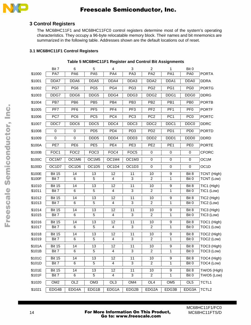
3 Control RegistersThe MC68HC11F1 and MC68HC11FC0 control registers determine most of the system’s operatingcharacteristics. They occupy a 96-byte relocatable memory block. Their names and bit mnemonics aresummarized in the following table. Addresses shown are the default locations out of reset.
3.1 MC68HC11F1 Control Registers
Table 5 MC68HC11F1 Register and Control Bit Assignments
Bit 7 6 5 4 3 2 1 Bit 0$1000 PA7 PA6 PA5 PA4 PA3 PA2 PA1 PA0 PORTA
$1001 DDA7 DDA6 DDA5 DDA4 DDA3 DDA2 DDA1 DDA0 DDRA
$1002 PG7 PG6 PG5 PG4 PG3 PG2 PG1 PG0 PORTG
$1003 DDG7 DDG6 DDG5 DDG4 DDG3 DDG2 DDG1 DDG0 DDRG
$1004 PB7 PB6 PB5 PB4 PB3 PB2 PB1 PB0 PORTB
$1005 PF7 PF6 PF5 PF4 PF3 PF2 PF1 PF0 PORTF
$1006 PC7 PC6 PC5 PC4 PC3 PC2 PC1 PC0 PORTC
$1007 DDC7 DDC6 DDC5 DDC4 DDC3 DDC2 DDC1 DDC0 DDRC
$1008 0 0 PD5 PD4 PD3 PD2 PD1 PD0 PORTD
$1009 0 0 DDD5 DDD4 DDD3 DDD2 DDD1 DDD0 DDRD
$100A PE7 PE6 PE5 PE4 PE3 PE2 PE1 PE0 PORTE
$100B FOC1 FOC2 FOC3 FOC4 FOC5 0 0 0 CFORC
$100C OC1M7 OC1M6 OC1M5 OC1M4 OC1M3 0 0 0 OC1M
$100D OC1D7 OC1D6 OC1D5 OC1D4 OC1D3 0 0 0 OC1D
$100E Bit 15 14 13 12 11 10 9 Bit 8 TCNT (High)$100F Bit 7 6 5 4 3 2 1 Bit 0 TCNT (Low)
$1010 Bit 15 14 13 12 11 10 9 Bit 8 TIC1 (High)$1011 Bit 7 6 5 4 3 2 1 Bit 0 TIC1 (Low)
$1012 Bit 15 14 13 12 11 10 9 Bit 8 TIC2 (High)$1013 Bit 7 6 5 4 3 2 1 Bit 0 TIC2 (Low)
$1014 Bit 15 14 13 12 11 10 9 Bit 8 TIC3 (High)$1015 Bit 7 6 5 4 3 2 1 Bit 0 TIC3 (Low)
$1016 Bit 15 14 13 12 11 10 9 Bit 8 TOC1 (High)$1017 Bit 7 6 5 4 3 2 1 Bit 0 TOC1 (Low)
$1018 Bit 15 14 13 12 11 10 9 Bit 8 TOC2 (High)$1019 Bit 7 6 5 4 3 2 1 Bit 0 TOC2 (Low)
$101A Bit 15 14 13 12 11 10 9 Bit 8 TOC3 (High)$101B Bit 7 6 5 4 3 2 1 Bit 0 TOC3 (Low)
$101C Bit 15 14 13 12 11 10 9 Bit 8 TOC4 (High)$101D Bit 7 6 5 4 3 2 1 Bit 0 TOC4 (Low)
$101E Bit 15 14 13 12 11 10 9 Bit 8 TI4/O5 (High)$101F Bit 7 6 5 4 3 2 1 Bit 0 TI4/O5 (Low)
$1020 OM2 OL2 OM3 OL3 OM4 OL4 OM5 OL5 TCTL1
$1021 EDG4B EDG4A EDG1B EDG1A EDG2B EDG2A EDG3B EDG3A TCTL2
MC68HC11F1/FC014 MC68HC11FTS/D
For More Information On This Product,
Go to: www.freescale.com

F
ree
sca
le S
em
ico
nd
uc
tor,
I
Freescale Semiconductor, Inc.n
c..
.
$1022 OC1I OC2I OC3I OC4I I4/O5I IC1I IC2I IC3I TMSK1$1023 OC1F OC2F OC3F OC4F I4/O5F IC1F IC2F IC3F TFLG1
$1024 TOI RTII PAOVI PAII 0 0 PR1 PR0 TMSK2
$1025 TOF RTIF PAOVF PAIF 0 0 0 0 TFLG2
$1026 0 PAEN PAMOD PEDGE 0 I4/05 RTR1 RTR0 PACTL
$1027 Bit 7 6 5 4 3 2 1 Bit 0 PACNT
$1028 SPIE SPE DWOM MSTR CPOL CPHA SPR1 SPR0 SPCR
$1029 SPIF WCOL 0 MODF 0 0 0 0 SPSR
$102A Bit 7 6 5 4 3 2 1 Bit 0 SPDR
$102B TCLR SCP2 SCP1 SCP0 RCKB SCR2 SCR1 SCR0 BAUD
$102C R8 T8 0 M WAKE 0 0 0 SCCR1
$102D TIE TCIE RIE ILIE TE RE RWU SBK SCCR2
$102E TDRE TC RDRF IDLE OR NF FE 0 SCSR
$102F Bit 7 6 5 4 3 2 1 Bit 0 SCDR
$1030 CCF 0 SCAN MULT CD CC CB CA ADCTL
$1031 Bit 7 6 5 4 3 2 1 Bit 0 ADR1
$1032 Bit 7 6 5 4 3 2 1 Bit 0 ADR2
$1033 Bit 7 6 5 4 3 2 1 Bit 0 ADR3
$1034 Bit 7 6 5 4 3 2 1 Bit 0 ADR4
$1035 0 0 0 PTCON BPRT3 BPRT2 BPRT1 BPRT0 BPROT
$1036 Reserved
$1037 Reserved
$1038 GWOM CWOM CLK4X LIRDV 0 SPRBYP 0 0 OPT2
$1039 0 0 IRQE DLY CME FCME CR1 CR0 OPTION
$103A Bit 7 6 5 4 3 2 1 Bit 0 COPRST
$103B ODD EVEN 0 BYTE ROW ERASE EELAT EEPGM PPROG
$103C RBOOT SMOD MDA IRV PSEL3 PSEL2 PSEL1 PSEL0 HPRIO
$103D RAM3 RAM2 RAM1 RAM0 REG3 REG2 REG1 REG0 INIT
$103E TILOP 0 OCCR CBYP DISR FCM FCOP 0 TEST1
$103F EE3 EE2 EE1 EE0 1 NOCOP 1 EEON CONFIG
$1040 Reservedto
$105B Reserved
$105C I01SA I01SB I02SA I02SB GSTHA GSTGB PSTHA PSTHB CSSTRH
$105D I01EN I01PL I02EN I02PL GCSPR PCSEN PSIZA PSIZB CSCTL
$105E GA15 GA14 GA13 GA12 GA11 GA10 0 0 CSGADR
$105F I01AV I02AV 0 GNPOL GAVLD GSIZA GSIZB GSIZC CSGSIZ
Table 5 MC68HC11F1 Register and Control Bit Assignments (Continued)
Bit 7 6 5 4 3 2 1 Bit 0
MC68HC11F1/FC0 MC68HC11FTS/D 15
For More Information On This Product,
Go to: www.freescale.com

F
ree
sca
le S
em
ico
nd
uc
tor,
I
Freescale Semiconductor, Inc.n
c..
.
3.2 MC68HC11FC0 Control Registers
Table 6 MC68HC11FC0 Register and Control Bit Assignments
Bit 7 6 5 4 3 2 1 Bit 0$1000 PA7 PA6 PA5 PA4 PA3 PA2 PA1 PA0 PORTA
$1001 DDA7 DDA6 DDA5 DDA4 DDA3 DDA2 DDA1 DDA0 DDRA
$1002 PG7 PG6 PG5 PG4 PG3 PG2 PG1 PG0 PORTG
$1003 DDG7 DDG6 DDG5 DDG4 DDG3 DDG2 DDG1 DDG0 DDRG
$1004 PB7 PB6 PB5 PB4 PB3 PB2 PB1 PB0 PORTB
$1005 PF7 PF6 PF5 PF4 PF3 PF2 PF1 PF0 PORTF
$1006 PC7 PC6 PC5 PC4 PC3 PC2 PC1 PC0 PORTC
$1007 DDC7 DDC6 DDC5 DDC4 DDC3 DDC2 DDC1 DDC0 DDRC
$1008 0 0 PD5 PD4 PD3 PD2 PD1 PD0 PORTD
$1009 0 0 DDD5 DDD4 DDD3 DDD2 DDD1 DDD0 DDRD
$100A PE7 PE6 PE5 PE4 PE3 PE2 PE1 PE0 PORTE
$100B FOC1 FOC2 FOC3 FOC4 FOC5 0 0 0 CFORC
$100C OC1M7 OC1M6 OC1M5 OC1M4 OC1M3 0 0 0 OC1M
$100D OC1D7 OC1D6 OC1D5 OC1D4 OC1D3 0 0 0 OC1D
$100E Bit 15 14 13 12 11 10 9 Bit 8 TCNT (High)$100F Bit 7 6 5 4 3 2 1 Bit 0 TCNT (Low)
$1010 Bit 15 14 13 12 11 10 9 Bit 8 TIC1 (High)$1011 Bit 7 6 5 4 3 2 1 Bit 0 TIC1 (Low)
$1012 Bit 15 14 13 12 11 10 9 Bit 8 TIC2 (High)$1013 Bit 7 6 5 4 3 2 1 Bit 0 TIC2 (Low)
$1014 Bit 15 14 13 12 11 10 9 Bit 8 TIC3 (High)$1015 Bit 7 6 5 4 3 2 1 Bit 0 TIC3 (Low)
$1016 Bit 15 14 13 12 11 10 9 Bit 8 TOC1 (High)$1017 Bit 7 6 5 4 3 2 1 Bit 0 TOC1 (Low)
$1018 Bit 15 14 13 12 11 10 9 Bit 8 TOC2 (High)$1019 Bit 7 6 5 4 3 2 1 Bit 0 TOC2 (Low)
$101A Bit 15 14 13 12 11 10 9 Bit 8 TOC3 (High)$101B Bit 7 6 5 4 3 2 1 Bit 0 TOC3 (Low)
$101C Bit 15 14 13 12 11 10 9 Bit 8 TOC4 (High)$101D Bit 7 6 5 4 3 2 1 Bit 0 TOC4 (Low)
$101E Bit 15 14 13 12 11 10 9 Bit 8 TI4/O5 (High)$101F Bit 7 6 5 4 3 2 1 Bit 0 TI4/O5 (Low)
$1020 OM2 OL2 OM3 OL3 OM4 OL4 OM5 OL5 TCTL1
$1021 EDG4B EDG4A EDG1B EDG1A EDG2B EDG2A EDG3B EDG3A TCTL2
$1022 OC1I OC2I OC3I OC4I I4/O5I IC1I IC2I IC3I TMSK1$1023 OC1F OC2F OC3F OC4F I4/O5F IC1F IC2F IC3F TFLG1
$1024 TOI RTII PAOVI PAII 0 0 PR1 PR0 TMSK2
$1025 TOF RTIF PAOVF PAIF 0 0 0 0 TFLG2
MC68HC11F1/FC016 MC68HC11FTS/D
For More Information On This Product,
Go to: www.freescale.com

F
ree
sca
le S
em
ico
nd
uc
tor,
I
Freescale Semiconductor, Inc.n
c..
.
$1026 0 PAEN PAMOD PEDGE 0 I4/05 RTR1 RTR0 PACTL
$1027 Bit 7 6 5 4 3 2 1 Bit 0 PACNT
$1028 SPIE SPE DWOM MSTR CPOL CPHA SPR1 SPR0 SPCR
$1029 SPIF WCOL 0 MODF 0 0 0 0 SPSR
$102A Bit 7 6 5 4 3 2 1 Bit 0 SPDR
$102B TCLR SCP2 SCP1 SCP0 RCKB SCR2 SCR1 SCR0 BAUD
$102C R8 T8 0 M WAKE 0 0 0 SCCR1
$102D TIE TCIE RIE ILIE TE RE RWU SBK SCCR2
$102E TDRE TC RDRF IDLE OR NF FE 0 SCSR
$102F Bit 7 6 5 4 3 2 1 Bit 0 SCDR
$1030 Reservedto
$1037 Reserved
$1038 GWOM CWOM CLK4X LIRDV 0 SPRBYP 0 0 OPT2
$1039 0 0 IRQE DLY CME FCME CR1 CR0 OPTION
$103A Bit 7 6 5 4 3 2 1 Bit 0 COPRST
$103B Reserved
$103C RBOOT SMOD MDA IRV PSEL3 PSEL2 PSEL1 PSEL0 HPRIO
$103D RAM5 RAM4 RAM3 RAM2 RAM1 RAM0 REG1 REG0 INIT
$103E TILOP 0 OCCR CBYP DISR FCM FCOP 0 TEST1
$103F 0 0 0 0 0 NOCOP 0 0 CONFIG
$1040 Reservedto
$105B Reserved
$105C I01SA I01SB I02SA I02SB GSTHA GSTGB PSTHA PSTHB CSSTRH
$105D I01EN I01PL I02EN I02PL GCSPR PCSEN PSIZA PSIZB CSCTL
$105E GA15 GA14 GA13 GA12 GA11 GA10 0 0 CSGADR
$105F I01AV I02AV 0 GNPOL GAVLD GSIZA GSIZB GSIZC CSGSIZ
Table 6 MC68HC11FC0 Register and Control Bit Assignments (Continued)
Bit 7 6 5 4 3 2 1 Bit 0
MC68HC11F1/FC0 MC68HC11FTS/D 17
For More Information On This Product,
Go to: www.freescale.com

F
ree
sca
le S
em
ico
nd
uc
tor,
I
Freescale Semiconductor, Inc.n
c..
.
4 Operating Modes and System InitializationThe 16-bit address bus can access 64 Kbytes of memory. Because the MC68HC11F1 andMC68HC11FC0 are intended to operate principally in expanded mode, there is no internal ROM andthe address bus is non-multiplexed. Both devices include 1 Kbyte of static RAM, a 96-byte control reg-ister block, and 256 bytes of bootstrap ROM. The MC68HC11F1 also includes 512 bytes of EEPROM.
RAM and registers can be remapped on both the MC68HC11F1 and the MC68HC11FC0. On both theMC68HC11F1 and the MC68HC11FC0, out of reset RAM resides at $0000 to $03FF and registers re-side at $1000 to $105F. On the MC68HC11F1, RAM and registers can both be remapped to any 4-Kbyte boundary. On the MC68HC11FC0, RAM can be remapped to any 1-Kbyte boundary, and regis-ters can be remapped to any 4-Kbyte boundary in the first 16 Kbytes of address space.
RAM and control register locations are defined by the INIT register, which can be written only once with-in the first 64 E-clock cycles after a reset in normal modes. It becomes a read-only register thereafter.If RAM and the control register block are mapped to the same boundary, the register block has priorityof the first 96 bytes.
In expanded and special test modes in the MC68HC11F1, EEPROM is located from $xE00 to $xFFF,where x represents the value of the four high-order bits of the CONFIG register. EEPROM is enabledby the EEON bit of the CONFIG register. In single-chip and bootstrap modes, the EEPROM is locatedfrom $FE00 to $FFFF.
4.1 Operating Modes
Bootstrap ROM resides at addresses $BF00–$BFFF, and is only available when the MCU operates inspecial bootstrap operating mode. Operating modes are determined by the logic levels applied to theMODB and MODA pins at reset.
In single-chip mode, the MCU functions as a self-contained microcontroller and has no external addressor data bus. Ports B, C and F are available for general-purpose I/O (GPIO). Ports B and F are outputsonly; each of the port C pins can be configured as input or output.
CAUTIONThe MC68HC11FC0 must not be configured to boot in single-chip mode becauseit has no internal ROM or EEPROM. Operation of the device in single-chip modewill result in erratic behavior.
In expanded mode, the MCU can access external memory. Ports B and F provide the address bus, andport C is the data bus.
Special bootstrap mode is a variation of single chip mode that provides access to the internal bootstrapROM. In this mode, the user can download a program into on-chip RAM through the serial communica-tion interface (SCI).
Special test mode, a variation of expanded mode, is primarily used during Motorola’s internal productiontesting, but can support emulation and debugging during program development.
Table 7 shows a summary of operating modes, mode select pins, and control bits in the HPRIO register.
Table 7 Hardware Mode Select Summary
Input PinsMode Description
Control Bits in HPRIO (Latched at Reset)MODB MODA RBOOT SMOD MDA
1 0 Single Chip 0 0 01 1 Expanded 0 0 10 0 Special Bootstrap 1 1 00 1 Special Test 0 1 1
MC68HC11F1/FC018 MC68HC11FTS/D
For More Information On This Product,
Go to: www.freescale.com

F
ree
sca
le S
em
ico
nd
uc
tor,
I
Freescale Semiconductor, Inc.n
c..
.
4.2 Memory Maps
NOTES:1. RAM can be remapped to any 4-Kbyte boundary ($x000). “x” represents the value contained in RAM[3:0] in the
INIT register.2. The register block can be remapped to any 4-Kbyte boundary ($y000). “y” represents the value contained in
REG[3:0] in the INIT register.3. Special test mode vectors are externally addressed.4. In special test mode the address locations $zD00—$zDFF are not externally addressable. “z” represents the val-
ue of bits EE[3:0] in the CONFIG register.5. EEPROM can be remapped to any 4-Kbyte boundary ($z000). “z” represents the value contained in EE[3:0] in
the CONFIG register.
Figure 7 MC68HC11F1 Memory Map
$0000 —
$03FF —
$1000 —
$105F —
$FFC0 —
$FFFF —SINGLE
CHIP
MODA = 0MODB = 1
—
EXPANDED
MODA = 1MODB = 1
—
—
—
—
—
—
—
—
—
—
—
—
—
—
—
—
SPECIALTEST
MODA = 1MODB = 0
—
—
—
—
—
—
—SPECIAL
BOOTSTRAP
MODA = 0MODB = 0
$BF00 —
$BFFF —
EXTERNAL
EXTERNAL
EXTERNAL
EXTERNAL
SPECIALMODE
VECTORS3
$BFC0
$BFFF
NORMALMODE
VECTORS$FFFF
$FE00 — 512
BYTESEEPROM5
RESERVED4
INTERRUPT
INTERRUPT
1024 BYTES RAM1
x000
x3FF
96-BYTE REGISTER FILE2
y000
y05F
$FFC0
256 BYTESBOOTSTRAP
ROM
MC68HC11F1/FC0 MC68HC11FTS/D 19
For More Information On This Product,
Go to: www.freescale.com

F
ree
sca
le S
em
ico
nd
uc
tor,
I
Freescale Semiconductor, Inc.n
c..
.
NOTES:1. RAM can be remapped to any 1-Kbyte boundary, depending on the value contained in the RAM field in the INIT
register.2. The register block can be remapped to $0000, $2000, or $3000, depending on the value contained in REG[1:0]
in the INIT register.
Figure 8 MC68HC11FC0 Memory Map
4.3 System Initialization Registers
HPRIO — Highest Priority Interrupt and Miscellaneous $x03C
Bit 7 6 5 4 3 2 1 Bit 0
RBOOT SMOD MDA IRV PSEL3 PSEL2 PSEL1 PSEL0
RESET: 0 0 0 0 0 1 0 1 Single-Chip
0 0 1 0 0 1 0 1 Expanded
1 1 0 1 0 1 0 1 Bootstrap
0 1 1 1 0 1 0 1 Special Test
$0000 —
$03FF —
$1000 —
$105F —
$FFC0 —
$FFFF —SINGLE
CHIP
MODA = 0MODB = 1
—
EXPANDED
MODA = 1MODB = 1
—
—
—
—
—
—
—
—
—
—
—
—
—
—
—
—
SPECIALTEST
MODA = 1MODB = 0
—
—
—
—
—
—
—SPECIAL
BOOTSTRAP
MODA = 0MODB = 0
$BF00 —
$BFFF —
EXTERNAL
EXTERNAL
EXTERNAL
EXTERNAL
SPECIALMODE
VECTORS
$BFC0
$BFFF
NORMALMODE
VECTORS$FFFF
$FE00 —
INTERRUPT
INTERRUPT
1024 BYTES RAM1
96-BYTE REGISTER FILE2
$FFC0
256 BYTESBOOTSTRAP
ROM
MC68HC11F1/FC020 MC68HC11FTS/D
For More Information On This Product,
Go to: www.freescale.com
F
ree
sca
le S
em
ico
nd
uc
tor,
I
Freescale Semiconductor, Inc.n
c..
.
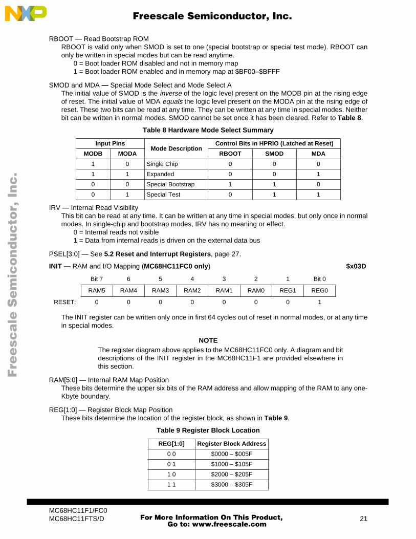
RBOOT — Read Bootstrap ROMRBOOT is valid only when SMOD is set to one (special bootstrap or special test mode). RBOOT canonly be written in special modes but can be read anytime.
0 = Boot loader ROM disabled and not in memory map1 = Boot loader ROM enabled and in memory map at $BF00–$BFFF
SMOD and MDA — Special Mode Select and Mode Select AThe initial value of SMOD is the inverse of the logic level present on the MODB pin at the rising edgeof reset. The initial value of MDA equals the logic level present on the MODA pin at the rising edge ofreset. These two bits can be read at any time. They can be written at any time in special modes. Neitherbit can be written in normal modes. SMOD cannot be set once it has been cleared. Refer to Table 8.
IRV — Internal Read VisibilityThis bit can be read at any time. It can be written at any time in special modes, but only once in normalmodes. In single-chip and bootstrap modes, IRV has no meaning or effect.
0 = Internal reads not visible1 = Data from internal reads is driven on the external data bus
PSEL[3:0] — See 5.2 Reset and Interrupt Registers, page 27.
The INIT register can be written only once in first 64 cycles out of reset in normal modes, or at any timein special modes.
NOTEThe register diagram above applies to the MC68HC11FC0 only. A diagram and bitdescriptions of the INIT register in the MC68HC11F1 are provided elsewhere inthis section.
RAM[5:0] — Internal RAM Map PositionThese bits determine the upper six bits of the RAM address and allow mapping of the RAM to any one-Kbyte boundary.
REG[1:0] — Register Block Map PositionThese bits determine the location of the register block, as shown in Table 9.
Table 8 Hardware Mode Select Summary
Input PinsMode Description
Control Bits in HPRIO (Latched at Reset)
MODB MODA RBOOT SMOD MDA
1 0 Single Chip 0 0 0
1 1 Expanded 0 0 1
0 0 Special Bootstrap 1 1 0
0 1 Special Test 0 1 1
INIT — RAM and I/O Mapping (MC68HC11FC0 only) $x03D
Bit 7 6 5 4 3 2 1 Bit 0
RAM5 RAM4 RAM3 RAM2 RAM1 RAM0 REG1 REG0
RESET: 0 0 0 0 0 0 0 1
Table 9 Register Block Location
REG[1:0] Register Block Address
0 0 $0000 – $005F
0 1 $1000 – $105F
1 0 $2000 – $205F
1 1 $3000 – $305F
MC68HC11F1/FC0 MC68HC11FTS/D 21
For More Information On This Product,
Go to: www.freescale.com

F
ree
sca
le S
em
ico
nd
uc
tor,
I
Freescale Semiconductor, Inc.n
c..
.
The INIT register can be written only once in first 64 cycles out of reset in normal modes, or at any timein special modes.
NOTEThe register diagram above applies to the MC68HC11F1 only. A diagram and bitdescriptions of the INIT register in the MC68HC11FC0 are provided elsewhere inthis section.
RAM[3:0] — Internal RAM Map PositionThese bits determine the upper four bits of the RAM address and allow mapping of the RAM to any four-Kbyte boundary. Refer to Table 10.
REG[3:0] — 96-Byte Register Block Map PositionThese bits determine bits the upper 4 bits of the register block and allow mapping of the register blockto any four-Kbyte boundary. Refer to Table 10.
GWOM — Port G Wired-OR Mode OptionRefer to 7.8 Parallel I/O Registers, page 36.
INIT — RAM and I/O Mapping (MC68HC11F1 only) $x03D
Bit 7 6 5 4 3 2 1 Bit 0
RAM3 RAM2 RAM1 RAM0 REG3 REG4 REG1 REG0
RESET: 0 0 0 0 0 0 0 1
Table 10 RAM and Register Mapping
RAM[3:0] Location REG[3:0] Location
0000 $0000-$03FF 0000 $0000-$005F
0001 $1000-$13FF 0001 $1000-$105F
0010 $2000-$23FF 0010 $2000-$205F
0011 $3000-$33FF 0011 $3000-$305F
0100 $4000-$43FF 0100 $4000-$405F
0101 $5000-$53FF 0101 $5000-$505F
0110 $6000-$63FF 0110 $6000-$605F
0111 $7000-$73FF 0111 $7000-$705F
1000 $8000-$83FF 1000 $8000-$805F
1001 $9000-$93FF 1001 $9000-$905F
1010 $A000-$A3FF 1010 $A000-$A05F
1011 $B000-$B3FF 1011 $B000-$B05F
1100 $C000-$C3FF 1100 $C000-$C05F
1101 $D000-$D3FF 1101 $D000-$D05F
1110 $E000-$E3FF 1110 $E000-$E05F
1111 $F000-$F3FF 1111 $F000-$F05F
OPT2 — System Configuration Option Register 2 $x038
Bit 7 6 5 4 3 2 1 Bit 0
GWOM CWOM CLK4X LIRDV — SPRBYP — —
RESET 0 0 1 0 0 0 0 0
MC68HC11F1/FC022 MC68HC11FTS/D
For More Information On This Product,
Go to: www.freescale.com

F
ree
sca
le S
em
ico
nd
uc
tor,
I
Freescale Semiconductor, Inc.n
c..
.
CWOM — Port C Wired-OR Mode OptionRefer to 7.8 Parallel I/O Registers, page 37.
CLK4X — 4XCLK Output EnableThis bit can only be written once after reset in all modes.
0 = 4XOUT clock output is disabled1 = Buffered oscillator is driven on the 4XOUT clock output
LIRDV — Load Instruction Register DrivenIn order to detect consecutive instructions in a high-speed application, LIR can be driven high for onequarter of an E-clock cycle during each instruction fetch.
0 = LIR signal is not driven high.1 = LIR signal is driven high.
Bits 3, 1, 0 — Not implemented. Reads always return zero and writes have no effect.
SPRBYP — See 10.2 SPI Registers, page 52.
*Can be written only once in first 64 cycles out of reset in normal modes, or at any time in special modes.
ADPU — A/D Power-UpThis bit is implemented on the MC68HC11F1 only. On the MC68HC11FC0, reads always return zeroand writes have no effect.
0 = A/D system disabled1 = A/D system enabled
CSEL — Clock SelectThis bit is implemented on the MC68HC11F1 only. On the MC68HC11FC0, reads always return zeroand writes have no effect.
0 = A/D and EEPROM use system E clock1 = A/D and EEPROM use internal RC clock
IRQE — IRQ Select Edge Sensitive Only0 = Low level recognition1 = Falling edge recognition
DLY — Enable Oscillator Start-Up Delay on Exit from STOP0 = No stabilization delay on exit from STOP1 = Stabilization delay of 4064 E-clock cycles is enabled on exit from STOP
CME — Clock Monitor Enable0 = Clock monitor disabled; slow clocks can be used1 = Slow or stopped clocks cause clock failure reset
FCME — Force Clock Monitor Enable0 = Clock monitor circuit follows the state of the CME bit1 = Clock monitor circuit is enabled until the next reset
In order to use both STOP and the clock monitor, the CME bit should be written to zero prior to executinga STOP instruction and rewritten to one after recovery from STOP. FCME should be kept cleared if theuser intends to use the STOP instruction.
CR[1:0] — COP Timer Rate SelectRefer to 5.2 Reset and Interrupt Registers, page 27.
OPTION — System Configuration Options $x039
Bit 7 6 5 4 3 2 1 Bit 0
ADPU CSEL IRQE* DLY* CME FCME* CR1* CR0*
RESET: 0 0 0 1 0 0 0 0
MC68HC11F1/FC0 MC68HC11FTS/D 23
For More Information On This Product,
Go to: www.freescale.com
F
ree
sca
le S
em
ico
nd
uc
tor,
I
Freescale Semiconductor, Inc.n
c..
.
U = Unaffected by reset
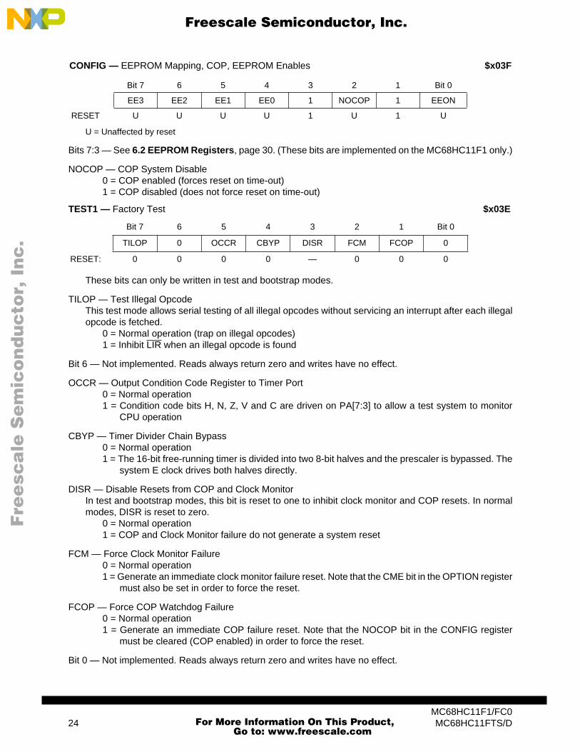
Bits 7:3 — See 6.2 EEPROM Registers, page 30. (These bits are implemented on the MC68HC11F1 only.)
NOCOP — COP System Disable0 = COP enabled (forces reset on time-out)1 = COP disabled (does not force reset on time-out)
These bits can only be written in test and bootstrap modes.
TILOP — Test Illegal OpcodeThis test mode allows serial testing of all illegal opcodes without servicing an interrupt after each illegalopcode is fetched.
0 = Normal operation (trap on illegal opcodes)1 = Inhibit LIR when an illegal opcode is found
Bit 6 — Not implemented. Reads always return zero and writes have no effect.
OCCR — Output Condition Code Register to Timer Port0 = Normal operation1 = Condition code bits H, N, Z, V and C are driven on PA[7:3] to allow a test system to monitor
CPU operation
CBYP — Timer Divider Chain Bypass0 = Normal operation1 = The 16-bit free-running timer is divided into two 8-bit halves and the prescaler is bypassed. The
system E clock drives both halves directly.
DISR — Disable Resets from COP and Clock MonitorIn test and bootstrap modes, this bit is reset to one to inhibit clock monitor and COP resets. In normalmodes, DISR is reset to zero.
0 = Normal operation1 = COP and Clock Monitor failure do not generate a system reset
FCM — Force Clock Monitor Failure0 = Normal operation1 = Generate an immediate clock monitor failure reset. Note that the CME bit in the OPTION register
must also be set in order to force the reset.
FCOP — Force COP Watchdog Failure0 = Normal operation1 = Generate an immediate COP failure reset. Note that the NOCOP bit in the CONFIG register
must be cleared (COP enabled) in order to force the reset.
Bit 0 — Not implemented. Reads always return zero and writes have no effect.
CONFIG — EEPROM Mapping, COP, EEPROM Enables $x03F
Bit 7 6 5 4 3 2 1 Bit 0
EE3 EE2 EE1 EE0 1 NOCOP 1 EEON
RESET U U U U 1 U 1 U
TEST1 — Factory Test $x03E
Bit 7 6 5 4 3 2 1 Bit 0
TILOP 0 OCCR CBYP DISR FCM FCOP 0
RESET: 0 0 0 0 — 0 0 0
MC68HC11F1/FC024 MC68HC11FTS/D
For More Information On This Product,
Go to: www.freescale.com

F
ree
sca
le S
em
ico
nd
uc
tor,
I
Freescale Semiconductor, Inc.n
c..
.
5 Resets and InterruptsThere are three sources of reset on the MC68HC11F1 and MC68HC11FC0, each having its own resetvector:
• RESET pin• Clock monitor failure• Computer operating properly (COP) failure
There are 22 interrupt sources serviced by 18 interrupt vectors. (The SCI interrupt vector services fiveSCI interrupt sources.) Three of the interrupt vectors are non-maskable:
• Illegal opcode trap• Software interrupt• XIRQ pin (pseudo non-maskable interrupt)
The other 19 interrupts, generated mostly by on-chip peripheral systems, are maskable. Maskable in-terrupts are recognized only if the global interrupt mask bit (I) in the condition code register (CCR) isclear. Maskable interrupts have a default priority arrangement out of reset. However, any one interruptsource can be elevated to the highest maskable priority position by writing to the HPRIO register. Thisregister can be written at any time, provided the I bit in the CCR is set.
In addition to the global I bit, all maskable interrupt sources except the external interrupt (IRQ pin) aresubject to local enable bits in control registers. Each of these interrupt sources also sets a correspond-ing flag bit in a control register that can be polled by software.
Several of these flags are automatically cleared during the normal course of responding to the interruptrequests. For example, the RDRF flag is set when a byte has been received in the SCI. The normalresponse to an RDRF interrupt request is to read the SCI status register to check for receive errors,then to read the received data from the SCI data register. It is precisely these two steps that are requiredto clear the RDRF flag, so no further instructions are necessary.
5.1 Interrupt Sources
The following table summarizes the interrupt sources, vector addresses, masks, and flag bits.
MC68HC11F1/FC0 MC68HC11FTS/D 25
For More Information On This Product,
Go to: www.freescale.com

F
ree
sca
le S
em
ico
nd
uc
tor,
I
Freescale Semiconductor, Inc.n
c..
.
5.2 Reset and Interrupt Registers
*Can be written only once in first 64 cycles out of reset in normal modes, or at any time in special modes.
Bits [7:6], [4:2]Refer to 4.3 System Initialization Registers, page 23, and 11.3 A/D Registers, page 56.
IRQE — IRQ Select Edge Sensitive Only0 = Low level recognition1 = Falling edge recognition
Table 11 Interrupt and Reset Vector Assignments
Vector Address Interrupt Source CCR Mask Local Mask Flag Bit
FFC0, C1to
FFD4, D5Reserved — — —
FFD6, D7 SCI Serial System
I Bit
SCI Transmit Complete TCIE TC
SCI Transmit Data Register Empty TIE TDRE
SCI Idle Line Detect ILIE IDLE
SCI Receiver Overrun RIE OR
SCI Receive Data Register Full RIE RDRF
FFD8, D9 SPI Serial Transfer Complete I Bit SPIE SPIF
FFDA, DB Pulse Accumulator Input Edge I Bit PAII PAIF
FFDC, DD Pulse Accumulator Overflow I Bit PAOVI PAOVF
FFDE, DF Timer Overflow I Bit TOI TOF
FFE0, E1 Timer Input Capture 4/Output Compare 5 I Bit I4/O5I I4/O5F
FFE2, E3 Timer Output Compare 4 I Bit OC4I OC4F
FFE4, E5 Timer Output Compare 3 I Bit OC3I OC3F
FFE6, E7 Timer Output Compare 2 I Bit OC2I OC2F
FFE8, E9 Timer Output Compare 1 I Bit OC1I OC1F
FFEA, EB Timer Input Capture 3 I Bit IC3I IC3F
FFEC, ED Timer Input Capture 2 I Bit IC2I IC2F
FFEE, EF Timer Input Capture 1 I Bit IC1I IC1F
FFF0, F1 Real-Time Interrupt I Bit RTII RTIF
FFF2, F3 IRQ I Bit None None
FFF4, F5 XIRQ Pin X Bit None None
FFF6, F7 Software Interrupt None None None
FFF8, F9 Illegal Opcode Trap None None None
FFFA, FB COP Failure None NOCOP None
FFFC, FD Clock Monitor Fail None CME None
FFFE, FF RESET None None None
OPTION — System Configuration Options $x039
Bit 7 6 5 4 3 2 1 Bit 0
ADPU CSEL IRQE* DLY* CME FCME* CR1* CR0*
RESET: 0 0 0 1 0 0 0 0
MC68HC11F1/FC026 MC68HC11FTS/D
For More Information On This Product,
Go to: www.freescale.com

F
ree
sca
le S
em
ico
nd
uc
tor,
I
Freescale Semiconductor, Inc.n
c..
.
CR[1:0] — COP Timer Rate Select
The COP system is driven by a constant frequency of E/215. CR[1:0] specify an additional divide-by fac-tor to arrive at the COP time-out rate.
Write $55 to COPRST to arm the COP watchdog clearing mechanism. Then write $AA to COPRST toreset the COP timer. Performing instructions between these two steps is possible provided both stepsare completed in the correct sequence before the timer times out.
Bits [7:4] — See 4.3 System Initialization Registers, page 20.
PSEL[3:0] — Interrupt Priority Select BitsCan be written only while the I bit in the CCR is set (interrupts disabled). These bits select one interruptsource to have priority over other I-bit related sources.
Table 12 COP Watchdog Time-Out Periods
Frequency Tolerance CR[1:0] = 00 CR[1:0] = 01 CR[1:0] = 10 CR[1:0] = 11
1 MHz -0/+32.768 ms 32.768 ms 131.072 ms 524.288 ms 2.097 s
2 MHz -0/+16.384 ms 16.384 ms 65.536 ms 262.144 ms 1.049 s
3 MHz -0/+10.923 ms 10.923 ms 43.691 ms 174.763 ms 699.051 ms
4 MHz -0/+8.192 ms 8.192 ms 32.768 ms 131.072 ms 524.288 ms
5 MHz -0/+6.554 ms 6.554 ms 26.214 ms 104.858 ms 419.430 ms
6 MHz -0/+5.461 ms 5.461 ms 21.845 87.381 ms 349.525 ms
Any E -0/+215/E 215/E 217/E 219/E 221/E
COPRST — Arm/Reset COP Timer Circuitry $x03A
Bit 7 6 5 4 3 2 1 Bit 0
7 6 5 4 3 2 1 0
RESET: 0 0 0 0 0 0 0 0
HPRIO — Highest Priority I-Bit Interrupt and Miscellaneous $x03C
Bit 7 6 5 4 3 2 1 Bit 0
RBOOT SMOD MDA IRV PSEL3 PSEL2 PSEL1 PSEL0
RESET: 0 1 0 1
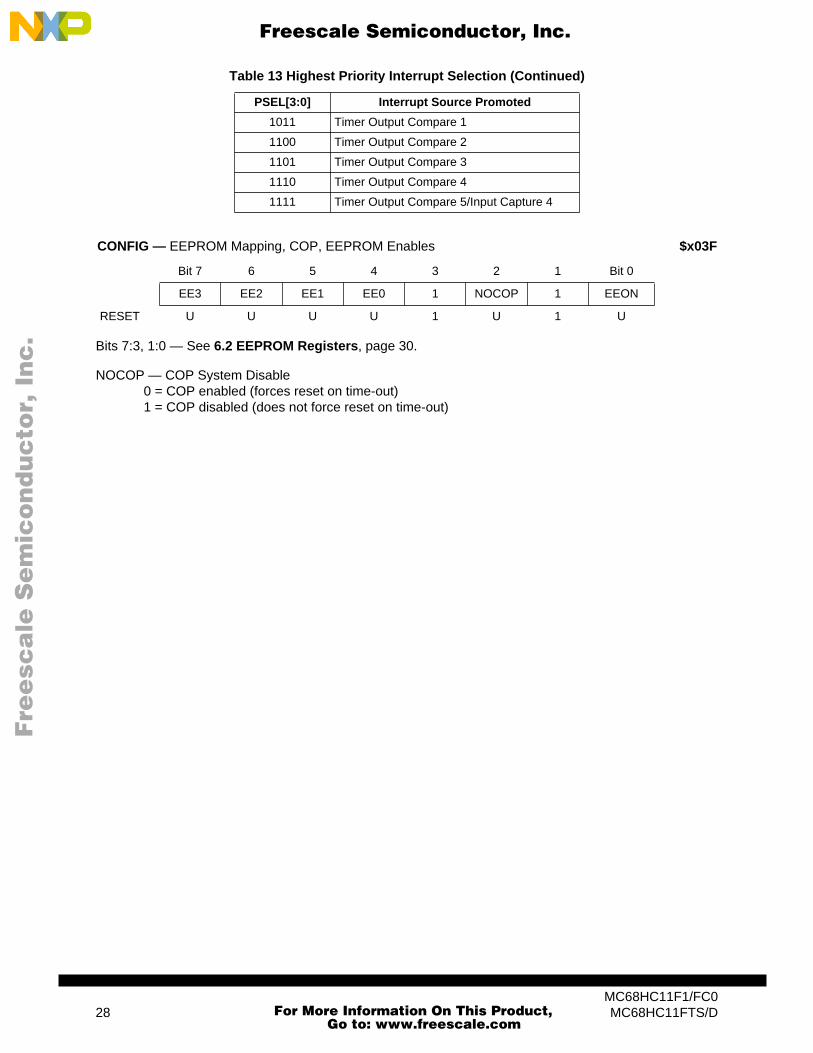
Table 13 Highest Priority Interrupt Selection
PSEL[3:0] Interrupt Source Promoted
0000 Timer Overflow
0001 Pulse Accumulator Overflow
0010 Pulse Accumulator Input Edge
0011 SPI Serial Transfer Complete
0100 SCI Serial System
0101 Reserved (Default to IRQ)
0110 IRQ (External Pin)
0111 Real-Time Interrupt
1000 Timer Input Capture 1
1001 Timer Input Capture 2
1010 Timer Input Capture 3
MC68HC11F1/FC0 MC68HC11FTS/D 27
For More Information On This Product,
Go to: www.freescale.com
F
ree
sca
le S
em
ico
nd
uc
tor,
I
Freescale Semiconductor, Inc.n
c..
.
Bits 7:3, 1:0 — See 6.2 EEPROM Registers, page 30.
NOCOP — COP System Disable0 = COP enabled (forces reset on time-out)1 = COP disabled (does not force reset on time-out)
1011 Timer Output Compare 1
1100 Timer Output Compare 2
1101 Timer Output Compare 3
1110 Timer Output Compare 4
1111 Timer Output Compare 5/Input Capture 4
CONFIG — EEPROM Mapping, COP, EEPROM Enables $x03F
Bit 7 6 5 4 3 2 1 Bit 0
EE3 EE2 EE1 EE0 1 NOCOP 1 EEON
RESET U U U U 1 U 1 U
Table 13 Highest Priority Interrupt Selection (Continued)
PSEL[3:0] Interrupt Source Promoted
MC68HC11F1/FC028 MC68HC11FTS/D
For More Information On This Product,
Go to: www.freescale.com
F
ree
sca
le S
em
ico
nd
uc
tor,
I
Freescale Semiconductor, Inc.n
c..
.
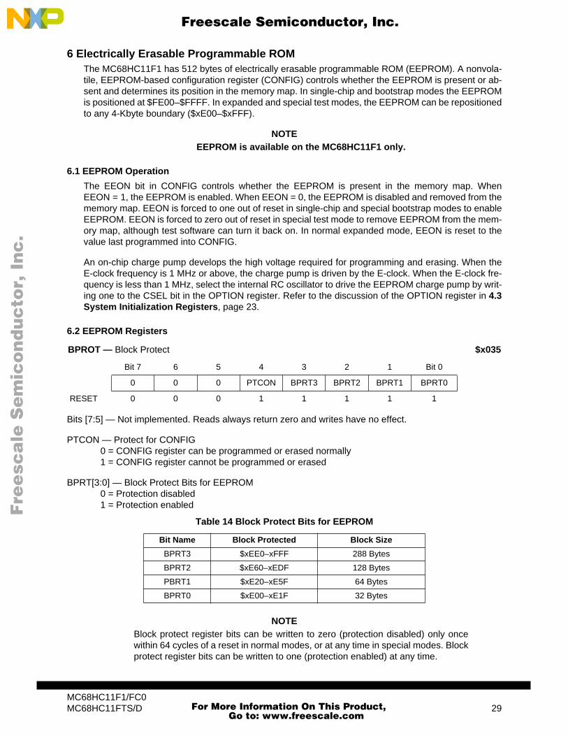
6 Electrically Erasable Programmable ROMThe MC68HC11F1 has 512 bytes of electrically erasable programmable ROM (EEPROM). A nonvola-tile, EEPROM-based configuration register (CONFIG) controls whether the EEPROM is present or ab-sent and determines its position in the memory map. In single-chip and bootstrap modes the EEPROMis positioned at $FE00–$FFFF. In expanded and special test modes, the EEPROM can be repositionedto any 4-Kbyte boundary ($xE00–$xFFF).
NOTEEEPROM is available on the MC68HC11F1 only.
6.1 EEPROM Operation
The EEON bit in CONFIG controls whether the EEPROM is present in the memory map. WhenEEON = 1, the EEPROM is enabled. When EEON = 0, the EEPROM is disabled and removed from thememory map. EEON is forced to one out of reset in single-chip and special bootstrap modes to enableEEPROM. EEON is forced to zero out of reset in special test mode to remove EEPROM from the mem-ory map, although test software can turn it back on. In normal expanded mode, EEON is reset to thevalue last programmed into CONFIG.
An on-chip charge pump develops the high voltage required for programming and erasing. When theE-clock frequency is 1 MHz or above, the charge pump is driven by the E-clock. When the E-clock fre-quency is less than 1 MHz, select the internal RC oscillator to drive the EEPROM charge pump by writ-ing one to the CSEL bit in the OPTION register. Refer to the discussion of the OPTION register in 4.3System Initialization Registers, page 23.
6.2 EEPROM Registers
Bits [7:5] — Not implemented. Reads always return zero and writes have no effect.
PTCON — Protect for CONFIG0 = CONFIG register can be programmed or erased normally1 = CONFIG register cannot be programmed or erased
BPRT[3:0] — Block Protect Bits for EEPROM0 = Protection disabled1 = Protection enabled
NOTEBlock protect register bits can be written to zero (protection disabled) only oncewithin 64 cycles of a reset in normal modes, or at any time in special modes. Blockprotect register bits can be written to one (protection enabled) at any time.
BPROT — Block Protect $x035
Bit 7 6 5 4 3 2 1 Bit 0
0 0 0 PTCON BPRT3 BPRT2 BPRT1 BPRT0
RESET 0 0 0 1 1 1 1 1
Table 14 Block Protect Bits for EEPROM
Bit Name Block Protected Block Size
BPRT3 $xEE0–xFFF 288 Bytes
BPRT2 $xE60–xEDF 128 Bytes
PBRT1 $xE20–xE5F 64 Bytes
BPRT0 $xE00–xE1F 32 Bytes
MC68HC11F1/FC0 MC68HC11FTS/D 29
For More Information On This Product,
Go to: www.freescale.com

F
ree
sca
le S
em
ico
nd
uc
tor,
I
Freescale Semiconductor, Inc.n
c..
.
ODD — Program Odd Rows (TEST)
EVEN — Program Even Rows (TEST)
ROW and BYTE — Row Erase Select Bit and Byte Erase SelectThe value of these bits determines the manner in which EEPROM is erased. Bit encodings are shownin 6.2 EEPROM Registers, page 30.
ERASE — Erase/Normal Control for EEPROM0 = Normal read or program mode1 = Erase mode
EELAT — EEPROM Latch Control0 = EEPROM address and data bus configured for normal reads1 = EEPROM address and data bus configured for programming or erasing
EEPGM — EEPROM Program Command0 = Program or erase voltage to EEPROM array switched off1 = Program or erase voltage to EEPROM array switched on
U = Unaffected by reset.
The CONFIG register is used to assign EEPROM a location in the memory map and to enable or disableEEPROM operation. Bits in this register are user-programmed except when forced to certain values, asnoted in the following bit descriptions.
EE[3:0] — EEPROM Map PositionEEPROM is located at $xE00 – $xFFF, where x is the value represented by these four bits. In single-chip and bootstrap modes, EEPROM is forced to $FE00 – $FFFF, regardless of the state of these bits.On factory-fresh devices, EE[3:0] = $0.
Bit 3 — Not implemented. Reads always return one and writes have no effect.
NOCOP — COP System Disable0 = COP enabled (forces reset on time-out)1 = COP disabled (does not force reset on time-out)
PPROG — EEPROM Programming Control $x03B
Bit 7 6 5 4 3 2 1 Bit 0
ODD EVEN 0 BYTE ROW ERASE EELAT EEPGM
RESET 0 0 0 0 0 0 0 0
Table 15 ROW and BYTE Encodings
BYTE ROW Action
0 0 Bulk Erase (All 512 Bytes)
0 1 Row Erase (16 Bytes)
1 0 Byte Erase
1 1 Byte Erase
CONFIG — EEPROM Mapping, COP, EEPROM Enables $x03F
Bit 7 6 5 4 3 2 1 Bit 0
EE3 EE2 EE1 EE0 1 NOCOP 1 EEON
RESET U U U U 1 U 1 U
MC68HC11F1/FC030 MC68HC11FTS/D
For More Information On This Product,
Go to: www.freescale.com

F
ree
sca
le S
em
ico
nd
uc
tor,
I
Freescale Semiconductor, Inc.n
c..
.
Bit 1 — Not implemented. Reads always return one and writes have no effect.
EEON — EEPROM EnableThis bit is forced to one in single-chip and bootstrap modes. In test mode, EEON is forced to zero outof reset. In expanded mode, the EEPROM obeys the state of this bit.
0 = EEPROM is removed from the memory map.1 = EEPROM is present in the memory map.
Refer to 6.4 CONFIG Register Programming for instructions on programming this register.
6.3 EEPROM Programming and Erasure
Programming and erasing the EEPROM is controlled by the PPROG register, subject to the block pro-tect (BPROT) register value. To erase the EEPROM, ensure that the proper bits of the BPROT registerare cleared, and then complete the following steps:
1. Write to PPROG with the ERASE and EELAT bits set and the BYTE and ROW bits set orcleared as appropriate.
2. Write to the appropriate EEPROM address with any data. Row erase ($xE00–$xE0F, $xE10–$xE1F,... $xFF0–$xFFF) requires a single write to any location in the row. Perform bulk eraseby writing to any location in the array.
3. Write to PPROG with the ERASE, EELAT, and EEPGM bits set and the BYTE and ROW bitsset or cleared as appropriate.
4. Delay for 10 ms (20 ms for low-voltage operation).5. Clear the EEPGM bit in PPROG to turn off the high voltage.6. Clear the PPROG register to reconfigure EEPROM address and data buses for normal opera-
tions.
To program the EEPROM, ensure that the proper bits of the BPROT register are cleared, and then com-plete the following steps:
1. Write to PPROG with the EELAT bit set.2. Write data to the desired address.3. Write to PPROG with the EELAT and EEPGM bits set.4. Delay for 10 ms (20 ms for low-voltage operation).5. Clear the EEPGM bit in PPROG to turn off the high voltage.6. Clear the PPROG register to reconfigure EEPROM address and data buses for normal opera-
tions.
6.3.1 Programming a Byte
The following example shows how to program an EEPROM byte. This example assumes that the ap-propriate bits in BPROT are cleared and that the data to be programmed is present in accumulator A.
PROG LDAB #$02 EELAT=1, EEPGM=0STAB $103B Set EELAT bitSTAA $FE00 Store data to EEPROM addressLDAB #$03 EELAT=1, EEPGM=1STAB $103B Turn on programming voltageJSR DLY10 Delay 10 msCLR $103B Turn off high voltage and set to READ mode
6.3.2 Bulk Erase
The following example shows how to bulk erase the 512-byte EEPROM. The CONFIG register is notaffected in this example. Note that when the CONFIG register is bulk erased, CONFIG and the 512-bytearray are all erased.
BULKE LDAB #$06 ERASE=1, EELAT=1, EEPGM=0STAB $103B Set EELAT bit
MC68HC11F1/FC0 MC68HC11FTS/D 31
For More Information On This Product,
Go to: www.freescale.com

F
ree
sca
le S
em
ico
nd
uc
tor,
I
Freescale Semiconductor, Inc.n
c..
.
STAB $FE00 Store any data to any EEPROM addressLDAB #$07 EELAT=1, EEPGM=1STAB $103B Turn on programming voltageJSR DLY10 Delay 10 msCLR $103B Turn off high voltage and set to READ mode
6.3.3 Row Erase
The following example shows how to perform a fast erase of large sections of EEPROM. This exampleassumes that index register X contains the address of a location in the desired row.
ROWE LDAB #$0E ROW=1, ERASE=1, EELAT=1, EEPGM=0STAB $103B Set to ROW erase modeSTAB $xxxx Store any data to any address in ROWLDAB #$0F ROW=1, ERASE=1, EELAT=1, EEPGM=1STAB $103B Turn on high voltageJSR DLY10 Delay 10 msCLR $103B Turn off high voltage and set to READ mode
6.3.4 Byte Erase
The following is an example of how to erase a single byte of EEPROM. This example assumes that in-dex register X contains the address of the byte to be erased.
BYTEE LDAB #$16 BYTE=1, ROW=0, ERASE=1, EELAT=1, EEPGM=0STAB $103B Set to BYTE erase modeSTAB $0,X Store any data to address to be erasedLDAB #$17 BYTE=1, ROW=0, ERASE=1, EELAT=1, EEPGM=1STAB $103B Turn on high voltageJSR DLY10 Delay 10 msCLR $103B Turn off high voltage and set to READ mode
6.4 CONFIG Register Programming
Because the CONFIG register is implemented with EEPROM cells, use EEPROM procedures to eraseand program this register. The procedure for programming is the same as for programming a byte inthe EEPROM array, except that the CONFIG register address is used. CONFIG can be programmed orerased (including byte erase) while the MCU is operating in any mode, provided that PTCON in BPROTis clear. To change the value in the CONFIG register, complete the following procedure. Do not initiatea reset until the procedure is complete. The new value will not take effect until after the next reset se-quence.
1. Erase the CONFIG register.2. Program the new value to the CONFIG address. 3. Initiate reset.
MC68HC11F1/FC032 MC68HC11FTS/D
For More Information On This Product,
Go to: www.freescale.com

F
ree
sca
le S
em
ico
nd
uc
tor,
I
Freescale Semiconductor, Inc.n
c..
.
7 Parallel Input/Output On the MC68HC11F1, either 54 or 51 pins are available for general-purpose I/O, depending on thepackage. These pins are arranged into ports A, B, C, D, E, F, and G. On the MC68HC11FC0, either 52or 49 pins are available, depending on the package.
I/O functions on some ports (B, C, F, and G) are affected by the mode of operation selected. In the sin-gle-chip and bootstrap modes, they are configured as parallel I/O data ports. In expanded and testmodes, they are configured as follows:
• Ports B and F are configured as the address bus.• Port C is configured as the data bus.• Port G bit 7 is configured as the optional program chip select CSPROG.
In addition, in expanded and test modes the R/W signal is configured as data bus direction control. Theremaining ports (A, D, and E) are unaffected by mode changes.
7.1 Port A
Port A is an eight-bit general-purpose I/O port (PA[7:0]) with a data register (PORTA) and a data direc-tion register (DDRA). Port A pins are available for shared use among the main timer, pulse accumulator,and general I/O functions, regardless of mode. Four pins can be used for timer output compare func-tions (OC), three for input capture (IC), and one as either a fourth IC or a fifth OC.
7.2 Port B
Port B is an eight-bit general-purpose output-only port in single-chip modes. In expanded modes, portB pins act as high-order address lines ADDR[15:8], and accesses to PORTB (the port B data register)are mapped externally.
7.3 Port C
Port C is an eight-bit general-purpose I/O port with a data register (PORTC) and a data direction register(DDRC). In single-chip modes, port C pins are general-purpose I/O pins PC[7:0]. Port C can be config-ured for wired-OR operation in single-chip modes by setting the CWOM bit in the OPT2 register. In ex-panded modes, port C is the data bus DATA[7:0], and accesses to PORTC (the port C data register)are mapped externally.
7.4 Port D
Port D is a six-bit general-purpose I/O port with a data register (PORTD) and a data direction register(DDRD). In all modes, the six port D lines (PD[5:0]) can be used for general-purpose I/O or for the serialcommunications interface (SCI) or serial peripheral interface (SPI) subsystems. Port D can also be con-figured for wired-OR operation.
7.5 Port E
Port E is an eight-bit input-only port that is also used (on the MC68HC11F1 only) as the analog inputport for the analog-to-digital converter. Port E pins that are not used for the A/D system can be used asgeneral-purpose inputs. However, PORTE should not be read during the sample portion of an A/D con-version sequence.
NOTEPE7 and PE0 are not available on the 80-pin MC68HC11FC0. PE7, PE4, and PE0are not available on the 64-pin MC68HC11FC0.
7.6 Port F
Port F is an eight-bit output-only port. In single-chip mode, port F pins are general-purpose output pinsPF[7:0]. In expanded mode, port F pins act as low-order address outputs ADDR[7:0].
MC68HC11F1/FC0 MC68HC11FTS/D 33
For More Information On This Product,
Go to: www.freescale.com

F
ree
sca
le S
em
ico
nd
uc
tor,
I
Freescale Semiconductor, Inc.n
c..
.
7.7 Port G
Port G is an eight-bit general-purpose I/O port with a data register (PORTG) and a data direction register(DDRG). When enabled, the upper four lines (PG[7:4] can be used as chip-select outputs in expandedmodes. When any of these pins are not being used for chip selects, they can be used for general-pur-pose I/O. Port G can be configured for wired-OR operation by setting the GWOM bit in the OPT2 reg-ister.
NOTEPG[1:0] are not available on the 64-pin MC68HC11FC0.
7.8 Parallel I/O Registers
Port pin function is mode dependent. Do not confuse pin function with the electrical state of the pin atreset. Port pins are either driven to a specified logic level or are configured as high impedance inputs.I/O pins configured as high-impedance inputs have port data that is indeterminate. The contents of thecorresponding latches are dependent upon the electrical state of the pins during reset. In port descrip-tions, an “I” indicates this condition. Port pins that are driven to a known logic level during reset areshown with a value of either one or zero. Some control bits are unaffected by reset. Reset states forthese bits are indicated with a “U”.
I = Indeterminate value
For DDRx bits, 0 = input and 1 = output.
*These bits are not present on the 64-pin QFP version of the MC68HC11FC0.I = Indeterminate value
PORTA — Port A Data Register $x000
Bit 7 6 5 4 3 2 1 Bit 0
PA7 PA6 PA5 PA4 PA3 PA2 PA1 PA0
RESET: I I I I I I I I
Alternate Function: PAI OC2 OC3 OC4 OC5/IC4 IC1 IC2 IC3
And/or: OC1 OC1 OC1 OC1 OC1 — — —
DDRA — Port A Data Direction Register $x001
Bit 7 6 5 4 3 2 1 Bit 0
DDA7 DDA6 DDA5 DDA4 DDA3 DDA2 DDA1 DDA0
RESET: 0 0 0 0 0 0 0 0
PORTG — Port G Data Register $x002
Bit 7 6 5 4 3 2 1 Bit 0
PG7 PG6 PG5 PG4 PG3 PG2 PG1* PG0*
RESET: I I I I I I I I
Alternate Function: CSPROG CSGEN CSIO1 CSIO2
MC68HC11F1/FC034 MC68HC11FTS/D
For More Information On This Product,
Go to: www.freescale.com

F
ree
sca
le S
em
ico
nd
uc
tor,
I
Freescale Semiconductor, Inc.n
c..
.
* Following reset in expanded and test modes, PG7/CSPRG is configured as a program chip select, forcing the pinto be an output pin, even though the value of the DDG7 bit remains zero.
For DDRx bits, 0 = input and 1 = output.
The reset state of port B is mode dependent. In single-chip or bootstrap modes, port B pins are general-purpose outputs. In expanded and test modes, port B pins are high-order address outputs and PORTBis not in the memory map.
The reset state of port F is mode dependent. In single-chip or bootstrap modes, port F pins are general-purpose outputs. In expanded and test modes, port F pins are low-order address outputs and PORTFis not in the memory map.
The reset state of port C is mode dependent. In single-chip and bootstrap modes, port C pins are high-impedance inputs. In expanded or test modes, port C pins are data bus inputs/outputs and PORTC isnot in the memory map. The R/W signal is used to control the direction of data transfers.
For DDRx bits, 0 = input and 1 = output.
DDRG — Port G Data Direction Register $x003
Bit 7 6 5 4 3 2 1 Bit 0
DDG7* DDG6 DDG5 DDG4 DDG3 DDG2 DDG1 DDG0
RESET: 0 0 0 0 0 0 0 0
PORTB — Port B Data Register $x004
Bit 7 6 5 4 3 2 1 Bit 0
PB7 PB6 PB5 PB4 PB3 PB2 PB1 PB0
RESET: 0 0 0 0 0 0 0 0
Alternate Function: ADDR15 ADDR14 ADDR13 ADDR12 ADDR11 ADDR10 ADDR9 ADDR8
PORTF — Port F Data Register $x005
PF7 PF6 PF5 PF4 PF3 PF2 PF1 PF0
RESET: 0 0 0 0 0 0 0 0
Alternate Function: ADDR7 ADDR6 ADDR5 ADDR4 ADDR3 ADDR2 ADDR1 ADDR0
PORTC — Port C Data Register $x006
Bit 7 6 5 4 3 2 1 Bit 0
PC7 PC6 PC5 PC4 PC3 PC2 PC1 PC0
RESET: I I I I I I I I
Alternate Function: DATA7 DATA6 DATA5 DATA4 DATA3 DATA2 DATA1 DATA0
DDRC — Port C Data Direction Register $x007
Bit 7 6 5 4 3 2 1 Bit 0
DDC7 DDC6 DDC5 DDC4 DDC3 DDC2 DDC1 DDC0
RESET: 0 0 0 0 0 0 0 0
MC68HC11F1/FC0 MC68HC11FTS/D 35
For More Information On This Product,
Go to: www.freescale.com
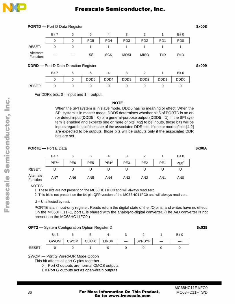
F
ree
sca
le S
em
ico
nd
uc
tor,
I
Freescale Semiconductor, Inc.n
c..
.
For DDRx bits, 0 = input and 1 = output.NOTEWhen the SPI system is in slave mode, DDD5 has no meaning or effect. When theSPI system is in master mode, DDD5 determines whether bit 5 of PORTD is an er-ror detect input (DDD5 = 0) or a general-purpose output (DDD5 = 1). If the SPI sys-tem is enabled and expects one or more of bits [4:2] to be inputs, those bits will beinputs regardless of the state of the associated DDR bits. If one or more of bits [4:2]are expected to be outputs, those bits will be outputs only if the associated DDRbits are set.
U = Unaffected by rest.
PORTE is an input-only register. Reads return the digital state of the I/O pins, and writes have no effect.On the MC68HC11F1, port E is shared with the analog-to-digital converter. (The A/D converter is notpresent on the MC68HC11FC0.)
GWOM — Port G Wired-OR Mode OptionThis bit affects all port G pins together.
0 = Port G outputs are normal CMOS outputs1 = Port G outputs act as open-drain outputs
NOTES:1. These bits are not present on the MC68HC11FC0 and will always read zero.2. This bit is not present on the 64-pin QFP version of the MC68HC11FC0 and will always read zero.
PORTD — Port D Data Register $x008
Bit 7 6 5 4 3 2 1 Bit 0
0 0 PD5 PD4 PD3 PD2 PD1 PD0
RESET: 0 0 I I I I I I
Alternate Function: — — SS SCK MOSI MISO TxD RxD
DDRD — Port D Data Direction Register $x009
Bit 7 6 5 4 3 2 1 Bit 0
0 0 DDD5 DDD4 DDD3 DDD2 DDD1 DDD0
RESET: 0 0 0 0 0 0 0 0
PORTE — Port E Data $x00A
Bit 7 6 5 4 3 2 1 Bit 0
PE71 PE6 PE5 PE42 PE3 PE2 PE1 PE01
RESET: U U U U U U U U
Alternate Function
AN7 AN6 AN5 AN4 AN3 AN2 AN1 AN0
OPT2 — System Configuration Option Register 2 $x038
Bit 7 6 5 4 3 2 1 Bit 0
GWOM CWOM CLK4X LIRDV — SPRBYP — —
RESET 0 0 1 0 0 0 0 0
MC68HC11F1/FC036 MC68HC11FTS/D
For More Information On This Product,
Go to: www.freescale.com

F
ree
sca
le S
em
ico
nd
uc
tor,
I
Freescale Semiconductor, Inc.n
c..
.
CWOM — Port C Wired-OR Mode OptionThis bit affects all port C pins together.
0 = Port C outputs are normal CMOS outputs1 = Port C outputs act as open-drain outputs
CLK4X — 4XCLK Output EnableRefer to 4.3 System Initialization Registers, page 23
LIRDV — Load Instruction Register DrivenRefer to 4.3 System Initialization Registers, page 23
Bits 3, 1, 0 — Not implemented. Reads always return zero and writes have no effect.
SPRBYP — Refer to 10.2 SPI Registers, page 52.
MC68HC11F1/FC0 MC68HC11FTS/D 37
For More Information On This Product,
Go to: www.freescale.com

F
ree
sca
le S
em
ico
nd
uc
tor,
I
Freescale Semiconductor, Inc.n
c..
.
8 Chip-SelectsChip selects eliminate the need for additional external components to interface with peripherals in ex-panded non-multiplexed modes. Chip-select registers control polarity, address block size, base ad-dress, and clock stretching.
8.1 Chip-Select Operation
There are four programmable chip selects on the MC68HC11F1 and MC68HC11FC0: two for externalI/O (CSIO1 and CSIO2), one for external program space (CSPROG), and one general-purpose chip se-lect (CSGEN).
CSPROG is active low and becomes active at address valid time. CSPROG is enabled by the PCSENbit of the chip-select control register (CSCTL). Its address block size is selected by the PSIZA andPSIZB bits of CSCTL.
Use the I/O chip selects (CSIO1 and CSIO2) for external I/O devices. These chip-select addresses arefound in the memory map block that contains the status and control registers. CSIO1 is mapped from$x060 to $x7FF, and CSIO2 is mapped from $x800 to $xFFF, where x represents the REG[3:0] bits ofthe INIT register on the MC68HC11F1 or the REG[1:0] bits of the INIT register on the MC68HC11FC0.Polarity and enable-disable selections are controlled by CSCTL register bits IO1EN, IO1PL, IO2EN, andIO2PL. The IO1AV and IO2AV bits of the CSGSIZ register determine whether the chip selects are validduring address or E-clock valid times.
The general-purpose chip select is the most flexible of the four chip selects. Polarity, valid assertiontime, and block size are determined by the GNPOL, GAVLD, GSIZA, GSIZB, and GSIZC bits of theCSGSIZ register. The starting address is selected with the CSGADR register.
Each of the four chip selects has two associated bits in the chip-select clock stretch register (CSSTRH).These bits allow clock stretching from zero to three cycles (full E-clock periods) to accommodate slowdevice interfaces. Any of the chip selects can be programmed to cause a clock stretch to occur onlyduring access to addresses that fall within that particular chip select’s address range.
During the stretch period, the E-clock is held high and the bus remains in the state that it is normally inat the end of E high time. Internally, the clocks continue to run, which maintains the integrity of the timersand baud-rate generators.
Priority levels are assigned to prevent the four chip selects from conflicting with each other or with in-ternal memory and registers. There are two sets of priorities controlled by the value of the general-pur-pose chip-select priority bit (GCSPR) of the CSCTL register. Refer to Table 17.
8.2 Chip-Select Registers
IO1SA, IOS1B — I/O Chip-Select 1 Clock Stretch
IO2SA, IO2SB — I/O Chip-Select 2 Clock Stretch
GSTHA, GSTHB — General-Purpose Chip-Select Clock Stretch
PSTHA, PSSTHB — Program Chip-Select Clock StretchEach pair of bits selects the number of clock cycles of stretch for the corresponding chip select.
CSSTRH — Clock Stretching $x05C
Bit 7 6 5 4 3 2 1 Bit 0
IO1SA IO1SB IO2SA IO2SB GSTHA GSTHB PSTHA PSTHB
RESET: 0 0 0 0 0 0 0 0
MC68HC11F1/FC038 MC68HC11FTS/D
For More Information On This Product,
Go to: www.freescale.com

F
ree
sca
le S
em
ico
nd
uc
tor,
I
Freescale Semiconductor, Inc.n
c..
.
* PCSEN is set out of reset in expanded modes and cleared in single-chip modes.
IO1EN — I/O Chip-Select 1 Enable 0 = CSIO1 disabled1 = CSIO1 enabled
IO1PL — I/O Chip-Select 1 Polarity 0 = CSIO1 active low1 = CSIO1 active high
IO1EN — I/O Chip-Select 2 Enable0 = CSIO2 disabled1 = CSIO2 enabled
IO2PL — I/O Chip-Select 2 Polarity 0 = CSIO2 active low1 = CSIO2 active high
GCSPR — General-Purpose Chip-Select Priority0 = Program chip-select has priority over general-purpose chip-select1 = General-purpose chip-select has priority over program chip-select
Refer to Table 17.
NOTES:1. EEPROM is present on the MC68HC11F1 only.
Table 16 Chip Select Clock Stretch Control
Clock Stretch Bits A, B
Clock Stretch
0 0 0 Cycles
0 1 1 Cycle
1 0 2 Cycles
1 1 3 Cycles
CSCTL — Chip-Select Control $x05D
Bit 7 6 5 4 3 2 1 Bit 0
IO1EN IO1PL IO2EN IO2PL GCSPR PCSEN* PSIZA PSIZB
RESET: 0 0 0 0 0 — 0 0
Table 17 Chip Select Priorities
GCSPR = 0 GCSPR = 1
On-Chip Registers On-Chip Registers
On-Chip RAM On-Chip RAM
Bootloader ROM Bootloader ROM
On-Chip EEPROM1 On-Chip EEPROM1
I/O Chip Selects I/O Chip Selects
Program Chip Select General-Purpose Chip Select
General-Purpose Chip Select Program Chip Select
MC68HC11F1/FC0 MC68HC11FTS/D 39
For More Information On This Product,
Go to: www.freescale.com

F
ree
sca
le S
em
ico
nd
uc
tor,
I
Freescale Semiconductor, Inc.n
c..
.
PCSEN — Program Chip-Select EnableReset clears PCSEN in single-chip modes and sets PCSEN in expanded modes.
0 = CSPROG disabled1 = CSPROG enabled
PSIZA, PSIZB — Select Size of Program Chip-Select
GA[15:10] — General-Purpose Chip-Select Starting AddressThese bits determine the starting address of the CSGEN valid address space and correspond to thehigh-order address bits ADDR[15:10]. Table 19 illustrates how the block size selected determineswhich of this register's bits are valid.
Bits [1:0] — Not implemented. Reads always return zero and writes have no effect.
IO1AV — I/O Chip-Select 1 Address Valid0 = CSIO1 is valid during E-clock valid time (E-clock high)1 = CSIO1 is valid during address valid time
IO2AV — I/O Chip-Select 2 Address Valid0 = CSIO2 is valid during E-clock valid time (E-clock high)1 = CSIO2 is valid during address valid time
Table 18 Program Chip Select Size Control
PSIZA PSIZB Size Address Range
0 0 64 Kbytes $0000–$FFFF
0 1 32 Kbytes $8000–$FFFF
1 0 16 Kbytes $C000–$FFFF
1 1 8 Kbytes $E000–$FFFF
CSGADR — General-Purpose Chip-Select Address Register $x05E
Bit 7 6 5 4 3 2 1 Bit 0
GA15 GA14 GA13 GA12 GA11 GA10 — —
RESET: 0 0 0 0 0 0 0 0
Table 19 General Purpose Chip Select Starting Address
CSGEN Block Size CSGADR Bits Valid
0 Kbytes None
1 Kbyte GA15 – GA10
2 Kbytes GA15 – GA11
4 Kbytes GA15 – GA12
8 Kbytes GA15 – GA13
16 Kbytes GA15 – GA14
32 Kbytes GA15
64 Kbytes None
CSGSIZ — General-Purpose Chip-Select Size Register $x05F
Bit 7 6 5 4 3 2 1 Bit 0
IO1AV IO2AV — GNPOL GAVLD GSIZA GSIZB GSIZC
RESET: 0 0 0 0 0 1 1 1
MC68HC11F1/FC040 MC68HC11FTS/D
For More Information On This Product,
Go to: www.freescale.com

F
ree
sca
le S
em
ico
nd
uc
tor,
I
Freescale Semiconductor, Inc.n
c..
.
Bit 5 — Not implemented. Reads always return zero and writes have no effect.
GNPOL — General-Purpose Chip-Select Polarity 0 = CSGEN is active low1 = CSGEN is active high
GAVLD — General-Purpose Chip-Select Address Valid 0 = CSGEN is valid during E-clock valid time (E-clock high)1 = CSGEN is valid during address valid time
GSIZ[A:C] — Block Size for CSGENRefer to Table 20 for bit values.
Table 20 General-Purpose Chip Select Size Control
GSIZ[A:C] Address Size
000 64 Kbytes
001 32 Kbytes
010 16 Kbytes
011 8 Kbytes
100 4 Kbytes
101 2 Kbytes
110 1 Kbyte
111 0 Kbytes (disabled)
MC68HC11F1/FC0 MC68HC11FTS/D 41
For More Information On This Product,
Go to: www.freescale.com

F
ree
sca
le S
em
ico
nd
uc
tor,
I
Freescale Semiconductor, Inc.n
c..
.
9 Serial Communications Interface (SCI)The SCI, a universal asynchronous receiver transmitter (UART) serial communications interface, is oneof two independent serial I/O subsystems in the MC68HC11F1 and MC68HC11FC0. The SCI has astandard non-return to zero (NRZ) format (one start bit, eight or nine data bits, and one stop bit) andseveral selectable baud rates. The transmitter and receiver are independent but use the same data for-mat and bit rate.
9.1 SCI Block Diagrams
Figure 9 SCI Transmitter Block Diagram
TCTDR
E
SCSR1 SCI STATUS 1
SCCR2 SCI CONTROL 2
TRANSMITTERCONTROL LOGIC
TCIE
TC
TIE
TDRE
SCI RxQUESTS
SCI INTERRUPTREQUEST
INTERNALDATA BUS
PIN BUFFERAND CONTROLH
10 (11) - BIT Tx SHIFT REGISTER
DDD1 SCDR Tx BUFFER
TRAN
SFER
Tx
BUFF
ER
SHIF
T EN
ABLE
JAM
EN
ABLE
PREA
MBL
E—JA
M 1
s
BREA
K—JA
M 0
s
(WRITE ONLY)
FORCE PINDIRECTION (OUT)
SIZE
8/9
M
SCCR1 SCI CONTROL 1
TRANSMITTERBAUD RATE
CLOCK
TIE
TCIE
TE SBK
(8) 7 6 5 4 3 2 1 0 L PD1TxD
T8R8
WAK
E
RD
RF
IDLE
OR
NF
FER
IE
ILIE
RE
RW
U
MC68HC11F1/FC042 MC68HC11FTS/D
For More Information On This Product,
Go to: www.freescale.com
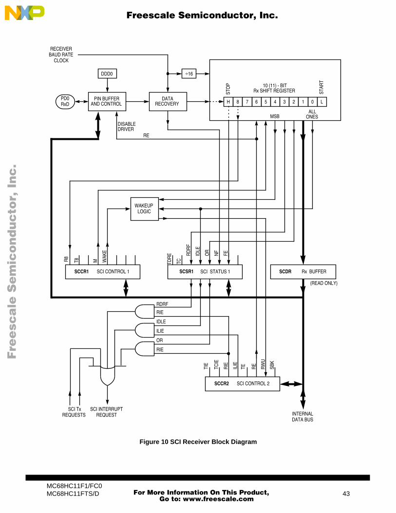
F
ree
sca
le S
em
ico
nd
uc
tor,
I
Freescale Semiconductor, Inc.n
c..
.
Figure 10 SCI Receiver Block Diagram
SCSR1 SCI STATUS 1
SCCR2 SCI CONTROL 2
SCI TxREQUESTS
SCI INTERRUPTREQUEST INTERNAL
DATA BUS
H
10 (11) - BIT
M
SCCR1 SCI CONTROL 1
RECEIVERBAUD RATE
CLOCK
RIE
ILIE
8 7 6 5 4 3 2 1 0 LPD0RxD
SCDR Rx BUFFER
Rx SHIFT REGISTER
DDD0
PIN BUFFERAND CONTROL
DATARECOVERY
÷16
STO
P
STAR
T
MSBALL
ONES
RE
WAKEUPLOGIC
RD
RF
IDLE
OR
NF
FE
RW
U
DISABLEDRIVER
WAK
E
(READ ONLY)
RDRF
RIE
IDLE
ILIE
OR
RIE
R8
T8 TDR
E
RE
TC
TIE
TCIE
TE SBK
MC68HC11F1/FC0 MC68HC11FTS/D 43
For More Information On This Product,
Go to: www.freescale.com
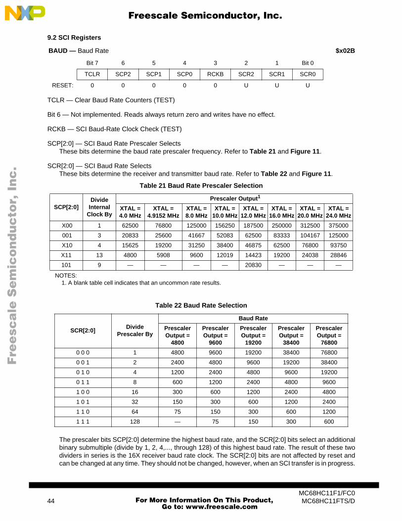
F
ree
sca
le S
em
ico
nd
uc
tor,
I
Freescale Semiconductor, Inc.n
c..
.
9.2 SCI Registers
TCLR — Clear Baud Rate Counters (TEST)
Bit 6 — Not implemented. Reads always return zero and writes have no effect.
RCKB — SCI Baud-Rate Clock Check (TEST)
SCP[2:0] — SCI Baud Rate Prescaler SelectsThese bits determine the baud rate prescaler frequency. Refer to Table 21 and Figure 11.
SCR[2:0] — SCI Baud Rate SelectsThese bits determine the receiver and transmitter baud rate. Refer to Table 22 and Figure 11.
The prescaler bits SCP[2:0] determine the highest baud rate, and the SCR[2:0] bits select an additionalbinary submultiple (divide by 1, 2, 4,..., through 128) of this highest baud rate. The result of these twodividers in series is the 16X receiver baud rate clock. The SCR[2:0] bits are not affected by reset andcan be changed at any time. They should not be changed, however, when an SCI transfer is in progress.
NOTES:1. A blank table cell indicates that an uncommon rate results.
BAUD — Baud Rate $x02B
Bit 7 6 5 4 3 2 1 Bit 0
TCLR SCP2 SCP1 SCP0 RCKB SCR2 SCR1 SCR0
RESET: 0 0 0 0 0 U U U
Table 21 Baud Rate Prescaler Selection
SCP[2:0]Divide
Internal Clock By
Prescaler Output1
XTAL = 4.0 MHz
XTAL = 4.9152 MHz
XTAL = 8.0 MHz
XTAL = 10.0 MHz
XTAL = 12.0 MHz
XTAL = 16.0 MHz
XTAL = 20.0 MHz
XTAL = 24.0 MHz
X00 1 62500 76800 125000 156250 187500 250000 312500 375000
001 3 20833 25600 41667 52083 62500 83333 104167 125000
X10 4 15625 19200 31250 38400 46875 62500 76800 93750
X11 13 4800 5908 9600 12019 14423 19200 24038 28846
101 9 — — — — 20830 — — —
Table 22 Baud Rate Selection
SCR[2:0]Divide
Prescaler By
Baud Rate
Prescaler Output =
4800
Prescaler Output =
9600
Prescaler Output =
19200
Prescaler Output =
38400
Prescaler Output =
76800
0 0 0 1 4800 9600 19200 38400 76800
0 0 1 2 2400 4800 9600 19200 38400
0 1 0 4 1200 2400 4800 9600 19200
0 1 1 8 600 1200 2400 4800 9600
1 0 0 16 300 600 1200 2400 4800
1 0 1 32 150 300 600 1200 2400
1 1 0 64 75 150 300 600 1200
1 1 1 128 — 75 150 300 600
MC68HC11F1/FC044 MC68HC11FTS/D
For More Information On This Product,
Go to: www.freescale.com

F
ree
sca
le S
em
ico
nd
uc
tor,
I
Freescale Semiconductor, Inc.n
c..
.
Figure 11 illustrates the SCI baud rate timing chain. The prescaler select bits determine the highestbaud rate. The rate select bits determine additional divide-by-two stages to arrive at the receiver timing(RT) clock rate. The baud rate clock is the result of dividing the RT clock by 16.
Figure 11 SCI Baud Rate Generator Block Diagram
OSCILLATORAND
CLOCK GENERATOR
(÷4)XTAL
EXTAL
E
INTERNAL BUS CLOCK (PH2)
SCR[2:0]
÷ 3
X00 001
÷ 4
X10
÷ 13
X11
0:0:0
÷ 2 0:0:1
÷ 2 0:1:0
÷ 2 0:1:1
÷ 2 1:0:1
÷ 2 1:0:0
÷ 2 1:1:1
÷ 2 1:1:0
÷ 16
SCI Receive Baud Rate (16x)
SCI Transmit Baud Rate (1x)
÷ 9
101
MC68HC11F1/FC0 MC68HC11FTS/D 45
For More Information On This Product,
Go to: www.freescale.com

F
ree
sca
le S
em
ico
nd
uc
tor,
I
Freescale Semiconductor, Inc.n
c..
.
U = Unaffected by reset
R8 — Receive Data Bit 8If M is set, R8 stores the ninth bit of the receive data character.
T8 — Transmit Data Bit 8If M is set, T8 stores the ninth bit of the transmit data character.
Bit 5 — Not implemented. Reads always return zero and writes have no effect.
M — Mode (Select Character Format)0 = 1 start bit, 8 data bits, 1 stop bit1 = 1 start bit, 9 data bits, 1 stop bit
WAKE — Wake Up by Address Mark/Idle0 = Wake up by IDLE line recognition1 = Wake up by address mark
Bits [2:0] — Not implemented. Reads always return zero and writes have no effect.
TIE — Transmit Interrupt Enable0 = TDRE interrupts disabled1 = SCI interrupt requested when the TDRE flag is set
TCIE — Transmit Complete Interrupt Enable0 = TC interrupts disabled1 = SCI interrupt requested when the TC flag is set
RIE — Receiver Interrupt Enable0 = RDRF and OR interrupts disabled1 = SCI interrupt requested when the RDRF flag or the OR flag is set
ILIE — Idle Line Interrupt Enable0 = IDLE interrupts disabled 1 = SCI interrupt requested when IDLE status flag is set
TE — Transmitter EnableWhen TE goes from zero to one, one unit of idle character time (logic one) is queued as a preamble.
0 = Transmitter disabled1 = Transmitter enabled
RE — Receiver Enable0 = Receiver disabled1 = Receiver enabled
SCCR1 — SCI Control Register 1 $x02C
Bit 7 6 5 4 3 2 1 Bit 0
R8 T8 0 M WAKE 0 0 0
RESET: U U 0 0 0 0 0 0
SCCR2 — SCI Control Register 2 $x02D
Bit 7 6 5 4 3 2 1 Bit 0
TIE TCIE RIE ILIE TE RE RWU SBK
RESET: 0 0 0 0 0 0 0 0
MC68HC11F1/FC046 MC68HC11FTS/D
For More Information On This Product,
Go to: www.freescale.com

F
ree
sca
le S
em
ico
nd
uc
tor,
I
Freescale Semiconductor, Inc.n
c..
.
RWU — Receiver Wake Up Control0 = Normal SCI receiver1 = Wake up enabled and receiver interrupt inhibited
SBK — Send Break0 = Break generator off1 = Break codes generated as long as SBK = 1
TDRE — Transmit Data Register Empty FlagThis flag is set when SCDR is empty. Clear the TDRE flag by reading SCSR with TDRE set and thenwriting to SCDR.
0 = SCDR is busy1 = SCDR is empty
TC — Transmit Complete FlagThis flag is set when the transmitter is idle (no data, preamble, or break transmission in progress). Clearthe TC flag by reading SCSR with TC set and then writing to SCDR.
0 = Transmitter is busy1 = Transmitter is idle
RDRF — Receive Data Register Full FlagThis flag is set if a received character is ready to be read from SCDR. Clear the RDRF flag by readingSCSR with RDRF set and then reading SCDR.
0 = SCDR empty1 = SCDR full
IDLE — Idle Line Detected FlagThis flag is set if the RxD line is idle. Once cleared, IDLE is not set again until the RxD line has beenactive and becomes idle again. The IDLE flag is inhibited when RWU = 1. Clear IDLE by reading SCSRwith IDLE set and then reading SCDR.
0 = RxD line is active1 = RxD line is idle
OR — Overrun Error FlagOR is set if a new character is received before a previously received character is read from SCDR. ClearOR by reading SCSR with OR set and then reading SCDR.
0 = No overrun detected1 = Overrun detected
NF — Noise Error FlagNF is set if majority sample logic detects anything other than a unanimous decision. Clear NF by readingSCSR with NF set and then reading SCDR.
0 = Unanimous decision1 = Noise detected
FE — Framing ErrorFE is set when a zero is detected where a stop bit was expected. Clear the FE flag by reading SCSRwith FE set and then reading SCDR.
0 = Stop bit detected1 = Zero detected
SCSR — SCI Status Register $x02E
Bit 7 6 5 4 3 2 1 Bit 0
TDRE TC RDRF IDLE OR NF FE 0
RESET: 1 1 0 0 0 0 0 0
MC68HC11F1/FC0 MC68HC11FTS/D 47
For More Information On This Product,
Go to: www.freescale.com

F
ree
sca
le S
em
ico
nd
uc
tor,
I
Freescale Semiconductor, Inc.n
c..
.
Bit 0 — Not implemented. Reads always return zero and writes have no effect.
I = Indeterminate value
Reading SCDR retrieves the last byte received in the receive data buffer. Writing to SCDR loads thetransmit data buffer with the next byte to be transmitted.
SCDR — Serial Communications Data Register $x02F
Bit 7 6 5 4 3 2 1 Bit 0
Bit 7 6 5 4 3 2 2 Bit 0
RESET: I I I I I I I I
MC68HC11F1/FC048 MC68HC11FTS/D
For More Information On This Product,
Go to: www.freescale.com

F
ree
sca
le S
em
ico
nd
uc
tor,
I
Freescale Semiconductor, Inc.n
c..
.
10 Serial Peripheral InterfaceThe serial peripheral interface (SPI) allows the MCU to communicate synchronously with peripheral de-vices and other microprocessors. The SPI protocol facilitates rapid exchange of serial data between de-vices in a control system. The MC68HC11F1 and MC68HC11FC0 can be set up for master or slaveoperation. Standard data rates can be as high as one half of the E-clock rate when configured as mas-ter, and as fast as the E-clock when configured as slave.
The MC68HC11FC0 has an additional control bit that allows the SPI baud rate counter to be bypassed.This allows a master mode baud rate equal to the E-clock frequency.
10.1 SPI Block Diagram
Figure 12 SPI Block Diagram
SYST
EM C
ON
FIG
UR
ATIO
NO
PTIO
N 2
REG
ISTE
R
INTERNALMCU CLOCK
÷2÷4
÷16÷32
DIV
IDER
SELE
CT
SPRBYP
SPI C
ON
TRO
L R
EGIS
TER
SPIESPEDWOMMSTRCPHA
DOTTED LINE CONNECTIONS
8-BIT SHIFT REGISTERREAD DATA BUFFER
MSB LSB
CLO
CK
M
M
S
SMISOPD2
MOSIPD3
MS
SCKPD4CLOCK LOGIC
SSPD5
SPR1
PIN
CO
NTR
OL
LOG
IC
CPOL
SPR0
SPIF
WC
OL
MO
DF
SPI STATUS REGISTER
SPR0SPR1
MST
RC
PHA
CPO
LSPIESPE
MSTR
SPICONTROL
MO
DF
WC
OL
SPIF
SPED
WO
MM
STR
PRESENT ON MC68HC11FC0 ONLY
INTE
RN
AL D
ATA
BUS
SPI INTERRUPTREQUEST
MC68HC11F1/FC0 MC68HC11FTS/D 49
For More Information On This Product,
Go to: www.freescale.com

F
ree
sca
le S
em
ico
nd
uc
tor,
I
Freescale Semiconductor, Inc.n
c..
.
10.2 SPI Registers
U = Unaffected by reset
SPIE — SPI Interrupt EnableWhen SPI interrupts are enabled, a hardware interrupt sequence is requested each time the SPIF orMODF status flag is set. SPI interrupts are inhibited if this bit is cleared or if the I bit in the condition coderegister is one.
0 = SPI interrupt disabled1 = SPI interrupt enabled
SPE — SPI EnableWhen the SPE bit is set, PD[5:2] are dedicated to the SPI function. If the SPI is in master mode and theDDRD bit 5 is set, then PD5/SS becomes a general-purpose output instead of the SS input.
0 = SPI off1 = SPI on
DWOM — Port D Wired-OR Mode Option for SPI Pins PD[5:2] 0 = Normal CMOS outputs1 = Open-drain outputs
MSTR — Master Mode Select0 = Slave mode 1 = Master mode
CPOL — Clock PolarityWhen the clock polarity bit is cleared and data is not being transferred, the SCK pin of the master devicehas a steady state low value. When CPOL is set, SCK idles high. Refer to Figure 13.
CPHA — Clock Phase The clock phase bit, in conjunction with the CPOL bit, controls the clock-data relationship between mas-ter and slave. The CPHA bit selects one of two clocking protocols. Refer to Figure 13.
Figure 13 SPI Data Clock Timing Diagram
SPCR — SPI Control Register $x028
Bit 7 6 5 4 3 2 1 Bit 0
SPIE SPE DWOM MSTR CPOL CPHA SPR1 SPR0
RESET: 0 0 0 0 0 1 U U
SCK CYCLE #(FOR REFERENCE)
1 2 3 4 5 6 7 8
SCK (CPOL = 0)
SCK (CPOL = 1)
(CPHA = 0) DATA OUT
(CPHA = 1) DATA OUT
SS (TO SLAVE)
SAMPLE INPUT
SAMPLE INPUT
MSB 6 5 4 3 2 1 LSB
MSB 6 5 4 3 2 1 LSB
MC68HC11F1/FC050 MC68HC11FTS/D
For More Information On This Product,
Go to: www.freescale.com
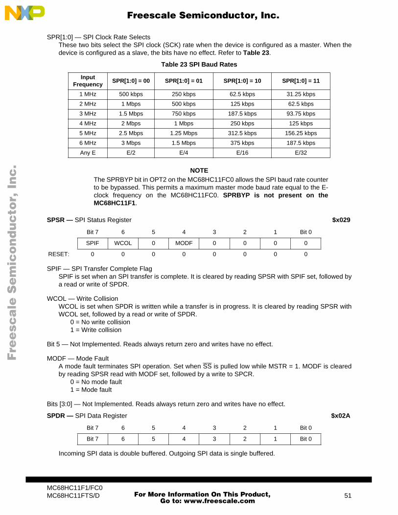
F
ree
sca
le S
em
ico
nd
uc
tor,
I
Freescale Semiconductor, Inc.n
c..
.
SPR[1:0] — SPI Clock Rate SelectsThese two bits select the SPI clock (SCK) rate when the device is configured as a master. When thedevice is configured as a slave, the bits have no effect. Refer to Table 23.
NOTEThe SPRBYP bit in OPT2 on the MC68HC11FC0 allows the SPI baud rate counterto be bypassed. This permits a maximum master mode baud rate equal to the E-clock frequency on the MC68HC11FC0. SPRBYP is not present on theMC68HC11F1.
SPIF — SPI Transfer Complete FlagSPIF is set when an SPI transfer is complete. It is cleared by reading SPSR with SPIF set, followed bya read or write of SPDR.
WCOL — Write CollisionWCOL is set when SPDR is written while a transfer is in progress. It is cleared by reading SPSR withWCOL set, followed by a read or write of SPDR.
0 = No write collision1 = Write collision
Bit 5 — Not Implemented. Reads always return zero and writes have no effect.
MODF — Mode Fault A mode fault terminates SPI operation. Set when SS is pulled low while MSTR = 1. MODF is clearedby reading SPSR read with MODF set, followed by a write to SPCR.
0 = No mode fault1 = Mode fault
Bits [3:0] — Not Implemented. Reads always return zero and writes have no effect.
Incoming SPI data is double buffered. Outgoing SPI data is single buffered.
Table 23 SPI Baud Rates
Input Frequency
SPR[1:0] = 00 SPR[1:0] = 01 SPR[1:0] = 10 SPR[1:0] = 11
1 MHz 500 kbps 250 kbps 62.5 kbps 31.25 kbps
2 MHz 1 Mbps 500 kbps 125 kbps 62.5 kbps
3 MHz 1.5 Mbps 750 kbps 187.5 kbps 93.75 kbps
4 MHz 2 Mbps 1 Mbps 250 kbps 125 kbps
5 MHz 2.5 Mbps 1.25 Mbps 312.5 kbps 156.25 kbps
6 MHz 3 Mbps 1.5 Mbps 375 kbps 187.5 kbps
Any E E/2 E/4 E/16 E/32
SPSR — SPI Status Register $x029
Bit 7 6 5 4 3 2 1 Bit 0
SPIF WCOL 0 MODF 0 0 0 0
RESET: 0 0 0 0 0 0 0 0
SPDR — SPI Data Register $x02A
Bit 7 6 5 4 3 2 1 Bit 0
Bit 7 6 5 4 3 2 1 Bit 0
MC68HC11F1/FC0 MC68HC11FTS/D 51
For More Information On This Product,
Go to: www.freescale.com
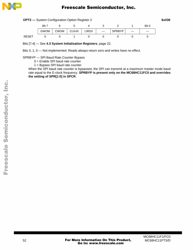
F
ree
sca
le S
em
ico
nd
uc
tor,
I
Freescale Semiconductor, Inc.n
c..
.
Bits [7:4] — See 4.3 System Initialization Registers, page 22.
Bits 3, 1, 0 — Not implemented. Reads always return zero and writes have no effect.
SPRBYP — SPI Baud Rate Counter Bypass0 = Enable SPI baud rate counter1 = Bypass SPI baud rate counter
When the SPI baud rate counter is bypassed, the SPI can transmit at a maximum master mode baudrate equal to the E-clock frequency. SPRBYP is present only on the MC68HC11FC0 and overridesthe setting of SPR[1:0] in SPCR.
OPT2 — System Configuration Option Register 2 $x038
Bit 7 6 5 4 3 2 1 Bit 0
GWOM CWOM CLK4X LIRDV — SPRBYP — —
RESET 0 0 1 0 0 0 0 0
MC68HC11F1/FC052 MC68HC11FTS/D
For More Information On This Product,
Go to: www.freescale.com

F
ree
sca
le S
em
ico
nd
uc
tor,
I
Freescale Semiconductor, Inc.n
c..
.
11 Analog-to-Digital ConverterThe MC68HC11F1 analog-to-digital (A/D) converter system uses an all-capacitive charge-redistributiontechnique to convert analog signals to digital values. The A/D system is an 8-channel, 8-bit, multiplexed-input, successive-approximation converter, accurate to ±1 least significant bit (LSB). Because the ca-pacitive charge redistribution technique used includes a built-in sample-and-hold, no external sample-and-hold is required.
Dedicated lines VRH and VRL provide the reference supply voltage inputs. Systems operating at clockrates of 750 kHz or below must use an internal RC oscillator. The CSEL bit in the OPTION register se-lects the clock source for the A/D system. (The CSEL bit is described in 11.3 A/D Registers, page 56.)
A multiplexer allows the single A/D converter to select one of 16 analog signals, as shown in Table 24.
NOTEThe A/D converter is present on the MC68HC11F1 only.
Figure 14 A/D Converter Block Diagram
EA9 A/D BLOCK
PE0AN0
PE1AN1
PE2AN2
PE3AN3
PE4AN4
PE5AN5
PE6AN6
PE7AN7
ANALOGMUX
8-BIT CAPACITIVE DACWITH SAMPLE AND HOLD
SUCCESSIVE APPROXIMATIONREGISTER AND CONTROL
ADCTL A/D CONTROL
CB
CC
CD
MU
LT
SCAN
CC
F
CA
ADR1 A/D RESULT 1 ADR2 A/D RESULT 2 ADR3 A/D RESULT 3 ADR4 A/D RESULT 4
RESULT REGISTER INTERFACE
RESULT
INTERNALDATA BUS
VRH
VRL
MC68HC11F1/FC0 MC68HC11FTS/D 53
For More Information On This Product,
Go to: www.freescale.com

F
ree
sca
le S
em
ico
nd
uc
tor,
I
Freescale Semiconductor, Inc.n
c..
.
11.1 Input Pins
Port E pins can also be used as digital inputs. Reads of port E pins are not recommended during thesample portion of an A/D conversion cycle, when the gate signal to the N-channel input gate is on. Be-cause no P-channel devices are directly connected to either input pins or reference voltage pins, volt-ages above VDD do not cause a latchup problem, although current should be limited according tomaximum ratings. Figure 15 is a functional diagram of an input pin.
Figure 15 Electrical Model of an Analog Input Pin (Sample Mode)
11.2 Conversion Sequence
A/D converter operations are performed in sequences of four conversions each. A conversion sequencecan be repeated continuously or stop after one iteration. The conversion complete flag (CCF) is set afterthe fourth conversion in a sequence to show the availability of data in the result registers. Figure 16shows the timing of a typical sequence. Synchronization is referenced to the system E clock.
Figure 16 A/D Conversion Sequence
DIFFUSION/POLY
< 2 pF
COUPLER
400 nAJUNCTIONLEAKAGE
+ ~20V– ~0.7V
*
* THIS ANALOG SWITCH IS CLOSED ONLY DURING THE 12-CYCLE SAMPLE TIME.
VRL
INPUT
+ ~12V– ~0.7V
PROTECTIONDEVICE
≤ 4 KΩ
DUMMY N-CHANNELOUTPUT DEVICE
ANALOGINPUT
PIN
~ 20 pFDAC
CAPACITANCE
0 32 64 96 128 — E CYCLES
SAMPLE ANALOG INPUT SUCCESSIVE APPROXIMATION SEQUENCE
MSB4
CYCLES
BIT 62
CYC
BIT 52
CYC
BIT 42
CYC
BIT 32
CYC
BIT 22
CYC
BIT 12
CYC
LSB2
CYC
2CYCEND
REP
EAT
SEQ
UEN
CE,
SC
AN =
1
SET
CC
FLA
G
CONVERT FIRSTCHANNEL, UPDATE
ADR1
CONVERT SECONDCHANNEL, UPDATE
ADR2
CONVERT THIRDCHANNEL, UPDATE
ADR3
CONVERT FOURTHCHANNEL, UPDATE
ADR4
12 E CYCLES
WR
ITE
TO A
DC
TL
E CLOCK
MC68HC11F1/FC054 MC68HC11FTS/D
For More Information On This Product,
Go to: www.freescale.com
F
ree
sca
le S
em
ico
nd
uc
tor,
I
Freescale Semiconductor, Inc.n
c..
.
11.3 A/D Registers
I = Indeterminate value
CCF — Conversions Complete FlagA read-only status indicator, this bit is set when all four A/D result registers contain valid conversion re-sults. Each time the ADCTL register is overwritten, this bit is automatically cleared to zero and a con-version sequence is started. In the continuous mode, CCF is set at the end of the first conversionsequence.
Bit 6 — Not implemented. Reads always return zero and writes have no effect.
SCAN — Continuous Scan Control0 = Do four conversions and stop1 = Convert four channels in selected group continuously
MULT — Multiple Channel/Single Channel Control0 = Convert single channel selected1 = Convert four channels in selected group
CD–CA — Channel Select D through ARefer to Table 24. When a multiple channel mode is selected (MULT = 1), the two least significant chan-nel select bits (CB and CA) have no meaning and the CD and CC bits specify which group of four chan-nels is to be converted.
NOTES:1. Used for factory testing.
ADCTL — A/D Control/Status $x030
Bit 7 6 5 4 3 2 1 Bit 0
CCF 0 SCAN MULT CD CC CB CA
RESET: I 0 I I I I I I
Table 24 A/D Converter Channel Assignments
Channel Select Control BitsCD:CC:CB:CA
Channel Signal Result in ADRx if MULT = 1
0000 AN0 ADR1
0001 AN1 ADR2
0010 AN2 ADR3
0011 AN3 ADR4
0100 AN4 ADR1
0101 AN5 ADR2
0110 AN6 ADR3
0111 AN7 ADR4
10XX Reserved ADR1–ADR4
1100 VRH1 ADR1
1101 VRL1 ADR2
1110 (VRH)/21 ADR3
1111 Reserved1 ADR4
MC68HC11F1/FC0 MC68HC11FTS/D 55
For More Information On This Product,
Go to: www.freescale.com

F
ree
sca
le S
em
ico
nd
uc
tor,
I
Freescale Semiconductor, Inc.n
c..
.
Each read-only result register holds an eight-bit conversion result. Writes to these registers have no ef-fect. Data in the A/D converter result registers is valid when the CCF flag in the ADCTL register is set,indicating a conversion sequence is complete. If conversion results are needed sooner, refer to Figure16, which shows the A/D conversion sequence diagram.
*Can be written only once in first 64 cycles out of reset in normal modes, or at any time in special modes.
ADPU — A/D Power Up0 = A/D powered down1 = A/D powered up
CSEL — Clock Select 0 = A/D and EEPROM use system E-Clock1 = A/D and EEPROM use internal RC clock
Bits [5:0] — Refer to 4.3 System Initialization Registers, page 23.
NOTES:1. % of VRH–VRL2. Volts for VRL = 0; VRH = 5.0 V
ADR1 – ADR4 — A/D Results $x031 – $x034
$x031 Bit 7 6 5 4 3 2 1 Bit 0 ADR1
$x032 Bit 7 6 5 4 3 2 1 Bit 0 ADR2
$x033 Bit 7 6 5 4 3 2 1 Bit 0 ADR3
$x034 Bit 7 6 5 4 3 2 1 Bit 0 ADR4
Table 25 Analog Input to 8-Bit Result Translation Table
Bit 7 6 5 4 3 2 1 Bit 0
Percentage1 50% 25% 12.5% 6.25% 3.12% 1.56% 0.78% 0.39%
Volts2 2.500 1.250 0.625 0.3125 0.1562 0.0781 0.0391 0.0195
OPTION — System Configuration Options $x039
Bit 7 6 5 4 3 2 1 Bit 0
ADPU CSEL IRQE* DLY* CME FCME* CR1* CR0*
RESET: 0 0 0 1 0 0 0 0
MC68HC11F1/FC056 MC68HC11FTS/D
For More Information On This Product,
Go to: www.freescale.com

F
ree
sca
le S
em
ico
nd
uc
tor,
I
Freescale Semiconductor, Inc.n
c..
.
12 Main TimerThe main timer is based on a free-running 16-bit counter with a four-stage programmable prescaler. Thetimer drives the three input capture (IC) channels, four output compare (OC) channels, one channel pro-grammable for either IC or OC, and the pulse accumulator (PA). All of these functions share port A. Themain timer also drives the pulse accumulator, real-time interrupt (RTI), and computer operating properly(COP) watchdog circuits.
12.1 Timer Operation
The following tables summarize timing periods for various M68HC11 functions derived from the maintimer for several crystal frequencies.
Table 26 Timer Subsystem Count and Overflow Periods
E-Clock Frequency
PR[1:0] = 00 PR[1:0] = 01 PR[1:0] = 10 PR[1:0] = 11
1 CountTCNT
Overflow1 Count
TCNT Overflow
1 CountTCNT
Overflow1 Count
TCNT Overflow
1 MHz 1.000 µs 65.536 ms 4.000 µs 262.144 ms 8.000 µs 524.288 ms 16.000 µs 1.049 s
2 MHz 0.500 µs 32.768 ms 2.000 µs 131.072 ms 4.000 µs 262.144 ms 8.000 µs 524.288 ms
3 MHz 0.333 µs 21.845 ms 1.333 µs 87.381 ms 2.667 µs 174.763 ms 5.333 µs 349.525 ms
4 MHz 0.250 µs 16.384 ms 1.000 µs 65.536 ms 2.000 µs 131.072 ms 4.000 µs 262.144 ms
5 MHz 0.200 µs 13.107 ms 0.800 µs 52.429 ms 1.600 µs 104.858 ms 3.200 µs 209.715 ms
6 MHz 0.167 µs 10.923 ms 0.667 µs 43.691 ms 1.333 µs 87.381 ms 2.667 µs 174.763 ms
Any E 1/E 216/E 4/E 218/E 8/E 219/E 16/E 220/E
Table 27 Real-Time Interrupt Periods
E-Clock Frequency
RTR[1:0] = 00 RTR[1:0] = 01 RTR[1:0] = 10 RTR[1:0] = 11
1 MHz 8.192 ms 16.384 ms 32.768 ms 65.536 ms
2 MHz 4.096 ms 8.192 ms 16.384 ms 32.768 ms
3 MHz 2.731 ms 5.461 ms 10.923 ms 21.845 ms
4 MHz 2.048 ms 4.096 ms 8.192 ms 16.384 ms
5 MHz 1.638 ms 3.277 ms 6.554 ms 13.107 ms
6 MHz 1.366 ms 2.731 ms 5.461 ms 10.923 ms
Any E 213/E 214/E 215/E 221/E
Table 28 COP Watchdog Time-Out Periods
E-Clock Frequency
RTR[1:0] = 00 RTR[1:0] = 01 RTR[1:0] = 10 RTR[1:0] = 11
1 MHz 32.768 ms 131.072 ms 524.288 ms 2.097 s
2 MHz 16.384 ms 65.536 ms 262.144 ms 1.049 s
3 MHz 10.923 ms 43.691 ms 174.763 ms 699.051 ms
4 MHz 8.192 ms 32.768 ms 131.072 ms 524.288 ms
5 MHz 6.554 ms 26.214 ms 104.858 ms 419.430 ms
6 MHz 5.461 ms 21.845 ms 87.381 ms 349.525 ms
Any E 215/E 217/E 219/E 221/E
MC68HC11F1/FC0 MC68HC11FTS/D 57
For More Information On This Product,
Go to: www.freescale.com

F
ree
sca
le S
em
ico
nd
uc
tor,
I
Freescale Semiconductor, Inc.n
c..
.
Figure 17 Main Timer
IC/OC BLOCK
16-BIT LATCH CLK
Port APinTFLG 1
StatusFlags
OC1F
PA3
PA4
PA5
PA6
PA7
I4/O5
16-BIT COMPARATOR =
TOC1 (LO)
16-BIT FREE RUNNINGCOUNTER
TCNT (HI) TCNT (LO) TOI
PR1
16-BIT TIMER BUS
OC5
IC4
TMSK 1InterruptEnables
CFORC
PA0
PA1
PA2
IC3
IC2
IC1
PR0
E CLOCK
OC1
OC2/OC1
OC3/OC1
OC4/OC1
IC4/OC5OC1
TOF
8
FOC1TOC1 (HI)
OC3I
OC4I
I4O5I
7
6
5
4
FOC2
FOC3
FOC4
FOC5
16-BIT COMPARATOR =
TOC2 (LO)TOC2 (HI)
16-BIT COMPARATOR =
TOC3 (LO)TOC3 (HI)
16-BIT COMPARATOR =
TOC4 (LO)TOC4 (HI)
16-BIT COMPARATOR =
TI4O5 (LO)TI4O5 (HI)
3
2
1
IC1I
IC2I
IC3I
OC1I
OC2I
OC2F
OC3F
OC4F
I4O5F
IC1F
TIC1 (LO)TIC1 (HI)
IC2F
IC3F
TIC2 (LO)TIC2 (HI)
TIC3 (LO)TIC3 (HI)
9PRESCALER
Divide by1, 4, 8 or 16
InterruptRequests
Bit 7
Bit 6
Bit 5
Bit 4
Bit 3
Bit 2
Bit 1
Bit 0
Control(Note 1)
16-BIT LATCH CLK
16-BIT LATCH CLK
16-BIT LATCH CLK
To PulseAccumulator
PORT APins
NOTE: Registers that control port A action include DDRA, OC1M, OC1D, PACTL, TCTL1 and TCTL2.
MC68HC11F1/FC058 MC68HC11FTS/D
For More Information On This Product,
Go to: www.freescale.com

F
ree
sca
le S
em
ico
nd
uc
tor,
I
Freescale Semiconductor, Inc.n
c..
.
12.2 Timer Registers
FOCx — Force Output Compare x Action0 = Not affected1 = Output compare x action occurs, but OCxF flag bit is not set
Bits [2:0] — Not implemented. Reads always return zero and writes have no effect.
Bits set in OC1M allow OC1 to output the corresponding OC1D bits in port A when a successful com-pare event occurs.
OC1M[7:3] — Output Compare Masks0 = Control of the corresponding port A pin is disabled1 = Control of the corresponding port A pin is enabled
Bits [2:0] — Not implemented. Reads always return zero and writes have no effect.
OC1D[7:3] — Output Compare DataData in OC1Dx is output to port A bit x on successful OC1 compares if OC1Mx is set.
Bits [2:0] — Not implemented. Reads always return zero and writes have no effect.
The 16-bit read-only TCNT register contains the prescaled value of the 16-bit timer. A full counter readaddresses the most significant byte (MSB) first. A read of this address causes the least significant byteto be latched into a buffer for the next CPU cycle so that a double-byte read returns the full 16-bit stateof the counter at the time of the MSB read cycle.
CFORC — Timer Force Compare $x00B
Bit 7 6 5 4 3 2 1 Bit 0
FOC1 FOC2 FOC3 FOC4 FOC5 0 0 0
RESET: 0 0 0 0 0 0 0 0
OC1M — Output Compare 1 Mask $x00C
Bit 7 6 5 4 3 2 1 Bit 0
OC1M7 OC1M6 OC1M5 OC1M4 OC1M3 0 0 0
RESET: 0 0 0 0 0 0 0 0
OC1D — Output Compare 1 Data $x00D
Bit 7 6 5 4 3 2 1 Bit 0
OC1D7 OC1D6 OC1D5 OC1D4 OC1D3 0 0 0
RESET: 0 0 0 0 0 0 0 0
TCNT — Timer Count $x00E, $x00F
$x00E Bit 15 14 13 12 11 10 9 Bit 8 High
$x00F Bit 7 6 5 4 3 2 1 Bit 0 Low
RESET: 0 0 0 0 0 0 0 0
MC68HC11F1/FC0 MC68HC11FTS/D 59
For More Information On This Product,
Go to: www.freescale.com

F
ree
sca
le S
em
ico
nd
uc
tor,
I
Freescale Semiconductor, Inc.n
c..
.
TICx registers are not affected by reset.
All TOCx register pairs are reset to ones ($FFFF).
TI4/O5 is reset to ones ($FFFF).
OM2–OM5 — Output Mode
OL2–OL5 — Output LevelEach OMx–OLx bit pair determines the output action taken on the corresponding OCx pin after a suc-cessful compare, as shown in Table 29. OC5 functions only if the I4/O5 bit in the PACTL register iscleared.
TIC1–TIC3 — Timer Input Capture $x010–$x015
$x010 Bit 15 14 13 12 11 10 9 Bit 8 High
$x011 Bit 7 6 5 4 3 2 1 Bit 0 Low
$x012 Bit 15 14 13 12 11 10 9 Bit 8 High
$x013 Bit 7 6 5 4 3 2 1 Bit 0 Low
$x014 Bit 15 14 13 12 11 10 9 Bit 8 High
$x015 Bit 7 6 5 4 3 2 1 Bit 0 Low
TOC1–TOC4 — Timer Output Compare $x016–$x01D
$x016 Bit 15 14 13 12 11 10 9 Bit 8 High
$x017 Bit 7 6 5 4 3 2 1 Bit 0 Low
$x018 Bit 15 14 13 12 11 10 9 Bit 8 High
$x019 Bit 7 6 5 4 3 2 1 Bit 0 Low
$x01A Bit 15 14 13 12 11 10 9 Bit 8 High
$x01B Bit 7 6 5 4 3 2 1 Bit 0 Low
$x01C Bit 15 14 13 12 11 10 9 Bit 8 High
$x01D Bit 7 6 5 4 3 2 1 Bit 0 Low
TI4/O5 — Timer Input Capture 4/Output Compare 5 $x01E, $x01F
$x01E Bit 15 14 13 12 11 10 9 Bit 8 High
$x01F Bit 7 6 5 4 3 2 1 Bit 0 Low
TCTL1 — Timer Control 1 $x020
Bit 7 6 5 4 3 2 1 Bit 0
OM2 OL2 OM3 OL3 OM4 OL4 OM5 OL5
RESET: 0 0 0 0 0 0 0 0
MC68HC11F1/FC060 MC68HC11FTS/D
For More Information On This Product,
Go to: www.freescale.com
F
ree
sca
le S
em
ico
nd
uc
tor,
I
Freescale Semiconductor, Inc.n
c..
.
EDGxB, EDGxA — Input Capture Edge ControlEach EDGxB, EDGxA pair determines the polarity of the input signal on the corresponding ICx that willtrigger an input capture, as shown in Table 30. IC4 functions only if the I4/O5 bit in the PACTL registeris set.
Bits in TMSK1 correspond bit for bit with flag bits in TFLG1. Each bit that is set in TMSK1 enables thecorresponding interrupt source.
OCxI — Output Compare x Interrupt EnableIf the OCxI enable bit is set when the OCxF flag bit is set, a hardware interrupt sequence is requested.
I4/O5I — Input Capture 4/Output Compare 5 Interrupt EnableWhen I4/O5 in PACTL is one, I4/O5I is the input capture 4 interrupt enable bit. When I4/O5 in PACTLis zero, I4/O5I is the output compare 5 interrupt enable bit.
ICxI — Input Capture x Interrupt EnableIf the ICxI enable bit is set when the ICxF flag bit is set, a hardware interrupt sequence is requested.
Bits in TFLG1 are cleared by writing a one to the corresponding bit positions.
Table 29 Output Compare Actions
OMx OLx Action Taken on Successful Compare
0 0 Timer disconnected from output pin logic
0 1 Toggle OCx output line
1 0 Clear OCx output line to zero
1 1 Set OCx output line to one
TCTL2 — Timer Control 2 $x021
Bit 7 6 5 4 3 2 1 Bit 0
EDG4B EDG4A EDG1B EDG1A EDG2B EDG2A EDG3B EDG3A
RESET: 0 0 0 0 0 0 0 0
Table 30 Input Capture Configuration
EDGxB EDGxA Configuration
0 0 Capture disabled
0 1 Capture on rising edges only
1 0 Capture on falling edges only
1 1 Capture on any edge
TMSK1 — Timer Interrupt Mask 1 $x022
Bit 7 6 5 4 3 2 1 Bit 0
OC1I OC2I OC3I OC4I I4/O5I IC1I IC2I IC3I
RESET: 0 0 0 0 0 0 0 0
TFLG1 — Timer Interrupt Flag 1 $x023
Bit 7 6 5 4 3 2 1 Bit 0
OC1F OC2F OC3F OC4F I4/O5F IC1F IC2F IC3F
RESET: 0 0 0 0 0 0 0 0
MC68HC11F1/FC0 MC68HC11FTS/D 61
For More Information On This Product,
Go to: www.freescale.com

F
ree
sca
le S
em
ico
nd
uc
tor,
I
Freescale Semiconductor, Inc.n
c..
.
OCxF — Output Compare x FlagSet each time the counter matches output compare x value.
I4/O5F — Input Capture 4/Output Compare 5 FlagSet by IC4 or OC5, depending on which function was enabled by I4/O5 of PACTL.
ICxF — Input Capture x FlagSet each time a selected active edge is detected on the ICx input line.
Bits [7:4] in TMSK2 correspond bit for bit with flag bits in TFLG2. Setting any of these bits enables thecorresponding interrupt source. TMSK2 can be written only once in the first 64 cycles out of reset innormal modes, or at any time in special modes.
TOI — Timer Overflow Interrupt Enable0 = Timer overflow interrupt disabled1 = Interrupt requested when TOF is set
RTII — Real-Time Interrupt Enable0 = Real-time interrupt disabled1 = Interrupt requested when RTIF is set
Bits [5:4] — See 13.2 Pulse Accumulator Registers, page 64.
Bits [3:2] — Not implemented. Reads always return zero and writes have no effect.
PR[1:0] — Timer Prescaler SelectDetermines the main timer prescale factor as shown in Table 31. See Table 26 for specific frequencies.
Bits in this register indicate when certain timer system events have occurred. Coupled with the fourhigh-order bits of TMSK2, the bits of TFLG2 allow the timer subsystem to operate in either a polled orinterrupt driven system. Each bit of TFLG2 corresponds to a bit in TMSK2 in the same position.
Bits in TFLG2 are cleared by writing a one to the corresponding bit positions.
TOF — Timer Overflow FlagSet when TCNT rolls over from $FFFF to $0000.
TMSK2 — Timer Interrupt Mask 2 $x024
Bit 7 6 5 4 3 2 1 Bit 0
TOI RTII PAOVI PAII 0 0 PR1 PR0
RESET: 0 0 0 0 0 0 0 0
Table 31 Main Timer Prescale Control
PR[1:0] Prescaler
0 0 1
0 1 4
1 0 8
1 1 16
TFLG2 — Timer Interrupt Flag 2 $x025
Bit 7 6 5 4 3 2 1 Bit 0
TOF RTIF PAOVF PAIF 0 0 0 0
RESET: 0 0 0 0 0 0 0 0
MC68HC11F1/FC062 MC68HC11FTS/D
For More Information On This Product,
Go to: www.freescale.com

F
ree
sca
le S
em
ico
nd
uc
tor,
I
Freescale Semiconductor, Inc.n
c..
.
RTIF — Real-Time Interrupt FlagSet periodically at a rate based on bits RTR[1:0] in the PACTL register.
Bits [5:4] — See 13.2 Pulse Accumulator Registers, page 65.
Bits [3:0] — Not implemented. Reads always return zero and writes have no effect.
Bit 7 — Not implemented. Reads always return zero and writes have no effect.
Bits [6:4] — See 13.2 Pulse Accumulator Registers, page 65.
Bit 3 — Not implemented. Reads always return zero and writes have no effect.
I4/O5 — Configure TI4/O5 Register for IC or OC0 = OC5 function enabled1 = IC4 function enabled
RTR[1:0] — RTI Interrupt Rate SelectsThese two bits select one of four rates for the real-time interrupt circuit, as shown in Table 32.
PACTL — Pulse Accumulator Control $x026
Bit 7 6 5 4 3 2 1 Bit 0
0 PAEN PAMOD PEDGE 0 I4/O5 RTR1 RTR0
RESET: 0 0 0 0 0 0 0 0
Table 32 Real-Time Interrupt Periods
E-Clock Frequency
RTR [1:0] = %00 RTR [1:0] = 01 RTR [1:0] = 10 RTR [1:0] = 11
1 MHz 8.192 ms 16.384 ms 32.768 ms 65.536 ms
2 MHz 4.906 ms 8.192 ms 16.384 ms 32.768 ms
3 MHz 2.731 ms 5.461 ms 10.923 ms 21.845 ms
4 MHz 2.048 ms 4.096 ms 8.192 ms 16.384 ms
5 MHz 1.638 ms 3.277 ms 6.554 ms 13.107 ms
6 MHz 1.366 ms 2.731 ms 5.461 ms 10.923 ms
Any E 213/E 214/E 215/E 216/E
MC68HC11F1/FC0 MC68HC11FTS/D 63
For More Information On This Product,
Go to: www.freescale.com

F
ree
sca
le S
em
ico
nd
uc
tor,
I
Freescale Semiconductor, Inc.n
c..
.
13 Pulse AccumulatorThe pulse accumulator can be used either to count events or measure the duration of a particular event.In event counting mode, the pulse accumulator’s 8-bit counter increments each time a specified edgeis detected on the pulse accumulator input pin, PA7. The maximum clocking rate for this mode is the E-clock divided by two. In gated time accumulation mode, an internal clock increments the 8-bit counterat a rate of E-clock ÷ 64 while the input at PA7 remains at a predetermined logic level.
13.1 Pulse Accumulator Block Diagram
Figure 18 Pulse Accumulator Block Diagram
13.2 Pulse Accumulator Registers
Bits [7:4] in TMSK2 correspond bit for bit with flag bits in TFLG2. Setting any of these bits enables thecorresponding interrupt source.
TMSK2 — Timer Interrupt Mask 2 $x024
Bit 7 6 5 4 3 2 1 Bit 0
TOI RTII PAOVI PAII 0 0 PR1 PR0
RESET: 0 0 0 0 0 0 0 0
PACNT 8-BIT COUNTER
2:1MUX
PA7/
ENABLE
OVERFLOW
1
INTERRUPTREQUESTS
INTERNAL DATA BUS
INPUT BUFFER&
EDGE DETECTION
PACTL
TFLG2TMSK2PA
OVI
PAII
PAEN
PAM
OD
PED
GE
PAO
VF
PAIF
OUTPUTBUFFER
PAI EDGE
PAEN
E ÷ 64 CLOCK(FROM MAIN TIMER)
PAI/OC1
FROMMAIN TIMER
OC1
PAEN
2
CLOCK
FROM
STATUS FLAGSINTERRUPT ENABLES
CONTROLDDRA
MC68HC11F1/FC064 MC68HC11FTS/D
For More Information On This Product,
Go to: www.freescale.com
F
ree
sca
le S
em
ico
nd
uc
tor,
I
Freescale Semiconductor, Inc.n
c..
.
Bits[7:6] — See 12.2 Timer Registers, page 62.
PAOVI — Pulse Accumulator Overflow Interrupt Enable0 = Pulse accumulator overflow interrupt disabled1 = Interrupt requested when PAOVF in TFLG2 is set
PAII — Pulse Accumulator Interrupt Enable0 = Pulse accumulator interrupt disabled1 = Interrupt requested when PAIF in TFLG2 is set
Bits [3:2] — Not implemented. Reads always return zero and writes have no effect.
Bits [1:0] — See 12.2 Timer Registers, page 62.
Bits in TFLG2 are cleared by writing a one to the corresponding bit positions.
Bits [7:6] — See 12.2 Timer Registers, page 62.
PAOVF — Pulse Accumulator Overflow FlagSet when PACNT rolls over from $FF to $00
PAIF — Pulse Accumulator Input Edge FlagSet each time a selected active edge is detected on the PAI input line
Bits [3:0] — Not implemented. Reads always return zero and writes have no effect.
Bit 7 — Not implemented. Reads always return zero and writes have no effect.
PAEN — Pulse Accumulator System Enable0 = Pulse accumulator disabled1 = Pulse accumulator enabled
PAMOD — Pulse Accumulator Mode0 = Event counter1 = Gated time accumulation
PEDGE — Pulse Accumulator Edge ControlThis bit has different meanings depending on the state of the PAMOD bit, as shown in Table 33.
TFLG2 — Timer Interrupt Flag 2 $x025
Bit 7 6 5 4 3 2 1 Bit 0
TOF RTIF PAOVF PAIF 0 0 0 0
RESET: 0 0 0 0 0 0 0 0
PACTL — Pulse Accumulator Control $x026
Bit 7 6 5 4 3 2 1 Bit 0
0 PAEN PAMOD PEDGE 0 I4/O5 RTR1 RTR0
RESET: 0 0 0 0 0 0 0 0
MC68HC11F1/FC0 MC68HC11FTS/D 65
For More Information On This Product,
Go to: www.freescale.com

F
ree
sca
le S
em
ico
nd
uc
tor,
I
Freescale Semiconductor, Inc.n
c..
.
Bit 3 — Not implemented. Reads always return zero and writes have no effect.
Bits [2:0] — See 12.2 Timer Registers, page 63.
U = Unaffected by reset
This eight-bit read/write register contains the count of external input events at the PAI input, or the ac-cumulated count. The PACNT is readable even if PAI is not active in gated time accumulation mode.The counter is not affected by reset and can be read or written at any time. Counting is synchronizedto the internal PH2 clock so that incrementing and reading occur during opposite half cycles.
Table 33 Pulse Accumulator Edge Control
PAMOD PEDGE Action on Clock
0 0 PAI falling edge increments the counter.
0 1 PAI rising edge increments the counter.
1 0 A zero on PAI inhibits counting.
1 1 A one on PAI inhibits counting.
PACNT — Pulse Accumulator Count $x027
Bit 7 6 5 4 3 2 1 Bit 0
Bit 7 6 5 4 3 2 1 Bit 0
RESET: U U U U U U U U
MC68HC11F1/FC066 MC68HC11FTS/D
For More Information On This Product,
Go to: www.freescale.com
F
ree
sca
le S
em
ico
nd
uc
tor,
I
Freescale Semiconductor, Inc.n
c..
.
MC68HC11F1/FC0 MC68HC11FTS/D 67
For More Information On This Product,
Go to: www.freescale.com

How to reach us:USA/EUROPE/Locations Not Listed: Motorola Literature Distribution; P.O. Box 5405, Denver Colorado 80217. 1-800-441-2447, (303) 675-2140Mfax™: [email protected] - TOUCHTONE (602) 244-6609INTERNET: http://Design-NET.comJAPAN: Nippon Motorola Ltd.; Tatsumi-SPD-JLDC, 6F Seibu-Butsuryu-Center, 3-14-2 Tatsumi Koto-Ku, Tokyo 135, Japan. 81-3-3521-8315ASIA PACIFIC: Motorola Semiconductors H.K. Ltd.; 8B Tai Ping Industrial Park, 51 Ting Kok Road, Tai Po, N.T., Hong Kong. 852-26629298Mfax is a trademark of Motorola, Inc.
Motorola reserves the right to make changes without further notice to any products herein. Motorola makes no warranty, representation or guarantee regarding the suitabilityof its products for any particular purpose, nor does Motorola assume any liability arising out of the application or use of any product or circuit, and specifically disclaims any andall liability, including without limitation consequential or incidental damages. "Typical" parameters which may be provided in Motorola data sheets and/or specifications can anddo vary in different applications. All operating parameters, including "Typicals" must be validated for each customer application by customer's technical experts. Motorola doesnot convey any license under its patent rights nor the rights of others. Motorola products are not designed, intended, or authorized for use as components in systems intendedfor surgical implant into the body, or other applications intended to support or sustain life, or for any other application in which the failure of the Motorola product could create asituation where personal injury or death may occur. Should Buyer purchase or use Motorola products for any such unintended or unauthorized application, Buyer shall indemnifyand hold Motorola and its officers, employees, subsidiaries, affiliates, and distributors harmless against all claims, costs, damages, and expenses, and reasonable attorney feesarising out of, directly or indirectly, any claim of personal injury or death associated with such unintended or unauthorized use, even if such claim alleges that Motorola wasnegligent regarding the design or manufacture of the part. MCUinit, MCUasm, MCUdebug, and RTEK are trademarks of Motorola, Inc. M O T O R O L A and ! are registered trademarks of Motorola, Inc. Motorola, Inc. is an EqualOpportunity/Affirmative Action Employer.
Fre
esc
ale
Se
mic
on
du
cto
r, I
Freescale Semiconductor, Inc.
For More Information On This Product, Go to: www.freescale.com
nc
...