Embed Size (px)
Citation preview
ASIC Design Methodology using Cadence SP&R Flow (Information about PKS-SE and ASIC design flow borrowed from Cadence documents.)
1 ASIC Design Methodology The tasks involved in ASIC design are usually split up into two sections: Front
End tasks and Back end tasks, as shown in the following diagram:
Figure 1. ASIC Design Stages
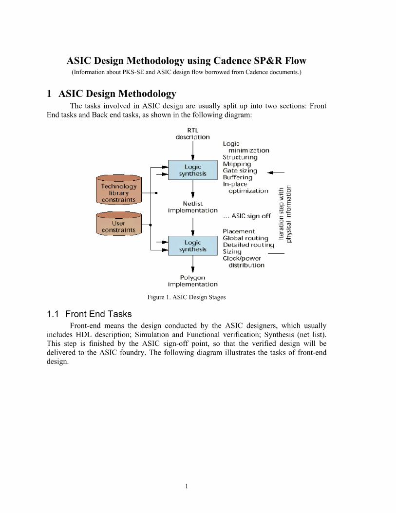
1.1 Front End Tasks Front-end means the design conducted by the ASIC designers, which usually
includes HDL description; Simulation and Functional verification; Synthesis (net list). This step is finished by the ASIC sign-off point, so that the verified design will be delivered to the ASIC foundry. The following diagram illustrates the tasks of front-end design.
1
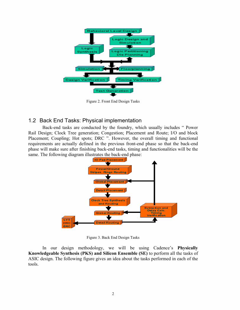
Figure 2. Front End Design Tasks
1.2 Back End Tasks: Physical implementation Back-end tasks are conducted by the foundry, which usually includes “ Power
Rail Design; Clock Tree generation; Congestion; Placement and Route; I/O and block Placement; Coupling; Hot spots; DRC ”. However, the overall timing and functional requirements are actually defined in the previous front-end phase so that the back-end phase will make sure after finishing back-end tasks, timing and functionalities will be the same. The following diagram illustrates the back-end phase:
Figure 3. Back End Design Tasks In our design methodology, we will be using Cadence’s Physically
Knowledgeable Synthesis (PKS) and Silicon Ensemble (SE) to perform all the tasks of ASIC design. The following figure gives an idea about the tasks performed in each of the tools.
2
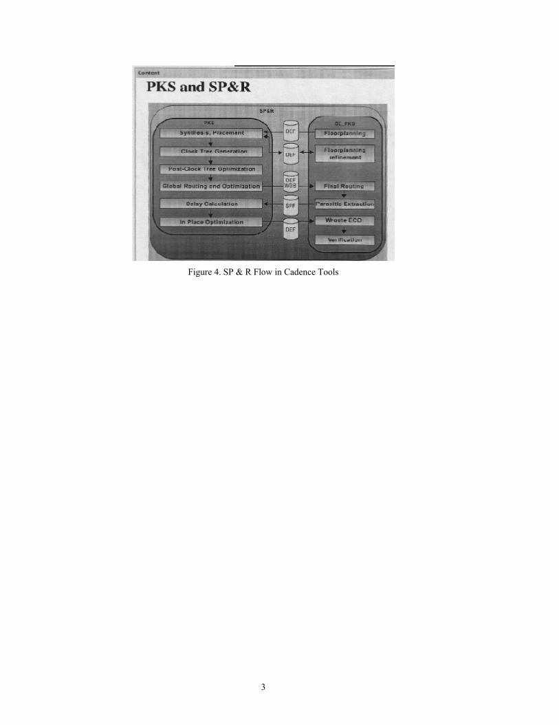
Figure 4. SP & R Flow in Cadence Tools
3
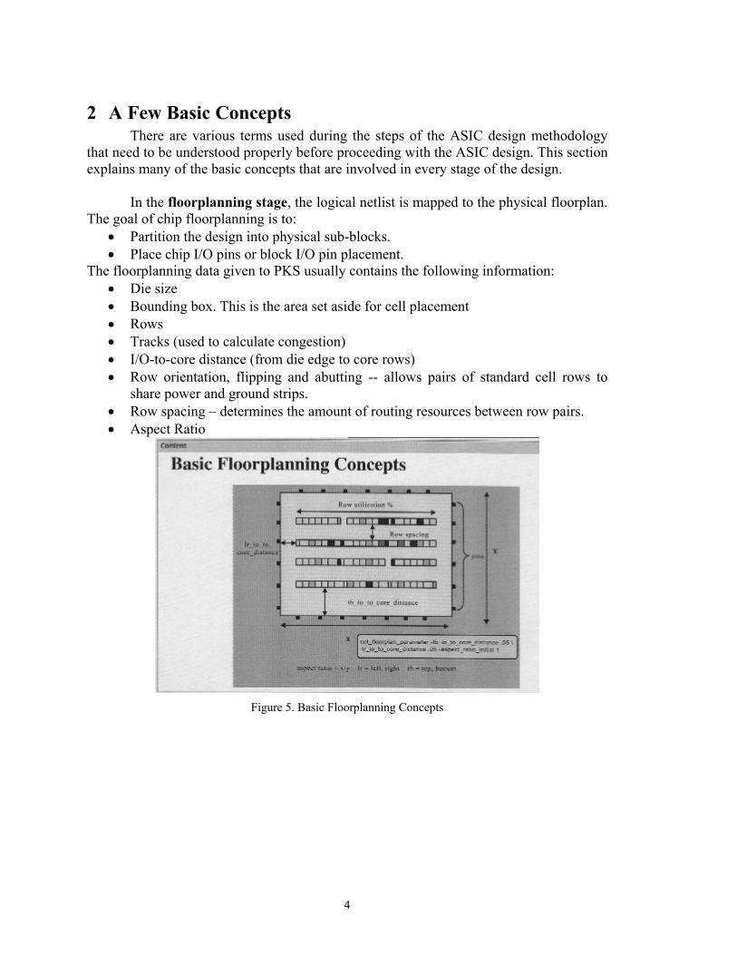
2 A Few Basic Concepts There are various terms used during the steps of the ASIC design methodology
that need to be understood properly before proceeding with the ASIC design. This section explains many of the basic concepts that are involved in every stage of the design.
In the floorplanning stage, the logical netlist is mapped to the physical floorplan. The goal of chip floorplanning is to:
• Partition the design into physical sub-blocks. • Place chip I/O pins or block I/O pin placement.
The floorplanning data given to PKS usually contains the following information: • Die size • Bounding box. This is the area set aside for cell placement • Rows • Tracks (used to calculate congestion) • I/O-to-core distance (from die edge to core rows) • Row orientation, flipping and abutting -- allows pairs of standard cell rows to
share power and ground strips. • Row spacing – determines the amount of routing resources between row pairs. • Aspect Ratio
Figure 5. Basic Floorplanning Concepts
4
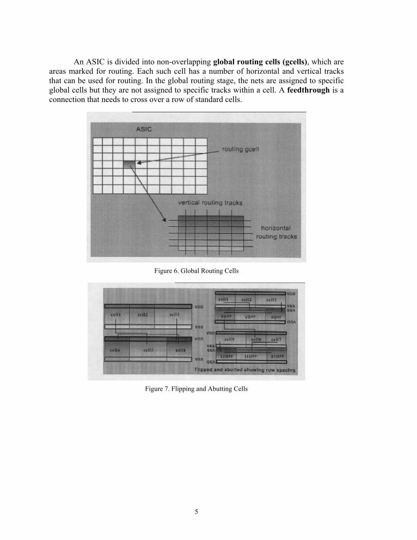
An ASIC is divided into non-overlapping global routing cells (gcells), which are
areas marked for routing. Each such cell has a number of horizontal and vertical tracks that can be used for routing. In the global routing stage, the nets are assigned to specific global cells but they are not assigned to specific tracks within a cell. A feedthrough is a connection that needs to cross over a row of standard cells.
Figure 6. Global Routing Cells
Figure 7. Flipping and Abutting Cells
5
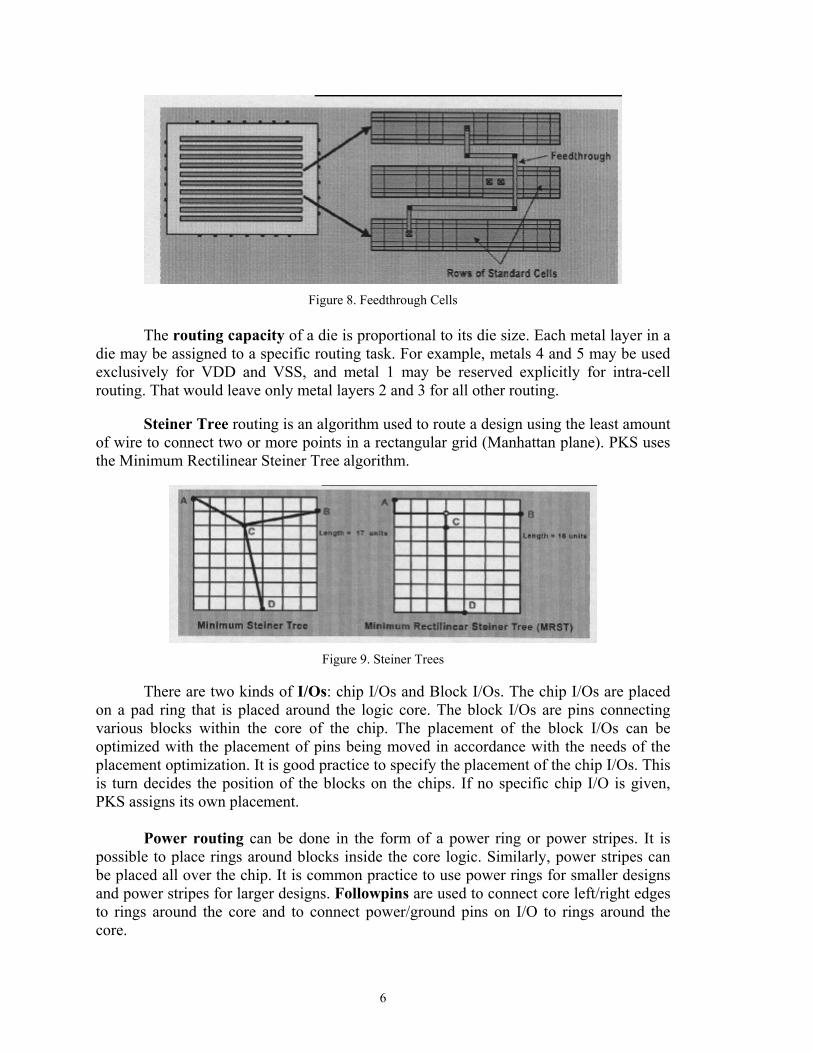
Figure 8. Feedthrough Cells
The routing capacity of a die is proportional to its die size. Each metal layer in a
die may be assigned to a specific routing task. For example, metals 4 and 5 may be used exclusively for VDD and VSS, and metal 1 may be reserved explicitly for intra-cell routing. That would leave only metal layers 2 and 3 for all other routing.
Steiner Tree routing is an algorithm used to route a design using the least amount of wire to connect two or more points in a rectangular grid (Manhattan plane). PKS uses the Minimum Rectilinear Steiner Tree algorithm.
Figure 9. Steiner Trees
There are two kinds of I/Os: chip I/Os and Block I/Os. The chip I/Os are placed
on a pad ring that is placed around the logic core. The block I/Os are pins connecting various blocks within the core of the chip. The placement of the block I/Os can be optimized with the placement of pins being moved in accordance with the needs of the placement optimization. It is good practice to specify the placement of the chip I/Os. This is turn decides the position of the blocks on the chips. If no specific chip I/O is given, PKS assigns its own placement.
Power routing can be done in the form of a power ring or power stripes. It is possible to place rings around blocks inside the core logic. Similarly, power stripes can be placed all over the chip. It is common practice to use power rings for smaller designs and power stripes for larger designs. Followpins are used to connect core left/right edges to rings around the core and to connect power/ground pins on I/O to rings around the core.
6
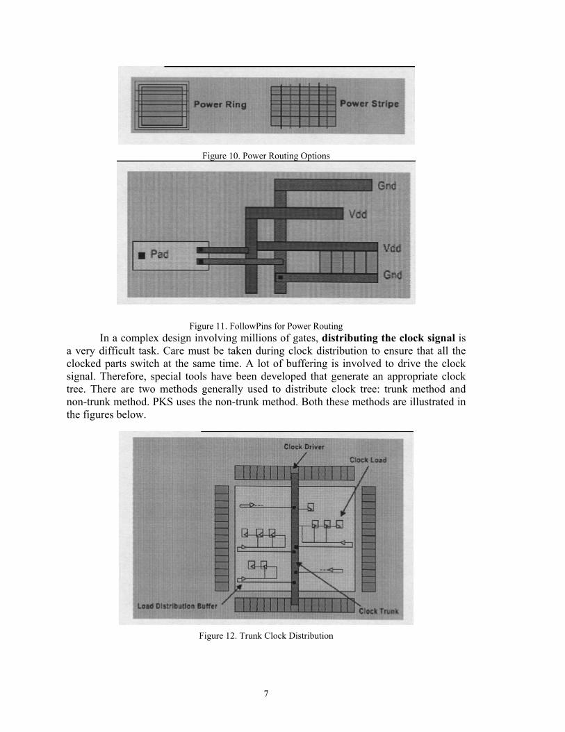
Figure 10. Power Routing Options
Figure 11. FollowPins for Power Routing In a complex design involving millions of gates, distributing the clock signal is
a very difficult task. Care must be taken during clock distribution to ensure that all the clocked parts switch at the same time. A lot of buffering is involved to drive the clock signal. Therefore, special tools have been developed that generate an appropriate clock tree. There are two methods generally used to distribute clock tree: trunk method and non-trunk method. PKS uses the non-trunk method. Both these methods are illustrated in the figures below.
Figure 12. Trunk Clock Distribution
7
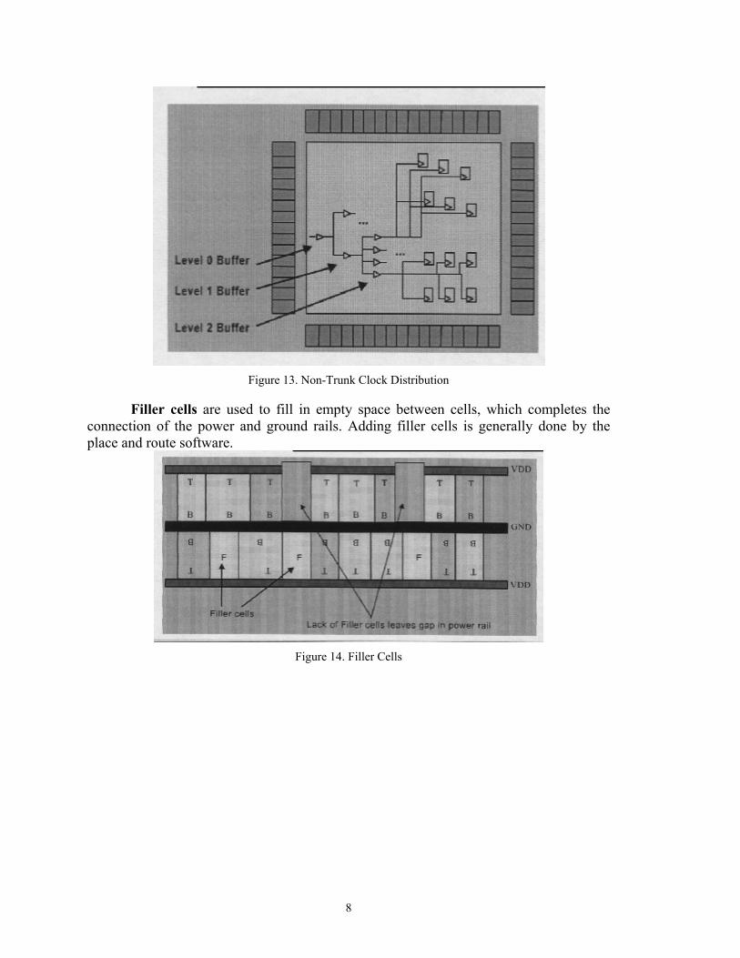
Figure 13. Non-Trunk Clock Distribution
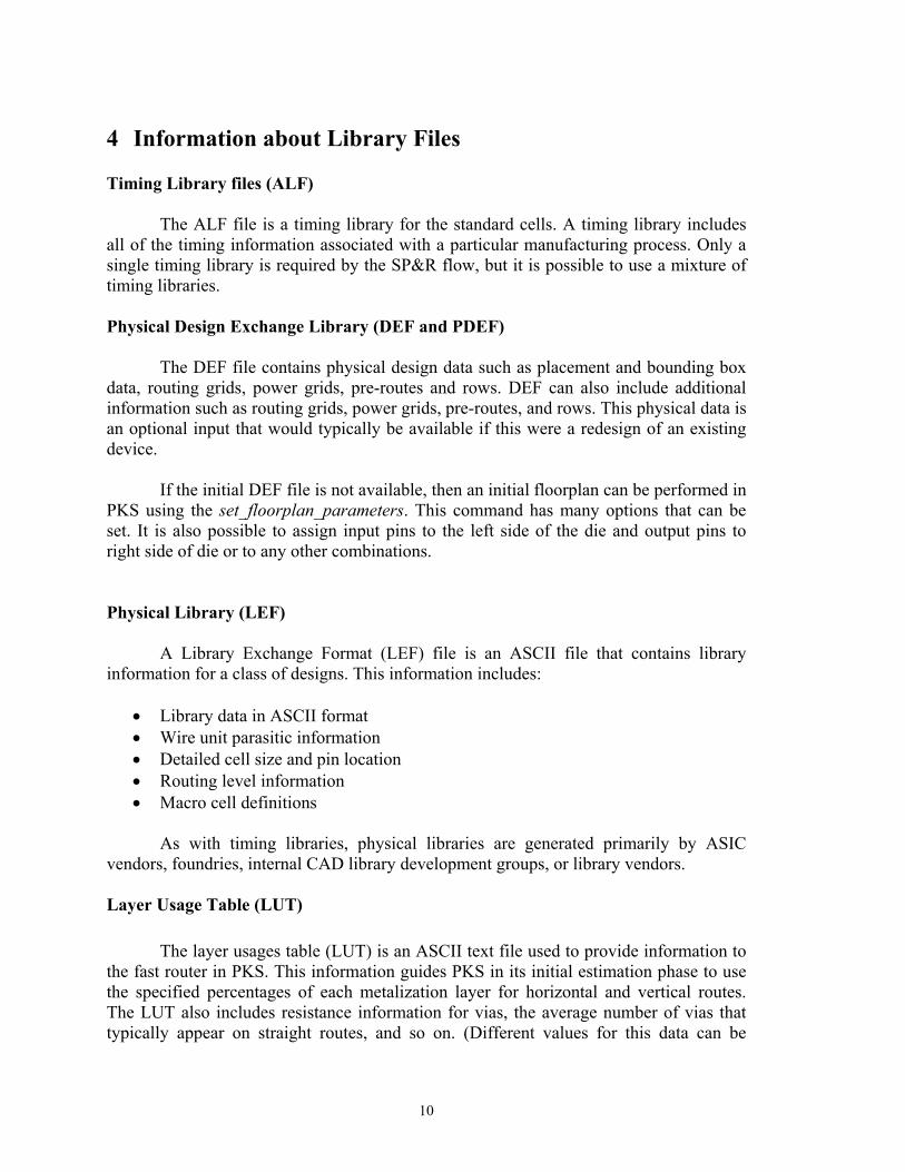
Filler cells are used to fill in empty space between cells, which completes the
connection of the power and ground rails. Adding filler cells is generally done by the place and route software.
Figure 14. Filler Cells
8

3 Commonly Used Acronyms • RTL: Register Transfer Level • ALF: Ambit Library Format • TLF: Timing Library Format • CTLF: Complied Timing Library Format • GCF: General Constraints Format • DEF: Design Exchange Format • PDEF: Physical Design Exchange Format • LEF: Library Exchange Format • ELEF: Encrypted Library Exchange Format • SDF: Standard Delay Format • WDB: WarpRoute Database • ADB: Ambit Database • SPF: Standard Parasitic Format • RSPF: Reduced Standard Parasitic Format • OLA: Open Library API • DCL: Delay Calculation Language • LDP: Logic Design Planner • PDP: Physical Design Planner
9
4 Information about Library Files Timing Library files (ALF)
The ALF file is a timing library for the standard cells. A timing library includes all of the timing information associated with a particular manufacturing process. Only a single timing library is required by the SP&R flow, but it is possible to use a mixture of timing libraries. Physical Design Exchange Library (DEF and PDEF)
The DEF file contains physical design data such as placement and bounding box data, routing grids, power grids, pre-routes and rows. DEF can also include additional information such as routing grids, power grids, pre-routes, and rows. This physical data is an optional input that would typically be available if this were a redesign of an existing device.
If the initial DEF file is not available, then an initial floorplan can be performed in PKS using the set_floorplan_parameters. This command has many options that can be set. It is also possible to assign input pins to the left side of the die and output pins to right side of die or to any other combinations. Physical Library (LEF)
A Library Exchange Format (LEF) file is an ASCII file that contains library information for a class of designs. This information includes:
• Library data in ASCII format • Wire unit parasitic information • Detailed cell size and pin location • Routing level information • Macro cell definitions
As with timing libraries, physical libraries are generated primarily by ASIC vendors, foundries, internal CAD library development groups, or library vendors. Layer Usage Table (LUT)
The layer usages table (LUT) is an ASCII text file used to provide information to the fast router in PKS. This information guides PKS in its initial estimation phase to use the specified percentages of each metalization layer for horizontal and vertical routes. The LUT also includes resistance information for vias, the average number of vias that typically appear on straight routes, and so on. (Different values for this data can be
10
associated with different route lengths.) The LUT is considered part of the physical library data and is recommended every time a LEF physical library is used. Ambit Database (adb)
The ambit database file is used to snapshot the design project into a database file. The next time to open an existing design, the .adb file can be loaded so that no previous command needs to be repeat. GCF File
A GCF file may be generated from PKS for use in standalone versions of delay calculation (Pearl), clock tree synthesis (CTGen), or the timing-driven place-and-route tools (Qplace and Wroute). However, each of these functions is available in the PKS 4.0 release and we do not require a GCF file. When running the standalone tools as noted above, the GCF file loads timing libraries and sets the operating conditions for the library. Standard Delay File (SDF)
After a generic netlist is generated, Standard Delay Format (SDF) data can also be loaded to include physical design constraints. In addition, timing information is conventionally stored in a SDF file. Individual net RC and design SDF timing information is annotated to the design within the synthesis software to provide an accurate timing and design rule violation view of the design.
11
5 Directory Structure The ASIC design methodology involves storing many intermediate files that will
be useful throughout the process. Therefore, it is essential to maintain a proper directory structure to keep track of the files.
To begin with, create a new directory under your home directory and name it
“asicdemo”. Under this directory, create another directory to store your design HDL. Name it “hdlsrc”.
class3: /home/ $makedir asicdemo class3: /home/ $cd asicdemo class3: /home/asicdemo $makedir hdlsrc class3: /home/asicdemo $cd hdlsrc class3: /home/asicdemo/hdlsrc
Now copy the HDL source files into the ‘hdlsrc’ directory. The source files for
the example in this tutorial our available at /net/cadence2001//SPR40/BuildGates/v4.0-s008/demo/flow/. The HDL source files are available in both VHDL and VERILOG format. Copy all the files in that directory into your hdlsrc directory. The design consists of 5 main files: alu_rtl.vhd, count5_rtl.vhd, cpu_rtl.vhd, decode_rtl.vhd, and reg8_rtl.vhd.
12
6 RTL Synthesis Invoke PKS from the unix shell using the following commands:
class3: /home/asicdemo/hdlsrc $ . cadasic class3: /home/asicdemo/hdlsrc $ pks_shell –gui
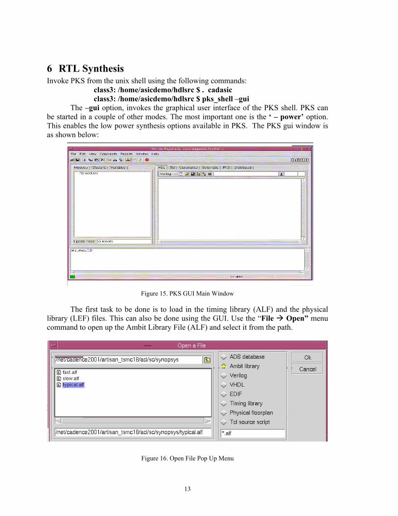
The –gui option, invokes the graphical user interface of the PKS shell. PKS can be started in a couple of other modes. The most important one is the ‘ – power’ option. This enables the low power synthesis options available in PKS. The PKS gui window is as shown below:
Figure 15. PKS GUI Main Window
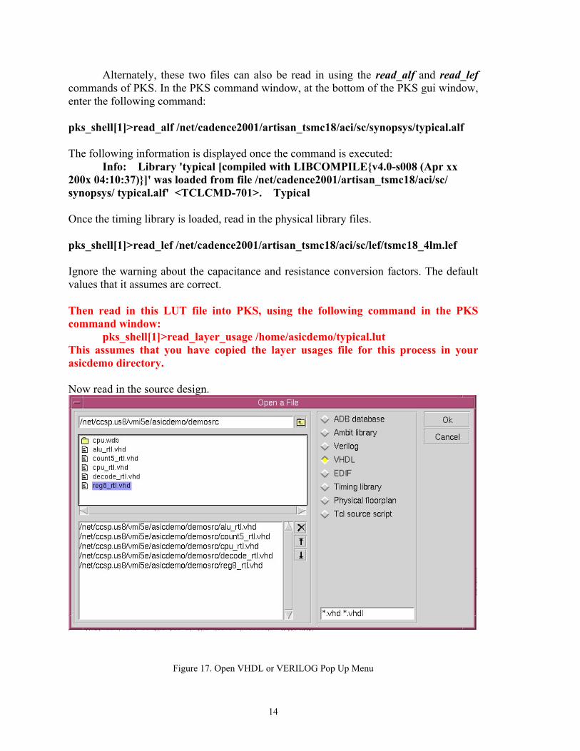
The first task to be done is to load in the timing library (ALF) and the physical library (LEF) files. This can also be done using the GUI. Use the “File Open” menu command to open up the Ambit Library File (ALF) and select it from the path.
Figure 16. Open File Pop Up Menu
13
Alternately, these two files can also be read in using the read_alf and read_lef commands of PKS. In the PKS command window, at the bottom of the PKS gui window, enter the following command: pks_shell[1]>read_alf /net/cadence2001/artisan_tsmc18/aci/sc/synopsys/typical.alf The following information is displayed once the command is executed:
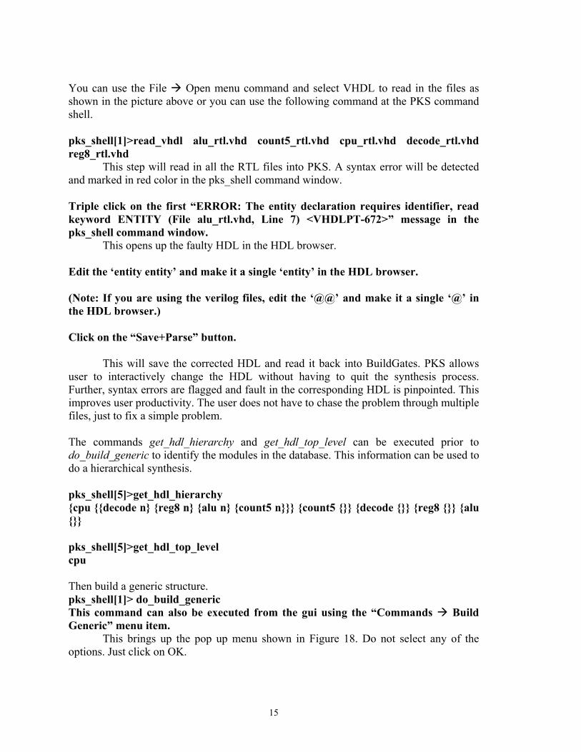
Info: Library 'typical [compiled with LIBCOMPILE{v4.0-s008 (Apr xx 200x 04:10:37)}]' was loaded from file /net/cadence2001/artisan_tsmc18/aci/sc/ synopsys/ typical.alf' <TCLCMD-701>. Typical Once the timing library is loaded, read in the physical library files. pks_shell[1]>read_lef /net/cadence2001/artisan_tsmc18/aci/sc/lef/tsmc18_4lm.lef Ignore the warning about the capacitance and resistance conversion factors. The default values that it assumes are correct. Then read in this LUT file into PKS, using the following command in the PKS command window: pks_shell[1]>read_layer_usage /home/asicdemo/typical.lut This assumes that you have copied the layer usages file for this process in your asicdemo directory. Now read in the source design.
Figure 17. Open VHDL or VERILOG Pop Up Menu
14
You can use the File Open menu command and select VHDL to read in the files as shown in the picture above or you can use the following command at the PKS command shell. pks_shell[1]>read_vhdl alu_rtl.vhd count5_rtl.vhd cpu_rtl.vhd decode_rtl.vhd reg8_rtl.vhd
This step will read in all the RTL files into PKS. A syntax error will be detected and marked in red color in the pks_shell command window.
Triple click on the first “ERROR: The entity declaration requires identifier, read keyword ENTITY (File alu_rtl.vhd, Line 7) <VHDLPT-672>” message in the pks_shell command window.
This opens up the faulty HDL in the HDL browser. Edit the ‘entity entity’ and make it a single ‘entity’ in the HDL browser. (Note: If you are using the verilog files, edit the ‘@@’ and make it a single ‘@’ in the HDL browser.) Click on the “Save+Parse” button.
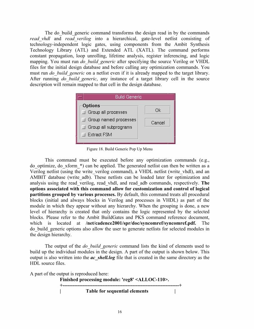
This will save the corrected HDL and read it back into BuildGates. PKS allows user to interactively change the HDL without having to quit the synthesis process. Further, syntax errors are flagged and fault in the corresponding HDL is pinpointed. This improves user productivity. The user does not have to chase the problem through multiple files, just to fix a simple problem. The commands get_hdl_hierarchy and get_hdl_top_level can be executed prior to do_build_generic to identify the modules in the database. This information can be used to do a hierarchical synthesis. pks_shell[5]>get_hdl_hierarchy {cpu {{decode n} {reg8 n} {alu n} {count5 n}}} {count5 {}} {decode {}} {reg8 {}} {alu {}} pks_shell[5]>get_hdl_top_level cpu Then build a generic structure. pks_shell[1]> do_build_generic This command can also be executed from the gui using the “Commands Build Generic” menu item. This brings up the pop up menu shown in Figure 18. Do not select any of the options. Just click on OK.
15
The do_build_generic command transforms the design read in by the commands read_vhdl and read_verilog into a hierarchical, gate-level netlist consisting of technology-independent logic gates, using components from the Ambit Synthesis Technology Library (ATL) and Extended ATL (XATL). The command performs constant propagation, loop unrolling, lifetime analysis, register inferencing, and logic mapping. You must run do_build_generic after specifying the source Verilog or VHDL files for the initial design database and before calling any optimization commands. You must run do_build_generic on a netlist even if it is already mapped to the target library. After running do_build_generic, any instance of a target library cell in the source description will remain mapped to that cell in the design database.
Figure 18. Build Generic Pop Up Menu
This command must be executed before any optimization commands (e.g.,
do_optimize, do_xform_*) can be applied. The generated netlist can then be written as a Verilog netlist (using the write_verilog command), a VHDL netlist (write_vhdl), and an AMBIT database (write_adb). These netlists can be loaded later for optimization and analysis using the read_verilog, read_vhdl, and read_adb commands, respectively. The options associated with this command allow for customization and control of logical partitions grouped by various processes. By default, this command treats all procedural blocks (initial and always blocks in Verilog and processes in VHDL) as part of the module in which they appear without any hierarchy. When the grouping is done, a new level of hierarchy is created that only contains the logic represented by the selected blocks. Please refer to the Ambit BuildGates and PKS command reference document, which is located at /net/cadence2001/spr/doc/syncomref/syncomref.pdf. The do_build_generic options also allow the user to generate netlists for selected modules in the design hierarchy.
The output of the do_build_generic command lists the kind of elements used to build up the individual modules in the design. A part of the output is shown below. This output is also written into the ac_shell.log file that is created in the same directory as the HDL source files. A part of the output is reproduced here:
Finished processing module: 'reg8' <ALLOC-110>. +----------------------------------------------------------------------+ | Table for sequential elements |
16
|----------------------------------------------------------------------| | File Name | Line | Register | Type | Width | AS | AR | SS | SR | | | | Name | | | | | | | |--------------+------+-------------+------+-------+----+----+----+----| | reg8_rtl.vhd | 19 | dataOut_reg | D_FF | 8 | N | Y | N | N | +----------------------------------------------------------------------+ Created 8-bit carry-lookahead arithmetic component <AWARE-004>. Finished processing module: 'alu' <ALLOC-110>. +--------------------------------------------------------------------+ | Table for sequential elements | |--------------------------------------------------------------------| | File Name | Line | Register | Type | Width | AS | AR | SS | SR | | | | Name | | | | | | | |-------------+------+------------+------+-------+----+----+----+----| | alu_rtl.vhd | 25 | zero_reg | D_FF | 1 | N | Y | N | N | |-------------+------+------------+------+-------+----+----+----+----| | alu_rtl.vhd | 25 | aluout_reg | D_FF | 8 | N | Y | N | N | +--------------------------------------------------------------------+ Finished processing module: 'decode' <ALLOC-110>. +----------------------------------------------------------------------+ | Table for sequential elements | |----------------------------------------------------------------------| | File Name | Line | Register | Type | Width | AS | AR | SS | SR | | | | Name | | | | | | | |----------------+------+-----------+------+-------+----+----+----+----| | decode_rtl.vhd | 30 | state_reg | D_FF | 3 | N | Y | N | N | +----------------------------------------------------------------------+ Created 5-bit carry-lookahead arithmetic component <AWARE-004>. Finished processing module: 'count5' <ALLOC-110>. +---------------------------------------------------------------------+ | Table for sequential elements | |---------------------------------------------------------------------| | File Name | Line | Register | Type | Width | AS | AR | SS | SR | | | | Name | | | | | | | |----------------+------+----------+------+-------+----+----+----+----| | count5_rtl.vhd | 24 | qout_reg | D_FF | 5 | N | Y | N | N | +---------------------------------------------------------------------+
The tables describe the registers used in building the design. • File : Name Description • Line : Line number in the source of register in the RTL description • Register Name : The name used for this register in the netlist. • Type : The generic cell chosen to implement this register. • Width : The width of the register. • AS : Specifies if this register has an Asynchronous Set control (Y or N). • AR : Specifies if this register has an Asynchronous Reset control (Y or N). • SS : Specifies if this register has an Asynchronous Set control (Y or N).
17

• SR : Specifies if this register has an Asynchronous Reset control (Y or N).
Go through the ac_shell.log file to get an idea about the kind of netlist that the do_build_generic command has generated for the design.
Also notice the module hierarchy displayed under the Modules tab window in the center left of the main window. The state of the module is displayed in parenthesis after the name of the module. The following are the definitions of the states displayed:
b: Black Box g: Contains Generic View m: Contains Mapped View o: Contains Optimized View x: Module is marked as “don’t modify”.
In case the VHDL code contains case statements, the log file will contain information about the case statement in the source code. It will describe the elements used to build the case statement.
Figure 19. Hierarchical Modules after Building a Generic Netlist.
Notice that at this stage, all the modules contain a generic view.
18
You can see the schematics for each of the modules. Select any of the modules and right click on them. Select the “Open Schematic Main Window” option and the schematic is displayed under the “Schematic” tab on the right side. This can also be done in the following method: Double-click on the “cpu” item at the root of the hierarchy tree.
This shows the schematic of the design in the schematic viewer. Drag the left mouse button (move cursor down/right) over the lower right quadrant of the schematic.
You’re now zoomed in on the ALU1 and PCOUNT1 modules. Right mouse clicking on the ALU1 module and select “Open HDL New Window”
The line in the RTL code that generated the MUX gate is highlighted. This way you can view the gates and associated HDL constructs. Click on the “Close” button in the HDL window that had popped up.
In this way, NaviGates, which is the name of the PKS main window browser, allows the user to trace the constructs in the generic netlist, back to RTL. The designer can now experiment new constructs in the HDL and easily correlate the effects in the netlist.
The schematic for the CPU module is shown below.
19
Figure 20. Schematic of the Generated Hierarchical Netlist TIP: Notice that there are 3 main windows within the PKS GUI. The window on the center left consists of the “Module”, “Clusters” and “Variables” tabs. The one on the center right consists of the “HDL”, “Tcl”, “constraints”, “Schematics”, “PKS”, and “Distributed” tabs. Finally, the one at the bottom is the pks command shell window. In order to expand the views of either of the windows, select the window by clicking in them and then do a “CTRL+m”. Use the same “CTRL+m” to reduce the size back to normal.
6.1 Creating a Flattened Netlist (Note: this section must be done in a a separate tutorial. You can skip this section without causing any problem to your current tutorial. )
A flattened netlist is one in which all of the modules are collapsed into the top level of the hierarchy. For example, if you flatten the CPU design, there is only one module (cpu), and all of the submodules are contained within it. Flattened netlists are often necessary at the physical design stage, because many layout and place-and-route tools cannot handle hierarchical netlists. Flattening a netlist places all of the modules within the top-level module. That is, it removes the hierarchy from the design. This is often necessary before using the netlist with back-end tools, such as a layout or place-and-route tool, because this type of tool cannot usually handle hierarchical netlists. However, you can flatten a design at any time during development, because flattening can let the synthesis tool perform additional optimizations. To flatten the netlist: In the Modules tab, select “cpu”, right click and choose “Set Current Module” from the pop-up menu. In the command area, enter the following command:
do_dissolve_hierarchy -hierarchical The GUI displays the flattened netlist, as shown below. Compare this with the hierarchical modules shown in Figure [* *]. Also, compare the schematics and placements of the hierarchical and flattened netlists.
20
7 FloorPlanning Once the generic netlist is generated for the design, we can proceed to the
floorplanning stage. Please note that PKS does not allow you to define the floorplan before you execute the do_build_generic command. The floorplanning parameters can be set using the GUI or by entering the commands individually at the pks command shell.
Click on the PKS tab in the center right side of the screen. Then do a right click and select the “Define Floorplan..” option. This brings up the floorplan pop up menu shown below.
Figure 21. Default Floorplan Options
For this particular example, do not change any of the parameters. For any of your future designs, experiment with these various floorplanning parameters.
You can set the same floorplanning parameters using the set_floorplan_parameters command. Refer to the command reference manual for details of all the parameters that you can set using this command.
21
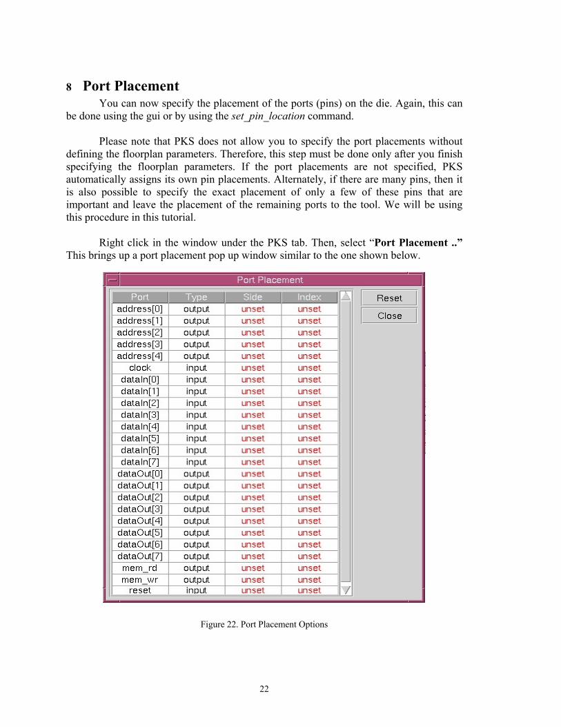
8 Port Placement You can now specify the placement of the ports (pins) on the die. Again, this can
be done using the gui or by using the set_pin_location command. Please note that PKS does not allow you to specify the port placements without
defining the floorplan parameters. Therefore, this step must be done only after you finish specifying the floorplan parameters. If the port placements are not specified, PKS automatically assigns its own pin placements. Alternately, if there are many pins, then it is also possible to specify the exact placement of only a few of these pins that are important and leave the placement of the remaining ports to the tool. We will be using this procedure in this tutorial.
Right click in the window under the PKS tab. Then, select “Port Placement ..” This brings up a port placement pop up window similar to the one shown below.
Figure 22. Port Placement Options
22
“For this particular example, do not set any ports. Just click on the “Close” button. For your future designs, you can set the “Side” to be either ‘top’, ‘bottom’, ‘left’ or ‘right’ for each port. The “Index” refers to the position number of the pin. The pins are numbered left to right, starting from 1, for the top and bottom pins. The numbering goes from bottom to top, starting from 1, for the left and right side pins.”
9 Constraints Once the floorplanning specifications and port placements are set, the timing
constraints must be specified before performing the optimizations. Click on the “Constraints” tab on the center right window.
This displays the properties related to the clock and timing constraints. The top
portion of this tab contains two tables—one that defines the ideal clock, and one that binds the clock ports of module instances to the ideal clock. If only the ideal clock table appears, use the split-pane slider to make both tables appear.
For all sequential logic, you specify timing constraints with respect to an ideal
clock. An ideal clock lets the logic synthesis process determine the intended relationship between various clocks and clock ports. You define the period and cycle duty for an ideal clock, using the “set_clock” command. For example, the command: set_clock clk1 -period 4 -waveform “0 2” ; the set_clock command defines an ideal clock named clk1. This ideal clock has a period of 4ns, a rising edge of 0ns, and a falling edge of 2ns. This can be done using the GUI as well.
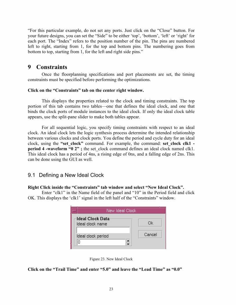
9.1 Defining a New Ideal Clock Right Click inside the “Constraints” tab window and select “New Ideal Clock”.
Enter “clk1” in the Name field of the panel and “10” in the Period field and click OK. This displays the ‘clk1’ signal in the left half of the “Constraints” window.
Figure 23. New Ideal Clock Click on the “Trail Time” and enter “5.0” and leave the “Lead Time” as “0.0”
23
You have now created an ideal clock of period 10 ns with leading edge at 0 ns and trailing edge at 5ns. All the data arrival and required times will be constrained using this ideal clock.
9.2 Binding a Port to a Clock
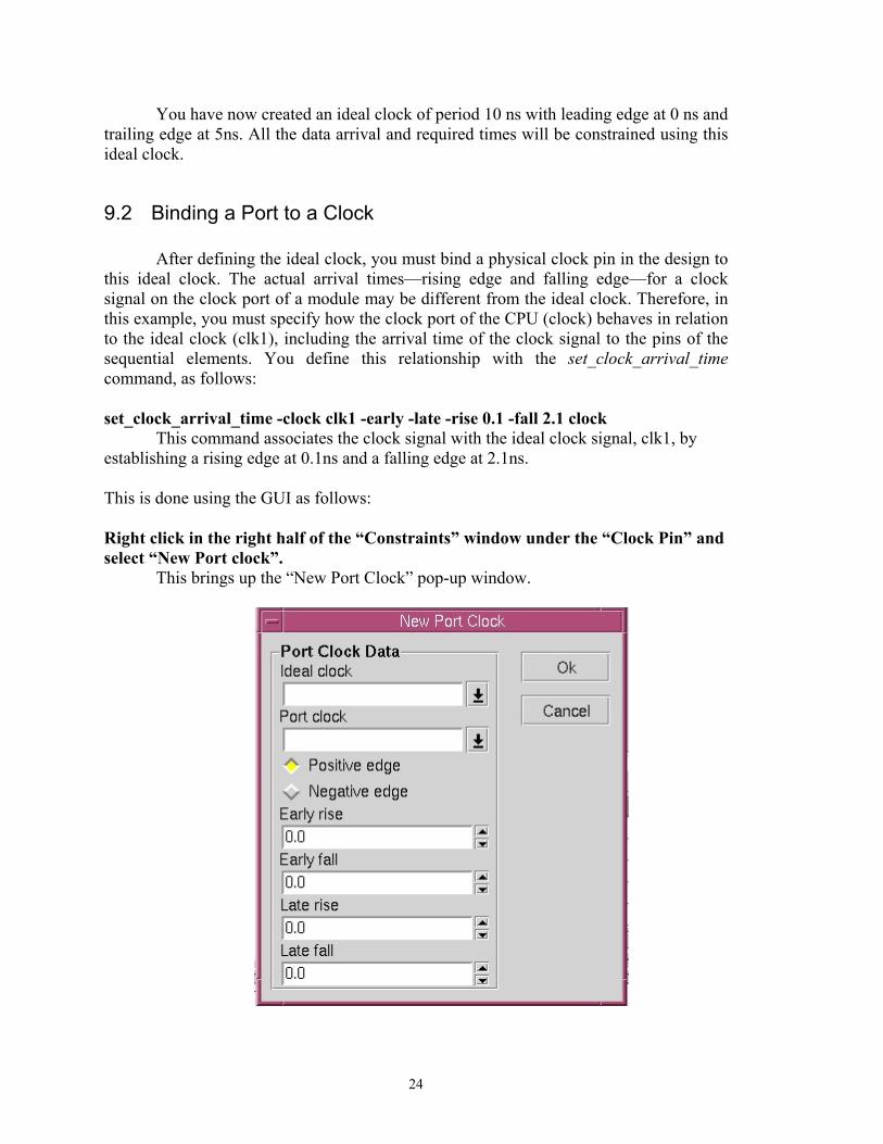
After defining the ideal clock, you must bind a physical clock pin in the design to this ideal clock. The actual arrival times—rising edge and falling edge—for a clock signal on the clock port of a module may be different from the ideal clock. Therefore, in this example, you must specify how the clock port of the CPU (clock) behaves in relation to the ideal clock (clk1), including the arrival time of the clock signal to the pins of the sequential elements. You define this relationship with the set_clock_arrival_time command, as follows: set_clock_arrival_time -clock clk1 -early -late -rise 0.1 -fall 2.1 clock
This command associates the clock signal with the ideal clock signal, clk1, by establishing a rising edge at 0.1ns and a falling edge at 2.1ns. This is done using the GUI as follows: Right click in the right half of the “Constraints” window under the “Clock Pin” and select “New Port clock”.
This brings up the “New Port Clock” pop-up window.
24
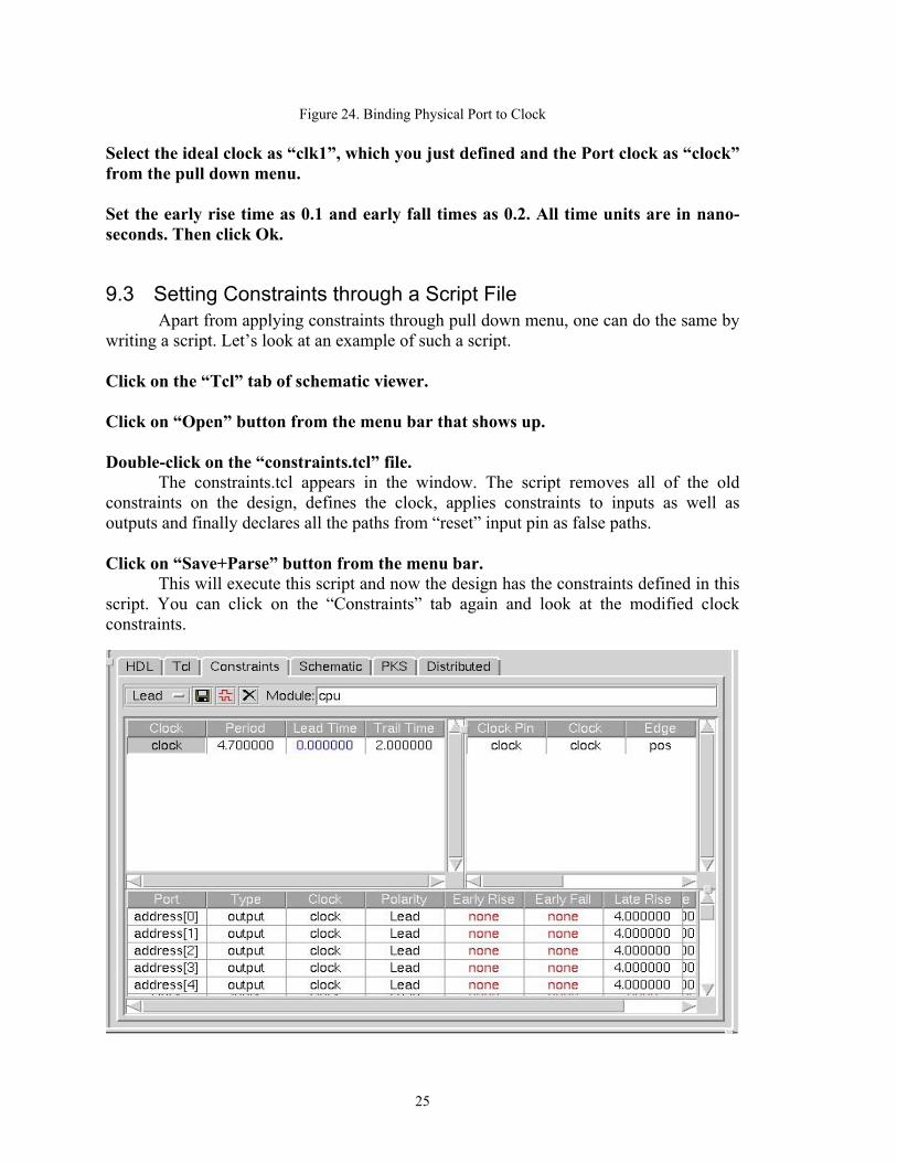
Figure 24. Binding Physical Port to Clock
Select the ideal clock as “clk1”, which you just defined and the Port clock as “clock” from the pull down menu. Set the early rise time as 0.1 and early fall times as 0.2. All time units are in nano-seconds. Then click Ok.
9.3 Setting Constraints through a Script File Apart from applying constraints through pull down menu, one can do the same by
writing a script. Let’s look at an example of such a script. Click on the “Tcl” tab of schematic viewer.
Click on “Open” button from the menu bar that shows up.
Double-click on the “constraints.tcl” file.
The constraints.tcl appears in the window. The script removes all of the old constraints on the design, defines the clock, applies constraints to inputs as well as outputs and finally declares all the paths from “reset” input pin as false paths. Click on “Save+Parse” button from the menu bar.
This will execute this script and now the design has the constraints defined in this script. You can click on the “Constraints” tab again and look at the modified clock constraints.
25

Figure 25. Constraints Tab The constraints that have been set can be viewed in the schematic of the design. Click on the “Schematic” tab of schematic viewer.
Click on the port named “mem_rd”
Then right-click the mouse button for pop-up menu.
Select “Show Constraints” in the popup menu.
A window showing all the constraints on the port pops up. This is an easy-to-us interactive way of looking at constraints on ports of the design.
26
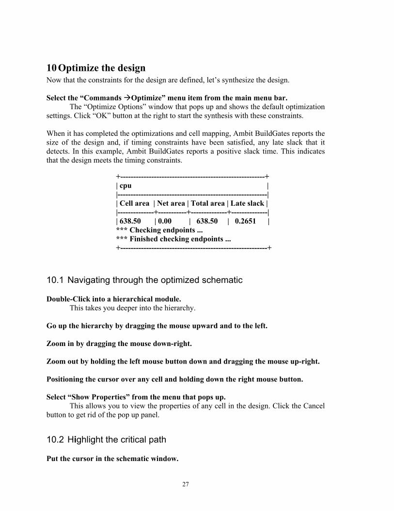
10 Optimize the design Now that the constraints for the design are defined, let’s synthesize the design. Select the “Commands Optimize” menu item from the main menu bar.
The “Optimize Options” window that pops up and shows the default optimization settings. Click “OK” button at the right to start the synthesis with these constraints. When it has completed the optimizations and cell mapping, Ambit BuildGates reports the size of the design and, if timing constraints have been satisfied, any late slack that it detects. In this example, Ambit BuildGates reports a positive slack time. This indicates that the design meets the timing constraints.
+--------------------------------------------------------+ | cpu | |----------------------------------------------------------| | Cell area | Net area | Total area | Late slack | |--------------+-----------+--------------+--------------| | 638.50 | 0.00 | 638.50 | 0.2651 | *** Checking endpoints ... *** Finished checking endpoints ... +---------------------------------------------------------+
10.1 Navigating through the optimized schematic Double-Click into a hierarchical module.
This takes you deeper into the hierarchy. Go up the hierarchy by dragging the mouse upward and to the left.
Zoom in by dragging the mouse down-right. Zoom out by holding the left mouse button down and dragging the mouse up-right. Positioning the cursor over any cell and holding down the right mouse button. Select “Show Properties” from the menu that pops up.
This allows you to view the properties of any cell in the design. Click the Cancel button to get rid of the pop up panel.
10.2 Highlight the critical path Put the cursor in the schematic window.
27
Use the right mouse button to bring up the menu. Select “Worst Path”.
The worst slack path in the design will be highlighted. Double-click on one of the hierarchical instances in the worst path. Zoom in on the highlighted gates.
You see the arrival times on the pins of the instances. With the timing numbers on the path itself, it is very easy to understand the cause of delays and fix any issues. (This may not work in PKS. If you run BuildGates individually, it may work.)
Use the right mouse button to bring up the menu. Select “Worst Endpoint / 5”.
This will highlight the worst five endpoints in the current design with the corresponding timing numbers. Select “Clear” from menus at the top of schematic window to clear the highlighting. Click on one of the gates; use the right mouse button to bring up the menu. Select “Fan-in cone”.
This will highlight the fan-in cone to that particular pin.
Zoom in on the highlighted gates in the cone. You can see the arrival times from various paths. NaviGates allows user to easily
track worst paths, worst endpoints in the design. You can also trace fan-in and fanout cones of logic. The timing numbers for all the arrivals are right there on the instances making it easier to locate problem spots in the design. At this point, you must save some of the results generated so far. You must save the timing report, vhdl netlist file, the ambit database file and the DEF file containing the physical design data.
10.3 Generating Reports To Generate the Timing Report: Right-click on the “cpu” in module hierarchy and right click on it. Select “Set Current Module” and “Set Top Timing Module”
This will make “cpu” the current module.
Select the “Reports Report Timing..” menu from the main menu. Click “Generate Report” button at the top right hand side of the Report window.
28
Now the generation of timing report is initiated. The timing report describes in detail the worst path in the design. It identifies the begin-and-endpoint, instance-by-instance delays, logic arcs and the cumulative delays.
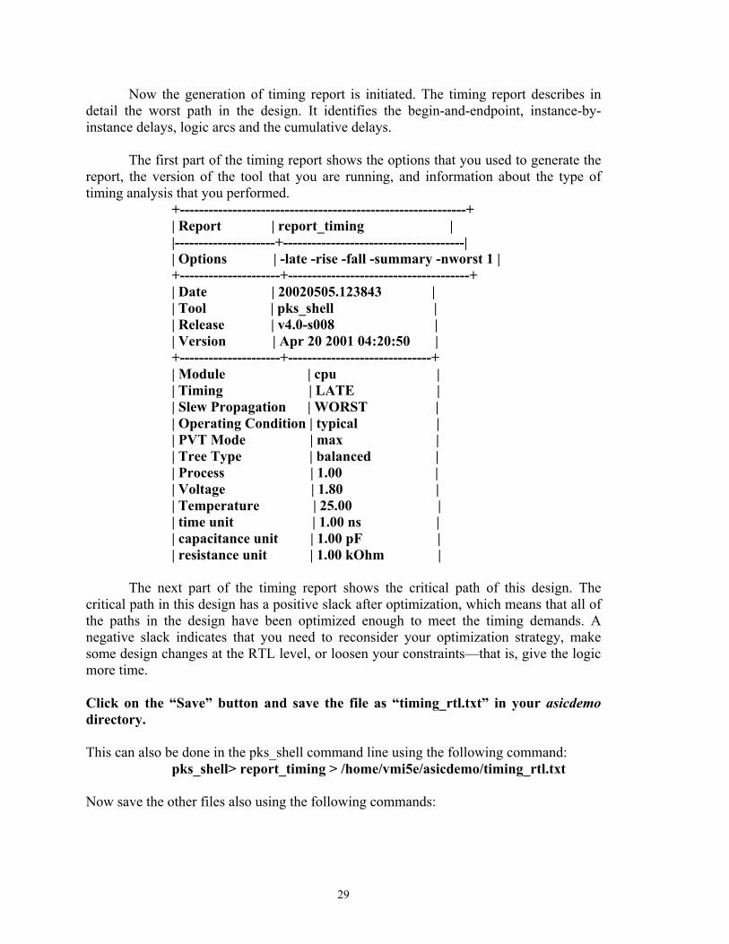
The first part of the timing report shows the options that you used to generate the report, the version of the tool that you are running, and information about the type of timing analysis that you performed.
+------------------------------------------------------------+ | Report | report_timing | |---------------------+--------------------------------------| | Options | -late -rise -fall -summary -nworst 1 | +---------------------+--------------------------------------+ | Date | 20020505.123843 | | Tool | pks_shell | | Release | v4.0-s008 | | Version | Apr 20 2001 04:20:50 | +---------------------+------------------------------+ | Module | cpu | | Timing | LATE | | Slew Propagation | WORST | | Operating Condition | typical | | PVT Mode | max | | Tree Type | balanced | | Process | 1.00 | | Voltage | 1.80 | | Temperature | 25.00 | | time unit | 1.00 ns | | capacitance unit | 1.00 pF | | resistance unit | 1.00 kOhm |
The next part of the timing report shows the critical path of this design. The critical path in this design has a positive slack after optimization, which means that all of the paths in the design have been optimized enough to meet the timing demands. A negative slack indicates that you need to reconsider your optimization strategy, make some design changes at the RTL level, or loosen your constraints—that is, give the logic more time. Click on the “Save” button and save the file as “timing_rtl.txt” in your asicdemo directory. This can also be done in the pks_shell command line using the following command:
pks_shell> report_timing > /home/vmi5e/asicdemo/timing_rtl.txt Now save the other files also using the following commands:
29

pks_shell[5]> write_adb /home/vmi5e/asicdemo/demo_rtl.adb pks_shell[5]>write_verilog -hier /home/vmi5e/asicdemo/demo_rtl.v pks_shell[5]>write_def /home/vmi5e/asicdemo/demo_rtl.def
The Ambit database file contains design, floorplan and constraint information.
The DEF file contains the flat physical data containing initial floorplanning and power design information
Using the “Reports Area..” menu from the main menu, you can generate and save the area reports also. Also look out for the “Reports DRC..” menu from the main menu for the DRC rules violations report.
At this point, you have saved all your design in the database file (.adb) and the DEF file. You can exit out of PKS, come back later, and re-load the saved design.
When you come back, restart PKS and first read in the ALF and LEF files. After that click on the File Open menu and open the demo_rtl.adb file that you had saved. This should bring you back to where you were in the last session.
30
11 Clock Tree Generation (CTPKS) Before beginning with the Clock Tree Generation, the optimized and mapped netlist must be fully placed. The timing library files (TLF, ALF), a physical library file (LEF), and a layer utilization table (LUT) must be loaded. 1.Specify default new clock components and net names as: set_global instance_generator "ctpks_CLK_%d" set_global net_generator "ctpks_net_CLK_%d" 2.Generate default clock tree constraints with specified clock roots.
set_clock_tree_constraints -pin [find –port CLK] -min_delay 2.0 -max_delay 2.5 –max_skew 0.3 -max_leaf_transition 1.0
These are default numbers and can be modified based on the characteristics of the particular clock in the design. A message is seen in the console window indicating the setting up of the clock with these parameters. 3. Define the clock tree boundary. The design is now made unique by running the command do_uniquely_instantiate. It will then traverse through the netlist and find the boundary of a clock tree with the clock root specified by the user. do_uniquely_instantiate Make sure the dont_modify property has not been set on any cell in the clock networks and clock roots. 4. Set clock root and build clock tree. The root is set to the pin that serves as clock root.
set_clock_root -clock clk1 clock do_build_clock_tree -noplace -pin [find -port clock]
A message similar to the one shown below will be displayed in the console window if the command is successful. Note that the number of violations is reported as well. In this example, there are no violations. In typical cases, there will be timing violations that will require to be fixed.
31
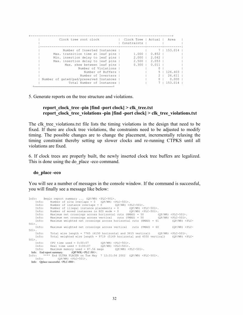
+--------------------------------------------------------------------------+ | Clock tree root clock | Clock Tree | Actual | Area | | | Constraints | | | |-----------------------------------------+-------------+--------+---------| | Number of Inserted Instances | | 7 | 153.014 | | Max. transition time at leaf pins | 1.000 | 0.852 | | | Min. insertion delay to leaf pins | 2.000 | 2.042 | | | Max. insertion delay to leaf pins | 2.500 | 2.053 | | | Max. skew between leaf pins | 0.300 | 0.011 | | | Number of Violations | | 0 | | | Number of Buffers | | 5 | 126.403 | | Number of Inverters | | 2 | 26.611 | | Number of gated/pad/preserved Instances | | 0 | 0.000 | | Total Number of Instances | | 7 | 153.014 | +--------------------------------------------------------------------------+ 5. Generate reports on the tree structure and violations.
report_clock_tree -pin [find -port clock] > clk_tree.txt report_clock_tree_violations -pin [find -port clock] > clk_tree_violations.txt
The clk_tree_violations.txt file lists the timing violations in the design that need to be fixed. If there are clock tree violations, the constraints need to be adjusted to modify timing. The possible changes are to change the placement, incrementally relaxing the timing constraint thereby setting up slower clocks and re-running CTPKS until all violations are fixed. 6. If clock trees are properly built, the newly inserted clock tree buffers are legalized. This is done using the do_place -eco command. do_place -eco You will see a number of messages in the console window. If the command is successful, you will finally see a message like below: Info: Begin report summary ... (QP/WR) <PLC-501>. Info: Number of site overlaps = 0 (QP/WR) <PLC-501>. Info: Number of instance overlaps = 0 (QP/WR) <PLC-501>. Info: Number of illegal instance placements = 0 (QP/WR) <PLC-501>. Info: Number of moved instances in ECO mode = 0 (QP/WR) <PLC-501>. Info: Maximum net crossings across horizontal cuts (HMAX) = 50 (QP/WR) <PLC-501>. Info: Maximum net crossings across vertical cuts (VMAX) = 50 (QP/WR) <PLC-501>. Info: Maximum weighted net crossings across horizontal cuts (HMAX) = 61 (QP/WR) <PLC-501>. Info: Maximum weighted net crossings across vertical cuts (VMAX) = 60 (QP/WR) <PLC-501>. Info: Total wire length = 7765 (4150 horizontal and 3615 vertical) (QP/WR) <PLC-501>. Info: Total weighted wire length = 9719 (5169 horizontal and 4550 vertical) (QP/WR) <PLC-501>. Info: CPU time used = 0:00:07 (QP/WR) <PLC-501>. Info: Real time used = 0:00:07 (QP/WR) <PLC-501>. Info: Maximum memory used = 87.56 megs (QP/WR) <PLC-501>. Info: End report summary. (QP/WR) <PLC-501>. Info: **** End ULTRA PLACER on Tue May 7 12:31:56 2002 (QP/WR) <PLC-501>. Info: (QP/WR) <PLC-501>. Info: Qplace successful. <PLC-888>.
32
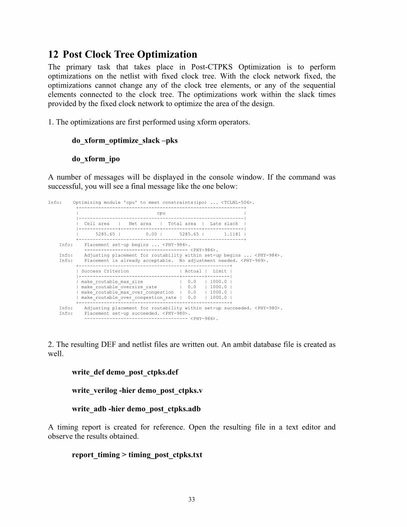
12 Post Clock Tree Optimization The primary task that takes place in Post-CTPKS Optimization is to perform optimizations on the netlist with fixed clock tree. With the clock network fixed, the optimizations cannot change any of the clock tree elements, or any of the sequential elements connected to the clock tree. The optimizations work within the slack times provided by the fixed clock network to optimize the area of the design. 1. The optimizations are first performed using xform operators. do_xform_optimize_slack –pks do_xform_ipo A number of messages will be displayed in the console window. If the command was successful, you will see a final message like the one below: Info: Optimizing module 'cpu' to meet constraints(ipo) ... <TCLNL-506>. +-----------------------------------------------------------+ | cpu | |-----------------------------------------------------------| | Cell area | Net area | Total area | Late slack | |--------------+--------------+--------------+--------------| | 5285.65 | 0.00 | 5285.65 | 1.1181 | +-----------------------------------------------------------+ Info: Placement set-up begins ... <PHY-984>. ------------------------------------- <PHY-986>. Info: Adjusting placement for routability within set-up begins ... <PHY-984>. Info: Placement is already acceptable. No adjustment needed. <PHY-969>. +------------------------------------------------------+ | Success Criterion | Actual | Limit | |------------------------------------+--------+--------| | make_routable_max_size | 0.0 | 1000.0 | | make_routable_oversize_rate | 0.0 | 1000.0 | | make_routable_max_over_congestion | 0.0 | 1000.0 | | make_routable_over_congestion_rate | 0.0 | 1000.0 | +------------------------------------------------------+ Info: Adjusting placement for routability within set-up succeeded. <PHY-980>. Info: Placement set-up succeeded. <PHY-980>. ------------------------------------- <PHY-986>.
2. The resulting DEF and netlist files are written out. An ambit database file is created as well. write_def demo_post_ctpks.def write_verilog -hier demo_post_ctpks.v write_adb -hier demo_post_ctpks.adb A timing report is created for reference. Open the resulting file in a text editor and observe the results obtained.
report_timing > timing_post_ctpks.txt
33
13 Global Routing and Post-Global route Optimizations This step involves running the global route portion of Wroute inside the Cadence physically knowledgeable synthesis (PKS) timing environment. The initial timing for global route optimization is based on the fast route estimate done inside the PKS tool. For subsequent optimization passes of the global route, the timing is based on RC information derived from the actual routes.
During global routing, the router interconnects the regular (signal) nets for the design, based on the supply and demand of routing tracks. It finds generalized pathways, without laying down actual wires, and makes iterative passes to optimize the global routing, shorten wire length, and minimize the use of vias. During global routing, the router also updates the congestion map.
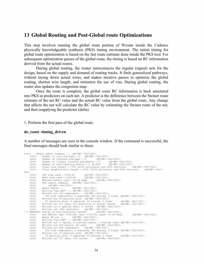
Once the route is complete, the global route RC information is back annotated into PKS as predictors on each net. A predictor is the difference between the Steiner route estimate of the net RC value and the actual RC value from the global route. Any change that affects the net will calculate the RC value by estimating the Steiner route of the net, and then reapplying the predictor (delta). 1. Perform the first pass of the global route. do_route -timing_driven A number of messages are seen in the console window. If the command is successful, the final messages should look similar to these: Info: Begin report summary ... (QP/WR) <PLC-501>. Info: Number of site overlaps = 0 (QP/WR) <PLC-501>. Info: Number of instance overlaps = 0 (QP/WR) <PLC-501>. Info: Number of illegal instance placements = 0 (QP/WR) <PLC-501>. Info: Number of over-capacity gCells = 0 (0.00%) (QP/WR) <PLC-501>. Info: Total wire length = 7765 (4150 horizontal and 3615 vertical) (QP/WR) <PLC-501>. Info: Total weighted wire length = 9719 (5169 horizontal and 4550 vertical) (QP/WR) <PLC-501>. Info: CPU time used = 0:00:08 (QP/WR) <PLC-501>. Info: Real time used = 0:00:09 (QP/WR) <PLC-501>. Info: Maximum memory used = 87.56 megs (QP/WR) <PLC-501>. Info: End report summary. (QP/WR) <PLC-501>. Info: (QP/WR) <PLC-501>. Info: Begin DEFout ... (QP/WR) <PLC-501>. Info: Writing "cpu.def" ... (QP/WR) <PLC-501>. Info: Written out 205 components (QP/WR) <PLC-501>. Info: 205 core components: 0 unplaced, 205 placed, 0 fixed (QP/WR) <PLC-501>. Info: Written out 25 physical pins (QP/WR) <PLC-501>. Info: 25 physical pins: 0 unplaced, 25 placed, 0 fixed (QP/WR) <PLC-501>. Info: Written out 217 nets, 215 partially or global routed (QP/WR) <PLC-501>. Info: Written out 2 special nets, 2 routed (QP/WR) <PLC-501>. Info: Written out 1240 terminals (QP/WR) <PLC-501>. --> WARNING: Design is only partially routed! (QP/WR) <PLC-502>. Info: End DEFout: cpu: 0:00:00, real: 0:00:00, peak: 87.56 megs. (QP/WR) <PLC-501>. Info: Begin DB out ... (QP/WR) <PLC-501>. Info: Writing "cpu.wdb" ... (QP/WR) <PLC-501>. Info: Written out 9 layers, 4 routing layers, 1 overlap layer (QP/WR) <PLC-501>. Info: Written out 478 macros, 28 used (QP/WR) <PLC-501>. Info: Written out 205 components (QP/WR) <PLC-501>. Info: 205 core components: 0 unplaced, 205 placed, 0 fixed (QP/WR) <PLC-501>. Info: Written out 25 physical pins (QP/WR) <PLC-501>. Info: 25 physical pins: 0 unplaced, 25 placed, 0 fixed (QP/WR) <PLC-501>. Info: Written out 217 nets, 215 routed (QP/WR) <PLC-501>.
34
Info: Written out 2 special nets, 2 routed (QP/WR) <PLC-501>. Info: Written out 1240 terminals (QP/WR) <PLC-501>. Info: Written out 6708 gcells for 4 layers (QP/WR) <PLC-501>. Info: Written out 1200 real and virtual terminals (QP/WR) <PLC-501>. Info: Layer METAL1: Res = 4.39e-01 ohm/um, Cap = 2.06e-04 pF/um (PP model)(QP/WR) <PLC-501>.
Info: End DB out: cpu: 0:00:00, real: 0:00:02, peak: 87.56 megs. (QP/WR) <PLC-501>.
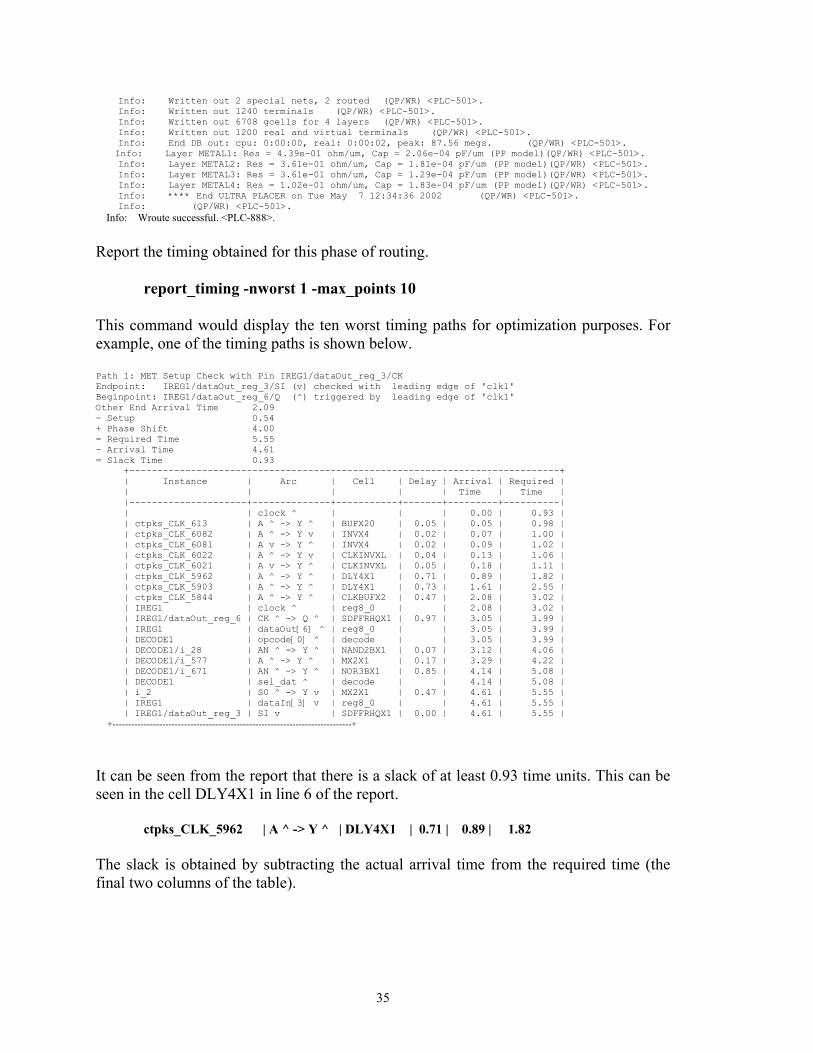
Info: Layer METAL2: Res = 3.61e-01 ohm/um, Cap = 1.81e-04 pF/um (PP model)(QP/WR) <PLC-501>. Info: Layer METAL3: Res = 3.61e-01 ohm/um, Cap = 1.29e-04 pF/um (PP model)(QP/WR) <PLC-501>. Info: Layer METAL4: Res = 1.02e-01 ohm/um, Cap = 1.83e-04 pF/um (PP model)(QP/WR) <PLC-501>. Info: **** End ULTRA PLACER on Tue May 7 12:34:36 2002 (QP/WR) <PLC-501>. Info: (QP/WR) <PLC-501>. Info: Wroute successful. <PLC-888>. Report the timing obtained for this phase of routing. report_timing -nworst 1 -max_points 10 This command would display the ten worst timing paths for optimization purposes. For example, one of the timing paths is shown below. Path 1: MET Setup Check with Pin IREG1/dataOut_reg_3/CK Endpoint: IREG1/dataOut_reg_3/SI (v) checked with leading edge of 'clk1' Beginpoint: IREG1/dataOut_reg_6/Q (^) triggered by leading edge of 'clk1' Other End Arrival Time 2.09 - Setup 0.54 + Phase Shift 4.00 = Required Time 5.55 - Arrival Time 4.61 = Slack Time 0.93 +-----------------------------------------------------------------------------+ | Instance | Arc | Cell | Delay | Arrival | Required | | | | | | Time | Time | |---------------------+--------------+-----------+-------+---------+----------| | | clock ^ | | | 0.00 | 0.93 | | ctpks_CLK_613 | A ^ -> Y ^ | BUFX20 | 0.05 | 0.05 | 0.98 | | ctpks_CLK_6082 | A ^ -> Y v | INVX4 | 0.02 | 0.07 | 1.00 | | ctpks_CLK_6081 | A v -> Y ^ | INVX4 | 0.02 | 0.09 | 1.02 | | ctpks_CLK_6022 | A ^ -> Y v | CLKINVXL | 0.04 | 0.13 | 1.06 | | ctpks_CLK_6021 | A v -> Y ^ | CLKINVXL | 0.05 | 0.18 | 1.11 | | ctpks_CLK_5962 | A ^ -> Y ^ | DLY4X1 | 0.71 | 0.89 | 1.82 | | ctpks_CLK_5903 | A ^ -> Y ^ | DLY4X1 | 0.73 | 1.61 | 2.55 | | ctpks_CLK_5844 | A ^ -> Y ^ | CLKBUFX2 | 0.47 | 2.08 | 3.02 | | IREG1 | clock ^ | reg8_0 | | 2.08 | 3.02 | | IREG1/dataOut_reg_6 | CK ^ -> Q ^ | SDFFRHQX1 | 0.97 | 3.05 | 3.99 | | IREG1 | dataOut[6] ^ | reg8_0 | | 3.05 | 3.99 | | DECODE1 | opcode[0] ^ | decode | | 3.05 | 3.99 | | DECODE1/i_28 | AN ^ -> Y ^ | NAND2BX1 | 0.07 | 3.12 | 4.06 | | DECODE1/i_577 | A ^ -> Y ^ | MX2X1 | 0.17 | 3.29 | 4.22 | | DECODE1/i_671 | AN ^ -> Y ^ | NOR3BX1 | 0.85 | 4.14 | 5.08 | | DECODE1 | sel_dat ^ | decode | | 4.14 | 5.08 | | i_2 | S0 ^ -> Y v | MX2X1 | 0.47 | 4.61 | 5.55 | | IREG1 | dataIn[3] v | reg8_0 | | 4.61 | 5.55 | | IREG1/dataOut_reg_3 | SI v | SDFFRHQX1 | 0.00 | 4.61 | 5.55 | +-----------------------------------------------------------------------------+ It can be seen from the report that there is a slack of at least 0.93 time units. This can be seen in the cell DLY4X1 in line 6 of the report.
ctpks_CLK_5962 | A ^ -> Y ^ | DLY4X1 | 0.71 | 0.89 | 1.82 The slack is obtained by subtracting the actual arrival time from the required time (the final two columns of the table).
35
2. Now an incremental optimization based on the parasitics obtained from the first global route step. These values are automatically passed to PKS after the first step and so a simple xform optimization is enough to use these back-annotated values.
do_xform_ipo Now another global route is performed based on the optimized results, and the results written to a wroute database.
do_route -timing_driven true -output_db_name demo_groute.wdb If the command is successful, a message is seen in the console window showing that the wroute was successful. Info: **** End ULTRA PLACER on Tue May 7 12:36:57 2002 (QP/WR) <PLC-501>. Info: (QP/WR) <PLC-501>. Info: Wroute successful. <PLC-888>. 3. The DEF, verilog netlist and ambit database files are written out for passing information to silicon Ensemble for detailed routing. write_def demo_groute.def write_verilog -hier demo_groute.v write_adb -hier demo_groute.adb 4. Exit PKS using the command quit. We will carry out the final routing using Silicon Ensemble.
36
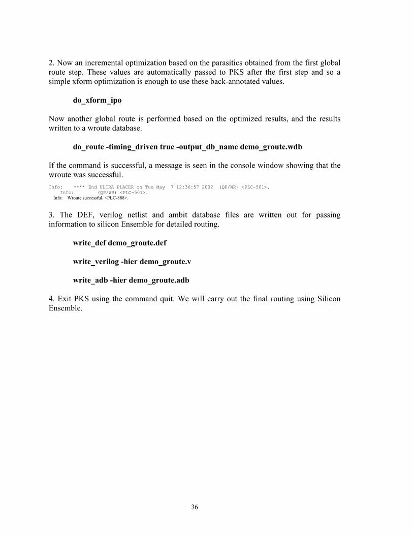
14 Detailed Routing
Start Silicon Ensemble by typing seultra at the unix shell command prompt. This will open up the silicon ensemble GUI. Spend some time familiarizing yourself with the GUI. You can perform floorplanning, placement and routing as well as verification using SE. The floorplanning and placement feature of SE is used in our flow, only in case there is a need for visually dragging and placing blocks in the die. We will perform only detailed routing using SE.
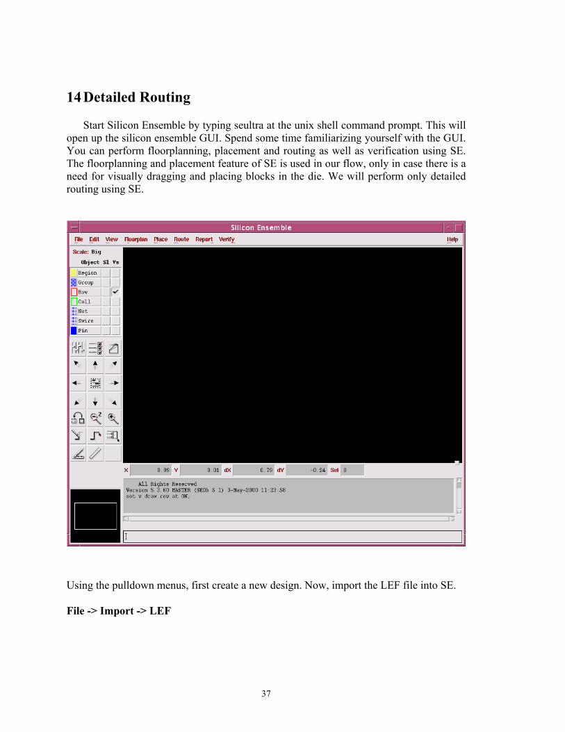
Using the pulldown menus, first create a new design. Now, import the LEF file into SE. File -> Import -> LEF
37
Now browse to the Artisan library folder containing the LEF files. /net/cadence2001/artisan_tsmc18/aci/sc/lef/tsmc18_41m.lef Now again use the IMPORT pull down menu to import your DEF file. File -> Import -> DEF The DEF file that must be imported is the demo_groute.def file that you created after global routing in PKS. Next, import the verilog netlist for you design. File -> Import -> Verilog The verilog file to be imported is the demo_groute.v file that you created after global routing in PKS. Now you are ready to carry out final routing. The first step is to carry out Power routing. Use the pull down menu under ROUTE. We will be using power rings for our routing as opposed to stripes. Route -> Plan Power -> Add rings
38
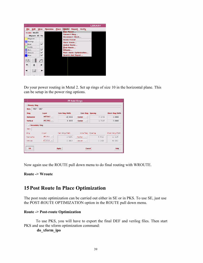
Do your power routing in Metal 2. Set up rings of size 10 in the horizontal plane. This can be setup in the power ring options.
Now again use the ROUTE pull down menu to do final routing with WROUTE. Route -> Wroute
15 Post Route In Place Optimization The post route optimization can be carried out either in SE or in PKS. To use SE, just use the POST-ROUTE OPTIMIZATION option in the ROUTE pull down menu. Route -> Post-route Optimization
To use PKS, you will have to export the final DEF and verilog files. Then start PKS and use the xform optimization command:
do_xform_ipo
39

References
1. Synthesis Place and Route Flow Guide located at /net/cadence2001/SPR40/ doc/sprflow/sprflow.pdf.
2. Ambit and Envisia Tutorial located at /net/cadence2001/LDV31/doc/ambittut orial/ambittutorial.pdf.
3. Ambit BuildGates Synthesis User Guide located at /net/cadence2001/ SPR40/doc/esug/esug.pdf.
4. PKS USER Guide located at /net/cadence2001/SPR40/doc/espks/espks.pdf. 5. Command Reference for Ambit BuildGates Synthesis and Cadence PKS
located at /net/cadence2001/SPR40/doc/syncomref/syncomref.pdf. 6. Low Power Option of Ambit BuildGates Synthesis and Cadence PKS located
at /net/cadence2001/SPR40/doc/synpwruser/synpwruser.pdf. 7. Timing Analysis for Ambit BuildGates Synthesis and Cadence PKS located at
/ net/cadence2001/SPR40/doc/synta/syntax.pdf. 8. Ambit BuildGates Synthesis Product Notes located at
/net/cadence2001/SPR40 /doc/esugpn/esugpn.pdf 9. Envisia Physically Knowledgeable Synthesis Product Notes located at
/net/cadence2001/SPR40/doc/espkspn/espkspn.pdf.
40