Embed Size (px)
Citation preview
THE DEVELOPMENT OF A TRANSIT RADIO TELESCOPE AT
THE HYDROGEN LINE FREQUENCY
Submitted in fulfillment of the academic requirements for the Master’s Degree of Technology: Electrical
Engineering – Light Current - Department of Electronic Engineering in the Faculty of Engineering and The
Built Environment at the Durban University of Technology
Aritha Pillay
JUNE 2012
____________________ ______________
Supervisor Date

ii
DECLARATION
I hereby declare that the contents of this thesis, entitled THE DEVELOPMENT OF A TRANSIT
RADIO TELESCOPE AT THE HYDROGEN LINE FREQUENCY, is a true reflection of my own work,
and that this thesis has not been submitted, in whole or part, for a degree to any other
University or Institution.
__________________ _____________
A Pillay Date
Student Number: 19301323
iii
ACKNOWLEDGEMENTS
I would like to acknowledge my supervisor and mentor Mr SD MacPherson for his words of
encouragement, constant motivation and support that he has given me. You are an inspiration and
without your constant guidance and expertise, what seemed like an enormous almost impossible task of
developing the radio telescope, would not have been successfully completed.
I would also like to acknowledge the staff at the Technology Station Design Unit at the Durban University
of Technology for their assistance in the manufacture of the parabolic reflector and feed horn. Your
attention to detail and accuracy has ensured that the manufacture and alignment of the parabolic
reflector was according to the design specifications. This has been a contributing factor to the results
that were obtained.

iv
ABSTRACT
The development of a transit radio telescope at the hydrogen line frequency of 1420 MHz is described.
The telescope antenna uses a 5 m diameter parabolic reflector with an estimated efficiency of 50 % and
an F/D ratio of 0.5. The gain of the antenna at 1420 MHz (wavelength of 21.1 cm) is approximately 35 dB
with a beamwidth of approximately 3°. The antenna is mounted on a concrete beam at the first floor
level, running between two 5 floor tower blocks on the Steve Biko campus of the Durban University of
Technology. The majority of the components of the radio telescope antenna and receiver were designed
and manufactured at the Durban University of Technology by students of the Departments of
Mechanical and Electronic Engineering. The measured sensitivity of the receiver is approximately -94
dBm with a bandwidth of approximately 80 MHz.
Radio sources successfully detected by the radio telescope include the Sun, the Moon, Sagittarius A,
Centaurus A and Vela X.

v
TABLE OF CONTENTS
DECLARATION ii
ACKNOWLEDGEMENTS iii
ABSTRACT iv
TABLE OF CONTENTS v
LIST OF FIGURES viii
LIST OF TABLES xiii
LIST OF ANNEXURES xiv
CONSTANTS AND ABBREVIATIONS xv
CHAPTER 1 – RESEARCH OBJECTIVE
1.1 Objective 1
1.2 The International Year of Astronomy 2009 1
CHAPTER 2 – LITERATURE REVIEW
2.1 History of Radio Astronomy 4
2.2 Electromagnetic Radiation 7
2.2.1 Thermal emission 9
2.2.2 Non-thermal emission 10
2.3 Basic Astronomy Fundamentals 11
2.3.1 Azimuth and elevation 12
2.3.2 Right ascension and declination 13
2.3.3 Sidereal and solar time 14

vi
2.4 Detecting radio emission from space 14
2.5 Measuring the strength of radio sources in space 19
2.6 Radio Astronomy Receivers 20
2.7 Spectral line vs Continuum receivers 21
CHAPTER 3 – THE RECEIVER BLOCK DIAGRAM
3.1 Proposed Receiver Block Diagram 23
3.1.1 Antenna 24
3.1.2 RF switch and diode noise source 25
3.1.3 Low noise amplifier and RF amplifier 26
3.1.4 Band pass filter 27
3.1.5 Mixer and local oscillator 28
3.1.6 IF filter 29
3.1.7 IF amplifier 29
3.1.8 Square law detector 29
3.1.9 Integrator and DC amplifier 30
3.1.10 Analogue to Digital converter 31
3.2 System level calculations 31
CHAPTER 4 – DESIGN OF THE RECEIVER
4.1 Location of the telescope 35
4.2 Design of the antenna 37
4.3 Manufacture of the antenna 39
4.4 Design of the feedhorn 42

vii
4.5 Automation of the reflector 48
4.6 Design of the Low Noise Amplifier 49
4.6.1 Initial LNA design using the ATF-34143 PHEMPT 50
4.6.2 LNA design using ATF-10136 GaAsFET 65
4.6.3 Comparison of the Low Noise Amplifiers 74
4.7 Radio Frequency amplifier design 74
4.8 Cascaded gain and noise figure measurement 76
4.9 The band pass filter 76
4.10 Selection of IF components 84
4.10.1 Mixer 84
4.10.2 Local oscillator 85
4.10.3 IF filter 85
4.10.4 IF amplifiers 86
4.11 The detector 88
4.12 Integrator and DC amplifier 89
4.13 Analogue to Digital converter 89
CHAPTER 5 – DATA LOGGING SOFTWARE AND RESULTS
5.1 Software 91
5.2 Results 94
5.3 Calibration of the receiver 101
CHAPTER 6 – CONCLUSIONS and RECOMMENDATIONS 109
REFERENCES 112
ANNEXURES 117

viii
LIST OF FIGURES
Figure 1 Jansky’s vertically polarized unidirectional beam antenna 5
Figure 2 Grote Reber’s parabolic reflector antenna 6
Figure 3 Antenna noise temperature across the spectrum 8
Figure 4 Hydrogen line emissions 10
Figure 5 Azimuth and elevation 12
Figure 6 Right ascension and declination 13
Figure 7 Beam pattern of the Hartebeesthoek telescope 19
Figure 8 Typical drift scan through an unresolved radio source 19
Figure 9 Proposed receiver block diagram of the radio telescope 23
Figure 10 Comparison in diode response 30
Figure 11 Typical Square Law Response of detector 34
Figure 12 Location of the antenna 35
Figure 13 Actual location of the antenna 36
Figure 14 Profile of the reflector for different F/D ratios 39
Figure 15 One petal of the dish being manufactured 40
Figure 16 Cross sectional view of each petal 40
Figure 17 Tooling accuracy of one petal 41
Figure 18 Expanded view of the tooling accuracy measurement 42
Figure 19 Feedhorn placement options 42
Figure 20 Feedhorn dimensions 43
Figure 21 VSWR of the antenna 44
Figure 22 Mechanical view of the feedhorn 45
Figure 23 The feedhorn attached to the two support arms 46

ix
Figure 24 Feedhorn with LNA and front-end electronics 47
Figure 25 Completed parabolic reflector with feedhorn 47
Figure 26 Block diagram of the drive control system 49
Figure 27 ADS Simulation of the active device with 3 nH source lead inductance 53
Figure 28 Options for the input impedance matching circuit 54
Figure 29 ADS Simulation with input matching circuit 55
Figure 30 Options for the output impedance matching circuit 55
Figure 31 Circuit simulation including input and output matching circuits 56
Figure 32 Gain and noise figure values with input and output impedance match 56
Figure 33 Final circuit simulation using the ATF-34143 PHEMPT 57
Figure 34 Simulated response of the LNA using ATF-34143 PHEMPT 58
Figure 35 Wideband simulated response of ATF-34143 LNA 58
Figure 36 Re-simulated LNA circuit with 1.5 nH source lead inductance 59
Figure 37 Wideband response of ATF-34143 LNA with 1.5 nH source lead inductance 59
Figure 38 Resimulated LNA ciruit with 0.5 nH source lead inductance 60
Figure 39 Wideband response of ATF-34143 LNA with 0.5 nH source lead inductance 60
Figure 40 ADS Simulation with input matching circuit and 0.5 nH source lead inductance 61
Figure 41 Options for the new output impedance matching circuit 61
Figure 42 Final LNA circuit with 0.5 nH source lead inductance 62
Figure 43 Final LNA circuit response 62
Figure 44 Measured response of the LNA using ATF-34143 PHEMPT 63
Figure 45 Gain and Noise Figure measurement of LNA using ATF-34143 PHEMPT 64
Figure 46 PCB sections that makeup the enclosure for the amplifiers 65
Figure 47 ADS simulation using ATF-10136 GaAsFET 66
Figure 48 Options for the input matching network 67

x
Figure 49 Simulation with the input impedance matching circuit 68
Figure 50 Options for the output matching circuit 68
Figure 51 Circuit simulation with input and output impedance matching networks 69
Figure 52 Simulated response with input and output impedance networks 69
Figure 53 ADS circuit simulation of ATF-10136 LNA 70
Figure 54 Simulated response of ATF-10136 LNA 70
Figure 55 Wideband response of ATF-10136 LNA 71
Figure 56 Final optimized LNA circuit using ATF-10136 GaAsFET 71
Figure 57 Final simulated response of LNA using ATF-10136 GaAsFET 72
Figure 58 Final constructed amplifier circuit using ATF-10136 GaAsFET 72
Figure 59 Final measured response of LNA using ATF-10136 GaAsFET 73
Figure 60 Gain and Noise Figure measurement of LNA using ATF-10136 GaAsFET 73
Figure 61 New front-end line-up due to instability 75
Figure 62 Cascaded gain and noise figure plot of front end amplifiers 76
Figure 63 ADS Simulation of CL Filter 1 77
Figure 64 Microstrip sections of the CL Filter 1 77
Figure 65 Simulated response of the CL Filter 1 78
Figure 66 PCB artwork generated in ADS Layout 78
Figure 67 Actual PCB of Filter 1 79
Figure 68 Measured response of Filter 1 79
Figure 69 ADS Simulation of CL Filter 2 with three sections 80
Figure 70 Microstrip sections of the CL Filter 2 with three sections 80
Figure 71 Simulated response of the CL Filter 2 with three sections 81
Figure 72 PCB artwork generated in ADS Layout Filter 2 81
Figure 73 Actual PCB design of Filter 2 82

xi
Figure 74 Measured response of Filter 2 82
Figure 75 Comparative plot of both filters 83
Figure 76 Comparative size of both filters 83
Figure 77 Block diagram of the IF stage 84
Figure 78 IF Filter using ADS Filter Design Guide 85
Figure 79 IF Filter response 86
Figure 80 Full IF gain plot 87
Figure 81 System noise figure and gain calculation of the receiver 87
Figure 82 DC amplifier and integrator circuit 89
Figure 83 ADC schematic diagram 90
Figure 84 Screen dump image of Radio SkyPipe II software 91
Figure 85 Screen dump image of Radio Eyes software 92
Figure 86 Observation window in Radio Eyes 93
Figure 87 Beam characteristics for the Indlebe Radio Telescope 93
Figure 88 Sagittarius A crossing the beam of Indlebe on 28 July 2008 94
Figure 89 Sagittarius A 1 hour before crossing the beam of the antenna 95
Figure 90 Sagittarius A at the centre of the beam of the antenna 96
Figure 91 Sagittarius A exited the beam of the antenna 96
Figure 92 Data log of Sagittarius A on 28 July 2008 97
Figure 93 Plot showing crossing of the Milky Way and the Moon on 14 August 2008 98
Figure 94 Sagittarius A detected on two consecutive days 99
Figure 95 Drift scan of the Sun 99
Figure 96 Drift scan of Sagittarius A 100
Figure 97 Drift Scan of Centaurus A 100
Figure 98 Typical calibration plot of the radio telescope 102

xii
Figure 99 First calibrated source temperature plot 106
Figure 100 Two plots of the Moon and the Milky Way transiting the telescope 107
Figure 101 Calibrated drift scans of the sun 108
Figure 102 Temperature measurement of the feedhorn 110

xiii
LIST OF TABLES
Table 1 Comparison of filter types available 27
Table 2 Comparison of active device parameters 50
Table 3 Parameters of the ATF-34143 PHEMPT 51
Table 4 Interpolated values of active device with 3 nH source lead inductance 54
Table 5 Parameters of ATF-10136 GaAsFET 66
Table 6 Design parameters used for designing the input matching circuit 67
Table 7 Comparison of measured values for the two amplifiers 74

xiv
LIST OF ANNEXURES
Annexure 1 Agilent 8472B detector datasheet 119
Annexure 2 ATF-34143 PHEMPT Datasheet 123
Annexure 3 ATF-10136 GaAsFET Datasheet 130
Annexure 4 Calibration spreadsheet 133

xv
CONSTANTS AND ABBREVIATIONS
ADS - Advanced Design System
AGC - Automatic Gain Control
BPF - Band Pass Filter
BWFN - Beamwidth to First Nulls
CL - Coupled line
CW - Carrier Wave
DC - Direct Current
ENR - Excess Noise Ratio
F - Noise Factor [dimensionless]
FM - Frequency Modulated
FWHM - Full Width at Half Maximum
GaAsFET - Gallium Arsenide Field Effect Transistor
GRP - Glass Reinforced Plastic
HARTRAO - Hartebeesthoek Radio Astronomy Observatory
IC - Integrated Circuit
IF - Intermediate Frequency
IP3 - Third Order Intercept Point
IYA - International Year of Astronomy
Jy - Jansky [1 x 10-26 Wm-2Hz-1]
k - Boltzmann’s constant (1.38 x 10 -23 [JK-1]
K - Kelvin
LBSD - Low Barrier Schottky Diode
LNA - Low Noise Amplifier

xvi
LO - Local Oscillator
MOSFET - Metal–Oxide–Semiconductor Field-Effect Transistor
MS - Medium Solid
NF - Noise Figure
PCB - Printed Circuit Board
PHEMPT - Pseudomorphic High Electron Mobility Photo Transistor
RFA - Radio Frequency Amplifier
RF - Radio Frequency
SAW - Surface Acoustic Wave
SFDR - Spurious Free Dynamic Range
TV - Television
UN - United Nations
UT - Universal Time
UV - Ultra Violet
VCO - Voltage Controlled Oscillator
VNA - Vector Network Analyser
VHF - Very High Frequency
VSWR - Voltage Standing Wave Ratio

- 1 -
CHAPTER 1 – RESEARCH OBJECTIVE
1.1 Objective
The objective of this research was to design, construct and test a transit radio telescope operating at the
hydrogen line frequency of 1420.4 MHz for the purpose of:
1. Providing a real world system for students in the field of electronic engineering to learn from,
and make a contribution to the field of radio astronomy;
2. Providing a vehicle to increase awareness and interest of secondary school learners in the field
of science and technology; and
3. Promoting local awareness of the celebration of the International Year of Astronomy in 2009.
This dissertation includes explanations of common radio astronomy concepts which are important to be
able to understand the operation of a radio telescope. It further describes in detail the design of each
section of the radio telescope receiver. An analysis of the sources detected by the radio telescope is also
discussed.
1.2 The International Year of Astronomy 2009
The year 2009 was the 400th anniversary of Galileo’s first look at the night sky through a telescope and
was declared as the International Year of Astronomy (IYA2009) by a resolution from the United Nations
[13]. The UN resolution, passed in the United Nations Economic and Social Organisation in 2005, read in
part:

- 2 -
The International Year of Astronomy would be a timely occasion to popularize science and attract
the young generation in the different fields of science. Astronomy is a perfect example to
demonstrate the link between science, education, culture and communication through the
activities in the framework of the Space Education Programme and the thematic initiative
“Astronomy and World Heritage”. UNESCO, together with its primary partners, the International
Astronomical Union and ICSU’s Committee on Space Research, could play a major role in
developing public opinion and raising awareness of the importance of astronomy to sustainable
development.
The vision of the IYA2009 was to help the citizens of the world rediscover their place in the Universe
through the day and night time sky‚ and thereby engage a personal sense of wonder and discovery. All
humans should realize the impact of astronomy and basic sciences on our daily lives, and understand
better how scientific knowledge can contribute to a more equitable and peaceful society.
The aim of the IYA2009 was to stimulate worldwide interest, especially among young people, in
astronomy and science under the central theme "The Universe, Yours to Discover". IYA2009 events and
activities aimed to promote a greater appreciation of the inspirational aspects of astronomy that
embody an invaluable shared resource for all nations.The IYA2009 highlighted global cooperation for
peaceful purposes – the search for our cosmic origin and our common heritage which connects all
citizens of planet Earth. For several millennia, astronomers have worked together across all boundaries
including geographic, gender, age, culture and race, in line with the principles of the UN Charter. In that
sense, astronomy is a classic example of how science can contribute towards furthering international
cooperation.

- 3 -
The IYA2009 was, first and foremost, an activity for the citizens of planet Earth. It aimed to convey the
excitement of personal discovery, the pleasure of sharing fundamental knowledge about the universe
and our place in it, and the merits of the scientific method. Astronomy is an invaluable source of
inspiration for humankind throughout all nations. Ninety nine nations and 14 organisations signed up to
participate in the IYA2009‚ an unprecedented network of committed communicators and educators in
astronomy.
The IYA2009 activities took place at the global and regional levels, and especially at the national and local
levels. National Nodes in each country were formed to prepare activities for 2009. These nodes
established collaborations between professional and amateur astronomers, science centres, educators
and science communicators in preparing activities for 2009.
- 4 -
CHAPTER 2 – LITERATURE REVIEW
2.1 History of Radio Astronomy
Most knowledge of the universe historically has come from optical astronomical observations.
Astronomy advanced rapidly after the invention of the optical telescope in the early seventeenth century
but all observations were in the visible part of the electromagnetic spectrum. Over the past few decades
observations in the radio wavelengths brought about a new branch of astronomy called radio
astronomy. The radio window, as it is commonly known, is much broader than the optical window. It
extends from 1 cm to 10 m as compared to the optical window which extends from 0.4 micron to 0.8
micron. Radio frequency signals are advantageous for space observation since absorption, refraction and
noise effects are less [17]. The radio telescope is the main instrument that is used to detect these radio
frequency signals.
The beginning of radio astronomy is dated around 1931, when a radio engineer Karl G. Jansky was
assigned the problem of studying the direction of the arrival of thunderstorm static. He was employed at
the Bell Telephone Laboratories at that time. Jansky built a vertically polarized unidirectional beam
antenna which was approximately 30 m long by 4 m high. Figure 1 shows the antenna that was mounted
on four wheels running on a circular horizontal track so that the antenna could rotate in azimuth. A
synchronous motor turned the structure one revolution every 20 minutes. The operating frequency was
20.5 MHz at a wavelength of 14.6 m. The antenna was connected to a sensitive receiver which was
connected to a data recorder.

- 5 -
Figure 1 Jansky’s vertically polarized unidirectional beam antenna
His results identified three groups of static viz. 1) static from local thunderstorms, 2) static from distant
thunderstorms, and 3) “… a steady hiss type static of unknown origin” [14].
After further observations he indicated that “…the arrival of these waves is fixed in space, i.e. that the
waves come from some source outside the solar system”. He deduced that the approximate coordinates
of the region from which the waves appeared to come indicated the position of the centre of our galaxy.
This can be classified as the birth of the science of radio astronomy. Jansky had by 1935 identified the
origin of the radio radiation with the structure of our galaxy. He had detected radiation at 14.6 m and 10
m. He also understood how this background radiation set a limit to useful receiver sensitivity. He wrote
in 1935 that “this star static, as I have always contended, puts a definite limit upon the signal strength
that can be received from a given direction at a given time and when a receiver is good enough to receive

- 6 -
that minimum signal it is a waste of money to spend any more on improving the receiver”[17]. He
realized that progress in radio astronomy would require larger antennas with sharper beams which could
be pointed easily in different directions.
In 1937 Grote Reber, a radio engineer from Illinois, became interested in Jansky’s work and constructed
a parabolic reflector antenna [Figure 2] of 9.5 m in diameter in the backyard of his home.
Figure 2 Grote Reber’s parabolic reflector antenna
This antenna was mounted as a meridian-transit instrument that was steerable only in declination and
relied on the earth’s rotation to sweep the antenna beam in right ascension. After much observation and
many modifications to the receiver he obtained definite indications of radiation at a wavelength of 1.87
m (160 MHz). Reber devoted considerable effort in understanding the limitations of his receiving
equipment. He recognized that “the antenna-receiver combination”, which is now usually called a radio
telescope, “acts like a bolometer, or heat-measuring device, in which the radiation resistance of the
antenna measures the equivalent temperature of distant parts of space to which it is projected by the 24

- 7 -
antenna response pattern” [31]. Reber published the first maps of the radio sky in 1944 which
constituted the first extensive quantitative measurements of radio radiation from the sky. His further
findings were an important catalytic agent in the formation of a new field of research dealing with the
hydrogen line. Hydrogen line observations were documented at 1420.4 MHz at a wavelength of 21.1 cm.
Research at this wavelength has become one of the most important and active phases of radio
astronomy with one of the most spectacular results being the mapping of the structure of our galaxy.
Radio astronomy has made enormous strides in sensitivity and observing efficiency in its seventy year
history, but still only a tiny fraction of the sky can be viewed at a limited range of frequencies at any one
time. By increasing the collecting areas and improving the sensitivity, with better receivers and greater
signal processing bandwidths, the radio sky becomes less empty [24].
2.2 Electromagnetic Radiation
Radio frequency (RF) electromagnetic waves ranging from wavelengths of a few millimeters to nearly
100 meters can penetrate the earth’s atmosphere [22]. Although these electromagnetic waves have no
discernible effect on the human eye or photographic plates, they do induce a weak electric current in a
conductor such as an antenna.
Most radio telescope antennas are parabolic reflectors that can be pointed toward any part of the sky
[17]. The received radiation is reflected and concentrated to a central focus. The weak current at the
focus can then be amplified by a low-noise radio receiver so that it is strong enough to measure and
record. Electronic filters in the receiver can be tuned to amplify a specific band of frequencies.

- 8 -
Figure 3 [5] illustrates the antenna sky noise temperature as a function of frequency. At the lower
frequencies it is dominated by radiation from the galaxy. At higher frequencies the atmosphere
introduces noise due to absorption. Above the earth’s atmosphere this noise is avoided, but there is
photon or quantum noise at still higher frequencies. Across the spectrum between these sources of
noise there is the 3 K background noise due to radiation from the Big Bang [17].
Figure 3 Antenna noise temperature across the spectrum
As can be seen in Figure 3, there is a band of frequencies between 1 GHz and 4 GHz where the sky noise
temperature is at a minimum. This frequency band is reserved for radio astronomy. Hydrogen is the key
element in the universe and at 1420.4 MHz at a wavelength of 21.1 cm is a distinct emission line within
this frequency band.
The received electromagnetic radiation is produced by either thermal mechanisms or non-thermal
mechanisms [16].

- 9 -
2.2.1 Thermal emission
Thermal emission, which depends only on the temperature of the emitting object, includes blackbody
radiation, emission from photo-ionized gas, and spectral line emission due to the recombination process.
A blackbody is a hypothetical object that completely absorbs all of the radiation that hits it, and reflects
nothing. The object reaches an equilibrium temperature and re-radiates energy in a characteristic
pattern (or spectrum). The spectrum peaks at a wavelength that depends only on the object's
temperature.
Thermal emission from photo-ionised gas occurs when atoms in the gas become ionized when their
electrons become stripped or dislodged. This results in charged particles moving around in an ionized gas
or "plasma", which is a fourth state of matter, after solid, liquid, and gas. As this happens, the electrons
are accelerated by the charged particles, and the gas cloud emits radiation continuously. This type of
radiation is called "free-free" emission or "bremsstrahlung" [7].
Spectral line emission involves the transition of electrons in atoms from a higher energy level to lower
energy level. When this happens, a photon is emitted with the same energy as the energy difference
between the two levels. The emission of this photon at a certain discrete energy shows up as a discrete
"line" or wavelength in the electromagnetic spectrum. An important spectral line that radio astronomers
study is the 21-cm line of neutral hydrogen. Figure 4 [22] is a graphical representation of hydrogen line
emission. In the case of neutral (not ionized) hydrogen atoms, in their lower energy state, the proton and
the electron spin in opposite directions. If the hydrogen atom acquires a slight amount of energy by
colliding with another atom or electron, the spins of the proton and electron in the hydrogen atom align,
leaving the atom in a slightly excited state. If the atom then loses that amount of energy, it returns to its
ground state.

- 10 -
Figure 4 Hydrogen line emissions
The amount of energy lost is that associated with a photon of 21.1 cm wavelength (frequency 1420.4
MHz) [22].
2.2.2 Non-thermal emission
Non-thermal emission, which does not depend on the temperature of the emitting object, includes
synchrotron radiation, gyrosynchrotron emission, and amplified emission from masers in space.
Synchrotron radiation is responsible for the emission of most of the nonthermal radio sources. This
radiation arises by the acceleration of charged particles within a magnetic field. Most commonly, the
charged particles are electrons. Compared to protons, electrons have relatively little mass and are easier
to accelerate and can therefore more easily respond to magnetic fields. As the energetic electrons
encounter a magnetic field, they spiral around it, rather than move across it. Since the spiral is
continuously changing the direction of the electron, it is in effect accelerating, and emitting radiation.
The frequency of the emission is directly related to how fast the electron is travelling. This can be related
to the initial velocity of the electron, or it can be due to the strength of the magnetic field. A stronger
field creates a tighter spiral and therefore greater acceleration.

- 11 -
For this emission to be strong enough to have any astronomical value, the electrons must be travelling at
nearly the speed of light when they encounter a magnetic field; these are known as "relativistic"
electrons. (Lower-speed interactions do happen, and are called cyclotron emission, but they are of
considerably lower power, and are virtually non-detectable astronomically) [42].
As the electron travels around the magnetic field, it gives up energy as it emits photons. The longer it is
in the magnetic field, the more energy it loses. As a result, the electron makes a wider spiral around the
magnetic field, and emits EM radiation at a longer wavelength. To maintain synchrotron radiation, a
continual supply of relativistic electrons is necessary. Typical examples of this type of radiation include
the Sun, Sagittarius A, Centaurus A and Vela X, all of which are observed by this radio telescope.
Another form of non-thermal emission comes from masers. A maser, which stands for "microwave
amplification by stimulated emission of radiation", is similar to a laser (which amplifies radiation at or
near visible wavelengths). Masers are usually associated with molecules, and in space, masers occur
naturally in molecular clouds and in the envelopes of old stars. Maser action amplifies otherwise faint
emission lines at a specific frequency. In some cases the luminosity from a given source in a single maser
line can equal the entire energy output of the Sun from its whole spectrum [20].
2.3 Basic Astronomy Fundamentals
To fully understand and decipher the data obtained from a radio telescope, one has to have a basic
understanding of general astronomy. Some of the concepts are explained so that the reader will be able
to have a clearer understanding of the capability and purpose of the radio telescope described in later
chapters.

- 12 -
2.3.1 Azimuth and elevation
Azimuth and elevation are angles used to define the apparent position of an object in the sky, relative to
a specific observation point [35]. The observer is usually located on the earth's surface. The azimuth
angle is the compass bearing, relative to true north, of a point on the horizon directly beneath an
observed object.
The horizon is defined as an imaginary circle centered on the observer, equidistant from the zenith
(point straight overhead) and the nadir (point exactly opposite the zenith). As shown in Figure 5 [5] the
compass bearings are measured clockwise in degrees from north. Azimuth angles can thus range from 0
degrees (north) through 90 (east), 180 (south), 270 (west), and up to 360 (north again).
Figure 5 Azimuth and elevation
The elevation angle, also called the altitude, of an observed object is determined by first finding the
compass bearing on the horizon relative to true north, and then measuring the angle between that point

- 13 -
and the object, from the reference frame of the observer [29]. Elevation angles for objects above the
horizon range from 0 (on the horizon) up to 90 degrees (at the zenith).
2.3.2 Right ascension and declination
The angle measured along the equator is known as longitude and the angle measured along the meridian
to the location point of interest is called latitude. The vertex of both of these angles is at the centre of
the earth. Both angles are measured in degrees, minutes and seconds. The latitude of the equator is 0 ⁰,
the latitude of the North Pole is 90 ⁰ N and the South Pole is 90 ⁰ S. Latitude angles are never greater
than 90 ⁰. The equivalents of terrestrial latitude and longitude are called declination and right ascension.
Declination can be easily measured from Figure 6 [5] using the angular distance (along a meridian) of an
object from the celestial equator, using (+) to designate a position above (north celestial hemisphere)
and (-) minus to designate below (south celestial hemisphere).
Figure 6 Right ascension and declination

- 14 -
The right ascension (RA) coordinate of an object tells observers when (at what time) an object transits
their local meridian. It is also measured in hours, minutes and seconds. O hours RA is defined as the
“vernal equinox”, the point where the Sun crosses the equator when “moving” from South to North for
the northern summer.
The ecliptic is the imaginary path of the Sun’s apparent motion that moves around the sphere ranging
between 23.5 ⁰ North and 23.5 ⁰ South. The constellations of the zodiac all lie on the ecliptic.
2.3.3 Sidereal and solar time
Another important concept that needs clarification is the difference between sidereal and solar time.
The Sun may be used to define one rotation, or a star is chosen, to define one rotation of the Earth. Due
to the Sun’s apparent annual motion, which is caused by the Earth’s orbital motion, it takes a little longer
for the Sun to return to the local meridian than for a star to return to the local meridian. Consider that
the number of solar days in a year is 365.2422 and the number of degrees in a circle or orbit is 360 °. On
average the Earth moves
per day around the Sun. 1 ° is equivalent to 4 minutes
and 0.9856473 ° translates to 3 minutes 56 seconds. What this means is that as an observer, if a specific
scan was done daily, to observe a source from outside the solar system it would be observed to be
present 3 minutes and 56 seconds earlier everyday due to the Earth’s rotation [21].
2.4 Detecting radio emission from space
When a radio telescope looks at a radio source in the sky, the receiver output is a combination of energy
received from several different sources, namely:

- 15 -
Behind the radio source is the cosmic microwave background (Tcmb) coming from every direction
in space. This is the relic radiation left as the first atoms formed 380 000 years after the Big Bang.
The emission from the radio source, which produces the source antenna temperature TA;
Radiation from the dry atmosphere Tat;
Radiation from water vapour in the atmosphere Twv;
Radiation from ground in the beam side lobes Tg; and
Noise generated by the amplifiers and other electronic circuitry in the receiver, which produces a
receiver noise temperature TR.
The sum of these parts is called the “system temperature” Tsys , which is given by Equation 2.1.
[ ] [ ]
Let
[ ] [ ]
therefore
[K] [2.3]
The most basic measurement that can be made of a radio source is its signal strength over a defined
band, by radiometry. The output signal from the radiometer is proportional to Tsys, from which TA, the
signal from the source of interest, is extracted [10].
However, because the input signal is noise, the output signal will show fluctuations. The output voltage
in each polarization will show fluctuations with a root mean squared size ΔTrms. The size of the
fluctuations is directly proportional to Tsys, but also depends on the pre detection receiver bandwidth Δv

- 16 -
and the length of time for which the signal is averaged, which is called the post detection integration
time, t.
√ [ ] [ ]
Equation 2.4 is referred to as the “radiometer sensitivity equation”. The wider the bandwidth and the
longer the integration time, the smaller the fluctuations will be in the output signal. Losses associated
with specific receiver types will increase the fluctuations, but by taking the average of n repeated scans,
the fluctuations will be reduced.
√ [ ] [ ]
Where KR = the sensitivity constant of the instrument. The value is 1 for a simple radiometer.
The smallest change in antenna temperature ΔTmin that can be realistically detected is normally taken as
three times the rms noise [11].
[ ] [ ]
In practical systems Tsys is the noise from the whole system, that is, it includes the noise from the
receiver, atmosphere, ground etc. and the source. Therefore ∆Tmin is larger for an intense source than for
a weak one [32].
Similarly the minimum detectable flux density ∆Smin depends on many factors but two of the principle
ones are effective aperture and system noise temperature and can be defined as

- 17 -
√ [ ] [ ]
Where ∆Smin = sensitivity, or minimum detectable flux density [Jy].
KR = sensitivity constant for the receiver, dimensionless. For a single channel total
power receiver KR = 1.
Tsys = system noise temperature [K].
∆v = predetection bandwidth [Hz].
t = post detection integration time [s].
n = number of records averaged, dimensionless.
k = Boltzmann’s constant (1.38x10⁻²³ [JK-1]).
Ae = effective aperture of the receiving antenna [m2].
In radio astronomy the flux density is expressed in units of Jansky [Jy] where 1 Jy = 1x10-26 Wm-2Hz-1
These equations are used to verify that the receiver is functioning correctly i.e. the measured noise in
the data can be matched to what was expected. It can also assist in predicting whether radio sources of a
given flux density should be observable within a given integration time.
The effective aperture of a receiving antenna is given by Equation 2.8
[ ] [ ]
Where GR = gain of the receiving antenna, dimensionless.
λ = wavelength of the received signal, [m].
For a parabolic reflector antenna the effective aperture is given by Equation 2.9.

- 18 -
[ ] [ ]
Where D = the diameter of the reflector, [m].
η = the aperture efficiency, dimensionless.
Typical values of η are 0.5 to 0.7, proportional to the size of the reflector.
The equivalent noise temperature of the receiver can be determined from Equation 2.10.
[ ] [ ]
Where T1, T2, T3, …Tn are the equivalent noise temperatures of stages 1 to n of the
receiver, [K].
G1, G2, …Gn-1 are the available power gain values of stages 1 to n-1 of the
receiver, dimensionless.
The relationship between noise factor and equivalent noise temperature is given by Equation 2.11.
[ ] [
Where F = the noise factor of the receiver, dimensionless.
The noise figure NF of the receiver is defined as 10 log F [dB].

- 19 -
2.5 Measuring the strength of radio sources in space
The simplest way to measure the intensity of a compact radio source in the sky i.e. one that has an
angular size much smaller than the telescope beam, would be to use a transit telescope and use the
rotation of the Earth to let the telescope beam drift steadily across the source. This observing method is
called a drift scan. The output of the radiometer will be the convolution of the antenna beam pattern
with the brightness distribution of the source. At Hartebeesthoek Radio Astronomy Observatory (near
Johannesburg, South Africa) an unresolved radio source at 2300 MHz was observed using a 26 m
diameter radio telescope. The beam pattern of the antenna is shown in Figure 7 [10].
Figure 7 Beam pattern of the Hartebeesthoek Figure 8 Typical drift scan through an unresolved telescope radio source
It can be seen from Equation 1.1 that this method has the advantage that Tcmb, Tat, Tg, Twv and TR should
all be constant, and only TA should change. TA being exactly what is trying to be measured. Since the
radio source has an angular size much smaller than the angular size of the beam, the output from the
radiometer during the scan is equivalent to a horizontal cross-section through the centre of the antenna

- 20 -
beam pattern. In Figure 8 [10], it can be seen that the passage of the main beam across the radio source
is obvious in the centre, and the first side lobes are weakly seen on each side. The noise described by
Equation 2.1 is clearly visible. A slow drift in the signal level across the scan could be due to changing
atmospheric conditions, or to a slow change in gain of the receiver system. The signal strength can be
measured by firstly establishing the slope between the first nulls by drawing a line between them. Then
the height above that line at the centre of the beam can be measured. This would give the antenna
temperature TA of the source.
Using a drift scan, the full width at half maximum (FWHM) can also be measured. This is commonly used
as a descriptor for the width of the telescope beam, together with the beam width to first nulls (BWFN).
These can be compared to the theoretical calculations. For an unresolved radio source, the full width at
half maximum (FWHM) of the scan is equal to the half-power beam width. If the source was somewhat
extended, the width would be broadened.
2.6 Radio Astronomy Receivers
Radio telescope receivers filter and detect radio emission from astronomical sources. In most cases the
emission is incoherent radiation whose statistical properties do not differ either from the noise
generated in the receiver or from the background radiation that is coupled to the receiver by the
antenna [17]. These signals are extremely weak, so amplifiers have to be constructed in order to increase
the signal to a detectable level. Most receivers used in radio astronomy employ superhetrodyne
schemes. The goal is to transform the signal frequency down to a lower frequency, called the
intermediate frequency (IF), that is easier to process but without losing any of the information to be
measured. This is accomplished by mixing the signal frequency from the low noise amplifier (LNA) with a
local oscillator (LO) and filtering out any unwanted sidebands in the IF.

- 21 -
Radio astronomy is often limited by interference, especially at low frequencies. The spectrum is
overcrowded with transmitters: earth-based TV, satellite TV, FM, cellular phones, radars and many
others. Radio astronomy has some protected frequency bands, but these bands are often contaminated
by harmonics accidently radiated by TV transmitters, intermodulation from poorly designed transmitters,
and noise from leaky high voltage insulators and automobile ignition noise. Some of the worst offenders
are poorly designed satellite transmitters, whose signals come from the sky so that they affect even
radio telescopes that are well shielded by local terrain.
Radio telescopes and their receivers can be made more immune to interference by using the following
methods [10]:
1) Including a front-end filter following the LNA;
2) Placing the telescope in a location with as much shielding as possible from the local terrain.
Low spots such as valleys are good for low frequency radio telescopes because they reduce
the level of interference from ground-based transmitters;
3) Tracking down interference and trying to reduce it at the source;
4) Designing and using an antenna with very low side lobes;
5) Using an interferometer and correlation processing which is far more immune to
interference; and
6) Using data editing to reduce data compiled by interference.
2.7 Spectral line vs Continuum receivers
A source of electromagnetic radiation that is in solid form, such as the surface of a planet, or a small
grain of dust in interstellar space, has a very smooth spectrum, i.e. the intensity of emission varies very

- 22 -
little with frequency. Such emission is called continuum emission [17]. The spectrum is a continuous
function of frequency without sharp features. In this case there is not much restriction on the bandwidth
that can be used to detect the radiation. One can use the largest bandwidth permitted to obtain the
highest sensitivity. Since most natural sources are not blackbodies, their “signal temperature,” measured
by a radiometer, refer to the power level that would be received from a blackbody at a temperature
which would provide an equivalent power level at the output terminals of the antenna [25].
However in the case of atoms and molecules in gaseous state, the emission is discrete. A gas does not
produce continuum emission but rather the emission is over a small range of frequencies. The spectrum
consists of narrow peaks of emission whose width is determined primarily by the motions of the emitting
atoms or molecules. In this case the receiver needs to have a much narrower bandwidth to increase the
sensitivity. To measure spectral-line emission or absorption from molecules or atoms a device is needed
that measures power spectra. An intuitive method to measure power spectra is to scan a narrow tunable
bandpass filter (BPF) across the frequencies to be measured and record its power output as a function of
frequency.
One of the most persistent and difficult problems of spectral measurements in radio astronomy involves
the difficulty of obtaining a good flat baseline – the parts of the spectra with no signal.

- 23 -
CHAPTER 3 – THE RECEIVER BLOCK DIAGRAM
3.1 Proposed Receiver Block Diagram
The proposed receiver block diagram of the radio telescope is shown in Figure 9.
Figure 9 Proposed receiver block diagram of the radio telescope
The block diagram is a typical single conversion superhetrodyne configuration. The superhetrodyne
radio receiver has been in widespread use for many years, and it is still widely used for many high
performance applications as well as for broadcast, television, communications and others. This receiver
topology operates by changing the frequency of the incoming signal down to a fixed frequency
intermediate stage where it can be amplified and filtered. A variety of selectivity and filter
requirements are applicable for superhetrodyne receivers. Selectivity of the front end is required to
ensure sufficient image rejection, and the filters in the IF provide the main adjacent channel rejection.
ANTENNA

- 24 -
3.1. 1 Antenna
The antenna is the first point of the receiver. While the type of antenna most often thought of in relation
to radio astronomy is the parabolic dish antenna, many other types of antennas are also used. Large
arrays of dipole antennas have been used to discover pulsars and probe the noise storms of Jupiter. Long
trough-like antennas, the cylindrical parabolics, are still used in observatories around the world.
Arrays of Yagi-Uda antennas, horn antennas, Mills crosses, and many others have contributed to radio
astronomy. Virtually any antenna which has a reasonably small beam pattern has been used. Very often,
amateur radio telescopes will keep the direction of the antenna fixed along the north-south line, or
meridian. The antenna is adjusted in elevation to a given angle and the cosmic radio source allowed to
pass through the antenna beam as the Earth rotates. This is called a meridian drift scan observation. As
the radio source passes through the antenna pattern, an increase in energy is recorded as a rise and then
a decline in the data recording device. Meridian drift scans offer the advantage that calculation of the
source coordinates becomes a simple matter. The right ascension of the source is equal to local sidereal
time at which the source passes.
Parabolic antennas are normally used to receive very weak signals due to their high gain. The high gain is
achievable with very sharp beamwidths [41]. The size of the parabolic antenna is decided on based on
several factors. These include the location of the antenna, gain required and the type of sources that are
required to be detected. A large field of view for the antenna is desirable but there is usually a tradeoff
between field of view and sensitivity. This requires consideration of the size/cost of the antenna and the
expected size and spectral index properties of the radio sources to be observed [26].

- 25 -
3.1.2 RF switch and diode noise source
A very important part of the entire design involves the calibration of the receiver. Every radio telescope
is unique and as a result it is difficult to directly compare measurements from one telescope with those
from another. This is further complicated by the fact that measurements taken on a given telescope, at a
given frequency, can change over time. These changes can be the result of variations in for example, the
telescope system temperature, the telescope response, and atmospheric conditions [28].
If one were to observe a source repeatedly over a period of a year, one may find that there are changes
to the object’s peak amplitude. It is therefore important to understand whether the source emission is
truly varying with time or if the differences are due to changes within the telescope and equipment. In
order to compare measurements between two telescopes, or even between one telescope taken at
different times, there needs to be a universal measurement system. This is the process of data
calibration of a telescope [28].
The technique employed for this receiver is that which uses a switched noise diode. With this method, a
noise diode with known effective noise temperature at the desired frequency is coupled to the
telescope. The telescope is then pointed to the quiet sky and three measurements are made – one with
the noise diode turned ON, one with the noise diode turned OFF and one with the antenna connected to
the receiver. These measurements are then used to calibrate the telescope.
The calibration procedure is simplified by having a RF/Noise Diode switch in the control room that allows
the user to either switch in the calibrated noise source, or the antenna. Calibration is discussed in more
detail in Chapter 5.

- 26 -
3.1.3 Low noise amplifier and RF amplifier
The low noise amplifier (LNA) is the most critical building block in modern integrated RF transceivers for
wireless communication. It is directly connected to the antenna or bandpass filter. It must enhance input
signal levels at gigahertz frequencies while preserving the signal to noise ratio (SNR) and avoiding
intermodulation distortion [41].Cosmic radio signals are generally very weak. To measure these signals
they firstly have to be amplified.
The purpose of the low noise amplifier (LNA), to a large extent, sets the noise figure (NF) of the receiver
and thus its minimum detectable signal [19]. From Equation 2.11, it is clear that the equivalent noise
temperature of the receiver is determined mainly by the first stage of the receiver. By ensuring that the
equivalent noise figure of the first stage of the receiver (T1), is very low and the gain of the first stage (G1)
is moderate, the receiver sensitivity is essentially defined by the LNA. Special transistors are used in this
stage to accomplish this. Professional observatories also use cryogenic cooling of the amplifiers to very
low temperatures, just a few degrees above absolute zero to minimize the amount of noise contributed
by the components. For example at HartRAO, they use specially designed amplifiers that are cooled in
refrigerators to 16 K, or -257 ⁰C [10].
The RF Amplifier follows the LNA and serves the purpose of amplifying the RF signal to a suitable level
that is required for the mixer. The noise figure of the RFA is not as critical as that of the LNA. The desired
result is to minimize second stage noise contribution in a cascaded system [37].
This work compares the device parameters of six different active devices at the design frequency of 1420
MHz and proceeds to complete the design of the LNA using two of the six different active devices. A
comparison of the two LNA designs is done to determine which LNA is most suitable for this receiver.
- 27 -
3.1.4 Band pass filter
There are a wide variety of different types of RF filters used within a superhetrodyne receiver and other
forms of radio receivers to provide the required selectivity and image rejection. The form of filter chosen
for any given application will depend on many factors. As a result many different types of filters will be
seen in use in radio receivers. The choice of filter depends upon a number of factors which could include:
Required performance of the filter;
Cost;
Position within the receiver;
Radio receiver topology;
Frequency of operation for the filter; and
Physical size of the filter.
Often the choice of RF filter will be a compromise, but with the technology available today, very high
levels of performance can be achieved. There are a variety of different types of RF filters that can be
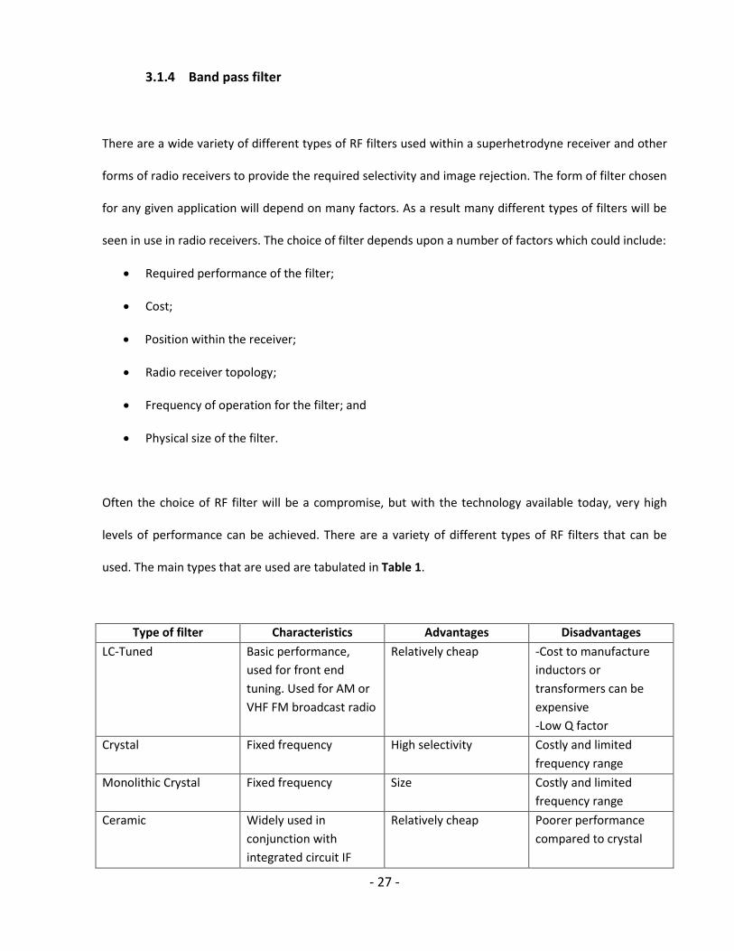
used. The main types that are used are tabulated in Table 1.
Type of filter Characteristics Advantages Disadvantages
LC-Tuned Basic performance,
used for front end
tuning. Used for AM or
VHF FM broadcast radio
Relatively cheap -Cost to manufacture
inductors or
transformers can be
expensive
-Low Q factor
Crystal Fixed frequency High selectivity Costly and limited
frequency range
Monolithic Crystal Fixed frequency Size Costly and limited
frequency range
Ceramic Widely used in
conjunction with
integrated circuit IF
Relatively cheap Poorer performance
compared to crystal

- 28 -
strips for commercial
broadcast receivers and
televisions.
Microstrip Mostly used at
frequencies above VHF
and microwave
Cost effective Difficult to tune
Mechanical Generally used in older
systems
High selectivity, easy to
tune
-Size and tendency to
drift
-Expensive to
manufacture
Surface Acoustic Wave
(SAW)
Widely used in cell
phone applications.
Cost effective and good
performance
Limited frequency range
Table 1 Comparison of filter types available
The main purpose of the bandpass filter before the mixer is to reject any unwanted signal frequencies.
For this receiver it was decided that a microstrip coupled line filter would be implemented.
This work describes the design of two coupled line filters in detail, using a different number of microstrip
sections for each. A comparison between the two designs of the bandpass filter before the mixer is
given.
3.1.5 Mixer and local oscillator
The purpose of the mixer is to convert the RF signal to an intermediate frequency (IF). This is done for
several reasons. Firstly, it is more difficult to construct good amplifiers, filters, and other components for
high RF frequencies (although this is getting easier with new technologies). Secondly, if all the amplifying
is done at the received frequency there is a possibility that some of the amplified signal will feed back
into the frontend and cause instability. The mixer multiplies the signal from the local oscillator with the
signal from the RF amplifier (input signal) in the time domain and produces the sum and difference

- 29 -
frequencies. The lower of the two output frequencies is selected as the IF by passing the mixer output
through a filter after the IF amplifier.
3.1.6 IF filter
The main purpose of the IF filter is to pass the wanted IF signal and reject any other mixing products as
well as the local oscillator feedthrough from the mixer. For this radio telescope a bandpass filter was
used to obtain the optimum rejection of unwanted signals.
3.1.7 IF amplifier
The intermediate frequency (IF) amplifier amplifies the output of the mixer. There are a number of
common IF frequencies, for example 45, 21.4 and 10.7 MHz, however there is no restriction to these
frequencies. The receiver for this research uses an IF frequency of 152 MHz.
3.1.8 Square law detector
The square law detector of a radio telescope is used to determine the RF power delivered to a load.
Square law implies that the dc component of the diode output is proportional to the square of the RF
input voltage. For the detector an Agilent 8472B detector was selected. This is a high performance Low
Barrier Schottky Diode Detector (LBSD) that is widely used for CW and pulsed power detection and
frequency response testing [Annexure 1]. These detectors do not require a dc bias thus their simplicity of
operation and excellent broadband performance make them useful measurement accessories. Schottky

- 30 -
diode detectors are typically used to detect small signals close to the noise level and to monitor large
signals well above the noise [4].
Figure 10 shows the comparison in diode response between a typical Schottky diode and that of a LBSD
detector [Annexure 1].
Figure 10 Comparison in diode response
3.1.9 Integrator and DC amplifier
The integrator following the detector is used to smooth out the small, rapid variations in the signal. The
integrator is driven by a source of very low impedance to have a reliable time constant. The system noise
temperature can be reduced, in theory, to any desired extent by increasing the integration time (after
detection), increasing the pre-detection bandwidth, or by taking the average of more than one
observation. In practice, however, the integration time cannot be increased beyond the point where it
begins to distort a true source profile, and the bandwidth cannot be made too wide without loss of
spectral information or introduction of interfering radio signals of terrestrial origin [17].

- 31 -
The DC amplifier is used to amplifier the signal from the integrator to an adequate level that is required
for the input to the ADC. Proper selection of the amplifier that drives an ADC is critical. The designer
must compare issues such as amplifier noise, bandwidth, settling time, and slew rate to the ADC’s signal-
to-noise ratio (SNR), spurious-free dynamic range (SFDR), input impedance, and sampling time [7].
3.1.10 Analogue to Digital converter
Since all the final processing of a radio telescope output is done with a computer, the analog voltage
from the output of the DC amplifier needs to be converted to digital.
3.2 System level calculations
The receiver bandwidth is determined from Equations 2.5 and 2.6, for KR=1 and n=1
√ [ ]
And from Equation 2.7
[ ] [ ]
[ ] [ ]
For a 5 m parabolic reflector, assuming η = 0.5
[ ]

- 32 -
A minimum sensitivity for the telescope was specified as 100 Jy. This was based on the high level of
baseline noise expected due to the urban location of the instrument.
Thus for ∆Smin = 100 Jy
[ ]( )
With t = 0.01 s and assuming that the sky noise temperature is approximately equal to TR [17], for a
receiver noise figure of 1 dB, F = 1.26 and TR = 75.4 K.
Then from Equation 3.1
√
It was decided to design the receiver bandwidth to four times the minimum, as it was assumed that the
sky noise temperature (TSKY) would probably be significantly higher than Tsys due to thermal radiation
from the two tower blocks into the antenna (refer to Figure 12). Hence a bandwidth of 80 MHz was
decided upon.
The required receiver gain is determined by looking at what the minimum input power required for the
detector. With reference to Figure 11, for the Agilent 8472B detector this is -45 dBm (square law
loaded).
So for a bandwidth of 80 MHz (set by the BPF and IF filter),

- 33 -
Noise floor of the receiver ( ) [dB]
( )
The total receiver gain required = -45 dBm – (-94 dBm) = 49 dB.
Assuming a total front end gain of approximately 20 dB, the minimum IF gain required = 49 dB – 20 dB =
29 dB or 2 IF amplifiers, with a nominal gain of approximately 15 dB each.
The DC amplifier gain is determined by looking at the input voltage specifications of the ADC. A MAXIM
186 ADC IC the input voltage range is 0 to 4.096 V with a resolution of 1 mV. The circuit design that was
used is available from the Radio Sky website [30]. It is the recommended circuit to be used for the
associated data logging software Radio Sykpipe II [30].
With reference to Figure 11, an input level of -45 dBm to the detector will give an output of 0.005 mV.
The minimum voltage gain required for the DC amplifier is thus
.
The maximum input voltage to the DC amplifier is
.
This corresponds to a maximum detector output of approximately -12 dBm, which is in the linear region
of the detector transfer characteristic curve.
This gives a dynamic range for the detector of -12 dBm – (-45 dBm) = 33 dB.

- 34 -
Figure 11 Typical Square Law Response of detector

- 35 -
CHAPTER 4 – DESIGN OF THE RECEIVER
4.1 Location of the telescope
The radio telescope uses a 5 m diameter parabolic reflector antenna which is mounted on a concrete
support beam on Level 0, running between two 5 level tower blocks on the Steve Biko Campus of the
Durban University of Technology as shown in Figure 12.
The tower blocks are orientated at 17.52 ° NE. The antenna has no azimuth control. Automatic
adjustment of the elevation is provided, allowing the antenna a variation of 26 ° from the zenith.
Effectively the azimuth of the antenna is thus fixed at either 17.52 ° or 197.52 °.
Figure 12 Location of the antenna
The two reasons for locating the antenna between the two tower blocks were:
1. Cost reduction; and
2. Interference rejection (refer to point 2 of pg 19).
Tower Block
1
Tower Block
2
- 36 -
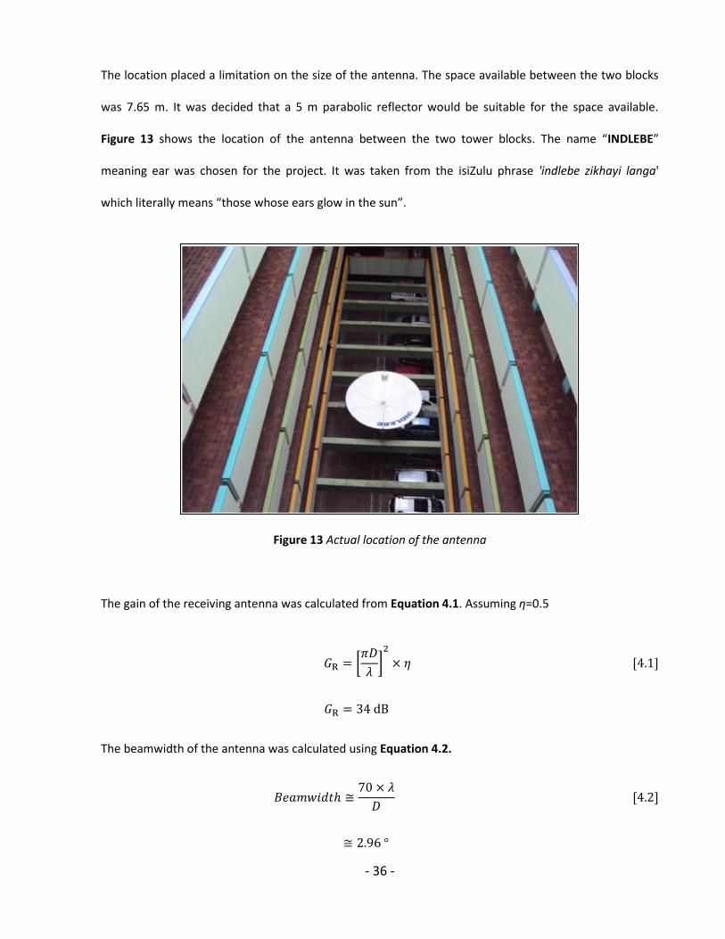
The location placed a limitation on the size of the antenna. The space available between the two blocks
was 7.65 m. It was decided that a 5 m parabolic reflector would be suitable for the space available.
Figure 13 shows the location of the antenna between the two tower blocks. The name “INDLEBE”
meaning ear was chosen for the project. It was taken from the isiZulu phrase 'indlebe zikhayi langa'
which literally means “those whose ears glow in the sun”.
Figure 13 Actual location of the antenna
The gain of the receiving antenna was calculated from Equation 4.1. Assuming η=0.5
[
]
[ ]
The beamwidth of the antenna was calculated using Equation 4.2.
[ ]

- 37 -
4.2 Design of the antenna
The parabolic antenna needed to be designed for maximum efficiency. In order to achieve efficiency
close to 100 %, it is necessary to provide illumination over the entire surface of the parabola. The
radiating source needs to be positioned at the focal point of the parabola. This means that there should
be equal power flux density over every unit area of the parabolic surface, but no power flux at the
extreme outer surface (edge) of the dish. This is impossible to achieve with a practical feed mechanism
[38].
The consequence of illuminating more than the extreme outer surface area is that some energy will ‘spill
over’ the edge and excessive side lobes will appear in the polar diagram, causing unwanted responses
not under the control of the operator, and a loss of gain to occur. A further potential loss of gain is the
surface accuracy of the parabola. If the deviation from a perfect parabola exceeds a certain amount (≈10
% of the wavelength), the loss of gain starts to become considerable, and this limits the maximum
frequency at which the parabola can produce adequate gain.
Another compromising factor is the choice of the focal length. In a parabolic reflector antenna the ratio
of focal length to diameter is known as the f/D ratio, and is the ratio of the distance of the focal point
from the centre of the parabola to the diameter. Typical terrestrial communication parabolic antennas
use f/D ratios of between 0.6 and 0.8 but the parabolas are very shallow. There are essentially three
important factors to consider when deciding on the focal length. These are:
1. Screening of the feed point from noise sources from the side. In a deep dish (short f/D ratio), the
feed can be positioned at or just below the edge of the parabola. This provides additional
attenuation of noise sources from the earth, which often are many times stronger than the

- 38 -
object under observation. When the feed is positioned in the plane of the lip (f/D ratio of 0.25),
this is known as a focal-plane system.
2. Mechanical problems of leverage of the feed supporting structure on the parabola. If the focal
point is positioned at a large f/D ratio, this can be considerable. This problem can cause severe
deformation of the parabolic surface as the antenna is declined from the zenith towards the
horizon. Another problem is that the supporting structure causes some obscuring of the surface
(aperture blocking).
3. The cable run required in a long f/D ratio, which can cause a degradation of the system noise
figure. The LNA is usually positioned directly at the feed point of the antenna and the length of
co-axial cable is very short.
Figure 14 shows the profile of the parabolic reflector for four different f/D ratios. The curves show the
profile of the parabolic reflector for the different f/D ratios. For the Indlebe radio telescope it was
decided that a parabolic reflector with an f/D ratio of 0.5 be selected with the corresponding focal point
being at 2.5 m above the base of the reflector. This was the ideal selection because of the location of the
dish. The proposed design of the feedhorn (ref. to Section 4.4) was such that the feedhorn could be
lowered to the one side of one of the tower blocks so that the feedhorn front end electronics could be
easily accessed.

- 39 -
Figure 14 Profile of the reflector for different f/D ratios
4.3 Manufacture of the antenna
The dish was manufactured by the Technology Station Prototyping Unit which is part of the Mechanical
Engineering Department at the DUT. The complete dish is made up of 8 equal petals. The (female)
tooling used in the manufacture of each petal was machined from low-cost polystyrene and over coated
with a thin layer of Glass Reinforced Plastic (GRP) as a durable moulding surface. This was sealed with
filler, medium solid (MS) filling primer and 2 k enamel paint which included a hardener. This was
polished to a high gloss in the interests of a good surface finish for each petal. Figure 15 shows one of
the layers being placed into the polystyrene mould.
0.00
0.50
1.00
1.50
2.00
2.50
3.00
3.50
Heig
ht
(m)
Diameter (m)
Parabolic Reflector
F/D=0.6
F/D=0.4
F/D=0.3
F/D = 0.5

- 40 -
Figure 15 One petal of the dish being manufactured
Figure 16 shows a cross sectional view of the layup of each of the 8 identical petals.
Figure 16 Cross sectional view of each petal
The layup of each of the 8 identical petals was as follows:
The first coat to go down effectively became the outermost surface. This therefore had to be
proven in terms of ultra violet (UV) stability, as well as having a suitably high glass transition
temperature (the temperature at which it begins to lose its rigidity). An epoxy gel coat system
was selected, but it’s very low viscosity meant that the standard saline based release system
Gelcoat – NCS 64
Conductive mesh - 2 mm pitch
Glass fibre cloth – 290 g/m2
Coremat Xi 3 – 3 mm
P1075Glass fibre cloth – 290 g/m2

- 41 -
could not be used. A Teflon based wax system was selected due to its low surface energy,
allowing the use of low viscosity gel coats.
This was allowed to partially cure before a layer of 290 gm-2 glass fabric was laid down and wet
out with epoxy resin. Aluminium mesh with a 2 mm pitch was laid down on top of this and the
entire laminate was compacted overnight by a vacuum bag, pulling down at 80 kPa. In order to
speed up the cure time, the room was heated to 35 ⁰C.
The bag was then removed and the surface abraded. A layer of 3 mm thick core-mat was laid
onto the mesh and this was covered by another layer of 290 gm-2 glass fabric. The laminate was
bagged again and cured at an elevated temperature.
The surface of each petal was then finally abraded, sprayed with MS primer and painted matt
white with 2 k enamel. Once the petals were manufactured, the Technology Station Prototyping
Unit did a tooling accuracy analysis on one of the petals. This is shown in Figure 17. As can be
seen there is very good correlation between Y target and Y achieved. Figure 18 shows an
expanded view of the tooling accuracy measurement. The graph indicates that the accuracy of
the petal is better than 1 mm.
Figure 17 Tooling accuracy of one petal

- 42 -
Figure 18 Expanded view of the tooling accuracy measurement
4.4 Design of the feedhorn
There are several options for a feedhorn for a parabolic reflector [8]. These are shown in Figure 19 [27].
The axial or front feed antenna configuration was selected due to the location of the antenna between
two tower blocks. The feedhorn is supported by two rigid aluminium arms that are attached to the
parabolic reflector such that it can be lowered or raised to one side of one of the tower blocks. The
necessary signal cables are run inside one of the support arms.
Figure 19 Feedhorn placement options
- 43 -
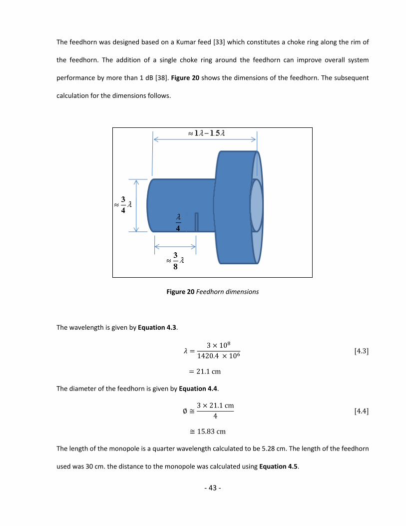
The feedhorn was designed based on a Kumar feed [33] which constitutes a choke ring along the rim of
the feedhorn. The addition of a single choke ring around the feedhorn can improve overall system
performance by more than 1 dB [38]. Figure 20 shows the dimensions of the feedhorn. The subsequent
calculation for the dimensions follows.
Figure 20 Feedhorn dimensions
The wavelength is given by Equation 4.3.
[ ]
The diameter of the feedhorn is given by Equation 4.4.
[ ]
The length of the monopole is a quarter wavelength calculated to be 5.28 cm. The length of the feedhorn
used was 30 cm. the distance to the monopole was calculated using Equation 4.5.

- 44 -
[ ]
The VSWR of the feedhorn was measured using an HP8753 Vector Network Analyser. The results are
shown in Figure 21. The VSWR was measured to be 2.046 at 1.42 GHz. The x-axis is measuring frequency
(100 MHz/div) and the y-axis is measuring the VSWR value which does not have a unit of measure as it is
a ratio. The monopole length required some tuning for the optimum result.
Figure 21 VSWR of the antenna
Figure 22 shows the mechanical drawing of the top and side view of the feedhorn. This was
manufactured by the Technology Station Prototyping Unit. The feedhorn was designed so that it could be

- 45 -
lowered or raised to obtain an accurate position of the focal point. Two brackets were attached to the
supporting arms and a sliding mechanism was employed. The feedhorn was adjusted so that the focal
point of the parabolic reflector falls slightly inside the mouth of the feedhorn. This can be determined by
using Equation 4.6 [33].
Figure 22 Mechanical view of the feedhorn
[ ]
where: a = distance the focus should be inside the feedhorn [cm]
D = diameter of the dish [cm]
d = diameter of the feedhorn (not of choke ring) [cm]
f = focal length of dish [cm]

- 46 -
Figure 23 clearly shows the feedhorn attached to the two supporting arms. The sliding mechanism can
be seen that is used to lower or raise the feedhorn to obtain the correct focal point.
Figure 23 The feedhorn attached to the two support arms
The LNA is connected directly to the monopole via a SMA barrel connector. The front end electronics are
mounted in a box above the feedhorn as shown in Figure 24. The entire feedhorn with electronics is
housed in a custom made cover that protects it from the environment. This can be seen in Figure 25
which shows the complete reflector with feedhorn installed.

- 47 -
Figure 24 Feedhorn with LNA and front-end electronics
Figure 25 Completed parabolic reflector with feedhorn
LNA
FRONT-END ELECTRONICS

- 48 -
4.5 Automation of the reflector
Essentially the dish is designed such that it is equally balanced around a pivot point. A 0.55 kW motor
and variable speed drive is sufficient as the power source for positioning the dish. The motor is mounted
on a rotating table and a worm screw is coupled directly to the motor shaft. A following nut on the worm
screw is fixed to the supporting framework of the dish. Simply driving the motor then moves the dish in
either direction. An absolute shaft encoder is mounted adjacent to the motor and coupled to the motor
with a toothed belt. The diameters of the two pulley wheels are identical meaning that the angular
rotation of the encoder and the motor will be the same.
Two feedback signals are used to measure the position of the dish. An inclinometer is mounted on the
framework supporting the dish and a shaft encoder is used on the motor output shaft. In addition to
providing the dish position these two signals can also be used for monitoring any flexion in the dish,
backlash, etc. The error signal generated is used to drive the motor via the variable speed drive.
Both hardware and software limits are implemented to prevent the dish from rotating too far. The
hardware limit switches control a relay that will interrupt the signals to the variable speed drive while
the software limit switches interrupt the signal from the microcontroller. A block diagram of the drive
control system is shown in Figure 26. The output signal from the microprocessor is fed to the control PC
which is running HyperTerminal to select the angle of elevation.
The design and construction of the drive control system was not included in the scope of this research
and will thus not be discussed further.

- 49 -
Figure 26 Block diagram of the drive control system
4.6 Design of the Low Noise Amplifier
The low noise amplifier or LNA as it is commonly referred to, is the most important stage of the receiver
in terms of determining the overall noise figure of the entire system. It is critical that the noise figure of
the first stage of any receiver be as low as possible. Other factors that needed to be considered were
values of Gain, Power requirement, Third Order Intercept Point (IP3) and cost. It was decided that a 5 V
DC supply would be used to power the entire front-end and this voltage would be fed up to the feedhorn
from a panel mounted in the basement level of one of the tower blocks.
Considering these factors, suitable devices had to be identified that can operate at low voltages and be
able to produce as low a noise figure as possible. Several devices were researched to determine which
one would be most suitable for the application and at a low cost. Table 2 is the list of devices that were

- 50 -
researched and their corresponding values of Gain, Noise figure, Power requirement, Third Order
Intercept Point (IP3) and cost.
Device Gain (dB) Noise Figure
(dB) Bias
IP3
(dBm) COST
ATF-10136
GaAsFET 14 0.4 2 V, 25 mA +20 $2.30
ATF-34143
PHEMPT 16 0.6 2 V, 20 mA +32 $3.50
ATF-33143
PHEMPT 18.46 0.4 4 V, 80 mA +34 $3.50
Minicircuits
ZRL-2400LN(+) 28 1.2 12 V +25 $140
SETI League HP
MGA-86576 25 <2 dB 5 V +16 $105
Table 2 Comparison of active device parameters
As the aim of this research was to develop a low cost radio telescope, the ATF-34143 PHEMPT and ATF-
10136 GaAsFET were the devices that were selected based on cost and availability. The Gain and Noise
Figure values were adequate and it was decided that two amplifiers would be designed and constructed
and their performance compared.
4.6.1 Initial LNA Design Using the ATF-34143 PHEMPT
Agilent Technologies ATF-34143 is a low noise PHEMPT designed for use in low cost commercial
applications in the VHF through 6 GHz range. The ATF-34143 is housed in a 4-lead SC-70 (SOT-343)
surface mount plastic package. The 800 micron gate width of the ATF-34143 makes it ideal for

- 51 -
applications in the VHF and lower GHz frequency range by providing low noise figure coincident with
high intercept point. The wide gate width also provides lower impedances that are easy to match [2].
The parameters of the active device that were used for the design, were extracted from the datasheet
[Annexure 2], and are shown in Table 3. This bias point was selected because both the S-parameters and
Noise Figure parameters were available from the manufacturers’ datasheet (Annexure 2, pg 119).
Operating Frequency 1420 MHz
Vdd +5 V
Vds +3 V
Ids 20 mA
VP +1.3 V
Idss 100 mA
Table 3 Parameters of the ATF-34143 PHEMPT
For this active device, parameters such as gain, noise figure, and linearity are controlled by the PHEMPT’s
bias point. So it is critical to bias the device properly. Both the gate and drain of a PHEMPT must meet
bias conditions to function properly. The drain voltage relative to the source (Vds) should be ≥ 2 V, while
the gate voltage relative to the source (Vgs) is used to set the current flow from the drain to the source
(Idd). With Vgs = 0 V and Vds ≥ 2 V, the FET is in its saturated state (Idss) and draws the maximum amount of
current. The value of Idss is determined by the overall geometry and size of the PHEMPT. Lowering Vgs to
approximately -0.7 V, the device enters its pinchoff state and turns off [34]. The enhancement mode
technology provides superior performance while allowing direct grounding of the transistor’s source
terminal. This greatly simplifies the power supply requirement as the entire amplifier can be powered
using a single polarity voltage supply [18].

- 52 -
For this design a self-biasing resistor is placed between the source of the device and ground. The source
is floated above ground when current flows through the resistor. The source resistor simplifies the bias
network design, but also slightly degrades the noise figure performance and the added source bypass
capacitor can cause instability. From the manufacturer’s datasheet, the gate source voltage required for
a drain current of 20 mA is -0.4 V (Annexure 2, Fig.1, pg 119). In order to supply -0.4 V for a drain current
of 20 mA the source and drain resistors are calculated as follows:
On the test bench the bias resistors were tuned to obtain the exact bias point of Vds = 3 V and Id = 20 mA.
The final resistor values used were Rs = 2 x 68 Ω in parallel i.e one on each source lead to ground, and Rd
= 100 Ω.
The Advanced Design System simulation program was used to interpolate the stability factor K at 1420
MHz. The stability factor was 0.552 which indicated that the device was potentially unstable. In order to
be able to use the device, it needs to be made unconditionally stable. One method of making the device
unconditionally stable is by adding additional resistance. The other method is by adding additional
source lead inductance, in which case the input return loss is improved as well as the stability. A

- 53 -
potential downside is reduced low frequency gain. However decreased gain also correlates to higher
intercept point. It is therefore critical to add just the right amount of additional source lead inductance
to ensure stability. Excessive source inductance will manifest itself in the form of high frequency gain
peaking [2].
The SOT-323 package has two source leads for the device so for the design it was decided to use 6 nH on
each lead of the device giving an equivalent source lead inductance of 3 nH. Figure 27 is an ADS
simulation of the active device with source lead inductance. An additional 390 Ω stabilizing resistor was
added in shunt with the drain of the device to improve the stability. Table 4 lists the interpolated results
at 1420 MHz. It is clear that the device is unconditionally stable as the Rollet Stability factor is greater
than 1.
Figure 27 ADS Simulation of the active device with 3 nH source lead inductance

- 54 -
Frequency 1420 MHz
Stability Factor K 1.127
NFmin [dB] 0.245
Γopt 0.658∟41.43 ⁰
Table 4 Interpolated values of active device with 3 nH source lead inductance
NFmin is a function of the device bias point and the operating frequency, and there is one value of Γopt
(optimum source reflection coefficient for minimum noise figure) associated with each value of NFmin
[30]. When designing for the lowest noise figure the source termination can be chosen to be Γopt,
provided that the device is unconditionally stable. A simple matching application was used to compute
the optimum input impedance matching circuit to match 50 Ω to Γopt*. Figure 28 shows the different
input matching options available. The first option was selected.
Figure 28 Options for the input impedance matching circuit

- 55 -
The circuit in Figure 29 includes the input matching circuit. The circuit was simulated to obtain a value of
S22 = 0.421∟-53.242.
Figure 29 ADS Simulation with input matching circuit
The output impedance matching circuit was determined by matching S22 to 50 Ω. The options for the
output impedance matching circuit are shown in Figure 30.
Figure 30 Options for the output impedance matching circuit

- 56 -
The first option was selected for the output match. Figure 31 shows the schematic with the input and
output matching circuits. The simulated response in Figure 32 indicates that the input and output return
losses are greater than 19 dB. The expected gain of the circuit is 10.37 dB and the noise figure is 0.245
dB.
Figure 31 Circuit simulation including input and output matching circuits
Figure 32 Gain and noise figure values with input and output impedance match
1.2 1.4 1.6 1.81.0 2.0
-40
-30
-20
-10
-50
0
freq, GHz
dB
(S(1
,1))
Readout
m1
dB
(S(2
,2))
Readout
m2
m1freq=dB(S(1,1))=-19.659
1.420GHzm2freq=dB(S(2,2))=-39.755
1.420GHz
1.2 1.4 1.6 1.81.0 2.0
2
4
6
8
10
0
12
freq, GHz
dB
(S(2
,1))
Readout
m3
nf(
2)
Readout
m4
m3freq=dB(S(2,1))=10.366
1.412GHzm4freq=nf(2)=0.245
1.420GHz

- 57 -
Figure 33 shows the complete amplifier circuit that was simulated on ADS. It includes all bias resistors
and impedance matching networks. This simple biasing technique is very desirable since it reduces the
overall parts count. The source resistor must be decoupled, using a low-impedance capacitor at the
desired operating frequency. Since the device has two source leads, each lead has a resistor and
capacitor that was grounded.
Figure 33 Final circuit simulation using the ATF-34143 PHEMPT
Figure 34 shows the simulated response of the LNA. The S21 = 10.367 dB and the NF = 0.245 dB. The
input and output return loss values are better than 20 dB.
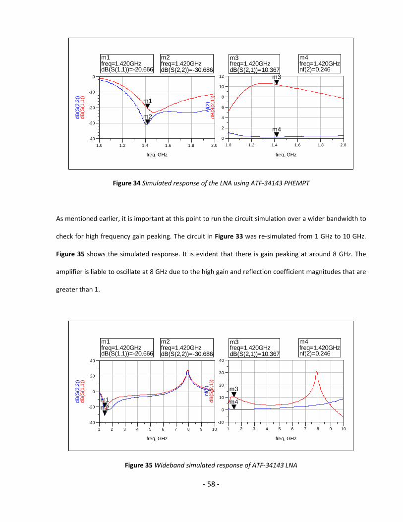
- 58 -
Figure 34 Simulated response of the LNA using ATF-34143 PHEMPT
As mentioned earlier, it is important at this point to run the circuit simulation over a wider bandwidth to
check for high frequency gain peaking. The circuit in Figure 33 was re-simulated from 1 GHz to 10 GHz.
Figure 35 shows the simulated response. It is evident that there is gain peaking at around 8 GHz. The
amplifier is liable to oscillate at 8 GHz due to the high gain and reflection coefficient magnitudes that are
greater than 1.
Figure 35 Wideband simulated response of ATF-34143 LNA
1.2 1.4 1.6 1.81.0 2.0
-30
-20
-10
-40
0
freq, GHz
dB
(S(1
,1))
Readout
m1
dB
(S(2
,2))
Readout
m2
m1freq=dB(S(1,1))=-20.666
1.420GHzm2freq=dB(S(2,2))=-30.686
1.420GHz
1.2 1.4 1.6 1.81.0 2.0
2
4
6
8
10
0
12
freq, GHz
dB
(S(2
,1))
Readout
m3
nf(
2)
Readout
m4
m3freq=dB(S(2,1))=10.367
1.420GHzm4freq=nf(2)=0.246
1.420GHz
2 3 4 5 6 7 8 91 10
-20
0
20
-40
40
freq, GHz
dB
(S(1
,1))
Readout
m1dB
(S(2
,2))
Readout
m2
m1freq=dB(S(1,1))=-20.666
1.420GHzm2freq=dB(S(2,2))=-30.686
1.420GHz
2 3 4 5 6 7 8 91 10
0
10
20
30
-10
40
freq, GHz
dB
(S(2
,1))
Readout
m3
nf(
2)
Readout
m4
m3freq=dB(S(2,1))=10.367
1.420GHzm4freq=nf(2)=0.246
1.420GHz

- 59 -
According to Agilent [1], to reduce high frequency gain peaking for this device, the source lead
inductance needs to be reduced. The source lead inductance was reduced to 1.5 nH and the circuit in
Figure 36 was re-simulated.
Figure 36 Re-simulated LNA circuit with 1.5 nH source lead inductance
Figure 37 shows the wideband response with 1.5 nH source lead inductance. The high frequency gain
peaking is still evident. The source lead inductance was reduced further to 0.5 nH.
Figure 37 Wideband response of ATF-34143 LNA with 1.5 nH source lead inductance
2 3 4 5 6 7 8 91 10
-30
-20
-10
0
-40
10
freq, GHz
dB
(S(1
,1))
Readout
m1
dB
(S(2
,2))
Readout
m2
m1freq=dB(S(1,1))=-8.412
1.420GHzm2freq=dB(S(2,2))=-11.479
1.420GHz
2 3 4 5 6 7 8 91 10
5
10
0
15
freq, GHz
dB
(S(2
,1))
Readout
m3
nf(
2)
Readout
m4
m3freq=dB(S(2,1))=12.526
1.420GHzm4freq=nf(2)=0.184
1.420GHz

- 60 -
The circuit shown in Figure 38 includes the 0.5 nH source lead inductance.
Figure 38 Re-simulated LNA circuit with 0.5 nH source lead inductance
Figure 39 shows the wideband response of the LNA using 0.5 nH source lead inductance. There is no
further gain peaking at around 8 GHz. However the output return loss graph indicates that the match to
50 Ω is no longer existent. To correct this, the output matching circuit was redesigned. So the initial
circuit in Figure 29 was re-simulated with 0.5 nH of source lead inductance. The new value of S22 was
used to design a conjugate match at the output to 50 Ω.
Figure 39 Wideband response of ATF-34143 LNA with 0.5 nH source lead inductance
2 3 4 5 6 7 8 91 10
-20
-15
-10
-5
0
-25
5
freq, GHz
dB
(S(1
,1))
Readout
m1
dB
(S(2
,2))
Readout
m2
m1freq=dB(S(1,1))=-2.343
1.420GHzm2freq=dB(S(2,2))=-5.529
1.420GHz
2 3 4 5 6 7 8 91 10
5
10
15
20
25
0
30
freq, GHz
dB
(S(2
,1))
Readout
m3
nf(
2)
Readout
m4
m3freq=dB(S(2,1))=14.077
1.420GHzm4freq=nf(2)=0.164
1.420GHz

- 61 -
Figure 40 is the circuit that was re-simulated to get a new S22 value of 0.335∟-134.966. The output
impedance matching circuit was implemented by matching S22 to 50 Ω. The options for the output
impedance matching circuit are shown in Figure 41.
Figure 40 ADS Simulation with input matching circuit and 0.5 nH source lead inductance
Figure 41 Options for the new output impedance matching circuit

- 62 -
Option 1 was selected and the final LNA circuit in Figure 42 was re-simulated with the bias resistors.
Capacitor values were changed to E12 and L4 and L5 were tuned for optimum noise figure.
Figure 42 Final LNA circuit with 0.5 nH source lead inductance
The final LNA circuit response is shown in Figure 43. At 1.42 GHz the gain is 16.14 dB and the noise figure
is 0.19 dB. The input return loss is 5.34 dB and the output return loss is 13.94 dB.
Figure 43 Final LNA circuit response
1.2 1.4 1.6 1.81.0 2.0
-20
-15
-10
-5
-25
0
freq, GHz
dB
(S(1
,1))
Readout
m1
dB
(S(2
,2))
Readout
m2
m1freq=dB(S(1,1))=-5.343
1.420GHzm2freq=dB(S(2,2))=-13.939
1.420GHz
1.2 1.4 1.6 1.81.0 2.0
5
10
15
0
20
freq, GHz
dB
(S(2
,1))
1.284G16.19
m3
nf(
2)
Readout
m4
m3freq=dB(S(2,1))=16.141
1.284GHzm4freq=nf(2)=0.194
1.420GHz

- 63 -
The actual measured response (Figure 44) after the amplifier was constructed was measured using a
Vector Network Analyzer. The gain was measured to be 15.915 dB and the input and output return loss
values are +2.8 dB and +11.7 dB respectively at 1420 MHz.
Figure 44 Measured response of the LNA using ATF-34143 PHEMPT
To obtain an accurate measurement of the noise figure of the LNA, a Spectrum Analyzer was configured
for noise figure measurement. Figure 45 shows the measured response. The gain is 15.16 dB and the
noise figure is 0.58 dB. It should be noted that the noise figure is higher than what is specified in the
datasheet for this device. This is due to the addition of circuit parasitic inductances resulting from the
lead lengths of components in the final circuit implementation.

- 64 -
Figure 45 Gain and Noise Figure measurement of LNA using ATF-34143 PHEMPT
The printed circuit board layout was designed using Advanced Design System. Track lengths and lead
lengths were kept to a minimum to avoid adding additional inductance. The tuning of the source lead
inductance proved to be critical. Two capacitors were connected to each source lead to ground. To
adjust the source lead inductance, the capacitor was either soldered closer to or further away from the
source lead. Careful consideration was taken to orient the inductors at right angles to each other so as to
avoid coupling between them.
In some instances, the enclosure can cause undesirable feedback across the circuit board which can
cause instabilities. This phenomenon is true of any amplifier design [12]. A cross sectional view of the
housing can be viewed as a piece of waveguide whose dimensions, both width and height, determine the
band of frequencies that it may pass with minimal attenuation. A combination of the amplifier response
along with the housing response could contribute to instabilities if not controlled. The use of low profile
surface mount components will minimize this effect. It is preferred that the cover is at least 0.3 to 0.5
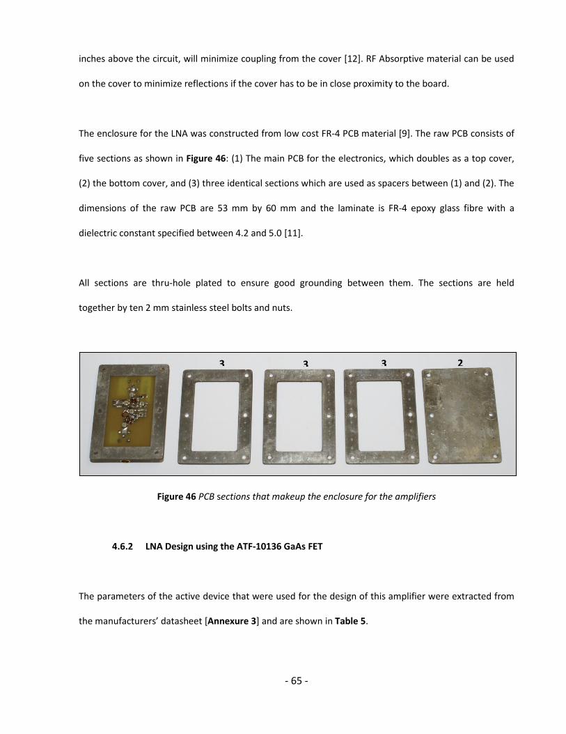
- 65 -
inches above the circuit, will minimize coupling from the cover [12]. RF Absorptive material can be used
on the cover to minimize reflections if the cover has to be in close proximity to the board.
The enclosure for the LNA was constructed from low cost FR-4 PCB material [9]. The raw PCB consists of
five sections as shown in Figure 46: (1) The main PCB for the electronics, which doubles as a top cover,
(2) the bottom cover, and (3) three identical sections which are used as spacers between (1) and (2). The
dimensions of the raw PCB are 53 mm by 60 mm and the laminate is FR-4 epoxy glass fibre with a
dielectric constant specified between 4.2 and 5.0 [11].
All sections are thru-hole plated to ensure good grounding between them. The sections are held
together by ten 2 mm stainless steel bolts and nuts.
Figure 46 PCB sections that makeup the enclosure for the amplifiers
4.6.2 LNA Design using the ATF-10136 GaAs FET
The parameters of the active device that were used for the design of this amplifier were extracted from
the manufacturers’ datasheet [Annexure 3] and are shown in Table 5.
2
Figure
34
Sections
that
makeu
333

- 66 -
Operating Frequency 1420 MHz
Vdd +5 V
Vds +2 V
Id 25 mA
Vp +1.3V
Idss 130 mA
Table 5 Parameters of the ATF-10136 GaAs FET
A self bias circuit was again used to keep the number of components to a minimum. For a Vds of 2 V and
an Id of 25 mA, the values of Rs and Rd were found to be 27 Ω and 390 Ω respectively.
The Advanced Design System simulation program was used to firstly interpolate the stability factor K at
1420 MHz. The stability factor was 0.552 which indicated that the device was potentially unstable.
A 47 Ω resistor in shunt with the drain was added and a source lead inductance of 1 nH was added to
improve the stability factor. Figure 47 shows the ADS circuit that was simulated.
Figure 47 ADS simulation using ATF-10136 GaAs FET

- 67 -
Table 6 shows the parameters that were used for the design of the input impedance matching circuit.
The stability factor has increased to 2.472 indicating that the device is unconditionally stable.
Frequency 1420 MHz
Stability Factor K 2.472
NFmin [dB] 0.633
Γopt 0.771∟32.608 ⁰
Table 6 Design parameters used for designing the input matching circuit
Figure 48 shows the input matching network options to match Γopt* to 50 Ω.
Figure 48 Options for the input matching network
The L-match with a capacitor of 0.91 pF and inductor of 8.83 nH were chosen and the circuit in Figure 49
was re-simulated to get the value of S22 = 0.276∟-148.621.

- 68 -
Figure 49 Simulation with the input impedance matching circuit
The output impedance matching circuit was implemented by matching S22 to 50 Ω. The options for the
output impedance matching circuit are shown in Figure 50.
Figure 50 Options for the output matching circuit

- 69 -
The first option was selected and values set to standard. The circuit with input and output matching
networks is shown in Figure 51.
Figure 51Circuit simulation with input and output impedance matching networks
The response of the amplifier (Figure 52) at 1420 MHz confirms that the input and output return loss is
good. The S21 value is 10.57 dB and the noise figure is 0.66 dB.
Figure 52 Simulated response with input and output impedance networks
1.2 1.4 1.6 1.81.0 2.0
-30
-20
-10
-40
0
freq, GHz
dB
(S(1
,1))
Readout
m1
dB
(S(2
,2))
Readout
m2
m1freq=dB(S(1,1))=-18.501
1.420GHzm2freq=dB(S(2,2))=-29.889
1.420GHz
1.2 1.4 1.6 1.81.0 2.0
2
4
6
8
10
0
12
freq, GHz
dB
(S(2
,1))
Readout
m3
nf(
2)
Readout
m4
m3freq=dB(S(2,1))=10.571
1.420GHzm4freq=nf(2)=0.663
1.420GHz

- 70 -
The bias resistors were added to the circuit in Figure 53 with the impedance matching circuits and
simulated.
Figure 53 ADS circuit simulation of ATF-10136 LNA
The simulated response in Figure 54 indicates that a gain of 10.67 dB and a NF of 0.66 dB should be
achieved.
Figure 54 Simulated response of ATF-10136 LNA
1.2 1.4 1.6 1.81.0 2.0
-30
-20
-10
-40
0
freq, GHz
dB
(S(1
,1))
Readout
m3
dB
(S(2
,2))
Readout
m4
m3freq=dB(S(1,1))=-17.023
1.420GHzm4freq=dB(S(2,2))=-22.878
1.420GHz
1.2 1.4 1.6 1.81.0 2.0
2
4
6
8
10
0
12
freq, GHz
dB
(S(2
,1))
Readout
m1
nf(
2)
Readout
m2
m1freq=dB(S(2,1))=10.669
1.420GHzm2freq=nf(2)=0.663
1.420GHz

- 71 -
The circuit in Figure 53 was simulated over a wider bandwidth to check for high frequency gain peaking.
Figure 55 shows the wideband response. It is evident that the gain is peaking around 9 GHz and the input
reflection coefficient magnitude is greater than 1.
Figure 55 Wideband response of ATF-10136 LNA
The source lead inductance was reduced to eliminate the high frequency gain peaking. The gate inductor
which forms part of the input matching circuit proved to be critical and was tuned to obtain minimum
noise figure at the design frequency. A final source lead inductance of 0.1 nH was used and the gate
inductor was changed to 8 nH as shown in Figure 56.
Figure 56 Final optimized LNA circuit using ATF-10136 GaAs FET
2 3 4 5 6 7 8 91 10
-30
-20
-10
0
-40
10
freq, GHz
dB
(S(1
,1))
Readout
m3
dB
(S(2
,2))
Readout
m4
m3freq=dB(S(1,1))=-17.023
1.420GHzm4freq=dB(S(2,2))=-22.878
1.420GHz
2 3 4 5 6 7 8 91 10
2
4
6
8
10
0
12
freq, GHz
dB
(S(2
,1))
Readout
m1
nf(
2)
Readout
m2
m1freq=dB(S(2,1))=10.669
1.420GHzm2freq=nf(2)=0.663
1.420GHz

- 72 -
The final simulated response of the amplifier can be seen in Figure 57. The gain is 15.94 dB and the noise
figure is 0.49 dB. Both the input and output return losses are acceptable and there is no high frequency
gain peaking at 9 GHz.
Figure 57 Final simulated response of LNA using ATF-10136 GaAsFET
The printed circuit board layout was designed using ADS software. Two 50 Ω transmission lines of 1.88
mm width were included between the input and output connectors to ensure that the active device
remains central to the PCB. Figure 58 shows the final constructed circuit including the 50 Ω transmission
lines at the input and output of the amplifier. The same method that was used for the enclosure of the
ATF-34143 LNA was used for this amplifier.
Figure 58 Final constructed amplifier circuit using ATF-10136 GaAs FET
2 3 4 5 6 7 8 91 10
-15
-10
-5
-20
0
freq, GHz
dB
(S(1
,1))
Readout
m3
dB
(S(2
,2))
Readout
m4
m3freq=dB(S(1,1))=-3.585
1.420GHzm4freq=dB(S(2,2))=-13.984
1.420GHz
2 3 4 5 6 7 8 91 10
0
5
10
15
-5
20
freq, GHz
dB
(S(2
,1))
Readout
m1
nf(
2)
Readout
m2
m1freq=dB(S(2,1))=15.939
1.420GHzm2freq=nf(2)=0.493
1.420GHz

- 73 -
The final measured response can be seen in Figure 59. The input return loss, S11 is 19.3 dB and the
output return loss, S22 is 2.5 dB. The noise figure of this LNA was measured to be 0.98 dB [Figure 60] and
the gain was measured to be 15.52 dB.
Figure 59 Final measured response of LNA using ATF-10136 GaAs FET
Figure 60 Gain and Noise Figure measurement of LNA using ATF-10136 GaAsFET

- 74 -
4.6.3 Comparison of the Low Noise Amplifiers
Table 7 shows a comparison of the measured values of the two amplifiers that were designed.
DEVICE TYPE GAIN (dB) Noise Figure (dB) S11 (dB) S22 (dB)
ATF-34143 15.16 0.58 -2.84 -11.73
ATF-10136 15.52 0.98 -2.54 -19.30
Table 7 Comparison of measured values for the two amplifiers
Both amplifiers performed well when connected to the VNA but when connected to the antenna the
ATF-34143 amplifier was oscillating. This was because the output impedance of the antenna is not
exactly 50 Ω. The ATF-10136 amplifier was stable when connected to the antenna. Although the NF is
higher than the ATF-34143 amplifier, stability is more important. The ATF-10136 amplifier was used as
the LNA for this radio telescope. S11 is the input reflection coefficient and S22 is the output reflection
coefficient.
4.7 Radio Frequency amplifier design
It was decided that a separate RF amplifier would not be designed. Figure 61 shows the new front-end
line up of the receiver where the LNA is the ATF-10136 amplifier circuit described in section 4.6.2 and the
RFA is the ATF-34143 circuit described in section 4.6.1. The 3 dB pad between the LNA and RFA was
necessary to ensure overall stability of the front end. An Agilent 8761A RF switch was used for the noise
calibration measurement of the receiver. Its insertion loss is less than 0.1 dB at 1420 MHz which is
negligible and is therefore not included in the cascaded gain calculation of the front end.

- 75 -
Figure 61 New front-end line-up due to instability
Using Friis’s formula [20] to calculate the overall gain and noise figure of the front end yields:
( )
( )
( )
( )
The total cascaded gain

- 76 -
4.8 Cascaded gain and noise figure measurement
A cascaded gain and noise figure measurement of the frontend amplifiers is shown in Figure 62. The
results indicate a gain of 30.82 dB and a noise figure of 1.02 dB. The difference between the calculated
and measured cascaded gain of the frontend amplifiers can be attributed to the inclusion of a cable
between the LNA and the 3 dB PAD. This was included in the final hardware implementation due to the
space constraints within the feedhorn enclosure.
Figure 62 Cascaded gain and noise figure plot of front end amplifiers
4.9 The band pass filter
The main purpose of the front end filter after the first two stages of amplification were to attenuate
unwanted signals and allow the 1420 MHz signal to be fed into the mixer and be down-converted to the
IF. A coupled line Chebyshev band pass filter was selected for the design (refer to Table 1, pg 27). The

- 77 -
bandwidth of the filter was limited to 80 MHz. Two filters were designed using ADS software and the
response compared. Both filters were manufactured using a PCB router for better precision. Both filters
required some tuning to obtain the optimum response.
The ADS simulation shown in Figure 63 uses the Filter Design Guide while selecting the pass band and
stop band frequencies for a 3 dB bandwidth of 80 MHz and a stop band attenuation of 30 dB. The ADS
simulator presents a filter design with four microstrip sections as shown in Figure 64.
Figure 63 ADS Simulation of CL Filter 1
Figure 64 Microstrip sections of the CL Filter 1

- 78 -
Figure 65 shows the simulated filter response showing that an insertion loss of 1.029 dB is possible. The
3 dB bandwidth is 85 MHz and the attenuation in the stop band is greater than 33 dB.
Figure 65 Simulated response of the CL Filter 1
The PCB artwork was generated using ADS. Figure 66 illustrates the layout with the microstrip sections.
Figure 66 PCB artwork generated in ADS Layout
1.2 1.4 1.6 1.81.0 2.0
-60
-40
-20
-80
0
freq, GHz
dB
(S(2
,1))
Readout
m1
1.380G-4.102
m2
1.465G-3.965
m3
Readout
m4
1.630G-38.09
m5
m1freq=dB(S(2,1))=-1.029
1.420GHz
m2freq=dB(S(2,1))=-4.102
1.380GHzm3freq=dB(S(2,1))=-3.965
1.465GHz
m4freq=dB(S(2,1))=-33.386
1.280GHzm5freq=dB(S(2,1))=-38.092
1.630GHz

- 79 -
The Filter 1 PCB was manufactured using the LPKF PCB Router to ensure that the filter microstrip
sections are as accurate as possible. The complete filter (Figure 67) used SMA connectors for the input
and output ports. A minimal amount of tuning was required.
Figure 67 Actual PCB of Filter 1
The measured filter response is shown in Figure 68. The insertion loss is 2.9 dB at 1420 MHz and the 3 dB
bandwidth is 80 MHz. The difference between the simulated and measured insertion loss can be
attributed to slight inaccuracies of the transmission lines during the manufacturing process of the
printed circuit board. The stop band attenuation at 1280 MHz and 1630 MHz is greater than 35 dB.
Figure 68 Measured response of Filter 1

- 80 -
In the second filter design the number of microstrip sections, (N) were specified as three as highlighted
in Figure 69. The simulated response indicates that a lower insertion loss is obtainable but not as much
stop band attenuation as the first filter.
Figure 69 ADS Simulation of CL Filter 2 with three sections
It is evident that in Figure 70, there are only three microstrip sections compared to Filter 1 (Figure 64).
Figure 70 Microstrip sections of the CL Filter 2 with three sections

- 81 -
The simulated response (Figure 71) indicates that this filter has a better insertion loss of 0.6 dB and the 3
dB bandwidth is 84 MHz. The stop band attenuation is not as good as in Filter 1. It is only 22 dB.
Figure 71 Simulated response of the CL Filter 2 with three sections
The PCB layout was designed using ADS. Figure 72 reveals that the overall filter is much smaller due to it
having one less microstrip section.
Figure 72 PCB artwork generated in ADS Layout Filter 2
1.2 1.4 1.6 1.81.0 2.0
-40
-30
-20
-10
-50
0
f req, GHz
dB
(S(2
,1))
Readout
m1
Readout
m2
Readout
m3
Readout
m4
Readout
m5
m1freq=dB(S(2,1))=-0.592
1.420GHz
m2freq=dB(S(2,1))=-3.503
1.376GHzm3freq=dB(S(2,1))=-3.610
1.460GHz
m4freq=dB(S(2,1))=-22.133
1.280GHzm5freq=dB(S(2,1))=-25.618
1.630GHz

- 82 -
Filter 2 was also manufactured using the LPKF PCB router. Figure 73 shows the completed board.
Figure 73 Actual PCB design of Filter 2
The measured result of Filter 2 in Figure 74 has an insertion loss of 1.9 dB at 1420 MHz and a 3 dB
bandwidth of 70 MHz. The stop band attenuation at 1280 MHz and 1630 MHz is >26 dB.
Figure 74 Measured response of Filter 2

- 83 -
Figure 75 shows a comparison of the S21 plot from the VNA of both filters. It is clearly evident that Filter 2
has a better insertion loss whilst Filter 1 has a better stop band attenuation. The reason for this is that
Filter 1 has one more microstrip section. Consequently it resulted in a bigger filter than Filter 2. As space
on the front end was a critical factor it was decided that Filter 2 would be used.
Figure 75 Comparative plot of both filters
Figure 76 clearly shows the difference in size between the two filters.
Figure 76 Comparative size of both filters
Filter 1
Filter 2

- 84 -
4.10 Selection of IF components
Figure 77 is a block diagram of the IF stage of the receiver in more detail.
Figure 77 Block diagram of the IF stage
4.10.1 Mixer
The mixer down-converts the RF signal to the IF via a nonlinear mixing process. This nonlinearity
generates spurious products that are undesirable. The key concerns for the mixer are low spurious
products, low noise figure, conversion gain, low LO drive level, and low DC power consumption. Isolation
between the LO, RF and IF ports is also important. A Minicircuits ZEM-4300 mixer was used to convert
the 1420 MHz down to 152 MHz. The ZEM-4300 is a level 7 mixer operating from 300 MHz to 4300 MHz.
It has a low conversion loss of 6.30 dB at 1420 MHz.

- 85 -
4.10.2 Local oscillator
The local oscillator signal was fed using a ZX95-2150VW-S+ Minicircuits VCO. It operates at a low voltage
of 5 V and has a linear tuning range between 970 MHz and 2150 MHz. It was available in a small package
of 30 mm x 20 mm which made it an ideal choice for use in this telescope as space was limited at the
feedhorn where the LO was to be mounted.
4.10.3 IF filter
A band pass filter was used to adequately reject any unwanted frequency components from the mixer.
The ADS filter design guide was used to design the BPF. A 4th order inverse Chebyshev LC BPF was
selected. Figure 78 shows the circuit that was implemented. Figure 79 shows the filter response. The 3
dB bandwidth is 80 MHz and the stop band attenuation at 80 MHz and 264 MHz is greater than 30 dB.
Figure78 IF Filter using ADS Filter Design Guide

- 86 -
Figure 79 IF Filter response
4.10.4 IF amplifiers
A cascaded amplifier chain using Mini-circuits ZX60-33LN+ amplifiers was used to achieve the required
gain. These operate between 50 MHz and 3000 MHz and typically have a low noise figure of 1.1 dB and
gain of approximately 20 dB at 152 MHz. The operating voltage is also 5 V. The combined gain plot of the
two IF amplifiers and the IF filter is shown in Figure 80. The measured gain is 42.4 dB and the 3 dB
bandwidth is 80.8 MHz.
50 100 150 200 2500 300
-50
-40
-30
-20
-10
0
-60
5
freq, MHz
dB
(S(2
,1))
155.0M-2.016u
m1
112.0M-3.000
m2
192.0M-3.000
m3
80.00M-30.38
m4
264.0M-30.76
m5
m1freq=dB(S(2,1))=-6.379E-6
155.0MHz
m2freq=dB(S(2,1))=-3.000
112.0MHzm3freq=dB(S(2,1))=-3.000
192.0MHz
m4freq=dB(S(2,1))=-30.376
80.00MHzm5freq=dB(S(2,1))=-30.763
264.0MHz

- 87 -
Figure 80 Full IF gain plot
The overall gain and noise figure for the receiver was calculated to be 60.9 dB and 1.17 dB respectively.
The minimum detectable signal in an 80 MHz bandwidth was calculated to be -94 dBm. This would give
-94 dBm + 60.9 dB = -33.1 dBm into the detector. To reduce this value to the minimum detectable signal
for the detector of -45 dBm (see Figure 11), a variable 0-12 dB, 1 dB step attenuator was added before
the detector. The overall dynamic range for the receiver is thus approximately -94 dBm to -61 dBm = 33
dB. Figure 81 shows the system noise figure and gain calculations for the receiver.
Figure 81 System noise figure and gain calculation of the receiver

- 88 -
4.11 The detector
The first detector AGC circuit used was based on a design by Professor Justin Jonas from his doctoral
thesis [15]. The receiver design used the technique of gain stabilization by noise injection where the
output of a noise generator was square-wave modulated and coupled, via a directional coupler, into the
input of the LNA. The modulated component was extracted by a synchronous demodulator and this
output, after filtering, was used as an AGC control signal to stabilize the overall gain of the receiver. The
AGC amplifier used a dual gate MOSFET as the active device.
After experimentation it was decided that the detector AGC circuit was unnecessarily complex for this
radio telescope. The Agilent 8472B crystal detector proved to be a simpler solution that was easier to
implement.
4.12 Integrator and DC amplifier
Ideally the level of integration for the radio telescope should be set so that it can keep up with the
expected change that will be seen from the celestial source passing through the beam of the antenna.
Integration not only suppresses unwanted noise in the observation, but it also increases the sensitivity of
the observation.
Suppose that a time constant of 5 seconds is used, then any fluctuations in the radio telescope output
that occur faster than 5 seconds will be suppressed. Slower fluctuations will not be suppressed
significantly. If a too high a time constant is selected, then it is possible that a delayed response will be
observed as the object moves through the beam of the antenna. Figure 82 shows the DC Amplifier and

- 89 -
Integrator circuit used in the Indlebe radio telescope. The time constant is set by C4 and R5 and is 0.01 s
for this radio telescope.
The DC amplifier was designed using an OP-177 low noise operational amplifier IC. The gain required to
amplify the signal for the ADC was 200 which was set by R6 and R5 as can be seen in Figure 82. R8 was
selected as 100 Ω to ensure square law loading for the detector.
Figure 82 DC Amp and Integrator circuit
4.13 Analogue to Digital converter
The data logging software used (see Chapter 5), suggests a typical ADC circuit using the MAX186 A to D
converter, as illustrated in Figure 83. The MAX186 ADC is a 12-bit data-acquisition system that combines
an 8-channel multiplexer, high bandwidth track/hold, and serial interface together with high conversion
speed and ultra-low power consumption. This device operates with a single +5 V supply or dual ± 15 V
supplies. The analog inputs are software configurable for unipolar/bipolar and single-ended/differential
operation.

- 90 -
Pins 1 through 8 of the MAX186 integrated circuit correspond to Channels 1 through 8. The 100 kΩ
resistor to ground shown on Channel 1 (pin 1) should be repeated for all inputs even if there is no
intention to utilize that many channels. The circuit attaches to the computer via the parallel port. The
appropriate parallel port address must be selected in the data logging software. All 0.1 uF capacitors are
non-polarized types, typically disc ceramic capacitors. They should be rated for at least 15 volts. The
circuit may be powered by a battery or other external well filtered DC power supply.
Analog inputs should be restricted to the 0 to 4.095 V range.
Figure 83 ADC schematic diagram

- 91 -
CHAPTER 5 – DATA LOGGING SOFTWARE AND RESULTS
5.1 Software
Radio SkyPipe II is an internet enabled strip chart recorder that was used to record the data from the
radio telescope [30]. Figure 84 is a screen dump of the display windows of the software. It is a Windows
based program that is easy to use. The capabilities of this software include being able to:
Collect data on the PC using the sound card or a simple analog to digital converter;
Store, retrieve, and edit strip chart files with header information secured within the file itself;
Share real-time data with others over the internet; and
Send live data to multiple recipients.
Figure 84 Screen dump image of Radio SkyPipe II software

- 92 -
In conjunction with the Radio SkyPipe II software, a sky viewing program called Radio Eyes was used to
map radio objects. It helps to plan and execute an observation. Figure 85 is a screen dump of the display
windows of the software. Some of the features of the software include:
RADEC and Dome type sky views; and
Customizable catalogues of radio objects.
Figure 85 Screen dump image of Radio Eyes software
Figure 86 shows the observation window as it is setup for the location of the Indlebe radio telescope.
The exact Latitude and Longitude coordinates need to be specified.

- 93 -
Figure 86 Observation window in Radio Eyes
Before any observations can be made, the beam characteristics need to be setup for the specific
telescope. Figure 87 shows the settings used for this telescope. The beam elevation is set according to
the specific source that is required to be observed. In this instance it is setup for Sagittarius A, which for
the Indlebe radio telescope is 1 degree off the zenith therefore the beam elevation is set to 89 ⁰. The
azimuth is set to 17.52 ⁰ (refer to Section 4.1) and the beamwidth is specified to be 3 degrees (refer to
Section 4.1).
Figure 87 Beam characteristics for the Indlebe Radio Telescope

- 94 -
5.2 Results
First light for this Radio Telescope was on the 28 July 2008 at 19h14 UT. Figure 88 is the screen dump
from Radio Eyes showing the Centre of the Milky Way, with Sagittarius A crossing the beam of the
antenna at that exact time. The beam of the antenna is indicated by the red circle in the centre of the
image.
Figure 88 Sagittarius A crossing the beam of Indlebe on 28 July 2008

- 95 -
Figure 89 is a zoomed in view of the Radio Eyes screen. The time is 18H14 UT and Sagittarius A is visible
to the left of the beam of the antenna. As the Earth rotates, the Milky Way will appear to move across
the beam of the antenna.
Figure 89 Sagittarius A 1 hour before crossing the beam of the antenna
Figure 90 is captured at 19H14 UT, when Sagittarius A is at the centre of the beam of the antenna.

- 96 -
Figure 90 Sagittarius A at the centre of the beam of the antenna
Figure 91 is captured at 10H14 UT, after Sagittarius A has exited the beam of the antenna.
Figure 91 Sagittarius A exited the beam of the antenna

- 97 -
Figure 92 is the data plot saved using Radio SkyPipe II. There are two traces shown. The red trace is that
of the temperature sensor inside the ADC. The blue trace shows Sagittarius A. There is also an
interference signal detected. Due to the position of the antenna on the university campus there are
many interference signals from cellular phones carried by students. This was a problem that was to be
expected, but most of the data logging was done after hours when the campus was deserted. As
indicated in Figure 92 the data log is for 17 hours and the interference is minimal. The Y axis is in
arbitrary units.
The noise floor is affected by temperature changes in the receiver. In Figure 92 the temperature signal
drops off towards the end of the data log. The data signal noise floor also drops off towards the end. This
is due to the variation in gain of the amplifiers in the receiver with temperature.
Figure 92 Data log of Sagittarius A on 28 July 2008

- 98 -
Figure 93 is a data plot from the 14 August 2008, showing that there were two sources detected. The
first one is the Milky Way crossing the beam of the antenna at 18h17 UT and the second signal is the
Moon crossing at 20h15 UT. Again the effect of gain variation versus temperature change can be seen
when the profile of the red trace is compared with the blue trace. The Y axis is in arbitrary units.
Figure 93 Plot showing crossing of the Milky Way and the Moon on 14 August 2008
Figure 94 shows Sagittarius A detected on two consecutive days. The figure clearly shows the time shift
of 3 minutes and 56 seconds, indicating that the source is from beyond the solar system. The variation in
amplitudes is due to the variation in temperature on the two days during those time slots. The Y axis is in
arbitrary units.

- 99 -
Figure 94 Sagittarius A detected on two consecutive days
Figure 95 shows a drift scan of the Sun crossing the beam on the 3 October 2008. The left plot is linear
and the right plot is logarithmic showing the antenna side lobes. The Y axis is in arbitrary units.
Figure 95 Drift scan of the Sun
Figure 96 is a drift scan of Sagittarius A over four consecutive days showing the 3 minutes 56 seconds
time shift due to sidereal time. The Y axis is in arbitrary units.

- 100 -
Figure 96 Drift scan of Sagittarius A
Figure 97 is a drift scan of Centaurus A on two different days clearly showing the baseline variation with
ambient temperature fluctuation of the LNA. The Y axis is in arbitrary units.
Figure 97 Drift Scan of Centaurus A

- 101 -
5.3 Calibration of the receiver
Calibration of radio astronomy receivers is necessary to provide an absolute scale of antenna
temperature [22]. Calibration should be checked frequently because of possible receiver gain and noise
temperature variations. Standard noise sources are used to obtain an accurately known amount of noise
power for receiver calibration. A radio source with an accurately known flux can also be used to calibrate
a radio telescope. The technique of using celestial radio sources for calibration has been developed
almost entirely by radio astronomers [6].The effective aperture of the antenna must also be known
accurately [22].
For the Indlebe radio telescope there are three stages of calibration that are required before the flux
density of an unknown source can be determined. These are: noise source calibration; calibrating the Y-
axis of Sky-Pipe, and; calculating the effective aperture of the antenna. Annexure 4 contains the MS
Excel file that refers to these three stages of calibration, before determining the flux density of an
unknown source.
Stage 1.
Noise source calibration requires that the ENR of the diode noise source is known. This telescope
uses an Agilent calibrated noise source with a specified ENR of 5.5 dB at 1420 MHz.
[ ]
Figure 98 is a calibration plot of the radio telescope showing the different step measurements
required for the calibration of the receiver. The transients that are visible are due to the

- 102 -
instability of the frontend amplifier when the RF switch is switched between the noise diode and
the antenna.
Figure 98 Typical calibration plot of the radio telescope
For the example in Annexure 4, the diode Noise ON level was 1580 units and the diode Noise
OFF level was 438 units. From these values the Y-factor was calculated using Equation 5.2 [3].
[5.2]
The receiver temperature TR can be calculated using Equation 5.3.
( )
[ ]
The noise factor F is then calculated to determine the NF of the receiver.

- 103 -
[ ]
Stage 2
The Radio Skypipe II data logging software program does not have a calibrated Y-axis. To be able
to verify the strength of the sources that are received it is required to calibrate the Y-axis in
Kelvin. The second stage of the calibration spreadsheet in Annexure 4 refers.
From Equation 5.5 the constant k was determined that was used to calibrate the Y-axis in Kelvin.
[ ]
This constant, k, needs to be set in Skypipe II to calibrate the Y axis.
Stage 3
Calculating the effective aperture requires that a known source be used. For this example Figure
99 was used. The flux density of Vela X is estimated from Radio Eyes to be 1047 Jy at 1420 MHz.
From Figure 99, the input source and baseline levels are measured to be:
Source level ≈ 156.8 K
Baseline level ≈ 153.6 K

- 104 -
From Equations 5.6 and 5.7 the values of TSKY and TA can be determined.
[ ]
[5.7]
The effective aperture was calculated using Equation 5.8. The multiplying factor of two is due to
the single polarization of the antenna monopole.
[ ]
The aperture efficiency η is hence calculated to be
( )
( )

- 105 -
Determining the flux density of an unknown source
For this example the calibrated plot, Figure 99, is used and this time the second peak from the
left will be considered as the unknown source (Centaurus A). Again the source and baseline
levels are measured from the plot to be:
Source level ≈ 157 K
Baseline level ≈ 154 K
Since the effective aperture is known, using Equation 5.8, the flux density of the unknown
source Ssource can be determined.
Figure 99 shows the first calibrated source temperature plot showing from left to right Vela X (3.2 K),
Centaurus A (3 K) and the Milky Way. The anomalies in the signal (step change near the beginning and
end of the plot) are due to fluorescent lighting in the passage-ways of each floor of the buildings flanking
the antenna switching on and off.

- 106 -
Figure 99 First calibrated source temperature plot
Figure 100 shows two plots of the Moon and the Milky Way. The blue plot shows a waxing gibbous Moon
with 76% illumination transiting the telescope ahead of the Milky Way at approximately 17h45. The red
plot shows a waxing gibbous Moon with 99% illumination transiting the telescope after the Milky Way at
approximately 21h00.

- 107 -
Figure 100 Two plots of the Moon and the Milky Way transiting the telescope
The two plots in Figure 101 are calibrated drift scans of the Sun. The first plot, dated 7 October 2009,
shows that the Sun has not yet tracked far enough south for it to be completely within the main beam of
the antenna. The antenna sidelobes are just visible on either side of the main beam trace. Weather
conditions on that day was partly cloudy.
The second plot, dated 12 October 2009, shows that the Sun has now tracked far enough south for it to
appear fully in the main beam of the antenna. The weather conditions on that day were overcast.
The beamwidth of the antenna can be determined from Figure 101, by measuring the FWHM (refer to
Section 2.5) The FWHM of the scan is equal to the half-power beamwidth.

- 108 -
–
The Earth rotates at 15 ⁰ per hour or 0.25 ⁰ per minute therefore the beamwidth is equal to 3 ⁰.
Figure 101 Calibrated drift scans of the sun

- 109 -
CHAPTER 6 – CONCLUSIONS and RECOMMENDATIONS
The Indlebe radio telescope has been proved to be functional and has successfully been able to detect a
number of sources including the Sun, the Moon, Sagittarius A, Centaurus A and Vela X.
The main purpose of the research was to provide a real world system for students in the field of
electronic engineering to learn from and make a contribution to the field of radio astronomy. This has
been achieved. There have been several B.Tech. Industrial Project IV projects involving the radio
telescope, which would not have been possible without a fully operational radio telescope such as the
Indlebe radio telescope. There are currently also two other students completing their Master’s research
in areas that are associated with the telescope or sections thereof.
The Indlebe radio telescope is the first functional radio telescope to be designed and constructed by
students, amongst all the tertiary institutions in South Africa, and has allowed the staff and students of
the university to liaise with and collaborate with interested persons with similar interests both locally
and internationally.
Although the telescope is operational and is able to detect sources and produce a fairly noiseless data
log of the sources, there are two issues that need to be resolved. Reasonable gain stabilization of the IF
amplifiers has been achieved by installing an air conditioner in the control room and packaging the IF
amplifiers in a thermally stable enclosure. However there is no temperature stabilization of the front end
amplifiers.
All the front-end electronics for this telescope were mounted at the feedhorn of the antenna and
although a protective cover has been installed to protect the electronics from the environment, the

- 110 -
extreme temperatures experienced in Durban do have an adverse effect on the performance of the
electronics. During the peak of summer, 22 January 2009, a temperature measurement was made of the
interior of the feedhorn of the antenna using an infrared thermometer and the temperature recorded
was 74.2 ⁰ C. This is shown in Figure 102.
Figure 102 Temperature measurement of the feedhorn
The temperature effects on the baseline is also evident in Figure 94. Some radio telescopes use
cryogenic cooling of the front-end electronics to eliminate this problem. As this telescope was aimed at
being low cost, this was not possible. Temperature stabilization of the front end is an aspect that will
need to be implemented for this radio telescope in future. This could possibly be achieved by using
thermo-electric coolers (Peltier blocks).
The noise figure of the receiver was not as low as was initially expected. Ideally it should be less than 1
dB. Due to the configuration of the front-end this was not achievable. It is recommended that the front-
end be re-designed. There are new devices available in the industry today that could be investigated to
obtain a much lower noise figure of the LNA than what it currently is. This will improve the sensitivity of
the receiver.

- 111 -
Although Vela X was used as the calibration source, this source is broader than the beam of the antenna.
An alternate source could be used to measure the aperture efficiency, namely the Moon and the Sun.
Lastly, the efficiency of the antenna was calculated to be 43 %. This needs to be increased, possibly by
changing the position of the feedhorn.

- 112 -
REFERENCES
[1] Agilent Application Note 1175, High Intercept Low Noise Amplifiers for 1500 MHz through 2500
MHz using the ATF-34143 Low Noise PHEMPT, 1999.
[2] Agilent Technologies Application Note 1190, Low Noise Amplifiers for 900 MHz using the Agilent
ATF- 34143 Low Noise PHEMPT, 2000.
[3] Agilent Technologies Application Note 57-2, Noise Figure Measurement Accuracy – The Y-Factor
Method.
[4] Agilent Technologies, Application Note 986, Square Law and Linear Detection, 1999.
[5] Astronomy 161. Celestial Coordinate System, The Solar System. [Online]. Available:
http://csep10.phys.utk.edu/astr161/lect/time/coordinates.html
[6] J. W. M. Baars, “The Measurement of Large Antennas with Cosmic Radio Sources,” IEEE
Transactions on Antennas and Propagation, vol 21, no. 4, pp. 461-474, July 1973.
[7] B. C. Baker, “Matching the noise performance of the operational amplifier to the ADC,” Analog
Applications Journal, 2Q, 2006.
[8] C. A. Balanis, Antenna Theory Analysis and Design, 2nd ed. New York: John Wiley and Sons, 1997.

- 113 -
[9] S. W. Ellingson, A 1 GHz Highpass PHEMT Low-Noise Amplifier. Columbus, Ohio: The Ohio State
University, ElectroScience Laboratory, 2002.
[10] M. J. Gaylard, Practical Radio Astronomy a hi-math introduction, Hartebeesthoek Radio
Astronomy Observatory, 2006.
[11] Haystack http://www.haystack.mit.edu/edu/undergrad/materials/tut6.html
[12] Hewlett Packard, Application Note 1076, Using the ATF-10236 in Low Noise Amplifier
Applications in the UHF through 1.7 GHz Frequency Range.
[13] IYA2009. [Online]. Available: http://www.astronomy2009.org
[14] K. G. Jansky, private communication, 20 September 1935.
[15] J. L. Jonas, “The 2326 MHz Radio Continuum Emission of the Milky Way,” PhD thesis, Rhodes
University, 1998.
[16] W. J. Kaufmann, Universe, 4th ed. New York: WH Freeman and Company, 1994.
[17] J. D. Kraus, Radio Astronomy. 2nd ed. Powell, Ohio: Cygnus-Quasar Books, Durham, 1986.
[18] C. L. Lim, “Adjustable Gain Cascade Low Noise Amplifier,” High Frequency Electronics. July 2009.
http://mwrf.com/Articles/Index.cfm?Ad=1&ArticleID=22565&pg=2

- 114 -
[19] L. M. McMahan, A. Khatzibadeh, and P. Shah. Wireless Systems and Technology Overview. Texas
Instruments, Dallas, Texas, 1994. http://www.ti.com/sc/data/wireless/panos1.pdf
[20] Microwaves101.com. Cascading Noise Figure in a System. [Online]. Available:
http://www.microwaves101.com/encyclopedia/noisefigure.cfm#friis.
[21] W. Millar, The Amateur Astronomer’s Introduction to the Celestial Sphere, Cambridge: Cambridge
University Press, 2006.
[22] D. F. Miller. Basics of Radio Astronomy for the Goldstone-Apple Valley Radio Telescope.
Pasadena: California Institute of Technology, 1998.
[23] R. Montez Jr., Electronic noise Calibrator for the Small Radio Telescope, Austin: University of
Texas, Department of Astronomy, n.d.
[24] M. A. Morgan and J. R. Fisher, NRAO. (2010). Next Generation Radio Astronomy Receiver
Systems, Astro2010 Technology Development White Paper.
Available:https://science.nrao.edu/science/Decadal%20Survey/tech/Morgan_NextGenRcvrs_TE
C_RMS.pdf/view
[25] Millitech (2001). Microwave and Millimeter Wave Radiometry. [Online]. Available:
http://www.millitech.com/pdfs/Radiometer.pdf.

- 115 -
[26] P. J. Napier, The Primary antenna Elements, Synthesis Imaging in Radio Astronomy II, A
Collection of Lectures from the Sixth NRAO/NMIMT Synthesis Imaging Summer School. Edited by
G. B. Taylor, C. L. Carilli, and R. A. Perley. ASP Conference Series, 1999
[27] NASA Jet Propulsion Laboratory. (2012 edition). Basics of Space Flight Learner's Workbook.
[Online]. Available: http://www2.jpl.nasa.gov/basics/bsf6-5.php
[28] K. O’Neil K. (2002). Single Dish Calibration Techniques at Radio Wavelengths, in NAIC/NRAO
School on Single Dish Astronomy. [Online]. ASP Conference Series, Vol, 2001, Salter et al.
Available: http://arxiv.org/pdf/astro-ph/0203001.pdf.
[29] Radio-Electronics.com. RF Technology and RF Design. Available: www.radio-electronics.com.
[30] Radio-Sky Publishing. (n.d.). Available: www.radiosky.com.
[31] G. Reber, Cosmic Static. Proc IRE, vol. 30, 1942.
[32] K. Rohlfs and T. L. Wilson, Tools of Radio Astronomy, 4th ed, Berlin: Springer-Verlag, 2004.
[33] H. P. Shuch. (1997). Care and Feeding of a SETI Dish. SETI League Technical Manual – Antennas.
[Online]. Available: http://www.setileague.org/hardware/feedchok.htm.
[34] Skyworks. (2009, July 28). Depletion Mode pHEMPT Bias Networks. Application Note. [Online].
Available: http://www.skyworksinc.com/uploads/documents/201119A.pdf.

- 116 -
[35] TechTarget. 2006, [Online] Available: http://searchcio-
midmarket.techtarget.com/definition/azimuth-and-elevation
[36] UNESCO General Conference. 2005, [Online] Available:
http://www.astronomy2009.org/static/archives/documents/pdf/unescoproclamation.pd
f.
[37] A. Victor and J. Nath. (2010, June). An Analytic and Graphical Method for LNA design with
Feedback, High Frequency Electronics. [Online]. Available:
http://www.highfrequencyelectronics.com/Archives/Jun10/HFE0610_Victor.pdf.
[38] P. Wade, N1BWT, Parabolic Dish Antennas, 1998. [Online]. Available:
http://www.qsl.net/n1bwt/chap4.pdf.
[39] R. J. Weber, Introduction to Microwave Circuits – Radio Frequency and Design Applications, 2001,
IEEE Press Marketing, NY, ISBN 0-7803-4704-8
[40] P. C. L Yip, High-Frequency Circuit Design and Measurements, 1990, Chapman and Hall, ISBN 0-
412-34160-3
[41] L. Zhang and L. L. NI. (2011). Research on optimizing the Noise Figure of Low Noise Amplifier
method via Bias and Frequency, The Journal of China Universities of Posts and
Telecommunications. [Online]. Vol. 18, no. 4, pp. 118-122. Available: www.ScienceDirect.com.

- 117 -
[42] How Radio Waves Are Produced, National Radio Astronomy Observatory available at
http://www.nrao.edu/index.php/learn/radioastronomy/radiowaves

- 118 -
ANNEXURES
Annexure 1 Agilent 8472B detector datasheet
Annexure 2 ATF-34143 Datasheet
Annexure 3 ATF-10136 Datasheet
Annexure 4 Calibration spreadsheet

- 119 -
Annexure 1

- 120 -

- 121 -

- 122 -
- 123 -
Annexure 2

- 124 -

- 125 -

- 126 -

- 127 -

- 128 -

- 129 -

- 130 -
Annexure 3

- 131 -

- 132 -

- 133 -
Annexure 4