Embed Size (px)
Citation preview

www.irf.com 17 July 2013
1AN-1198
Application Note AN-1198
Bridging Class D Amplifiers
By Isaac Ferstenberg
Table of Contents
Page
Sec. 1 Introduction ..........................................................................................…..1 Sec. 2 Comparison between half and full bridged operation .........................…..2 Sec. 3 Some cautions in converting from half bridge to BTL operation ........…..4 Sec. 4 LC Passive Output Filter Design ...........................................................…..4 Sec. 5 Output Inductor Choice ………………………………………………………….…………..6 Sec. 6 Calculating the output filter components for BTL mode…………….…………6 Sec. 7 Adding anti‐parallel diodes to the output to prevent false OCP events…7 Sec. 8 Synchronizing the switching frequency to an external clock….…………....8 Sec. 9 General instructions for running IR demo boards in BTL mode………….....9 Sec. 10 Max power output levels for PowIRaudio 2 channel IC’s in BTL…………....11

www.irf.com 17 July 2013
2AN-1198
1. Introduction: Class D audio amplifiers have many advantages over traditional linear Class A, B, or AB amplifiers. Linear amplifiers can have higher efficiencies at very low signal levels depending on how they are biased, but as the output signal level increases this advantage disappears and Class D amplifiers fare much better. Depending on design, Class D amplifiers can have higher idle power consumption due to switching losses in their output devices. They also suffer from parasitic losses in the output LC filter due to the core loss in the output inductor(s) and ESR of the output filter capacitor(s). But even with these limitations, in most applications and with typical musical duty cycles, Class D amplifiers are about twice as efficient on average with respect to electrical power consumption. They are less complex from a component count standpoint; require less heatsinking and a much smaller power supply. They also package more compactly, and can be much less costly as there is the possibility of cutting the thermal capacity of the system in half. This app note will cover the use of IR Class D solutions in bridged mode. The standard configuration for IR Class D solutions is the half bridged connected output stage. Bridged mode or full bridge operation utilizes two standard half bridged channels to form one floating bridged tied load output. When operating in bridged mode the load is tied to the half bridged in‐phase output on one end and an out of electrical phase half bridge amplifier on the other. This way the incoming signal modulates to the positive rail on one end of the load and the negative rail on the other end alternating with the polarity of said signal source. The author assumes that the reader has basic knowledge of the operation of a Class D amplifier at those of the half bridge topology variety. In many applications it is advantageous to use the Class D full bridge configuration. Fully bridged operation allows full utilization of the total power supply voltage that is available. For the same total power supply voltage, the bridged tied load or BTL connection yields double the voltage swing into the load. It also offers much better rejection of power supply noise or PSRR, power supply rejection ratio. Finally it more easily allows the end user to connect the amplifier to a unipolar power supply without the need for an output DC blocking capacitor and may save the designer the cost and complexity of a bipolar supply that is required for half bridged operation. In many designs where the power supply voltage is limited using a BTL amplifier will maximize the available power that can be provided to the load. At the other end of the voltage spectrum for high voltage direct drive systems or ultra‐high powered designs having twice the voltage swing available on the output will obviate the need for very high voltage MOSFET’s, gate drivers, and or step up matching transformers. This can be a considerable audio performance and efficiency advantage as the quality of switching devices for audio degrades with breakdown voltage. Also very high voltage switching amplifiers may require output inductors that require commensurate high volt‐second products and low hysteretic losses.
www.irf.com 17 July 2013
3AN-1198
With all of this stated, there are a few disadvantages to this circuit topology as twice the number of semiconductor components are required which adds to the cost and complexity of this approach. Other disadvantages include a slight loss in efficiency over the entire output power range as the switching losses are doubled as well as the conduction losses. This topology also requires two output inductors which come with the penalties of extra cost and PCB footprint space. In this app note we will discuss the relative advantages and disadvantages of half bridge versus full bridge operation in detail for Class D audio amplifier and I will explain how to connect some of the IR Class D audio demo boards in bridge mode for performance validation.
2. Comparison between half and full bridged operation:
Once of the biggest advantages of full bridge operation is that you get full power supply voltage utilization. The output voltage swing is approximately double what you would get in half bridge mode. If you do the simple math for the same load impedance you would get four times the power as it proportional to the output voltage squared. We will call this mode of operation BTL or bridge tied load to avoid confusion for the rest of this document. Another benefit of BTL operation is much improved power supply rejection ratio. What this means is noise and voltage ripple present on the power rails gets rejected at a much higher rate. Many BTL amplifiers achieve close 60 dB of PSRR open loop before any negative feedback gets applied to the entire circuit. With the negative feedback loop closed there will be additional improvements that are dependent on the loop gain that is present in the design. For example, at 1 KHz with an additional 40 dB of loop gain the PSRR would be around 100 dB. Another phenomenon common in half bridge topologies is what is termed “buss pumping”. Buss pumping happens when the output energy of the load and LC output filter gets returned to amplifiers power supply rails and temporarily increases its magnitude compared to no signal. In fact, under circumstances when there is little storage capacitance or very low frequency load energy is being returned to the power supply the voltage might increase by greater than 10 volts on both the positive and negative rails. This effect can be minimized by using very large power supply decoupling caps on the rails but it won’t eliminate this effect especially at the lower audio frequencies. BTL mode eliminates this problem as one half of the output stage is sourcing current and the other is sinking current so this condition effectively gets cancelled. (Please refer to AN‐1071 for a more detailed explanation of buss pumping) An additional advantage of BTL operation is its ability to operate from a unipolar power supply. This eliminates half of the big energy storage capacitors on the HV buss which can be a big savings in cost, space, and circuit complexity. The other advantage is the output DC offset is close to zero between the two active outputs. This eliminates the need to add a big output coupling capacitor to block any DC from flowing through the load when operating a half bridge topology with this power supply configuration. One big disadvantage of the BTL topology is that it requires double the number of active components for its implementation. This means that at least twice the number of gate drivers and output devices must be used and of course this increases the cost, space, and circuit complexity, so where we had potentially saved money in the power supply we may have added cost in the output stage and output LC filter components. Depending on what the power level of

www.irf.com 17 July 2013
4AN-1198
the amplifier is this may mean an increase in overall system cost. Another disadvantage is a small decrease in the efficiency of the BTL solution as the switching and conduction losses would be doubled for twice the number of active output elements. The passive output filter usually uses two inductors in the BTL case so the core losses and I squared R copper losses would be doubled as well. However for the same output power level as a half bridge topology design the voltage swing across each inductor is half so this could result in less than half of the core loss per inductor.
3. Some cautions in converting from half bridge to BTL operation:
When you convert a Class D amplifier from a traditional half bridge to BTL operation there are a few design considerations that need attention. Because the load on the output stage is being driven from both ends twice the voltage swing is available and the reflected load impedance to each amplifier is effectively half of what is was. To get back to the original half bridge operating power levels for the same power supply bus voltage the load impedance must be increased by a factor of four. In the case where the load impedance is unchanged the power supply voltage needs to be cut in half to retain the same power output rating. Finally the passive output filter values will need to be adjusted accordingly to retain the same load output frequency response. Finally there are two different modes of BTL operation that depend on the phase of the output at idle, Class AD or Class BD. In short class AD has the output PWM waveforms out of phase at idle and class BD has the opposite. These two different modulation schemes will be discussed in future app notes to be released. In the next section we will discuss the LC output filter and any special considerations in the BTL design starting with half bridged synthesis. Both Class AD and BD are included for completeness.
4. LC Passive Output Filter Design: Standard second order low pass filter used in a single ended design.
Figure 1 SINGLE ENDED LC OUTPUT FILTER WITH Q=0.707 FOR RL= 4 OHMS Fc = 40 KHz USING STANDARD VALUES
EQ1 the transfer function for half bridge Class D single ended second order low pass filter: H(s) = Vo / Vi = (1/sL) / (1/sL + sC + (1/R): (EQ1), C = Q / ω0RL , L = RL / Qω0 and Q = RL(C/L)
1/2 Where ω0 = the cutoff frequency of the filter in radians / second = 1/ (LC)
1/2
Let’s define W as (ω0)
2; substituting W and Q into the transfer function yields EQ2:
www.irf.com 17 July 2013
5AN-1198
H(s) = W / (s2 + s (ω0 / Q) + (ω0)
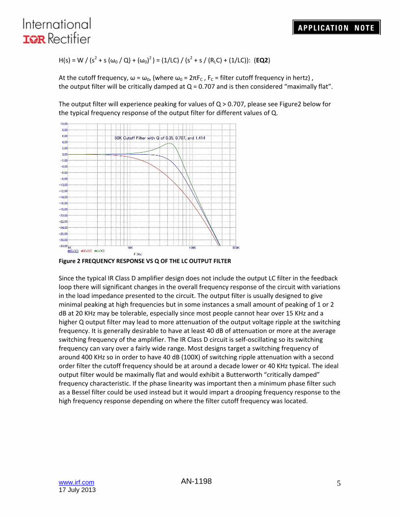
2 ) = (1/LC) / (s2 + s / (RLC) + (1/LC)): (EQ2) At the cutoff frequency, ω = ω0, (where ω0 = 2πFC , FC = filter cutoff frequency in hertz) , the output filter will be critically damped at Q = 0.707 and is then considered “maximally flat”. The output filter will experience peaking for values of Q > 0.707, please see Figure2 below for the typical frequency response of the output filter for different values of Q.
Figure 2 FREQUENCY RESPONSE VS Q OF THE LC OUTPUT FILTER
Since the typical IR Class D amplifier design does not include the output LC filter in the feedback loop there will significant changes in the overall frequency response of the circuit with variations in the load impedance presented to the circuit. The output filter is usually designed to give minimal peaking at high frequencies but in some instances a small amount of peaking of 1 or 2 dB at 20 KHz may be tolerable, especially since most people cannot hear over 15 KHz and a higher Q output filter may lead to more attenuation of the output voltage ripple at the switching frequency. It is generally desirable to have at least 40 dB of attenuation or more at the average switching frequency of the amplifier. The IR Class D circuit is self‐oscillating so its switching frequency can vary over a fairly wide range. Most designs target a switching frequency of around 400 KHz so in order to have 40 dB (100X) of switching ripple attenuation with a second order filter the cutoff frequency should be at around a decade lower or 40 KHz typical. The ideal output filter would be maximally flat and would exhibit a Butterworth “critically damped” frequency characteristic. If the phase linearity was important then a minimum phase filter such as a Bessel filter could be used instead but it would impart a drooping frequency response to the high frequency response depending on where the filter cutoff frequency was located.
www.irf.com 17 July 2013
6AN-1198
5. Output Inductor Choice: The choice of output inductors is critical and affects both the overall total harmonic distortion of the amplifier and its efficiency. As stated before the output filter is not included in the feedback loop so any kind of non‐ linearity in the inductance will directly influence the performance of the amplifier. Also its core loss is critical to the efficiency of the design as even at idle in a Class AD design there will be a 50% duty cycle square wave across it with high voltage and high frequency. If the core material is not chosen carefully there will be a substantial amount of heat dissipated in the output inductors and this will lead to high operating temperatures in this filter component and high idle power losses. In some instances where this choice was not made wisely these parts may actually get hot to the touch. In many instances the best core material to use is gapped ferrite as it possesses low core loss and excellent linearity.
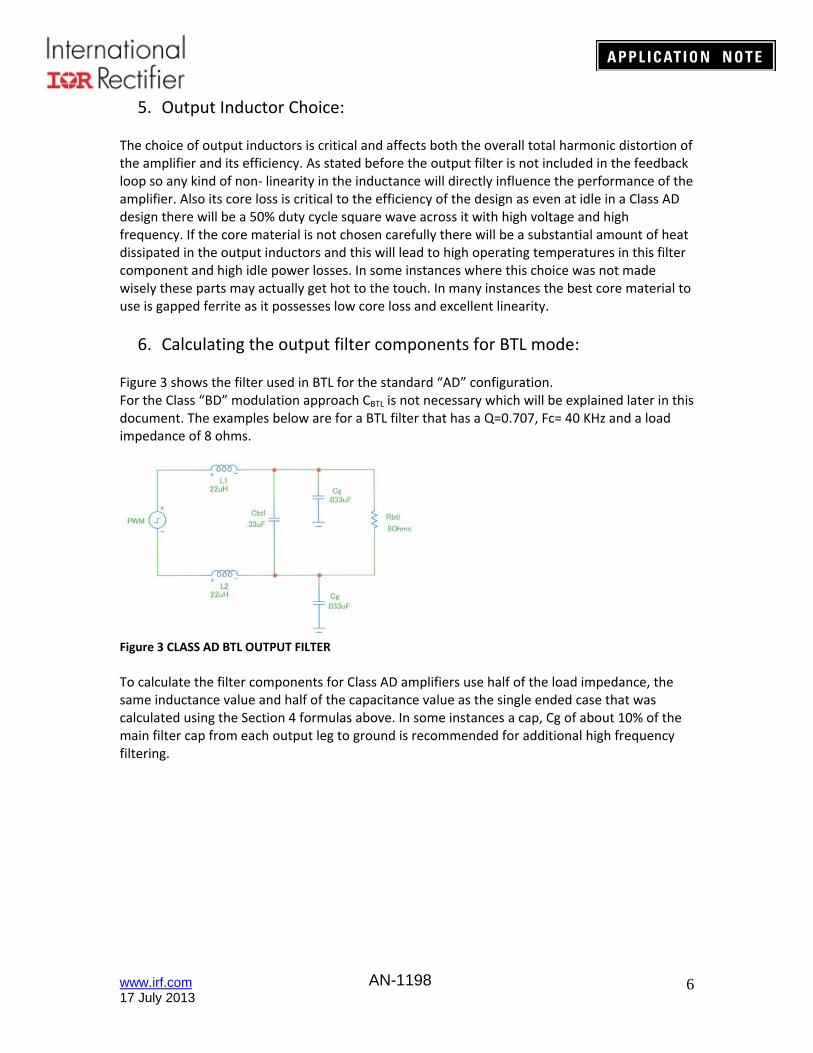
6. Calculating the output filter components for BTL mode: Figure 3 shows the filter used in BTL for the standard “AD” configuration. For the Class “BD” modulation approach CBTL is not necessary which will be explained later in this document. The examples below are for a BTL filter that has a Q=0.707, Fc= 40 KHz and a load impedance of 8 ohms.
Figure 3 CLASS AD BTL OUTPUT FILTER
To calculate the filter components for Class AD amplifiers use half of the load impedance, the same inductance value and half of the capacitance value as the single ended case that was calculated using the Section 4 formulas above. In some instances a cap, Cg of about 10% of the main filter cap from each output leg to ground is recommended for additional high frequency filtering.

www.irf.com 17 July 2013
7AN-1198
Figure 4 CLASS AD BTL FILTER EQUIVALENT CKT
In Figure 3 above Class AD filter, add 2X Cg capacitors differentially connected to ground to provide extra high frequency filtering; make the value about 10% of the value of CBTL. The two capacitors are in series so substitute one capacitor of half the value instead across the load. If you are designing a Class BD amplifier then the equivalent circuit to use is below:
Figure 5 CLASS BD BTL FILTER EQUIVALENT CKT
Note that CBTL is absent for this modulation scheme, only differential filtering is required as there is no common mode output signal in this case. Use the same formulas as Section 4 above using half of the load impedance. For example do the calculations with a 4 ohm load if you are planning on BTL operation with an 8 ohm load.
7. Adding anti‐parallel diodes across the output to prevent false tripping of the overcurrent protection in the amplifier:
The overcurrent protection in IR Class D solutions can be activated if the load connected to the amplifier does not terminate the LC output filter properly or is grossly mismatched to its target design impedance. This happens when there is substantial noise or a large signal present on the output of the amplifier at the resonant frequency of the output filter. If there is insufficient resistive damping in the load this condition can excite a high Q resonant current in the output of the amplifier which the protection circuitry will interpret as an output fault, putting the amplifier into hiccup mode. Adding a pair of protection diodes to each of the two active outputs will eliminate this condition and shunt the resonant energy to the rails of the amplifier, permitting normal operation. The diodes would connect from each output node to the positive rail with the anode connected to the output node and the cathode connected to Vcc+. On the negative side the cathode(s) would connect to the output node and the anodes would be
www.irf.com 17 July 2013
8AN-1198
connected to the negative rail or ground depending on whether a unipolar or bipolar supply is employed. As an added bonus, these extra diodes will enhance the reliability of the amplifier in the event that current limiting is engaged due to this issue and eliminate potentially very high circulating current through the output devices. Either conventional silicon or Schottky diodes could possibly be used here. Schottky diodes may provide a bit more protection and will turn off more quickly once this condition is not present. This technique is effective in both half bridge and fully bridged applications where there is a high Q low DCR output filter.
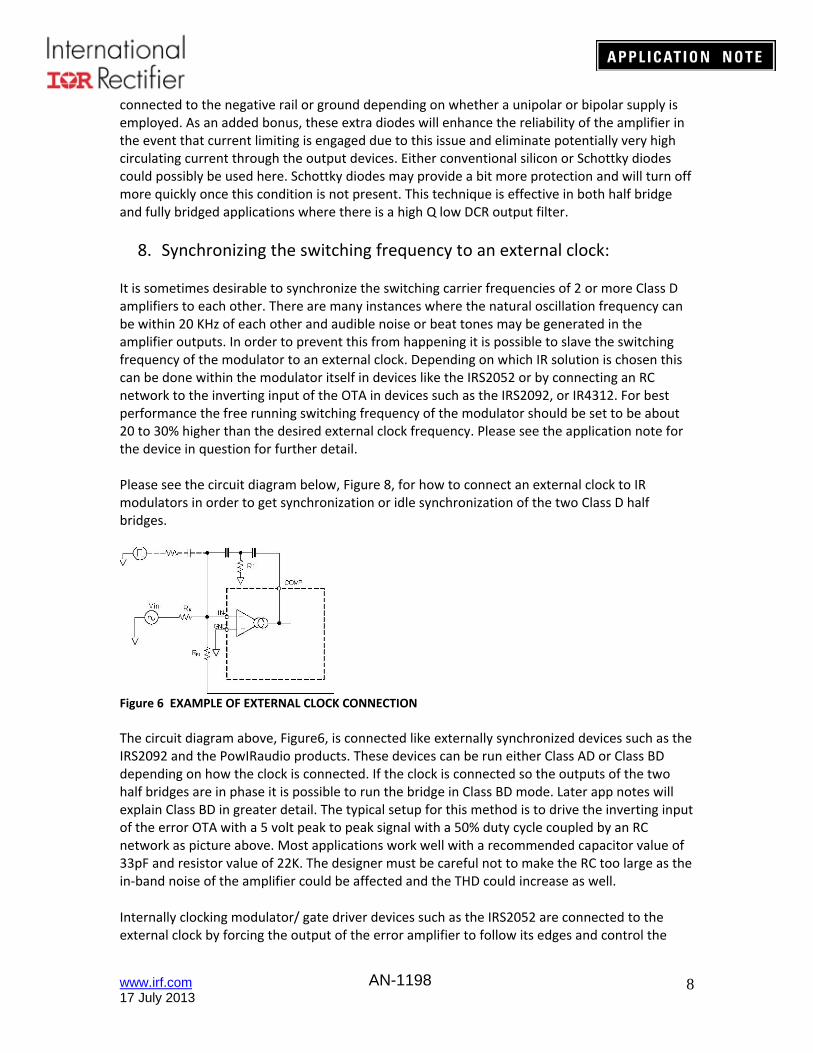
8. Synchronizing the switching frequency to an external clock: It is sometimes desirable to synchronize the switching carrier frequencies of 2 or more Class D amplifiers to each other. There are many instances where the natural oscillation frequency can be within 20 KHz of each other and audible noise or beat tones may be generated in the amplifier outputs. In order to prevent this from happening it is possible to slave the switching frequency of the modulator to an external clock. Depending on which IR solution is chosen this can be done within the modulator itself in devices like the IRS2052 or by connecting an RC network to the inverting input of the OTA in devices such as the IRS2092, or IR4312. For best performance the free running switching frequency of the modulator should be set to be about 20 to 30% higher than the desired external clock frequency. Please see the application note for the device in question for further detail. Please see the circuit diagram below, Figure 8, for how to connect an external clock to IR modulators in order to get synchronization or idle synchronization of the two Class D half bridges.
Figure 6 EXAMPLE OF EXTERNAL CLOCK CONNECTION
The circuit diagram above, Figure6, is connected like externally synchronized devices such as the IRS2092 and the PowIRaudio products. These devices can be run either Class AD or Class BD depending on how the clock is connected. If the clock is connected so the outputs of the two half bridges are in phase it is possible to run the bridge in Class BD mode. Later app notes will explain Class BD in greater detail. The typical setup for this method is to drive the inverting input of the error OTA with a 5 volt peak to peak signal with a 50% duty cycle coupled by an RC network as picture above. Most applications work well with a recommended capacitor value of 33pF and resistor value of 22K. The designer must be careful not to make the RC too large as the in‐band noise of the amplifier could be affected and the THD could increase as well.
Internally clocking modulator/ gate driver devices such as the IRS2052 are connected to the external clock by forcing the output of the error amplifier to follow its edges and control the
www.irf.com 17 July 2013
9AN-1198
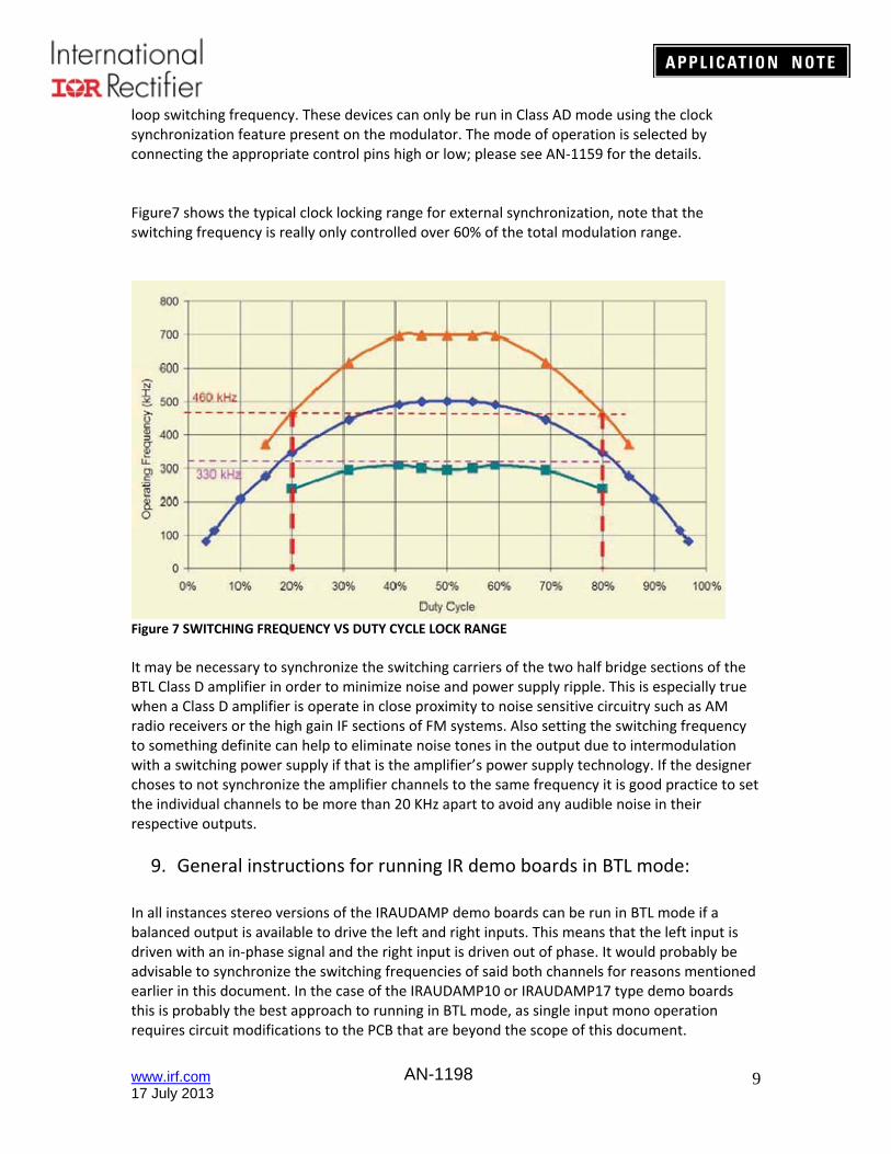
loop switching frequency. These devices can only be run in Class AD mode using the clock synchronization feature present on the modulator. The mode of operation is selected by connecting the appropriate control pins high or low; please see AN‐1159 for the details. Figure7 shows the typical clock locking range for external synchronization, note that the switching frequency is really only controlled over 60% of the total modulation range.
Figure 7 SWITCHING FREQUENCY VS DUTY CYCLE LOCK RANGE It may be necessary to synchronize the switching carriers of the two half bridge sections of the BTL Class D amplifier in order to minimize noise and power supply ripple. This is especially true when a Class D amplifier is operate in close proximity to noise sensitive circuitry such as AM radio receivers or the high gain IF sections of FM systems. Also setting the switching frequency to something definite can help to eliminate noise tones in the output due to intermodulation with a switching power supply if that is the amplifier’s power supply technology. If the designer choses to not synchronize the amplifier channels to the same frequency it is good practice to set the individual channels to be more than 20 KHz apart to avoid any audible noise in their respective outputs.
9. General instructions for running IR demo boards in BTL mode:
In all instances stereo versions of the IRAUDAMP demo boards can be run in BTL mode if a balanced output is available to drive the left and right inputs. This means that the left input is driven with an in‐phase signal and the right input is driven out of phase. It would probably be advisable to synchronize the switching frequencies of said both channels for reasons mentioned earlier in this document. In the case of the IRAUDAMP10 or IRAUDAMP17 type demo boards this is probably the best approach to running in BTL mode, as single input mono operation requires circuit modifications to the PCB that are beyond the scope of this document.
www.irf.com 17 July 2013
10AN-1198
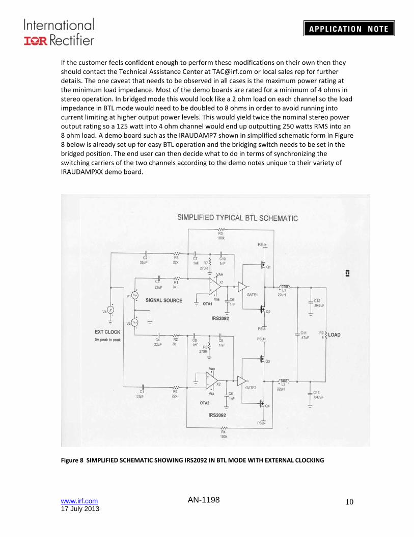
If the customer feels confident enough to perform these modifications on their own then they should contact the Technical Assistance Center at [email protected] or local sales rep for further details. The one caveat that needs to be observed in all cases is the maximum power rating at the minimum load impedance. Most of the demo boards are rated for a minimum of 4 ohms in stereo operation. In bridged mode this would look like a 2 ohm load on each channel so the load impedance in BTL mode would need to be doubled to 8 ohms in order to avoid running into current limiting at higher output power levels. This would yield twice the nominal stereo power output rating so a 125 watt into 4 ohm channel would end up outputting 250 watts RMS into an 8 ohm load. A demo board such as the IRAUDAMP7 shown in simplified schematic form in Figure 8 below is already set up for easy BTL operation and the bridging switch needs to be set in the bridged position. The end user can then decide what to do in terms of synchronizing the switching carriers of the two channels according to the demo notes unique to their variety of IRAUDAMPXX demo board.
Figure 8 SIMPLIFIED SCHEMATIC SHOWING IRS2092 IN BTL MODE WITH EXTERNAL CLOCKING

www.irf.com 17 July 2013
11AN-1198
10. Nominal bridged power output levels for the PowIRaudio line of products.
The PowIRaudio line of product is naturally configured for bridged Class D operation as the inputs are fully differential and the input signal can be referred to ground with no loss of performance or fidelity. Below is a chart that indicates the maximum power output of the IR4302, IR4312, and IR4322 at various load impedances:
Figure 9. A 7 x 7 QFN 2ch half bridge Class D Amplifier (IR43X2)
Part Number Load
Impedance No
Heatsink 8 C/W Heatsink
Max PSU Voltage under loaded cond’s
IR4302 8 OHMS 140W 260W 62V
6 OHMS 100W 200W
4 OHMS 80W 140W
IR4322 8OHMS 170W 200W 50V
6 OHMS 140W 250W
4 OHMS 100W 200W
IR4312 8 OHMS 60W N/A 32V
6 OHMS 80W
4 OHMS 90W NOTE: For Heatsink recommendations please see PowIRaudio app notes.
Please see their respective datasheets for thermal and electrical limits.

www.irf.com 17 July 2013
12AN-1198
Figure 10. Typical schematic of a PowIRaudio 2 channel Class D amplifier during bridged operation. Summary: Many Class D switching amplifier applications can benefit from BTL output operation. All of IR’s Class D product offerings can be configured to operate in bridged mode by observing the design rules that were expounded upon in this application note. Bridged mode allows for up to 4X the output power and twice the output voltage swing for the same output load impedance. The PowIRaudio product line makes it especially easy to operate in BTL mode due to their differential input structures which enables the input signal to be referenced to ground. They also allow for easy implementation of a unipolar power supply to feed the amplifier’s output stages which can save the designer considerable component cost. We invite you to please visit the irf.com website and explore our application notes library for further technical information.


![DUCATI 1198 / 1198 S (2009) - JAMparts · PDF file6`gVedk^X Y#Y# '%%. Vaa g^\]ih gZhZgkZY DUCATI 1198 / 1198 S (2009) EVOLUTION EXHAUST SYSTEM Product code: (109190) S-D10EFT3T-ZC,](https://img.pdfslide.us/doc/110x75/5a78c5757f8b9a21538d2018/ducati-1198-1198-s-2009-jamparts-gvedkx-yy-vaa-gih-gzhzgkzy-ducati.jpg)