Embed Size (px)
DESCRIPTION
Aplication Note for MBI6024
Citation preview

Confidential
____________________ MBI6024 Application Note V2.02- EN____________________
1
MBI6024 Application Note
Foreword The MBI6024 is a constant current LED driver for LED strips applications. The stability of data transmission
has been improved through clock reverse and A-TokenTM topology. This article mainly addresses five
chapters:
1. The strip design, LED and gray scale setting…etc.
2. The controller signal design, including notice for controller, CKI frequency notice… etc.
3. The production and setup, including the effect of hot swap, the design to reduce the surge voltage…etc.
4. The method of system testing.
5. Other applications notice, such as high VLED application.
Chapter 1. Strips Design Figure 1 shows the MBI6024 application circuit.
⋯ ⋯
Figure 1. MBI6024 application circuit
!"#$%&'(()&)*%'$)+,-!"#$%&'(()&)*)*'."/0123!4567
Confidential
____________________ MBI6024 Application Note V2.02- EN____________________
©Macroblock, Inc. 2012 Floor 6-4, No. 18, Pu-Ting Rd., Hsinchu, Taiwan 30077, ROC.
TEL: +886-3-579-0068, FAX: +886-3-579-0125 E-mail: [email protected]
2
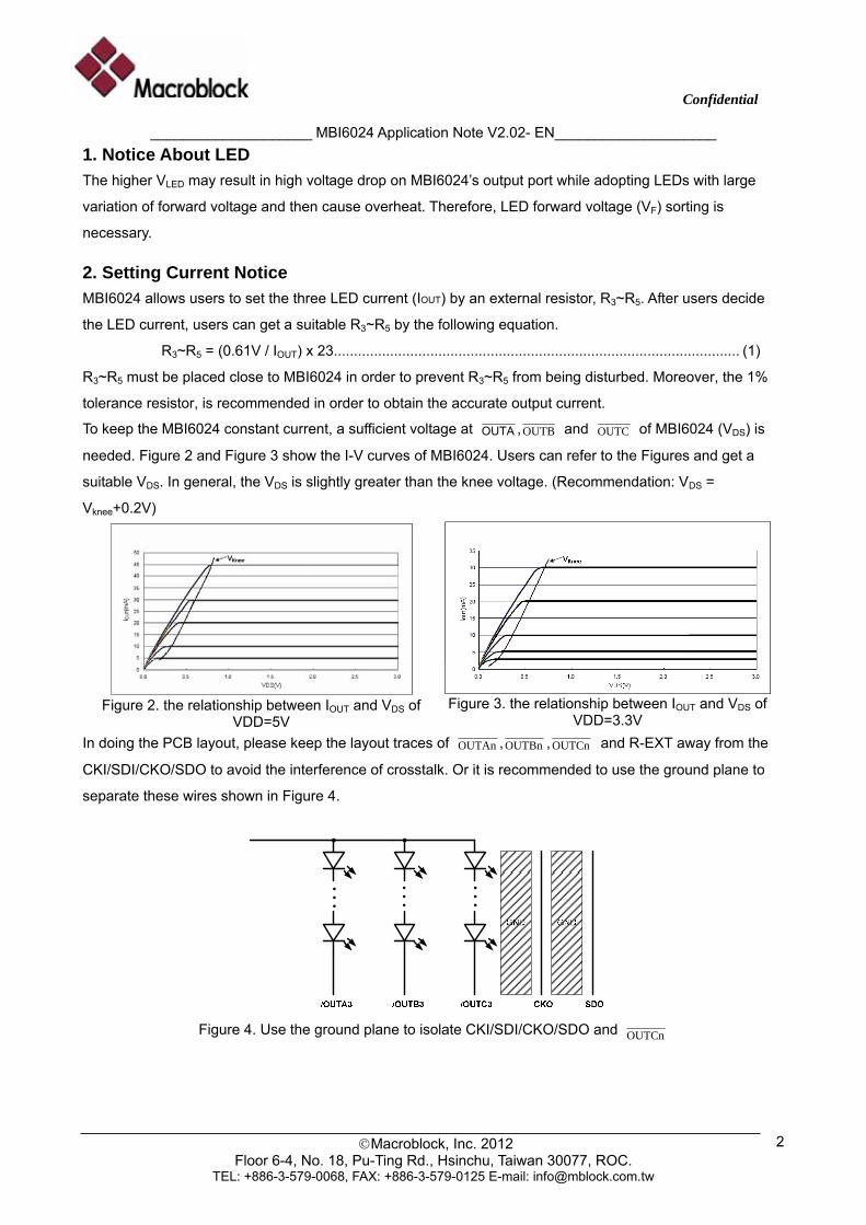
1. Notice About LED The higher VLED may result in high voltage drop on MBI6024’s output port while adopting LEDs with large
variation of forward voltage and then cause overheat. Therefore, LED forward voltage (VF) sorting is
necessary.
2. Setting Current Notice MBI6024 allows users to set the three LED current (IOUT) by an external resistor, R3~R5. After users decide
the LED current, users can get a suitable R3~R5 by the following equation.
R3~R5 = (0.61V / IOUT) x 23..................................................................................................... (1)
R3~R5 must be placed close to MBI6024 in order to prevent R3~R5 from being disturbed. Moreover, the 1%
tolerance resistor, is recommended in order to obtain the accurate output current.
To keep the MBI6024 constant current, a sufficient voltage at OUTA ,OUTB and OUTC of MBI6024 (VDS) is
needed. Figure 2 and Figure 3 show the I-V curves of MBI6024. Users can refer to the Figures and get a
suitable VDS. In general, the VDS is slightly greater than the knee voltage. (Recommendation: VDS =
Vknee+0.2V)
Figure 2. the relationship between IOUT and VDS of
VDD=5V Figure 3. the relationship between IOUT and VDS of
VDD=3.3V In doing the PCB layout, please keep the layout traces of OUTAn ,OUTBn ,OUTCn and R-EXT away from the
CKI/SDI/CKO/SDO to avoid the interference of crosstalk. Or it is recommended to use the ground plane to
separate these wires shown in Figure 4.
. . .
. . .
. . .
Figure 4. Use the ground plane to isolate CKI/SDI/CKO/SDO and OUTCn

Confidential
____________________ MBI6024 Application Note V2.02- EN____________________
©Macroblock, Inc. 2012 Floor 6-4, No. 18, Pu-Ting Rd., Hsinchu, Taiwan 30077, ROC.
TEL: +886-3-579-0068, FAX: +886-3-579-0125 E-mail: [email protected]
3
3. Setting LED Power The minimum VLED can be determined by the following equation
VLED, MIN. = (VF, MAX. x n) + VDS ................................................................................................. (2)
VDS
VLED
n
VF
+
-
GND
VDD OUTA0 OUTC3
CKI
SDI
R-EXTA R-EXTB R-EXTC
CKO
SDOMBI6024GP
1
2
3
9 10 11
12 24 13
7
6
⋯⋯⋯⋯
GND8
Figure 5. The sketch of minimum VLED voltage
where VF,MAX represents the maximum forward voltage of LED, and n is the number of cascaded LEDs. The
maximum sustaining voltage of /OUTn is 17V. If the supply voltage of LED (VLED) is over 17V, the IC will be
damaged. For the higher VLED application, please refer the P.16.
4. Power Configuration Because of the impedance of power lines, the voltage of each cluster might be different in the multi-cluster
cascaded application as shown in Figure 6. Users have to calculate the dropout voltage caused by the
impedance of power line. For example, the maximum conductor impedance of AWG26 (Maximum Conductor
Resistance) of UL1007 is 152Ω/km. It means that 1km transmission line is equal to 150Ω. If transmission line
is 50cm and current is 20mA, there will be 1.52mV voltage drop. If the voltage is lower than that of DC/DC
converter supply voltage, users should use a new power line, as shown in Figure 9 and Figure 10.
Figure 6. The sketch of dropout voltage in multi-cluster cascaded application

Confidential
____________________ MBI6024 Application Note V2.02- EN____________________
©Macroblock, Inc. 2012 Floor 6-4, No. 18, Pu-Ting Rd., Hsinchu, Taiwan 30077, ROC.
TEL: +886-3-579-0068, FAX: +886-3-579-0125 E-mail: [email protected]
4
Figure 7. The poor waveform of power
Figure 8. The poor waveform of power
DC/DC Converter
GND
VDD OUTA0 OUTC3
CKI
SDI
R-EXTA R-EXTB R-EXTC
CKO
SDOMBI6024GP
C20.1uF
1
2
3
9 10 11
12 24 13
7
6
C110uFTVS2
GND
VLED
LDO
J1 ⋯⋯VIN
GNDJ3VIN
GND8
Figure 9. The proposed method of the power
Figure 10. The power distribution of clusters
IC power IC power
Confidential
____________________ MBI6024 Application Note V2.02- EN____________________
©Macroblock, Inc. 2012 Floor 6-4, No. 18, Pu-Ting Rd., Hsinchu, Taiwan 30077, ROC.
TEL: +886-3-579-0068, FAX: +886-3-579-0125 E-mail: [email protected]
5
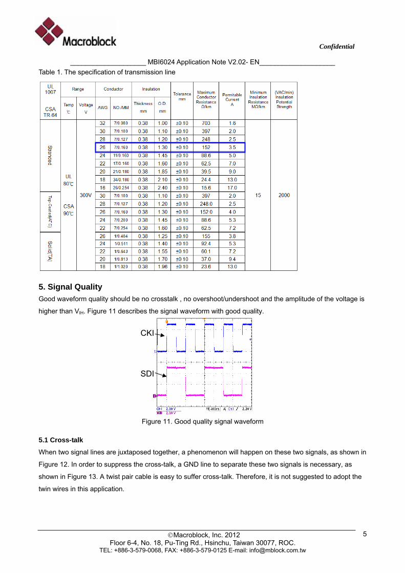
Table 1. The specification of transmission line
5. Signal Quality Good waveform quality should be no crosstalk , no overshoot/undershoot and the amplitude of the voltage is
higher than VIH. Figure 11 describes the signal waveform with good quality.
Figure 11. Good quality signal waveform
5.1 Cross-talk
When two signal lines are juxtaposed together, a phenomenon will happen on these two signals, as shown in
Figure 12. In order to suppress the cross-talk, a GND line to separate these two signals is necessary, as
shown in Figure 13. A twist pair cable is easy to suffer cross-talk. Therefore, it is not suggested to adopt the
twin wires in this application.
CKI
SDI

Confidential
____________________ MBI6024 Application Note V2.02- EN____________________
©Macroblock, Inc. 2012 Floor 6-4, No. 18, Pu-Ting Rd., Hsinchu, Taiwan 30077, ROC.
TEL: +886-3-579-0068, FAX: +886-3-579-0125 E-mail: [email protected]
6
Figure 12. The waveform of cross-talk
Figure 13. The arrangement of transmission line
In order to reduce the noise interference, the cable wire with shield is recommended to be the transmission
line; also, the braid and drain wire of foil must connect to ground.
Figure 14. The cable wire with shield
CKI
SDI

Confidential
____________________ MBI6024 Application Note V2.02- EN____________________
©Macroblock, Inc. 2012 Floor 6-4, No. 18, Pu-Ting Rd., Hsinchu, Taiwan 30077, ROC.
TEL: +886-3-579-0068, FAX: +886-3-579-0125 E-mail: [email protected]
7
5.2 Overshoot / Undershoot Voltage Figure 15 shows the overshoot and undershoot voltage on CKI and SDI signals. In order to improve the
signal quality, it is recommend to reserve the PCB positions of R1 and R2 in Figure 16 The resistance of R1
and R2 will affect the rising and falling time of CKO/SKO. The larger resistance results in slower rising/falling
time and reduce the effect of over/undershoot voltage. However, the large resistance might cause abnormal
transmission.
Figure 15. The poor waveform of overshoot or undershoot voltage
Figure 16. The sketch of how to improve the poor waveform
5.3 Amplitude The factors that affect amplitude include equivalent capacitance of wire, equivalent capacitance of TVS,
voltage of VDD and resistance of CKO/SDO. User can choose shorter wire to reduce the equivalent
capacitance and smaller equivalent capacitance of TVS and adjust resistance of CKO/SDO.
Figure 17. The poor waveform of insufficient amplitude
6. Notice About Test Pin
The pin 4 and pin 5 of GP package and pin 13 and pin14 of GFN package are test pins. Please not connect
these pins to avoid IC into test mode.
CKI
SDI
CKI
SDI

Confidential
____________________ MBI6024 Application Note V2.02- EN____________________
©Macroblock, Inc. 2012 Floor 6-4, No. 18, Pu-Ting Rd., Hsinchu, Taiwan 30077, ROC.
TEL: +886-3-579-0068, FAX: +886-3-579-0125 E-mail: [email protected]
8
Chapter 2. Control Signal Design
1. Notice for Controller
To improve the validity of control signal, the control signal should be output after the power supplies of
controller and module are stable and use the circuit of power on reset to initialize MBI6024. The transmission
lines of CKI and SDI from controller to first cluster should be separated by a ground line and add a GND on
connector to be the common ground.
2. CKI frequency Notice
The minimum CKI frequency of MBI6024 is 200kHz. Users should use fixed CKI frequency to improve
system stability.
3. CKI Stop Time
The time-out protection of MBI6024 is to check the validity of data counter by counting the duration of CKI
stop through the internal counter. When the CKI stop time in one frame exceeds 95-CKI, MBI6024 will ignore
the present input data and keep the previous data until the correct data is inputted.
Figure 18. Diagram of CKI stop time
4. Command Notice
The configuration and dot correction data should be re-sent pre-fixed time by controller. Users can re-send
the configuration data (CF1[7] must be 1) pre-fixed time only, if the dot correction function is unnecessary. .
The dot correction data is executed by inputting new gray scale data, it should be inputted first, and then
input the gray scale data.
5. Input Signal
The output signal of controller should allow the falling edge of CKI in the middle of SDI data. The
recommended CKI is 50% of the duty, as shown in Figure 19.
Figure 19. The falling edge of CKI in the middle of SDI data
The correct input signal format should consist of Prefix, Header and Data.
Confidential
____________________ MBI6024 Application Note V2.02- EN____________________
©Macroblock, Inc. 2012 Floor 6-4, No. 18, Pu-Ting Rd., Hsinchu, Taiwan 30077, ROC.
TEL: +886-3-579-0068, FAX: +886-3-579-0125 E-mail: [email protected]
9
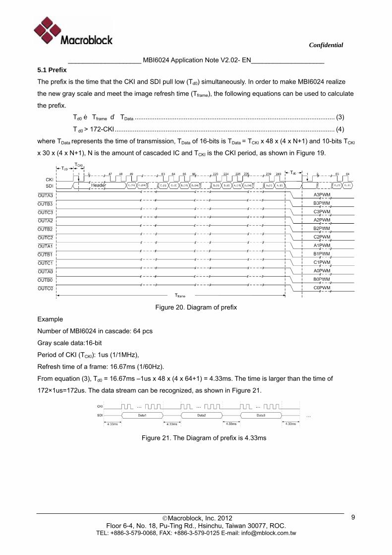
5.1 Prefix
The prefix is the time that the CKI and SDI pull low (Td0) simultaneously. In order to make MBI6024 realize
the new gray scale and meet the image refresh time (Tframe), the following equations can be used to calculate
the prefix.
Td0 ≦ Tframe - TData .............................................................................................................. (3)
T d0 > 172-CKI ......................................................................................................................... (4)
where TData represents the time of transmission, TData of 16-bits is TData = TCKI x 48 x (4 x N+1) and 10-bits TCKI
x 30 x (4 x N+1), N is the amount of cascaded IC and TCKI is the CKI period, as shown in Figure 19.
Figure 20. Diagram of prefix
Example
Number of MBI6024 in cascade: 64 pcs
Gray scale data:16-bit
Period of CKI (TCKI): 1us (1/1MHz),
Refresh time of a frame: 16.67ms (1/60Hz).
From equation (3), Td0 = 16.67ms –1us x 48 x (4 x 64+1) = 4.33ms. The time is larger than the time of
172×1us=172us. The data stream can be recognized, as shown in Figure 21.
Figure 21. The Diagram of prefix is 4.33ms

Confidential
____________________ MBI6024 Application Note V2.02- EN____________________
©Macroblock, Inc. 2012 Floor 6-4, No. 18, Pu-Ting Rd., Hsinchu, Taiwan 30077, ROC.
TEL: +886-3-579-0068, FAX: +886-3-579-0125 E-mail: [email protected]
10
5.2 Header
The correct Header must be transmitted before the gray scale data to make sure each MBI6024 can catch
the gray scale data with correct address. The header includes H(Command Header), A(Address), L(Length)
and P(Parity Check).
5.2.1 Command Header illustration
MBI6024 has six types of Command Headers, as shown in Table 2. According to the definition of each
header, the consequent data will be written to gray scale data, dot correction data, configure data.
Table 2. Six kinds of command
5.2.2 Address and Length Illustration
A-TokenTM is the address setting method of MBI6024. The theorem of A-TokenTM is to distribute the
A(Address) and L(Length) to each IC automatically. The address data will add 1 whenever the data chain
pass to the next IC, and the Least Significant Bit (LSB) will be exported first to address the next IC. When the
data of A(Address) and L(length) are the same, the data will be latched to register. The L(length) of
MBI6024 is the amount of cascaded ICs minus one. For example, if there are three MBI6024 in cascaded,
the L(Length) will be 2(10’b0000000010), and the initial A(Address) is 0(10b’0000000000).
Figure 22. Diagram of A-TokenTM
5.2.3 Parity Check Illustration
The parity check function is to check if there is any error data on the Command Header, Address and Length.
When parity check is enabled, if the count of parity is incorrect shows on the Command Header, Address or
Length, the data chain will be invalid and the IC keeps the previous frame data until the result of parity check
is correct. The default value of parity check is disabled, users can set CF1[0]= “1” to enable the parity check
function. The example of parity check shows below. The P[3] of parity check is the odd/even result of P[2:0],
as shown in Figure 23.
Figure 23. The example of parity check

Confidential
____________________ MBI6024 Application Note V2.02- EN____________________
©Macroblock, Inc. 2012 Floor 6-4, No. 18, Pu-Ting Rd., Hsinchu, Taiwan 30077, ROC.
TEL: +886-3-579-0068, FAX: +886-3-579-0125 E-mail: [email protected]
11
Following shows the example of two MBI6024 in cascade with different commands.
16- bit Configuration Data
Figure 24. The example of 16-bit configuration data
where the configuration data of each IC only needs 3 x 16 bits. As the Length data sets 1(10’b0000000001),
the length of configuration data is 2 x 3 x 16 bits. X2 and CF1 will be sent twice continuously, and following
by X3 and CF2. Each bit defines as below.
CF1:
Bit Function 9:8 GCLK frequency = 10 (internal oscillator divided by two) 7 Dot correction mode =0(enable dot correction)
6:5 11 4 PWM counter reset = 1(PWM counter reset after configuring control register) 3 PWM data synchronization =1(Automatic synchronization)
2:1 Phase-inversed output clock = 11 0 Parity check =1(Enable)
CF2:
Bit Function 2:0 111
10- bit Configuration Data
Figure 25. The example of 10-bit configuration data
where configuration data of each IC only needs 3 x 10 bits. As the Length data sets 1(10’b0000000001), it
totally needs 2 x 3 x 10 bits of configuration data after the Header. The data string of CF1 should be inputted
twice, then CF2, The definition of each bit is the same as 16-bit configuration data.

Confidential
____________________ MBI6024 Application Note V2.02- EN____________________
©Macroblock, Inc. 2012 Floor 6-4, No. 18, Pu-Ting Rd., Hsinchu, Taiwan 30077, ROC.
TEL: +886-3-579-0068, FAX: +886-3-579-0125 E-mail: [email protected]
12
8- bit Dot Correction Data
Figure 26. The example of 8-bit dot correction data
where two Command Headers must be filled with 6b’110011 in the Header. Every 8-bit dot correction data
must be filled twice continuously. As the Length sets 1(10’b0000000001), it totally needs 2 x 3 x 4 x 16 bits of
dot correction data after the Header.
6- bit Dot Correction Data
Figure 27. The example of 6-bit dot correction data
where two Command Headers must be filled with 6b’10011 in the Header. As the Length sets
1(10’b0000000001), it totally needs 2 x 3 x 4 x 10 bits of dot correction data after the Header.
16- bit Gray Scale Data
Figure 28. The example of 16-bit gray scale data
where two Command Header must be filled with 6b’111111 in the Header. As the Length sets
1(10’b0000000001), it needs 2 x 3 x 4 x 16 bits gray scale data after the Header.
10- bit Gray Scale Data
Figure 29. The example of 10-bit gray scale data
where two Command Header must be filled with 6b’101011 in the Header. As the Length sets
1(10’b0000000001), it needs 2 x 3 x 4 x 10 bits gray scale data after the Header.

Confidential
____________________ MBI6024 Application Note V2.02- EN____________________
©Macroblock, Inc. 2012 Floor 6-4, No. 18, Pu-Ting Rd., Hsinchu, Taiwan 30077, ROC.
TEL: +886-3-579-0068, FAX: +886-3-579-0125 E-mail: [email protected]
13
Chapter 3. Production and Setup
1. The Effect of Hot Swap Hot swapping means the action of connecting or disconnecting the pin of VDD/CKI/SDI/CKO/SDO of
MBI6024. It will induce the heavy instantaneous current and high voltage, and then damage the IC. Besides
increasing the EOS protection component as mentioned, users also may add the longer ground terminal in
connectors, and operate the correct procedures to avoid hot swap.
2. Design to Reduce Strike Voltage
2.1 Resistance
Cascade a resistor at CKO and SDO can reduce the probability of IC been damaged by hot swap. The larger
resistance results the lower probability of damage problem, and the lower speed of transmission. The
recommended resistances of R2 and R3, which are shown in Figure 16, are 33Ω.
2.2 Connector
When setting up or removing the connecter of cluster instantly, in order to reduce the unexpected spike
voltage and to avoid IC been burned out, users need to turn off the power, and then set up or remove the
cluster. It is better to connect GND first. Users can design the longer GND terminal in connector pin than in
VDD terminal in connector to reduce the unexpected strike voltage, as shown in Figure 30.
Figure 30. The safety design of longer terminal ground
2.3 Transient Voltage Suppressor
All Macroblock products have passed the standard of ESD protection. But to enhance the capacity of
Electrical Over Stress (EOS) protection, an external device, Transient Voltage Suppressor (TVS), is
necessary. Figure 31 shows the positions of TVS1~TVS4, and followings are the guidelines for TVS selection.
Select TVS1
a. The maximum Reverse Stand-Off Voltage (VRWM) should be equal to module’s input voltage.
b. The maximum clamping voltage (VC) should be 1V~2V higher than module’s input voltage.
c. The maximum Peak Pulsed Power (PPPM) is the product of maximum clamping voltage and peak pulse
current.
d. TVS diode should be placed to the pins that need to protect as close as possible to prevent the EOS.
Select TVS2
a. The maximum Reverse Stand-Off Voltage (VRWM) should be equal to 5V.
b. The maximum clamping voltage (VC) should be equal to 7V.
c. The maximum Peak Pulsed Power (PPPM) is the product of maximum clamping voltage and peak pulse
current.
d. TVS diode should be placed to the pins that need to protect as close as possible to prevent the EOS.

Confidential
____________________ MBI6024 Application Note V2.02- EN____________________
©Macroblock, Inc. 2012 Floor 6-4, No. 18, Pu-Ting Rd., Hsinchu, Taiwan 30077, ROC.
TEL: +886-3-579-0068, FAX: +886-3-579-0125 E-mail: [email protected]
14
Select TVS3 and TVS4
a. The maximum Reverse Stand-Off Voltage (VRWM) should be equal to 5V.
b. The maximum clamping voltage (VC) should be equal to 7V.
c. The maximum Peak Pulsed Power (PPPM) is the product of maximum clamping voltage and peak pulse
current.
d. TVS diode should be placed to the protected pins as close as possible to prevent the EOS happened.
e. For the high frequency loop, such as CKI/SDI/CKO/SDO, the parasitic capacitance of TVS will cause
noise and signal attenuation. The TVS with low parasitical capacitance is adapted in high frequency
application.
DC/DC Converter
GND
VDD OUTA0 OUTC3
CKI
SDI
R-EXTA R-EXTB R-EXTC
CKO
SDOMBI6024GP
C20.1uF
1
2
3
9 10 11
12 24 13
7
6CKISDI
C110uFTVS2
TVS3 TVS4
GNDCKOSDOGND
GND
R2
R1
VLED
LDO
J1 ⋯⋯VIN
connetc to VDD connetc to VDD
GNDJ3VIN
TVS1
option
option
GND8
Figure 31. Apply the electrical overstress protection
Figure 32. Without use EOS component
Figure 33. With use EOS component
3. Production and Setup procedures The following procedures should be observed in producing and installing the modules. In order to avoid the
controller from providing a valid power to the IC and cause the EOS through the ESD protection circuit.
Modules in the production and installation should carefully follow the correct procedures:
Step 1: Before install the module, please turn all the power off.
Step 2: The procedure of electrostatic discharge should be taken before connecting the cluster.
Step 3: Make sure the grounding system has been properly grounded.
Step 4: Make sure all the conducting wires of power supply and controller have completed and correctly
contacted with connector.
Step 5: After the above procedures have been executed, then start the system power supply.
Step 6: After the system power is stable, then start the controller power supply.

Confidential
____________________ MBI6024 Application Note V2.02- EN____________________
©Macroblock, Inc. 2012 Floor 6-4, No. 18, Pu-Ting Rd., Hsinchu, Taiwan 30077, ROC.
TEL: +886-3-579-0068, FAX: +886-3-579-0125 E-mail: [email protected]
15
Step 7: Before the procedures of cluster removing or repairing welding, users have to turn off the controller
power first and then the system power. After the residual charge has been completely discharged,
then the rework procedures can be executed.
Figure 34. Power-on sequence
4. Printed Circuit Board Notice 1. Users should avoid empty solder, cold solder, and split solder in manufacturing process of printed circuit
board (PCB).
2. Device layout should avoid approaching the board edge of PCB.
3. To design the longer size of PCB, it is suggested to select the thick slab value of PCB to avoid soldering
issues due to board bending.
Chapter 4. The Method of System Testing Please use the Configuration Data, Dot Correction Data and Gray Scale Data for system testing. The CKI
frequency is 1MHz, RGB gray scale data is 10’b0101010101, and the LED turns on sequence is
R G B R G…. If the LED works normally, the CKI frequency can be increased to 500kHz until LED
works abnormally. If the LED can’t work normally, then the CKI frequency should be decreased. The lowest
CKI frequency is 200kHz. If LED still can’t work under this frequency, please check if the signals of CKI and
SKI have been distorted.

Confidential
____________________ MBI6024 Application Note V2.02- EN____________________
©Macroblock, Inc. 2012 Floor 6-4, No. 18, Pu-Ting Rd., Hsinchu, Taiwan 30077, ROC.
TEL: +886-3-579-0068, FAX: +886-3-579-0125 E-mail: [email protected]
16
Chapter 5. Other application Notice
1. Higher VLED Application In more cascaded LEDs strings application, if the VLED is larger than the sustaining voltage of /OUTAn,
MBI6024 might be damaged when the IC is turned off. The simplest method is to parallel a resistor (R6 ~ R17)
at the output terminals of MBI6024, as shown in Figure 35. When the IC is turned off, the LED will generate a
small current from the paralleled resistor, and then the VDS will not exceed the sustaining voltage of output
terminal.
⋯ ⋯
Figure 35. The application circuit of high VLED
Users can follow the steps below to calculate the paralleled resistor.
1. Find out the LED current (ILED-CUT), which results in the invisible LED brightness.
2. Calculate the resistor
R6 ~ R17 = (VLED – N x VF, LED-CUT (MAX)) / ILED-CUT ..................................................................... (5)
where N is the cascaded LED number, and VF, LED-CUT (MAX) is the LED forward voltage under ILED-CUT.The
calculation of VLED – N x VF, LED-CUT (MAX) must be smaller that the sustaining voltage of MBI6024’s output
terminal.
3. Parallel the R6 ~ R17 to the output terminal and turn off MBI6024. Make sure the LED brightness is invisible
and VDS is smaller than 17V.

Confidential
____________________ MBI6024 Application Note V2.02- EN____________________
©Macroblock, Inc. 2012 Floor 6-4, No. 18, Pu-Ting Rd., Hsinchu, Taiwan 30077, ROC.
TEL: +886-3-579-0068, FAX: +886-3-579-0125 E-mail: [email protected]
17
Example: The VLED is 24V, and the cascaded LED number is 11. Please calculate the paralleled resistor to
prevent the IC from being damaged.
Table 3. The example of LED I-V data
1. Find out the ILED-CUT
Table 3 is the I-V data of the LED in this example, and the ILED-CUT on this table is 0.0024mA.
2. From equation (5), the R6 ~ R17 are (24V – 11 x 1.48V) / 0.0024mA = 3.2MΩ. In this example, select a
3.3MΩ resistor with 0603 package to be R6 ~ R17. And when IC turns off the VDS should be
24V – 11 x 1.48V = 7.72V. It is smaller than 17V.
When R6 ~ R17 are connected to the output terminals, and MBI6024 are turned off, the measured VDS is
7.61V, and the LED current is 0.0023mA. So that the LED brightness is invisible.
2. Logic Level Issue If users have to use the long power line on the PCB, the distributed capacitors, which Figure 36 shows, are
recommended. The value of Cd depends on the distance between each power line.
Figure 36. The sketch of distributed capacitance
3. Logic Level Issue Due to voltage drop effect, the VDD of each cluster is different. it will lead to different logic level between
clusters, as shown in Figure 37. When VDD is 5V, the VIH/VIL level will be 3.65V/1.4V respectively. And if the
VDD of another cluster is 4V, the logic level will be 2.92V/1.12V. The different logic level will cause a different
trigger time and then impact the signal transmission. Please refer to the section of "Power Configuration" for
the suggested method.
Figure 37. The diagram of different VDD

Confidential
____________________ MBI6024 Application Note V2.02- EN____________________
©Macroblock, Inc. 2012 Floor 6-4, No. 18, Pu-Ting Rd., Hsinchu, Taiwan 30077, ROC.
TEL: +886-3-579-0068, FAX: +886-3-579-0125 E-mail: [email protected]
18
Summary In the application of multiple clusters cascaded, the following notices must be taken
1. The transmission line with small parasitic inductance is required to enhance the signal quality.
2. To prevent the insufficient VLED, which is caused by the conductor resistance in transmission line, results
the problem of cluster brightness unbalance, please refer Figure 9 to design the power source.
3. Please refer to chapter 3, “Production and Installation”, to protect IC being damaged from hot-plug in.
Please take a note, even the processes in chapter 3 have been executed, it only can reduce the probability
of burn-out when hot-plug in, can’t totally solve the problem.