Embed Size (px)
Citation preview

Application Manual
Power Semiconductors
Application Manual
Power Semiconductors
Dr.-Ing. Arendt Wintrich Dr.-Ing. Ulrich Nicolai
Dr. techn. Werner Tursky Univ.-Prof. Dr.-Ing. Tobias Reimann
Published by
SEMIKRON International GmbH

Bibliographic information published by the Deutsche Nationalbibliothek
The Deutsche Nationalbibliothek lists this publication in the Deutsche Nationalbibliografi e;
detailed bibliographic data is available on the Internet under http://dnb.d-nb.de
The use of registered names, trade names, trademarks etc. in this publication does not imply, even
in the absence of a specifi c statement, that such names are exempt from the relevant protective laws
and regulations and therefore free for general use.
This manual has been developed and drawn up to the best of our knowledge. However, all information and data provided is considered non-binding and shall not create liability for us. Publication of this manual is done without consideration of other patents or printed publications and patent rights of any third party. All component data referred to in this manual is subject to further research and development and, therefore, is to be considered exemplary only. Binding specifi cations are provided exclusively in the actual product-related datasheets.
The publisher reserves the right not to be responsible for the accuracy, completeness or topicality of any direct or indirect references to or citations from laws, regulations or directives (e.g. DIN, VDI, VDE) in this publication. We recommend obtaining the respectively valid versions of the complete regulations or direc-tives for your own work.
ISBN 978-3-938843-66-6
ISLE Verlag 2011 © SEMIKRON International 2011 This manual is protected by copyright. All rights reserved including the right of reprinting, reproduc-tion, distribution, microfi lming, storage in data processing equipment and translation in whole or in part in any form.
Published by: ISLE Verlag, a commercial unit of the ISLE Association Werner-von-Siemens-Strasse 16, D-98693 Ilmenau, Germany
Printed by: W. Tümmels Buchdruckerei und Verlag GmbH und Co KG Gundelfi nger Strasse 20, D-90451 Nuremberg, Germany
Edited by: SEMIKRON International GmbH Sigmundstrasse 200, D-90431 Nuremberg, Germany
Printed in Germany

Preface
Since the fi rst Application Manual for IGBT and MOSFET power modules was published, these components have found their way into a whole host of new applications, mainly driven by the growing need for the effi cient use of fossil fuels, the reduction of environmental impact and the resultant increased use of regenerative sources of energy. General development trends (space requirements, costs, and energy effi ciency) and the advancement into new fi elds of application (e.g. decentralised applications under harsh conditions) bring about new, stricter requirements which devices featuring state-of-the-art power semiconductors have to live up to. For this reason, this manual looks more closely than its predecessor at aspects pertaining to power semiconductor application and also deals with rectifi er diodes and thyristors, which were last detailed in a SEMI-KRON manual over 30 years ago.
This manual is aimed primarily at users and is intended to consolidate experience which up till now has been contained in numerous separate articles and papers. For reasons of clarity and where deemed necessary, theoretical background is gone into briefl y in order to provide a better understanding of the subject matter. A deeper theoretical insight is provided in various highly-recommendable textbooks, some of which have been cited in the bibliography to this manual.
SEMIKRON's wealth of experience and expertise has gone into this advanced application manual which deals with power modules based on IGBT, MOSFET and adapted diodes, as well as recti-fi er diodes and thyristors in module or discrete component form from the point of view of the user. Taking the properties of these components as a basis, the manual provides tips on how to use and interpret data sheets, as well as application notes on areas such as cooling, power layout, driver technology, protection, parallel and series connection, and the use of transistor modules in soft switching applications.
This manual includes contributions from the 1998 "Application Manual for IGBT and MOSFET Power Modules" written by Prof. Dr.-Ing. Josef Lutz and Prof. Dr.-Ing. habil. Jürgen Petzoldt, whose authorship is not specifi cally cited in the text here. The same applies to excerpts taken from the SEMIKRON Power Semiconductor Manual by Dr.-Ing. Hans-Peter Hempel. We would like to thank everyone for granting their consent to use the relevant excerpts.
We would also like to take this opportunity to express our gratitude to Rainer Weiß and Dr. Uwe Scheuermann for their expertise and selfl ess help and support. Thanks also go to Dr.-Ing. Thomas Stockmeier, Peter Beckedahl and Thomas Grasshoff for proofi ng and editing the texts, and Elke Schöne and Gerlinde Stark for their editorial assistance.
We very much hope that the readers of this manual fi nd it useful and informative. Your feedback and criticism is always welcome. If this manual facilitates component selection and design-in tasks on your part, our expectations will have been met.
Nuremberg, Dresden, Ilmenau; November 2010
Arendt WintrichUlrich NicolaiTobias ReimannWerner Tursky

The eCommerce portal for power electronics is a holding company of the SEMIKRON group offer-ing worldwide, multi-lingual customer service with its expert hotline, online forum, TechChat or via email contact. Discover the service quality of SindoPower eCommerce. www.sindopower.com

I
Contents
1 Power Semiconductors: Basic Operating Principles ..................................................... 1
1.1 Basics for the operation of power semiconductors ...................................................... 11.2 Power electronic switches ............................................................................................ 5
2 Basics ............................................................................................................................... 13
2.1 Application fi elds and current performance limits for power semiconductors .............. 132.2 Line rectifi ers .............................................................................................................. 17
2.2.1 Rectifi er diodes .................................................................................................... 172.2.1.1 General terms ................................................................................................ 172.2.1.2 Structure and functional principle ................................................................... 182.2.1.3 Static behaviour ............................................................................................. 202.2.1.4 Dynamic behaviour ........................................................................................ 20
2.2.2 Thyristors ............................................................................................................. 222.2.2.1 General terms ................................................................................................ 222.2.2.2 Structure and functional principle ................................................................... 232.2.2.3 Static behaviour ............................................................................................. 252.2.2.4 Dynamic behaviour ........................................................................................ 26
2.3 Freewheeling and snubber diodes ............................................................................. 282.3.1 Structure and functional principle ........................................................................ 28
2.3.1.1 Schottky diodes ............................................................................................. 292.3.1.2 PIN diodes ..................................................................................................... 30
2.3.2 Static behaviour .................................................................................................. 322.3.2.1 On-state behaviour ........................................................................................ 322.3.2.2 Blocking behaviour ........................................................................................ 33
2.3.3 Dynamic behaviour .............................................................................................. 342.3.3.1 Turn-on behaviour ......................................................................................... 342.3.3.2 Turn-off behaviour .......................................................................................... 352.3.3.3 Dynamic ruggedness ..................................................................................... 43
2.4 Power MOSFET and IGBT ........................................................................................ 432.4.1 Structure and functional principle ........................................................................ 432.4.2 IGBT .................................................................................................................... 46
2.4.2.1 Static behaviour ............................................................................................. 482.4.2.2 Switching behaviour ....................................................................................... 492.4.2.3 IGBT – Concepts and new directions of development ................................... 54
2.4.3 Power MOSFET ................................................................................................... 612.4.3.1 Static behaviour ............................................................................................. 632.4.3.2 Switching behaviour ....................................................................................... 662.4.3.3 Latest versions and new directions of development ....................................... 69
2.5 Packaging .................................................................................................................. 722.5.1 Technologies ....................................................................................................... 73
2.5.1.1 Soldering ...................................................................................................... 732.5.1.2 Diffusion sintering (low-temperature joining technology) ................................ 732.5.1.3 Wire bonding ................................................................................................. 752.5.1.4 Pressure contact ............................................................................................ 752.5.1.5 Assembly and connection technology ............................................................ 762.5.1.6 Modules with or without base plate ............................................................... 78
2.5.2 Functions and features ........................................................................................ 802.5.2.1 Insulation ...................................................................................................... 802.5.2.2 Heat dissipation and thermal resistance ........................................................ 822.5.2.3 Power cycling capability ................................................................................. 912.5.2.4 Current conduction to the main terminals ...................................................... 912.5.2.5 Low-inductance internal structure .................................................................. 922.5.2.6 Coupling capacitances ................................................................................... 932.5.2.7 Circuit complexity........................................................................................... 94

II
2.5.2.8 Defi ned and safe failure behaviour in the event of module defects ................ 962.5.2.9 Environmentally compatible recycling ............................................................ 96
2.5.3 Discrete devices .................................................................................................. 972.5.3.1 Small rectifi ers ............................................................................................... 972.5.3.2 Stud-mounted diodes and stud thyristors ....................................................... 982.5.3.3 Disk cells ....................................................................................................... 982.5.3.4 SEMiSTART® ................................................................................................ 99
2.5.4 Power modules .................................................................................................. 1002.5.4.1 Basics .......................................................................................................... 1002.5.4.2 Module families containing diodes and thyristors ......................................... 1012.5.4.3 Module families including IGBT and freewheeling diodes ............................ 104
2.6 Integration of sensors, protective equipment and driver electronics .......................................................................................................110
2.6.1 Modules with integrated current measurement ...................................................1102.6.2 Modules with integrated temperature measurement ...........................................1112.6.3 IPM (Intelligent Power Module) ...........................................................................114
2.7 Reliability ...................................................................................................................1152.7.1 MTBF, MTTF and FIT rate ..................................................................................1162.7.2 Accelerated testing according to Arrhenius .........................................................1162.7.3 Standard tests for the product qualifi cation and postqualifi cation .......................117
2.7.3.1 High Temperature Reverse Bias Test (HTRB), High Temperature Gate Bias Test (HTGB), High Humidity High Temperature Reverse Bias Test (THB).....118
2.7.3.2 High and low temperature storage (HTS, LTS) .............................................1182.7.3.3 Temperature cycling test (TC) .......................................................................1182.7.3.4 Power cycling test (PC) ................................................................................1192.7.3.5 Vibration test ................................................................................................ 120
2.7.4 Additional tests for spring contacts ................................................................... 1202.7.4.1 Micro-vibration (fretting corrosion) .............................................................. 1202.7.4.2 Corrosive atmosphere (pollution gas test) .................................................. 1212.7.4.3 Contact-to-PCB temperature cycling ............................................................ 121
2.7.5 Failure mechanisms during power cycling ......................................................... 1222.7.6 Evaluation of temperature curves regarding module lifetime ............................. 126
3 Datasheet Ratings for MOSFET, IGBT, Diodes and Thyristors ................................... 131
3.1 Standards, symbols and terms ................................................................................. 1313.1.1 Standards .......................................................................................................... 1313.1.2 Letter symbols and terms .................................................................................. 1313.1.3 Maximum ratings and characteristics ................................................................ 1333.1.4 Component (type) designation system .............................................................. 133
3.2 Rectifi er diodes and thyristors .................................................................................. 1343.2.1 Temperatures..................................................................................................... 1343.2.2 Thermal impedance and thermal resistance ..................................................... 1363.2.3 Mechanical data ................................................................................................ 1383.2.4 Rectifi er diodes .................................................................................................. 138
3.2.4.1 Maximum ratings ......................................................................................... 1383.2.4.2 Characteristics ............................................................................................. 1413.2.4.3 Diagrams ..................................................................................................... 145
3.2.5 Thyristors ........................................................................................................... 1463.2.5.1 Maximum ratings ......................................................................................... 1463.2.5.2 Characteristics ............................................................................................. 1483.2.5.3 Diagrams ..................................................................................................... 156
3.2.6 Diode and thyristor modules .............................................................................. 1573.2.6.1 Maximum ratings and characteristics ........................................................... 1573.2.6.2 Diagrams ..................................................................................................... 157
3.3 IGBT modules .......................................................................................................... 1583.3.1 Maximum ratings ............................................................................................... 160

III
3.3.1.1 IGBT maximum ratings ................................................................................ 1603.3.1.2 Maximum ratings of integrated inverse diodes (freewheeling diodes) .......... 1623.3.1.3 Maximum module ratings ............................................................................. 163
3.3.2 Characteristics ................................................................................................... 1633.3.2.1 IGBT characteristics .................................................................................... 1643.3.2.2 Characteristics of integrated hybrid inverse diodes (freewheeling diodes) ... 1703.3.2.3 Module layout characteristics ...................................................................... 172
3.3.3 Diagrams ........................................................................................................... 1733.3.4 Safe operating areas during switching operation ............................................... 181
3.3.4.1 Maximum safe operating area during single-pulse operation and periodic turn-on (SOA) .............................................................................................. 181
3.3.4.2 Turn-off safe operating area (RBSOA) ......................................................... 1823.3.4.3 Safe operating area during short circuit ....................................................... 183
3.4 Power MOSFET modules ........................................................................................ 1843.4.1 Maximum ratings ............................................................................................... 184
3.4.1.1 Maximum forward ratings of power MOSFET ............................................. 1843.4.1.2 Maximum ratings of the inverse diodes (power MOSFET ratings in reverse
direction) ..................................................................................................... 1853.4.1.3 Maximum module ratings ............................................................................. 185
3.4.2 Characteristics ................................................................................................... 1863.4.2.1 Power MOSFET characteristics ................................................................... 1863.4.2.2 Characteristics of inverse diodes (power MOSFET in reverse direction) .... 1893.4.2.3 Mechanical module data .............................................................................. 190
3.4.3 Diagrams ........................................................................................................... 1903.5 Supplementary information on CI, CB and CIB power modules ............................... 1963.6 Supplementary information on IPMs ........................................................................ 198
3.6.1 SKiiP ................................................................................................................. 1983.6.1.1 Maximum ratings of the power section ......................................................... 2013.6.1.2 Maximum ratings of a SKiiP driver ............................................................... 2013.6.1.3 Characteristics of the SKiiP power section .................................................. 2033.6.1.4 SKiiP driver characteristics ......................................................................... 205
3.6.2 MiniSKiiP IPM .................................................................................................... 2093.6.2.1 Maximum ratings of the MiniSKiiP IPM driver ...............................................2113.6.2.2 Electrical characteristics of the MiniSKiiP IPM driver ................................... 212
4 Application Notes for Thyristors and Rectifi er Diodes ............................................... 215
4.1 Thyristor and Rectifi er Dimensioning and Selection ................................................. 2154.1.1 Reverse voltage ................................................................................................. 2154.1.2 Rectifi er diodes .................................................................................................. 216
4.1.2.1 Thermal load in continuous duty .................................................................. 2164.1.2.2 Operation with short-time and intermittent load ........................................... 2174.1.2.3 Load at higher frequencies .......................................................................... 2184.1.2.4 Rated surge forward current for times below and above 10 ms .................. 218
4.1.3 Thyristors ........................................................................................................... 2194.1.3.1 Load in continuous duty .............................................................................. 2194.1.3.2 Operation with short-time and intermittent load ........................................... 2214.1.3.3 Maximum surge on-state current for times below and above 10 ms ............ 2224.1.3.4 Critical rate of rise of current and voltage ................................................... 2224.1.3.5 Firing properties .......................................................................................... 223
4.1.4 Thyristor diode modules ................................................................................... 2234.1.5 Bridge Rectifi ers ................................................................................................ 2254.1.6 SemiSel dimensioning software ......................................................................... 225
4.2 Cooling rectifi er components .................................................................................... 2284.2.1 Cooling low-power components ........................................................................ 2284.2.2 Cooling plates ................................................................................................... 2284.2.3 Heatsinks ........................................................................................................... 231

IV
4.2.4 Enhanced air cooling ......................................................................................... 2334.2.5 Disc cells: water cooling .................................................................................... 236
4.3 Drivers for thyristors ................................................................................................. 2364.3.1 Drive pulse shape .............................................................................................. 2364.3.2 Driving six-pulse bridge circuits ......................................................................... 2394.3.3 Pulse transformers ............................................................................................ 2394.3.4 Pulse generation ................................................................................................ 240
4.4 Fault behaviour and diode / thyristor protection ........................................................ 2404.4.1 General voltage surge protection ....................................................................... 2404.4.2 Overvoltage protection using resistors and capacitors ...................................... 241
4.4.2.1 Snubbers for single switches ...................................................................... 2414.4.2.2 AC side snubber ......................................................................................... 2464.4.2.3 DC side snubber circuits .............................................................................. 250
4.4.3 Overvoltage protection using varistors ............................................................... 2514.4.4 Snubber circuits based on siIicon avalanche diodes ......................................... 252
4.4.4.1 AvaIanche rectifi er diodes featuring self-protection .................................... 2524.4.4.2 Avalanche diodes as protection for other components ................................ 2534.4.4.3 Restrictions in application range ................................................................. 2534.4.4.4 Case types .................................................................................................. 254
4.4.5 Overcurrent protection for diodes and thyristors ................................................ 2544.4.5.1 Devices for protection from overcurrents .................................................... 2544.4.5.2 Protective devices for malfunctions in the cooling device ........................... 2554.4.5.3 Devices that respond to both overcurrent and cooling unit malfunctions .... 255
4.4.6 Short-circuit protection for diodes and thyristors ................................................ 2564.4.6.1 Semiconductor fuses: terms and explanations ............................................. 2574.4.6.2 Dimensioning semiconductor fuses ............................................................. 260
4.5 Series and parallel connection of diodes and thyristors ............................................ 2664.5.1 Parallel connection of thyristors ......................................................................... 2664.5.2 Series connection of thyristors ........................................................................... 2664.5.3 Parallel connection of rectifi er diodes ................................................................ 2664.5.4 Series connection of rectifi er diodes .................................................................. 266
5 Application Notes for IGBT and MOSFET Modules .................................................... 267
5.1 Selecting IGBT and MOSFET modules .................................................................... 2675.1.1 Operating voltage .............................................................................................. 267
5.1.1.1 Blocking voltage .......................................................................................... 2675.1.1.2 Co-ordination of insulation ........................................................................... 271
5.1.2 On-state current ................................................................................................ 2745.1.3 Stress conditions of freewheeling diodes in rectifi er and inverter mode ............. 2755.1.4 Switching frequency ......................................................................................... 277
5.2 Thermal dimensioning for power transistors ............................................................. 2795.2.1 Individual and total losses ................................................................................. 280
5.2.1.1 DC/DC converters ........................................................................................ 2815.2.1.2 PWM voltage inverter .................................................................................. 283
5.2.2 Junction temperature calculation ....................................................................... 2855.2.2.1 Thermal equivalent circuit diagrams ............................................................ 2855.2.2.2 Junction temperature during stationary operation (mean-value analysis) .... 2885.2.2.3 Junction temperature during short-time operation ........................................ 2895.2.2.4 Junction temperature at fundamental frequency .......................................... 291
5.2.3 Calculation of power dissipation and temperature using SemiSel ..................... 2935.2.3.1 Possible solution for temperature and power dissipation calculation ........... 2935.2.3.2 Circuit selection ........................................................................................... 2945.2.3.3 Electrical operating conditions ..................................................................... 2945.2.3.4 Component selection ................................................................................... 2955.2.3.5 Thermal operating conditions ....................................................................... 2965.2.3.6 Results......................................................................................................... 298

V
5.3 Cooling power modules ............................................................................................ 3005.3.1 Thermal model of the cooling system ................................................................ 3005.3.2 Factors infl uencing thermal resistance .............................................................. 301
5.3.2.1 Number of heat sources............................................................................... 3015.3.2.2 Heat spreading ............................................................................................ 3025.3.2.3 Position of heat sources in relation to direction of cooling fl ow .................... 3035.3.2.4 Measuring points for determining Rth .......................................................... 303
5.3.3 Natural air cooling (free convection) .................................................................. 3045.3.4 Forced air cooling ............................................................................................. 304
5.3.4.1 Cooling profi les ............................................................................................ 3055.3.4.2 Pressure drop and air volume ...................................................................... 3065.3.4.3 Fans (ventilators, blowers) ........................................................................... 3075.3.4.4 Operating height .......................................................................................... 308
5.3.5 Water cooling .................................................................................................... 3095.3.5.1 Pressure drop and water volume, test pressure ............................................3115.3.5.2 Coolant, cooling cycle and chemical requirements ...................................... 3125.3.5.3 Mounting direction and venting .................................................................... 3145.3.5.4 Other liquid cooling possibilities ................................................................... 315
5.3.6 Heatpipes .......................................................................................................... 3185.3.7 Thermal stacking ............................................................................................... 319
5.3.7.1 Determining an additional thermal impedance ............................................. 3195.3.7.2 Calculating pre-heating for air cooling ......................................................... 3205.3.7.3 Calculating pre-heating for water cooling ..................................................... 321
5.4 Power design, parasitic elements, EMC ................................................................... 3225.4.1 Parasitic inductances and capacitances ............................................................ 3225.4.2 EMI and mains feedback ................................................................................... 324
5.4.2.1 Energy processes in converters ................................................................... 3245.4.2.2 Causes of interference currents ................................................................... 3255.4.2.3 Propagation paths ........................................................................................ 3275.4.2.4 Other causes of electromagnetic interference (EMI) .................................... 3295.4.2.5 EMI suppression measures ......................................................................... 329
5.5 Solutions .................................................................................................................. 3315.5.1 Defi nition of the term "solutions" ........................................................................ 3315.5.2 Platforms ........................................................................................................... 331
5.5.2.1 Platforms with IGBT standard modules ........................................................ 3325.5.2.2 SKiiPSTACK platforms ................................................................................. 3345.5.2.3 Examples of platform solutions for line-commutated circuits using
thyristors or diodes ...................................................................................... 3365.5.3 SKAI: System assemblies for vehicle applications ............................................. 337
5.6 Driver ....................................................................................................................... 3385.6.1 Gate current and gate voltage characteristics ................................................... 3385.6.2 Driver parameters and switching properties ...................................................... 3425.6.3 Driver circuit structures ...................................................................................... 3455.6.4 Protection and monitoring functions................................................................... 3475.6.5 Time constants and interlock functions .............................................................. 3485.6.6 Transmission of driver signal and driving energy ............................................... 350
5.6.6.1 Driver control and feedback signals ............................................................. 3515.6.6.2 Driving energy ............................................................................................. 352
5.6.7 Monolithic and hybrid driver ICs ........................................................................ 3535.6.8 SEMIDRIVER .................................................................................................... 354
5.7 Error behaviour and protection ................................................................................. 3575.7.1 Types of faults/errors ......................................................................................... 3575.7.2 Behaviour in the event of overload or short circuit ............................................. 3605.7.3 Fault detection and protection ........................................................................... 364
5.7.3.1 Detection and reduction of fault currents ..................................................... 365

VI
5.7.3.2 Overvoltage limitation .................................................................................. 3675.7.3.3 Overtemperature detection .......................................................................... 375
5.8 Parallel and Series Connections .............................................................................. 3755.8.1 Parallel connection ........................................................................................... 375
5.8.1.1 Problems involved with current balancing .................................................... 3755.8.1.2 Ways of improving current symmetry ........................................................... 3835.8.1.3 Derating ....................................................................................................... 3855.8.1.4 Specifi cs of parallel connections for SKiiP modules .................................... 386
5.8.2 Series connection .............................................................................................. 3875.8.2.1 The importance of voltage symmetry ........................................................... 3885.8.2.2 Ways of improving voltage symmetry ........................................................... 3895.8.2.3 Conclusions ................................................................................................. 394
5.9 Soft switching as ZVS or ZCS / switching loss reduction networks (snubbers)......... 3945.9.1 Aims and areas of application ............................................................................ 3945.9.2 Switching loss reduction networks / snubber circuits ......................................... 3945.9.3 Soft switching .................................................................................................... 396
5.9.3.1 Load on power semiconductors ................................................................... 3965.9.3.2 Semiconductor and driver requirements ...................................................... 4005.9.3.3 Switching properties .................................................................................... 4025.9.3.4 Conclusion ................................................................................................... 407
6 Handling instructions and environmental conditions ............................................... 409
6.1 Sensitivity to ESD and measures for protection ...................................................... 4096.2 Ambient conditions for storage, transportation and operation ................................. 409
6.2.1 Climatic conditions ..............................................................................................4116.2.2 Mechanical environmental conditions .................................................................4116.2.3 Biological environmental conditions ................................................................... 4136.2.4 Environmental impact due to chemically active substances .............................. 4136.2.5 Environmental impact caused by mechanically active substances .................... 4136.2.6 Notes on operation at high altitudes .................................................................. 4146.2.7 Air humidity limits and condensation protection ................................................. 4166.2.8 Ramifi cations for design process ....................................................................... 417
6.3 Power module assembly .......................................................................................... 4196.3.1 Quality of the heat sink mounting surface .......................................................... 4196.3.2 Thermal coupling between module and heat sink by means of thermal .................. interface material (TIM) ..................................................................................... 4206.3.3 Mounting power modules onto heat sink ........................................................... 4256.3.4 Electrical connections ........................................................................................ 426
6.4 Mounting of capsule diodes and thyristors (disc cells).............................................. 427
7 Software tool as a dimensioning aid ........................................................................... 431
7.1 SemiSel ................................................................................................................... 4317.1.1 Program functions ............................................................................................. 4327.1.2 Using SemiSel ................................................................................................... 432
7.2 Semiconductor models ............................................................................................. 4337.2.1 Static models ..................................................................................................... 4337.2.2 State models ..................................................................................................... 4347.2.3 Physical models of semiconductor and behaviour models ................................ 435
References ......................................................................................................................... 437
Abbreviations used in SEMIKRON Datasheets ................................................................ 442
1 Power Semiconductors: Basic Operating Principles
1
1 Power Semiconductors: Basic Operating Principles
1.1 Basics for the operation of power semiconductors
With the exception of a few special applications, power semiconductors are used predominantly in switching applications. This results in a number of basic principles and operating modes that apply to all power electronics circuitries. In the development and use of power semiconductors the most important goal is to achieve minimum power losses.
A switch used in an inductive circuit can turn on actively, i.e. at any given time. For an infi nitely short switching time no power losses occur, since the bias voltage may drop directly over the line inductance. If the circuit is live, turn-off is not possible without conversion of energy, since the en-ergy stored in L has to be converted. For this reason, switch turn-off without any energy conversion is only possible if i
S = 0. This is also called passive turn-off, since the switching moment is depend-
ent on the current fl ow in the circuit. A switch that is running under these switching conditions is called a ZCS ( Z ero C urrent S witch).
Only for v S
= 0 can turn-on of a switch under an impressed voltage applied directly at the switch terminals be ideal, i.e. non-dissipative. This is called passive turn-on, since the voltage waveform at the switch and, thus, the zero crossing of the switch voltage is determined by the outer circuit. Active turn-off, in contrast, is possible at any time. Switches that operate under these switching conditions are called ZVS ( Z ero V oltage S witches).
Figure 1.1.1 shows current and voltage waveforms at the switches during the basic switching proc-esses described above. The use of real power semiconductors as switches will result in the fol-lowing conditions. Before active turn-on, the current-transferring semiconductor is under positive voltage. To enable the voltage to drop, the current - triggered by the controller - has to increase by a certain rate determined by the turn-on characteristics of the power semiconductor. Both the turn-on characteristic and the effective series inductance limit the current rise and voltage distribu-tion within the circuit between power semiconductor and inductor. As the inductance increases, the turn-on power losses of the given power semiconductor are diminished to a minimum threshold value.
During passive turn-off of a live power semiconductor carrying current in positive direction, current drops to zero due to the voltage polarity of the outer circuit. Current is conducted back as reverse current by the charge carriers still stored in the semiconductor; this happens until the semiconduc-tor has recovered its blocking capability to take up the negative circuit voltage (reverse recovery).
Active turn-off of a live power semiconductor will initially produce a voltage rise in positive direc-tion triggered by the controller (turn-off characteristic). Then, an effective parallel capacitance at the switch terminals can take over the current fl ow given by the turn-off characteristic of the power semiconductor. For the given power semiconductor, the energy loss caused by the turn-off proce-dure drops as the capacitance increases (turn-off load reduction).
A passively switched power semiconductor is under negative voltage before turn-on. If this voltage changes polarity due to processes in the outer circuit, the power semiconductor will take up cur-rent in positive direction, which, in the case of a substantial increase in current, will lead to turn-on overvoltage (forward recovery).
1 Power Semiconductors: Basic Operating Principles
2
active ON
Switching Process Waveform Equivalent Circuit
passive OFF
active OFF
passive ON
d iS V> 0
dt
d S> 0
dt
d iS
V< 0
dt
d S> 0
dt
;
;
d iS
V< 0
dt
d< 0
dt;
d S
dt;
d i V> 0dt
d S< 0
dt;S
VS
V
qiS
iS
Vq
iSS
V
SV
SV
iSqi
SV
iS
qi
qi
iS
iS
iS
SV
SV
SV
Vq
qV
Vq < 0
Vq > 0
Figure 1.1.1 Basic switching processes
The basic operating principle behind power semiconductors is clearly defi ned in the aforemen-tioned active and passive switching processes during cyclic switching of individual switches (turn-on and turn-off of connecting lines between energy-transfer circuits) and inductive or capacitive commutation (alternating switching of two switches each, alternating current-carrying and voltage-carrying). Figure 1.1.2 shows a summary of the relationships between current and voltage during the different possible switching procedures.

1 Power Semiconductors: Basic Operating Principles
3
Hard switching (HS, Figure 1.1.2 and Figure 1.2.3)
Hard turn-on is characterized by an almost total v K commutation voltage drop across the current-
carrying switch S 1 for the entire current commutation time, causing considerable power loss peaks
within the power semiconductor. At this point, inductance L K in the commutation circuit is at its
minimum value, i.e. the semiconductor that is turned on determines the current increase. Current commutation is ended by passive turn-off of switch S
2 . Commutation and total switching time are
almost identical.
In case of hard turn-off, the voltage across S 1 increases up to a value exceeding commutation
voltage v K while current i
S1 continues to fl ow. Only then does current commutation begin as a result
of passive turn-on of S 2 . The capacitance C
K in the commutation circuit is very low, meaning that
the voltage increase is determined mainly by the properties of the power semiconductor. The total switching and commutation time are therefore virtually identical, and very high power loss peaks occur in the switch.
Soft switching (ZCS, ZVS, Figure 1.1.2, Figure 1.2.4 and Figure 1.2.5)
In the case of soft turn-on of a zero-current switch (ZCS; S 1 actively on), the switch voltage will
drop to the forward voltage drop value relatively quickly, provided L K has been dimensioned suf-
fi ciently, meaning that there are no or only very low dynamic power losses in the switches during current commutation. Current increase is determined by the commutation inductance L
K . Current
commutation ends when switch S 2 is passively turned off. This means that the commutation time
t K is higher than the switching times of the individual switches.
Active turn-off of S 1 will initialize soft turn-off of a zero-voltage switch. The decreasing switch cur-
rent commutates to the capacitors C K , which are positioned parallel to the switch, and initialises
the voltage commutation process. The size of C K determines the voltage increase in conjunction
with the commutation current. Dynamic power losses are reduced by the delayed voltage increase at the switch.
Resonant switching (ZCRS, ZVRS, Figure 1.1.2, Figure 1.2.6 and Figure 1.2.7)
Resonant switching refers to the situation where a zero-current switch is turned on at the moment when current i
L drops virtually to zero. The switching losses are thus even lower than in the case
of soft switching of a zero-current switch. Since the switch cannot actively determine the time of zero-current crossing, overall system controllability is somewhat restricted.
Resonant turn-off of a zero-voltage switch, in contrast, occurs when the commutation voltage drops virtually to zero during the turn-off process. Once again, switching losses are lower than for soft turn-off of the zero-voltage switch; here, too, there is less controllability.
Neutral switching (NS, Figure 1.1.2 and Figure 1.2.8)
Neutral switching refers to the situation where both switch voltage and switch current are zero at the moment of switching. This is commonly the case when diodes are used.
1 Power Semiconductors: Basic Operating Principles
4
EV
ON OFF
Hard Switching
Soft Switching
Resonant Switching
Neutral Switching
HS HS
ZCS ZVS
ZCRS ZVRS
NS NS
V
V
E
V
i
E
E
V
V
V
S
VS V
E
V
E
V
V
V
E
V
V
EV
Figure 1.1.2 Types of switching processes (v K = driving commutation voltage, i
L = load current to be com-
mutated)
1 Power Semiconductors: Basic Operating Principles
5
1.2 Power electronic switches
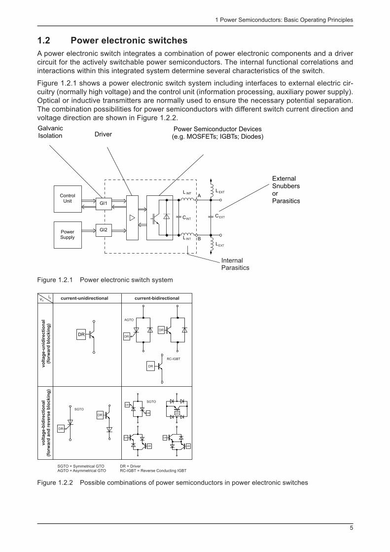
A power electronic switch integrates a combination of power electronic components and a driver circuit for the actively switchable power semiconductors. The internal functional correlations and interactions within this integrated system determine several characteristics of the switch.
Figure 1.2.1 shows a power electronic switch system including interfaces to external electric cir-cuitry (normally high voltage) and the control unit (information processing, auxiliary power supply). Optical or inductive transmitters are normally used to ensure the necessary potential separation. The combination possibilities for power semiconductors with different switch current direction and voltage direction are shown in Figure 1.2.2.
GalvanicIsolation Driver
Power Semiconductor Devices(e.g. MOSFETs; IGBTs; Diodes)
ControlUnit
PowerSupply
GI1
GI2
A
B
L
L
L
L
INT EXT
CC
ExternalSnubbersorParasitics
InternalParasitics
EXT
EXTINT
INT
Figure 1.2.1 Power electronic switch system
iSvScurrent-unidirectional current-bidirectional
AGTO
DR
DR
DR
RC-IGBT
SGTODR
DR DR
DR DR
DRDR
SGTO
DR
DR
vo
ltag
e-u
nid
irecti
on
al
(fo
rward
blo
ckin
g)
vo
ltag
e-b
idir
ecti
on
al
(fo
rward
an
d r
evers
e b
lockin
g)
SGTO = Symmetrical GTOAGTO = Asymmetrical GTO
DR = DriverRC-IGBT = Reverse Conducting IGBT
DR
Figure 1.2.2 Possible combinations of power semiconductors in power electronic switches
1 Power Semiconductors: Basic Operating Principles
6
On the one hand, the parameters of a complete switch result from the semiconductor switching be-haviour, which has to be adapted to the operating mode of the entire switch by way of semiconduc-tor chip design. On the other hand, the driver circuit is responsible for the main switch parameters and performs the key protection and diagnosis functions.
Basic types of power electronic switches
Owing to the operational principles of power semiconductors, which are clearly responsible for the dominant characteristics of the circuits in which they operate, power electronic switches may be split up into the following basic types. The main voltage and current directions clearly result from the requirements in the actual circuit, in particular from the injected currents and voltages in the commutation circuits.
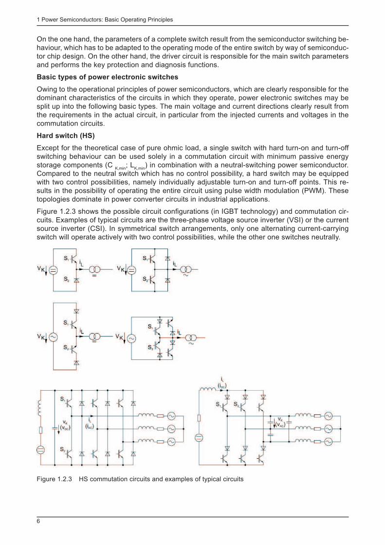
Hard switch (HS)
Except for the theoretical case of pure ohmic load, a single switch with hard turn-on and turn-off switching behaviour can be used solely in a commutation circuit with minimum passive energy storage components (C
K,min ; L
K,min ) in combination with a neutral-switching power semiconductor.
Compared to the neutral switch which has no control possibility, a hard switch may be equipped with two control possibilities, namely individually adjustable turn-on and turn-off points. This re-sults in the possibility of operating the entire circuit using pulse width modulation (PWM). These topologies dominate in power converter circuits in industrial applications.
Figure 1.2.3 shows the possible circuit confi gurations (in IGBT technology) and commutation cir-cuits. Examples of typical circuits are the three-phase voltage source inverter (VSI) or the current source inverter (CSI). In symmetrical switch arrangements, only one alternating current-carrying switch will operate actively with two control possibilities, while the other one switches neutrally.
Figure 1.2.3 HS commutation circuits and examples of typical circuits
1 Power Semiconductors: Basic Operating Principles
7
Zero current switch (ZCS)
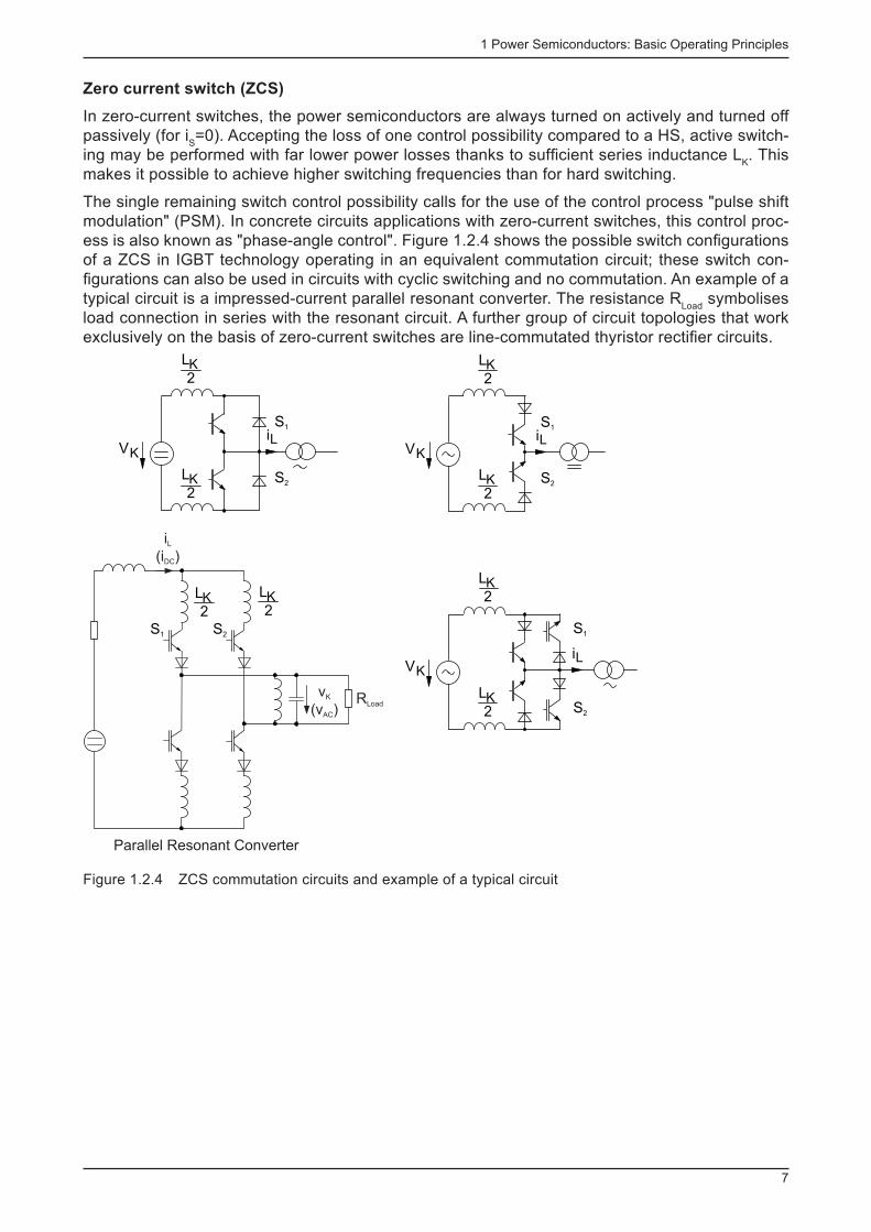
In zero-current switches, the power semiconductors are always turned on actively and turned off passively (for i
S =0). Accepting the loss of one control possibility compared to a HS, active switch-
ing may be performed with far lower power losses thanks to suffi cient series inductance L K . This
makes it possible to achieve higher switching frequencies than for hard switching.
The single remaining switch control possibility calls for the use of the control process "pulse shift modulation" (PSM). In concrete circuits applications with zero-current switches, this control proc-ess is also known as "phase-angle control". Figure 1.2.4 shows the possible switch confi gurations of a ZCS in IGBT technology operating in an equivalent commutation circuit; these switch con-fi gurations can also be used in circuits with cyclic switching and no commutation. An example of a typical circuit is a impressed-current parallel resonant converter. The resistance R
Load symbolises
load connection in series with the resonant circuit. A further group of circuit topologies that work exclusively on the basis of zero-current switches are line-commutated thyristor rectifi er circuits.
LK2
LK2
S2S1
RLoad
v
(v )K
AC
i
(i )L
DC
Parallel Resonant Converter
LK
VK
2
iL
LK2
S1
S2
VK
iL
LK2
LK2
S1
S2
VK
iL
LK2
LK2
S1
S2
Figure 1.2.4 ZCS commutation circuits and example of a typical circuit
1 Power Semiconductors: Basic Operating Principles
8
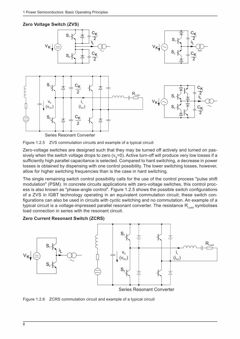
Zero Voltage Switch (ZVS)
iLVK
CK2
CK2
S1
S2
CK
2
CK
2
S1
S2
RLoad
v
(v )K
DC
i
(i )L
AC
Series Resonant Converter
CK
2iL
VK
CK
2
S1
S2
VK
iL
CK2
CK2
S2
S1
Figure 1.2.5 ZVS commutation circuits and example of a typical circuit
Zero-voltage switches are designed such that they may be turned off actively and turned on pas-sively when the switch voltage drops to zero (v
S =0). Active turn-off will produce very low losses if a
suffi ciently high parallel capacitance is selected. Compared to hard switching, a decrease in power losses is obtained by dispensing with one control possibility. The lower switching losses, however, allow for higher switching frequencies than is the case in hard switching.
The single remaining switch control possibility calls for the use of the control process "pulse shift modulation" (PSM). In concrete circuits applications with zero-voltage switches, this control proc-ess is also known as "phase-angle control". Figure 1.2.5 shows the possible switch confi gurations of a ZVS in IGBT technology operating in an equivalent commutation circuit; these switch con-fi gurations can also be used in circuits with cyclic switching and no commutation. An example of a typical circuit is a voltage-impressed parallel resonant converter. The resistance R
Load symbolises
load connection in series with the resonant circuit.
Zero Current Resonant Switch (ZCRS)
VK
iL
S1
S2
S1
S2
RLoad
v
(v )K
DC
i
(i )L
AC
Series Resonant Converter
Figure 1.2.6 ZCRS commutation circuit and example of a typical circuit
1 Power Semiconductors: Basic Operating Principles
9
A zero-current resonant switch is controlled such that active turn-on begins at the very moment at which the current i
L displays zero crossing. Thus, actual current commutation does not take place.
Consequently, even if there is a minimum commutation inductance L K , the turn-on losses are lower
than in zero-current switches and are caused by the necessary change in charge of the junction capacitances of the given power semiconductors. At the same time, the further power loss reduc-tion compared to ZCS means another loss of controllability, since the turn-on moment is not con-trollable, but is triggered by the zero-current crossing given by the outer circuitry. In circuits with ZCRS, only indirect control of the energy fl ow is possible and is done by conducting and blocking the switches across several periods of alternating current. This is referred to as pulse density modulation (PDM) or even pulse group modulation.
Figure 1.2.6 shows a commutation circuit with ZCRS, as well as a sample circuit in IGBT tech-nology. For ideal switching at zero crossing of alternating current, the switches would not need antiparallel switch diodes for the second current direction. In practice, however, these are included owing to non-ideal behaviour. The resistance R
Load symbolises load connection in series with the
resonant circuit.
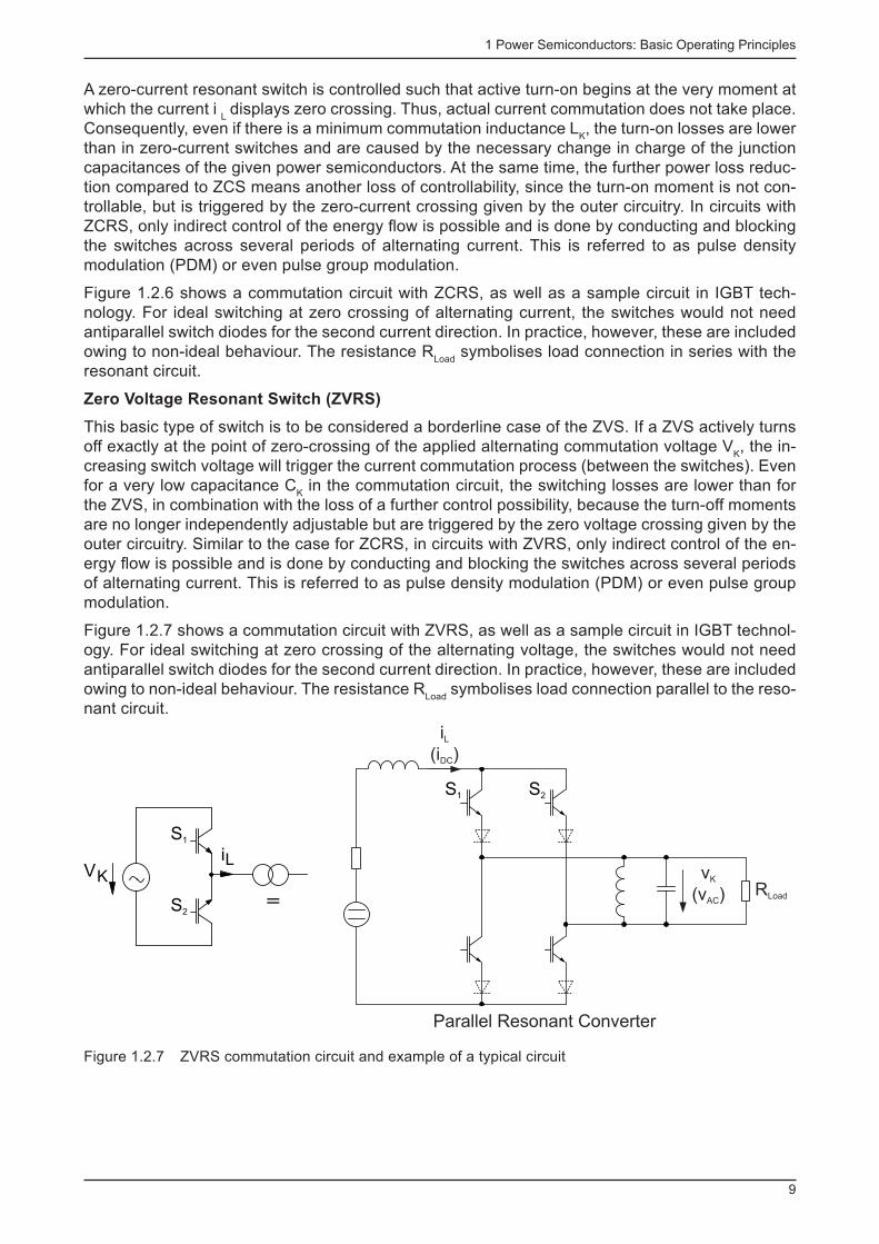
Zero Voltage Resonant Switch (ZVRS)
This basic type of switch is to be considered a borderline case of the ZVS. If a ZVS actively turns off exactly at the point of zero-crossing of the applied alternating commutation voltage V
K , the in-
creasing switch voltage will trigger the current commutation process (between the switches). Even for a very low capacitance C
K in the commutation circuit, the switching losses are lower than for
the ZVS, in combination with the loss of a further control possibility, because the turn-off moments are no longer independently adjustable but are triggered by the zero voltage crossing given by the outer circuitry. Similar to the case for ZCRS, in circuits with ZVRS, only indirect control of the en-ergy fl ow is possible and is done by conducting and blocking the switches across several periods of alternating current. This is referred to as pulse density modulation (PDM) or even pulse group modulation.
Figure 1.2.7 shows a commutation circuit with ZVRS, as well as a sample circuit in IGBT technol-ogy. For ideal switching at zero crossing of the alternating voltage, the switches would not need antiparallel switch diodes for the second current direction. In practice, however, these are included owing to non-ideal behaviour. The resistance R
Load symbolises load connection parallel to the reso-
nant circuit.
S1
RLoad
v
(v )K
AC
i
(i )L
DC
Parallel Resonant Converter
S2
VK
iL
=
S1
S2
Figure 1.2.7 ZVRS commutation circuit and example of a typical circuit
1 Power Semiconductors: Basic Operating Principles
10
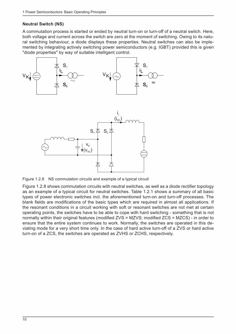
Neutral Switch (NS)
A commutation process is started or ended by neutral turn-on or turn-off of a neutral switch. Here, both voltage and current across the switch are zero at the moment of switching. Owing to its natu-ral switching behaviour, a diode displays these properties. Neutral switches can also be imple-mented by integrating actively switching power semiconductors (e.g. IGBT) provided this is given "diode properties" by way of suitable intelligent control.
v
(v )K
AC
S1 S2
i
(i )L
DC
VK
iLVK
iL
=
S1
S2S2
S1
S2S2
Figure 1.2.8 NS commutation circuits and example of a typical circuit
Figure 1.2.8 shows commutation circuits with neutral switches, as well as a diode rectifi er topology as an example of a typical circuit for neutral switches. Table 1.2.1 shows a summary of all basic types of power electronic switches incl. the aforementioned turn-on and turn-off processes. The blank fi elds are modifi cations of the basic types which are required in almost all applications. If the resonant conditions in a circuit working with soft or resonant switches are not met at certain operating points, the switches have to be able to cope with hard switching - something that is not normally within their original features (modifi ed ZVS = MZVS; modifi ed ZCS = MZCS) - in order to ensure that the entire system continues to work. Normally, the switches are operated in this de-viating mode for a very short time only. In the case of hard active turn-off of a ZVS or hard active turn-on of a ZCS, the switches are operated as ZVHS or ZCHS, respectively.

1 Power Semiconductors: Basic Operating Principles
11
hard soft
L K in series
resonant
i L = 0
neutral
V S = 0
hard HS MZCS ZVHS
softC
K in parallel
MZVS ZVS
resonantV
K = 0
ZVRS
neutrali S = 0
ZCHS ZCS ZCRS NS
Table 1.2.1 Basic types of power electronic switches
OFF
ON

1 Power Semiconductors: Basic Operating Principles
12
2 Basics
13
2 Basics
2.1 Application fi elds and current performance limits for power
semiconductors
The development of power semiconductors saw the onset of lasting success for power electronics across all fi elds of electrical engineering. Given the ever increasing call for resource conservation (e.g. energy saving agenda), the use of renewable energies (e.g.wind power and photovoltaics) and the need for alternatives to fossil fuels (e.g. electric and hybrid drives for vehicles), this suc-cess is gaining more and more momentum today.
This development is also largely driven by the interactions between system costs and market pen-etration, as well as the energy consumption required for production and the energy saving poten-tial of products in operation. In addition to the general aim to expand the performance profi le, the development aims "low materials consumption/ low costs" and "high effi ciency" are gaining more and more importance.
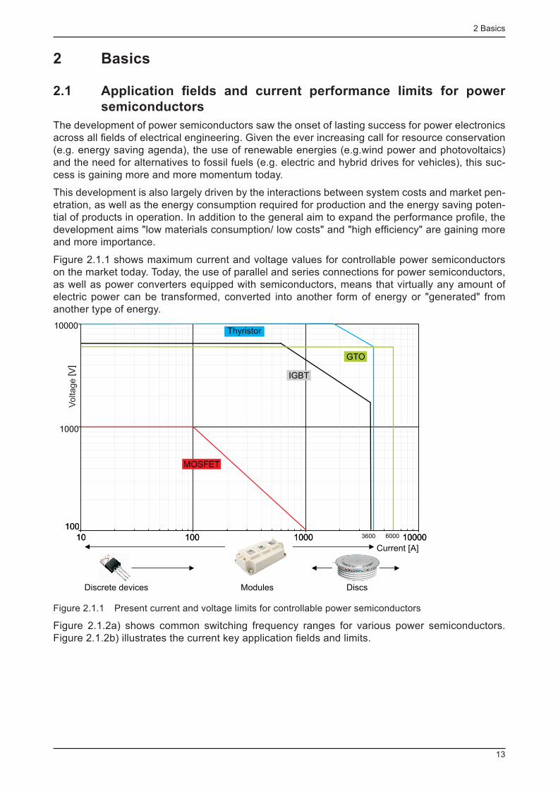
Figure 2.1.1 shows maximum current and voltage values for controllable power semiconductors on the market today. Today, the use of parallel and series connections for power semiconductors, as well as power converters equipped with semiconductors, means that virtually any amount of electric power can be transformed, converted into another form of energy or "generated" from another type of energy.
100
1000
10000
10 100 1000 10000
100
10 100 1000 10000
[ V]
MOSFET
IGBT
GTO
Thyristor
3600 6000
Current [A]
Discrete devices Modules Discs
Voltage
Figure 2.1.1 Present current and voltage limits for controllable power semiconductors
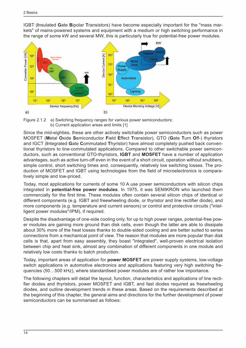
Figure 2.1.2a) shows common switching frequency ranges for various power semiconductors. Figure 2.1.2b) illustrates the current key application fi elds and limits.
2 Basics
14
IGBT ( I nsulated G ate B ipolar T ransistors) have become especially important for the "mass mar-kets" of mains-powered systems and equipment with a medium or high switching performance in the range of some kW and several MW, this is particularly true for potential-free power modules.
Figure 2.1.2 a) Switching frequency ranges for various power semiconductors; b) Current application areas and limits [1]
Since the mid-eighties, these are other actively switchable power semiconductors such as power MOSFET ( M etal O xide S emiconductor F ield E ffect T ransistor), GTO ( G ate T urn O ff-) thyristors and IGCT ( I ntegrated G ate C ommutated T hyristor) have almost completely pushed back conven-tional thyristors to line-commutated applications. Compared to other switchable power semicon-ductors, such as conventional GTO-thyristors, IGBT and MOSFET have a number of application advantages, such as active turn-off even in the event of a short circuit, operation without snubbers, simple control, short switching times and, consequently, relatively low switching losses. The pro-duction of MOSFET and IGBT using technologies from the fi eld of microelectronics is compara-tively simple and low-priced.
Today, most applications for currents of some 10 A use power semiconductors with silicon chips integrated in potential-free power modules . In 1975, it was SEMIKRON who launched them commercially for the fi rst time. These modules often contain several silicon chips of identical or different components (e.g. IGBT and freewheeling diode, or thyristor and line rectifi er diode), and more components (e.g. temperature and current sensors) or control and protective circuits ("intel-ligent power modules"/IPM), if required.
Despite the disadvantage of one-side cooling only, for up to high power ranges, potential-free pow-er modules are gaining more ground than disk cells, even though the latter are able to dissipate about 30% more of the heat losses thanks to double-sided cooling and are better suited to series connections from a mechanical point of view. The reason that modules are more popular than disk cells is that, apart from easy assembly, they boast "integrated", well-proven electrical isolation between chip and heat sink, almost any combination of different components in one module and relatively low costs thanks to batch production.
Today, important areas of application for power MOSFET are power supply systems, low-voltage switch applications in automotive electronics and applications featuring very high switching fre-quencies (50…500 kHz), where standardised power modules are of rather low importance.
The following chapters will detail the layout, function, characteristics and applications of line recti-fi er diodes and thyristors, power MOSFET and IGBT, and fast diodes required as freewheeling diodes, and outline development trends in these areas. Based on the requirements described at the beginning of this chapter, the general aims and directions for the further development of power semiconductors can be summarised as follows:

2 Basics
15
The key aims for further development are as follows: - Increasing the switching performance (current, voltage) - Reducing losses in the semiconductors as well as in control and protective circuits - Expanding the operating temperature range - Improved service life, ruggedness and reliability - Reducing the amount of control and protection required; improving component behaviour in the event of error / failure
- Cost reduction
The development directions can be broken down as follows:
Semiconductor materials
- New semiconductor materials (e.g. wide bandgap materials)
Chip technology
- Higher permissible chip temperatures or current densities (reduction of chip area) - Finer structures (reduction of chip area) - New structures (improvement of chip characteristics) - Integration of functions on the chip (e.g. gate resistance, temperature measurement, monolithic system integration)
- New monolithic components by combining functions (RC-IGBT, ESBT) - Improved stability of chip characteristics under different climatic conditions
Packaging
- Increase in thermal and power cycling capability - Improvement of heat dissipation (isolation substrate, base plate, heat sink) - Wider scope of application as regards climate conditions thanks to improvements in casing and potting materials or new packaging concepts
- Optimisation of internal connections and connection layouts regarding parasitic elements - User-friendly package optimisation to simplify device construction - Reduction of packaging costs and improvement of environmental compatibility in production, operation and recycling
Degree of integration
- Increasing the complexity of power modules to reduce system costs - Integration of driver, monitoring and protective functions - System integration
Figure 2.1.3 shows different power module integration levels
Module concept:Power semiconductor soldered and bonded
Sub- IPM +
Controller +
bus interfaces
Standard
modulesSwitching,
Insulation
Modules +
Driver +
Protection
SolderChip
Bond wireModule concept:
Power semiconductor soldered and bonded
IPM +
Controller +
bus interfacessystems
IPM +
Controller +
bus interfaces
Switching,
Insulation
Switches,
Insulation
Modules +
Driver +
ProtectionIPM
Modules +
Driver +
Protection
SolderChip
Bond wire
Figure 2.1.3 Power module integration levels
2 Basics
16
More complex technologies, smaller semiconductor structures and precise process control are inevitably driving the properties of modern power semiconductors towards the physical limits of silicon. For this reason, research into alternative semiconductor materials, which began as early as the 1950s, was pushed in recent years and has since resulted in the fi rst mass products.
Today, the " wide bandgap materials " silicon carbide (SiC) and gallium nitride (GaN) are the main focus of this research. Compared to silicon, they display a far higher energetic gap between va-lence and conduction band, resulting in comparatively lower forward on-state losses and switching losses, higher permissible chip temperatures, and better heat conductivity than silicon.
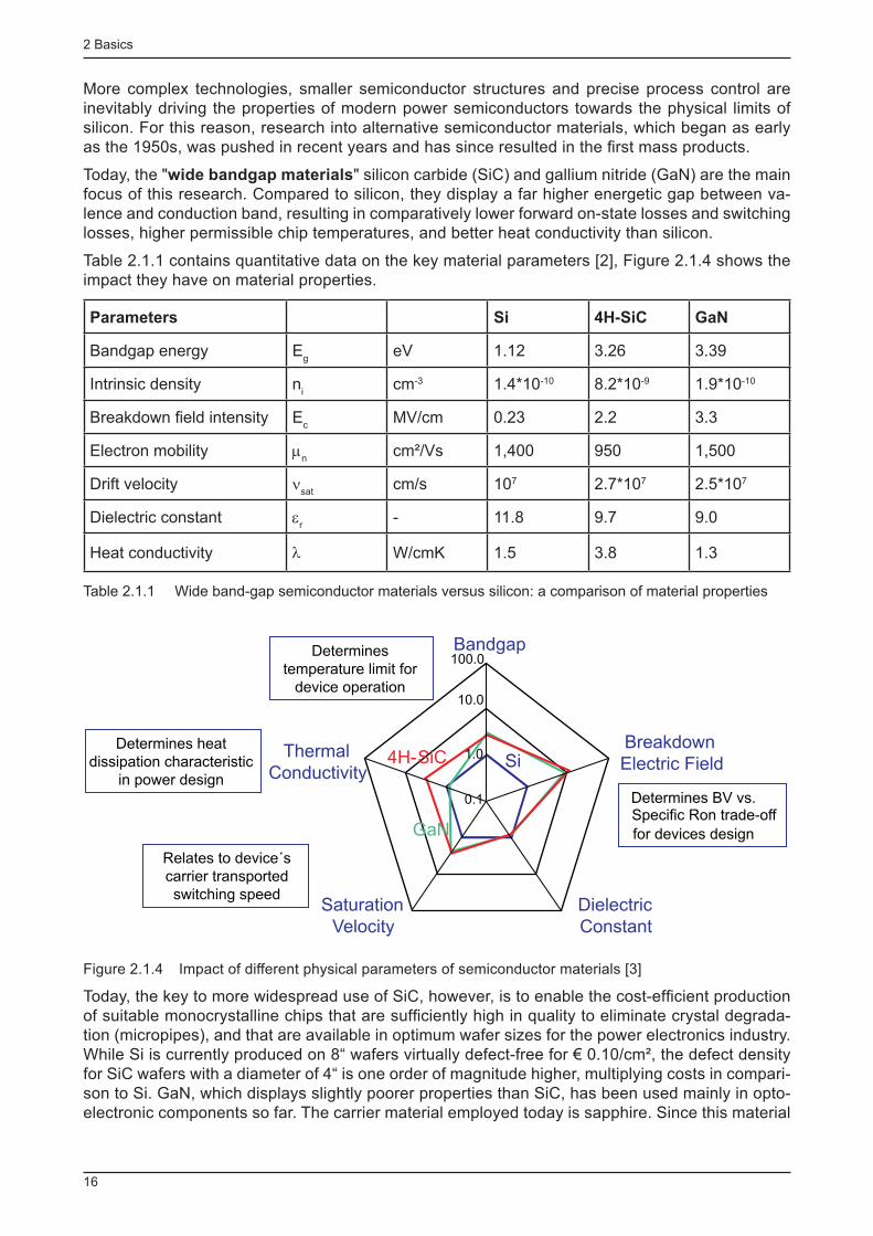
Table 2.1.1 contains quantitative data on the key material parameters [2], Figure 2.1.4 shows the impact they have on material properties.
Parameters Si 4H-SiC GaN
Bandgap energy E g
eV 1.12 3.26 3.39
Intrinsic density n i
cm -3 1.4*10 -10 8.2*10 -9 1.9*10 -10
Breakdown fi eld intensity E c
MV/cm 0.23 2.2 3.3
Electron mobility µ n
cm²/Vs 1,400 950 1,500
Drift velocity ν sat
cm/s 10 7 2.7*10 7 2.5*10 7
Dielectric constant ε r
- 11.8 9.7 9.0
Heat conductivity λ W/cmK 1.5 3.8 1.3
Table 2.1.1 Wide band-gap semiconductor materials versus silicon: a comparison of material properties
Dielectric
Constant
Breakdown
Electric Field
Bandgap
Thermal
Conductivity
Saturation
Velocity
Determines
temperature limit for
device operation
Determines BV vs.Specific Ron trade-off
for devices designGaN
4H-SiC Si
Relates to device´s
carrier transported
switching speed
Determines heat
dissipation characteristic
in power design
100.0
10.0
1.0
0.1
Figure 2.1.4 Impact of different physical parameters of semiconductor materials [3]
Today, the key to more widespread use of SiC, however, is to enable the cost-effi cient production of suitable monocrystalline chips that are suffi ciently high in quality to eliminate crystal degrada-tion (micropipes), and that are available in optimum wafer sizes for the power electronics industry. While Si is currently produced on 8“ wafers virtually defect-free for € 0.10/cm², the defect density for SiC wafers with a diameter of 4“ is one order of magnitude higher, multiplying costs in compari-son to Si. GaN, which displays slightly poorer properties than SiC, has been used mainly in opto-electronic components so far. The carrier material employed today is sapphire. Since this material
2 Basics
17
is non-conductive, GaN components must have planar structures. The most common type of diode on the market today is the SiC Schottky diode.
Owing to the advanced development stage of Si power semiconductors, there is no technical need to introduce other semiconductor materials for MOSFET and IGBT in the voltage range < 1000 V. In this voltage range, wide bandgap semiconductor materials are more likely to be competitive in junction-gate driven power semiconductors such as JFET (junction gate fi eld-effect transistors), bipolar transistors and thyristors, whereas MOS-driven transistors clearly outplay silicon compo-nents when higher voltages are applied.
Owing to high material costs, power semiconductors made of "wide bandgap materials" are used fi rst and foremost in applications where a particularly high effi ciency ratio or minimum absolute losses are required, as well as in applications whose requirements – e.g. temperature, voltage or frequency – cannot be met with Si power semiconductors.
In order to to fully benefi t from the main advantages that power semiconductors made of SiC or GaN have over conventional components, such as - low conduction and switching losses - higher blocking voltages - higher possible power densities - higher permissible operating temperatures - shorter switching times, higher switching frequencies,
it is vital for packaging to be further developed and improved on accordingly.
2.2 Line rectifi ers
2.2.1 Rectifi er diodes
Circuit symbol
Anode
Cathode
2.2.1.1 General terms
Forward direction
Direction of current fl ow where the rectifi er diode has the lower resistance.
Reverse direction
Direction of current fl ow where the rectifi er diode has the higher resistance.
Anode terminal
Terminal into which the forward current (on-state current) fl ows.
Cathode terminal
Terminal out of which the forward current (on-state current) fl ows.
On-state current (forward current)
Current fl owing in forward direction.
On-state voltage (forward voltage)
Voltage applied between the terminals as a result of the forward current.

2 Basics
18
Reverse current
Current fl owing in reverse direction as a result of blocking voltage (reverse voltage). If the off-state current is displayed using a plotter, an oscilloscope or a similar measuring instrument with a screen, DC voltage should be used for measurements if possible. If measurements are taken us-ing AC voltage, it is important to note that the capacitance of the pn-junction causes a split in the characteristic curve. Depending on the rising or falling voltage, there will be a positive or negative displacement current which splits the characteristic into two branches. The point in the peak of the measurement voltage is not distorted by capacitive infl uences and shows the true reverse current (Figure 2.2.1).
measured voltage v
reversecurrent i
reverse current i at vr r
capacitive hysteresis
vr
Figure 2.2.1 Blocking characteristic with capacitive splitting as a result of AC measurements.
Blocking voltage (reverse voltage)
Voltage applied between the terminals in reverse direction
2.2.1.2 Structure and functional principle
Rectifi er diodes are components with two terminals and are used to rectify alternating currents. They have an asymmetrical current-voltage characteristic (Figure 2.2.2).
Conducting area
Threshold voltage
Forward direction
Reverse
direction
Blocking areaBreak through
Equivalent slope
resistance
V
I
Figure 2.2.2 Current-voltage characteristic of a rectifi er diode with voltage directions, current/voltage areas and equivalent resistance line
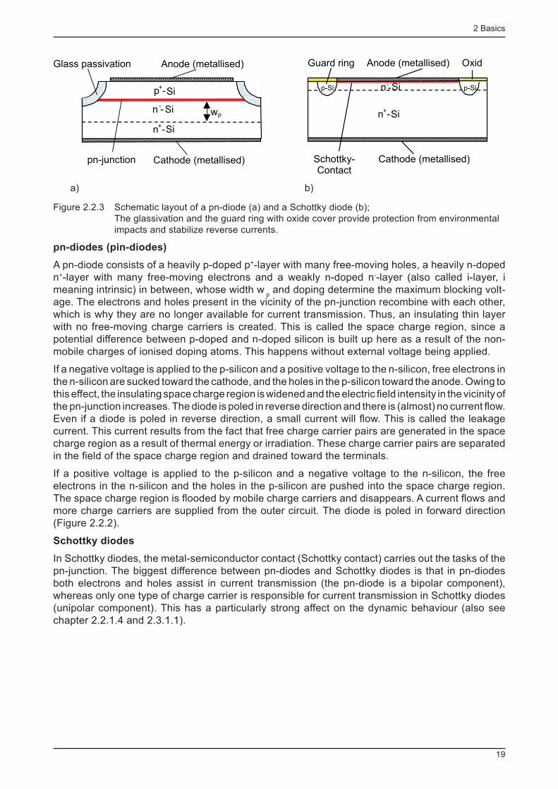
Today, the semiconductor diodes used to rectify line voltages are produced mainly on the basis of monocrystalline silicon. A distinction is made between diodes whose rectifying effect is caused by the transition of mobile charge carriers from an n-doped to a p-doped area in the semiconductor ( pn-diodes ) and Schottky diodes , where a metal-semiconductor junction produces the rectifying effect.
2 Basics
19
Anode (metallised)
p+-Si
n--Si
n+-Si
Glass passivation
pn-junction Cathode (metallised)
wp
Anode (metallised)
n--Si
n+-Si
Guard ring
Schottky-Contact
Cathode (metallised)
p-Si
Oxid
p-Si
a) b)
Figure 2.2.3 Schematic layout of a pn-diode (a) and a Schottky diode (b);The glassivation and the guard ring with oxide cover provide protection from environmental impacts and stabilize reverse currents.
pn-diodes (pin-diodes)
A pn-diode consists of a heavily p-doped p + -layer with many free-moving holes, a heavily n-doped n + -layer with many free-moving electrons and a weakly n-doped n - -layer (also called i-layer, i meaning intrinsic) in between, whose width w
p and doping determine the maximum blocking volt-
age. The electrons and holes present in the vicinity of the pn-junction recombine with each other, which is why they are no longer available for current transmission. Thus, an insulating thin layer with no free-moving charge carriers is created. This is called the space charge region, since a potential difference between p-doped and n-doped silicon is built up here as a result of the non-mobile charges of ionised doping atoms. This happens without external voltage being applied.
If a negative voltage is applied to the p-silicon and a positive voltage to the n-silicon, free electrons in the n-silicon are sucked toward the cathode, and the holes in the p-silicon toward the anode. Owing to this effect, the insulating space charge region is widened and the electric fi eld intensity in the vicinity of the pn-junction increases. The diode is poled in reverse direction and there is (almost) no current fl ow. Even if a diode is poled in reverse direction, a small current will fl ow. This is called the leakage current. This current results from the fact that free charge carrier pairs are generated in the space charge region as a result of thermal energy or irradiation. These charge carrier pairs are separated in the fi eld of the space charge region and drained toward the terminals.
If a positive voltage is applied to the p-silicon and a negative voltage to the n-silicon, the free electrons in the n-silicon and the holes in the p-silicon are pushed into the space charge region. The space charge region is fl ooded by mobile charge carriers and disappears. A current fl ows and more charge carriers are supplied from the outer circuit. The diode is poled in forward direction (Figure 2.2.2).
Schottky diodes
In Schottky diodes, the metal-semiconductor contact (Schottky contact) carries out the tasks of the pn-junction. The biggest difference between pn-diodes and Schottky diodes is that in pn-diodes both electrons and holes assist in current transmission (the pn-diode is a bipolar component), whereas only one type of charge carrier is responsible for current transmission in Schottky diodes (unipolar component). This has a particularly strong affect on the dynamic behaviour (also see chapter 2.2.1.4 and 2.3.1.1).
2 Basics
20
2.2.1.3 Static behaviour
On-state behaviour
When forward voltage is applied, the current will increase steeply as soon as the threshold volt-
age for silicon this is approx. 0.7 V) has been reached (Figure 2.2.2). Only at very high currents which are far above the permissible continuous current will this on-state curve level out slightly. For low and medium currents, the temperature coeffi cient of the on-state voltage is negative, which means that, at constant current, the higher the temperature, the lower the on-state volt-age. With very high currents this behaviour is reversed. When the on-state current fl ows, on-state losses are created (= on-state current * on-state voltage), heating up the diode. This heat build-up limits the forward current, since excessive heat may damage the diode.
Blocking behaviour
If voltage is applied to a diode in reverse direction, the reverse current will initially rise until it reaches a level - at just a few volts - which will barely increase further as the voltage is increased. The reverse current is highly temperature-dependent and rises proportionate to temperature, an effect that is particularly strong in the case of Schottky diodes. Under normal operating conditions, however, the losses that occur (= blocking voltage * reverse current) are so small that they can be neglected when calculating the overall losses (exception: Schottky diodes). If the voltage applied in reverse direction is increased until it reaches the breakdown region (Figure 2.2.2), the reverse current will rise more or less steeply. Two mechanisms may cause this rise: the Zener effect and the avalanche effect.
Zener effect
In diodes with a very highly doped n - middle region, the fi eld intensity in the space charge region may become so high that electrons are snatched away from the silicon atom bonds, thus creating free charge carrier pairs (Zener effect). This causes the reverse current to rise very steeply. The Zener voltage which is present when this rise occurs drops as the temperature increases. The Zener effect appears only in combination with extremely high fi eld intensities in the space charge region. Such fi eld intensities are only observed in diodes with a relatively low breakdown voltage. The limit is 5.7 V. In the case of higher breakdown voltages, this effect is known as the avalanche effect.
Avalanche effect
Within the space charge region, free charge carriers (electrons or holes) are generated as a re-sult of thermal or optical energy. In the avalanche effect, these charge carriers are accelerated by the electric fi eld intensity prevailing in the space charge region to such an extent that, due to their kinetic energy, they may create more charge carrier pairs by bumping into valence electrons (ionisation by collision). The number of free charge carriers increases like an avalanche, which is also true for the reverse current. The avalanche voltage which is present when this effect ap-pears has a positive temperature coeffi cient, i.e. it increases proportionate to the temperature. All breakdown voltages greater than 5.7 V are caused by the avalanche effect. Avalanche diodes are often wrongly called Zener diodes. Operating a diode in avalanche breakdown is only permitted if explicitly specifi ed in the datasheet.
2.2.1.4 Dynamic behaviour
Turn-on behaviour
When the diode switches to conductive state, the voltage will initially increase to the maximum turn-on voltage V
FRM . Only when the n - -region has been completely fl ooded by charge carriers will
the on-state voltage drop to its static value V F (Figure 2.2.4). Forward recovery time t
fr is in the
range of 100 ns. The steeper the current rise and the thicker the low-doped n - -region in the diode, the higher V
FRM will be. The turn-on peak voltage may be 300 V and above.
2 Basics
21
tfr
static value of forwardvoltage
IF
0.1 IF
v
VF
F0.1 VF
1.1 VF
t
maximum turn-on voltageVFRM
Figure 2.2.4 Diode turn-on behaviour
Turn-off behaviour
pn-diodes
In conductive state, the entire volume of the diode is fl ooded with electrons and holes. If voltage polarity is then reversed, the diode will also conduct in reverse direction, meaning that no block-ing voltage can be built up. Owing to the reverse current and the recombination of electrons and holes, excess charge is depleted in the diode. As soon as all excess charge carriers are depleted to zero at the pn-junction, the diode can take up blocking voltage again, the peak reverse recovery current I
RRM is reached, and from this point on the reverse current will decline again (Figure 2.2.5).
Figure 2.2.5 Turn-off behaviour of a pn-diode: defi nitions (a) and current curve, voltage and switching losses (b)
The red triangle Q rr is the charge stored in the diode. When the peak reverse recovery current I
RRM
has passed, voltage is present at the diode and a current fl ows through it. This results in switch-ing losses, which may reach considerable levels when higher frequencies are applied and must be taken into account in the total losses. Reverse recovery time t
rr , storage charge Q
rr and peak
reverse recovery current I RRM
increase strongly at higher temperatures. Diodes with a short reverse recovery time t
rr , small storage charge Q
rr and low peak reverse recovery current I
RRM are called
fast diodes (see chapter 2.3). Fast diodes are obtained by reducing the carrier life, for example.

2 Basics
22
Schottky diodes
Schottky diodes are unipolar components; only one type of charge carrier is responsible for cur-rent transmission. While the on-state current is fl owing, no excess charge which could appear as storage charge when the diode is turned off (reversed polarity) is built up. This means that Schottky diodes have no reverse current I
RRM , apart from a very low current for recharging the junc-
tion capacitance. A reverse recovery time is not defi ned.
Owing to their minimal switching losses, Schottky diodes are highly suitable for use in high-fre-quency applications. Their blocking voltages, however, are limited due to the reverse currents which rise steeply when the temperature rises and the unipolar on-state character. Silicon-based Schottky diodes are currently available with a blocking voltage of up to around 200 V; those made of gallium arsenide (GaAs) are suitable for up to 300 V, while Schottky diodes made of silicon car-bide (SiC) are available for up to 1200 V. The suitability of SiC for high-blocking Schottky diodes is down to the material's breakdown fi eld intensity, which is nine times higher than silicon.
2.2.2 Thyristors
Circuit symbol
Anode
Cathode
Gate
2.2.2.1 General terms
Forward direction, switching direction
The direction of current fl ow through the main terminals in which the thyristor can assume two stable operating states, i.e. off-state and on-state.
Reverse direction
The direction opposite to switching direction.
On-state
Operating state at a certain operating point or operating point range where the DC resistance is small (compared to the resistance in off-state).
Off-state
Operating state where the DC resistance is high (compared to the resistance in on-state).
Anode terminal
Main terminal where the forward current enters the thyristor.
Cathode terminal
Main terminal where the forward current leaves the thyristor.
Gate
Terminal through which only gate current fl ows. The device intended for control is connected to the gate and the cathode terminal. For this purpose, larger thyristors are equipped with a second cathode terminal.
Forward current
The current fl owing in forward direction through the main terminals.

2 Basics
23
Reverse current
The current fl owing in reverse direction through the main terminals.
On-state current
The current fl owing through the main terminals in on-state.
Off-state current
The current fl owing through the main terminals in off-state. If the off-state current is displayed us-ing a plotter, an oscilloscope or a similar measuring instrument with a screen, DC voltage should be used for measurements if possible. If measurements are taken using AC voltage, it is important to note that the capacitance of the pn-junction causes a split in the characteristic curve. Depend-ing on the rising or falling voltage, there will be a positive or negative displacement current which splits the characteristic into two branches. The point in the peak of the measurement voltage is not distorted by capacitive infl uences and shows the true reverse current (see Figure 2.2.1).
Forward voltage
Voltage applied at the main terminals in forward direction.
Reverse voltage
Voltage applied at the main terminals in reverse direction.
On-state voltage
Voltage applied at the main terminals in on-state.
Reverse voltage
Voltage applied at the main terminals in off-state.
Breakover voltage
Blocking voltage in forward direction, where the thyristor suddenly transits into on-state without gate current fl owing.
Gate current
The current fl owing through the gate. This is called positive when it fl ows into the gate.
Gate voltage
Voltage between gate and cathode terminal. This is known as positive if the gate has the higher potential.
2.2.2.2 Structure and functional principle
A thyristor is a semiconductor component with a minimum of 3 pn-junctions which can be switched from off-state to on-state. Often, "thyristor" specifi cally designates the reverse-blocking triode thy-ristor which cannot be switched in reverse direction but blocks. In addition to the two terminals that a diode provides, a thyristor has a gate which serves to switch the thyristor to the on-state (Figure 2.2.6).
2 Basics
24
Forwardblocking
Forward breakover
Forward direction
Conducting
Reverseblocking
Break throughvoltage Holding
current
Reverse direction
I
V
Figure 2.2.6 Current-voltage characteristic of a thyristor with voltage directions and operating states.
p-Si
n--Si
n+ -Si
Glass passivation
Cathode (metallised)
p+-Si
Gate (metallised)
High blocking pn-junction
Low blocking pn-junction
Anode (metallised)
Figure 2.2.7 Diagram of a thyristor (glassivation acts as protection from environmental impacts and stabi-lizes reverse currents).
A thyristor consists of four alternate n-doped and p-doped regions (Figure 2.2.7). Together with the adjacent p-doped regions, the middle n - -region forms the high-blocking pn-junctions in forward and reverse direction. Passiviation (here: glassivation) must be performed for both pn-junctions. In order to be able to understand how a thyristor works, you can fi rst imagine the thyristor divided into an NPN transistor and a PNP transistor (Figure 2.2.8)
n
n
p
p
Cathode
Anode
Gate
n
p
n
p
Gate
Cathode
Anode
n
pGate
Cathode
Anode
Figure 2.2.8 Splitting a thyristor into two coupled NPN and PNP transistors
If the cathode is negatively polarized with respect to the anode, a current will fl ow from the gate to the cathode; as a result, the cathode, which is the emitter of the NPN transistor, will inject elec-trons. The gate current is amplifi ed by the NPN transistor. Some of these electrons will reach the low-doped region which simultaneously acts as collector of the NPN transistor and basis of PNP transistor. In the PNP transistor, this current is further amplifi ed and conducted to the basis of the NPN transistor. This coupling of the transistor parts is crucial for the functioning of the thyristor.
2 Basics
25
The current amplifi cation in the transistor is current-dependent. As soon as the current in the gate region becomes so high that the sum of current gains (in basis circuit) results in α
npn + α
pnp ≥ 1, the
current is amplifi ed beyond all measure and the thyristor is triggered, meaning it turns into an on-state. A short current pulse to the gate (e.g. lasting 10 µs) is suffi cient to trigger the thyristor. If the main current has exceeded the latching current I
L at the end of the trigger pulse, the thyristor will
stay in on-state. Only if the main current falls below the holding current I H will the thyristor switch
back to forward off-state (blocking state) (see chapter 2.2.2.3). Every current fl owing through the pn-junction from the gate to the cathode acts as trigger current if it is high enough: - External trigger current from gate to cathode - Off-state current by exceeding the maximum blocking voltage (breakover voltage) ("break-over triggering")
- Current generated in the space charge region by light incidence (light triggering) - Excessive temperature (thermally generated off-state current) - Capacitive displacement current owing to steeply rising anode voltage (dv/dt).
2.2.2.3 Static behaviour
On-state behaviour
The on-state behaviour of thyristors corresponds to that of diodes. When forward voltage is ap-plied, current will increase steeply as soon as the threshold voltage has been reached (Figure 2.2.6). Only at very high currents which are far above the permissible continuous current will this on-state curve level out slightly. For low and medium currents, the temperature coeffi cient of the on-state voltage is negative, which means that, at constant current, the higher the tem-perature, the lower the on-state voltage. With very high currents this behaviour is reversed. When the on-state current fl ows, on-state losses are created (= on-state current * on-state volt-age), heating up the thyristor. This heat build-up limits the forward current, since excessive heat might damage the thyristor.
Blocking behaviour
If voltage is applied to a thyristor in reverse direction , the off-state current will initially rise until it reaches a level - at just a few volts - which will barely increase further as the voltage is in-creased. The off-state current is highly temperature-dependent and increases in proportion to the temperature. If the voltage applied in reverse direction is increased until it reaches the breakdown region (Figure 2.2.6), the off-state current will rise steeply as a result of the avalanche effect (see chapter 2.2.1.3).
If voltage is applied to a thyristor in forward direction , it initially behaves as it would if voltage were applied in reverse direction. If breakover voltage is reached, the thyristor will suddenly transit into on-state and stay in this condition until this value falls below the latching current. Forward off-state voltage is also temperature-dependent. This dependence can vary greatly from one thyris-tor to another. At high temperatures, the forward off-state current is often higher than in reverse direction. The reason for this is usually the off-state current gain from the NPN transistor for which this off-state current is a base current. High forward off-state currents do not limit the functionality and reliability of thyristors; they do not constitute a quality impairing characteristic. Under normal operating conditions, the losses that occur (= blocking voltage * off-state current) are so small that they can be neglected when calculating the overall losses.
2 Basics
26
2.2.2.4 Dynamic behaviour
Turn-on behaviour
Firing by way of an external trigger current from gate to cathode
Thyristor fi ring starts locally at the point where the highest trigger current density is present. The triggered area spreads relatively slowly (depending on the conditions, at a rate of between 30 µm and 100 µm per µs), meaning that for a thyristor diameter of 100 mm, it will take some 1,000 mi-croseconds for the entire thyristor surface to become conductive (Figure 2.2.9).
Figure 2.2.9 Current distribution in the thyristor after gate current turn-on (a) and immediately after fi ring (b)
After the thyristor has been fi red, the forward voltage will drop very slowly to the static value V F .
This results in a power loss peak which grows in proportion to the current rise slope (Figure 2.2.10).
i
v
t
t
VA
V,I
IF
P
VF
PF
a)
b)
Figure 2.2.10 Current and voltage curves (a) and losses (b) during thyristor turn-on.
Since the area fi red initially is very small, the turn-on losses caused by the gradual decline of the on-state voltage to its static value V
F are concentrated on a small area. This causes the silicon to
heat up locally. In order to avoid damage to the thyristor, the rate of current rise must be limited to the maximum permissible critical rate of current rise (di/dt)
cr .
For larger thyristors, the critical rate of current rise (di/dt) cr is increased by integrating an auxiliary
thyristor (pilot thyristor). Here, a smaller thyristor whose cathode is connected to the gate of the main thyristor serves to amplify the trigger current for the main thyristor (Figure 2.2.11). The trigger energy for the main thyristor is taken from the main circuit. This is called internal turn-on amplifi ca-tion or amplifying gate-thyristor .
2 Basics
27
Hybrid auxiliary thyristor Integrated auxiliary thyristor
Gate
Main thyristor
Finger like auxiliary thyristor
Auxiliarythyristor
Figure 2.2.11 Trigger energy amplifi cation using an auxiliary thyristor (amplifying gate).
The ratio of (di/dt) cr is further improved by the fi nger-shaped amplifying gate which extends the
edge length between auxiliary and main thyristor. A shortcoming of this, however, is that the active emitter area is reduced, as is the current carrying capacity.
Thyristor fi ring using capacitive displacement current (dv/dt fi ring)
Every pn-junction is a voltage-dependent capacitance. This capacitance will be biggest if no volt-age is applied, and will drop as the blocking voltage applied is increased. Changes in voltage (high dv/dt) cause a capacitive displacement current to fl ow through the pn-junction. If this current is high enough, it can, like any other current through the p-base–emitter-junction, induce thyristor fi ring.
Triggering by exceeding the breakover voltage ("overhead fi ring")
If the breakover voltage is exceeded (Figure 2.2.12), the off-state current will become so high that it will fi re the thyristor. Since the off-state current rises in proportion to the temperature and the necessary trigger current decreases in proportion to the temperature, the breakover voltage will decline in proportion to the increase in temperature.
II
Forward break through
Reverse blocking
Conducting
Forward blockingVAK
Forward breakover voltage
Holding current
Figure 2.2.12 Triggering a thyristor by exceeding the breakover voltage
2 Basics
28
Triggering by light or excessive temperature
Light incidence creates charge carrier pairs which are separated in the space charge region and fl ow through the pn-junction to the cathode. They therefore act like a trigger current. The same is true for thermally generated charge carrier pairs.
Turn-off behaviour
As is the case for line rectifi er diodes (see chapter 2.2.1.4), the volume of a thyristor semiconduc-tor is also fl ooded by charge carriers when a forward current fl ows. The majority of these charge carriers have to be depleted when the voltage is reversed for the thyristor to be able to pick up voltage in reverse direction. That said, residual charge carriers will still be present in the semicon-ductor volume and these may cause thyristor fi ring if voltage is applied in forward direction.
The circuit commutated turn-off time t q refers to the time that elapses from the moment of zero-
current-crossing until the moment that blocking voltage can be re-applied without the thyristor re-fi ring (Figure 2.2.13). The typical t
q for thyristors is about 100 to 500 µs. Fast thyristors (fre-
quency thyristors) are thyristors where the circuit commutated turn-off time has been shortened to between 10 and 100 µs by reducing the carrier life. More details on the dependency of the circuit commutated turn-off time on the parameters can be found in chapter 3.2.5.2. The characteristics are explained in chapter 3 "Datasheet parameters".
tq
t
i, v
Current iT
Voltage vT
Figure 2.2.13 Current i T and voltage v
T curves of a thyristor during turn-off and circuit commutated recov-
ery time t q
2.3 Freewheeling and snubber diodes
2.3.1 Structure and functional principle
Modern fast switching devices require fast diodes as freewheeling diodes in the power circuit. In the predominant applications which use inductive loads, the freewheeling diode is commutated from conductive to blocking state with every turn-on operation of the switch. Here, storage charges are to be depleted gently in order to avoid induced voltage spikes and high-frequency oscillations. For this reason, these diodes are also referred to as soft-recovery diodes. They are also instru-mental to switch performance. When designing these devices, a compromise between confl icting requirements has to be found. Two main types of fast diodes exist: the Schottky diode, and pin-diodes in epitaxial or diffused design.
2 Basics
29
+n
n-
n n
n-
++
Schottky -Diode Epitaxial -Diode Diffused Diode
p
Schottky-Barrier
n-
p
w wB
n-
n+
NA ,ND
p+
n-
n+ p+
n-
n+
ww www
a)
b)
Figure 2.3.1 Schottky, pin-epitaxial and pin-diffused diodea) basic structureb) doping profi le diagram
2.3.1.1 Schottky diodes
In Schottky-diodes, the metal-semiconductor junction serves as a blocking junction. In on-state, only the small potential barrier between metal and semiconductor material must be overcome (around 0.3 V for silicon). There is no diffusion voltage at the pn-junction as is the case in pin-diodes (approx. 0.7 V for Si); this ensures a lower on-state voltage than occurs in any pin-diode, provided the n - -region is thin. With n-doped material, only electrons participate in the current fl ow (unipolar). When diodes are operated close to the blocking voltage range, the off-state current will considerably increase. This must be taken into account for power loss ratings, otherwise thermal stability cannot be ensured.
When switching from conductive to blocking state, ideally only the low capacitance of the space charge region has to be charged. For this reason, the component storage charge is some powers of ten lower than the pin-diode, thus causing very low switching losses. As a result, the Schottky diode comes very close to being an ideal diode. The Schottky diode is particularly well suitable for use at very high frequencies and as a snubber diode with an extremely low on-state voltage.
For silicon, these advantages are limited to voltages < 100 V. When higher blocking voltages are to be applied, the n - -region must be extended and the on-state voltage will increase considerably. In this voltage range, materials with a higher permissible electric fi eld intensity such as GaAs (<= 600 V) or SiC (<=1700 V) are used. They have similar on-state characteristics to pin-diodes, but the advantages they offer as regards switching properties are retained. The costs for the base material and the manufacture of diodes made of the materials mentioned last are so high, how-ever, that it only makes sense to use them in applications that require a particularly high effi ciency, switching frequencies or temperatures.
2 Basics
30
2.3.1.2 PIN diodes
Epitaxial diodes
The advantages of pin-diodes become effective from 100 V upwards. In diodes produced today, the middle region is not "i" (intrinsic), but n - -type, with a much lower doping level than in the outer regions. In epitaxial PIN diodes (Figure 2.3.1 mid) an n - -region is fi rst separated from the highly doped n + -substrate (epitaxy). Then the p-region is diffused. In this manner, very small base widths w
B in the region of just a few µm can be obtained. By integrating recombination centres (mostly
gold), ultra-fast diodes can be achieved. Owing to the small base width w B , the on-state voltage
will remain low despite the recombination centres. That said, it will still always be greater than the diffusion voltage of the pn-junction (0.6 to 0.8 V). The main fi eld of application for epitaxial (epi)-diodes are applications with off-state voltages of between 100 V and 600 V; some manufacturers even produce epi-diodes for 1200 V.
Controlled axial lifetime (CAL) diodes
From 1000 V upwards, the n - -region is being enlarged to such an extent that a diffused PIN diode (Figure 2.3.1 to the right) can be obtained. The p- and n + -regions are diffused into the n - -wafer. Recombination centres are also used. Recombination centre profi les similar to those shown in Fig-ure 2.3.2 can be generated by implanting protons or He ++ -ions into silicon. Implantation requires particle accelerators performing up to 10 MeV.
p+
n-
NA ,ND
Nrec
Nrec
n+
Figure 2.3.2 Narrow region with a high concentration of recombination centres at the pn-junction, gener-ated by light ion irradiation
The arrangement of the high recombination centre density at the pn-junction (Figure 2.3.2) is an optimum set-up [4], [5]. In [6] it is demonstrated that the closer the arrangement of recombina-tion centres at the pn-junction, the better the relation between peak reverse recovery current and forward on-state voltage will be. In on-state condition, charge carrier distribution will be inverted, with a higher charge carrier density at the n - -n + -junction. As shown in Figure 2.3.3, the peak of radiation-induced recombination centres is even placed in the p-region close to the pn-junction in a CAL diode, since this will result in lower off-state currents. He ++ implantation is combined with an adjustment to the basic charge carrier lifetime, preferably achieved by electron beam radiation.
1E+13
1E+14
1E+15
1E+16
0 50 100 150 200
x [µm]
Recombination CentersPeak
Basic-Recombination Center Density
p n-
n+
N[c
m-3
]re
c
Figure 2.3.3 Recombination centre profi le in the CAL diode (diagram)
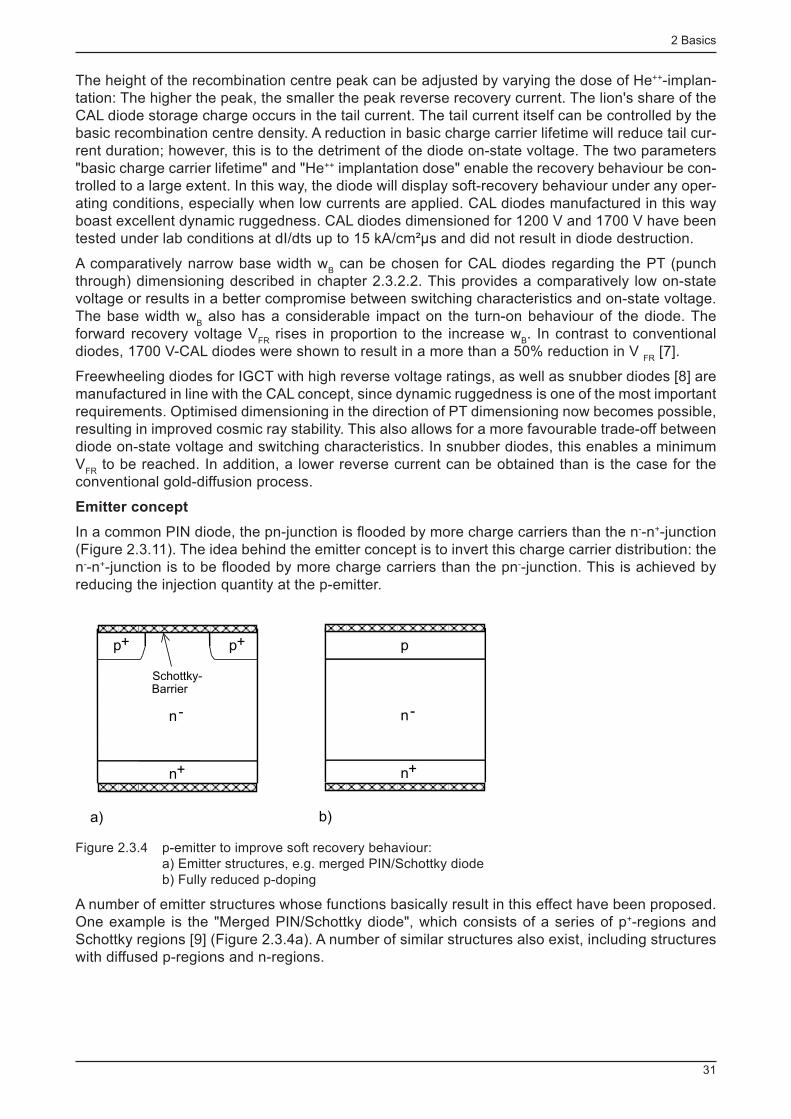
2 Basics
31
The height of the recombination centre peak can be adjusted by varying the dose of He ++ -implan-tation: The higher the peak, the smaller the peak reverse recovery current. The lion's share of the CAL diode storage charge occurs in the tail current. The tail current itself can be controlled by the basic recombination centre density. A reduction in basic charge carrier lifetime will reduce tail cur-rent duration; however, this is to the detriment of the diode on-state voltage. The two parameters "basic charge carrier lifetime" and "He ++ implantation dose" enable the recovery behaviour be con-trolled to a large extent. In this way, the diode will display soft-recovery behaviour under any oper-ating conditions, especially when low currents are applied. CAL diodes manufactured in this way boast excellent dynamic ruggedness. CAL diodes dimensioned for 1200 V and 1700 V have been tested under lab conditions at dI/dts up to 15 kA/cm²µs and did not result in diode destruction.
A comparatively narrow base width w B can be chosen for CAL diodes regarding the PT (punch
through) dimensioning described in chapter 2.3.2.2. This provides a comparatively low on-state voltage or results in a better compromise between switching characteristics and on-state voltage. The base width w
B also has a considerable impact on the turn-on behaviour of the diode. The
forward recovery voltage V FR
rises in proportion to the increase w B . In contrast to conventional
diodes, 1700 V-CAL diodes were shown to result in a more than a 50% reduction in V FR
[7].
Freewheeling diodes for IGCT with high reverse voltage ratings, as well as snubber diodes [8] are manufactured in line with the CAL concept, since dynamic ruggedness is one of the most important requirements. Optimised dimensioning in the direction of PT dimensioning now becomes possible, resulting in improved cosmic ray stability. This also allows for a more favourable trade-off between diode on-state voltage and switching characteristics. In snubber diodes, this enables a minimum V
FR to be reached. In addition, a lower reverse current can be obtained than is the case for the
conventional gold-diffusion process.
Emitter concept
In a common PIN diode, the pn-junction is fl ooded by more charge carriers than the n - -n + -junction (Figure 2.3.11). The idea behind the emitter concept is to invert this charge carrier distribution: the n - -n + -junction is to be fl ooded by more charge carriers than the pn - -junction. This is achieved by reducing the injection quantity at the p-emitter.
n
n-
+
a)
p+ p+
Schottky-Barrier
n
n-
+
b)
p
Figure 2.3.4 p-emitter to improve soft recovery behaviour: a) Emitter structures, e.g. merged PIN/Schottky diode b) Fully reduced p-doping
A number of emitter structures whose functions basically result in this effect have been proposed. One example is the "Merged PIN/Schottky diode", which consists of a series of p + -regions and Schottky regions [9] (Figure 2.3.4a). A number of similar structures also exist, including structures with diffused p-regions and n-regions.
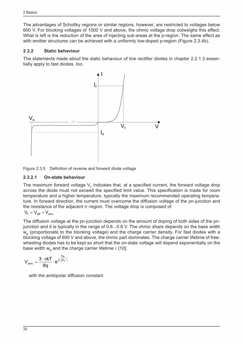
2 Basics
32
The advantages of Schottky regions or similar regions, however, are restricted to voltages below 600 V. For blocking voltages of 1000 V and above, the ohmic voltage drop outweighs this effect. What is left is the reduction of the area of injecting sub-areas at the p-region. The same effect as with emitter structures can be achieved with a uniformly low-doped p-region (Figure 2.3.4b).
2.3.2 Static behaviour
The statements made about the static behaviour of line rectifi er diodes in chapter 2.2.1.3 essen-tially apply to fast diodes, too.
VF
IR
VR
IF
V
I
Figure 2.3.5 Defi nition of reverse and forward diode voltage
2.3.2.1 On-state behaviour
The maximum forward voltage V F indicates that, at a specifi ed current, the forward voltage drop
across the diode must not exceed the specifi ed limit value. This specifi cation is made for room temperature and a higher temperature, typically the maximum recommended operating tempera-ture. In forward direction, the current must overcome the diffusion voltage of the pn-junction and the resistance of the adjacent n - -region. The voltage drop is composed of
ohmdiffF VVV +=
The diffusion voltage at the pn-junction depends on the amount of doping of both sides of the pn-junction and it is typically in the range of 0.6...0.8 V. The ohmic share depends on the base width w
B (proportionate to the blocking voltage) and the charge carrier density. For fast diodes with a
blocking voltage of 600 V and above, the ohmic part dominates. The charge carrier lifetime of free-wheeling diodes has to be kept so short that the on-state voltage will depend exponentially on the base width w
B and the charge carrier lifetime τ [10]:
t××p×
= A
B
D2
w
ohm eq8
kT3V
with the ambipolar diffusion constant
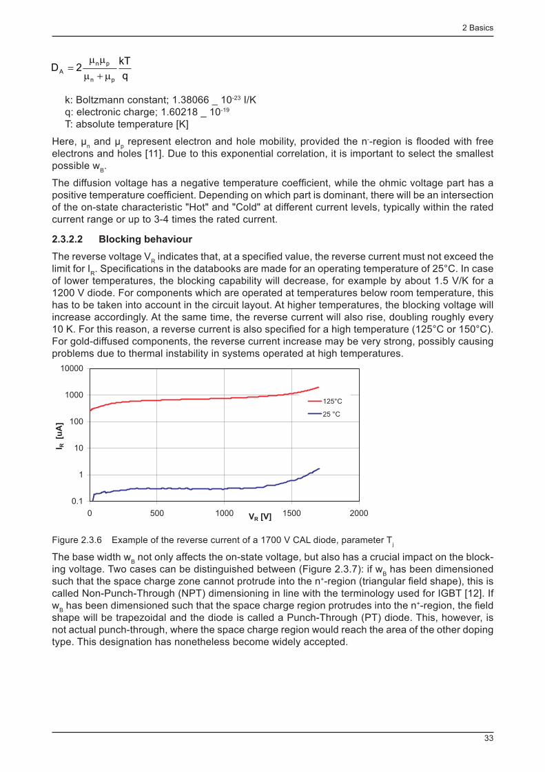
2 Basics
33
q
kT2D
pn
pn
A m+m
mm=
k: Boltzmann constant; 1.38066 _ 10-23 I/K q: electronic charge; 1.60218 _ 10-19
T: absolute temperature [K]
Here, µ n and µ
p represent electron and hole mobility, provided the n - -region is fl ooded with free
electrons and holes [11]. Due to this exponential correlation, it is important to select the smallest possible w
B .
The diffusion voltage has a negative temperature coeffi cient, while the ohmic voltage part has a positive temperature coeffi cient. Depending on which part is dominant, there will be an intersection of the on-state characteristic "Hot" and "Cold" at different current levels, typically within the rated current range or up to 3-4 times the rated current.
2.3.2.2 Blocking behaviour
The reverse voltage V R indicates that, at a specifi ed value, the reverse current must not exceed the
limit for I R . Specifi cations in the databooks are made for an operating temperature of 25°C. In case
of lower temperatures, the blocking capability will decrease, for example by about 1.5 V/K for a 1200 V diode. For components which are operated at temperatures below room temperature, this has to be taken into account in the circuit layout. At higher temperatures, the blocking voltage will increase accordingly. At the same time, the reverse current will also rise, doubling roughly every 10 K. For this reason, a reverse current is also specifi ed for a high temperature (125°C or 150°C). For gold-diffused components, the reverse current increase may be very strong, possibly causing problems due to thermal instability in systems operated at high temperatures.
Reverse Characteristic of a 1700V CAL Diode
0.1
1
10
100
1000
10000
0 500 1000 1500 2000V [V]R
I R[u
A]
125°C
25 °C
Figure 2.3.6 Example of the reverse current of a 1700 V CAL diode, parameter T j
The base width w B not only affects the on-state voltage, but also has a crucial impact on the block-
ing voltage. Two cases can be distinguished between (Figure 2.3.7): if w B has been dimensioned
such that the space charge zone cannot protrude into the n + -region (triangular fi eld shape), this is called Non-Punch-Through (NPT) dimensioning in line with the terminology used for IGBT [12]. If w
B has been dimensioned such that the space charge region protrudes into the n + -region, the fi eld
shape will be trapezoidal and the diode is called a Punch-Through (PT) diode. This, however, is not actual punch-through, where the space charge region would reach the area of the other doping type. This designation has nonetheless become widely accepted.

2 Basics
34
0w
p
n-
n+-E(w)
-E(w)
0wBw
non-punch-through (NPT)-Diode
a)
E0
E1
w*
b)
punch-through (PT)-Diode
p
E0
n+
n-
wB
Figure 2.3.7 Diode dimensioning for triangular (a) and trapezoidal (b) fi eld shape for 0 ≤ w ≤ w
B
For an ideal NPT diode, w B is selected such that, at maximum reverse voltage, the end of the tri-
angular fi eld is located at this point. For optimum doping, the minimum width would then be
6
7
BD6
1
3
2
)NPT(B VC2w =
where C = 1.8·10 -35 cm 6 V -7
The minimum doping needed for PT diodes can be calculated in the same way. In the extreme case, the fi eld would be rectangular, E
1 = E
0 (Figure 2.3.7). This results in
6
7
BD6
1
)Minimum,PT(B VCw ×=
Compared to w B for the NPT diode, the following applies:
)NPT(B)NPT(B3
2
)Minimum,PT(B w63,0w2w ×@=
Although this extreme case cannot be achieved, available technology allows us to come close to this, i.e.:
(NPT)B(PT)B w0,66w ×@
For the charge carrier lifetimes presently in use, the difference in forward voltage for PT dimen-sioning and NPT dimensioning is approximately 0.8 V. For this reason, PT dimensioning is to be given preference if possible.
2.3.3 Dynamic behaviour
2.3.3.1 Turn-on behaviour
When the diode is turned on, it has to overcome the resistance of the low-doped base. The turn-on peak voltage thus increases proportionate to w
B . The turn-on peak voltage becomes especially
critical if a signifi cant base width w B has to be chosen due to a high blocking voltage of more than
1200 V. For this reason, optimum turn-on behaviour is once again achieved with PT diodes.
Freewheeling diodes always contain recombination centres to reduce charge carrier lifetime. Re-combination centres (e.g. gold) causing an increase in base resistance are to be avoided for diodes with a high blocking voltage. Recombination centres generated by platinum diffusion, elec-tron beam radiation or light ions will only slightly increase the turn-on overvoltage in comparison to diodes without recombination centres.
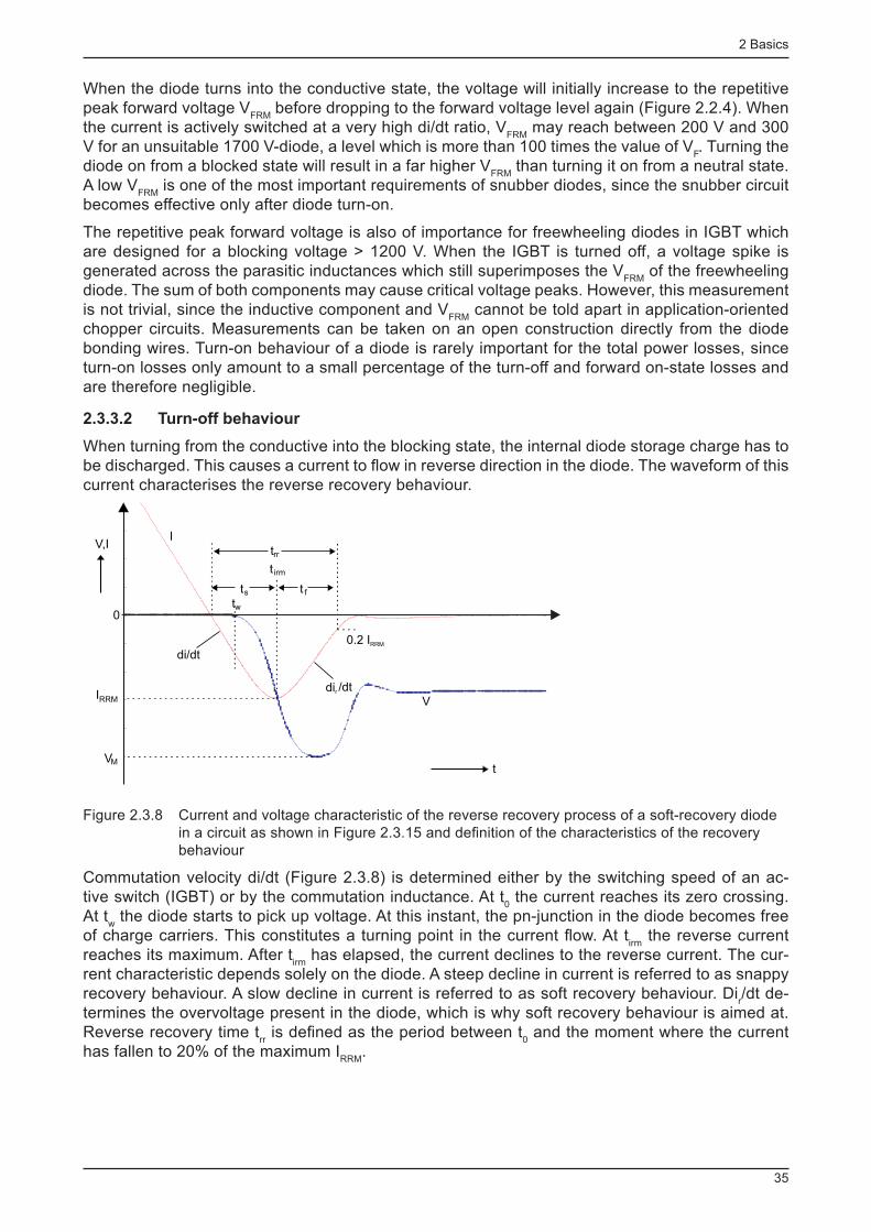
2 Basics
35
When the diode turns into the conductive state, the voltage will initially increase to the repetitive peak forward voltage V
FRM before dropping to the forward voltage level again (Figure 2.2.4). When
the current is actively switched at a very high di/dt ratio, V FRM
may reach between 200 V and 300 V for an unsuitable 1700 V-diode, a level which is more than 100 times the value of V
F . Turning the
diode on from a blocked state will result in a far higher V FRM
than turning it on from a neutral state. A low V
FRM is one of the most important requirements of snubber diodes, since the snubber circuit
becomes effective only after diode turn-on.
The repetitive peak forward voltage is also of importance for freewheeling diodes in IGBT which are designed for a blocking voltage > 1200 V. When the IGBT is turned off, a voltage spike is generated across the parasitic inductances which still superimposes the V
FRM of the freewheeling
diode. The sum of both components may cause critical voltage peaks. However, this measurement is not trivial, since the inductive component and V
FRM cannot be told apart in application-oriented
chopper circuits. Measurements can be taken on an open construction directly from the diode bonding wires. Turn-on behaviour of a diode is rarely important for the total power losses, since turn-on losses only amount to a small percentage of the turn-off and forward on-state losses and are therefore negligible.
2.3.3.2 Turn-off behaviour
When turning from the conductive into the blocking state, the internal diode storage charge has to be discharged. This causes a current to fl ow in reverse direction in the diode. The waveform of this current characterises the reverse recovery behaviour.
VM
IRRM
V,I
0tw
t irm
ts t f
0.2 IRRM
trr
I
V
di/dt
dir /dt
t
Figure 2.3.8 Current and voltage characteristic of the reverse recovery process of a soft-recovery diode in a circuit as shown in Figure 2.3.15 and defi nition of the characteristics of the recovery behaviour
Commutation velocity di/dt (Figure 2.3.8) is determined either by the switching speed of an ac-tive switch (IGBT) or by the commutation inductance. At t
0 the current reaches its zero crossing.
At t w the diode starts to pick up voltage. At this instant, the pn-junction in the diode becomes free
of charge carriers. This constitutes a turning point in the current fl ow. At t irm
the reverse current reaches its maximum. After t
irm has elapsed, the current declines to the reverse current. The cur-
rent characteristic depends solely on the diode. A steep decline in current is referred to as snappy recovery behaviour. A slow decline in current is referred to as soft recovery behaviour. Di
r /dt de-
termines the overvoltage present in the diode, which is why soft recovery behaviour is aimed at. Reverse recovery time t
rr is defi ned as the period between t
0 and the moment where the current
has fallen to 20% of the maximum I RRM
.

2 Basics
36
Soft recovery behaviour and switching overvoltage
As shown in Figure 2.3.8, differentiating between t f and t
s for t
rr helps to defi ne a "soft factor" as a
quantitative characteristic for recovery behaviour:
Soft factor s
f
t
ts =
The soft factor should be greater than 1 in order to minimise switching overvoltages. This defi ni-tion, however, is imprecise. For, according to it, the current characteristic shown in Figure 2.3.9a would be regarded as snappy, whereas the current characteristic as in Figure 2.3.9b would be con-sidered soft. Despite s > 1, there is a steep edge in a part of the reverse current fl ow. A defi nition that refers to the maximum di
f /dt during the fall time t
f would be better. For a soft recovery diode,
di f /dt is within the range of di/dt for t
s .
0.2 IRRM
ts
a) b)
tf ts tf
0.2 IRRM
Figure 2.3.9 Current characteristic for two different possibilities of snappy reverse recovery behaviour
Specifying the recovery behaviour at the nominal operating point only is likewise not suffi ciently meaningful. It varies as a function of different circuit parameters. - Current: Measurements have to be taken at a current fl ow of less than 10% and at 200% of the specifi ed current. This approach gives proper consideration to the fact that small currents are particularly critical for the reverse recovery behaviour.
- Temperature: High temperatures are often more problematic for the recovery behaviour. For cer-tain fast diodes, however, the recovery behaviour will deteriorate at room temperature or below.
- Voltage applied: Higher voltage results in poorer reverse recovery behaviour. - Rate of rise for di/dt: The dependency of di/dt varies greatly in diodes made by different manu-facturers. One type of diode will become "softer" when the di/dt increases, while another will become "snappier".
The best way to charaterise soft recovery behaviour is to measure the turn-off overvoltage under different operating conditions (I
F , T
j , V
CC , di/dt). In a typical application, where the chopper is in a
semiconductor module, the parasitic inductance L sges
is in the range of some 10 nH. This reduces the overvoltage generated. Due to a lack of ideal switches, the voltage applied to the IGBT will drop to a certain degree during the reverse recovery phase. The voltage measured becomes
)t(V
dt
diLV)t(V CE
Rges +×--=- s
where V CE
(t) is the voltage across the IGBT at the given moment in time. In a 100 A soft recovery diodes with moderate rates of rise of up to 1500 A/µs and minimum parasitic inductances, V(t) will very often be smaller than V
CC at any time and no voltage spikes will occur.
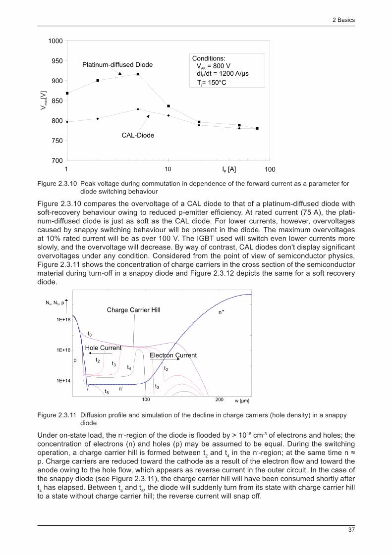
2 Basics
37
700
750
800
850
900
950
1000
1 10 100I [A]F
Conditions:V = 800 VAK
di /dt = 1200 A/µsF
T= 150°Cj
Platinum-diffused Diode
CAL-Diode
V[V
]m
ax
Figure 2.3.10 Peak voltage during commutation in dependence of the forward current as a parameter for diode switching behaviour
Figure 2.3.10 compares the overvoltage of a CAL diode to that of a platinum-diffused diode with soft-recovery behaviour owing to reduced p-emitter effi ciency. At rated current (75 A), the plati-num-diffused diode is just as soft as the CAL diode. For lower currents, however, overvoltages caused by snappy switching behaviour will be present in the diode. The maximum overvoltages at 10% rated current will be as over 100 V. The IGBT used will switch even lower currents more slowly, and the overvoltage will decrease. By way of contrast, CAL diodes don't display signifi cant overvoltages under any condition. Considered from the point of view of semiconductor physics, Figure 2.3.11 shows the concentration of charge carriers in the cross section of the semiconductor material during turn-off in a snappy diode and Figure 2.3.12 depicts the same for a soft recovery diode.
100 200 w [µm]
1E+14
1E+16
1E+18
t2 t3t2
t3
t4
t5
p
n+Charge Carrier Hill
Hole CurrentElectron Current
N , N , pA D
n-
t0
Figure 2.3.11 Diffusion profi le and simulation of the decline in charge carriers (hole density) in a snappy diode
Under on-state load, the n - -region of the diode is fl ooded by > 10 16 cm -3 of electrons and holes; the concentration of electrons (n) and holes (p) may be assumed to be equal. During the switching operation, a charge carrier hill is formed between t
2 and t
4 in the n - -region; at the same time n ≈
p. Charge carriers are reduced toward the cathode as a result of the electron fl ow and toward the anode owing to the hole fl ow, which appears as reverse current in the outer circuit. In the case of the snappy diode (see Figure 2.3.11), the charge carrier hill will have been consumed shortly after t 4 has elapsed. Between t
4 and t
5 , the diode will suddenly turn from its state with charge carrier hill
to a state without charge carrier hill; the reverse current will snap off.

2 Basics
38
The process in a soft-recovery diode is shown in Figure 2.3.12. Throughout the entire process, a charge carrier hill which feeds the reverse current is retained . At t
5 , the diode will already have
picked up the voltage applied. The dynamic behaviour described results in a tail current, as shown in the measurement in Figure 2.3.17.
100 200 w [µm]
1E+14
1E+16
1E+18
t0
t2 t3 t4t4
t5 t6
t5 t6
p
n+
Charge Carrier Hill
Hole CurrentElectron Current
n-
N , N , pA D
Figure 2.3.12 Diffusion profi le and simulated decline in charge carriers (hole density) in a soft recovery diode
Whether soft recovery behaviour will be achieved depends on how successfully this charge carrier reduction is managed. The following measures will result in softer recovery behaviour: - The width w
B in the n - -region is enlarged, NPT dimensioning is used, and a region is also inte-
grated into the diode which cannot be reached by the fi eld at nominal voltage. This, however, will result in a stark increase in on-state voltage or in the V
F /Q
RR relation.
- In order to restrict the increase in w B somewhat, a two-stage n - -region can be used [13] with
increased doping close to the n-n + -junction. Figure 2.3.11 and Figure 2.3.12 demonstrate how a similar effect is achieved by a fl at gradient at the n - -n + -junction. This measure alone, however, will not be enough to achieve soft recovery behaviour.
- Charge carrier distribution is inverted by a low-effi ciency p-emitter ( see "Emitter concept"). - An axial charge carrier lifetime profi le according to the CAL concept, providing for a low charge carrier life at the pn-junction, and a longer charge carrier life at the n - -n + -junction.
To ensure soft recovery behaviour under any conditions, several of these measures normally have to be taken at the same time. That said, the achievements made in this respect must always be assessed with a view to the extent to which a higher on-state voltage or a higher Q
RR is accepted.
Minimum turn-on time
In order to reach the "soft" switching characteristics described above, the charge carriers must be granted suffi cient time to reach the state of quasi-static charge carrier distribution. This is not the case for very short conduction times.
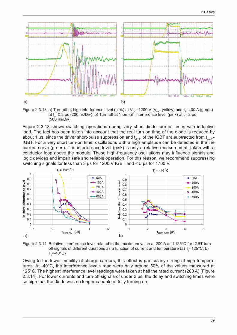
2 Basics
39
Figure 2.3.13 a) Turn-off at high interference level (pink) at V CC
=1200 V (V AK
-yellow) and I F =400 A (green)
at t p =0.8 µs (200 ns/Div); b) Turn-off at "normal" interference level (pink) at t
p =2 µs
(500 ns/Div)
Figure 2.3.13 shows switching operations during very short diode turn-on times with inductive load. The fact has been taken into account that the real turn-on time of the diode is reduced by about 1 µs, since the driver short-pulse suppression and t
d(off) of the IGBT are subtracted from t
p(off) -
IGBT. For a very short turn-on time, oscillations with a high amplitude can be detected in the the current curve (green). The interference level (pink) is only a relative measurement, taken with a conductor loop above the module. These high-frequency oscillations may infl uence signals and logic devices and impair safe and reliable operation. For this reason, we recommend suppressing switching signals for less than 3 µs for 1200 V IGBT and < 5 µs for 1700 V.
T = +125 Cj0
0
0.1
0.2
0.3
0.4
0.5
0.6
0.7
0.8
0.9
1
1 2 3 4 5t [µs]p(off)-IGBT
Re
lati
ve
dis
turb
an
ce
lev
el
50A
100A
200A
400A
600A
0
0.1
0.2
0.3
0.4
0.5
0.6
0.7
0.8
0.9
1
1 2 3 4 5
Re
lati
ve
dis
turb
an
ce
lev
el
a) b)
T = - 40 Cj0
t [µs]p(off)-IGBT
50A
100A
200A
400A
600A
Figure 2.3.14 Relative interference level related to the maximum value at 200 A and 125°C for IGBT turn-off signals of different durations as a function of current and temperature (a) T
j =125°C, b)
T j =-40°C)
Owing to the lower mobility of charge carriers, this effect is particularly strong at high tempera-tures. At -40°C, the interference levels read were only around 50% of the values measured at 125°C. The highest interference level readings were taken at half the rated current (200 A) (Figure 2.3.14). For lower currents and turn-off signals of under 2 µs, the delay and switching times were so high that the diode was no longer capable of fully turning on.
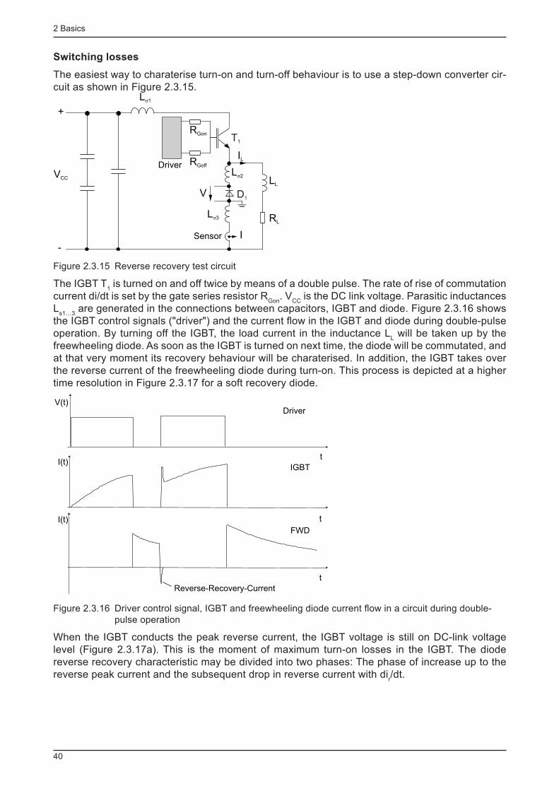
2 Basics
40
Switching losses
The easiest way to charaterise turn-on and turn-off behaviour is to use a step-down converter cir-cuit as shown in Figure 2.3.15.
T1
D1
LL
RGoff
IL
RGon
Ls1
DriverVCC
+
-
Ls2
Ls3
ISensor
V
RL
Figure 2.3.15 Reverse recovery test circuit
The IGBT T 1 is turned on and off twice by means of a double pulse. The rate of rise of commutation
current di/dt is set by the gate series resistor R Gon
. V CC
is the DC link voltage. Parasitic inductances L
s1…3 are generated in the connections between capacitors, IGBT and diode. Figure 2.3.16 shows
the IGBT control signals ("driver") and the current fl ow in the IGBT and diode during double-pulse operation. By turning off the IGBT, the load current in the inductance L
L will be taken up by the
freewheeling diode. As soon as the IGBT is turned on next time, the diode will be commutated, and at that very moment its recovery behaviour will be charaterised. In addition, the IGBT takes over the reverse current of the freewheeling diode during turn-on. This process is depicted at a higher time resolution in Figure 2.3.17 for a soft recovery diode.
I(t)
I(t)IGBT
FWD
t
V(t)Driver
t
t
Reverse-Recovery-Current
Figure 2.3.16 Driver control signal, IGBT and freewheeling diode current fl ow in a circuit during double-pulse operation
When the IGBT conducts the peak reverse current, the IGBT voltage is still on DC-link voltage level (Figure 2.3.17a). This is the moment of maximum turn-on losses in the IGBT. The diode reverse recovery characteristic may be divided into two phases: The phase of increase up to the reverse peak current and the subsequent drop in reverse current with di
r /dt.
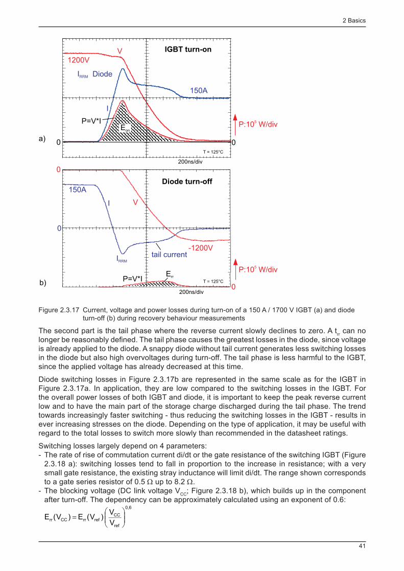
2 Basics
41
Won
Err
IGBT turn-on
Diode turn-off
I
150A
V
1200V
IRRM Diode
P=V*I
P=V*I
0
150A
IRRM
0
0
-1200V
P:10 W/div5
200ns/div
200ns/div
0
0
I V
T = 125°C
T = 125°C
Eon
tail current
b)
a)
P:10 W/div5
Figure 2.3.17 Current, voltage and power losses during turn-on of a 150 A / 1700 V IGBT (a) and diode turn-off (b) during recovery behaviour measurements
The second part is the tail phase where the reverse current slowly declines to zero. A t rr can no
longer be reasonably defi ned. The tail phase causes the greatest losses in the diode, since voltage is already applied to the diode. A snappy diode without tail current generates less switching losses in the diode but also high overvoltages during turn-off. The tail phase is less harmful to the IGBT, since the applied voltage has already decreased at this time.
Diode switching losses in Figure 2.3.17b are represented in the same scale as for the IGBT in Figure 2.3.17a. In application, they are low compared to the switching losses in the IGBT. For the overall power losses of both IGBT and diode, it is important to keep the peak reverse current low and to have the main part of the storage charge discharged during the tail phase. The trend towards increasingly faster switching - thus reducing the switching losses in the IGBT - results in ever increasing stresses on the diode. Depending on the type of application, it may be useful with regard to the total losses to switch more slowly than recommended in the datasheet ratings.
Switching losses largely depend on 4 parameters: - The rate of rise of commutation current di/dt or the gate resistance of the switching IGBT (Figure 2.3.18 a): switching losses tend to fall in proportion to the increase in resistance; with a very small gate resistance, the existing stray inductance will limit di/dt. The range shown corresponds to a gate series resistor of 0.5 Ω up to 8.2 Ω.
- The blocking voltage (DC link voltage V CC
; Figure 2.3.18 b), which builds up in the component after turn-off. The dependency can be approximately calculated using an exponent of 0.6:
6,0
ref
CCrefrrCCrr
V
V)V(E)V(E ÷÷
ø
öççè
æ=
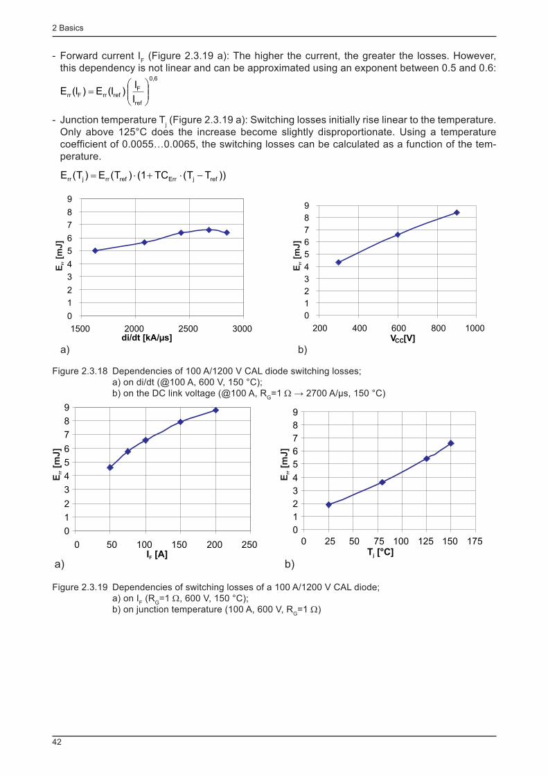
2 Basics
42
- Forward current I F (Figure 2.3.19 a): The higher the current, the greater the losses. However,
this dependency is not linear and can be approximated using an exponent between 0.5 and 0.6:
6,0
ref
FrefrrFrr
I
I)I(E)I(E ÷÷
ø
öççè
æ=
- Junction temperature T j (Figure 2.3.19 a): Switching losses initially rise linear to the temperature.
Only above 125°C does the increase become slightly disproportionate. Using a temperature coeffi cient of 0.0055…0.0065, the switching losses can be calculated as a function of the tem-perature.
))TT(TC(1)T(E)T(E refjErrrefrrjrr -×+×=
0
1
2
3
4
5
6
7
8
9
1500 2000 2500 3000di/dt [kA/µs]
0
1
2
3
4
5
6
7
8
9
200 400 600 800 1000VCC[V]
E[m
J]
rr
E[m
J]
rr
a) b)
Figure 2.3.18 Dependencies of 100 A/1200 V CAL diode switching losses; a) on di/dt (@100 A, 600 V, 150 °C); b) on the DC link voltage (@100 A, R
G =1 Ω → 2700 A/µs, 150 °C)
0
1
2
3
4
5
6
7
8
9
0 50 100 150 200 250I [A]F
0
1
2
3
4
5
6
7
8
9
0 25 50 75 100 125 150 175T [°C]j
E[m
J]
rr
E[m
J]
rr
a) b)
Figure 2.3.19 Dependencies of switching losses of a 100 A/1200 V CAL diode; a) on I
F (R
G =1 Ω, 600 V, 150 °C);
b) on junction temperature (100 A, 600 V, R G =1 Ω)
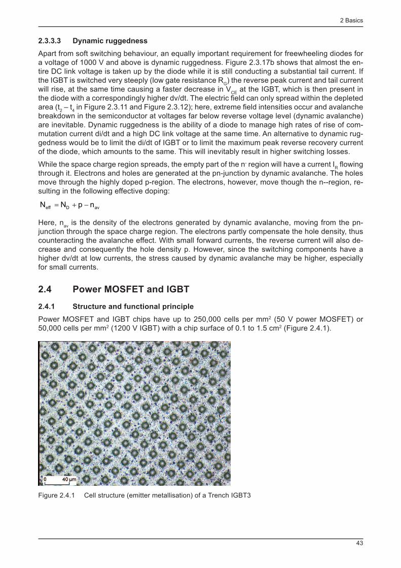
2 Basics
43
2.3.3.3 Dynamic ruggedness
Apart from soft switching behaviour, an equally important requirement for freewheeling diodes for a voltage of 1000 V and above is dynamic ruggedness. Figure 2.3.17b shows that almost the en-tire DC link voltage is taken up by the diode while it is still conducting a substantial tail current. If the IGBT is switched very steeply (low gate resistance R
G ) the reverse peak current and tail current
will rise, at the same time causing a faster decrease in V CE
at the IGBT, which is then present in the diode with a correspondingly higher dv/dt. The electric fi eld can only spread within the depleted area (t
2 – t
4 in Figure 2.3.11 and Figure 2.3.12); here, extreme fi eld intensities occur and avalanche
breakdown in the semiconductor at voltages far below reverse voltage level (dynamic avalanche) are inevitable. Dynamic ruggedness is the ability of a diode to manage high rates of rise of com-mutation current di/dt and a high DC link voltage at the same time. An alternative to dynamic rug-gedness would be to limit the di/dt of IGBT or to limit the maximum peak reverse recovery current of the diode, which amounts to the same. This will inevitably result in higher switching losses.
While the space charge region spreads, the empty part of the n - region will have a current I R fl owing
through it. Electrons and holes are generated at the pn-junction by dynamic avalanche. The holes move through the highly doped p-region. The electrons, however, move though the n--region, re-sulting in the following effective doping:
avDeff npNN -+=
Here, n av
is the density of the electrons generated by dynamic avalanche, moving from the pn-junction through the space charge region. The electrons partly compensate the hole density, thus counteracting the avalanche effect. With small forward currents, the reverse current will also de-crease and consequently the hole density p. However, since the switching components have a higher dv/dt at low currents, the stress caused by dynamic avalanche may be higher, especially for small currents.
2.4 Power MOSFET and IGBT
2.4.1 Structure and functional principle
Power MOSFET and IGBT chips have up to 250,000 cells per mm 2 (50 V power MOSFET) or 50,000 cells per mm 2 (1200 V IGBT) with a chip surface of 0.1 to 1.5 cm 2 (Figure 2.4.1).
Figure 2.4.1 Cell structure (emitter metallisation) of a Trench IGBT3
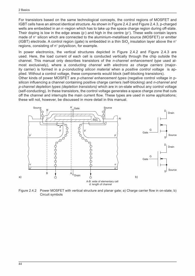
2 Basics
44
For transistors based on the same technological concepts, the control regions of MOSFET and IGBT cells have an almost identical structure. As shown in Figure 2.4.2 and Figure 2.4.3, p-charged wells are embedded in an n - -region which has to take up the space charge region during off-state. Their doping is low in the edge areas (p - ) and high in the centre (p + ). These wells contain layers made of n + silicon which are connected to the aluminium-metallised source (MOSFET) or emitter (IGBT) electrode. A control region (gate) is embedded in a thin SiO
2 insulation layer above the n +
regions, consisting of n + polysilicon, for example.
In power electronics, the vertical structures depicted in Figure 2.4.2 and Figure 2.4.3 are used. Here, the load current of each cell is conducted vertically through the chip outside the channel. This manual only describes transistors of the n-channel enhancement type used al-most exclusively), where a conducting channel with electrons as charge carriers (major-ity carrier) is formed in a p-conducting silicon material when a positive control voltage is ap-plied. Without a control voltage, these components would block (self-blocking transistors). Other kinds of power MOSFET are p-channel enhancement types (negative control voltage in p-silicon infl uencing a channel containing positive charge carriers /self-blocking) and n-channel and
p-channel depletion types (depletion transistors) which are in on-state without any control voltage (self-conducting). In these transistors, the control voltage generates a space charge zone that cuts off the channel and interrupts the main current fl ow. These types are used in some applications; these will not, however, be discussed in more detail in this manual.
SourceB´
A´ Gate Source
AlSiO2
p-
p-
p+
n+
n-
n+
p+
d
n-
n+
B ADrain
A-B: wide of elementary celld: length of channel
a) b)
Source
Source
Drain
Drain
Gate
Gate
D
D
S
S
G
G
-
-
-
-
-
-
-
--
-
-
-
-
-
-
--
-
-
-
-
-
-
-
-
-
-
-
-
-
-
-
Figure 2.4.2 Power MOSFET with vertical structure and planar gate; a) Charge carrier fl ow in on-state; b) Circuit symbols
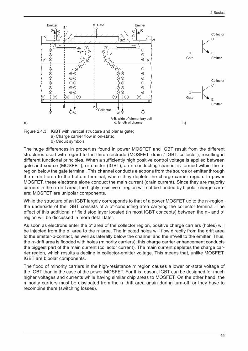
2 Basics
45
-
-
-
-
-
B A
p+
B´A´ Gate Emitter
SiO2
p+
-
-
-
-
-
--
-
-
-
-
--
-
-
-
-
-
-
Al
n+
p-
Emitter
p+
n-
p+
n-
- -Collector
-
-
-
-
p-
d
A-B: wide of elementary celld: length of channel
+
++ +
+
+
2 3 1 1 3 2
C
EG
Gate
Collector
Emitter
a) b)
C
E
G
Gate
Collector
Emitter
Figure 2.4.3 IGBT with vertical structure and planar gate; a) Charge carrier fl ow in on-state; b) Circuit symbols
The huge differences in properties found in power MOSFET and IGBT result from the different structures used with regard to the third electrode (MOSFET: drain / IGBT: collector), resulting in different functional principles. When a suffi ciently high positive control voltage is applied between gate and source (MOSFET), or emitter (IGBT), an n-conducting channel is formed within the p-region below the gate terminal. This channel conducts electrons from the source or emitter through the n - -drift area to the bottom terminal, where they deplete the charge carrier region. In power MOSFET, these electrons alone conduct the main current (drain current). Since they are majority carriers in the n - drift area, the highly resistive n - region will not be fl ooded by bipolar charge carri-ers; MOSFET are unipolar components.
While the structure of an IGBT largely corresponds to that of a power MOSFET up to the n - -region, the underside of the IGBT consists of a p + -conducting area carrying the collector terminal. The effect of this additional n + fi eld stop layer located (in most IGBT concepts) between the n - - and p + region will be discussed in more detail later.
As soon as electrons enter the p + area of the collector region, positive charge carriers (holes) will be injected from the p + area to the n - area. The injected holes will fl ow directly from the drift area to the emitter-p-contact, as well as laterally below the channel and the n + well to the emitter. Thus, the n - -drift area is fl ooded with holes (minority carriers); this charge carrier enhancement conducts the biggest part of the main current (collector current). The main current depletes the charge car-rier region, which results a decline in collector-emitter voltage. This means that, unlike MOSFET, IGBT are bipolar components.
The fl ood of minority carriers in the high-resistance n - region causes a lower on-state voltage of the IGBT than in the case of the power MOSFET. For this reason, IGBT can be designed for much higher voltages and currents while having similar chip areas to MOSFET. On the other hand, the minority carriers must be dissipated from the n - drift area again during turn-off, or they have to recombine there (switching losses).
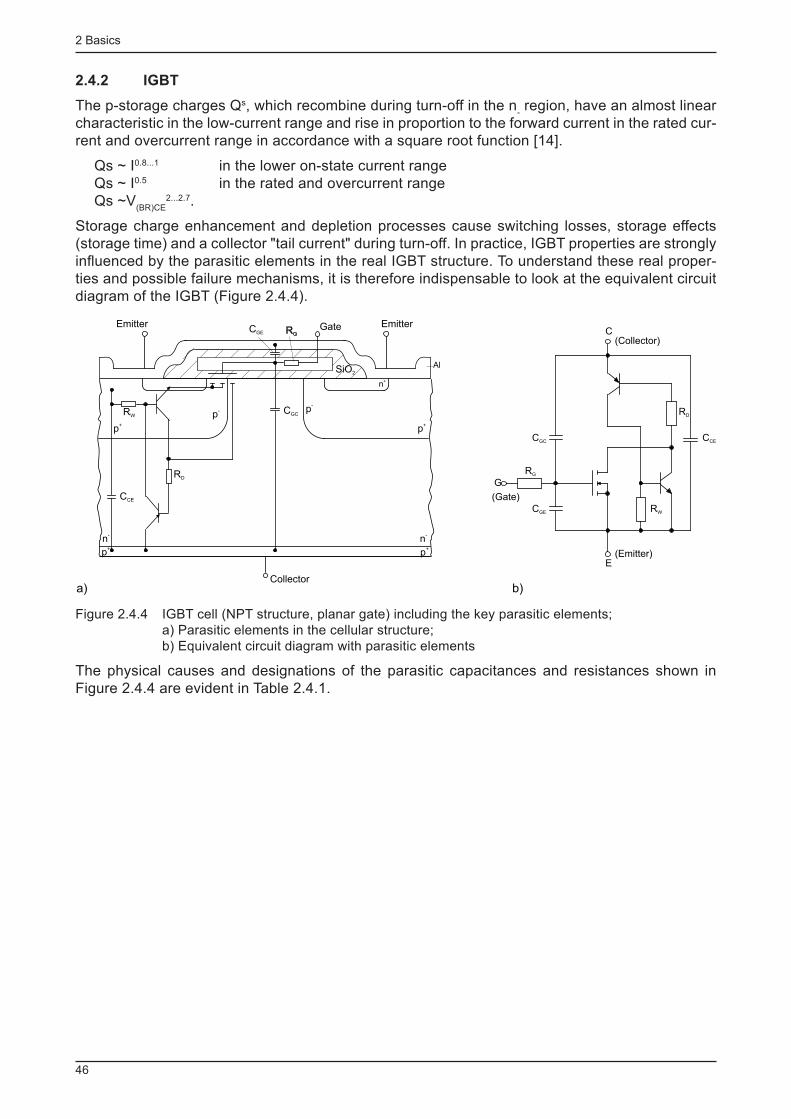
2 Basics
46
2.4.2 IGBT
The p-storage charges Q s , which recombine during turn-off in the n - region, have an almost linear
characteristic in the low-current range and rise in proportion to the forward current in the rated cur-rent and overcurrent range in accordance with a square root function [14].
Qs ~ I 0.8...1 in the lower on-state current range Qs ~ I 0.5 in the rated and overcurrent range Qs ~V
(BR)CE 2...2.7 .
Storage charge enhancement and depletion processes cause switching losses, storage effects (storage time) and a collector "tail current" during turn-off. In practice, IGBT properties are strongly infl uenced by the parasitic elements in the real IGBT structure. To understand these real proper-ties and possible failure mechanisms, it is therefore indispensable to look at the equivalent circuit diagram of the IGBT (Figure 2.4.4).
E(Emitter)
(Collector)C
G
(Gate)
RW
CCECGC
RG
CGE
RD
p+
Emitter
SiO2
p+
Al
n+
p-
Emitter
p+
n-
p+
n-
Collector
p-
Gate
RW
RD
RG
CGC
CGE
CCE
a) b)
Figure 2.4.4 IGBT cell (NPT structure, planar gate) including the key parasitic elements; a) Parasitic elements in the cellular structure; b) Equivalent circuit diagram with parasitic elements
The physical causes and designations of the parasitic capacitances and resistances shown in Figure 2.4.4 are evident in Table 2.4.1.
2 Basics
47
Symbol Designation Physical Description
C GE
Gate-emitter capaci-tance
Overlapping gate and source metallisation; dependent on gate-emitter voltage; independent of collector-emitter volt-age
C CE
Collector-emittercapacitance
Junction capacitance between n - drift area and p-well; de-pendent on cell surface, breakdown voltage and collector-emitter voltage
G GC
Gate-collector-capacitance
Miller capacitance; generated by overlapping of gate and n - -drift area
R G
Internal gate resistance Polysilicon gate resistance; additional series resistors are often needed in modules with several transistor chips to minimise oscillations between chips
R D
Drift resistance Resistance of the n - region (base resistance of the PNPtransistor)
R W
Lateral resistance of the p-well
Base-emitter resistance of the parasitic bipolar NPN transistor
Table 2.4.1 Physical causes and designations of IGBT parasitic elements
Apart from internal capacitances and resistances, the equivalent circuit diagram of the IGBT also shows an "ideal MOSFET", an NPN transistor at the gate side: n + emitter region (emitter) / p + well (base) / n-drift area (collector) with the lateral resistance of the p + well below the emitters as base-emitter resistance R
W and - in the sequence p + -collector area (emitter) / n-drift area (base) / p +
well (collector) - a PNP transistor, which, in combination with the NPN transistor, forms a thyristor circuit. This parasitic thyristor will latch up as soon as the following latch-up condition is met:
( ) 1M pnpnpn =a+a× where ETnpnpnp , g×a=aa
M: multiplication factor; α
npn , α
pnp : current amplifi cation in the individual transistors in the base circuit;
α T : base transport factor;
γ E : emitter effi ciency
This would lead to a loss of IGBT controllability and, consequently, to its destruction. In principle, this can happen during stationary operation (when a critical current density is exceeded, which decreases as the chip temperature rises) or even during turn-off (dynamic latch-up due to the increased hole current compared to stationary on-state operation). Appropriate design measures will reliably prevent latch-up in all modern IGBT types under any permissible static and dynamic operating conditions; latch-up would only happen during turn-off if the rated current density was multiplied in value.
Suitable design measures are, for example, the reduction of the base-emitter resistance R W
of the NPN subtransistor by way of high doping of the p + well directly below the n-emitters and shorten-ing of the n-emitter length to such an extent that the threshold voltage of the base-emitter diode of the NPN transistor cannot be reached under any permissible operating condition. Furthermore, the hole current (NPN transistor base current) is kept at a minimum by setting a low-current am-plifi cation in the PNP transistor. What must be noted here, however, is that a compromise has to be found between switching behaviour and ruggedness, on the one hand, and on-state properties, on the other.
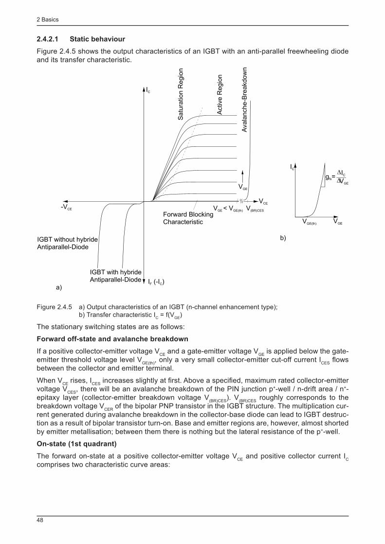
2 Basics
48
2.4.2.1 Static behaviour
Figure 2.4.5 shows the output characteristics of an IGBT with an anti-parallel freewheeling diode and its transfer characteristic.
Forward BlockingCharacteristic
V < VGE GE(th)
I (-I )F C
V(BR)CES-VCE
Avala
nche-B
reakdow
n
Sa
tura
tio
n R
eg
ion
Active R
egio
n
IC
VGE
IGBT with hybrideAntiparallel-Diode
IGBT without hybrideAntiparallel-Diode
IC
VGEVGE(th)
g =fs
IC?VGE
?
VCE
a)
b)
Figure 2.4.5 a) Output characteristics of an IGBT (n-channel enhancement type); b) Transfer characteristic I
C = f(V
GE )
The stationary switching states are as follows:
Forward off-state and avalanche breakdown
If a positive collector-emitter voltage V CE
and a gate-emitter voltage V GE
is applied below the gate-emitter threshold voltage level V
GE(th) , only a very small collector-emitter cut-off current I
CES fl ows
between the collector and emitter terminal.
When V CE
rises, I CES
increases slightly at fi rst. Above a specifi ed, maximum rated collector-emitter voltage V
CES , there will be an avalanche breakdown of the PIN junction p + -well / n-drift area / n + -
epitaxy layer (collector-emitter breakdown voltage V (BR)CES
). V (BR)CES
roughly corresponds to the breakdown voltage V
CER of the bipolar PNP transistor in the IGBT structure. The multiplication cur-
rent generated during avalanche breakdown in the collector-base diode can lead to IGBT destruc-tion as a result of bipolar transistor turn-on. Base and emitter regions are, however, almost shorted by emitter metallisation; between them there is nothing but the lateral resistance of the p + -well.
On-state (1st quadrant)
The forward on-state at a positive collector-emitter voltage V CE
and positive collector current I C
comprises two characteristic curve areas:
2 Basics
49
- Active region
With a gate-emitter voltage V GE
that hardly exceeds the gate-emitter threshold voltage V GE(th)
, a relatively high voltage share will be depleted through the channel owing to current saturation (hori-zontal part of the output characteristics). The collector current I
C is controlled by V
GE .
As a measure for the transfer behaviour as described in Figure 2.4.5b) the forward transconduct-
ance g fs is defi ned as
g fs = ∆I
C /∆V
GE = I
C /( V
GE -V
GE(th) ).
Forward transconductance rises in proportion to the collector current I C and the collector-emitter
voltage V CE
, and falls as the chip temperature increases. In the switching mode that is exclusively permissible for power modules working with several IGBT chips connected in parallel, the active region is only run through during turn-on and turn-off. Stationary module operation in the active region is not permissible, because V
GE(th) falls when the temperature rises, meaning that even small
differences between the individual chips may cause thermal instability.
- Saturation region
The saturation region, which corresponds to ON-state during switching operations (steep part of the output characteristics) has been reached when I
C is solely determined by the outer circuit. The
on-state behaviour is charaterised by the residual voltage V CE(sat)
(collector-emitter saturation volt-age) of the IGBT. Flooding the n - drift area with minority carriers causes the saturation voltage of an IGBT - from a certain reverse voltage level on - to be far lower than the on-state voltage of a comparable MOSFET. In the majority of modern IGBT structures, V
CE(sat) rises in proportion to the
temperature; only for IGBT designed according to the PT concept will V CE(sat)
decline in the rated current range as the temperature increases.
Inverse operation (3rd quadrant)
In inverse operation, the pn-junction of the IGBT at the collector side is poled in reverse direction. The permissible blocking voltage of this PIN diode is no more than a couple of decavolts owing to various design conditions and the shaping of the marginal regions. Today, reverse-blocking IGBT modules are therefore equipped with fast series-connected diodes, whereas reverse-conducting IGBT modules used in standard applications are equipped with fast, anti-parallel diodes (inverse diodes). Thus, the on-state features of IGBT modules in inverse operation exclusively result from the properties of these hybrid inverse diodes. Chapter 2.4.2.3 contains information on the latest developments in reverse-conducting IGBT chips.
2.4.2.2 Switching behaviour
The switching behaviour of IGBT power modules is determined by their structural, internal capaci-tances and the internal and outer resistances. Contrary to the ideal of powerless voltage control via the MOS-gate, frequency-dependent control power is required owing to the recharge currents of the internal capacitances which are needed for switching.
Furthermore, the commutation processes are affected by the parasitic connection inductances present in the components and connections and generated by connecting transistor chips in power modules; they induce transient overvoltages and may cause oscillations due to the circuit and transistor capacitances, cf. chapter 5.
The switching behaviour of IGBT can be described as resulting from the transistor's internal ca-pacitances and resistances:
When the IGBT is turned off, C GC
is low and approximately equal to C CE
. During on-state, C GC
will increase rapidly as soon as the gate-emitter voltage has exceeded the collector-emitter voltage; this rapid increase is due to inversion in the enhancement layer below the gate regions.
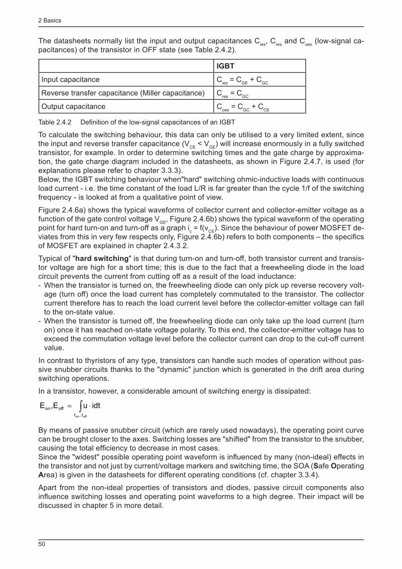
2 Basics
50
The datasheets normally list the input and output capacitances C ies
, C res
and C oes
(low-signal ca-pacitances) of the transistor in OFF state (see Table 2.4.2).
IGBT
Input capacitance C ies
= C GE
+ C GC
Reverse transfer capacitance (Miller capacitance) C res
= C GC
Output capacitance C oes
= C GC
+ C CE
Table 2.4.2 Defi nition of the low-signal capacitances of an IGBT
To calculate the switching behaviour, this data can only be utilised to a very limited extent, since the input and reverse transfer capacitance (V
CE < V
GE ) will increase enormously in a fully switched
transistor, for example. In order to determine switching times and the gate charge by approxima-tion, the gate charge diagram included in the datasheets, as shown in Figure 2.4.7, is used (for explanations please refer to chapter 3.3.3).Below, the IGBT switching behaviour when"hard" switching ohmic-inductive loads with continuous load current - i.e. the time constant of the load L/R is far greater than the cycle 1/f of the switching frequency - is looked at from a qualitative point of view.
Figure 2.4.6a) shows the typical waveforms of collector current and collector-emitter voltage as a function of the gate control voltage V
GE , Figure 2.4.6b) shows the typical waveform of the operating
point for hard turn-on and turn-off as a graph i c = f(v
CE ). Since the behaviour of power MOSFET de-
viates from this in very few respects only, Figure 2.4.6b) refers to both components – the specifi cs of MOSFET are explained in chapter 2.4.3.2.
Typical of " hard switching " is that during turn-on and turn-off, both transistor current and transis-tor voltage are high for a short time; this is due to the fact that a freewheeling diode in the load circuit prevents the current from cutting off as a result of the load inductance: - When the transistor is turned on, the freewheeling diode can only pick up reverse recovery volt-age (turn off) once the load current has completely commutated to the transistor. The collector current therefore has to reach the load current level before the collector-emitter voltage can fall to the on-state value.
- When the transistor is turned off, the freewheeling diode can only take up the load current (turn on) once it has reached on-state voltage polarity. To this end, the collector-emitter voltage has to exceed the commutation voltage level before the collector current can drop to the cut-off current value.
In contrast to thyristors of any type, transistors can handle such modes of operation without pas-sive snubber circuits thanks to the "dynamic" junction which is generated in the drift area during switching operations.
In a transistor, however, a considerable amount of switching energy is dissipated:
ò ×=
offon t,t
offon idtuE,E
By means of passive snubber circuit (which are rarely used nowadays), the operating point curve can be brought closer to the axes. Switching losses are "shifted" from the transistor to the snubber, causing the total effi ciency to decrease in most cases. Since the "widest" possible operating point waveform is infl uenced by many (non-ideal) effects in the transistor and not just by current/voltage markers and switching time, the SOA ( S afe O perating A rea) is given in the datasheets for different operating conditions (cf. chapter 3.3.4).
Apart from the non-ideal properties of transistors and diodes, passive circuit components also infl uence switching losses and operating point waveforms to a high degree. Their impact will be discussed in chapter 5 in more detail.
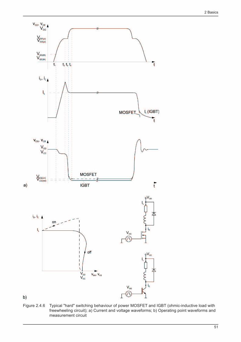
2 Basics
51
Figure 2.4.6 Typical "hard" switching behaviour of power MOSFET and IGBT (ohmic-inductive load with freewheeling circuit); a) Current and voltage waveforms; b) Operating point waveforms and measurement circuit
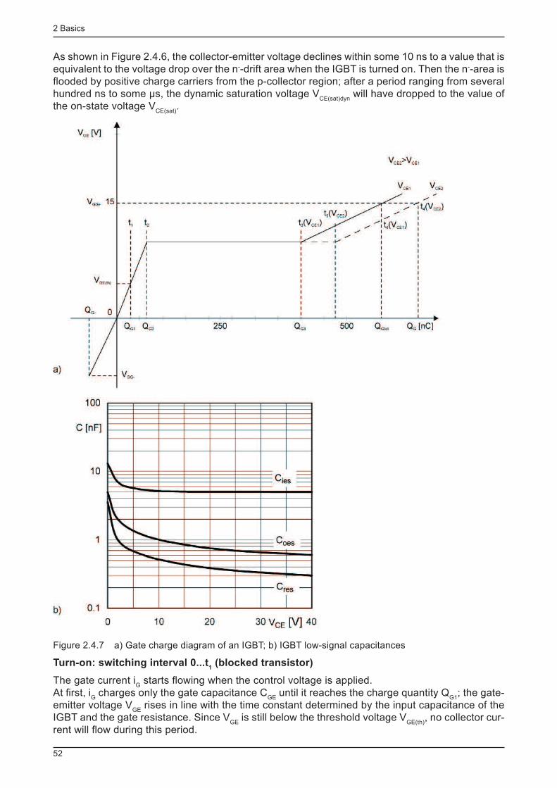
2 Basics
52
As shown in Figure 2.4.6, the collector-emitter voltage declines within some 10 ns to a value that is equivalent to the voltage drop over the n - -drift area when the IGBT is turned on. Then the n - -area is fl ooded by positive charge carriers from the p-collector region; after a period ranging from several hundred ns to some μs, the dynamic saturation voltage V
CE(sat)dyn will have dropped to the value of
the on-state voltage V CE(sat)
.
Figure 2.4.7 a) Gate charge diagram of an IGBT; b) IGBT low-signal capacitances
Turn-on: switching interval 0...t 1 (blocked transistor)
The gate current i G starts fl owing when the control voltage is applied.
At fi rst, i G charges only the gate capacitance C
GE until it reaches the charge quantity Q
G1 ; the gate-
emitter voltage V GE
rises in line with the time constant determined by the input capacitance of the IGBT and the gate resistance. Since V
GE is still below the threshold voltage V
GE(th) , no collector cur-
rent will fl ow during this period.
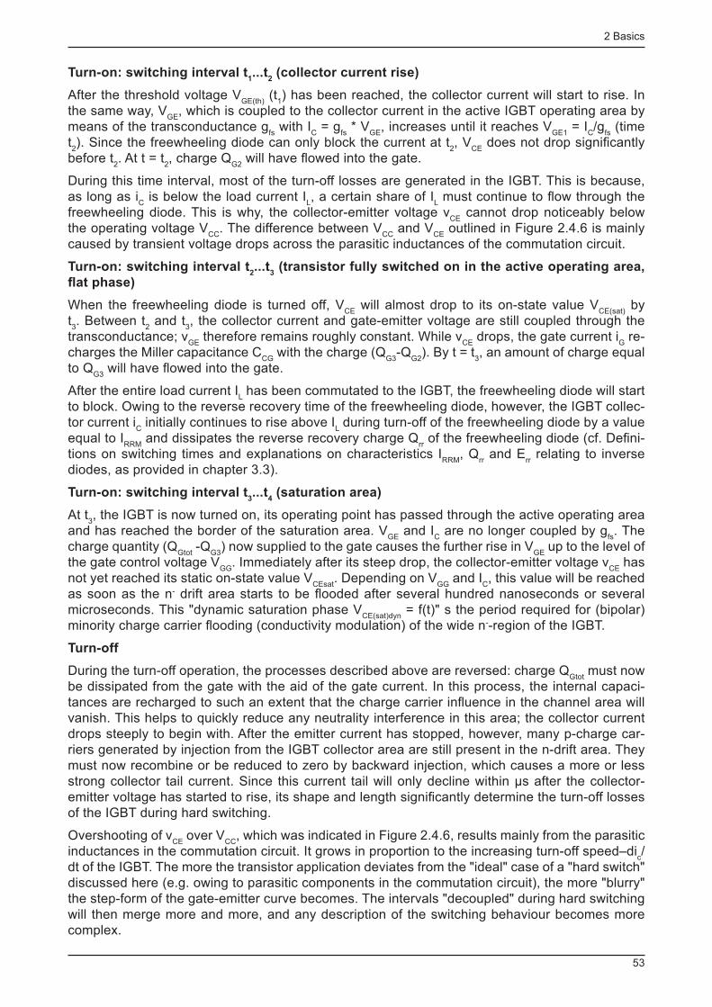
2 Basics
53
Turn-on: switching interval t 1 ...t
2 (collector current rise)
After the threshold voltage V GE(th)
(t 1 ) has been reached, the collector current will start to rise. In
the same way, V GE
, which is coupled to the collector current in the active IGBT operating area by means of the transconductance g
fs with I
C = g
fs * V
GE , increases until it reaches V
GE1 = I
C /g
fs (time
t 2 ). Since the freewheeling diode can only block the current at t
2 , V
CE does not drop signifi cantly
before t 2 . At t = t
2 , charge Q
G2 will have fl owed into the gate.
During this time interval, most of the turn-off losses are generated in the IGBT. This is because, as long as i
C is below the load current I
L , a certain share of I
L must continue to fl ow through the
freewheeling diode. This is why, the collector-emitter voltage v CE
cannot drop noticeably below the operating voltage V
CC . The difference between V
CC and V
CE outlined in Figure 2.4.6 is mainly
caused by transient voltage drops across the parasitic inductances of the commutation circuit.
Turn-on: switching interval t 2 ...t
3 (transistor fully switched on in the active operating area,
fl at phase)
When the freewheeling diode is turned off, V CE
will almost drop to its on-state value V CE(sat)
by t 3 . Between t
2 and t
3 , the collector current and gate-emitter voltage are still coupled through the
transconductance; v GE
therefore remains roughly constant. While v CE
drops, the gate current i G re-
charges the Miller capacitance C CG
with the charge (Q G3
-Q G2
). By t = t 3 , an amount of charge equal
to Q G3
will have fl owed into the gate.
After the entire load current I L has been commutated to the IGBT, the freewheeling diode will start
to block. Owing to the reverse recovery time of the freewheeling diode, however, the IGBT collec-tor current i
C initially continues to rise above I
L during turn-off of the freewheeling diode by a value
equal to I RRM
and dissipates the reverse recovery charge Q rr of the freewheeling diode (cf. Defi ni-
tions on switching times and explanations on characteristics I RRM
, Q rr and E
rr relating to inverse
diodes, as provided in chapter 3.3).
Turn-on: switching interval t 3 ...t
4 (saturation area)
At t 3 , the IGBT is now turned on, its operating point has passed through the active operating area
and has reached the border of the saturation area. V GE
and I C are no longer coupled by g
fs . The
charge quantity (Q Gtot
-Q G3
) now supplied to the gate causes the further rise in V GE
up to the level of the gate control voltage V
GG . Immediately after its steep drop, the collector-emitter voltage v
CE has
not yet reached its static on-state value V CEsat
. Depending on V GG
and I C , this value will be reached
as soon as the n - drift area starts to be fl ooded after several hundred nanoseconds or several microseconds. This "dynamic saturation phase V
CE(sat)dyn = f(t)" s the period required for (bipolar)
minority charge carrier fl ooding (conductivity modulation) of the wide n - -region of the IGBT.
Turn-off
During the turn-off operation, the processes described above are reversed: charge Q Gtot
must now be dissipated from the gate with the aid of the gate current. In this process, the internal capaci-tances are recharged to such an extent that the charge carrier infl uence in the channel area will vanish. This helps to quickly reduce any neutrality interference in this area; the collector current drops steeply to begin with. After the emitter current has stopped, however, many p-charge car-riers generated by injection from the IGBT collector area are still present in the n-drift area. They must now recombine or be reduced to zero by backward injection, which causes a more or less strong collector tail current. Since this current tail will only decline within µs after the collector-emitter voltage has started to rise, its shape and length signifi cantly determine the turn-off losses of the IGBT during hard switching.
Overshooting of v CE
over V CC
, which was indicated in Figure 2.4.6, results mainly from the parasitic inductances in the commutation circuit. It grows in proportion to the increasing turn-off speed–di
c /
dt of the IGBT. The more the transistor application deviates from the "ideal" case of a "hard switch" discussed here (e.g. owing to parasitic components in the commutation circuit), the more "blurry" the step-form of the gate-emitter curve becomes. The intervals "decoupled" during hard switching will then merge more and more, and any description of the switching behaviour becomes more complex.
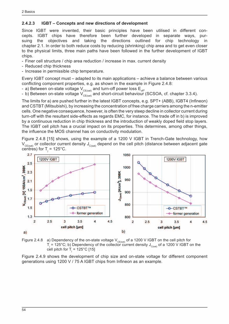
2 Basics
54
2.4.2.3 IGBT – Concepts and new directions of development
Since IGBT were invented, their basic principles have been utilised in different con-cepts. IGBT chips have therefore been further developed in separate ways, pur-suing the objectives and taking the directions outlined for chip technology in chapter 2.1. In order to both reduce costs by reducing (shrinking) chip area and to get even closer to the physical limits, three main paths have been followed in the further development of IGBT chips. - Finer cell structure / chip area reduction / increase in max. current density - Reduced chip thickness - Increase in permissible chip temperature.
Every IGBT concept must – adapted to its main applications – achieve a balance between various confl icting component properties, e.g. as shown in the example in Figure 2.4.8: - a) Between on-state voltage V
CE(sat) and turn-off power loss E
off ,
- b) Between on-state voltage V CE(sat)
and short-circuit behaviour (SCSOA, cf. chapter 3.3.4).
The limits for a) are pushed further in the latest IGBT concepts, e.g. SPT+ (ABB), IGBT4 (Infi neon) and CSTBT (Mitsubishi), by increasing the concentration of free charge carriers among the n-emitter cells. One negative consequence, however, is often the very steep decline in collector current during turn-off with the resultant side-effects as regards EMC, for instance. The trade off in b) is improved by a continuous reduction in chip thickness and the introduction of weakly doped fi eld stop layers. The IGBT cell pitch has a crucial impact on its properties. This determines, among other things, the infl uence the MOS channel has on conductivity modulation.
Figure 2.4.8 [15] shows, using the example of a 1200 V IGBT in Trench-Gate technology, how V
CE(sat) or collector current density J
C(sat) depend on the cell pitch (distance between adjacent gate
centres) for T j = 125°C.
Figure 2.4.8 a) Dependency of the on-state voltage V CE(sat)
of a 1200 V IGBT on the cell pitch for T
j = 125°C; b) Dependency of the collector current density J
C(sat) of a 1200 V IGBT on the
cell pitch for T j = 125°C [15]
Figure 2.4.9 shows the development of chip size and on-state voltage for different component generations using 1200 V / 75 A IGBT chips from Infi neon as an example.

2 Basics
55
Figure 2.4.9 Development of chip size and on-state voltage of 1200 V / 75 A IGBT chips from Infi neon [16]
To enable system costs (cooling, chip area) to be reduced, a crucial development target is to in-crease the permissible chip temperature. This was achieved by Infi neon, for example, for IGBT up to 1700 V in the IGBT4 chip generation, raising the temperature from 150°C to 175°C; 200°C is planned for future IGBT generations. An increase in the IGBT operating temperature, however, means that the freewheeling diode (inverse diode), too, has to be suitable for this temperature; this is increasing the requirements that IGBT module packaging has to fulfi l; cf. chapter 2.5.
The pictures below illustrate the most important IGBT concepts, which shall be briefl y described below. Detailed explanations on the physical correlations are provided in [17], et al.
n- - Basis (substrate)n- - Basis (substrate)
Collector
GateEmitter
IGBT3
Trench + Field stop
n+ - Field stop
Advantage
Implanted back-emitter,
better adjustable
Performance
Lower switching losses
Higher switching
robustness
Advantage
Optimised charge
carrier Modulation
Performance
Lower switching losses
Improved “softness”
Robustness like NPT
n- - Basis (epi)
Collector
n+
p+ - Emitter (substrate)
GateEmitter
Punch Through
n- - Basis (substrate)
Collector
GateEmitter
IGBT (1/2)
Punch Through
Collector
GateEmitter
IGBT4
Trench + Field stop
n+ - Field stop
Advantage
Implanted back-emitter
Implanted field stop
enables thinner base
region
Performance
Lower VCE(sat)
Lower switching losses
Robustness like NPT
- buffer (epi)
Figure 2.4.10 IGBT concepts, basic properties and off-state fi eld intensity characteristics (acc. to [18])

2 Basics
56
PT concept
The fi rst " P unch T hrough" (PT) concept, which is still used today as a result of continuous develop-ments, uses a p + -substrate as a base material , n + and n - region being applied by means of epitaxy. Today, PT-IGBT can also have a trench-gate structure, as shown in Figure 2.4.10. In forward off-state, the space charge region comprises the entire n - -region. In order to keep the epitaxy layer as thin as possible even for high blocking voltages, the fi eld at the end of the n - drift area is reduced by a highly doped n + buffer region.
PT-IGBT have a high emitter effi ciency for holes in the p + layer drifting into the n - drift area, be-cause the substrate is relatively thick and highly doped. The PNP current gain has to be reduced via the base transport factor (n - drift area, n + buffer), which is achieved by reducing the charge carrier lifetime in the n + layer by increasing the recombination centres (e.g. gold doping or electron beam radiation). The hole current amounts to 40...45% of the total current.
NPT concept
The basis of " N on P unch T hrough" (NPT) IGBT, which was soon introduced by numerous manu-facturers, is a thin, weakly doped n - wafer; the collector-side p + zone is created by way of back implantation. Here, the n - drift area is so wide that in forward off-state, the electric fi eld is fully de-pleted in the n - drift area up to the maximum permissible off-state voltage and cannot – in contrast to the PT concept – spread over the entire n - region.
NPT-IGBT have a very thin collector-side p + emitter region, which results in a low emitter effi ciency (γ
E = 0.5) of the PNP subtransistor - it is not necessary to lower the base transport factor by reduc-
ing charge carrier life time. The hole current amounts to 20...25% of the total current. In contrast to PT-IGBT, the saturation voltage of NPT-IGBT has a positive temperature coeffi cient, improving both the current symmetry between the cells in single chip and between chips connected in paral-lel. Switching times for hard switching are comparatively shorter and less dependent on tempera-ture; overcurrents can be better cut off as a result of improved internal current limiting. On the date of creation of this paper, SEMIKRON was using the IGBT2 generation in older NPT-IGBT product series.
SPT- and SPT+ concept
The " S oft P unch T hrough" (SPT)-IGBT by ABB is a further development of the NPT concept. Here, too, the base material is a thin, weakly doped n - wafer; the p + region at the collector is generated by back implantation. Here, an additional p + region has been implanted as a fi eld stop layer above the collector n + region. This reduces the thickness of the drift area – like the highly doped n + buffer layer in the PT-concept – by diminishing the electric fi eld at the end of the n - drift area in front of the collector region. Since this layer needn't curb the high emitter effi ciency as is the case in the PT-IGBT, but has to reduce the fi eld intensity only, it is less highly doped than the n + buffer of the PT-IGBT.
With the same forward off-state voltage, the thickness w B of the n - drift area can be signifi cantly
reduced in comparison to an NPT-IGBT; this also considerably cuts the on-state voltage (~ w B ) of
the drift area. The positive temperature coeffi cient of the on-state voltage and the high component ruggedness are maintained. Figure 2.4.11 shows a cross-sectional view of an SPT-IGBT as well as a comparison of PT-NPT and SPT-IGBT chip thickness.
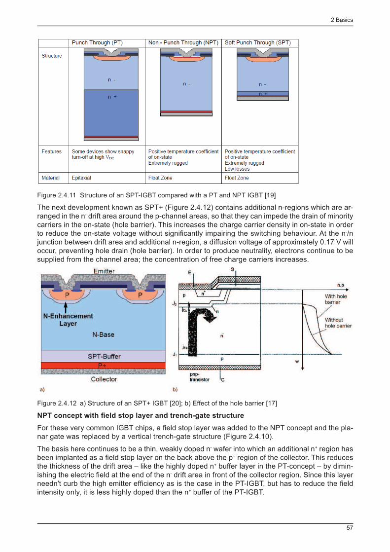
2 Basics
57
Figure 2.4.11 Structure of an SPT-IGBT compared with a PT and NPT IGBT [19]
The next development known as SPT+ (Figure 2.4.12) contains additional n-regions which are ar-ranged in the n - drift area around the p-channel areas, so that they can impede the drain of minority carriers in the on-state (hole barrier). This increases the charge carrier density in on-state in order to reduce the on-state voltage without signifi cantly impairing the switching behaviour. At the n - /n junction between drift area and additional n-region, a diffusion voltage of approximately 0.17 V will occur, preventing hole drain (hole barrier). In order to produce neutrality, electrons continue to be supplied from the channel area; the concentration of free charge carriers increases.
Figure 2.4.12 a) Structure of an SPT+ IGBT [20]; b) Effect of the hole barrier [17]
NPT concept with fi eld stop layer and trench-gate structure
For these very common IGBT chips, a fi eld stop layer was added to the NPT concept and the pla-nar gate was replaced by a vertical trench-gate structure (Figure 2.4.10).
The basis here continues to be a thin, weakly doped n - wafer into which an additional n + region has been implanted as a fi eld stop layer on the back above the p + region of the collector. This reduces the thickness of the drift area – like the highly doped n + buffer layer in the PT-concept – by dimin-ishing the electric fi eld at the end of the n - drift area in front of the collector region. Since this layer needn't curb the high emitter effi ciency as is the case in the PT-IGBT, but has to reduce the fi eld intensity only, it is less highly doped than the n + buffer of the PT-IGBT.
2 Basics
58
With the same forward off-state voltage, the thickness w B of the n - drift area can be signifi cantly
reduced in comparison to an NPT-IGBT; this also considerably cuts the on-state voltage (~ w B ) of
the drift area. The positive temperature coeffi cient of the on-state voltage and the high component ruggedness are maintained. During turn-off, the tail current is initially somewhat higher than for an IGBT without fi eld stop layer, but then it drops faster.
The vertical gate arrangement in the shape of a trench inside every IGBT cell allows for a vertical channel track in the p-well. Since the active silicon area is enlarged, better control of the channel cross-section is possible and thus a lower channel resistance can be obtained. For a given silicon area, the cell area can be reduced even further. This is why higher current densities, lower forward losses, a higher latch-up strength, lower switching losses and higher breakdown voltages can be obtained than in IGBT with planar gate structures.
In the IGBT4 generation from Infi neon, the latest generation when this manual was written, cell pitch (i.e. the distance between the gates of neighbouring cells) was further reduced compared to its predecessor generation IGBT3, meaning that the cells were shrunk in size. Cell optimisation and chip thickness reduction has helped to improve the static and dynamic properties. However, smaller chips also mean a higher thermal contact resistance R
th(j-c) or R
th(j-s) . The performance in-
crease achieved in comparison to the IGBT3 therefore largely results from the higher permissible chip temperature of 175°C as compared with 150°C for IGBT3. Chips are now available with dif-ferent settings between static and dynamic properties for different requirements: - IGBT4 T4: particularly short switching times for modules with rated currents between 10 A and 300 A
- IGBT4 E4: low forward and switching losses for modules from 150 A to 1000 A - IGBT4 P4: "soft" switching behaviour and particularly low forward losses for high-current IGBT modules above rated currents of 900 A.
At the time of publication, SEMIKRON was using IGBT3 chips in older product series and IGBT4 chips T4 and E4 in new product series.
CSTBT concept
A combination of the hole barrier above the drift zone and the trench-gate structure can be found in the C arrier S tored T rench Gate B ipolar T ransistor (CSTBT) from Mitsubishi (Figure 2.4.13). In these IGBT, which were formerly also known as I njection E nhanced G ated T ransistors (IEGT), the charge carrier injection among the n-emitters is increased by a "hole barrier", as described for the SPT + concept. The additional n-doped region is inside the trench-gate structure below the p-base areas. Positive charge carriers are enhanced below the hole barriers, which results in an effective resupply of electrons from the channel and thus a local increase in free charge carrier concentra-tion.
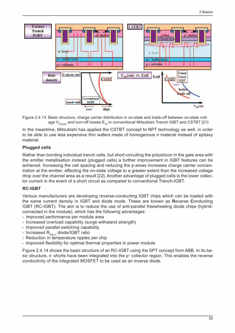
2 Basics
59
Figure 2.4.13 Basic structure, charge carrier distribution in on-state and trade-off between on-state volt-age V
CE(sat) and turn-off losses E
off in conventional Mitsubishi Trench IGBT and CSTBT [21]
In the meantime, Mitsubishi has applied the CSTBT concept to NPT technology as well, in order to be able to use less expensive thin wafers made of homogenous n material instead of epitaxy material.
Plugged cells
Rather than bonding individual trench cells, but short-circuiting the polysilicon in the gate area with the emitter metallisation instead (plugged cells) a further improvement in IGBT features can be achieved. Increasing the cell spacing and reducing the p-areas increases charge carrier concen-tration at the emitter, affecting the on-state voltage to a greater extent than the increased voltage drop over the channel area as a result [22]. Another advantage of plugged cells is the lower collec-tor current in the event of a short circuit as compared to conventional Trench-IGBT.
RC-IGBT
Various manufacturers are developing reverse-conducting IGBT chips which can be loaded with the same current density in IGBT and diode mode. These are known as R everse C onducting IGBT (RC-IGBT). The aim is to reduce the use of anti-parallel freewheeling diode chips (hybrid-connected in the module), which has the following advantages: - Improved performance per module area - Increased overload capability (surge withstand strength) - Improved parallel switching capability - Increased R
th(j-c) diode/IGBT ratio
- Reduction in temperature ripples per chip - Improved fl exibility for optimal thermal properties in power module
Figure 2.4.14 shows the basic structure of an RC-IGBT using the SPT concept from ABB. In its ba-sic structure, n - shorts have been integrated into the p + collector region. This enables the reverse conductivity of the integrated MOSFET to be used as an inverse diode.
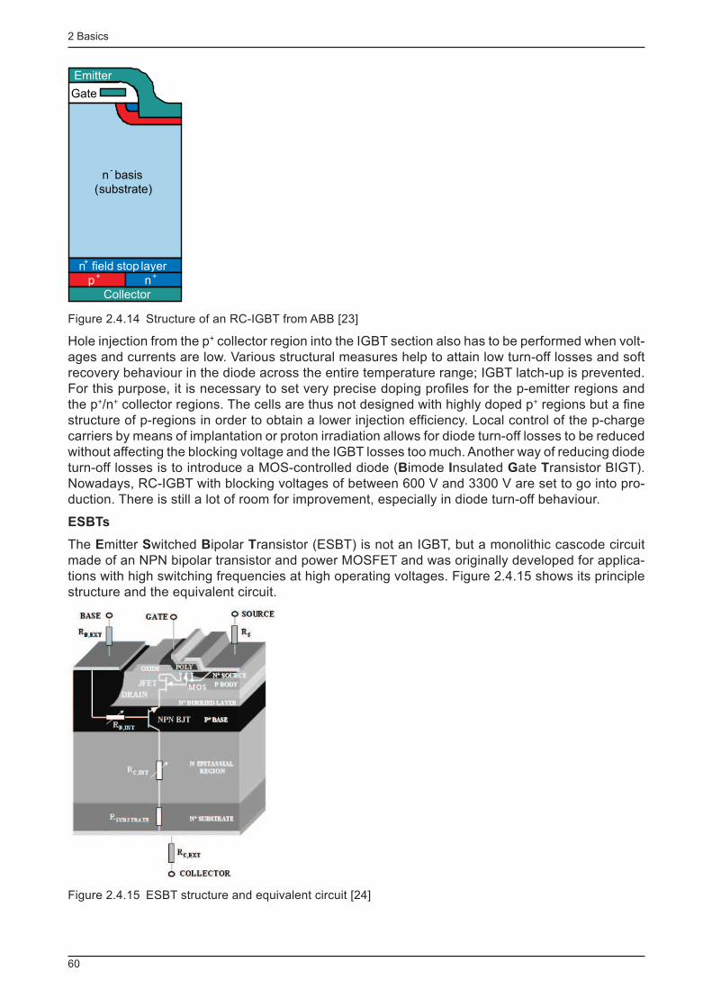
2 Basics
60
Gate
n-basis
(substrate)
Emitter
n+ field stop layer
p+
Collector
n+
Figure 2.4.14 Structure of an RC-IGBT from ABB [23]
Hole injection from the p + collector region into the IGBT section also has to be performed when volt-ages and currents are low. Various structural measures help to attain low turn-off losses and soft recovery behaviour in the diode across the entire temperature range; IGBT latch-up is prevented. For this purpose, it is necessary to set very precise doping profi les for the p-emitter regions and the p + /n + collector regions. The cells are thus not designed with highly doped p + regions but a fi ne structure of p-regions in order to obtain a lower injection effi ciency. Local control of the p-charge carriers by means of implantation or proton irradiation allows for diode turn-off losses to be reduced without affecting the blocking voltage and the IGBT losses too much. Another way of reducing diode turn-off losses is to introduce a MOS-controlled diode ( B imode I nsulated G ate T ransistor BIGT).Nowadays, RC-IGBT with blocking voltages of between 600 V and 3300 V are set to go into pro-duction. There is still a lot of room for improvement, especially in diode turn-off behaviour.
ESBTs
The E mitter S witched B ipolar T ransistor (ESBT) is not an IGBT, but a monolithic cascode circuit made of an NPN bipolar transistor and power MOSFET and was originally developed for applica-tions with high switching frequencies at high operating voltages. Figure 2.4.15 shows its principle structure and the equivalent circuit.
Figure 2.4.15 ESBT structure and equivalent circuit [24]

2 Basics
61
Circuits based on a cascode comprising a low-volt MOSFET and high-volt bipolar transistor were already being employed in discrete components or hybrid-integrated layouts in the eighties. The MOSFET is located in the emitter circuit of the bipolar transistor (series connection). In ON-state, the bipolar transistor and MOSFET are fully controlled. The ESBT on-state voltage is the sum of the on-state voltages of the high-volt bipolar transistor and low-volt MOSFET.
The ESBT is controlled by the MOSFET gate, the base of the bipolar transistor is permanently con-nected to a voltage source via resistors. During turn-off, the MOSFET opens the emitter circuit of the bipolar transistor and the collector current fl ows through the base to the driver voltage source until all charge carriers in the bipolar transistor have been discharged or recombined and the col-lector current is extinguished. Since the emitter is disconnected by the MOSFET during turn-off, there is no risk of a second breakdown of the bipolar structure; the base current extends the limits of the RBSOA (cf. chapter 3.3.4) as compared to regular switching, and component turn-off is pos-sible up to the limiting value V
CB0 of the collector-base diode. MOSFET gate control enables the
driver output to be comparatively low.
2.4.3 Power MOSFET
While the drain-source ON-resistance R DS(on)
of low-voltage MOSFET is composed of individual cellular resistances with shares of approx. 5% to 30%, some years ago more than 90% of the R
DS(on) of MOSFET using higher reverse voltages resulted from the n - epitaxial area resistance.
For the dependency of R DS(on)
on the power MOSFET drain-source breakdown voltage V (BR)DSS
, the following equation applied:
6,2...4,2
(BR)DSSDS(on) VkR ×=
where k: material constant, e.g. -1-9 A108,3k ×= for 1 cm 2 chip area
i.e. the on-state voltage
DS(on)DDS(on) RIV ×= where I
D : drain current
was far higher for transistors with a blocking voltage above around 400 V than that of a compara-ble IGBT.
The compensation principle in new MOSFET concepts developed as of 1999 (Superjunction MOS-FET, see chapter 2.4.3.3) enabled the link between blocking voltage and doping of the n - region to be broken, thus drastically reducing its resistance. According to [25], for such power MOSFET, the equation
3,1
(BR)DSSDS(on) VkR ×=
now represents a far lower dependency of the on-state voltage on the blocking voltage. For MOSFET applications in practice, its purely ohmic output characteristic is advantageous with-out the threshold voltage of bipolar components. The essential advantage that the unipolar MOS-FET has over to bipolar components is, however, that there are no storage effects, because the majority charge carriers are exclusively responsible for charge transfer; extremely short switching times can be achieved.In practice, power MOSFET properties are strongly infl uenced by the parasitic elements in the real structure. To understand these real properties and possible failure mechanisms, the equivalent circuit diagram of the power MOSFET (Figure 2.4.16) must be considered.
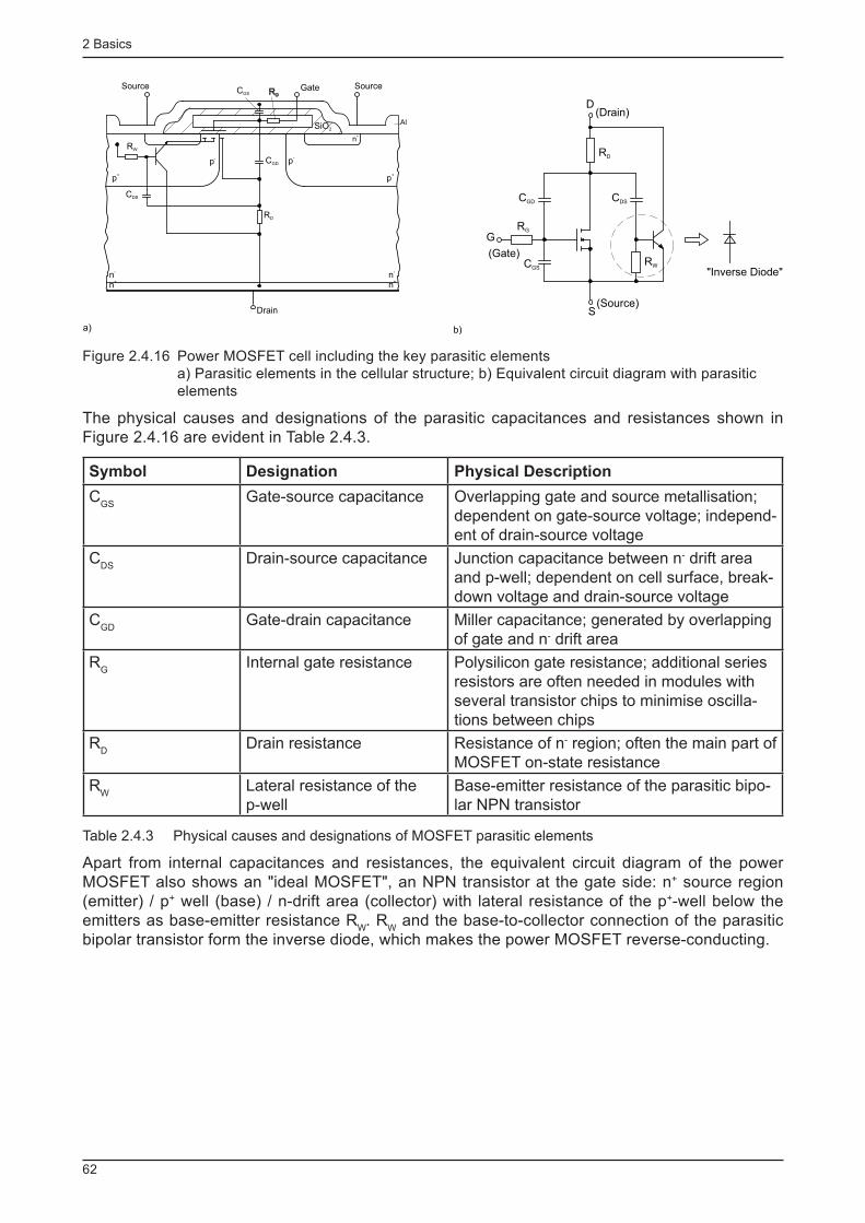
2 Basics
62
S
(Source)
(Drain)D
G
(Gate)
"Inverse Diode"
RD
RW
CDSCGD
RG
CGS
n+
Gate Source
SiO2
p+
Al
n+
p-
Source
p+
n-
n+
n-
Drain
p-
RW
RD
RG
CGD
CGS
CDS
a) b)
Figure 2.4.16 Power MOSFET cell including the key parasitic elements a) Parasitic elements in the cellular structure; b) Equivalent circuit diagram with parasitic elements
The physical causes and designations of the parasitic capacitances and resistances shown in Figure 2.4.16 are evident in Table 2.4.3.
Symbol Designation Physical Description
C GS
Gate-source capacitance Overlapping gate and source metallisation; dependent on gate-source voltage; independ-ent of drain-source voltage
C DS
Drain-source capacitance Junction capacitance between n - drift area and p-well; dependent on cell surface, break-down voltage and drain-source voltage
C GD
Gate-drain capacitance Miller capacitance; generated by overlapping of gate and n - drift area
R G
Internal gate resistance Polysilicon gate resistance; additional series resistors are often needed in modules with several transistor chips to minimise oscilla-tions between chips
R D
Drain resistance Resistance of n - region; often the main part of MOSFET on-state resistance
R W
Lateral resistance of the p-well
Base-emitter resistance of the parasitic bipo-lar NPN transistor
Table 2.4.3 Physical causes and designations of MOSFET parasitic elements
Apart from internal capacitances and resistances, the equivalent circuit diagram of the power MOSFET also shows an "ideal MOSFET", an NPN transistor at the gate side: n + source region (emitter) / p + well (base) / n-drift area (collector) with lateral resistance of the p + -well below the emitters as base-emitter resistance R
W . R
W and the base-to-collector connection of the parasitic
bipolar transistor form the inverse diode, which makes the power MOSFET reverse-conducting.
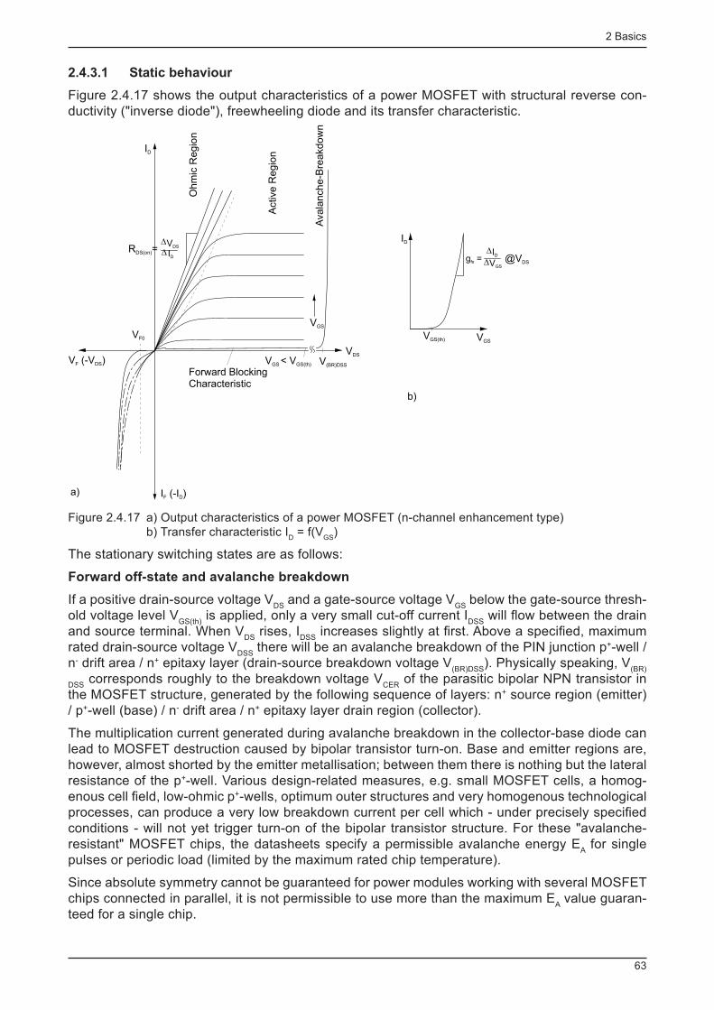
2 Basics
63
2.4.3.1 Static behaviour
Figure 2.4.17 shows the output characteristics of a power MOSFET with structural reverse con-ductivity ("inverse diode"), freewheeling diode and its transfer characteristic.
Forward BlockingCharacteristic
V < VGS GS(th)
I (-I )F D
V(BR)DSSV (-V )F DS
Avala
nche-B
reakdow
n
Oh
mic
Re
gio
n
Active R
egio
n
ID
VGS
R =DS(on)
VDS?
ID
ID
VGSVGS(th)
g =fs
ID?VGS
?
VDS
@VDS
a)
b)
?
VF0
Figure 2.4.17 a) Output characteristics of a power MOSFET (n-channel enhancement type) b) Transfer characteristic I
D = f(V
GS )
The stationary switching states are as follows:
Forward off-state and avalanche breakdown
If a positive drain-source voltage V DS
and a gate-source voltage V GS
below the gate-source thresh-old voltage level V
GS(th) is applied, only a very small cut-off current I
DSS will fl ow between the drain
and source terminal. When V DS
rises, I DSS
increases slightly at fi rst. Above a specifi ed, maximum rated drain-source voltage V
DSS there will be an avalanche breakdown of the PIN junction p + -well /
n - drift area / n + epitaxy layer (drain-source breakdown voltage V (BR)DSS
). Physically speaking, V (BR)
DSS corresponds roughly to the breakdown voltage V
CER of the parasitic bipolar NPN transistor in
the MOSFET structure, generated by the following sequence of layers: n + source region (emitter) / p + -well (base) / n - drift area / n + epitaxy layer drain region (collector).
The multiplication current generated during avalanche breakdown in the collector-base diode can lead to MOSFET destruction caused by bipolar transistor turn-on. Base and emitter regions are, however, almost shorted by the emitter metallisation; between them there is nothing but the lateral resistance of the p + -well. Various design-related measures, e.g. small MOSFET cells, a homog-enous cell fi eld, low-ohmic p + -wells, optimum outer structures and very homogenous technological processes, can produce a very low breakdown current per cell which - under precisely specifi ed conditions - will not yet trigger turn-on of the bipolar transistor structure. For these "avalanche-resistant" MOSFET chips, the datasheets specify a permissible avalanche energy E
A for single
pulses or periodic load (limited by the maximum rated chip temperature).
Since absolute symmetry cannot be guaranteed for power modules working with several MOSFET chips connected in parallel, it is not permissible to use more than the maximum E
A value guaran-
teed for a single chip.
2 Basics
64
On-state (1st quadrant)
The forward on-state at a positive drain-source voltage V DS
and positive drain current I D comprises
two characteristic curve areas:
Active region (pinch-off area)
With a gate-emitter voltage V GE
that hardly exceeds the gate-emitter threshold voltage V GE(th)
, a relatively high voltage share will be depleted through the channel owing to current saturation (hori-zontal part of the output characteristics). The drain current I
D is controlled by V
GS . As a measure for
the transfer behaviour as described in Figure 2.4.17b) the forward transconductance g fs is defi ned
as
g fs = ∆I
D /∆V
GS = I
D /(V
GS -V
GS(th) ).
Forward transconductance rises in proportion to the increase in drain current I D and the drain-
source voltage V DS
and falls as chip temperature increases. In the switching mode that is exclu-sively permissible for power modules working with several MOSFET chips connected in parallel, the pinch-off area is only run through during turn-on and turn-off. Stationary module operation in the pinch-off area is not permissible, because V
GS(th) drops when the temperature rises, meaning
that even small differences between the individual chips may cause thermal instability.
Ohmic characteristic area
The ohmic characteristic area (steep part of the output characteristics), which corresponds to ON-state during switching operations, is reached when I
D is determined by the outer circuit only. On-
state behaviour is charaterised by the drain-source on-resistance R DS(on)
as a quotient of changing drain-source voltage V
DS and drain current I
D . The on-resistance R
DS(on) is dependent on the gate-
source voltage V GS
and the chip temperature. In the operating temperature range of a MOSFET, R
DS(on) is almost doubled in the range between 25°C and 125°C, cf. chapter 3.4.3.
Inverse operation (3rd quadrant)
In inverse mode, the MOSFET has a diode characteristic at V GS
< V GS(th)
(continuous curve in Fig-ure 2.4.17). This behaviour is caused by the parasitic diode in the MOSFET structure; the on-state voltage of the collector-(source)-base-(drain)-pn-junction ("inverse diode"). The bipolar current fl ow through this diode determines the on-state behaviour of the MOSFET in reverse direction, when the channel is closed (Figure 2.4.18a).
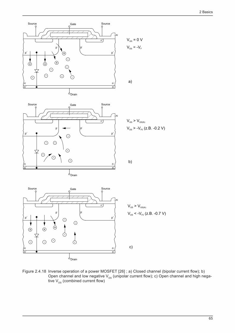
2 Basics
65
n+
Gate Source
p+
Al
n+
p-
Source
p+
n-
n+
n-
Drain
p-
n+
Gate Source
p+
Al
n+
p-
Source
p+
n-
n+
n-
Drain
p-
n+
Gate Source
p+
Al
n+
p-
Source
p+
n-
n+
n-
Drain
p-
+
+
-
-
-
-
V = 0 VGS
V = -VDS F
a)
V > VGS GS(th)
V > -V (z.B. -0.2 V)DS F0
b)
- -
--
-
-
-
--
-
--
-
++
-
+
V > VGS GS(th)
V < -V (z.B. -0.7 V)DS F0
c)
++
-- -
Figure 2.4.18 Inverse operation of a power MOSFET [26] ; a) Closed channel (bipolar current fl ow); b) Open channel and low negative V
DS (unipolar current fl ow); c) Open channel and high nega-
tive V DS
(combined current fl ow)
2 Basics
66
Generally speaking, the bipolar inverse diode can be utilised within the current limits specifi ed for the MOSFET. Practice, however, often shows that - inverse diodes cause relatively high on-state losses which must be dissipated together with the MOSFET losses and
- that the poor turn-off behaviour and relatively low dv/dt limits of these PIN diodes are responsi-ble for the practical application limits of MOSFET bridge circuits in processes that require hard switching.
As shown in Figure 2.4.18, the MOSFET channel can also be conductively controlled when a negative drain-source voltage is present, provided that a gate-source voltage is applied above the threshold voltage level.
If the drain-source voltage is then externally limited - e.g. by connecting a Schottky diode in par-allel - to values below the threshold voltage of the inverse diode, the inverse current will remain a unipolar electron fl ow (majority carrier fl ow) from drain to source. Consequently, the switching behaviour corresponds to that of MOSFET. The inverse current depends on -V
DS and V
GS (Figure
2.4.18b).
Operation according to Figure 2.4.18c occurs, if the channel is additionally controlled while the bi-polar inverse diode is conducting (drain-source voltage above threshold voltage level). This results in a lower on-state voltage than for a simple parallel connection for diode and MOSFET, since the injected charge carriers laterally diffuse as well, thus improving MOSFET conductivity.
Today, this behaviour is made use of in low-voltage power supply systems, where "synchronous rectifi ers" with integrated MOSFET can be used instead of conventional diode rectifi ers. If MOS-FET are triggered during the conducting phase of their inverse diode, switch-mode power supplies with < 15 V output voltage, for example, may substantially gain in effi ciency owing to the extremely low on-state voltage (some 10 mV) compared to conventional diode rectifying (on-state voltage several 100 mV).
2.4.3.2 Switching behaviour
The switching behaviour (switching velocity, losses) of MOSFET power modules is determined by their structural, internal capacitances and the internal and terminal resistances. Contrary to the ideal of powerless voltage control via the MOSFET gate, frequency-dependent control power is required; this is owing to the recharge currents of the internal capacitances which are needed for switching. Furthermore, the commutation processes are affected by the parasitic connection inductances present in the components and connections and generated by connecting transistor chips in power modules; they induce transient overvoltages and may cause oscillations due to the circuit and transistor capacitances, cf. chapter 5.
The switching behaviour of power MOSFET can be described as resulting from the transistor's internal capacitances and resistances:
When the MOSFET is turned off, C GD
is low and approximately equal to C DS
.
During on-state, C GD
will increase rapidly as soon as the gate-source voltage has exceeded the drain-source voltage; this is due to inversion in the enhancement layer below the gate regions.
Datasheets (cf. chapter 3.4.3) normally list the low-signal capacitances C iss
, C rss
and C oss
of the turned-off transistor, see Table 2.4.4.
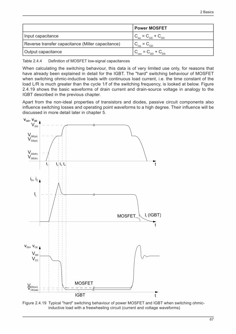
2 Basics
67
Power MOSFET
Input capacitance C iss
= C GS
+ C GD
Reverse transfer capacitance (Miller capacitance) C rss
= C GD
Output capacitance C oss
= C GD
+ C DS
Table 2.4.4 Defi nition of MOSFET low-signal capacitances
When calculating the switching behaviour, this data is of very limited use only, for reasons that have already been explained in detail for the IGBT. The "hard" switching behaviour of MOSFET when switching ohmic-inductive loads with continuous load current, i.e. the time constant of the load L/R is much greater than the cycle 1/f of the switching frequency, is looked at below. Figure 2.4.19 shows the basic waveforms of drain current and drain-source voltage in analogy to the IGBT described in the previous chapter.
Apart from the non-ideal properties of transistors and diodes, passive circuit components also infl uence switching losses and operating point waveforms to a high degree. Their infl uence will be discussed in more detail later in chapter 5.
VGG
v , vGS GE
VGS(th)
VGE(th)
t1 t2 t3 t4
i , iD C
IL
I (IGBT)t
v , vDS CE
VV
DD
CC
VDS(on)VCE(sat)
MOSFET
IGBT
t
t
MOSFET
t
VGE(pl)
VGS(pl)
Figure 2.4.19 Typical "hard" switching behaviour of power MOSFET and IGBT when switching ohmic-inductive load with a freewheeling circuit (current and voltage waveforms)
2 Basics
68
Turn-on
As Figure 2.4.19 demonstrates, the drain-source voltage of the power MOSFET drops to the on-
state voltage value within some 10 ns DS(on)DDS(on) RIV ×= .
Turn-on: switching interval 0...t 1 (blocked transistor)
The gate current i G starts fl owing when the control voltage is applied. At fi rst, i
G charges only the
gate capacitance C GS
until it reaches the charge quantity Q G1
; the gate-source voltage V GS
rises in line with the time constant determined by the input capacitance of the MOSFET and the gate resistance. Since V
GS is still below the threshold voltage V
GS(th) , no collector current will fl ow during
this period.
Turn-on: switching interval t 1 ...t
2 (drain current rise)
After the threshold voltage V GS(th)
(t 1 ) has been reached, the drain current will start to rise. Similarly,
V GS
, which is connected to the drain current in the MOSFET pinch-off area by means of the rate of rise g
fs with I
D = g
fs · V
GS , will increase up to the value V
GS1 = I
D /g
fs (time t
2 ). Since the freewheeling
diode can block the current at t 2 only, V
DS will not drop signifi cantly before t
2 is reached. At t = t
2 ,
charge Q G2
will have fl owed into the gate.
The largest amount of turn-on losses is generated in the MOSFET during this time interval. As long as the i
D value is still below I
L and part of I
L still has to fl ow through the freewheeling diode,
the drain-source voltage v DS
cannot drop far below the operating voltage V DD
during this period. The difference between V
DD and V
DS outlined in Figure 2.4.19 is mainly caused by transient voltage
drops across the parasitic inductances of the commutation circuit.
Turn-on: switching interval t 2 ...t
3 (transistor fully switched on in the pinch-off area)
When the freewheeling diode is turned off, V DS
drops to the on-state value until t
3
DS(on)DDS(on) RIV ×= has been reached. Between t 2 and t
3 , drain current and gate-source
voltage are still coupled through the transconductance: V GS
remains roughly con-stant. While v
DS drops, the gate current i
G recharges the Miller capacitance C
DG with the
charge (Q G3
-Q G2
). By t = t 3 , an amount of charge equal to Q
G3 will have fl owed into the gate.
After the entire load current I L has been commutated to the MOSFET, the freewheeling diode will
start to block. Owing to the reverse recovery time of the freewheeling diode, the MOSFET drain current i
D initially continues to rise above I
L during turn-off of the freewheeling diode (t
rr ) by the
amount I RRM
of the diode reverse current and dissipates the reverse recovery charge Q rr of the
freewheeling diode. For explanations of the characteristics I RRM
, Q rr and E
rr for inverse diodes, see
chapter 3.4.2.
Turn-on: switching interval t 3 ...t
4 (ohmic operating area)
At t 3 , the MOSFET is now turned on and its operating point has passed through the pinch-off area
and has reached the border of the ohmic operating area. V GS
and I D are no longer coupled by g
fs .
The charge quantity (Q Gtot
-Q G3
) now supplied to the gate causes the further rise in V GS
up to the level of the gate control voltage V
GG .
Turn-off
During turn-off, the processes described above run in reverse direction. Charge Q Gtot
has to be discharged from the gate with the aid of the gate current. In contrast to IGBT, power MOSFET do not use a negative gate voltage here but V
GS = 0 V, see chapter 5.
During turn-off only the internal capacitances of the power MOSFET have to be recharged to such an extent that there is no charge carrier infl uence left in the channel area. From this point on, neu-trality interference in this area will quickly be reduced and the drain current will drop rapidly. The overshoot of v
DS over V
DD indicated in Figure 2.4.19 results mainly from the parasitic inductances
of the commutation circuit and increases in proportion to the turn-off speed -di D /dt of the power
MOSFET.Likewise in the case of power MOSFET: the more the specifi c transistor application deviates from the "ideal hard switch" application described here, the more "blurry" the step-form of the gate-

2 Basics
69
source voltage curve becomes. The intervals "decoupled" during hard switching will then merge more and more, and any description of the switching behaviour becomes more complex.
2.4.3.3 Latest versions and new directions of development
Power electronics largely use the vertical structure shown in Figure 2.4.3, where gate and source terminals are located on the chip surface and the drain terminal is on the underside of the chip. The load current is conducted vertically through the chip outside the channel. The VD MOSFET version ( V ertical D ouble D iffused MOSFET) introduced at the beginning of the eighties is still be-ing used today and is being continuously improved on, e.g. reduction in cell dimensions. Depend-ing on the application focus on "low" or "high" drain-source voltage, the key developments on the power MOSFET front have gone in two directions with signifi cant structural differences:
Trench-Gate MOSFET
The example shown in Figure 2.4.20 illustrates the continuous development towards the Trench-MOSFET, which was introduced around 1997.
Figure 2.4.20 a) conventional VDMOSFET; b) MOSFET with trench-gate (Trench MOSFET) [27]
Similar to the development of the Trench IGBT, the insulated gate plates - and thus the channel area - are arranged vertically here; the distance to be covered by the electrons in the n-region is thus shorter. This enables a signifi cant reduction in R
DS(on) mainly in the lower voltage range com-
pared to conventional structures.
Superjunction MOSFET
As mentioned at the beginning of this chapter, the "breakthrough" achieved in the reduction of R
DS(on) was initiated in 1999 by Infi neon with the development of the CoolMOS as the fi rst "Super-
junction" power MOSFET on the market.The compensation principle used in superjunction components was developed for MOSFET with blocking voltages between 500 V and 1000 V. Figure 2.4.21 demonstrates the layout and func-tional principle of a CoolMOS.

2 Basics
70
Figure 2.4.21 Layout and functional principle of a superjunction MOSFET (CoolMOS) [25]
With the aid of several epitaxy steps or lateral diffusion from trenches, high-doped conducting col-umns are injected into the low-doped n - drift area. These columns are connected with the p-wells. Column doping is dimensioned such that the n-doping of the drift area is compensated for, result-ing in a very low effective doping level.
In blocking state, the fi eld is almost rectangular and can take up the maximum voltage level in rela-tion to the thickness of the n- - region. Drift area doping can only be increased to such an extent that still allows for it to be compensated by the same amount of doping in the p-column ("compensation principle"). This overrides the interdependency of blocking voltage and doping density [17].
As a result, the thickness of the n - drift area can be reduced substantially compared to conven-tional MOSFET, and drift area conductivity can be increased by way of higher doping. This means that the on-resistance R
DS(on) will no longer increase to the power of 2.4...2.6, but almost linear to
the breakdown voltage V (BR)DSS
; the on-state losses of high-blocking power MOSFET can be re-duced signifi cantly (to 1/3 - 1/5). Chip area, switching losses and gate capacitance / gate charge drop accordingly – for the same current capability. Figure 2.4.22 shows the differences in layout and properties for standard and superjunction power MOSFET.
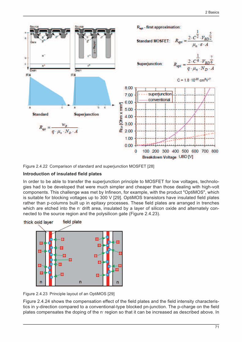
2 Basics
71
Figure 2.4.22 Comparison of standard and superjunction MOSFET [28]
Introduction of insulated fi eld plates
In order to be able to transfer the superjunction principle to MOSFET for low voltages, technolo-gies had to be developed that were much simpler and cheaper than those dealing with high-volt components. This challenge was met by Infi neon, for example, with the product "OptiMOS", which is suitable for blocking voltages up to 300 V [29]. OptiMOS transistors have insulated fi eld plates rather than p-columns built up in epitaxy processes. These fi eld plates are arranged in trenches which are etched into the n - drift area, insulated by a layer of silicon oxide and alternately con-nected to the source region and the polysilicon gate (Figure 2.4.23).
Figure 2.4.23 Principle layout of an OptiMOS [29]
Figure 2.4.24 shows the compensation effect of the fi eld plates and the fi eld intensity characteris-tics in y-direction compared to a conventional-type blocked pn-junction. The p-charge on the fi eld plates compensates the doping of the n - region so that it can be increased as described above. In
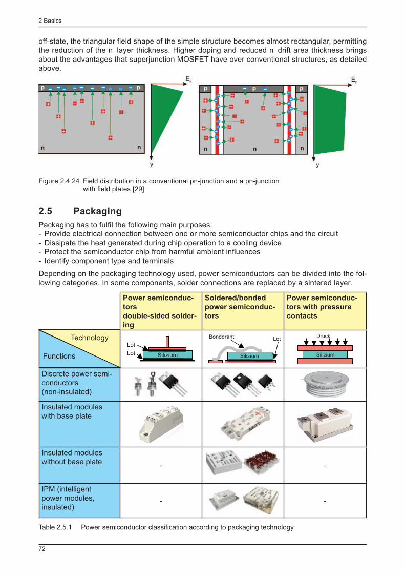
2 Basics
72
off-state, the triangular fi eld shape of the simple structure becomes almost rectangular, permitting the reduction of the n - layer thickness. Higher doping and reduced n - drift area thickness brings about the advantages that superjunction MOSFET have over conventional structures, as detailed above.
Figure 2.4.24 Field distribution in a conventional pn-junction and a pn-junction with fi eld plates [29]
2.5 Packaging
Packaging has to fulfi l the following main purposes: - Provide electrical connection between one or more semiconductor chips and the circuit - Dissipate the heat generated during chip operation to a cooling device - Protect the semiconductor chip from harmful ambient infl uences - Identify component type and terminals
Depending on the packaging technology used, power semiconductors can be divided into the fol-lowing categories. In some components, solder connections are replaced by a sintered layer.
Power semiconduc-
tors
double-sided solder-
ing
Soldered/bonded
power semiconduc-
tors
Power semiconduc-
tors with pressure
contacts
Silizium
Lot
Lot
Bonddraht Lot
Silizium Silizium
Druck
Discrete power semi-conductors (non-insulated)
Insulated modules with base plate
Insulated modules without base plate -
-
IPM (intelligent power modules, insulated)
-
-
Table 2.5.1 Power semiconductor classifi cation according to packaging technology
Technology
Functions

2 Basics
73
Innovations in packaging technology focus on a number of areas, including: - Improvement of heat dissipation and thermal cycling capability - Minimisation of inductances in the module and in the supply leads by means of suitable module designs
- Highly fl exible packaging, easy customer assembly - Greater degree of integration (converter circuits) - Integration of monitoring, protection and driver functions
2.5.1 Technologies
2.5.1.1 Soldering
Soldering is the connection of two (metal) materials by means of liquid metal or a liquid alloy. In-dividual atoms in the solder then diffuse into the metal surface of the components to be soldered and a thin layer of an alloy made of solder and substrate is created. The prerequisite for void-free soldering quality are clean surfaces free from oxide for all connection components involved. For this purpose, fl uxing agents are often used to clean surfaces; these agents are activated when the materials are warmed up for soldering. They also protect the surfaces from re-oxidation during soldering. Most fl uxing agents must be removed again after soldering. Reducing gases, such as inert gas, can be used as fl uxing agents. Applying a vacuum as soon as the solder has liquefi ed is a very good way of achieving void-free connections. Solder connections must conform with the RoHS Directive (Restriction of Hazardous Substances Directive) of the European Union.
A wide variety of soldering processes are available and are mainly distinguished by the manner in which heat is coupled to the part to be soldered. An interesting process method is the use of soldering pastes consisting of little solder balls and a paste-like fl uxing agent. Using a dispenser, by screen or stencil printing, the paste is applied onto one of connection parts; the second partner (e.g. the chip) is pressed into the paste and the connection is heated until the solder melts (refl ow soldering).
Large-area solder connections between materials with very different thermal expansion coeffi -cients are critical (Table 2.5.4). The bimetal effect causes bending and, under thermal cycling, solder fatigue which will ultimately result in solder failure. For this reason it is not possible to solder large-area ceramic parts onto copper base plates, for example.
2.5.1.2 Diffusion sintering (low-temperature joining technology)
Diffusion sintering is a process which can replace soldering in many cases. It may be considered as being far superior to soldering in terms of its long-term reliability. At a temperature of around 250°C, fi ne silver powder is sintered under high pressure to form a low-porous silver bond layer (Figure 2.5.1) between the parts to be connected.
Figure 2.5.1 Silver powder before and after diffusion sintering
Sintered layers are stable up to the melting point of silver (962°C). Fluxing agent is not required. Sintered layers display better thermal, mechanical and electrical properties than solder (Table 2.5.2).
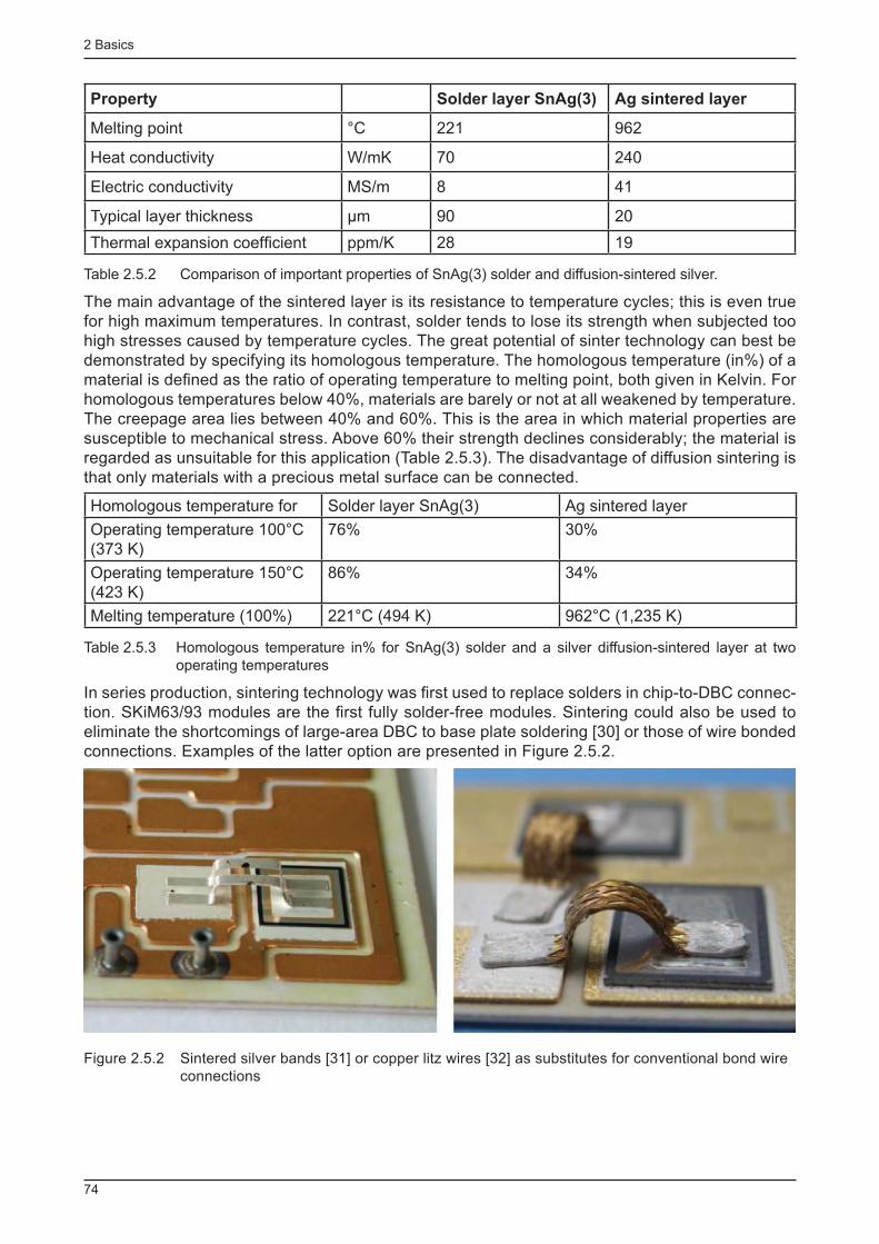
2 Basics
74
Property Solder layer SnAg(3) Ag sintered layer
Melting point °C 221 962
Heat conductivity W/mK 70 240
Electric conductivity MS/m 8 41
Typical layer thickness µm 90 20
Thermal expansion coeffi cient ppm/K 28 19
Table 2.5.2 Comparison of important properties of SnAg(3) solder and diffusion-sintered silver.
The main advantage of the sintered layer is its resistance to temperature cycles; this is even true for high maximum temperatures. In contrast, solder tends to lose its strength when subjected too high stresses caused by temperature cycles. The great potential of sinter technology can best be demonstrated by specifying its homologous temperature. The homologous temperature (in%) of a material is defi ned as the ratio of operating temperature to melting point, both given in Kelvin. For homologous temperatures below 40%, materials are barely or not at all weakened by temperature. The creepage area lies between 40% and 60%. This is the area in which material properties are susceptible to mechanical stress. Above 60% their strength declines considerably; the material is regarded as unsuitable for this application (Table 2.5.3). The disadvantage of diffusion sintering is that only materials with a precious metal surface can be connected.
Homologous temperature for Solder layer SnAg(3) Ag sintered layer
Operating temperature 100°C (373 K)
76% 30%
Operating temperature 150°C (423 K)
86% 34%
Melting temperature (100%) 221°C (494 K) 962°C (1,235 K)
Table 2.5.3 Homologous temperature in% for SnAg(3) solder and a silver diffusion-sintered layer at two operating temperatures
In series production, sintering technology was fi rst used to replace solders in chip-to-DBC connec-tion. SKiM63/93 modules are the fi rst fully solder-free modules. Sintering could also be used to eliminate the shortcomings of large-area DBC to base plate soldering [30] or those of wire bonded connections. Examples of the latter option are presented in Figure 2.5.2.
Figure 2.5.2 Sintered silver bands [31] or copper litz wires [32] as substitutes for conventional bond wire connections
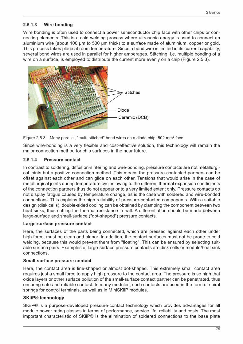
2 Basics
75
2.5.1.3 Wire bonding
Wire bonding is often used to connect a power semiconductor chip face with other chips or con-necting elements. This is a cold welding process where ultrasonic energy is used to connect an aluminium wire (about 100 µm to 500 µm thick) to a surface made of aluminium, copper or gold. This process takes place at room temperature. Since a bond wire is limited in its current capability, several bond wires are used in parallel for higher amperages. Stitching, i.e. multiple bonding of a wire on a surface, is employed to distribute the current more evenly on a chip (Figure 2.5.3).
Stitches
Diode
Ceramic (DCB)
Figure 2.5.3 Many parallel, "multi-stitched" bond wires on a diode chip, 502 mm² face.
Since wire-bonding is a very fl exible and cost-effective solution, this technology will remain the major connection method for chip surfaces in the near future.
2.5.1.4 Pressure contact
In contrast to soldering, diffusion-sintering and wire-bonding, pressure contacts are not metallurgi-cal joints but a positive connection method. This means the pressure-contacted partners can be offset against each other and can glide on each other. Tensions that would arise in the case of metallurgical joints during temperature cycles owing to the different thermal expansion coeffi cients of the connection partners thus do not appear or to a very limited extent only. Pressure contacts do not display fatigue caused by temperature change, as is the case with soldered and wire-bonded connections. This explains the high reliability of pressure-contacted components. With a suitable design (disk cells), double-sided cooling can be obtained by clamping the component between two heat sinks, thus cutting the thermal resistance in half. A differentiation should be made between large-surface and small-surface ("dot-shaped") pressure contacts.
Large-surface pressure contact
Here, the surfaces of the parts being connected, which are pressed against each other under high force, must be clean and planar. In addition, the contact surfaces must not be prone to cold welding, because this would prevent them from "fl oating". This can be ensured by selecting suit-able surface pairs. Examples of large-surface pressure contacts are disk cells or module/heat sink connections.
Small-surface pressure contact
Here, the contact area is line-shaped or almost dot-shaped. This extremely small contact area requires just a small force to apply high pressure to the contact area. The pressure is so high that oxide layers or other surface pollution of the small-surface contact partner can be penetrated, thus ensuring safe and reliable contact. In many modules, such contacts are used in the form of spiral springs for control terminals, as well as in MiniSKiiP modules.
SKiiP® technology
SKiiP® is a purpose-developed pressure-contact technology which provides advantages for all module power rating classes in terms of performance, service life, reliability and costs. The most important characteristic of SKiiP® is the elimination of soldered connections to the base plate
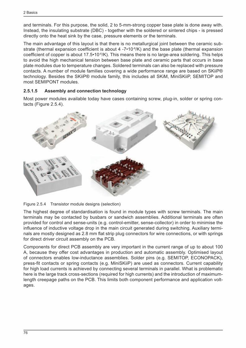
2 Basics
76
and terminals. For this purpose, the solid, 2 to 5-mm-strong copper base plate is done away with. Instead, the insulating substrate (DBC) - together with the soldered or sintered chips - is pressed directly onto the heat sink by the case, pressure elements or the terminals.
The main advantage of this layout is that there is no metallurgical joint between the ceramic sub-strate (thermal expansion coeffi cient is about 4 -7•10 -6 /K) and the base plate (thermal expansion coeffi cient of copper is about 17.5•10 -6 /K). This means there is no large-area soldering. This helps to avoid the high mechanical tension between base plate and ceramic parts that occurs in base plate modules due to temperature changes. Soldered terminals can also be replaced with pressure contacts. A number of module families covering a wide performance range are based on SKiiP® technology. Besides the SKiiP® module family, this includes all SKiM, MiniSKiiP, SEMITOP and most SEMIPONT modules.
2.5.1.5 Assembly and connection technology
Most power modules available today have cases containing screw, plug-in, solder or spring con-tacts (Figure 2.5.4).
Figure 2.5.4 Transistor module designs (selection)
The highest degree of standardisation is found in module types with screw terminals. The main terminals may be contacted by busbars or sandwich assemblies. Additional terminals are often provided for control and sense-units (e.g. control-emitter, sense-collector) in order to minimise the infl uence of inductive voltage drop in the main circuit generated during switching. Auxiliary termi-nals are mostly designed as 2.8 mm fl at strip plug connectors for wire connections, or with springs for direct driver circuit assembly on the PCB.
Components for direct PCB assembly are very important in the current range of up to about 100 A, because they offer cost advantages in production and automatic assembly. Optimised layout of connectors enables low-inductance assemblies. Solder pins (e.g. SEMITOP, ECONOPACK), press-fi t contacts or spring contacts (e.g. MiniSKiiP) are used as connectors. Current capability for high load currents is achieved by connecting several terminals in parallel. What is problematic here is the large track cross-sections (required for high currents) and the introduction of maximum-length creepage paths on the PCB. This limits both component performance and application volt-ages.

2 Basics
77
The merits of spring contacts
Figure 2.5.5 Spring types for main and auxiliary contacts
Spring contacts have a number of advantages over solder and press-fi t contacts with respect to PCB assembly. - Better utilisation of the PCB area and easier routing, since "vias" are not required - Easier assembly automation, since no large-surface components with tolerances have to be fi t-ted into holes
- Assembly of the (heavy and expensive) power semiconductor and heat sink after soldering and PCB pre-testing
- Improved thermal cycling capability thanks to "free-moving" contacts - Higher resistance to shock and vibration stress (no solder fatigue) - Quasi-hermetically sealed contact is corrosion-proof - No electromigration
Mechanical natural frequencies: The spring weight is so low that their natural frequencies (> 1 kHz) are far higher the mechanical oscillations produced in "heavy" power modules.
Figure 2.5.6 Natural frequency analysis of a non-loaded spring with a 1.1 kHz resonance frequency in Z-direction
Contact force: The spring contact contact force is about 2…10 kN/cm². This ensures safe and reliable contact even under shock stress of up to 100 G (SKiM63/93). This is within the range for screw connections and far higher than for plug-in contacts.

2 Basics
78
Figure 2.5.7 Comparison of contact pressures of detachable electrical connections (from left to right: screw, plug-in, spring contact)
Inductances: The inductance of a MiniSKiiP spring (Figure 2.5.5) only insignifi cantly higher than the one of a solder pin. Spiral springs, as used in the control circuit of SEMiX, SKiM and SKiiP, have a higher inductance. This lies within the range of 100 nH.
nH112Dl4
DnL
22
2 =+
×p××m=
µ=µ 0 =1.26 µH/m;
l=10 mm (length, pressed); D=2 mm (inner diameter); n=17 (number of windings);
This can be compared to connection wires of 10 cm in length, as are common in auxiliary terminals in modules with plug-in contacts. If the driver board is directly connected via the spiral springs, the total inductance composed of inner and outer inductance in the control circuit is even far lower than the wire-contacted interfacing of standard modules.
Figure 2.5.8 Control terminals of a SEMITRANS module (a) and a SEMiX module (b)
Landing Pad requirements: The springs have a silver-plated surface, the PCB landing pads must be tin-plated (chemically: Sn, HAL-Sn Hot Air Leveling) or coated with nickel / gold fl ash (>3 µ Ni, > 20 nm Au).
2.5.1.6 Modules with or without base plate
Some comparisons are rather inaccurate (e.g. [33]) since they compare the two technologies by examining a module with base plate to begin with and then simply removing the base plate to per-form the comparison. Of course, both design variants must be constructed under totally different aspects. SEMIKRON offers both technologies, because both have advantages and disadvantages.

2 Basics
79
Base plate
Such modules are charaterised by the use of few large chips with good heat spreading through the base plate.
Advantages: - Mechanically more robust during transport and assembly - Larger thermal mass, lower thermal impedance within the range of 1 s
Disadvantages of modules with soldered or bonded chips (IGBT modules): - Higher thermal resistance chip / heat sink R
th(j-s) , because base plate bending requires a thicker
layer of thermal paste - Reduced slow power cycling capability, since the large-area base plate solder pads are suscep-tible to temperature cycles
- Higher internal terminal resistances (r cc’-ee’
), since, for thermo-mechanical reasons, the design is based on small ceramic substrates that require additional internal connectors
- Increased weight
No base plate
Such modules use smaller chips and achieve thermal spreading on the heat sink thanks to heat sources which are better spread.
Advantages: - Lower thermal resistance, because layers are omitted, even contact with the heat sink, thinner thermal paste layers
- Improved thermal cycling capability, because of removal of solder fatigue in base plate soldering (bec. no base plate!)
- Smaller chips; lower temperature gradient over the chip means a lower maximum temperature and less stress under power cycling conditions
- Few large ceramic substrates with low terminal resistance
Disadvantages - No heat storage - Processable chip size is limited, resulting in more parallel connections - Increased requirements for thermal paste application
Eliminating the thermo-mechanical stress between base plate and ceramic substrate, rather than connecting several small substrates soldered onto a common base plate into one circuit with the aid of additional connection elements, enables very large ceramic substrates to be used in mod-ules with no base plate (Figure 2.5.9).
Figure 2.5.9 Large DBC substrate (115 mm x 80 mm), equipped with the chips of a 350 A / 1200 V IGBT three-phase bridge and angle connectors
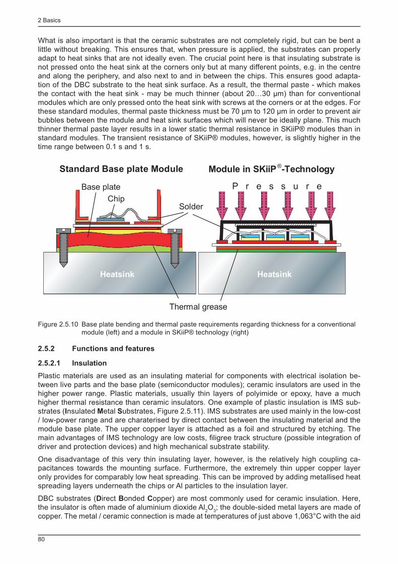
2 Basics
80
What is also important is that the ceramic substrates are not completely rigid, but can be bent a little without breaking. This ensures that, when pressure is applied, the substrates can properly adapt to heat sinks that are not ideally even. The crucial point here is that insulating substrate is not pressed onto the heat sink at the corners only but at many different points, e.g. in the centre and along the periphery, and also next to and in between the chips. This ensures good adapta-tion of the DBC substrate to the heat sink surface. As a result, the thermal paste - which makes the contact with the heat sink - may be much thinner (about 20…30 µm) than for conventional modules which are only pressed onto the heat sink with screws at the corners or at the edges. For these standard modules, thermal paste thickness must be 70 µm to 120 µm in order to prevent air bubbles between the module and heat sink surfaces which will never be ideally plane. This much thinner thermal paste layer results in a lower static thermal resistance in SKiiP® modules than in standard modules. The transient resistance of SKiiP® modules, however, is slightly higher in the time range between 0.1 s and 1 s.
Module in SKiiP®-TechnologyStandard Base plate Module
Thermal grease
Chip
Heat sink
P r e s s u r e
Chip
Base plate
Solder
Heatsink Heatsink
a) b)Figure 2.5.10 Base plate bending and thermal paste requirements regarding thickness for a conventional
module (left) and a module in SKiiP® technology (right)
2.5.2 Functions and features
2.5.2.1 Insulation
Plastic materials are used as an insulating material for components with electrical isolation be-tween live parts and the base plate (semiconductor modules); ceramic insulators are used in the higher power range. Plastic materials, usually thin layers of polyimide or epoxy, have a much higher thermal resistance than ceramic insulators. One example of plastic insulation is IMS sub-strates ( I nsulated M etal S ubstrates, Figure 2.5.11). IMS substrates are used mainly in the low-cost / low-power range and are charaterised by direct contact between the insulating material and the module base plate. The upper copper layer is attached as a foil and structured by etching. The main advantages of IMS technology are low costs, fi ligree track structure (possible integration of driver and protection devices) and high mechanical substrate stability.
One disadvantage of this very thin insulating layer, however, is the relatively high coupling ca-pacitances towards the mounting surface. Furthermore, the extremely thin upper copper layer only provides for comparably low heat spreading. This can be improved by adding metallised heat spreading layers underneath the chips or Al particles to the insulation layer.
DBC substrates ( D irect B onded C opper) are most commonly used for ceramic insulation. Here, the insulator is often made of aluminium dioxide Al
2 O
3 ; the double-sided metal layers are made of
copper. The metal / ceramic connection is made at temperatures of just above 1,063°C with the aid
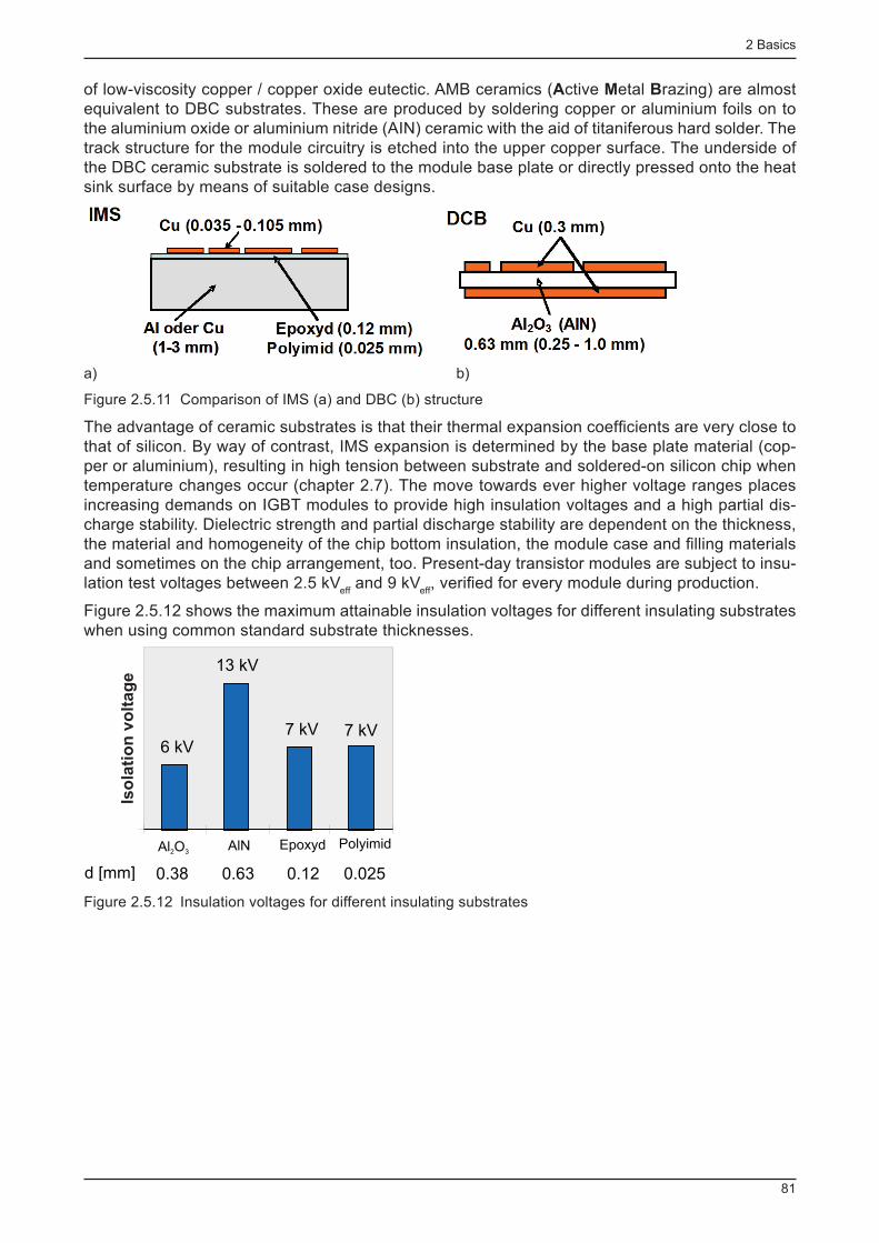
2 Basics
81
of low-viscosity copper / copper oxide eutectic. AMB ceramics ( A ctive M etal B razing) are almost equivalent to DBC substrates. These are produced by soldering copper or aluminium foils on to the aluminium oxide or aluminium nitride (AIN) ceramic with the aid of titaniferous hard solder. The track structure for the module circuitry is etched into the upper copper surface. The underside of the DBC ceramic substrate is soldered to the module base plate or directly pressed onto the heat sink surface by means of suitable case designs.
a) b)
Figure 2.5.11 Comparison of IMS (a) and DBC (b) structure
The advantage of ceramic substrates is that their thermal expansion coeffi cients are very close to that of silicon. By way of contrast, IMS expansion is determined by the base plate material (cop-per or aluminium), resulting in high tension between substrate and soldered-on silicon chip when temperature changes occur (chapter 2.7). The move towards ever higher voltage ranges places increasing demands on IGBT modules to provide high insulation voltages and a high partial dis-charge stability. Dielectric strength and partial discharge stability are dependent on the thickness, the material and homogeneity of the chip bottom insulation, the module case and fi lling materials and sometimes on the chip arrangement, too. Present-day transistor modules are subject to insu-lation test voltages between 2.5 kV
eff and 9 kV
eff , verifi ed for every module during production.
Figure 2.5.12 shows the maximum attainable insulation voltages for different insulating substrates when using common standard substrate thicknesses.
6 kV7 kV 7 kV
13 kV
Al O2 3AlN Epoxyd Polyimid
d [mm] 0.38 0.63 0.12 0.025
Iso
lati
on
vo
lta
ge
Figure 2.5.12 Insulation voltages for different insulating substrates
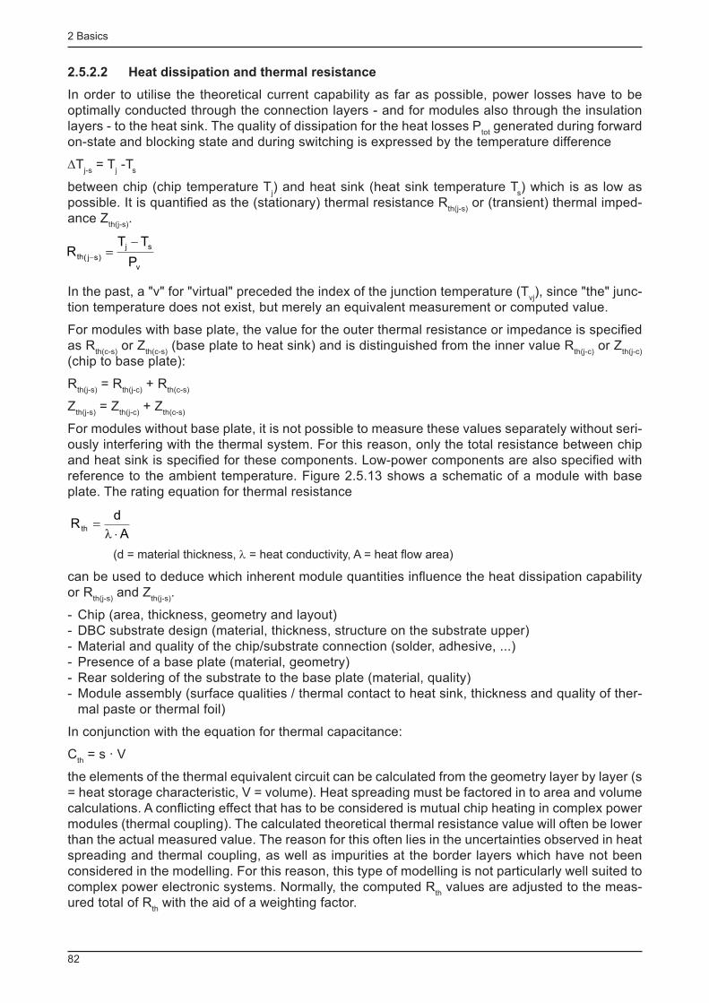
2 Basics
82
2.5.2.2 Heat dissipation and thermal resistance
In order to utilise the theoretical current capability as far as possible, power losses have to be optimally conducted through the connection layers - and for modules also through the insulation layers - to the heat sink. The quality of dissipation for the heat losses P
tot generated during forward
on-state and blocking state and during switching is expressed by the temperature difference
∆T j-s
= T j -T
s
between chip (chip temperature T j ) and heat sink (heat sink temperature T
s ) which is as low as
possible. It is quantifi ed as the (stationary) thermal resistance R th(j-s)
or (transient) thermal imped-ance Z
th(j-s) .
v
sj
)sj(thP
TTR
-=-
In the past, a "v" for "virtual" preceded the index of the junction temperature (T vj ), since "the" junc-
tion temperature does not exist, but merely an equivalent measurement or computed value.
For modules with base plate, the value for the outer thermal resistance or impedance is specifi ed as R
th(c-s) or Z
th(c-s) (base plate to heat sink) and is distinguished from the inner value R
th(j-c) or Z
th(j-c)
(chip to base plate):
R th(j-s)
= R th(j-c)
+ R th(c-s)
Z th(j-s)
= Z th(j-c)
+ Z th(c-s)
For modules without base plate, it is not possible to measure these values separately without seri-ously interfering with the thermal system. For this reason, only the total resistance between chip and heat sink is specifi ed for these components. Low-power components are also specifi ed with reference to the ambient temperature. Figure 2.5.13 shows a schematic of a module with base plate. The rating equation for thermal resistance
A
dR th ×l
=
(d = material thickness, λ = heat conductivity, A = heat fl ow area)
can be used to deduce which inherent module quantities infl uence the heat dissipation capability or R
th(j-s) and Z
th(j-s) .
- Chip (area, thickness, geometry and layout) - DBC substrate design (material, thickness, structure on the substrate upper) - Material and quality of the chip/substrate connection (solder, adhesive, ...) - Presence of a base plate (material, geometry) - Rear soldering of the substrate to the base plate (material, quality) - Module assembly (surface qualities / thermal contact to heat sink, thickness and quality of ther-mal paste or thermal foil)
In conjunction with the equation for thermal capacitance:
C th = s · V
the elements of the thermal equivalent circuit can be calculated from the geometry layer by layer (s = heat storage characteristic, V = volume). Heat spreading must be factored in to area and volume calculations. A confl icting effect that has to be considered is mutual chip heating in complex power modules (thermal coupling). The calculated theoretical thermal resistance value will often be lower than the actual measured value. The reason for this often lies in the uncertainties observed in heat spreading and thermal coupling, as well as impurities at the border layers which have not been considered in the modelling. For this reason, this type of modelling is not particularly well suited to complex power electronic systems. Normally, the computed R
th values are adjusted to the meas-
ured total of R th with the aid of a weighting factor.
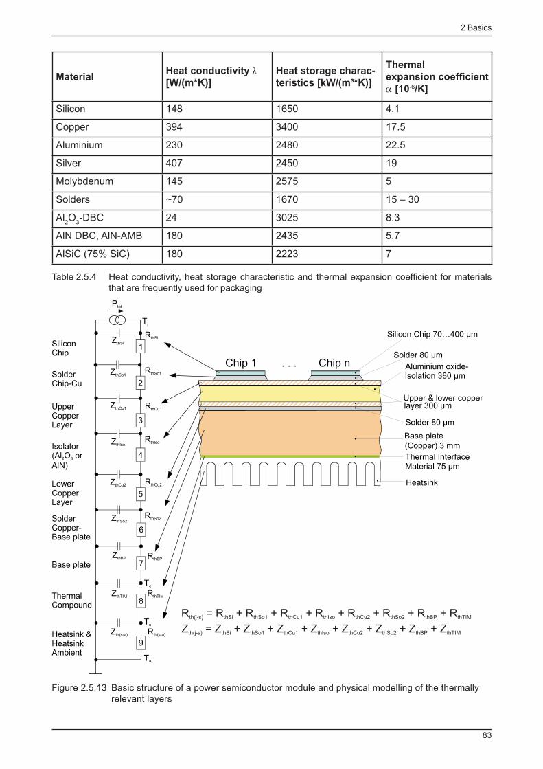
2 Basics
83
Material Heat conductivity λ
[W/(m*K)]
Heat storage charac-
teristics [kW/(m³*K)]
Thermal
expansion coeffi cient
α [10 -6 /K]
Silicon 148 1650 4.1
Copper 394 3400 17.5
Aluminium 230 2480 22.5
Silver 407 2450 19
Molybdenum 145 2575 5
Solders ~70 1670 15 – 30
Al 2 O
3 -DBC 24 3025 8.3
AlN DBC, AlN-AMB 180 2435 5.7
AlSiC (75% SiC) 180 2223 7
Table 2.5.4 Heat conductivity, heat storage characteristic and thermal expansion coeffi cient for materials that are frequently used for packaging
Silicon Chip 70…400 µm
Solder 80 µmChip 1 Chip n. . . Aluminium oxide-
Isolation 380 µm
Upper & lower copperlayer 300 µm
Solder 80 µm
1
2
3
4
5
6
7
8
9
Ptot
ZthSi
Tj
ZthSo1
ZthCu1
ZthIso
ZthSo2
ZthBP
ZthTIM
Zth(s-a)
ZthCu2
SiliconChip
SolderChip-Cu
UpperCopperLayer
Isolator(Al O or
AlN)2 3
LowerCopperLayer
SolderCopper-Base plate
Base plate
ThermalCompound
Heatsink &HeatsinkAmbient
Base plate
(Copper) 3 mm
Thermal InterfaceMaterial 75 µm
Heatsink
Tc
RthSi
RthSo1
RthCu1
RthIso
RthCu2
RthSo2
RthBP
RthTIM
Ts
Rth(s-a)
Ta
R = R + R + R + R + R + R + R + Rth(j-s) thSi thSo1 thCu1 thIso thCu2 thSo2 thBP thTIM
Z = Z + Z + Z + Z + Z + Z + Z + Zth(j-s) thSi thSo1 thCu1 thIso thCu2 thSo2 thBP thTIM
Figure 2.5.13 Basic structure of a power semiconductor module and physical modelling of the thermally relevant layers
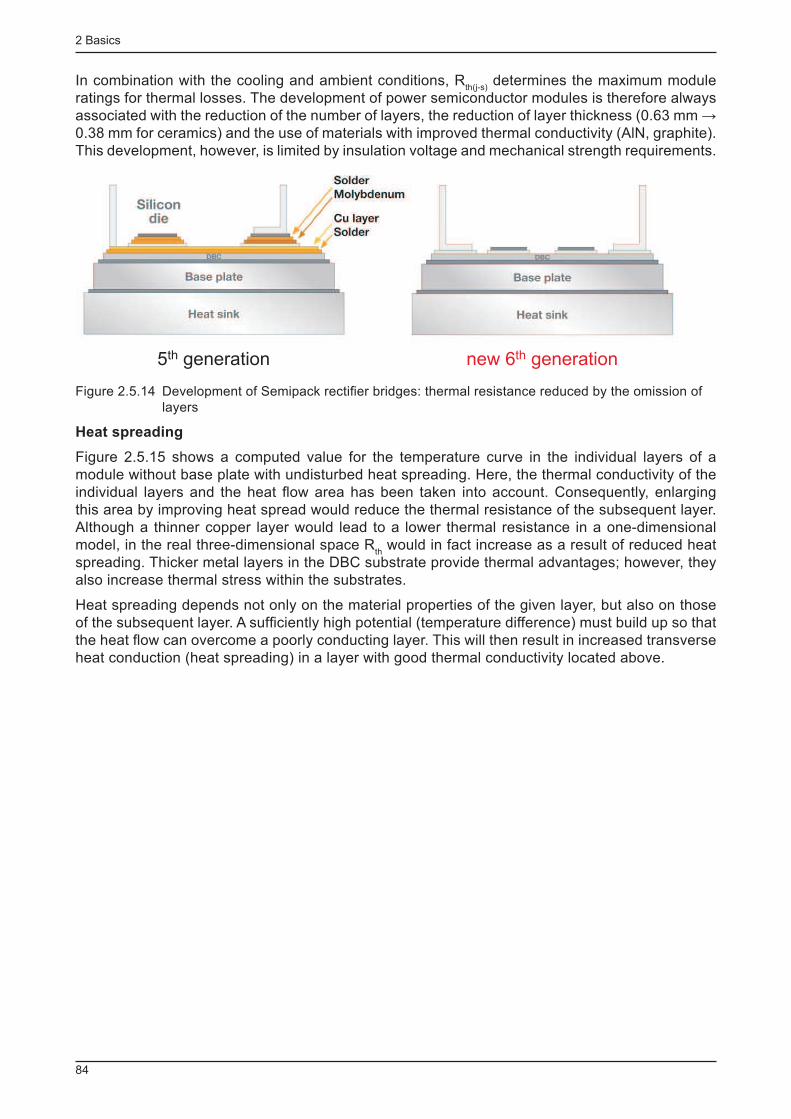
2 Basics
84
In combination with the cooling and ambient conditions, R th(j-s)
determines the maximum module ratings for thermal losses. The development of power semiconductor modules is therefore always associated with the reduction of the number of layers, the reduction of layer thickness (0.63 mm → 0.38 mm for ceramics) and the use of materials with improved thermal conductivity (AlN, graphite). This development, however, is limited by insulation voltage and mechanical strength requirements.
5th generation
9 layers
new 6th generation
5 layersFigure 2.5.14 Development of Semipack rectifi er bridges: thermal resistance reduced by the omission of
layers
Heat spreading
Figure 2.5.15 shows a computed value for the temperature curve in the individual layers of a module without base plate with undisturbed heat spreading. Here, the thermal conductivity of the individual layers and the heat fl ow area has been taken into account. Consequently, enlarging this area by improving heat spread would reduce the thermal resistance of the subsequent layer. Although a thinner copper layer would lead to a lower thermal resistance in a one-dimensional model, in the real three-dimensional space R
th would in fact increase as a result of reduced heat
spreading. Thicker metal layers in the DBC substrate provide thermal advantages; however, they also increase thermal stress within the substrates.
Heat spreading depends not only on the material properties of the given layer, but also on those of the subsequent layer. A suffi ciently high potential (temperature difference) must build up so that the heat fl ow can overcome a poorly conducting layer. This will then result in increased transverse heat conduction (heat spreading) in a layer with good thermal conductivity located above.
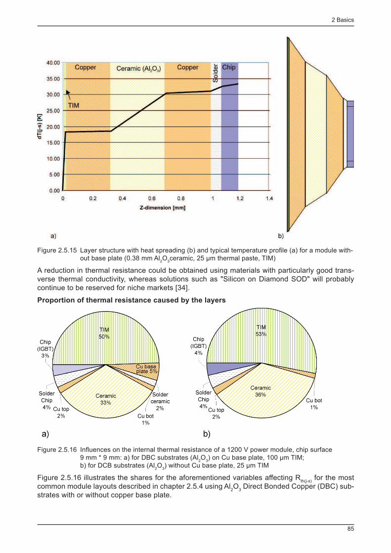
2 Basics
85
Figure 2.5.15 Layer structure with heat spreading (b) and typical temperature profi le (a) for a module with-out base plate (0.38 mm Al
2 O
3 ceramic, 25 µm thermal paste, TIM)
A reduction in thermal resistance could be obtained using materials with particularly good trans-verse thermal conductivity, whereas solutions such as "Silicon on Diamond SOD" will probably continue to be reserved for niche markets [34].
Proportion of thermal resistance caused by the layers
Figure 2.5.16 Infl uences on the internal thermal resistance of a 1200 V power module, chip surface 9 mm * 9 mm: a) for DBC substrates (Al
2 O
3 ) on Cu base plate, 100 µm TIM;
b) for DCB substrates (Al 2 O
3 ) without Cu base plate, 25 µm TIM
Figure 2.5.16 illustrates the shares for the aforementioned variables affecting R th(j-s)
for the most common module layouts described in chapter 2.5.4 using Al
2 O
3 Direct Bonded Copper (DBC) sub-
strates with or without copper base plate.
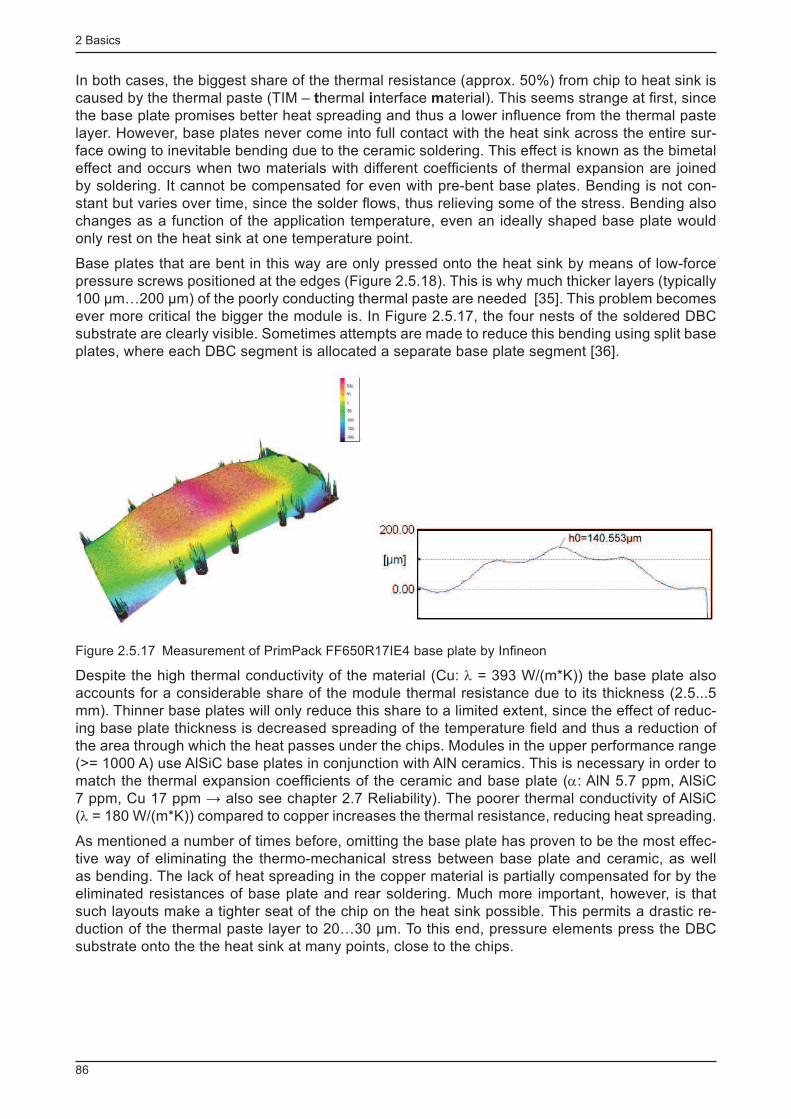
2 Basics
86
In both cases, the biggest share of the thermal resistance (approx. 50%) from chip to heat sink is caused by the thermal paste (TIM – t hermal i nterface m aterial). This seems strange at fi rst, since the base plate promises better heat spreading and thus a lower infl uence from the thermal paste layer. However, base plates never come into full contact with the heat sink across the entire sur-face owing to inevitable bending due to the ceramic soldering. This effect is known as the bimetal effect and occurs when two materials with different coeffi cients of thermal expansion are joined by soldering. It cannot be compensated for even with pre-bent base plates. Bending is not con-stant but varies over time, since the solder fl ows, thus relieving some of the stress. Bending also changes as a function of the application temperature, even an ideally shaped base plate would only rest on the heat sink at one temperature point.
Base plates that are bent in this way are only pressed onto the heat sink by means of low-force pressure screws positioned at the edges (Figure 2.5.18). This is why much thicker layers (typically 100 µm…200 µm) of the poorly conducting thermal paste are needed [35]. This problem becomes ever more critical the bigger the module is. In Figure 2.5.17, the four nests of the soldered DBC substrate are clearly visible. Sometimes attempts are made to reduce this bending using split base plates, where each DBC segment is allocated a separate base plate segment [36].
Figure 2.5.17 Measurement of PrimPack FF650R17IE4 base plate by Infi neon
Despite the high thermal conductivity of the material (Cu: λ = 393 W/(m*K)) the base plate also accounts for a considerable share of the module thermal resistance due to its thickness (2.5...5 mm). Thinner base plates will only reduce this share to a limited extent, since the effect of reduc-ing base plate thickness is decreased spreading of the temperature fi eld and thus a reduction of the area through which the heat passes under the chips. Modules in the upper performance range (>= 1000 A) use AlSiC base plates in conjunction with AlN ceramics. This is necessary in order to match the thermal expansion coeffi cients of the ceramic and base plate (α: AlN 5.7 ppm, AlSiC 7 ppm, Cu 17 ppm → also see chapter 2.7 Reliability). The poorer thermal conductivity of AlSiC (λ = 180 W/(m*K)) compared to copper increases the thermal resistance, reducing heat spreading.
As mentioned a number of times before, omitting the base plate has proven to be the most effec-tive way of eliminating the thermo-mechanical stress between base plate and ceramic, as well as bending. The lack of heat spreading in the copper material is partially compensated for by the eliminated resistances of base plate and rear soldering. Much more important, however, is that such layouts make a tighter seat of the chip on the heat sink possible. This permits a drastic re-duction of the thermal paste layer to 20…30 µm. To this end, pressure elements press the DBC substrate onto the the heat sink at many points, close to the chips.
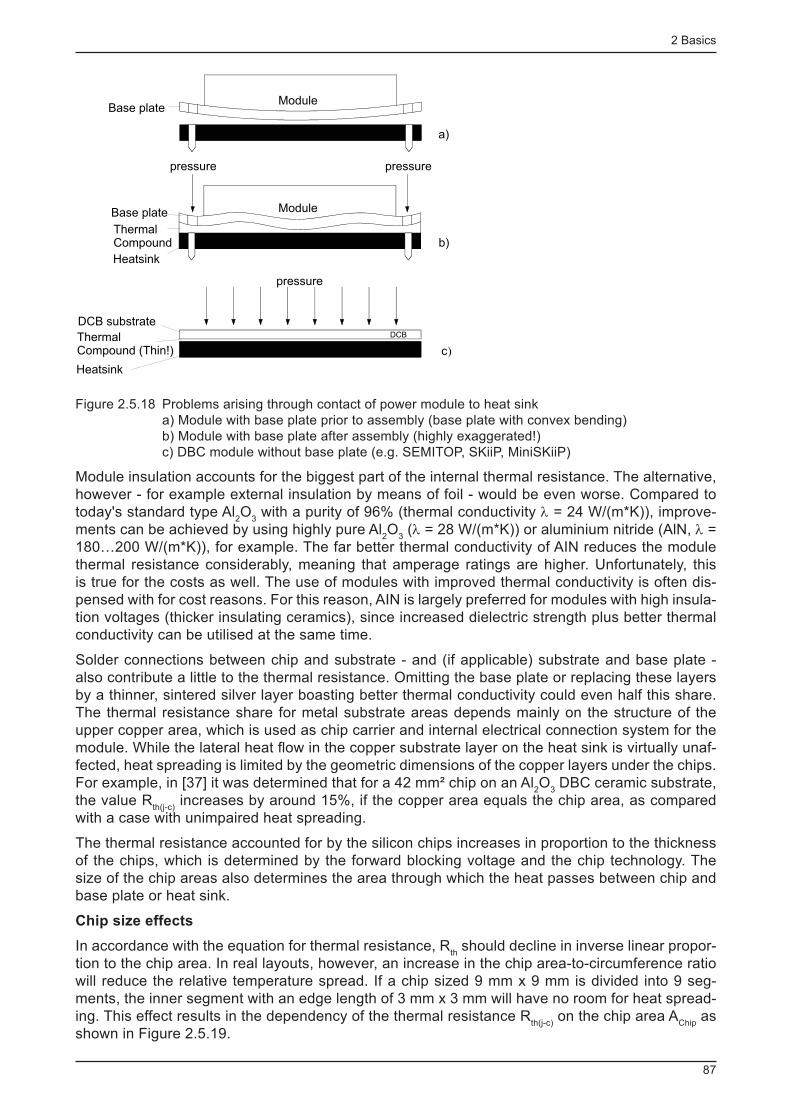
2 Basics
87
ModuleBase plate
ModuleBase plate
DCB substrate
pressure pressure
DCB
pressure
ThermalCompound
Heatsink
a)
b)
c)
ThermalCompound (Thin!)
Heatsink
Figure 2.5.18 Problems arising through contact of power module to heat sinka) Module with base plate prior to assembly (base plate with convex bending)b) Module with base plate after assembly (highly exaggerated!)c) DBC module without base plate (e.g. SEMITOP, SKiiP, MiniSKiiP)
Module insulation accounts for the biggest part of the internal thermal resistance. The alternative, however - for example external insulation by means of foil - would be even worse. Compared to today's standard type Al
2 O
3 with a purity of 96% (thermal conductivity λ = 24 W/(m*K)), improve-
ments can be achieved by using highly pure Al 2 O
3 (λ = 28 W/(m*K)) or aluminium nitride (AlN, λ =
180…200 W/(m*K)), for example. The far better thermal conductivity of AIN reduces the module thermal resistance considerably, meaning that amperage ratings are higher. Unfortunately, this is true for the costs as well. The use of modules with improved thermal conductivity is often dis-pensed with for cost reasons. For this reason, AIN is largely preferred for modules with high insula-tion voltages (thicker insulating ceramics), since increased dielectric strength plus better thermal conductivity can be utilised at the same time.
Solder connections between chip and substrate - and (if applicable) substrate and base plate - also contribute a little to the thermal resistance. Omitting the base plate or replacing these layers by a thinner, sintered silver layer boasting better thermal conductivity could even half this share. The thermal resistance share for metal substrate areas depends mainly on the structure of the upper copper area, which is used as chip carrier and internal electrical connection system for the module. While the lateral heat fl ow in the copper substrate layer on the heat sink is virtually unaf-fected, heat spreading is limited by the geometric dimensions of the copper layers under the chips. For example, in [37] it was determined that for a 42 mm² chip on an Al
2 O
3 DBC ceramic substrate,
the value R th(j-c)
increases by around 15%, if the copper area equals the chip area, as compared with a case with unimpaired heat spreading.
The thermal resistance accounted for by the silicon chips increases in proportion to the thickness of the chips, which is determined by the forward blocking voltage and the chip technology. The size of the chip areas also determines the area through which the heat passes between chip and base plate or heat sink.
Chip size effects
In accordance with the equation for thermal resistance, R th should decline in inverse linear propor-
tion to the chip area. In real layouts, however, an increase in the chip area-to-circumference ratio will reduce the relative temperature spread. If a chip sized 9 mm x 9 mm is divided into 9 seg-ments, the inner segment with an edge length of 3 mm x 3 mm will have no room for heat spread-ing. This effect results in the dependency of the thermal resistance R
th(j-c) on the chip area A
Chip as
shown in Figure 2.5.19.
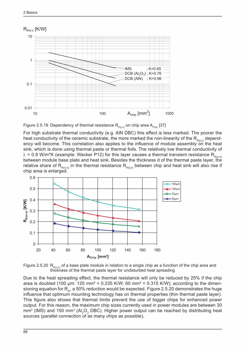
2 Basics
88
0.01
0.1
1
10
10 100
IMS ; K=0.65
DCB (Al2O3) ; K=0.76
DCB (AlN) ; K=0.96
Rth/j-c [K/W]
Achip [mm2] 1000
Figure 2.5.19 Dependency of thermal resistance R th(j-c)
on chip area A Chip
[37]
For high substrate thermal conductivity (e.g. AlN DBC) this effect is less marked. The poorer the heat conductivity of the ceramic substrate, the more marked the non-linearity of the R
th(j-c) depend-
ency will become. This correlation also applies to the infl uence of module assembly on the heat sink, which is done using thermal paste or thermal foils. The relatively low thermal conductivity of λ = 0.8 W/m*K (example: Wacker P12) for this layer causes a thermal transient resistance R
th(c-s)
between module base plate and heat sink. Besides the thickness d of the thermal paste layer, the relative share of R
th(c-s) in the thermal resistance R
th(j-s) between chip and heat sink will also rise if
chip area is enlarged.
0
0.1
0.2
0.3
0.4
0.5
0.6
20 40 60 80 100 120 140 160 180
AChip [mm²]
Rth
(c-s
)[K
/W]
150µm
100µm
75µm
50µm
Figure 2.5.20 R th(c-s)
of a base plate module in relation to a single chip as a function of the chip area and thickness of the thermal paste layer for undisturbed heat spreading
Due to the heat spreading effect, the thermal resistance will only be reduced by 25% if the chip area is doubled (100 µm: 120 mm² = 0.235 K/W; 60 mm² = 0.315 K/W); according to the dimen-sioning equation for R
th , a 50% reduction would be expected. Figure 2.5.20 demonstrates the huge
infl uence that optimum mounting technology has on thermal properties (thin thermal paste layer). This fi gure also shows that thermal limits prevent the use of bigger chips for enhanced power output. For this reason, the maximum chip sizes currently used in power modules are between 30 mm 2 (IMS) and 150 mm 2 (Al
2 O
3 DBC). Higher power output can be reached by distributing heat
sources (parallel connection of as many chips as possible).
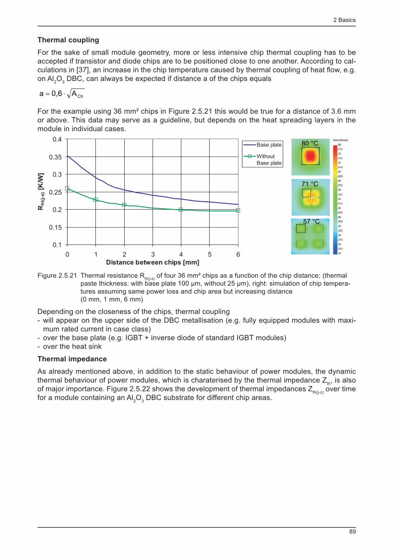
2 Basics
89
Thermal coupling
For the sake of small module geometry, more or less intensive chip thermal coupling has to be accepted if transistor and diode chips are to be positioned close to one another. According to cal-culations in [37], an increase in the chip temperature caused by thermal coupling of heat fl ow, e.g. on Al
2 O
3 DBC, can always be expected if distance a of the chips equals
ChA0,6a ×=
For the example using 36 mm² chips in Figure 2.5.21 this would be true for a distance of 3.6 mm or above. This data may serve as a guideline, but depends on the heat spreading layers in the module in individual cases.
0.1
0.15
0.2
0.25
0.3
0.35
0.4
0 1 2 3 4 5 6
Distance between chips [mm]
Rh
t(j-
s)
[K/W
]
Base plate
Without
Base plate
80 °C
71 °C
57 °C
Figure 2.5.21 Thermal resistance R th(j-s)
of four 36 mm² chips as a function of the chip distance; (thermal paste thickness: with base plate 100 µm, without 25 µm), right: simulation of chip tempera-tures assuming same power loss and chip area but increasing distance (0 mm, 1 mm, 6 mm)
Depending on the closeness of the chips, thermal coupling - will appear on the upper side of the DBC metallisation (e.g. fully equipped modules with maxi-mum rated current in case class)
- over the base plate (e.g. IGBT + inverse diode of standard IGBT modules) - over the heat sink
Thermal impedance
As already mentioned above, in addition to the static behaviour of power modules, the dynamic thermal behaviour of power modules, which is charaterised by the thermal impedance Z
th , is also
of major importance. Figure 2.5.22 shows the development of thermal impedances Z th(j-c)
over time for a module containing an Al
2 O
3 DBC substrate for different chip areas.
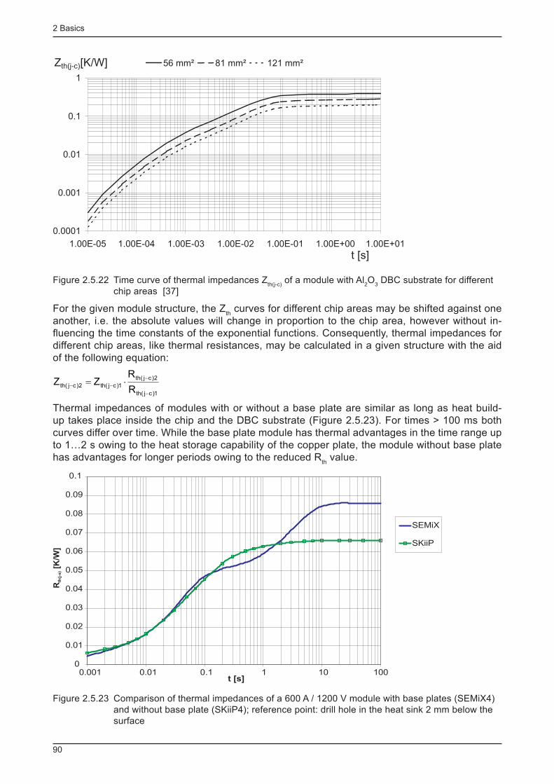
2 Basics
90
0.0001
0.001
0.01
0.1
1
1.00E-05 1.00E-04 1.00E-03 1.00E-02 1.00E-01 1.00E+00 1.00E+01
56 mm² 81 mm² 121 mm²
t [s]
Zth(j-c)[K/W]
Figure 2.5.22 Time curve of thermal impedances Z th(j-c)
of a module with Al 2 O
3 DBC substrate for different
chip areas [37]
For the given module structure, the Z th curves for different chip areas may be shifted against one
another, i.e. the absolute values will change in proportion to the chip area, however without in-fl uencing the time constants of the exponential functions. Consequently, thermal impedances for different chip areas, like thermal resistances, may be calculated in a given structure with the aid of the following equation:
1)cj(th
2)cj(th
1)cj(th2)cj(thR
RZZ
-
--- ×=
Thermal impedances of modules with or without a base plate are similar as long as heat build-up takes place inside the chip and the DBC substrate (Figure 2.5.23). For times > 100 ms both curves differ over time. While the base plate module has thermal advantages in the time range up to 1…2 s owing to the heat storage capability of the copper plate, the module without base plate has advantages for longer periods owing to the reduced R
th value.
0
0.01
0.02
0.03
0.04
0.05
0.06
0.07
0.08
0.09
0.1
0.001 0.01 0.1 1 10 100t [s]
SEMiX
SKiiP
R[K
/W]
th(j
-s)
Figure 2.5.23 Comparison of thermal impedances of a 600 A / 1200 V module with base plates (SEMiX4) and without base plate (SKiiP4); reference point: drill hole in the heat sink 2 mm below the surface
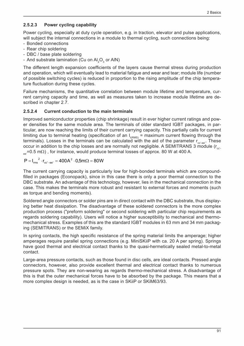
2 Basics
91
2.5.2.3 Power cycling capability
Power cycling, especially at duty cycle operation, e.g. in traction, elevator and pulse applications, will subject the internal connections in a module to thermal cycling, such connections being: - Bonded connections - Rear chip soldering - DBC / base plate soldering - And substrate lamination (Cu on Al
2 O
3 or AlN)
The different length expansion coeffi cients of the layers cause thermal stress during production and operation, which will eventually lead to material fatigue and wear and tear; module life (number of possible switching cycles) is reduced in proportion to the rising amplitude of the chip tempera-ture fl uctuation during these cycles.
Failure mechanisms, the quantitative correlation between module lifetime and temperature, cur-rent carrying capacity and time, as well as measures taken to increase module lifetime are de-scribed in chapter 2.7.
2.5.2.4 Current conduction to the main terminals
Improved semiconductor properties (chip shrinkage) result in ever higher current ratings and pow-er densities for the same module area. The terminals of older standard IGBT packages, in par-ticular, are now reaching the limits of their current carrying capacity. This partially calls for current limiting due to terminal heating (specifi cation of an I
t(RMS) = maximum current fl owing through the
terminals). Losses in the terminals can be calculated with the aid of the parameter r cc’-ee’
. These occur in addition to the chip losses and are normally not negligible. A SEMITRANS 3 module (r
cc’-
ee’ =0.5 mΩ) , for instance, would produce terminal losses of approx. 80 W at 400 A.
W80m5,0A400rIP 2
'ee'cc
2
rms =W×=×= -
The current carrying capacity is particularly low for high-bonded terminals which are compound-fi lled in packages (Econopack), since in this case there is only a poor thermal connection to the DBC substrate. An advantage of this technology, however, lies in the mechanical connection in the case. This makes the terminals more robust and resistant to external forces and moments (such as torque and bending moments).
Soldered angle connectors or solder pins are in direct contact with the DBC substrate, thus display-ing better heat dissipation. The disadvantage of these soldered connectors is the more complex production process ("preform soldering" or second soldering with particular chip requirements as regards soldering capability). Users will notice a higher susceptibility to mechanical and thermo-mechanical stress. Examples of this are the standard IGBT modules in 63 mm and 34 mm packag-ing (SEMITRANS) or the SEMiX family.
In spring contacts, the high specifi c resistance of the spring material limits the amperage; higher amperages require parallel spring connections (e.g. MiniSKiiP with ca. 20 A per spring). Springs have good thermal and electrical contact thanks to the quasi-hermetically sealed metal-to-metal contact.
Large-area pressure contacts, such as those found in disc cells, are ideal contacts. Pressed angle connectors, however, also provide excellent thermal and electrical contact thanks to numerous pressure spots. They are non-wearing as regards thermo-mechanical stress. A disadvantage of this is that the outer mechanical forces have to be absorbed by the package. This means that a more complex design is needed, as is the case in SKiiP or SKiM63/93.
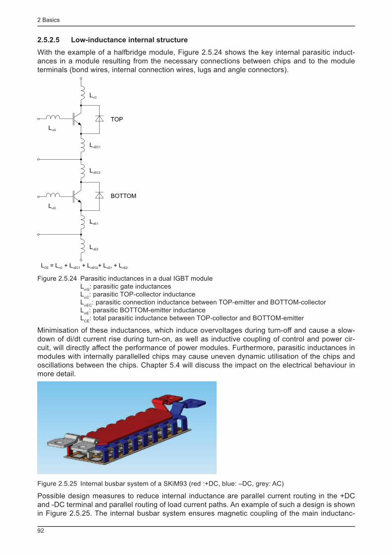
2 Basics
92
2.5.2.5 Low-inductance internal structure
With the example of a halfbridge module, Figure 2.5.24 shows the key internal parasitic induct-ances in a module resulting from the necessary connections between chips and to the module terminals (bond wires, internal connection wires, lugs and angle connectors).
LsEC1
LsE1
TOP
BOTTOM
LsC
LsEC2
LsE2
LsG
LsG
L = L + L + L + L + LCE C EC1 EC2 E1 E2s s s s s
Figure 2.5.24 Parasitic inductances in a dual IGBT moduleL
σG : parasitic gate inductances
L σC
: parasitic TOP-collector inductanceL
σEC : parasitic connection inductance between TOP-emitter and BOTTOM-collector
L σE
: parasitic BOTTOM-emitter inductanceL
CE : total parasitic inductance between TOP-collector and BOTTOM-emitter
Minimisation of these inductances, which induce overvoltages during turn-off and cause a slow-down of di/dt current rise during turn-on, as well as inductive coupling of control and power cir-cuit, will directly affect the performance of power modules. Furthermore, parasitic inductances in modules with internally parallelled chips may cause uneven dynamic utilisation of the chips and oscillations between the chips. Chapter 5.4 will discuss the impact on the electrical behaviour in more detail.
Figure 2.5.25 Internal busbar system of a SKiM93 (red :+DC, blue: –DC, grey: AC)
Possible design measures to reduce internal inductance are parallel current routing in the +DC and -DC terminal and parallel routing of load current paths. An example of such a design is shown in Figure 2.5.25. The internal busbar system ensures magnetic coupling of the main inductanc-
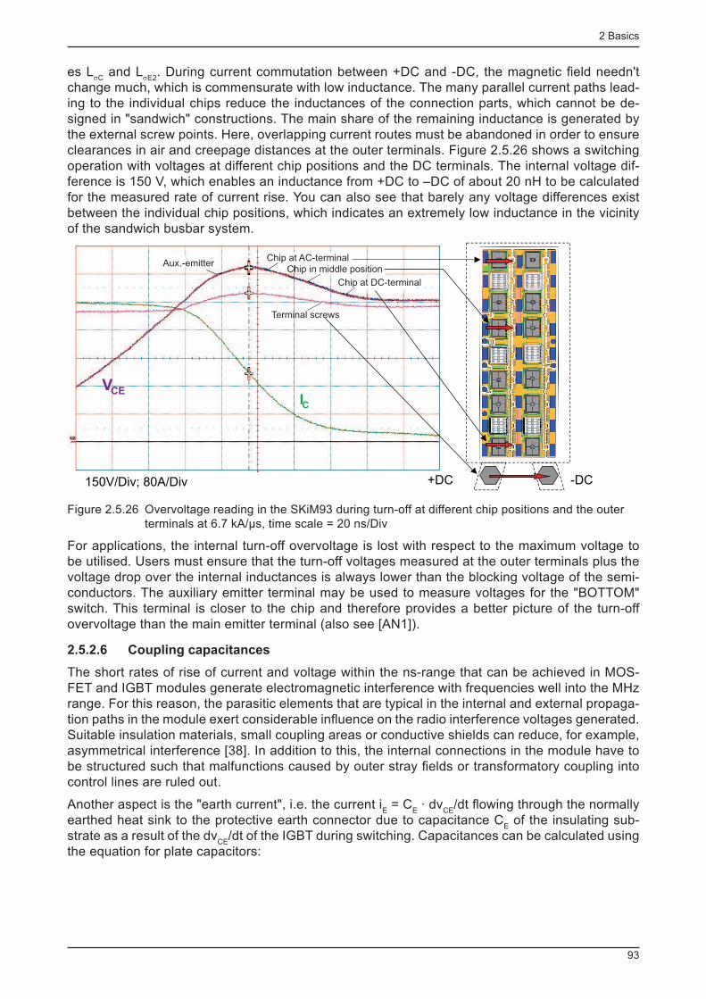
2 Basics
93
es L σ C
and L σ E2
. During current commutation between +DC and -DC, the magnetic fi eld needn't change much, which is commensurate with low inductance. The many parallel current paths lead-ing to the individual chips reduce the inductances of the connection parts, which cannot be de-signed in "sandwich" constructions. The main share of the remaining inductance is generated by the external screw points. Here, overlapping current routes must be abandoned in order to ensure clearances in air and creepage distances at the outer terminals. Figure 2.5.26 shows a switching operation with voltages at different chip positions and the DC terminals. The internal voltage dif-ference is 150 V, which enables an inductance from +DC to –DC of about 20 nH to be calculated for the measured rate of current rise. You can also see that barely any voltage differences exist between the individual chip positions, which indicates an extremely low inductance in the vicinity of the sandwich busbar system.
VCEIC
150V/Div; 80A/Div +DC -DC
Aux.-emitterChip at AC-terminal
Chip in middle position
Chip at DC-terminal
Terminal screws
Figure 2.5.26 Overvoltage reading in the SKiM93 during turn-off at different chip positions and the outer terminals at 6.7 kA/µs, time scale = 20 ns/Div
For applications, the internal turn-off overvoltage is lost with respect to the maximum voltage to be utilised. Users must ensure that the turn-off voltages measured at the outer terminals plus the voltage drop over the internal inductances is always lower than the blocking voltage of the semi-conductors. The auxiliary emitter terminal may be used to measure voltages for the "BOTTOM" switch. This terminal is closer to the chip and therefore provides a better picture of the turn-off overvoltage than the main emitter terminal (also see [AN1]).
2.5.2.6 Coupling capacitances
The short rates of rise of current and voltage within the ns-range that can be achieved in MOS-FET and IGBT modules generate electromagnetic interference with frequencies well into the MHz range. For this reason, the parasitic elements that are typical in the internal and external propaga-tion paths in the module exert considerable infl uence on the radio interference voltages generated. Suitable insulation materials, small coupling areas or conductive shields can reduce, for example, asymmetrical interference [38]. In addition to this, the internal connections in the module have to be structured such that malfunctions caused by outer stray fi elds or transformatory coupling into control lines are ruled out.
Another aspect is the "earth current", i.e. the current i E = C
E · dv
CE /dt fl owing through the normally
earthed heat sink to the protective earth connector due to capacitance C E of the insulating sub-
strate as a result of the dv CE
/dt of the IGBT during switching. Capacitances can be calculated using the equation for plate capacitors:

2 Basics
94
d
ACE
×e=
d (thickness) Al 2 O
3 : 0.38 mm or 0.63 mm; AlN: 0.63 mm;
ε = ε 0 ·ε
r =9.1·8.85e -12 F/m (Al
2 O
3 and AlN);
The following shares of substrate area can be estimated for a halfbridge module: - 40% "+DC" - 40% "AC" and - 15% "-DC"
The connection potential to earth and its amplitude when switched will depend on the earthing concept for the connected load. Suitable measures (e.g. Y-capacitors) must be taken to create a current path in the converter that closes a circuit close to the semiconductor; this must be done to ensure that current i
E does not fl ow through the controller and monitoring units. This earth current
would be identifi ed as a fault by a residual current protective device and may trigger this device. For installations where high leakage currents occur for functional reasons, special labelling re-quirements and mandatory minimum cross sections for the protective conductors exist (EN 50178, EN 61800-5-1).
Figure 2.5.27 compares the capacitances of the most common substrate materials in their stand-ard thicknesses. The deviating dielectric constants and the standard thicknesses depending on thermal conductivity (thickest substrate material being AlN with 630 µm, thinnest substrate re-quired in IMS structures, with 120 µm for epoxy insulation and 25 µm for polyimide insulation) result in different capacitances C
E and thus different limits for the maximum switching speed dv
CE /
dt for a maximum permissible earth current i E .
Capacity per unit area
0
20
40
60
80
100
120
140
Al O2 3 AlN Epoxy Polyimid
d=0.38 mmd=0.63 mm
d=0.12 mm
d=0.025 mm
[pF
/cm
]2
Figure 2.5.27 Capacitance per unit area for different insulating substrates
2.5.2.7 Circuit complexity
Optimal complexity cannot be defi ned in general. On the one hand, complex modules will re-duce equipment costs and minimise problems encountered when several components are to be combined in one circuit (parasitic inductances, interference, incorrect wiring). On the other hand, increasing complexity restricts module usability, rendering modules less general-purpose (think production quantities). Testing will become more extensive and the costs per module will increase. As the number of integrated components and connections increases, modules will be more likely to fail and the amount of circuitry that will have to be replaced in the event of faults will increase. Driver, sensor and protection assemblies in modules have to meet considerable requirements re-garding their thermal stability and electromagnetic compatibility.
Up to now, none of the following module confi gurations has gained acceptance as a "global stand-ard" with respect to driver integration. The general-purposeness of power modules is greatly im-paired by the integration of increasing driver functions; power modules are in fact becoming more and more like sub-systems. On the one hand, "intelligent" modules are aiming at real mass pro-duction markets (consumer, automotive); on the other hand, markets where many similar applica-

2 Basics
95
tions can be covered with innovative module systems consisting of similar basic units are also be-ing targeted. In the latter case, despite inevitable redundancies, users can still profi t from reduced system costs thanks to the synergies provided by module manufacturer.
Considering the arrangement of IGBT and diodes in the most commonly used power modules, the confi gurations shown in Figure 2.5.28 have managed to gain a strong footing, meeting the demands of most applications in power electronics and drive technology.
o)
a) b) c) d)
e) f) g) h)
i) j) k)
l) m)
n)
Figure 2.5.28 Important confi gurations for power modules with IGBT and diodes
2 Basics
96
To identify the circuit topologies shown in Figure 2.5.28, the SEMIKRON component designations contain the following letter combinations:a) GA: single switch, consisting of IGBT and hybrid inverse diode (for MOSFET modules here
and in the other confi gurations, mostly just a parasitic inverse diode). In case of external bridge circuits, the inverse diodes reciprocally act as freewheeling diodes.
b) GB: dual module (phase module, halfbridge module) consisting of two IGBT and hybrid diodes (freewheeling diodes)
c) GH: H-bridge with two arms consisting of IGBT and freewheeling diodesd) GAH: asymmetrical H-bridge with two diagonal IGBT with hybrid inverse diodes (freewheeling
diodes) and two freewheeling diodes across the other diagonale) GD: 3-phase bridge (sixpack, inverter) with three arms consisting of IGBT and freewheeling
diodesf) GAL: chopper module with IGBT, inverse diode and freewheeling diode on the collector sideg) GAR: chopper module with IGBT, inverse diode and freewheeling diode on the emitter sideh) GDL: 3-phase bridge "GD" with chopper "GAL" (brake chopper)i) B2U diode rectifi ers (to charge the DC link, semi-controlled B2H confi gurations with 2 thyris-
tors at the +DC are often used instead of pure diode bridges) and IGBT H-bridgej) B2U diode rectifi er and IGBT inverter (three-phase bridge)k) B6U diode rectifi er and IGBT chopper "GAL" (IGBT and freewheeling diode on the collector
side)l) B6U diode rectifi ers (to charge the DC link, semi-controlled B6H confi gurations with 3 thyris-
tors at the +DC are often used instead of pure diode bridges) and IGBT H-bridgem) B6U diode rectifi er and IGBT inverter (three-phase bridge)n) B6U diode rectifi er, IGBT chopper "GAL" and IGBT inverter (three-phase bridge)o) Phase module of a three-level inverter
2.5.2.8 Defi ned and safe failure behaviour in the event of module defects
In the event of module malfunction (e.g. caused by erroneous control signal), the total energy stored in the DC-link capacitors will be transferred, in a voltage-supplied circuit, for example, in the module case. Once the bond wires have melted, a large part of this energy is stored in the gener-ated plasma, which may cause the module to explode. In conventional transistor modules this may cause circuit interruption, short-circuit of the main terminals or even bridging of the insulation path. The resultant high kinetic energy could distribute plasma and particles of the module case across the module surroundings. Module case designs must limit the dangers involved where possible and ensure safe module rupture (e.g. by defi ned particle distribution).
There are developments in this fi eld that ensure, for example, that up to a defi ned energy level of 15 kJ, no particles will leave the module; even at 20 kJ the case might break, but no solid metal particles would be hurled into the surroundings [39]. IEC 60747-15 provides no defi nitions for a case rupture current or case rupture energy for power semiconductor modules.
2.5.2.9 Environmentally compatible recycling
Today’s power modules usually refrain from using toxic materials (e.g. BeO) and the number of materials used is kept as low as possible. Cases and other materials are fl ame-resistant and must not release toxic gas during burn-out (UL approval). In the recycling process, the module has to be dismantled and separated into metal and non-metal components. This must be easily achiev-able. For this reason, newer modules are cast solely using elastomeric materials (soft moulding). All semiconductor modules produced by SEMIKRON conform to RoHS.
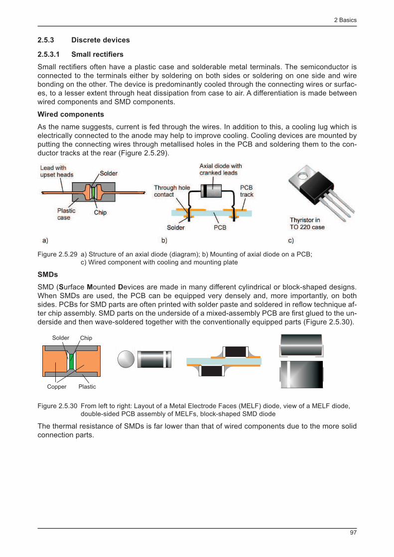
2 Basics
97
2.5.3 Discrete devices
2.5.3.1 Small rectifi ers
Small rectifi ers often have a plastic case and solderable metal terminals. The semiconductor is connected to the terminals either by soldering on both sides or soldering on one side and wire bonding on the other. The device is predominantly cooled through the connecting wires or surfac-es, to a lesser extent through heat dissipation from case to air. A differentiation is made between wired components and SMD components.
Wired components
As the name suggests, current is fed through the wires. In addition to this, a cooling lug which is electrically connected to the anode may help to improve cooling. Cooling devices are mounted by putting the connecting wires through metallised holes in the PCB and soldering them to the con-ductor tracks at the rear (Figure 2.5.29).
Figure 2.5.29 a) Structure of an axial diode (diagram); b) Mounting of axial diode on a PCB; c) Wired component with cooling and mounting plate
SMDs
SMD ( S urface M ounted D evices are made in many different cylindrical or block-shaped designs. When SMDs are used, the PCB can be equipped very densely and, more importantly, on both sides. PCBs for SMD parts are often printed with solder paste and soldered in refl ow technique af-ter chip assembly. SMD parts on the underside of a mixed-assembly PCB are fi rst glued to the un-derside and then wave-soldered together with the conventionally equipped parts (Figure 2.5.30).
ChipSolder
Copper Plastic
Figure 2.5.30 From left to right: Layout of a Metal Electrode Faces (MELF) diode, view of a MELF diode, double-sided PCB assembly of MELFs, block-shaped SMD diode
The thermal resistance of SMDs is far lower than that of wired components due to the more solid connection parts.
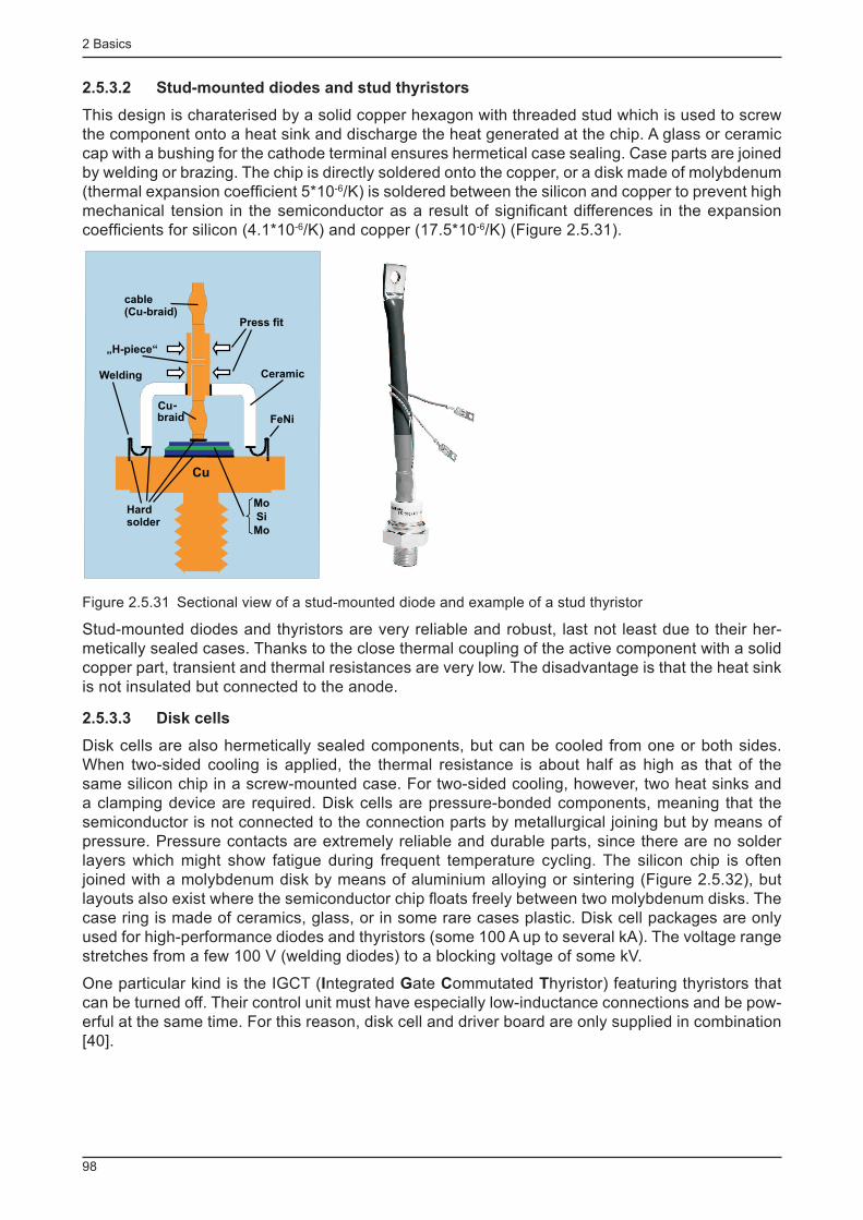
2 Basics
98
2.5.3.2 Stud-mounted diodes and stud thyristors
This design is charaterised by a solid copper hexagon with threaded stud which is used to screw the component onto a heat sink and discharge the heat generated at the chip. A glass or ceramic cap with a bushing for the cathode terminal ensures hermetical case sealing. Case parts are joined by welding or brazing. The chip is directly soldered onto the copper, or a disk made of molybdenum (thermal expansion coeffi cient 5*10 -6 /K) is soldered between the silicon and copper to prevent high mechanical tension in the semiconductor as a result of signifi cant differences in the expansion coeffi cients for silicon (4.1*10 -6 /K) and copper (17.5*10 -6 /K) (Figure 2.5.31).
Cu
FeNi
ßung Keramik
Quetschung
Cu -
Litze
„H -St ück “
Hartl ötungMo
Si
Mo
Kabel
(CuLitze)
Cu
FeNi
Welding Ceramic
Press fit
Cu-braid
„H-piece“
Hardsolder
Mo
Si
Mo
cable(Cu-braid)
Figure 2.5.31 Sectional view of a stud-mounted diode and example of a stud thyristor
Stud-mounted diodes and thyristors are very reliable and robust, last not least due to their her-metically sealed cases. Thanks to the close thermal coupling of the active component with a solid copper part, transient and thermal resistances are very low. The disadvantage is that the heat sink is not insulated but connected to the anode.
2.5.3.3 Disk cells
Disk cells are also hermetically sealed components, but can be cooled from one or both sides. When two-sided cooling is applied, the thermal resistance is about half as high as that of the same silicon chip in a screw-mounted case. For two-sided cooling, however, two heat sinks and a clamping device are required. Disk cells are pressure-bonded components, meaning that the semiconductor is not connected to the connection parts by metallurgical joining but by means of pressure. Pressure contacts are extremely reliable and durable parts, since there are no solder layers which might show fatigue during frequent temperature cycling. The silicon chip is often joined with a molybdenum disk by means of aluminium alloying or sintering (Figure 2.5.32), but layouts also exist where the semiconductor chip fl oats freely between two molybdenum disks. The case ring is made of ceramics, glass, or in some rare cases plastic. Disk cell packages are only used for high-performance diodes and thyristors (some 100 A up to several kA). The voltage range stretches from a few 100 V (welding diodes) to a blocking voltage of some kV.
One particular kind is the IGCT ( I ntegrated G ate C ommutated T hyristor) featuring thyristors that can be turned off. Their control unit must have especially low-inductance connections and be pow-erful at the same time. For this reason, disk cell and driver board are only supplied in combination [40].
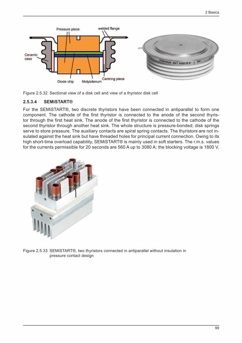
2 Basics
99
Figure 2.5.32 Sectional view of a disk cell and view of a thyristor disk cell
2.5.3.4 SEMiSTART®
For the SEMiSTART®, two discrete thyristors have been connected in antiparallel to form one component. The cathode of the fi rst thyristor is connected to the anode of the second thyris-tor through the fi rst heat sink. The anode of the fi rst thyristor is connected to the cathode of the second thyristor through another heat sink. The whole structure is pressure-bonded; disk springs serve to store pressure. The auxiliary contacts are spiral spring contacts. The thyristors are not in-sulated against the heat sink but have threaded holes for principal current connection. Owing to its high short-time overload capability, SEMiSTART® is mainly used in soft starters. The r.m.s. values for the currents permissible for 20 seconds are 560 A up to 3080 A; the blocking voltage is 1800 V.
Figure 2.5.33 SEMiSTART®, two thyristors connected in antiparallel without insulation in pressure contact design
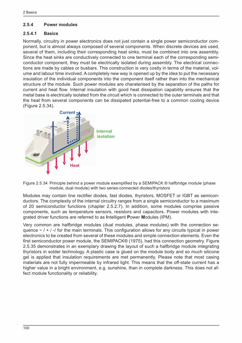
2 Basics
100
2.5.4 Power modules
2.5.4.1 Basics
Normally, circuitry in power electronics does not just contain a single power semiconductor com-ponent, but is almost always composed of several components. When discrete devices are used, several of them, including their corresponding heat sinks, must be combined into one assembly. Since the heat sinks are conductively connected to one terminal each of the corresponding semi-conductor component, they must be electrically isolated during assembly. The electrical connec-tions are made by cables or busbars. This construction is very costly in terms of the material, vol-ume and labour time involved. A completely new way is opened up by the idea to put the necessary insulation of the individual components into the component itself rather than into the mechanical structure of the module. Such power modules are charaterised by the separation of the paths for current and heat fl ow. Internal insulation with good heat dissipation capability ensures that the metal base is electrically isolated from the circuit which is connected to the outer terminals and that the heat from several components can be dissipated potential-free to a common cooling device (Figure 2.5.34).
Heat
Internal
isolation
Current
Figure 2.5.34 Principle behind a power module exemplifi ed by a SEMIPACK ® halfbridge module (phase module, dual module) with two series-connected diodes/thyristors
Modules may contain line rectifi er diodes, fast diodes, thyristors, MOSFET or IGBT as semicon-ductors. The complexity of the internal circuitry ranges from a single semiconductor to a maximum of 20 semiconductor functions (chapter 2.5.2.7). In addition, some modules comprise passive components, such as temperature sensors, resistors and capacitors. Power modules with inte-grated driver functions are referred to as I ntelligent P ower M odules (IPM).
Very common are halfbridge modules (dual modules, phase modules) with the connection se-quence ~ / + / -/ for the main terminals. This confi guration allows for any circuits typical in power electronics to be created from several of these modules and simple connection elements. Even the fi rst semiconductor power module, the SEMIPACK® (1975), had this connection geometry. Figure 2.5.35 demonstrates in an exemplary drawing the layout of such a halfbridge module integrating thyristors in solder technology. A plastic case is glued on the module body and so much silicone gel is applied that insulation requirements are met permanently. Please note that most casing materials are not fully impermeable by infrared light. This means that the off-state current has a higher value in a bright environment, e.g. sunshine, than in complete darkness. This does not af-fect module functionality or reliability.
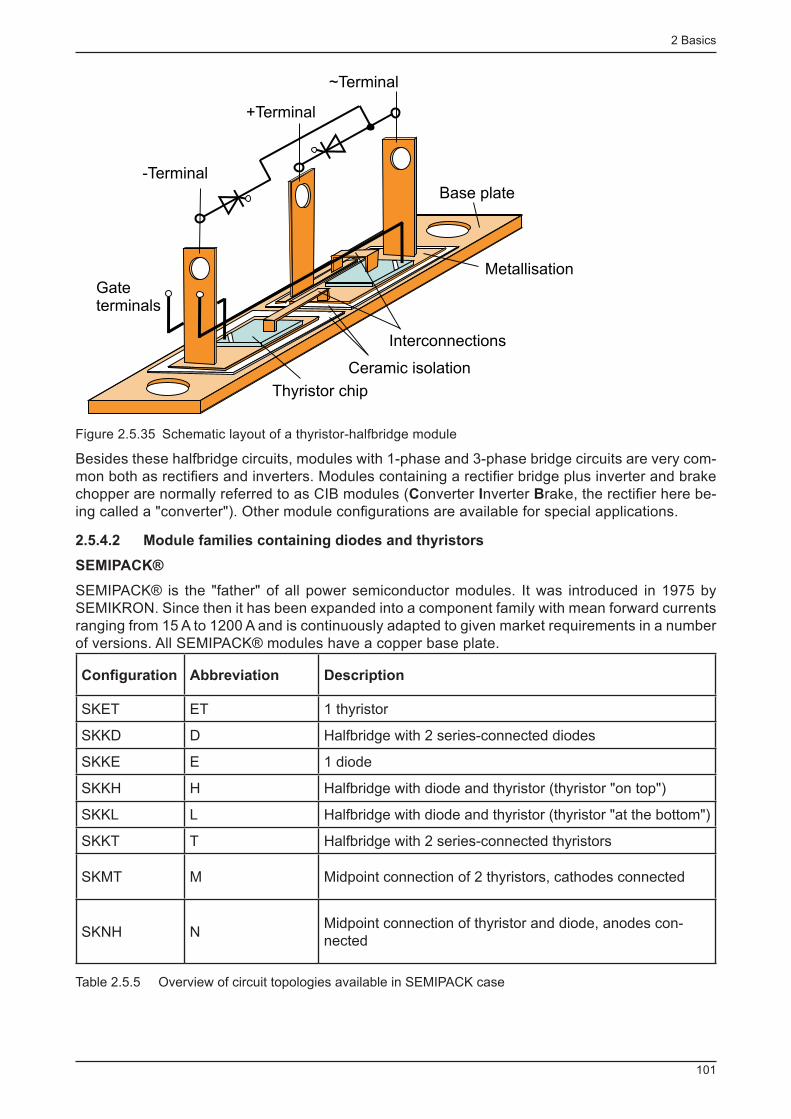
2 Basics
101
Metallisation
Gateterminals
Base plate
Thyristor chip
Interconnections
Ceramic isolation
-Terminal
+Terminal
~Terminal
Figure 2.5.35 Schematic layout of a thyristor-halfbridge module
Besides these halfbridge circuits, modules with 1-phase and 3-phase bridge circuits are very com-mon both as rectifi ers and inverters. Modules containing a rectifi er bridge plus inverter and brake chopper are normally referred to as CIB modules ( C onverter I nverter B rake, the rectifi er here be-ing called a "converter"). Other module confi gurations are available for special applications.
2.5.4.2 Module families containing diodes and thyristors
SEMIPACK®
SEMIPACK® is the "father" of all power semiconductor modules. It was introduced in 1975 by SEMIKRON. Since then it has been expanded into a component family with mean forward currents ranging from 15 A to 1200 A and is continuously adapted to given market requirements in a number of versions. All SEMIPACK® modules have a copper base plate.
Confi guration Abbreviation Description
SKET ET 1 thyristor
SKKD D Halfbridge with 2 series-connected diodes
SKKE E 1 diode
SKKH H Halfbridge with diode and thyristor (thyristor "on top")
SKKL L Halfbridge with diode and thyristor (thyristor "at the bottom")
SKKT T Halfbridge with 2 series-connected thyristors
SKMT M Midpoint connection of 2 thyristors, cathodes connected
SKNH N Midpoint connection of thyristor and diode, anodes con-nected
Table 2.5.5 Overview of circuit topologies available in SEMIPACK case

2 Basics
102
SE
MIP
AC
K®
Me
an
fo
rwa
rd
cu
rre
nt
Re
ve
rse
vo
lta
ge
Co
nfi
gu
rati
on
s
Te
ch
no
log
y
Ma
in c
urr
en
t
term
ina
ls
SEMIPACK®0 15 A 600 V –1600 V
D, E, H, T Chips soldered on both sides Plug
SEMIPACK®1 28 A –119 A
800 V–2200 V
D, E, H, L, T, M, N
Chips soldered on both sides Screws
SEMIPACK®2 122 A –212 A
800 V–2200 V
D, E, H, T Chips soldered on both sides Screws
SEMIPACK®3 250 A –380 A
800 V–2200 V
D, E, H, T Chips, soldered / bonded or with pressure contacts
Screws
SEMIPACK®4 330 A–600 A
800 V–2200 V
E, ET Chip, pressure contact Screws
SEMIPACK®5 570 A–701 A
800 V–2200 V
D, H, T Chips, pressure contact Screws
SEMIPACK®6 740 A–1180 A
1400 V–2200 V
E, ET Chip, pressure contact Screws
Table 2.5.6 Overview of SEMIPACK case names and connection technology
Figure 2.5.36 a) SEMIPACK®1 (soldered chips, soldered / bonded top side, aux. spring contacts) b) SEMIPACK®5 (pressure-contact chips)
SEMIPACK®fast
This name is used for fast diodes available in D, E, M and N confi gurations in the case types SEMI-PACK®1 and 2, or SEMITRANS®4. Blocking voltages range from 200 V to 1700 V.

2 Basics
103
SEMIPONT®
Single-phase and three-phase rectifi er modules with a DC output current from 2 A to 210 A and blocking voltages from 200 V to 1800 V form the SEMIPONT® family. In addition to pure diode bridges for uncontrolled rectifying, semi-controlled and fully controlled thyristor bridges with/with-out brake chopper or freewheeling diode are also available. 3 antiparallel thyristor pairs in one case can be used to form AC switches (W3C circuits).
Depending on the amperage, modules are available in many case types with plug-in, solder or screw connections. Some designs have copper base plates. Especially in the lower power range, the chips are soldered onto a DBC ceramic substrate which is pressed on the heat sink by the case and the fastening screw(s).
Figure 2.5.37 Examples of SEMIPONT ® designs
SEMITOP®
This module family comprising 4 case sizes does not feature a copper base plate. Just one screw is needed to press the module on the heat sink. Current and control terminals feature solder pin connections. Apart from circuits with IGBT (chapter 2.5.4.3)), a number of confi gurations are avail-able that incorporate diodes and thyristors, e.g. single-phase and three-phase uncontrolled, semi-controlled and fully controlled bridges, single-phase, two-phase and three-phase AC switches and many other variants. With blocking voltages from 600 V to 1600 V, the r.m.s. currents or the DC mean values lie between 25 A and 210 A.
Figure 2.5.38 SEMITOP®1, semi-transparent case (a) and SEMITOP®4 as semi-controlled three-phase bridge with brake chopper (b)
SEMiX®
These modules with copper base plate, which are designed for higher power output, come with halfbridges and three-phase bridges with diode and thyristor circuits. With a module height of 17 mm, they are mainly intended for use with SEMiX® IGBT modules. With a blocking voltage of 1200 V or 1600 V, the current densities lie between 170 A and 340 A. What should be pointed out here is the very easy mounting of PCBs used to drive the thyristor above the module by way of spring contacts.
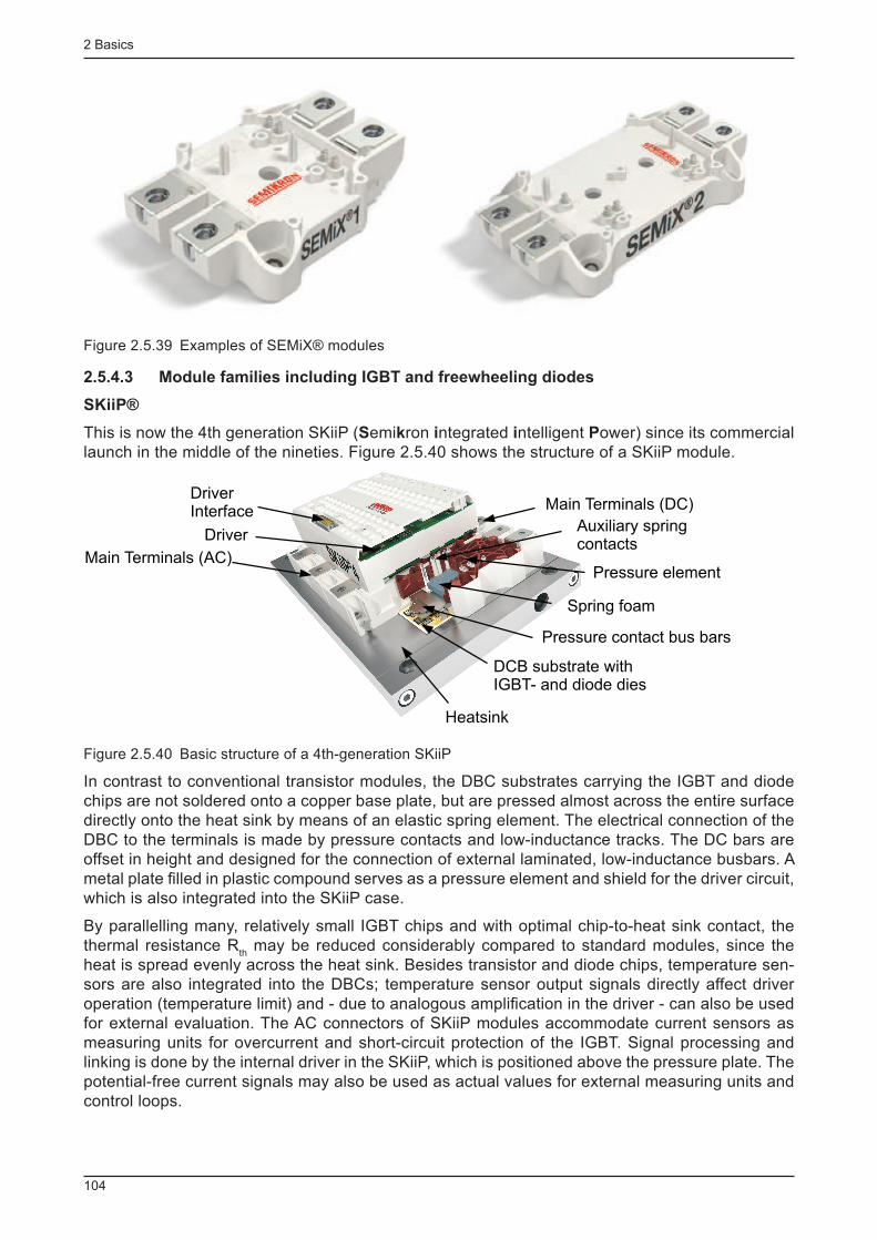
2 Basics
104
Figure 2.5.39 Examples of SEMiX® modules
2.5.4.3 Module families including IGBT and freewheeling diodes
SKiiP®
This is now the 4th generation SKiiP ( S emi k ron i ntegrated i ntelligent P ower) since its commercial launch in the middle of the nineties. Figure 2.5.40 shows the structure of a SKiiP module.
Heatsink
Pressure contact bus bars
DCB substrate withIGBT- and diode dies
Spring foam
Pressure element
DriverAuxiliary springcontacts
DriverInterface
Main Terminals (AC)
Main Terminals (DC)
Figure 2.5.40 Basic structure of a 4th-generation SKiiP
In contrast to conventional transistor modules, the DBC substrates carrying the IGBT and diode chips are not soldered onto a copper base plate, but are pressed almost across the entire surface directly onto the heat sink by means of an elastic spring element. The electrical connection of the DBC to the terminals is made by pressure contacts and low-inductance tracks. The DC bars are offset in height and designed for the connection of external laminated, low-inductance busbars. A metal plate fi lled in plastic compound serves as a pressure element and shield for the driver circuit, which is also integrated into the SKiiP case.
By parallelling many, relatively small IGBT chips and with optimal chip-to-heat sink contact, the thermal resistance R
th may be reduced considerably compared to standard modules, since the
heat is spread evenly across the heat sink. Besides transistor and diode chips, temperature sen-sors are also integrated into the DBCs; temperature sensor output signals directly affect driver operation (temperature limit) and - due to analogous amplifi cation in the driver - can also be used for external evaluation. The AC connectors of SKiiP modules accommodate current sensors as measuring units for overcurrent and short-circuit protection of the IGBT. Signal processing and linking is done by the internal driver in the SKiiP, which is positioned above the pressure plate. The potential-free current signals may also be used as actual values for external measuring units and control loops.

2 Basics
105
Four case sizes (2, 3, 4 and 6 IGBT halfbridges) and their matching driver components can be used to build H-bridges or three-phase bridges in 1200 V and 1700 V technology with the aid of simple external connections, for example. Converter performance without external parallel con-nection covers a range of 100 kW up to 1.5 MW.
Advantages of SKiiPs over conventional modules are, for example: - About twice the temperature cycling capability in long-term use - Reduced thermal resistance by direct heat transfer between chip, DBC and heat sink - Very compact designs with high power density - Low switching overvoltages due to consistent low-inductance structure, i.e. high permissible DC-link voltage and reduced interference
- Optimal matching of the intelligent driver integrated in SKiiP - Pre-assembly of power modules on heat sink, optimum thermal paste application in screen print-ing process
- Low-inductance converter design by way of parallel current paths (4x 600 A halfbridge modules rather than 2x 2400 A single switches)
- Manufacturer-side load testing on complete systems.
In Table 2.5.7 3rd and 4th generation SKiiP cases are listed. Besides the heat sink shown below, SKiiPs may also be mounted on other air or water-cooled heat sinks.
SKiiP3 1200 V / 1700 V
Halfbridges 2 3 4
I C
1000 A 1500 A 2000 A
SKiiP4 1200 A / 1700 V
Parallel IGBT halfbridges
3 4 6
I C@TS=25°C
1800 A 2400 A 3600 A
Table 2.5.7 Case designs for 3rd and 4th generation SKiiPs
SKiM
SKiM modules have no base plate and are designed for the medium power range between SKiiP and MiniSKiiP applications. This module features SKiiP technology throughout. SKiM63/93 is the fi rst IGBT module to contain no solder whatsoever. The elimination of all solder connections re-sults in 5 times the thermal cycling capability compared to standard soldered modules with base plate. Thanks to its compactness, this module, which was originally developed and qualifi ed for the automotive industry, is also an interesting solution for standard drives in the power range from 30 kW to 150 kW. The main terminals are located at the front ends, leaving plenty of space for the driver board on top. It is mounted without solder by means of spring contacts.

2 Basics
106
Pressure contactbus bars
DCB substrate withsintered IGBT and diode
Spring foam
Pressureelement
Auxiliary springcontacts
Main terminals (DC)
Figure 2.5.41 Cross section of a SKiM63 module
Like its predecessors, SKiM4 and SKiM5, this module contains a three-phase bridge circuit (GD, 6-pack). Non-standard versions as choppers (3-phase GAL/GAR for asymmetrical H-bridges, e.g. for reluctance motor applications) or as phase modules for three-level inverters ( M ulti L evel I n-verter, MLI) also exist. SKiM is available in the voltage classes 600 V, 1200 V and 1700 V.
SEMITRANS®
SEMITRANS is the name for transistor module cases whose most important types have been standardised in case widths of 34 mm and 61 mm in accordance with IEC 60191-2. These mod-ules feature a copper base plate whose main terminals are designed as exterior screw contacts (exception: SEMITRANS 6). Owing to the centre position of the DC terminals, which are highly symmetrical in relation to chip connection (very good current distribution between parallel chips), these modules are especially low-ohmic and low-inductive compared to the 17-mm-high modules with load terminals at the front ends (SEMiX). Auxiliary terminals are mostly designed as "fast-on" plug-in contacts (exception: SEMITRANS 4). Apart from a few MOSFET modules, IGBT and soft recovery diodes are used in the voltage classes 600 V, 1200 V and 1700 V. These modules are part of the medium power range with current classes ranging from 20 A (GD, 6-pack) to 800 A (GA, single switch).
SEMITRANS M1
SEMITRANS 2 (34 mm)
SEMITRANS 3 (61 mm)
SEMITRANS 4 (61 mm)
SEMITRANS 5
SEMITRANS 6
Figure 2.5.42 Case designs in the SEMITRANS family
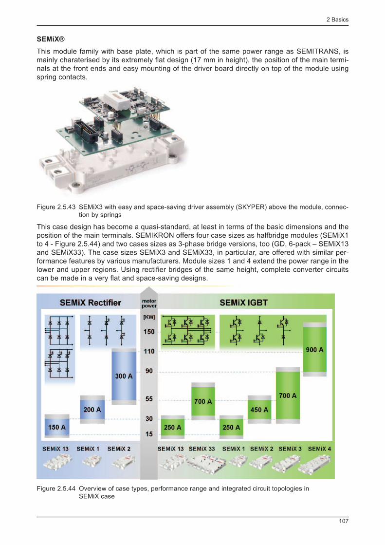
2 Basics
107
SEMiX®
This module family with base plate, which is part of the same power range as SEMITRANS, is mainly charaterised by its extremely fl at design (17 mm in height), the position of the main termi-nals at the front ends and easy mounting of the driver board directly on top of the module using spring contacts.
Figure 2.5.43 SEMiX3 with easy and space-saving driver assembly (SKYPER) above the module, connec-tion by springs
This case design has become a quasi-standard, at least in terms of the basic dimensions and the position of the main terminals. SEMIKRON offers four case sizes as halfbridge modules (SEMiX1 to 4 - Figure 2.5.44) and two cases sizes as 3-phase bridge versions, too (GD, 6-pack – SEMiX13 and SEMiX33). The case sizes SEMiX3 and SEMiX33, in particular, are offered with similar per-formance features by various manufacturers. Module sizes 1 and 4 extend the power range in the lower and upper regions. Using rectifi er bridges of the same height, complete converter circuits can be made in a very fl at and space-saving designs.
Figure 2.5.44 Overview of case types, performance range and integrated circuit topologies in SEMiX case

2 Basics
108
The internal structure of a SEMiX module is shown in Figure 2.5.45. Depending on the module size, identical DBC substrates are connected in parallel. Each DBC substrate contains a pair of IGBT and the corresponding inverse diodes. SEMiX modules come in the conventional module design with copper base plate, soldered ceramic substrates, soldered and bonded chips and sol-dered terminals and intermediate links. Non-standard here are spring contacts for the auxiliary terminals and the integrated temperature sensor (NTC).
- DCTerminal
+ DCTerminal
IGBT Diode Interconnectionbetween DBCsubstrates
Temperaturesensor
~ ACTerminals
3x paralled DBC substrates with IGBT anddiode chips in half-bridge configuration
Figure 2.5.45 Internal structure of a SEMiX3 module
MiniSKiiP
Pressure-contact MiniSKiiP are IGBT modules in SKiiP technology for the lower power range, boasting fl exibility and easy assembly. The basic structure of this module is shown in Figure 2.5.46.
Heatsink
Ceramic substrate DCB
Chip
Bond wire
Contact spring
Case
Preasure top with screw
Printed circuit board PCB
Figure 2.5.46 MiniSKiiP layout
MiniSKiiPs are composed of: - DBC insulation substrate with soldered and wire-bonded semiconductor chips (e.g. IGBT, MOS-FET, diodes, thyristors) and other components such as current and temperature sensors
- the silicone fi lled case with integrated contact springs and glue-bonded DBC - hard plastic cover with pressure plate
One or two screws are used for the entire electrical and thermal connections (to the heat sink), making a detachable, friction-locked connection between SKiiP cover, PCB, MiniSKiiP and heat sink. The contact springs have several functions: they make the electrical connection between the power semiconductor circuit on the DBC and the other circuits on the base PCB, and also serve as pressure spring pad for pressing the DCB onto the heat sink in the mounted state.

2 Basics
109
The large number of springs spread over the entire MiniSKiiP surface ensures even pressure be-tween component and heat sink, which ensures a low thermal contact resistance. For the current range above 20 A, the contacts are connected in parallel. The multitude of spring shafts results in a high degree of fl exibility concerning the creation of many different circuits for drives and power supply systems, as well as other applications. Four case sizes designed for different power ranges are available in the 2nd generation, ranging from MiniSKiiP 0 (600 V IGBT, rated current up to 20 A) to MiniSKiiP 3 (600 V and 1200 V IGBT, rated currents up to 150 A).
Figure 2.5.47 Standard MiniSKiiP designs (dimensions in mm) and circuits
SEMITOP
The aforementioned SEMITOP module series comes in 4 case sizes (Figure 2.5.38). Like the SKiiP, SKiM and MiniSKiiP, SEMITOP also belongs to those modules without copper base plate that generate large-surface pressure across the DBC-to-heat sink connection using a special type of plastic case. A single screw makes a friction-locked connection between module and heat sink. Unlike in MiniSKiiP, contact with the PCB is made by solderable pin connectors.

2 Basics
110
Since a maximum of 12 power components can be integrated in such a small module, SEMITOP modules are preferred in low-power applications with low space requirements. The space between the solder pins can be fully utilised to accommodate other PCB components.
2.6 Integration of sensors, protective equipment and
driver electronics
A few examples of the integration of peripheral functions in power modules are described below. These are arranged in order of degree of integration.
2.6.1 Modules with integrated current measurement
Firstly, current measurements in modules are taken to protect the power semiconductors from overcurrent, and secondly, the current signal is also required for current control loops. Rough monitoring is suffi cient for the fi rst task, which is why the semiconductor itself can be utilised as a current sensor (V
CE(sat) monitoring). The latter must be very accurate (2%…5%), very dynamic
(response times ~ 1 µs) and requires a frequency range from DC to some 10 kHz.
Current shunts
Current shunts for taking direct measurements are integrated into the emitter path (-DC) of IGBT modules or placed at the AC output. The three square components in Figure 2.6.1 show a solution for current measurement in the emitter path of three low-side IGBT in a three-phase inverter mod-ule. Evaluation must be performed using a differential amplifi er in the driver electronics stage. The connecting pads at the sides ensure low-inductance coupling with the main current path.
The problem with the use of shunts is the discrepancy between the low measurable voltage range in a disturbed environment and the losses in the shunt. A 5 mΩ shunt has a voltage drop of just 100 mV at 20 A, but 2 W losses. With such a power loss, the limits for PCB assembly have been reached. Shunts that are integrated in the DBC provide the advantage that the heat loss can be directly dissipated through the heat sink. This extends the usable current range on the PCB from approx. 20 A to approx. 50 A. The disadvantage here is that "precious" DBC space is lost.
Figure 2.6.1 Current shunts (made by Isabellenhütte) in the emitter path of a MiniSKiiP IGBT module
Current sensors
For currents above 50 A, electrically insulated transmitters operating according to various princi-ples are used (transformer, Hall effect, magneto-resistive effect). SKiiP uses compensating trans-ducers (Figure 2.6.2), which are charaterised by high precision, a wide frequency range and a high overload capability. Sensor evaluation is part of the IPM electronics and the protection concept. In the principle presented here, the magnetic fi eld of the main current is measured in an air gap of the transmitter core and, with the aid of an amplifi er, a current is impressed on an auxiliary winding which compensates the magnetic fi eld to zero. The compensation current is a direct map of the main current. It is possible to measure DC current and detect the direction of current fl ow.
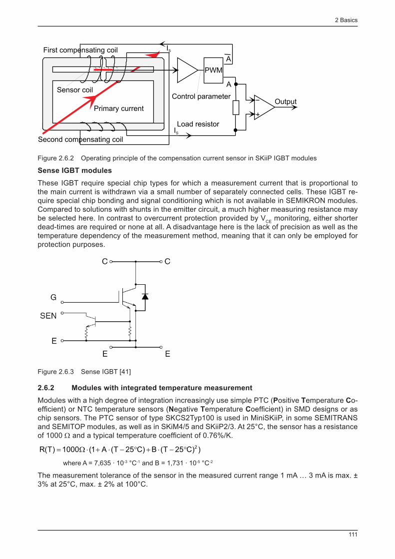
2 Basics
111
First compensating coil
Second compensating coil
Sensor coil
Primary currentOutput
Load resistorIS
PWM
A
A
Control parameter
IS
Figure 2.6.2 Operating principle of the compensation current sensor in SKiiP IGBT modules
Sense IGBT modules
These IGBT require special chip types for which a measurement current that is proportional to the main current is withdrawn via a small number of separately connected cells. These IGBT re-quire special chip bonding and signal conditioning which is not available in SEMIKRON modules. Compared to solutions with shunts in the emitter circuit, a much higher measuring resistance may be selected here. In contrast to overcurrent protection provided by V
CE monitoring, either shorter
dead-times are required or none at all. A disadvantage here is the lack of precision as well as the temperature dependency of the measurement method, meaning that it can only be employed for protection purposes.
Figure 2.6.3 Sense IGBT [41]
2.6.2 Modules with integrated temperature measurement
Modules with a high degree of integration increasingly use simple PTC ( P ositive T emperature C o-effi cient) or NTC temperature sensors ( N egative T emperature C oeffi cient) in SMD designs or as chip sensors. The PTC sensor of type SKCS2Typ100 is used in MiniSKiiP, in some SEMITRANS and SEMITOP modules, as well as in SKiM4/5 and SKiiP2/3. At 25°C, the sensor has a resistance of 1000 Ω and a typical temperature coeffi cient of 0.76%/K.
))C25T(B)C25T(A1(1000)T(R 2°-×+°-×+×W=
where A = 7,635 · 10 -3 °C -1 and B = 1,731 · 10 -5 °C -2
The measurement tolerance of the sensor in the measured current range 1 mA … 3 mA is max. ± 3% at 25°C, max. ± 2% at 100°C.
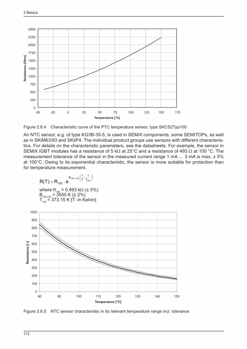
2 Basics
112
0
250
500
750
1000
1250
1500
1750
2000
2250
2500
-50 -25 0 25 50 75 100 125 150 175
Temperature [°C]
Resis
tan
ce
[Oh
m]
Figure 2.6.4 Characteristic curve of the PTC temperature sensor, type SKCS2Typ100
An NTC sensor, e.g. of type KG3B-35-5, is used in SEMiX components, some SEMITOPs, as well as in SKiM63/93 and SKiiP4. The individual product groups use sensors with different characteris-tics. For details on the characteristic parameters, see the datasheets. For example, the sensor in SEMiX IGBT modules has a resistance of 5 kΩ at 25°C and a resistance of 493 Ω at 100 °C. The measurement tolerance of the sensor in the measured current range 1 mA … 3 mA is max. ± 5% at 100°C. Owing to its exponential characteristic, the sensor is more suitable for protection than for temperature measurement.
÷÷ø
öççè
æ-×
×= 100125/100
T
1
T
1B
100 eR)T(R
where R 100
= 0.493 kΩ (± 5%) B
100/125 = 3550 K (± 2%)
T 100
= 373.15 K [T -in Kelvin]
0
100
200
300
400
500
600
700
800
900
1000
80 90 100 110 120 130 140 150
Temperature [°C]
Re
sis
tan
ce
[]
W
Figure 2.6.5 NTC sensor characteristic in its relevant temperature range incl. tolerance
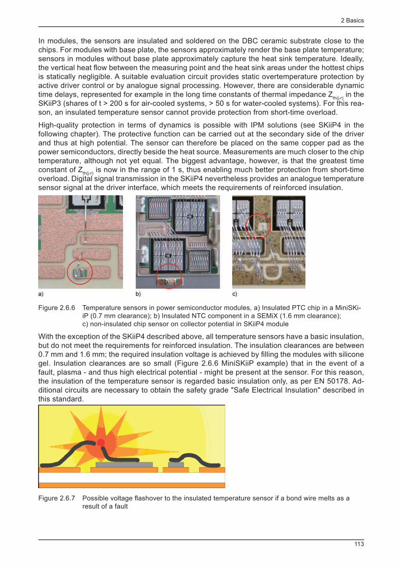
2 Basics
113
In modules, the sensors are insulated and soldered on the DBC ceramic substrate close to the chips. For modules with base plate, the sensors approximately render the base plate temperature; sensors in modules without base plate approximately capture the heat sink temperature. Ideally, the vertical heat fl ow between the measuring point and the heat sink areas under the hottest chips is statically negligible. A suitable evaluation circuit provides static overtemperature protection by active driver control or by analogue signal processing. However, there are considerable dynamic time delays, represented for example in the long time constants of thermal impedance Z
th(j-r) in the
SKiiP3 (shares of t > 200 s for air-cooled systems, > 50 s for water-cooled systems). For this rea-son, an insulated temperature sensor cannot provide protection from short-time overload.
High-quality protection in terms of dynamics is possible with IPM solutions (see SKiiP4 in the following chapter). The protective function can be carried out at the secondary side of the driver and thus at high potential. The sensor can therefore be placed on the same copper pad as the power semiconductors, directly beside the heat source. Measurements are much closer to the chip temperature, although not yet equal. The biggest advantage, however, is that the greatest time constant of Z
th(j-r) is now in the range of 1 s, thus enabling much better protection from short-time
overload. Digital signal transmission in the SKiiP4 nevertheless provides an analogue temperature sensor signal at the driver interface, which meets the requirements of reinforced insulation.
Figure 2.6.6 Temperature sensors in power semiconductor modules, a) Insulated PTC chip in a MiniSKi-iP (0.7 mm clearance); b) Insulated NTC component in a SEMiX (1.6 mm clearance); c) non-insulated chip sensor on collector potential in SKiiP4 module
With the exception of the SKiiP4 described above, all temperature sensors have a basic insulation, but do not meet the requirements for reinforced insulation. The insulation clearances are between 0.7 mm and 1.6 mm; the required insulation voltage is achieved by fi lling the modules with silicone gel. Insulation clearances are so small (Figure 2.6.6 MiniSKiiP example) that in the event of a fault, plasma - and thus high electrical potential - might be present at the sensor. For this reason, the insulation of the temperature sensor is regarded basic insulation only, as per EN 50178. Ad-ditional circuits are necessary to obtain the safety grade "Safe Electrical Insulation" described in this standard.
Figure 2.6.7 Possible voltage fl ashover to the insulated temperature sensor if a bond wire melts as a result of a fault
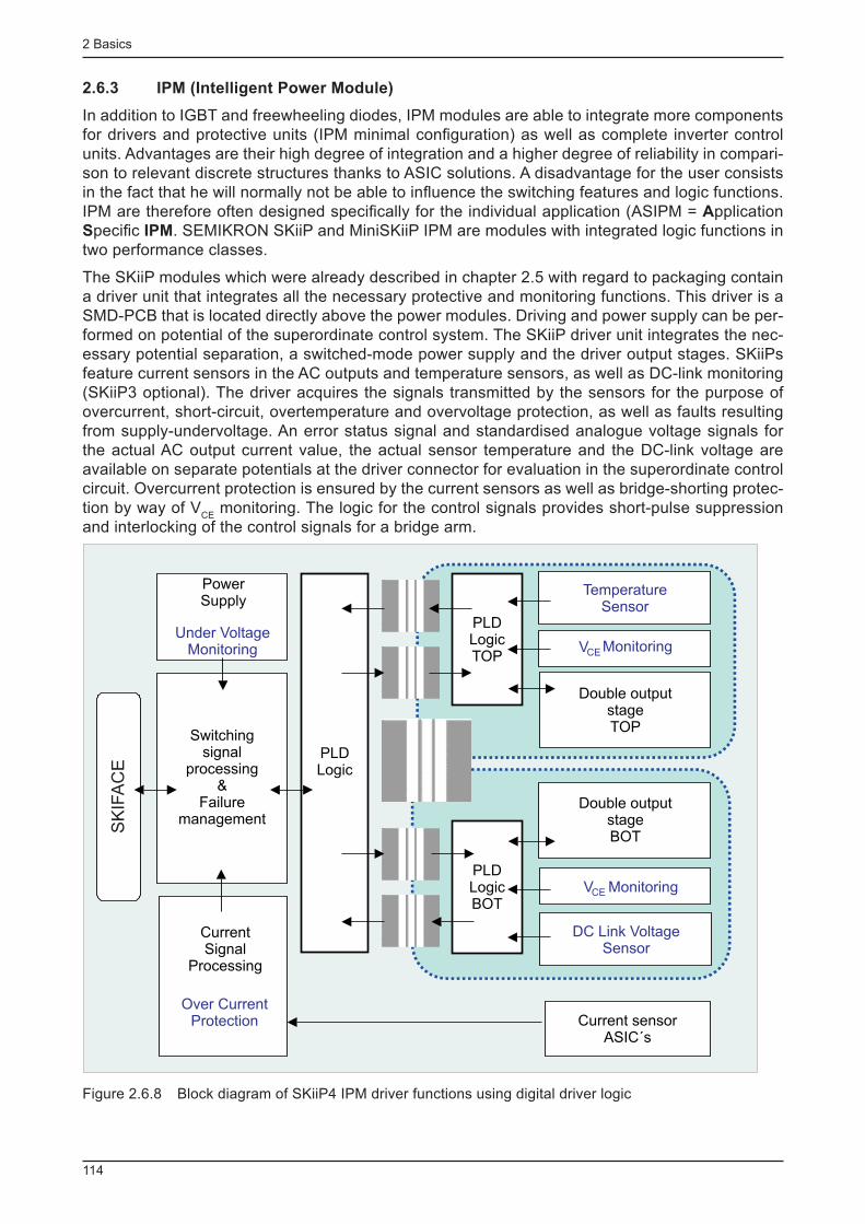
2 Basics
114
2.6.3 IPM (Intelligent Power Module)
In addition to IGBT and freewheeling diodes, IPM modules are able to integrate more components for drivers and protective units (IPM minimal confi guration) as well as complete inverter control units. Advantages are their high degree of integration and a higher degree of reliability in compari-son to relevant discrete structures thanks to ASIC solutions. A disadvantage for the user consists in the fact that he will normally not be able to infl uence the switching features and logic functions. IPM are therefore often designed specifi cally for the individual application (ASIPM = A pplication S pecifi c IPM . SEMIKRON SKiiP and MiniSKiiP IPM are modules with integrated logic functions in two performance classes.
The SKiiP modules which were already described in chapter 2.5 with regard to packaging contain a driver unit that integrates all the necessary protective and monitoring functions. This driver is a SMD-PCB that is located directly above the power modules. Driving and power supply can be per-formed on potential of the superordinate control system. The SKiiP driver unit integrates the nec-essary potential separation, a switched-mode power supply and the driver output stages. SKiiPs feature current sensors in the AC outputs and temperature sensors, as well as DC-link monitoring (SKiiP3 optional). The driver acquires the signals transmitted by the sensors for the purpose of overcurrent, short-circuit, overtemperature and overvoltage protection, as well as faults resulting from supply-undervoltage. An error status signal and standardised analogue voltage signals for the actual AC output current value, the actual sensor temperature and the DC-link voltage are available on separate potentials at the driver connector for evaluation in the superordinate control circuit. Overcurrent protection is ensured by the current sensors as well as bridge-shorting protec-tion by way of V
CE monitoring. The logic for the control signals provides short-pulse suppression
and interlocking of the control signals for a bridge arm.
VCEMonitoring
DC Link Voltage
Sensor
Double outputstage
TOP
PLD
Logic
TOP
PLD
Logic
BOT
Double output
stage
BOT
VCEMonitoring
Temperature
Sensor
Current sensor
ASIC‘s
PLD
Logic
Power
Supply
Under Voltage
Monitoring
SK
IFA
CE
Current
Signalprocessing
Over Current
Protection
Switching
signal
processing
&
Failure
management
VCE Monitoring
DC Link VoltageSensor
Double outputstageTOP
PLDLogicTOP
PLDLogicBOT
VCE Monitoring
TemperatureSensor
Current sensorASIC´s
PLDLogic
PowerSupply
Under VoltageMonitoring
CurrentSignal
Processing
Over CurrentProtection
Switchingsignal
processing&
Failuremanagement
Double outputstageBOT
SK
IFA
CE
Figure 2.6.8 Block diagram of SKiiP4 IPM driver functions using digital driver logic
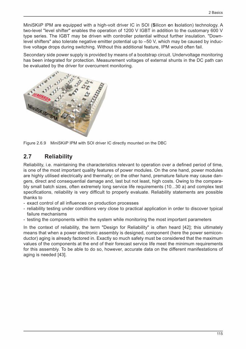
2 Basics
115
MiniSKiiP IPM are equipped with a high-volt driver IC in SOI ( S ilicon o n I solation) technology. A two-level "level shifter" enables the operation of 1200 V IGBT in addition to the customary 600 V type series. The IGBT may be driven with controller potential without further insulation. "Down-level shifters" also tolerate negative emitter potential up to –50 V, which may be caused by induc-tive voltage drops during switching. Without this additional feature, IPM would often fail.
Secondary side power supply is provided by means of a bootstrap circuit. Undervoltage monitoring has been integrated for protection. Measurement voltages of external shunts in the DC path can be evaluated by the driver for overcurrent monitoring.
Figure 2.6.9 MiniSKiiP IPM with SOI driver IC directly mounted on the DBC
2.7 Reliability
Reliability, i.e. maintaining the characteristics relevant to operation over a defi ned period of time, is one of the most important quality features of power modules. On the one hand, power modules are highly utilised electrically and thermally; on the other hand, premature failure may cause dan-gers, direct and consequential damage and, last but not least, high costs. Owing to the compara-bly small batch sizes, often extremely long service life requirements (10...30 a) and complex test specifi cations, reliability is very diffi cult to properly evaluate. Reliability statements are possible thanks to - exact control of all infl uences on production processes - reliability testing under conditions very close to practical application in order to discover typical failure mechanisms
- testing the components within the system while monitoring the most important parameters
In the context of reliability, the term "Design for Reliability" is often heard [42]; this ultimately means that when a power electronic assembly is designed, component (here the power semicon-ductor) aging is already factored in. Exactly so much safety must be considered that the maximum values of the components at the end of their forecast service life meet the minimum requirements for this assembly. To be able to do so, however, accurate data on the different manifestations of aging is needed [43].

2 Basics
116
Safety margin at the beginning
Minimum application requirements
Parameter change by aging
End of life
t
Maximumparameter variation
Figure 2.7.1 Design process for reliability. Target: to suffi ciently factor in safety and reliability at the beginning of the service life to ensure that product requirements are still met at the end of service life.
Some selected tests for power modules will be presented in the following chapter. SEMIKRON's certifi ed quality assurance system in compliance with ISO 9001 and VDA 6 Part 1 will, however, not be discussed in greater detail.
2.7.1 MTBF, MTTF and FIT rate
The FIT rate ( F ailure i n t ime) refers to the number of times a system fails during one hour in opera-tion. Normally, this value is standardised to 10 -9 h.
tN
nFIT f
×=l=
n f = number of failures; N = number of components in operation; t = monitoring period
Premature failure and failure at the end of service life are not considered for analysis, if possible. The failure rate corresponds to the fl at section of the "bathtub curve" with constant failure rate (ideal case). The MTBF value ( M ean t ime b etween f ailure) refers to the mean expected time be-tween two failures. The MTBF value is the reciprocal of the FIT rate.
l==
1MTTFMTBF
In connection with power semiconductors, it is generally better to specify the MTTF value ( m ean t ime t o f ailure), since MTBF refers to the time between two repairs. As repair time is obsolete, both values are identical. In contrast to components for signal processing which are in duty a million times, there is only a weak data basis for power semiconductors. Besides the signifi cantly lower quantities in the fi eld, information on operating hours and conditions is rarely available for returned products. Wikipedia (de.wikipedia.org/wiki/Failure_In_Time) gives a FIT rate of 50…60*10 -9 hours for power transistors and diodes; this corresponds to an MTTF value of 2 · 10 7 h. This value applies mainly to discrete devices and modules with no more than two integrated components (SEMIPACK, SEMITRANS). Higher integrated components also have a higher failure rate.
The Arrhenius effect is often mentioned in the context of FIT rates, which means that the failure rate increases exponentially over temperature (cf. next chapter). This statement is only condition-ally true, since it only considers temperature-dependent failure mechanisms.
2.7.2 Accelerated testing according to Arrhenius
Accelerated service life tests assume that a process which is triggered by an activation energy is exponentially dependent on the temperature according to the Arrhenius equation. In Figure 2.7.17, the necessary test period is indicated on the Y-axis which would be required for a specifi c ∆T in the power cycling test. A "slow" power cycling test with ∆T = 30 K would thus take 30…100 years. This process can be speeded up if the temperature is increased during testing and the results are then transferred to "normal" operating conditions.
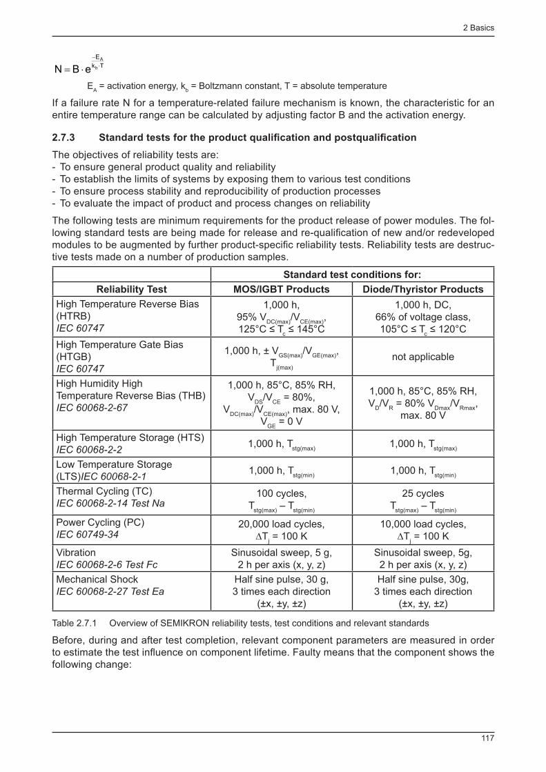
2 Basics
117
Tk
E
b
A
eBN×
-
×=
E A = activation energy, k
b = Boltzmann constant, T = absolute temperature
If a failure rate N for a temperature-related failure mechanism is known, the characteristic for an entire temperature range can be calculated by adjusting factor B and the activation energy.
2.7.3 Standard tests for the product qualifi cation and postqualifi cation
The objectives of reliability tests are: - To ensure general product quality and reliability - To establish the limits of systems by exposing them to various test conditions - To ensure process stability and reproducibility of production processes - To evaluate the impact of product and process changes on reliability
The following tests are minimum requirements for the product release of power modules. The fol-lowing standard tests are being made for release and re-qualifi cation of new and/or redeveloped modules to be augmented by further product-specifi c reliability tests. Reliability tests are destruc-tive tests made on a number of production samples.
Standard test conditions for:
Reliability Test MOS/IGBT Products Diode/Thyristor Products
High Temperature Reverse Bias (HTRB) IEC 60747
1,000 h, 95% V
DC(max) /V
CE(max) ,
125°C ≤ T c ≤ 145°C
1,000 h, DC,66% of voltage class,105°C ≤ T
c ≤ 120°C
High Temperature Gate Bias (HTGB) IEC 60747
1,000 h, ± V GS(max)
/V GE(max)
,T
j(max)
not applicable
High Humidity High Temperature Reverse Bias (THB) IEC 60068-2-67
1,000 h, 85°C, 85% RH,V
DS /V
CE = 80%,
V DC(max)
/V CE(max)
, max. 80 V,V
GE = 0 V
1,000 h, 85°C, 85% RH,V
D /V
R = 80% V
Dmax /V
Rmax ,
max. 80 V
High Temperature Storage (HTS) IEC 60068-2-2
1,000 h, T stg(max)
1,000 h, T stg(max)
Low Temperature Storage (LTS) IEC 60068-2-1
1,000 h, T stg(min)
1,000 h, T stg(min)
Thermal Cycling (TC) IEC 60068-2-14 Test Na
100 cycles,T
stg(max) – T
stg(min)
25 cyclesT
stg(max) – T
stg(min)
Power Cycling (PC) IEC 60749-34
20,000 load cycles, ∆T
j = 100 K
10,000 load cycles,∆T
j = 100 K
Vibration IEC 60068-2-6 Test Fc
Sinusoidal sweep, 5 g,2 h per axis (x, y, z)
Sinusoidal sweep, 5g,2 h per axis (x, y, z)
Mechanical Shock IEC 60068-2-27 Test Ea
Half sine pulse, 30 g, 3 times each direction
(±x, ±y, ±z)
Half sine pulse, 30g, 3 times each direction
(±x, ±y, ±z)
Table 2.7.1 Overview of SEMIKRON reliability tests, test conditions and relevant standards
Before, during and after test completion, relevant component parameters are measured in order to estimate the test infl uence on component lifetime. Faulty means that the component shows the following change:
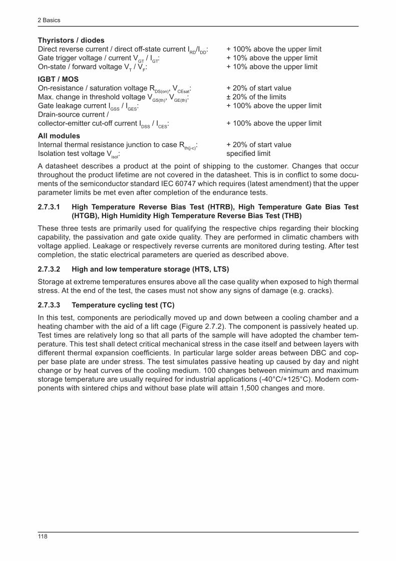
2 Basics
118
Thyristors / diodes
Direct reverse current / direct off-state current I RD
/I DD
: + 100% above the upper limit Gate trigger voltage / current V
GT / I
GT : + 10% above the upper limit
On-state / forward voltage V T / V
F : + 10% above the upper limit
IGBT / MOS
On-resistance / saturation voltage R DS(on)
, V CEsat
: + 20% of start value Max. change in threshold voltage V
GS(th) , V
GE(th) : ± 20% of the limits
Gate leakage current I GSS
/ I GES
: + 100% above the upper limit Drain-source current / collector-emitter cut-off current I
DSS / I
CES : + 100% above the upper limit
All modules
Internal thermal resistance junction to case R th(j-c)
: + 20% of start value Isolation test voltage V
isol : specifi ed limit
A datasheet describes a product at the point of shipping to the customer. Changes that occur throughout the product lifetime are not covered in the datasheet. This is in confl ict to some docu-ments of the semiconductor standard IEC 60747 which requires (latest amendment) that the upper parameter limits be met even after completion of the endurance tests.
2.7.3.1 High Temperature Reverse Bias Test (HTRB), High Temperature Gate Bias Test
(HTGB), High Humidity High Temperature Reverse Bias Test (THB)
These three tests are primarily used for qualifying the respective chips regarding their blocking capability, the passivation and gate oxide quality. They are performed in climatic chambers with voltage applied. Leakage or respectively reverse currents are monitored during testing. After test completion, the static electrical parameters are queried as described above.
2.7.3.2 High and low temperature storage (HTS, LTS)
Storage at extreme temperatures ensures above all the case quality when exposed to high thermal stress. At the end of the test, the cases must not show any signs of damage (e.g. cracks).
2.7.3.3 Temperature cycling test (TC)
In this test, components are periodically moved up and down between a cooling chamber and a heating chamber with the aid of a lift cage (Figure 2.7.2). The component is passively heated up. Test times are relatively long so that all parts of the sample will have adopted the chamber tem-perature. This test shall detect critical mechanical stress in the case itself and between layers with different thermal expansion coeffi cients. In particular large solder areas between DBC and cop-per base plate are under stress. The test simulates passive heating up caused by day and night change or by heat curves of the cooling medium. 100 changes between minimum and maximum storage temperature are usually required for industrial applications (-40°C/+125°C). Modern com-ponents with sintered chips and without base plate will attain 1,500 changes and more.
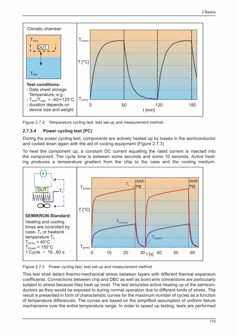
2 Basics
119
Climatic chamber
DUT
Test conditions:- Data sheet storage
Temperature, e.g.:- Tmin/Tmax = -40/+125°C- duration depends on
device size and weight
Tmax
Tmin
T [°C]
T(max)
T(min)
0 60 120 180t [min]
Figure 2.7.2 Temperature cycling test: test set-up and measurement method
2.7.3.4 Power cycling test (PC)
During the power cycling test, components are actively heated up by losses in the semiconductor and cooled down again with the aid of cooling equipment (Figure 2.7.3)
To heat the component up, a constant DC current equalling the rated current is injected into the component. The cycle time is between some seconds and some 10 seconds. Active heat-ing produces a temperature gradient from the chip to the case and the cooling medium.
t [s] 6050403020100
T [°C]
Ts(max)
Ts(min)
Tj
Tj(min)
Tj(max)
cool-ing
cool-ing
SEMIKRON-Standard:
Ts
Heating and coolingtimes are controlled bycase- Tc or heatsinktemperature Ts
Tj(min) = 40°CTj(max) = 150°C1 Cycle ~ 10...60 s
DUT
Figure 2.7.3 Power cycling test: test set-up and measurement method
This test shall detect thermo-mechanical stress between layers with different thermal expansion coeffi cients. Connections between chip and DBC as well as bond wire connections are particularly subject to stress because they heat up most. The test simulates active heating up of the semicon-ductors as they would be exposed to during normal operation due to different kinds of stress. The result is presented in form of characteristic curves for the maximum number of cycles as a function of temperature differences. The curves are based on the simplifi ed assumption of uniform failure mechanisms over the entire temperature range. In order to speed up testing, tests are performed

2 Basics
120
with high ∆T values (e.g. for ∆T = 80 K and ∆T = 110 K) and extrapolated to small temperature dif-ferences to estimate the component lifetime in real applications.
2.7.3.5 Vibration test
Vibration tests are performed in a frequency range between 10 Hz and at least 1000 Hz using an acceleration force of 5 g. Increased acceleration is possible. Depending on the test equipment, there may be limitations regarding the minimum frequency to be used in connection with high ac-celeration. The test purpose is to fi nd weak points in the mechanical construction, for example: - Mechanical aging of spring contacts - Stability of solder contacts in case of vibrating masses - Cracks in cases / structural parts
A low test current monitors safe contact of all auxiliary and main terminals during testing. No ad-ditional vibrating masses (cables, DC-link capacitors) have been fi tted to the samples, as it would often be the case later in real applications. Comparable tests using the set-up of the fi nal applica-tion are recommended and may result in different maximum accelerations.
Figure 2.7.4 SKiiP system on a vibrating plate
2.7.4 Additional tests for spring contacts
Additional tests for contact reliability even under extreme conditions are performed to qualify spring contacts [44].
2.7.4.1 Micro-vibration (fretting corrosion)
Contact surfaces may corrode under electrical load and the infl uence of micro-vibrations. Material abrasion is caused which may result in contact failure. The test objective is to check whether good electrical contact is ensured for the specifi c combination of spring material and recommended con-tact surface of the PCB until the end of service life. The test simulates vibrations through a piezo actuator (Figure 2.7.5) (frequency: 1 Hz, amplitude: 50 µm). The contacts are monitored during testing. In order to suppress "clean-burning" of the contacts (i.e. re-establishing good contact), currents are limited to 20 mA and voltages to 20 mV.
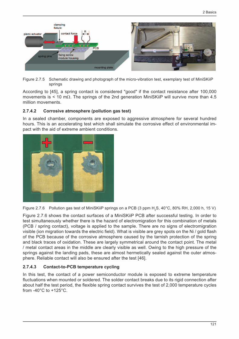
2 Basics
121
Figure 2.7.5 Schematic drawing and photograph of the micro-vibration test, exemplary test of MiniSKiiP springs
According to [45], a spring contact is considered "good" if the contact resistance after 100,000 movements is < 10 mΩ. The springs of the 2nd generation MiniSKiiP will survive more than 4.5 million movements.
2.7.4.2 Corrosive atmosphere (pollution gas test)
In a sealed chamber, components are exposed to aggressive atmosphere for several hundred hours. This is an accelerating test which shall simulate the corrosive effect of environmental im-pact with the aid of extreme ambient conditions.
Figure 2.7.6 Pollution gas test of MiniSKiiP springs on a PCB (3 ppm H 2 S, 40°C, 80% RH, 2,000 h, 15 V)
Figure 2.7.6 shows the contact surfaces of a MiniSKiiP PCB after successful testing. In order to test simultaneously whether there is the hazard of electromigration for this combination of metals (PCB / spring contact), voltage is applied to the sample. There are no signs of electromigration visible (ion migration towards the electric fi eld). What is visible are grey spots on the Ni / gold fl ash of the PCB because of the corrosive atmosphere caused by the tarnish protection of the spring and black traces of oxidation. These are largely symmetrical around the contact point. The metal / metal contact areas in the middle are clearly visible as well. Owing to the high pressure of the springs against the landing pads, these are almost hermetically sealed against the outer atmos-phere. Reliable contact will also be ensured after the test [46].
2.7.4.3 Contact-to-PCB temperature cycling
In this test, the contact of a power semiconductor module is exposed to extreme temperature fl uctuations when mounted or soldered. The solder contact breaks due to its rigid connection after about half the test period, the fl exible spring contact survives the test of 2,000 temperature cycles from -40°C to +125°C.
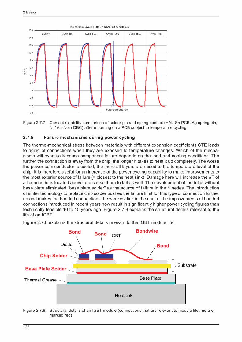
2 Basics
122
Temperature cycling -40°C / 125°C, 30 min/30 min
-60
-40
-20
0
20
40
60
80
100
120
140
160
T[°
C]
Cycle 1 Cycle 100 Cycle 500 Cycle 1000 Cycle 1500 Cycle 2000
Failure of solder pin
Figure 2.7.7 Contact reliability comparison of solder pin and spring contact (HAL-Sn PCB, Ag spring pin, Ni / Au-fl ash DBC) after mounting on a PCB subject to temperature cycling.
2.7.5 Failure mechanisms during power cycling
The thermo-mechanical stress between materials with different expansion coeffi cients CTE leads to aging of connections when they are exposed to temperature changes. Which of the mecha-nisms will eventually cause component failure depends on the load and cooling conditions. The further the connection is away from the chip, the longer it takes to heat it up completely. The worse the power semiconductor is cooled, the more all layers are raised to the temperature level of the chip. It is therefore useful for an increase of the power cycling capability to make improvements to the most exterior source of failure (= closest to the heat sink). Damage here will increase the ∆T of all connections located above and cause them to fail as well. The development of modules without base plate eliminated "base plate solder" as the source of failure in the Nineties. The introduction of sinter technology to replace chip solder pushes the failure limit for this type of connection further up and makes the bonded connections the weakest link in the chain. The improvements of bonded connections introduced in recent years now result in signifi cantly higher power cycling fi gures than technically feasible 10 to 15 years ago. Figure 2.7.8 explains the structural details relevant to the life of an IGBT.
Figure 2.7.8 explains the structural details relevant to the IGBT module life.
Substrate
Base Plate
IGBT
Diode
Chip Solder
Base Plate Solder
Thermal Grease
Heatsink
BondwireBond Bond
Bond
Figure 2.7.8 Structural details of an IGBT module (connections that are relevant to module lifetime are marked red)
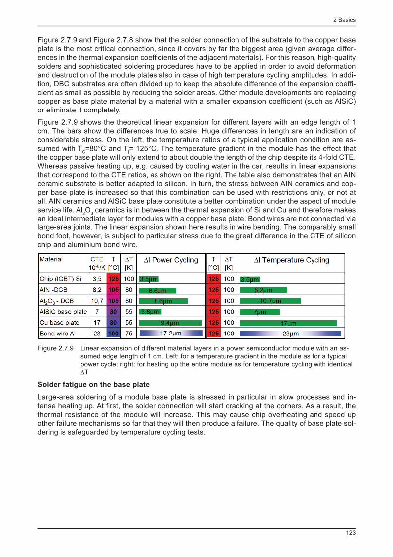
2 Basics
123
Figure 2.7.9 and Figure 2.7.8 show that the solder connection of the substrate to the copper base plate is the most critical connection, since it covers by far the biggest area (given average differ-ences in the thermal expansion coeffi cients of the adjacent materials). For this reason, high-quality solders and sophisticated soldering procedures have to be applied in order to avoid deformation and destruction of the module plates also in case of high temperature cycling amplitudes. In addi-tion, DBC substrates are often divided up to keep the absolute difference of the expansion coeffi -cient as small as possible by reducing the solder areas. Other module developments are replacing copper as base plate material by a material with a smaller expansion coeffi cient (such as AlSiC) or eliminate it completely.
Figure 2.7.9 shows the theoretical linear expansion for different layers with an edge length of 1 cm. The bars show the differences true to scale. Huge differences in length are an indication of considerable stress. On the left, the temperature ratios of a typical application condition are as-sumed with T
C =80°C and T
j = 125°C. The temperature gradient in the module has the effect that
the copper base plate will only extend to about double the length of the chip despite its 4-fold CTE. Whereas passive heating up, e.g. caused by cooling water in the car, results in linear expansions that correspond to the CTE ratios, as shown on the right. The table also demonstrates that an AIN ceramic substrate is better adapted to silicon. In turn, the stress between AIN ceramics and cop-per base plate is increased so that this combination can be used with restrictions only, or not at all. AIN ceramics and AlSiC base plate constitute a better combination under the aspect of module service life. Al
2 O
3 ceramics is in between the thermal expansion of Si and Cu and therefore makes
an ideal intermediate layer for modules with a copper base plate. Bond wires are not connected via large-area joints. The linear expansion shown here results in wire bending. The comparably small bond foot, however, is subject to particular stress due to the great difference in the CTE of silicon chip and aluminium bond wire.
Figure 2.7.9 Linear expansion of different material layers in a power semiconductor module with an as-sumed edge length of 1 cm. Left: for a temperature gradient in the module as for a typical power cycle; right: for heating up the entire module as for temperature cycling with identical ∆T
Solder fatigue on the base plate
Large-area soldering of a module base plate is stressed in particular in slow processes and in-tense heating up. At fi rst, the solder connection will start cracking at the corners. As a result, the thermal resistance of the module will increase. This may cause chip overheating and speed up other failure mechanisms so far that they will then produce a failure. The quality of base plate sol-dering is safeguarded by temperature cycling tests.
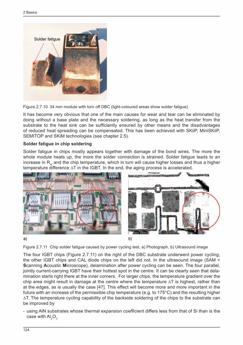
2 Basics
124
Solder fatigue
Figure 2.7.10 34 mm module with torn off DBC (light-coloured areas show solder fatigue)
It has become very obvious that one of the main causes for wear and tear can be eliminated by doing without a base plate and the necessary soldering, as long as the heat transfer from the substrate to the heat sink can be suffi ciently ensured by other means and the disadvantages of reduced heat spreading can be compensated. This has been achieved with SKiiP, MiniSKiiP, SEMITOP and SKiM technologies (see chapter 2.5).
Solder fatigue in chip soldering
Solder fatigue in chips mostly appears together with damage of the bond wires. The more the whole module heats up, the more the solder connection is strained. Solder fatigue leads to an increase in R
th and the chip temperature, which in turn will cause higher losses and thus a higher
temperature difference ∆T in the IGBT. In the end, the aging process is accelerated.
Figure 2.7.11 Chip solder fatigue caused by power cycling test, a) Photograph, b) Ultrasound image
The four IGBT chips (Figure 2.7.11) on the right of the DBC substrate underwent power cycling, the other IGBT chips and CAL diode chips on the left did not. In the ultrasound image (SAM = S canning A coustic M icroscope), delamination after power cycling can be seen. The four parallel, jointly current-carrying IGBT have their hottest spot in the centre. It can be clearly seen that dela-mination starts right there at the inner corners. For larger chips, the temperature gradient over the chip area might result in damage at the centre where the temperature ∆T is highest, rather than at the edges, as is usually the case [47]. This effect will become more and more important in the future with an increase of the permissible chip temperature (e.g. to 175°C) and the resulting higher ∆T. The temperature cycling capability of the backside soldering of the chips to the substrate can be improved by
- using AlN substrates whose thermal expansion coeffi cient differs less from that of Si than is the case with Al
2 O
3
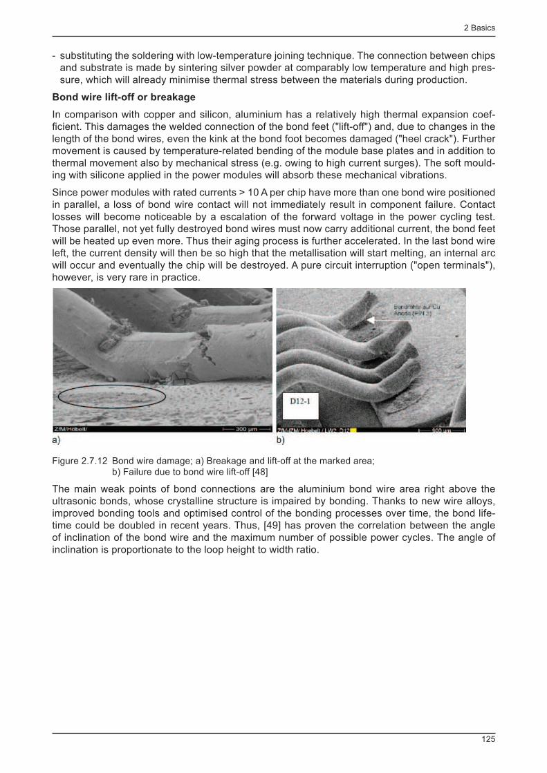
2 Basics
125
- substituting the soldering with low-temperature joining technique. The connection between chips and substrate is made by sintering silver powder at comparably low temperature and high pres-sure, which will already minimise thermal stress between the materials during production.
Bond wire lift-off or breakage
In comparison with copper and silicon, aluminium has a relatively high thermal expansion coef-fi cient. This damages the welded connection of the bond feet ("lift-off") and, due to changes in the length of the bond wires, even the kink at the bond foot becomes damaged ("heel crack"). Further movement is caused by temperature-related bending of the module base plates and in addition to thermal movement also by mechanical stress (e.g. owing to high current surges). The soft mould-ing with silicone applied in the power modules will absorb these mechanical vibrations.
Since power modules with rated currents > 10 A per chip have more than one bond wire positioned in parallel, a loss of bond wire contact will not immediately result in component failure. Contact losses will become noticeable by a escalation of the forward voltage in the power cycling test. Those parallel, not yet fully destroyed bond wires must now carry additional current, the bond feet will be heated up even more. Thus their aging process is further accelerated. In the last bond wire left, the current density will then be so high that the metallisation will start melting, an internal arc will occur and eventually the chip will be destroyed. A pure circuit interruption ("open terminals"), however, is very rare in practice.
Figure 2.7.12 Bond wire damage; a) Breakage and lift-off at the marked area; b) Failure due to bond wire lift-off [48]
The main weak points of bond connections are the aluminium bond wire area right above the ultrasonic bonds, whose crystalline structure is impaired by bonding. Thanks to new wire alloys, improved bonding tools and optimised control of the bonding processes over time, the bond life-time could be doubled in recent years. Thus, [49] has proven the correlation between the angle of inclination of the bond wire and the maximum number of possible power cycles. The angle of inclination is proportionate to the loop height to width ratio.
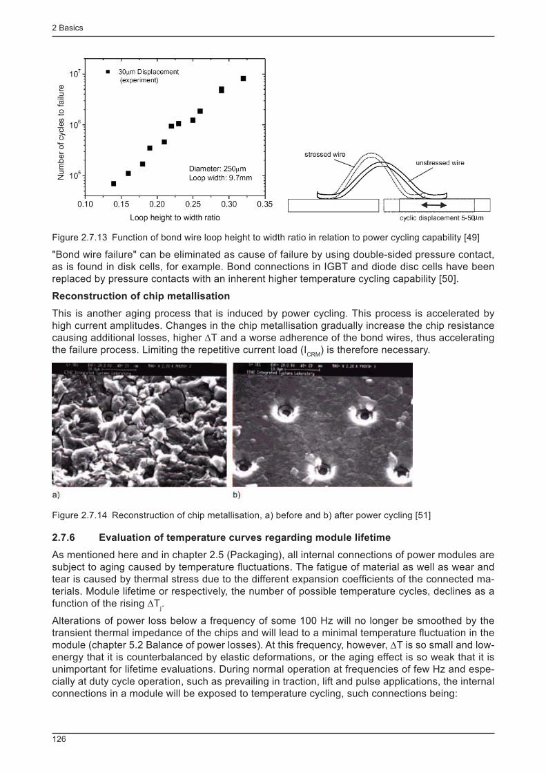
2 Basics
126
Figure 2.7.13 Function of bond wire loop height to width ratio in relation to power cycling capability [49]
"Bond wire failure" can be eliminated as cause of failure by using double-sided pressure contact, as is found in disk cells, for example. Bond connections in IGBT and diode disc cells have been replaced by pressure contacts with an inherent higher temperature cycling capability [50].
Reconstruction of chip metallisation
This is another aging process that is induced by power cycling. This process is accelerated by high current amplitudes. Changes in the chip metallisation gradually increase the chip resistance causing additional losses, higher ∆T and a worse adherence of the bond wires, thus accelerating the failure process. Limiting the repetitive current load (I
CRM ) is therefore necessary.
Figure 2.7.14 Reconstruction of chip metallisation, a) before and b) after power cycling [51]
2.7.6 Evaluation of temperature curves regarding module lifetime
As mentioned here and in chapter 2.5 (Packaging), all internal connections of power modules are subject to aging caused by temperature fl uctuations. The fatigue of material as well as wear and tear is caused by thermal stress due to the different expansion coeffi cients of the connected ma-terials. Module lifetime or respectively, the number of possible temperature cycles, declines as a function of the rising ∆T
j .
Alterations of power loss below a frequency of some 100 Hz will no longer be smoothed by the transient thermal impedance of the chips and will lead to a minimal temperature fl uctuation in the module (chapter 5.2 Balance of power losses). At this frequency, however, ∆T is so small and low-energy that it is counterbalanced by elastic deformations, or the aging effect is so weak that it is unimportant for lifetime evaluations. During normal operation at frequencies of few Hz and espe-cially at duty cycle operation, such as prevailing in traction, lift and pulse applications, the internal connections in a module will be exposed to temperature cycling, such connections being:
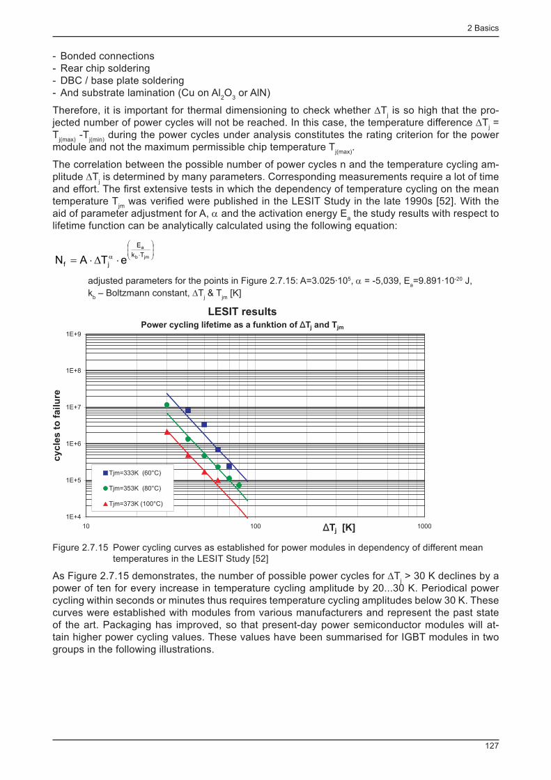
2 Basics
127
- Bonded connections - Rear chip soldering - DBC / base plate soldering - And substrate lamination (Cu on Al
2 O
3 or AlN)
Therefore, it is important for thermal dimensioning to check whether ∆T j is so high that the pro-
jected number of power cycles will not be reached. In this case, the temperature difference ∆T j =
T j(max)
-T j(min)
during the power cycles under analysis constitutes the rating criterion for the power module and not the maximum permissible chip temperature T
j(max) .
The correlation between the possible number of power cycles n and the temperature cycling am-plitude ∆T
j is determined by many parameters. Corresponding measurements require a lot of time
and effort. The fi rst extensive tests in which the dependency of temperature cycling on the mean temperature T
jm was verifi ed were published in the LESIT Study in the late 1990s [52]. With the
aid of parameter adjustment for A, α and the activation energy E a the study results with respect to
lifetime function can be analytically calculated using the following equation:
÷÷ø
öççè
æ
×a ×D×= jmb
a
Tk
E
jf eTAN
adjusted parameters for the points in Figure 2.7.15: A=3.025·10 5 , α = -5,039, E a =9.891·10 -20 J,
k b – Boltzmann constant, ∆T
j & T
jm [K]
LESIT resultsPower cycling lifetime as a funktion of TΔ j and Tjm
1E+4
1E+5
1E+6
1E+7
1E+8
1E+9
10 100 1000TΔ j [K]
cy
cle
sto
fail
ure
Tjm=333K (60°C)
Tjm=353K (80°C)
Tjm=373K (100°C)
Figure 2.7.15 Power cycling curves as established for power modules in dependency of different mean temperatures in the LESIT Study [52]
As Figure 2.7.15 demonstrates, the number of possible power cycles for ∆T j > 30 K declines by a
power of ten for every increase in temperature cycling amplitude by 20...30 K. Periodical power cycling within seconds or minutes thus requires temperature cycling amplitudes below 30 K. These curves were established with modules from various manufacturers and represent the past state of the art. Packaging has improved, so that present-day power semiconductor modules will at-tain higher power cycling values. These values have been summarised for IGBT modules in two groups in the following illustrations.
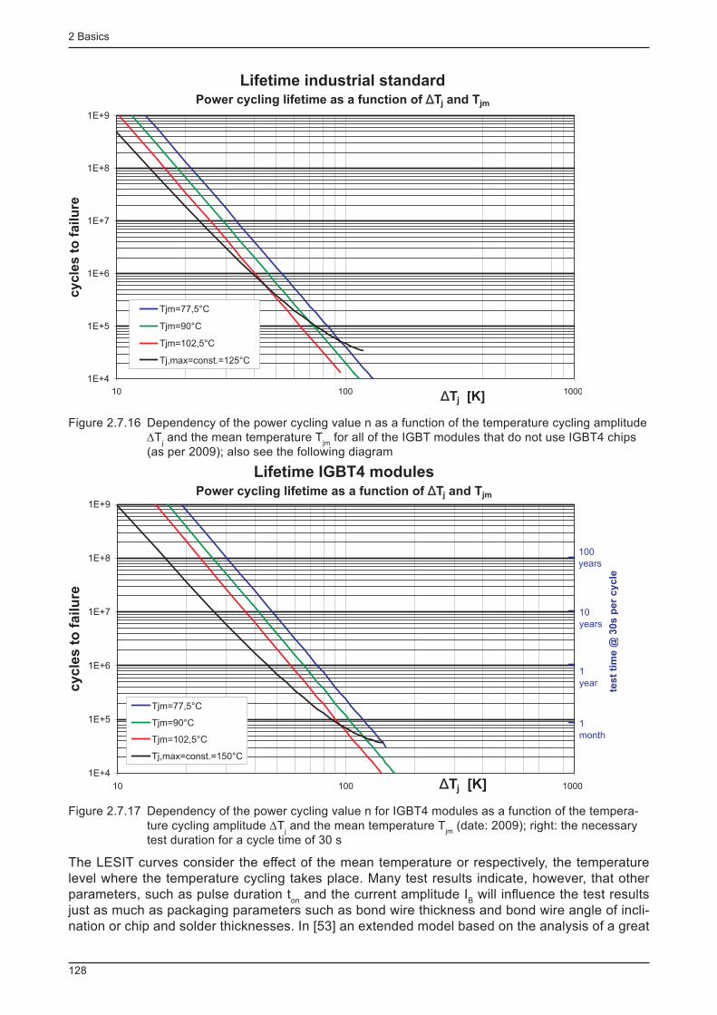
2 Basics
128
Lifetime industrial standardPower cycling lifetime as a function of TΔ j and Tjm
1E+4
1E+5
1E+6
1E+7
1E+8
1E+9
10 100 1000TΔ j [K]
cycle
sto
failu
re
Tjm=77,5°C
Tjm=90°C
Tjm=102,5°C
Tj,max=const.=125°C
Figure 2.7.16 Dependency of the power cycling value n as a function of the temperature cycling amplitude ∆T
j and the mean temperature T
jm for all of the IGBT modules that do not use IGBT4 chips
(as per 2009); also see the following diagram
Lifetime IGBT4 modulesPower cycling lifetime as a function of TΔ j and Tjm
1E+4
1E+5
1E+6
1E+7
1E+8
1E+9
10 100 1000TΔ j [K]
cycle
sto
failu
re
test
tim
e@
30s
per
cycle
Tjm=77,5°C
Tjm=90°C
Tjm=102,5°C
Tj,max=const.=150°C
1
month
1
year
10
years
100
years
Figure 2.7.17 Dependency of the power cycling value n for IGBT4 modules as a function of the tempera-ture cycling amplitude ∆T
j and the mean temperature T
jm (date: 2009); right: the necessary
test duration for a cycle time of 30 s
The LESIT curves consider the effect of the mean temperature or respectively, the temperature level where the temperature cycling takes place. Many test results indicate, however, that other parameters, such as pulse duration t
on and the current amplitude I
B will infl uence the test results
just as much as packaging parameters such as bond wire thickness and bond wire angle of incli-nation or chip and solder thicknesses. In [53] an extended model based on the analysis of a great

2 Basics
129
number of tests is shown. Parameters, validity limits and coeffi cients are listed in the following table:
65431 DVIt)273T(
expTAN CBon
min,j
2jf
bbbbb ××××÷÷ø
öççè
æ
+b
×D×=
Parameters Symbol Unit Limits Coeffi cient Value Comment
Technology Factor A 2.03E+14 Standard
Technology Factor A 9.34E+14 IGBT4
Temperature difference ∆T K 45…150 β1 -4.416
Min. chip temperature T j(min)
°C 20…120 β2 1285
Pulse duration t on
s 1…15 β3 -0.463
Current per bond foot I B
A 3…23 β4 -0.716
Voltage class/100 V C
V 6…33 β5 -0.761
Bond wire diameter D µm 75…500 β6 -0.5
Table 2.7.2 Parameters and limits for the calculation of power cycles using the equation above
Example: Let us assume a given number of power cycles N f and a test duration t
on(test) . If a compo-
nent would be used for a different pulse duration t on(application)
in the application, this would equal to
3
)test(on
)napplicatio(on
testnapplicatiot
tNN
b
÷÷ø
öççè
æ×=
This means, if the application pulse duration is 1/10 of the test pulse duration, the lifetime would roughly triple. This model gives a good impression of the impact of various parameters on power cycling fi gures, but it is only suitable to a limited extent in order to calculate concrete lifetime val-ues isolated from any other parameter. The reason are physical constraints, since not all of the parameters are independent of each other. For example, a small ∆T
j is not possible in the event of
high currents and long pulse durations. Or, as assumed for the pulse duration in our example, an identical ∆T would require different current values for different pulse durations t
on .

2 Basics
130

3 Datasheet Ratings for MOSFET, IGBT, Diodes and Thyristors
131
3 Datasheet Ratings for MOSFET, IGBT, Diodes and
Thyristors
3.1 Standards, symbols and terms
3.1.1 Standards
The practical usage of symbols and terms and their meaning is described in the international standard IEC 60747 "Discrete Semiconductor Devices". Detailed information on the parameters, minimum requirements for datasheet ratings and test methods is provided in the standard's pro-duct-specifi c sections. - IEC 60747-1 General (letter symbols and terms) - IEC 60747-2 Diodes - IEC 60747-3 Thyristors - IEC 60747-8 Field effect transistors - IEC 60747-9 IGBT - IEC 60747-15 Isolated power semiconductor devices
Other important standards applicable to semiconductor devices: - IEC 60191-2 Mechanical standardisation of semiconductor devices, Part 2: Dimensions (standardised case drawings)
- DIN EN 50178 Electronic equipment for use in power installations (insulation tests, partial discharge)
- IEC 60664 Insulation coordination for equipment within low-voltage systems (clearance and creepage distances)
- IEC 60721 Classifi cation of environmental conditions - IEC 60068 Environmental testing (specifi cation of test conditions) - IEC 60749 Mechanical and climatic test methods
The following specifi cations and standards do not correspond with international standards in use, but are applicable to particular markets: - UL94 Flammability tests for plastic parts used in devices and appliances - UL508C Power conversion equipment - MIL-STD-750E Test methods for semiconductor devices
3.1.2 Letter symbols and terms
Voltages: Two index letters are used to designate the terminals between which the applied voltage is measured. If the potential of the terminal designated with the fi rst index letter is positive versus the terminal designated with the second index letter (reference potential), the applied voltage is positive, e.g. V
CE .
- C collector - E emitter - G gate - D drain - S source - K cathode - A anode
For diodes, the forward on-state voltage is indexed with "F" rather than "AK" ("forward" positive anode potential versus cathode potential); "R" is used to designate the reverse blocking voltage ("reverse" positive cathode potential versus anode potential). In the case of transistors, an addi-tional third index letter may be used to determine the wiring status between the terminal with index 2 and a non-designated third terminal, e.g. V
CES indicates that the IGBT is "short-circuited between
gate and emitter". The following abbreviations are permissible:
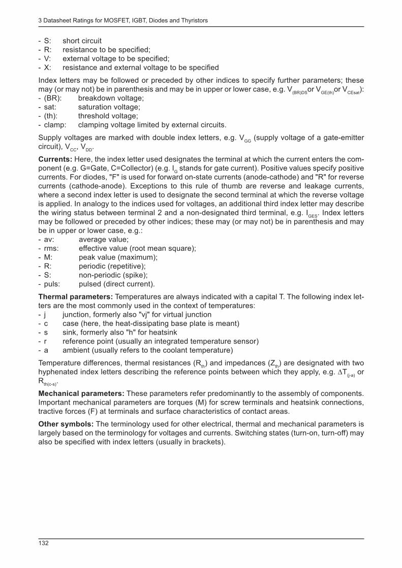
3 Datasheet Ratings for MOSFET, IGBT, Diodes and Thyristors
132
- S: short circuit - R: resistance to be specifi ed; - V: external voltage to be specifi ed; - X: resistance and external voltage to be specifi ed
Index letters may be followed or preceded by other indices to specify further parameters; these may (or may not) be in parenthesis and may be in upper or lower case, e.g. V
(BR)DS or V
GE(th) or V
CEsat ):
- (BR): breakdown voltage; - sat: saturation voltage; - (th): threshold voltage; - clamp: clamping voltage limited by external circuits.
Supply voltages are marked with double index letters, e.g. V GG
(supply voltage of a gate-emitter circuit), V
CC , V
DD .
Currents: Here, the index letter used designates the terminal at which the current enters the com-ponent (e.g. G=Gate, C=Collector) (e.g. I
G stands for gate current). Positive values specify positive
currents. For diodes, "F" is used for forward on-state currents (anode-cathode) and "R" for reverse currents (cathode-anode). Exceptions to this rule of thumb are reverse and leakage currents, where a second index letter is used to designate the second terminal at which the reverse voltage is applied. In analogy to the indices used for voltages, an additional third index letter may describe the wiring status between terminal 2 and a non-designated third terminal, e.g. I
GES . Index letters
may be followed or preceded by other indices; these may (or may not) be in parenthesis and may be in upper or lower case, e.g.: - av: average value; - rms: effective value (root mean square); - M: peak value (maximum); - R: periodic (repetitive); - S: non-periodic (spike); - puls: pulsed (direct current).
Thermal parameters: Temperatures are always indicated with a capital T. The following index let-ters are the most commonly used in the context of temperatures: - j junction, formerly also "vj" for virtual junction - c case (here, the heat-dissipating base plate is meant) - s sink, formerly also "h" for heatsink - r reference point (usually an integrated temperature sensor) - a ambient (usually refers to the coolant temperature)
Temperature differences, thermal resistances (R th ) and impedances (Z
th ) are designated with two
hyphenated index letters describing the reference points between which they apply, e.g. ∆T (j-a)
or R
th(c-s) .
Mechanical parameters: These parameters refer predominantly to the assembly of components. Important mechanical parameters are torques (M) for screw terminals and heatsink connections, tractive forces (F) at terminals and surface characteristics of contact areas.
Other symbols: The terminology used for other electrical, thermal and mechanical parameters is largely based on the terminology for voltages and currents. Switching states (turn-on, turn-off) may also be specifi ed with index letters (usually in brackets).
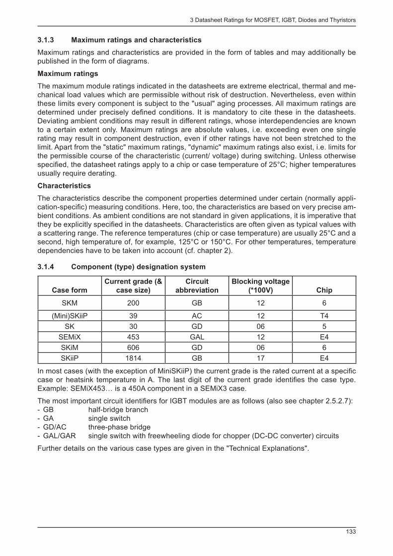
3 Datasheet Ratings for MOSFET, IGBT, Diodes and Thyristors
133
3.1.3 Maximum ratings and characteristics
Maximum ratings and characteristics are provided in the form of tables and may additionally be published in the form of diagrams.
Maximum ratings
The maximum module ratings indicated in the datasheets are extreme electrical, thermal and me-chanical load values which are permissible without risk of destruction. Nevertheless, even within these limits every component is subject to the "usual" aging processes. All maximum ratings are determined under precisely defi ned conditions. It is mandatory to cite these in the datasheets. Deviating ambient conditions may result in different ratings, whose interdependencies are known to a certain extent only. Maximum ratings are absolute values, i.e. exceeding even one single rating may result in component destruction, even if other ratings have not been stretched to the limit. Apart from the "static" maximum ratings, "dynamic" maximum ratings also exist, i.e. limits for the permissible course of the characteristic (current/ voltage) during switching. Unless otherwise specifi ed, the datasheet ratings apply to a chip or case temperature of 25°C; higher temperatures usually require derating.
Characteristics
The characteristics describe the component properties determined under certain (normally appli-cation-specifi c) measuring conditions. Here, too, the characteristics are based on very precise am-bient conditions. As ambient conditions are not standard in given applications, it is imperative that they be explicitly specifi ed in the datasheets. Characteristics are often given as typical values with a scattering range. The reference temperatures (chip or case temperature) are usually 25°C and a second, high temperature of, for example, 125°C or 150°C. For other temperatures, temperature dependencies have to be taken into account (cf. chapter 2).
3.1.4 Component (type) designation system
Case form
Current grade (&
case size)
Circuit
abbreviation
Blocking voltage
(*100V) Chip
SKM 200 GB 12 6
(Mini)SKiiP 39 AC 12 T4
SK 30 GD 06 5
SEMiX 453 GAL 12 E4
SKiM 606 GD 06 6
SKiiP 1814 GB 17 E4
In most cases (with the exception of MiniSKiiP) the current grade is the rated current at a specifi c case or heatsink temperature in A. The last digit of the current grade identifi es the case type. Example: SEMiX453… is a 450A component in a SEMiX3 case.
The most important circuit identifi ers for IGBT modules are as follows (also see chapter 2.5.2.7): - GB half-bridge branch - GA single switch - GD/AC three-phase bridge - GAL/GAR single switch with freewheeling diode for chopper (DC-DC converter) circuits
Further details on the various case types are given in the "Technical Explanations".
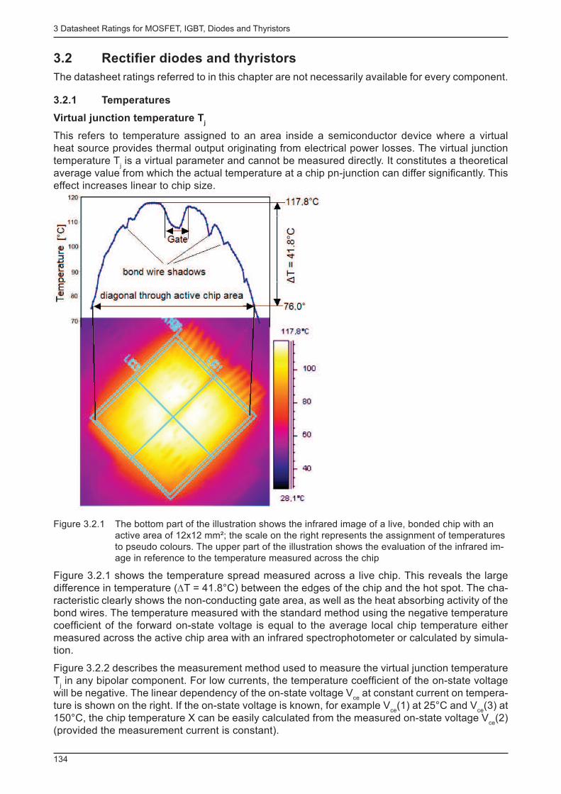
3 Datasheet Ratings for MOSFET, IGBT, Diodes and Thyristors
134
3.2 Rectifi er diodes and thyristors
The datasheet ratings referred to in this chapter are not necessarily available for every component.
3.2.1 Temperatures
Virtual junction temperature T j
This refers to temperature assigned to an area inside a semiconductor device where a virtual heat source provides thermal output originating from electrical power losses. The virtual junction temperature T
j is a virtual parameter and cannot be measured directly. It constitutes a theoretical
average value from which the actual temperature at a chip pn-junction can differ signifi cantly. This effect increases linear to chip size.
Figure 3.2.1 The bottom part of the illustration shows the infrared image of a live, bonded chip with an active area of 12x12 mm²; the scale on the right represents the assignment of temperatures to pseudo colours. The upper part of the illustration shows the evaluation of the infrared im-age in reference to the temperature measured across the chip
Figure 3.2.1 shows the temperature spread measured across a live chip. This reveals the large difference in temperature (∆T = 41.8°C) between the edges of the chip and the hot spot. The cha-racteristic clearly shows the non-conducting gate area, as well as the heat absorbing activity of the bond wires. The temperature measured with the standard method using the negative temperature coeffi cient of the forward on-state voltage is equal to the average local chip temperature either measured across the active chip area with an infrared spectrophotometer or calculated by simula-tion.
Figure 3.2.2 describes the measurement method used to measure the virtual junction temperature T
j in any bipolar component. For low currents, the temperature coeffi cient of the on-state voltage
will be negative. The linear dependency of the on-state voltage V ce
at constant current on tempera-ture is shown on the right. If the on-state voltage is known, for example V
ce (1) at 25°C and V
ce(3) at
150°C, the chip temperature X can be easily calculated from the measured on-state voltage V ce
(2) (provided the measurement current is constant).
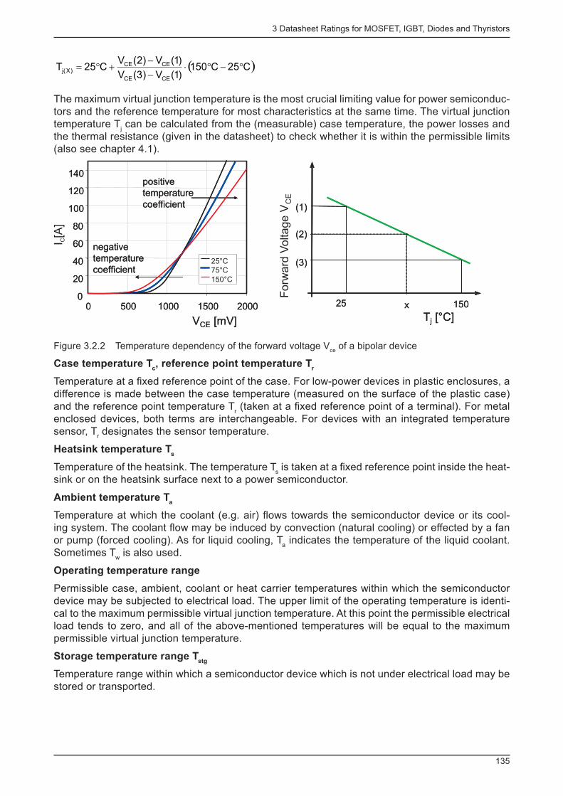
3 Datasheet Ratings for MOSFET, IGBT, Diodes and Thyristors
135
( )C25C150
)1(V)3(V
)1(V)2(VC25T
CECE
CECE)X(j °-°×
--
+°=
The maximum virtual junction temperature is the most crucial limiting value for power semiconduc-tors and the reference temperature for most characteristics at the same time. The virtual junction temperature T
j can be calculated from the (measurable) case temperature, the power losses and
the thermal resistance (given in the datasheet) to check whether it is within the permissible limits (also see chapter 4.1).
Tj [°C]
25 150x
(1)
(2)
(3)
Tj [°C]
Forw
ard
Voltage
VC
E
25 150x
(1)
(2)
(3)
0
20
40
60
80
100
120
140
0 500 1000 1500 2000
VCE [mV]
25°C
75°C
150°C
positive
temperature
coefficient
negative
temperature
coefficient
0
20
40
60
80
100
120
140
0 500 1000 1500 2000
VCE [mV]
I[A
]C
25°C
75°C
150°C
positive
temperature
coefficient
negative
temperature
coefficient
Figure 3.2.2 Temperature dependency of the forward voltage V ce
of a bipolar device
Case temperature T c , reference point temperature T
r
Temperature at a fi xed reference point of the case. For low-power devices in plastic enclosures, a difference is made between the case temperature (measured on the surface of the plastic case) and the reference point temperature T
r (taken at a fi xed reference point of a terminal). For metal
enclosed devices, both terms are interchangeable. For devices with an integrated temperature sensor, T
r designates the sensor temperature.
Heatsink temperature T s
Temperature of the heatsink. The temperature T s is taken at a fi xed reference point inside the heat-
sink or on the heatsink surface next to a power semiconductor.
Ambient temperature T a
Temperature at which the coolant (e.g. air) fl ows towards the semiconductor device or its cool-ing system. The coolant fl ow may be induced by convection (natural cooling) or effected by a fan or pump (forced cooling). As for liquid cooling, T
a indicates the temperature of the liquid coolant.
Sometimes T w is also used.
Operating temperature range
Permissible case, ambient, coolant or heat carrier temperatures within which the semiconductor device may be subjected to electrical load. The upper limit of the operating temperature is identi-cal to the maximum permissible virtual junction temperature. At this point the permissible electrical load tends to zero, and all of the above-mentioned temperatures will be equal to the maximum permissible virtual junction temperature.
Storage temperature range T stg
Temperature range within which a semiconductor device which is not under electrical load may be stored or transported.
3 Datasheet Ratings for MOSFET, IGBT, Diodes and Thyristors
136
3.2.2 Thermal impedance and thermal resistance
The thermal impedance is defi ned as a quotient of the time function of a temperature difference divided by the impressed power dissipation. In the datasheets this value is given as a function of time in the form of a diagram.
P
)t(T)t(T)t(Z 21
th
-=
The static upper range value is the actual thermal resistance. This is indicated in the datasheets in the form of a characteristic. Depending on the choice of temperature detection points, distinctions are made. For example: - Z
th(j-c) / R
th(j-c) junction-case
- Z th(c-s)
/ R th(c-s)
case-heatsink - Z
th(s-a) / R
th(s-a) heatsink-ambient
- Z th(j-a)
/ R th(j-a)
junction-ambient
Since T c and T
s depend on the position of the detection point, their shares of the total thermal resist-
ance may vary. The total thermal resistance, however, is always calculated as follows (this also applies to Z
th ):
R th(j-c)
+ R th(c-s)
+ R th(s-a)
= R th(j-a)
The thermal resistance may be used to calculate true constant quantities, as well as average tem-peratures of periodic functions. Normally, however, the current conducted through a semiconductor device and, consequently, the power losses, are time-dependent parameters. In line rectifi ers, the losses and temperatures vary within the bounds of the line frequency around a mean value. The virtual junction temperature T
j is higher under peak load than under direct current load or if calcu-
lated with a mean power loss P FAV
/P TAV
and R th . The temperature fl uctuation range depends on the
current waveform and the current fl ow time within a cycle. With help of the thermal impedance, the effective junction temperature T
j (t) can be calculated for any given duration of power dissipation.
The datasheets of older components still contain auxiliary values. This is owing to the restricted methods of calculation at that time. These values should enable the user to factor in the load-dependent power loss and temperature fl uctuation based on the operating frequency. Although not correct from a physics point of view, the static resistance R
th is used as a mathematical aid and
is multiplied by a corrective factor in order to project the mean temperature to the maximum tem-perature value (Figure 3.2.3). The resulting value R
th , which is given either as a pure operand or
in the form of a diagram, applies to the given current waveform and the lead angle for a frequency range of 40…60 Hz. In other words, Rec120 stands for "rectangular current with a current fl ow time of 120°".
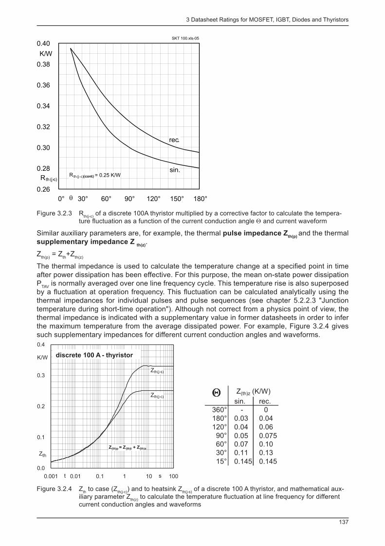
3 Datasheet Ratings for MOSFET, IGBT, Diodes and Thyristors
137
0.26
0.28
0.30
0.32
0.34
0.36
0.38
0.40
0° 30° 60° 90° 120° 150° 180°q
R th (j -c)
K/W
rec.
sin.R th (j -c)(cont.) = 0.25 K/W
SKT 100.xls-05
Figure 3.2.3 R th(j-c)
of a discrete 100A thyristor multiplied by a corrective factor to calculate the tempera-ture fl uctuation as a function of the current conduction angle Θ and current waveform
Similar auxiliary parameters are, for example, the thermal pulse impedance Z th(p)
and the thermal supplementary impedance Z
th(z) .
Z th(p)
= Z th +Z
th(z)
The thermal impedance is used to calculate the temperature change at a specifi ed point in time after power dissipation has been effective. For this purpose, the mean on-state power dissipation P
TAV is normally averaged over one line frequency cycle. This temperature rise is also superposed
by a fl uctuation at operation frequency. This fl uctuation can be calculated analytically using the thermal impedances for individual pulses and pulse sequences (see chapter 5.2.2.3 "Junction temperature during short-time operation"). Although not correct from a physics point of view, the thermal impedance is indicated with a supplementary value in former datasheets in order to infer the maximum temperature from the average dissipated power. For example, Figure 3.2.4 gives such supplementary impedances for different current conduction angles and waveforms.
sin. rec.
360° - 0
180° 0.04
120° 0.06
90°
60° 0.10
30° 0.13
15°
Z(th)z (K/W)Q
0.0
0.1
0.2
0.3
0.4
0.001 0.01 0.1 1 10 100s
Zth
K/W
t
Zth(j-s)
Zth(j-c)
Z(th)p = Z(th)t + Z(th)z
diskreter Thyristordiscrete 100 A - thyristor
0.075
0.145
0.03
0.04
0.07
0.11
0.05
0.145
Figure 3.2.4 Z th to case (Z
th(j-c) ) and to heatsink Z
th(j-s) of a discrete 100 A thyristor, and mathematical aux-
iliary parameter Z th(z)
to calculate the temperature fl uctuation at line frequency for different current conduction angles and waveforms
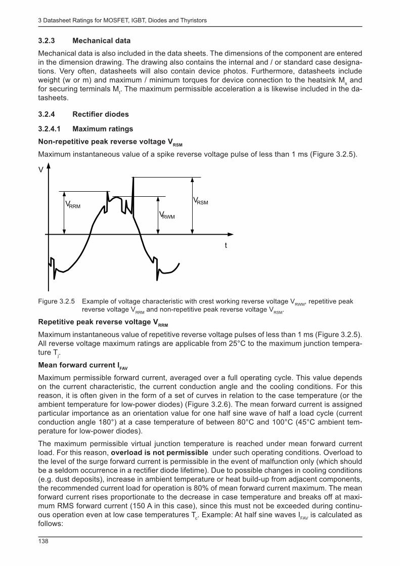
3 Datasheet Ratings for MOSFET, IGBT, Diodes and Thyristors
138
3.2.3 Mechanical data
Mechanical data is also included in the data sheets. The dimensions of the component are entered in the dimension drawing. The drawing also contains the internal and / or standard case designa-tions. Very often, datasheets will also contain device photos. Furthermore, datasheets include weight (w or m) and maximum / minimum torques for device connection to the heatsink M
s and
for securing terminals M t . The maximum permissible acceleration a is likewise included in the da-
tasheets.
3.2.4 Rectifi er diodes
3.2.4.1 Maximum ratings
Non-repetitive peak reverse voltage V RSM
Maximum instantaneous value of a spike reverse voltage pulse of less than 1 ms (Figure 3.2.5).
t
VRSM
VRWM
VRRM
V
Figure 3.2.5 Example of voltage characteristic with crest working reverse voltage V RWM
, repetitive peak reverse voltage V
RRM and non-repetitive peak reverse voltage V
RSM .
Repetitive peak reverse voltage V RRM
Maximum instantaneous value of repetitive reverse voltage pulses of less than 1 ms (Figure 3.2.5). All reverse voltage maximum ratings are applicable from 25°C to the maximum junction tempera-ture T
j .
Mean forward current I FAV
Maximum permissible forward current, averaged over a full operating cycle. This value depends on the current characteristic, the current conduction angle and the cooling conditions. For this reason, it is often given in the form of a set of curves in relation to the case temperature (or the ambient temperature for low-power diodes) (Figure 3.2.6). The mean forward current is assigned particular importance as an orientation value for one half sine wave of half a load cycle (current conduction angle 180°) at a case temperature of between 80°C and 100°C (45°C ambient tem-perature for low-power diodes).
The maximum permissible virtual junction temperature is reached under mean forward current load. For this reason, overload is not permissible under such operating conditions. Overload to the level of the surge forward current is permissible in the event of malfunction only (which should be a seldom occurrence in a rectifi er diode lifetime). Due to possible changes in cooling conditions (e.g. dust deposits), increase in ambient temperature or heat build-up from adjacent components, the recommended current load for operation is 80% of mean forward current maximum. The mean forward current rises proportionate to the decrease in case temperature and breaks off at maxi-mum RMS forward current (150 A in this case), since this must not be exceeded during continu-ous operation even at low case temperatures T
c . Example: At half sine waves I
FAV is calculated as
follows:
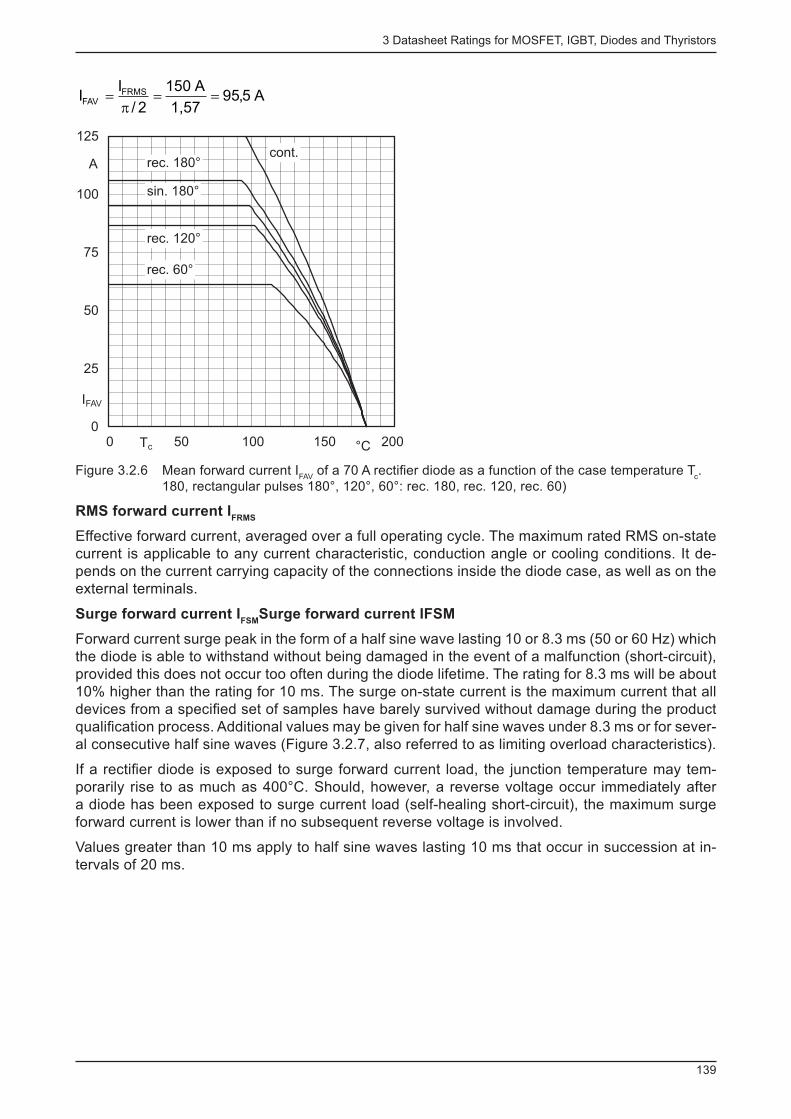
3 Datasheet Ratings for MOSFET, IGBT, Diodes and Thyristors
139
A5,95
1,57
A150
2/
II FRMSFAV ==
p=
0
25
50
75
100
125
T °Cc
IFAV
Acont.
rec. 180°
sin. 180°
rec. 120°
rec. 60°
0 50 100 150 200
Figure 3.2.6 Mean forward current I FAV
of a 70 A rectifi er diode as a function of the case temperature T c .
180, rectangular pulses 180°, 120°, 60°: rec. 180, rec. 120, rec. 60)
RMS forward current I FRMS
Effective forward current, averaged over a full operating cycle. The maximum rated RMS on-state current is applicable to any current characteristic, conduction angle or cooling conditions. It de-pends on the current carrying capacity of the connections inside the diode case, as well as on the external terminals.
Surge forward current I FSM
Surge forward current IFSM
Forward current surge peak in the form of a half sine wave lasting 10 or 8.3 ms (50 or 60 Hz) which the diode is able to withstand without being damaged in the event of a malfunction (short-circuit), provided this does not occur too often during the diode lifetime. The rating for 8.3 ms will be about 10% higher than the rating for 10 ms. The surge on-state current is the maximum current that all devices from a specifi ed set of samples have barely survived without damage during the product qualifi cation process. Additional values may be given for half sine waves under 8.3 ms or for sever-al consecutive half sine waves (Figure 3.2.7, also referred to as limiting overload characteristics).
If a rectifi er diode is exposed to surge forward current load, the junction temperature may tem-porarily rise to as much as 400°C. Should, however, a reverse voltage occur immediately after a diode has been exposed to surge current load (self-healing short-circuit), the maximum surge forward current is lower than if no subsequent reverse voltage is involved.
Values greater than 10 ms apply to half sine waves lasting 10 ms that occur in succession at in-tervals of 20 ms.

3 Datasheet Ratings for MOSFET, IGBT, Diodes and Thyristors
140
0.4
0.6
0.8
1
1.2
1.4
1.6
1,8
2
mst
IF(OV)
IFSM
I = 1150 AFSM(25°C)
I = 1000 AFSM(180°C)
RRM
RRM
RRM
V1
V5.0
V0
×
×
×
1 10 100 1000
Figure 3.2.7 Overcurrents I F(OV)
permissible in the event of malfunction of a 70 A diode in relation to a surge forward current I
FSM lasting 10 ms under different reverse voltage conditions directly
following the last half sine wave; shown over time t.- 0 • V
RRM : no repetitive peak reverse voltage involved,
- ½ • V RRM
: half load of the permissible repetitive peak reverse voltage,- 1 • V
RRM : full load of permissible repetitive peak reverse voltage.
Peak load integral i²t
Reference parameter used to select fuses required for short-circuit protection (also see chapter 4.4). The peak load integral is calculated from the surge forward current I
FSM as follows:
2
tIdti hw2
FSM
t
0
2
FS
hw
×=ò
t hw
stands for the duration of the half sine wave under I FSM
. Consequently, t hw
/2 = 0.005 s at 50 Hz. At frequencies of 50 or 60 Hz, i²t is almost identical, since I
FSM , which is 10% higher at 60 Hz, is
offset by the shorter t hw
: 1.1² · 8.3 ≈ 10.
Non-repetitive peak reverse power dissipation P RSM
(for avalanche rectifi er diodes)
Maximum instantaneous value for power dissipation caused by a non-repetitive reverse current pulse. This value is given as a function of the pulse duration at a virtual junction temperature which corresponds to 80% of the mean forward current permissible at specifi ed cooling and operating conditions (Figure 3.2.8).
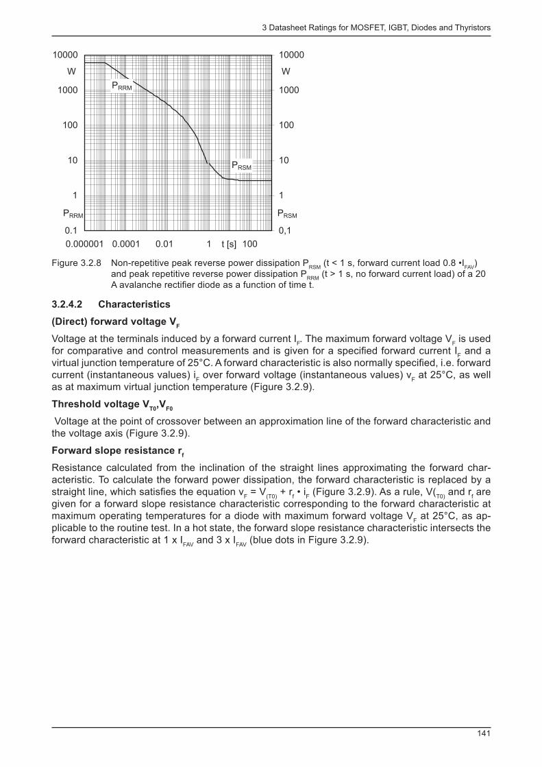
3 Datasheet Ratings for MOSFET, IGBT, Diodes and Thyristors
141
0.1
1
10
100
1000
10000
0.000001 0.0001 0.01 1 100
0,1
1
10
100
1000
10000
t [s]
PRRM
W
PRRM
PRSM
W
PRSM
Figure 3.2.8 Non-repetitive peak reverse power dissipation P RSM
(t < 1 s, forward current load 0.8 •I FAV
) and peak repetitive reverse power dissipation P
RRM (t > 1 s, no forward current load) of a 20
A avalanche rectifi er diode as a function of time t.
3.2.4.2 Characteristics
(Direct) forward voltage V F
Voltage at the terminals induced by a forward current I F . The maximum forward voltage V
F is used
for comparative and control measurements and is given for a specifi ed forward current I F and a
virtual junction temperature of 25°C. A forward characteristic is also normally specifi ed, i.e. forward current (instantaneous values) i
F over forward voltage (instantaneous values) v
F at 25°C, as well
as at maximum virtual junction temperature (Figure 3.2.9).
Threshold voltage V T0
,V F0
Voltage at the point of crossover between an approximation line of the forward characteristic and the voltage axis (Figure 3.2.9).
Forward slope resistance r f
Resistance calculated from the inclination of the straight lines approximating the forward char-acteristic. To calculate the forward power dissipation, the forward characteristic is replaced by a straight line, which satisfi es the equation v
F = V
(T0) + r
f • i
F (Figure 3.2.9). As a rule, V(
T0) and r
f are
given for a forward slope resistance characteristic corresponding to the forward characteristic at maximum operating temperatures for a diode with maximum forward voltage V
F at 25°C, as ap-
plicable to the routine test. In a hot state, the forward slope resistance characteristic intersects the forward characteristic at 1 x I
FAV and 3 x I
FAV (blue dots in Figure 3.2.9).
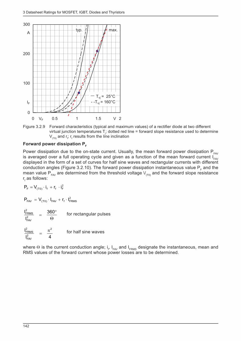
3 Datasheet Ratings for MOSFET, IGBT, Diodes and Thyristors
142
0
100
200
300
0 0.5 1 1.5 2VF V
IF
Amax.typ.
__T = 25°Cvj
- -T = 160°Cvj
Figure 3.2.9 Forward characteristics (typical and maximum values) of a rectifi er diode at two different virtual junction temperatures T
j ; dotted red line = forward slope resistance used to determine
V (T0)
and r f ; r
f results from the line inclination
Forward power dissipation P F
Power dissipation due to the on-state current. Usually, the mean forward power dissipation P FAV
is averaged over a full operating cycle and given as a function of the mean forward current I
FAV
displayed in the form of a set of curves for half sine waves and rectangular currents with different conduction angles (Figure 3.2.10). The forward power dissipation instantaneous value P
F and the
mean value P FAV
are determined from the threshold voltage \/ (T0)
and the forward slope resistance r
f as follows:
2
Fff)0T(F iriVP ×+×=
2
FRMSfFAV)0T(FAV IrIVP ×+×=
Q
°=
360
I
I2
FAV
2
FRMS for rectangular pulses
4I
I 2
2
FAV
2
FRMS p= for half sine waves
where Θ is the current conduction angle; i f , I
FAV and I
FRMS designate the instantaneous, mean and
RMS values of the forward current whose power losses are to be determined.

3 Datasheet Ratings for MOSFET, IGBT, Diodes and Thyristors
143
0
50
100
150
200
0
sin.
180
rec.
180
cont.
IFAV A
W
PFAV
rec.
120
rec.
60
25 50 75 100 125
Figure 3.2.10 Mean forward power dissipation P FAV
over mean forward current I FAV
of a 70 A diode for pure direct current (cont.), half sine waves 180° (sin. 180) and rectangular current pulses 60° (rec. 60) to 180° (rec. 180)
Recovered charge Q rr
Total charge which fl ows from the diode to the outer circuit after having switched over from a de-fi ned forward current load to a defi ned reverse current load. The recovered charge depends on the rate of fall of the decaying current -di
F /dt, the mean forward current I
FM effective at the point of
switching and the virtual junction temperature (Figure 3.2.11).
Peak reverse recovery current I RRM
Reverse current peak after passing over from forward to reverse current load (applies to circuits with unimpeded current decay) (Figure 3.2.11). The maximum possible peak reverse recovery current can be calculated from the recovered charge Q
rr and the current fall rate -di
F /dt using the
following equation (Q f → 0):
÷øö
çèæ-××£
dt
diQ2I F
rrRRM
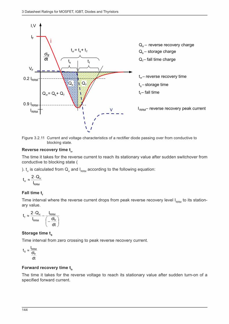
3 Datasheet Ratings for MOSFET, IGBT, Diodes and Thyristors
144
trr= ts+ t f
ts tf
diFdt
F
dt
IRRM
IF
0.9 IRRM
0.2 IRRM
Qs Q f
Qrr= Qs+ Q f
i
v
Qrr – reverse recovery charge
Qs – storage charge
trr– reverse recovery time
ts– storage time
Q f– fall time charge
tf– fall time
IRRM– reverse recovery peak current
VF
I,V
Figure 3.2.11 Current and voltage characteristics of a rectifi er diode passing over from conductive to blocking state.
Reverse recovery time t rr
The time it takes for the reverse current to reach its stationary value after sudden switchover from conductive to blocking state (
). t rr is calculated from Q
rr and I
RRM according to the following equation:
RRM
rrrr
I
Q2t
×»
Fall time t f
Time interval where the reverse current drops from peak reverse recovery level I RRM
to its station-ary value.
÷øö
çèæ-
-×
»
dt
di
I
I
Q2t
F
RRM
RRM
rrf
Storage time t S
Time interval from zero crossing to peak reverse recovery current.
dt
di
It
F
RRMS »
Forward recovery time t fr
The time it takes for the reverse voltage to reach its stationary value after sudden turn-on of a specifi ed forward current.
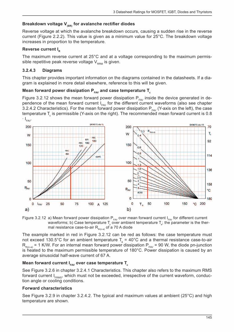
3 Datasheet Ratings for MOSFET, IGBT, Diodes and Thyristors
145
Breakdown voltage V (BR)
for avalanche rectifi er diodes
Reverse voltage at which the avalanche breakdown occurs, causing a sudden rise in the reverse current (Figure 2.2.2). This value is given as a minimum value for 25°C. The breakdown voltage increases in proportion to the temperature.
Reverse current I R
The maximum reverse current at 25°C and at a voltage corresponding to the maximum permis-sible repetitive peak reverse voltage V
RRM is given.
3.2.4.3 Diagrams
This chapter provides important information on the diagrams contained in the datasheets. If a dia-gram is explained in more detail elsewhere, reference to this will be given.
Mean forward power dissipation P FAV
and case temperature T c
Figure 3.2.12 shows the mean forward power dissipation P FAV
inside the device generated in de-pendence of the mean forward current I
FAV for the different current waveforms (also see chapter
3.2.4.2 Characteristics). For the mean forward power dissipation P FAV
(Y-axis on the left), the case temperature T
c is permissible (Y-axis on the right). The recommended mean forward current is 0.8
· I FAV
.
Figure 3.2.12 a) Mean forward power dissipation P FAV
over mean forward current I FAV
for different current waveforms; b) Case temperature T
c over ambient temperature T
a ; the parameter is the ther-
mal resistance case-to-air R th(c-a)
of a 70 A diode
The example marked in red in Figure 3.2.12 can be red as follows: the case temperature must not exceed 130.5°C for an ambient temperature T
a = 40°C and a thermal resistance case-to-air
R th(c-a)
= 1 K/W. For an internal mean forward power dissipation P FAV
= 90 W, the diode pn-junction is heated to the maximum permissible temperature of 180°C. Power dissipation is caused by an average sinusoidal half-wave current of 67 A.
Mean forward current I FAV
over case temperature T c
See Figure 3.2.6 in chapter 3.2.4.1 Characteristics. This chapter also refers to the maximum RMS forward current I
FRMS , which must not be exceeded, irrespective of the current waveform, conduc-
tion angle or cooling conditions.
Forward characteristics
See Figure 3.2.9 in chapter 3.2.4.2. The typical and maximum values at ambient (25°C) and high temperature are shown.
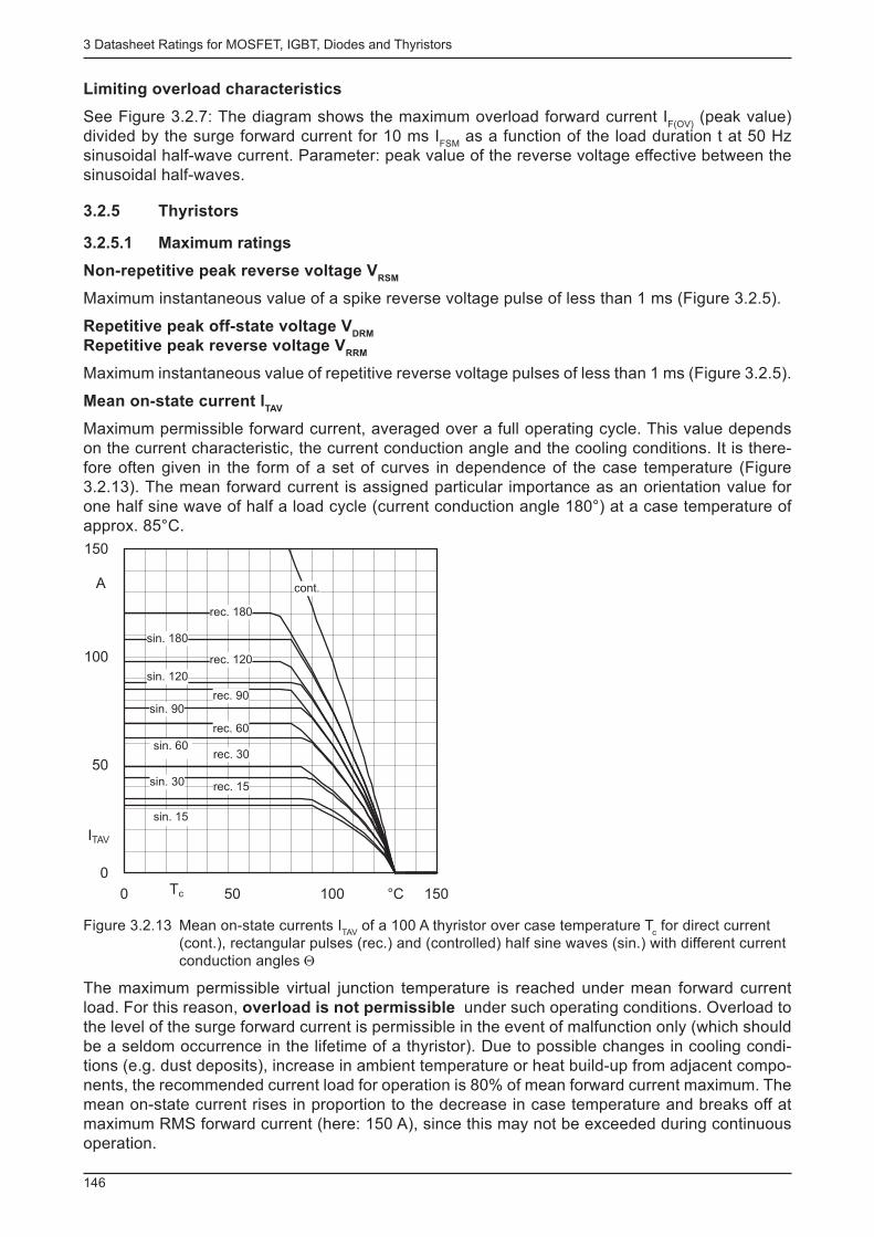
3 Datasheet Ratings for MOSFET, IGBT, Diodes and Thyristors
146
Limiting overload characteristics
See Figure 3.2.7: The diagram shows the maximum overload forward current I F(OV)
(peak value) divided by the surge forward current for 10 ms I
FSM as a function of the load duration t at 50 Hz
sinusoidal half-wave current. Parameter: peak value of the reverse voltage effective between the sinusoidal half-waves.
3.2.5 Thyristors
3.2.5.1 Maximum ratings
Non-repetitive peak reverse voltage V RSM
Maximum instantaneous value of a spike reverse voltage pulse of less than 1 ms (Figure 3.2.5).
Repetitive peak off-state voltage V DRM
Repetitive peak reverse voltage V RRM
Maximum instantaneous value of repetitive reverse voltage pulses of less than 1 ms (Figure 3.2.5).
Mean on-state current l TAV
Maximum permissible forward current, averaged over a full operating cycle. This value depends on the current characteristic, the current conduction angle and the cooling conditions. It is there-fore often given in the form of a set of curves in dependence of the case temperature (Figure 3.2.13). The mean forward current is assigned particular importance as an orientation value for one half sine wave of half a load cycle (current conduction angle 180°) at a case temperature of approx. 85°C.
0
50
100
150
0 Tc °C
ITAV
A cont.
rec. 180
sin. 180
rec. 120
rec. 30
rec. 15
rec. 90
rec. 60
sin. 120
sin. 90
sin. 60
sin. 30
sin. 15
50 100 150
Figure 3.2.13 Mean on-state currents I TAV
of a 100 A thyristor over case temperature T c for direct current
(cont.), rectangular pulses (rec.) and (controlled) half sine waves (sin.) with different current conduction angles Θ
The maximum permissible virtual junction temperature is reached under mean forward current load. For this reason, overload is not permissible under such operating conditions. Overload to the level of the surge forward current is permissible in the event of malfunction only (which should be a seldom occurrence in the lifetime of a thyristor). Due to possible changes in cooling condi-tions (e.g. dust deposits), increase in ambient temperature or heat build-up from adjacent compo-nents, the recommended current load for operation is 80% of mean forward current maximum. The mean on-state current rises in proportion to the decrease in case temperature and breaks off at maximum RMS forward current (here: 150 A), since this may not be exceeded during continuous operation.
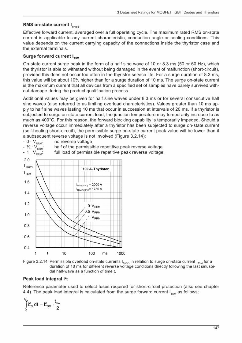
3 Datasheet Ratings for MOSFET, IGBT, Diodes and Thyristors
147
RMS on-state current I TRMS
Effective forward current, averaged over a full operating cycle. The maximum rated RMS on-state current is applicable to any current characteristic, conduction angle or cooling conditions. This value depends on the current carrying capacity of the connections inside the thyristor case and the external terminals.
Surge forward current I TSM
On-state current surge peak in the form of a half sine wave of 10 or 8.3 ms (50 or 60 Hz), which the thyristor is able to withstand without being damaged in the event of malfunction (short-circuit), provided this does not occur too often in the thyristor service life. For a surge duration of 8.3 ms, this value will be about 10% higher than for a surge duration of 10 ms. The surge on-state current is the maximum current that all devices from a specifi ed set of samples have barely survived with-out damage during the product qualifi cation process.
Additional values may be given for half sine waves under 8.3 ms or for several consecutive half sine waves (also referred to as limiting overload characteristics). Values greater than 10 ms ap-ply to half sine waves lasting 10 ms that occur in succession at intervals of 20 ms. If a thyristor is subjected to surge on-state current load, the junction temperature may temporarily increase to as much as 400°C. For this reason, the forward blocking capability is temporarily impeded. Should a reverse voltage occur immediately after a thyristor has been subjected to surge on-state current (self-healing short-circuit), the permissible surge on-state current peak value will be lower than if a subsequent reverse voltage is not involved (Figure 3.2.14): - 0 · V
RRM : no reverse voltage
- ½ · V RRM
: half of the permissible repetitive peak reverse voltage - 1 · V
RRM : full load of permissible repetitive peak reverse voltage.
0.4
0.6
0.8
1.0
1.2
1.4
1.6
1,8
2.0
1 10 100 1000mst
IT(OV)
ITSM
ITSM(25°C) = 2000 A
ITSM(130°C)= 1750 A
0 ×VRRM
0.5 ×VRRM
1 ×VRRM
100 A-Thyristor
Figure 3.2.14 Permissible overload on-state currents I T(OV)
in relation to surge on-state current I TSM
for a duration of 10 ms for different reverse voltage conditions directly following the last sinusoi-dal half-wave as a function of time t.
Peak load integral i²t
Reference parameter used to select fuses required for short-circuit protection (also see chapter 4.4). The peak load integral is calculated from the surge forward current I
TSM as follows:
2
tIdti hw2
TSM
t
0
2
TS
hw
×=ò
3 Datasheet Ratings for MOSFET, IGBT, Diodes and Thyristors
148
Here, t hw
stands for the duration of the half sine wave under I TSM
gilt. Consequently, t hw
/2 = 0.005 s at 50 Hz. At frequencies of 50 Hz or 60 Hz, i²t is almost identical, since l
TSM , which is 10% higher
at 60 Hz, is offset by the shorter t hw
: 1.1² · 8.3 ≈ 10.
Critical rate of rise of on-state current (di/dt) cr
Maximum rate of rise of on-state current which the thyristor is able to withstand without being da-maged. This depends on the operating frequency, the peak on-state current, the off-state voltage directly before thyristor fi ring, as well as on the size and rate of rise of the gate pulses. What must also be taken into account is the fact that the thyristor is loaded with a high discharge current at turn-on induced by an RC-snubber connected in parallel to the thyristor for overvoltage protection.
The values given apply to frequencies of 50 to 60 Hz, a current amplitude which is three times the mean on-state current (for half sine waves at a case temperature of 85°C) and gate pulses of fi ve times the gate trigger current with a rising edge of at least 1 A/µs without RC snubber. The critical di/dt rises at lower current amplitude and temperature and falls at low or slow-rising gate trigger current and higher repetition frequency. Amplifying gate thyristors can reach very high (di/dt)
cr val-
ues (also see chapter 2.2.2.4).
Peak gate power dissipation P GM
Maximum permissible power dissipation caused by the thyristor gate current. It depends on the gate pulse duration (Figure 3.2.21).
Average gate power dissipation P GAV
Maximum permissible power dissipation caused by the thyristor gate current, averaged over a full operating cycle.
For temperature limits see chapter 3.2.1 "Temperatures".
3.2.5.2 Characteristics
On-state voltage V T
Voltage at the main terminals induced by a forward on-state current I T . The maximum forward
voltage V T is used for comparative and control measurements and is given for a specifi ed forward
current l T and a virtual junction temperature of 25°C. The maximum on-state voltage v
T is used for
comparative and control measurements and is given for a specifi ed on-state current i T at 25°C as
well as at the maximum virtual junction temperature (Figure 3.2.15).
Threshold voltage V T(T0)
Voltage at the point of crossover between an approximation line of the forward characteristic and the voltage axis (Figure 3.2.15).
On-state slope resistance r T On-state slope resistance rT
Resistance calculated from the inclination of the straight lines approximating the forward charac-teristic (Figure 3.2.15). To calculate the on-state power dissipation, the on-state characteristic is replaced by a straight-line which is determined from v
T = V
T(T0) + r
T · i
T . As a rule, V
T(T0) and r
T are
given for an on-state slope resistance characteristic which corresponds to the on-state charac-teristic at the maximum virtual junction temperature for a thyristor whose on-state voltage V
T has
its maximum value as applicable to the routine test at at 25°C. In a hot state, the forward slope resistance characteristic intersects the forward characteristic at 1 x I
FAV and 3 x I
FAV (blue dots in
Figure 3.2.15).
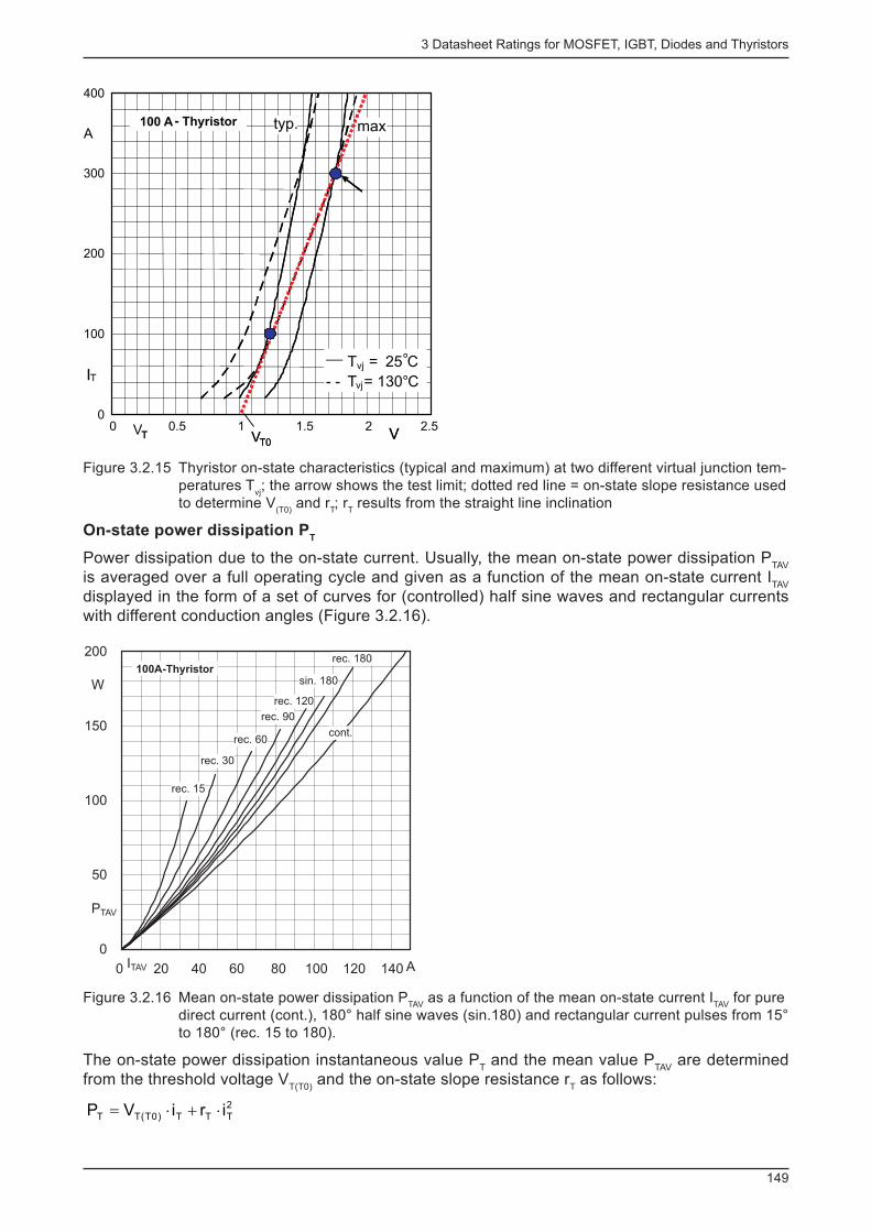
3 Datasheet Ratings for MOSFET, IGBT, Diodes and Thyristors
149
0
200
300
400
0 0.5 1 1.5 2 2.5VT V
IT
.
Tvj = 25 °C
- -Tvj= 130 °C
-Thyristor
VT0
100
T V
IT
Amaxtyp.
Tvj = 25°C
- - Tvj= 130°C
100 A- Thyristor
VT0
___
Figure 3.2.15 Thyristor on-state characteristics (typical and maximum) at two different virtual junction tem-peratures T
vj ; the arrow shows the test limit; dotted red line = on-state slope resistance used
to determine V (T0)
and r T ; r
T results from the straight line inclination
On-state power dissipation P T
Power dissipation due to the on-state current. Usually, the mean on-state power dissipation P TAV
is averaged over a full operating cycle and given as a function of the mean on-state current I
TAV
displayed in the form of a set of curves for (controlled) half sine waves and rectangular currents with different conduction angles (Figure 3.2.16).
0
50
100
150
200
0 20 40 60 80 100 120 140
rec. 15
rec. 30
rec. 60
rec. 90
rec. 120
sin. 180
rec. 180
cont.
ITAV A
W
PTAV
100A-Thyristor
Figure 3.2.16 Mean on-state power dissipation P TAV
as a function of the mean on-state current I TAV
for pure direct current (cont.), 180° half sine waves (sin.180) and rectangular current pulses from 15° to 180° (rec. 15 to 180).
The on-state power dissipation instantaneous value P T and the mean value P
TAV are determined
from the threshold voltage V T(T0)
and the on-state slope resistance r T as follows:
2
TTT)0T(TT iriVP ×+×=
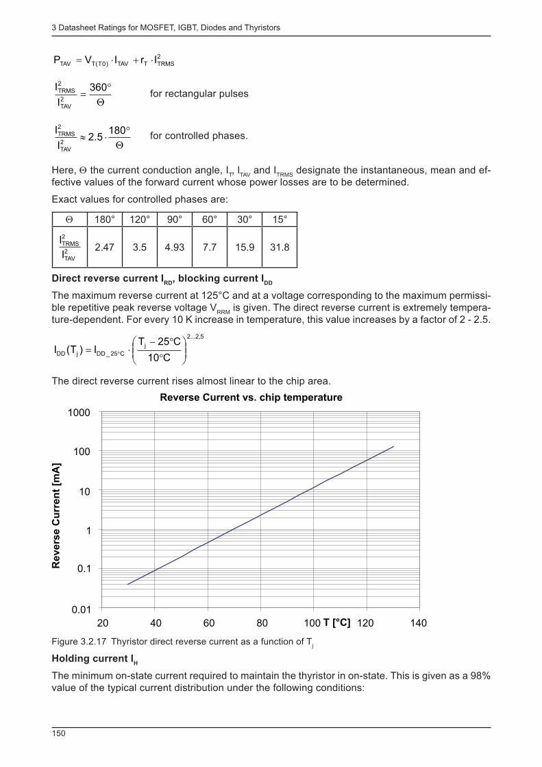
3 Datasheet Ratings for MOSFET, IGBT, Diodes and Thyristors
150
2
TRMSTTAV)0T(TTAV IrIVP ×+×=
Q
°=
360
I
I2
TAV
2
TRMS for rectangular pulses
Q
°×»180
5.2I
I2
TAV
2
TRMS for controlled phases.
Here, Θ the current conduction angle, I T , l
TAV and I
TRMS designate the instantaneous, mean and ef-
fective values of the forward current whose power losses are to be determined.
Exact values for controlled phases are:
Θ 180° 120° 90° 60° 30° 15°
2
TAV
2
TRMS
I
I 2.47 3.5 4.93 7.7 15.9 31.8
Direct reverse current I RD
, blocking current I DD
The maximum reverse current at 125°C and at a voltage corresponding to the maximum permissi-ble repetitive peak reverse voltage V
RRM is given. The direct reverse current is extremely tempera-
ture-dependent. For every 10 K increase in temperature, this value increases by a factor of 2 - 2.5.
5,2...2
j
C25_DDjDDC10
C25TI)T(I ÷÷
ø
öççè
æ°
°-×= °
The direct reverse current rises almost linear to the chip area.
Reverse Current vs. chip temperature
0.01
0.1
1
10
100
1000
20 40 60 80 100 120 140T [°C]
Revers
e C
urr
en
t [m
A]
Figure 3.2.17 Thyristor direct reverse current as a function of T j
Holding current I H
The minimum on-state current required to maintain the thyristor in on-state. This is given as a 98% value of the typical current distribution under the following conditions:
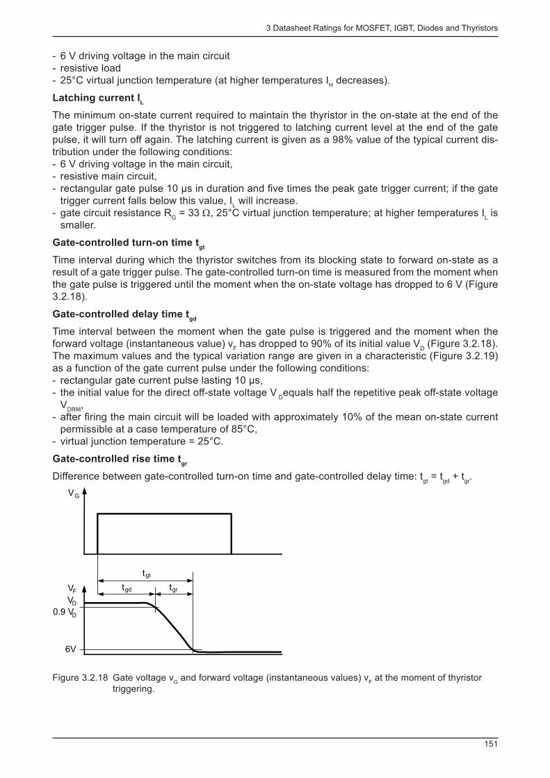
3 Datasheet Ratings for MOSFET, IGBT, Diodes and Thyristors
151
- 6 V driving voltage in the main circuit - resistive load - 25°C virtual junction temperature (at higher temperatures I
H decreases).
Latching current I L
The minimum on-state current required to maintain the thyristor in the on-state at the end of the gate trigger pulse. If the thyristor is not triggered to latching current level at the end of the gate pulse, it will turn off again. The latching current is given as a 98% value of the typical current dis-tribution under the following conditions: - 6 V driving voltage in the main circuit, - resistive main circuit, - rectangular gate pulse 10 µs in duration and fi ve times the peak gate trigger current; if the gate trigger current falls below this value, I
L will increase.
- gate circuit resistance R G = 33 Ω, 25°C virtual junction temperature; at higher temperatures I
L is
smaller.
Gate-controlled turn-on time t gt
Time interval during which the thyristor switches from its blocking state to forward on-state as a result of a gate trigger pulse. The gate-controlled turn-on time is measured from the moment when the gate pulse is triggered until the moment when the on-state voltage has dropped to 6 V (Figure 3.2.18).
Gate-controlled delay time t gd
Time interval between the moment when the gate pulse is triggered and the moment when the forward voltage (instantaneous value) v
F has dropped to 90% of its initial value V
D (Figure 3.2.18).
The maximum values and the typical variation range are given in a characteristic (Figure 3.2.19) as a function of the gate current pulse under the following conditions: - rectangular gate current pulse lasting 10 µs, - the initial value for the direct off-state voltage V
D equals half the repetitive peak off-state voltage
V DRM
, - after fi ring the main circuit will be loaded with approximately 10% of the mean on-state current permissible at a case temperature of 85°C,
- virtual junction temperature = 25°C.
Gate-controlled rise time t gr
Difference between gate-controlled turn-on time and gate-controlled delay time: t gt = t
gd + t
gr .
t
t
VG
VF
VD
0.9 VD
6V
tgt
tgd tgr
Figure 3.2.18 Gate voltage v G and forward voltage (instantaneous values) v
F at the moment of thyristor
triggering.

3 Datasheet Ratings for MOSFET, IGBT, Diodes and Thyristors
152
0.1
1
10
100
1000
0.01 0.1 1 10 100
100 A-Thyristor
tgd
[µs]
IG [A]
Figure 3.2.19 Typical dependency of a thyristor gate-controlled delay time t gd
on gate current I G ; the
shaded area represents the variation range. Recovered charge Q
rr
Peak reverse recovery current I RRM
Reverse recovery time t rr
Fall time t f
Repetitive peak off-state current I DRM
Maximum rated value at the maximum permissible repetitive peak off-state voltage at 25°C.
Gate trigger voltage V GT
and gate trigger current I GT
Minimum gate current and gate voltage required to ensure that each thyristor of the given type is triggered (Figure 3.2.21). These parameters are subject to the following conditions: - ≥6 V driving voltage in the main circuit, - resistive main circuit, - rectangular gate current pulse of at least 100 µs, - virtual junction temperature = 25°C.
Gate pulses under 100 µs will effect an increase in the minimum gate trigger current and voltage values by a factor of 1.4 to 2. The driver unit should ensure that the trigger current value given in the datasheet is exceeded by a factor of four or even fi ve.
As for amplifying gate thyristors, a high rate of rise in the main current will provoke a temporary counter voltage at the gate terminal as a consequence of the voltage spread across the thyristor chip layers. In the case of insuffi cient driving voltage or too high a driver output resistance, the temporary counter voltage may suppress or even temporarily reverse the gate current (Figure 3.2.20). This may damage the thyristor. The driver dimensioning must therefore comply with the power requirements.
See chapter 3.2.4.2 Rectifi er diode characteristics and Figure 3.2.11 .
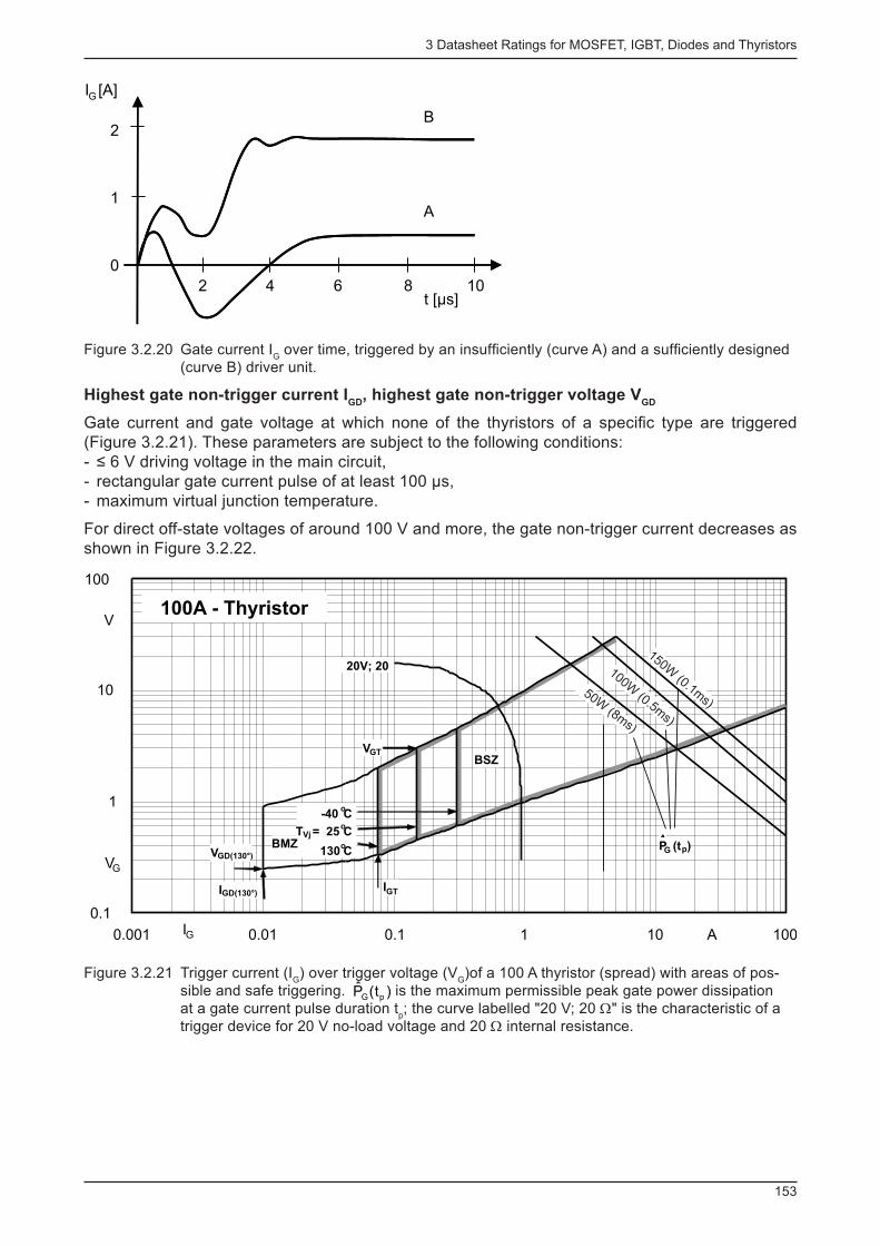
3 Datasheet Ratings for MOSFET, IGBT, Diodes and Thyristors
153
IG [A]
t [µs]2 4 6 8 10
0
1
2B
A
Figure 3.2.20 Gate current I G over time, triggered by an insuffi ciently (curve A) and a suffi ciently designed
(curve B) driver unit.
Highest gate non-trigger current I GD
, highest gate non-trigger voltage V GD
Gate current and gate voltage at which none of the thyristors of a specifi c type are triggered (Figure 3.2.21). These parameters are subject to the following conditions: - ≤ 6 V driving voltage in the main circuit, - rectangular gate current pulse of at least 100 µs, - maximum virtual junction temperature.
For direct off-state voltages of around 100 V and more, the gate non-trigger current decreases as shown in Figure 3.2.22.
0.1
1
10
100
0.001 0.01 0.1 1 10 100IG A
VG
V
VGD(130°)
VGT
IGTIGD(130°)
-40oC
TVj = 25oC
130oC
20V; 20
BSZ
BMZ ^PG (tp)
100A - Thyristor
50W(8m
s)
100W(0.5m
s)
150W(0.1m
s)
Figure 3.2.21 Trigger current (I G ) over trigger voltage (V
G )of a 100 A thyristor (spread) with areas of pos-
sible and safe triggering. )t(P pGis the maximum permissible peak gate power dissipation
at a gate current pulse duration t p ; the curve labelled "20 V; 20 Ω" is the characteristic of a
trigger device for 20 V no-load voltage and 20 Ω internal resistance.
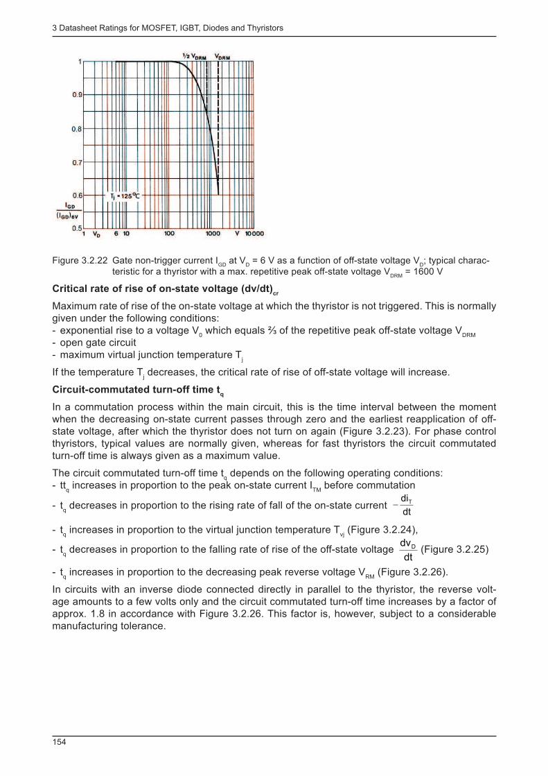
3 Datasheet Ratings for MOSFET, IGBT, Diodes and Thyristors
154
Figure 3.2.22 Gate non-trigger current I GD
at V D = 6 V as a function of off-state voltage V
D ; typical charac-
teristic for a thyristor with a max. repetitive peak off-state voltage V DRM
= 1600 V
Critical rate of rise of on-state voltage (dv/dt) cr
Maximum rate of rise of the on-state voltage at which the thyristor is not triggered. This is normally given under the following conditions: - exponential rise to a voltage V
0 which equals ⅔ of the repetitive peak off-state voltage V
DRM
- open gate circuit - maximum virtual junction temperature T
j
If the temperature T j decreases, the critical rate of rise of off-state voltage will increase.
Circuit-commutated turn-off time t q
In a commutation process within the main circuit, this is the time interval between the moment when the decreasing on-state current passes through zero and the earliest reapplication of off-state voltage, after which the thyristor does not turn on again (Figure 3.2.23). For phase control thyristors, typical values are normally given, whereas for fast thyristors the circuit commutated turn-off time is always given as a maximum value.
The circuit commutated turn-off time t q depends on the following operating conditions:
- t t q increases in proportion to the peak on-state current I
TM before commutation
- t q decreases in proportion to the rising rate of fall of the on-state current
dt
diT-
- t q increases in proportion to the virtual junction temperature T
vj (Figure 3.2.24),
- t q decreases in proportion to the falling rate of rise of the off-state voltage
dt
dvD (Figure 3.2.25)
- t q increases in proportion to the decreasing peak reverse voltage V
RM (Figure 3.2.26).
In circuits with an inverse diode connected directly in parallel to the thyristor, the reverse volt-age amounts to a few volts only and the circuit commutated turn-off time increases by a factor of approx. 1.8 in accordance with Figure 3.2.26. This factor is, however, subject to a considerable manufacturing tolerance.
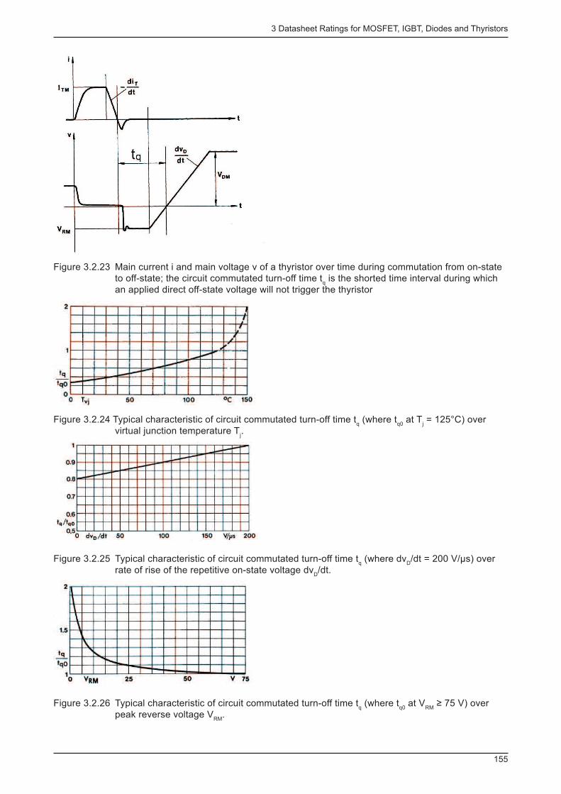
3 Datasheet Ratings for MOSFET, IGBT, Diodes and Thyristors
155
Figure 3.2.23 Main current i and main voltage v of a thyristor over time during commutation from on-state to off-state; the circuit commutated turn-off time t
q is the shorted time interval during which
an applied direct off-state voltage will not trigger the thyristor
Figure 3.2.24 Typical characteristic of circuit commutated turn-off time t q (where t
q0 at T
j = 125°C) over
virtual junction temperature T j .
Figure 3.2.25 Typical characteristic of circuit commutated turn-off time t q (where dv
D /dt = 200 V/µs) over
rate of rise of the repetitive on-state voltage dv D /dt.
Figure 3.2.26 Typical characteristic of circuit commutated turn-off time t q (where t
q0 at V
RM ≥ 75 V) over
peak reverse voltage V RM
.
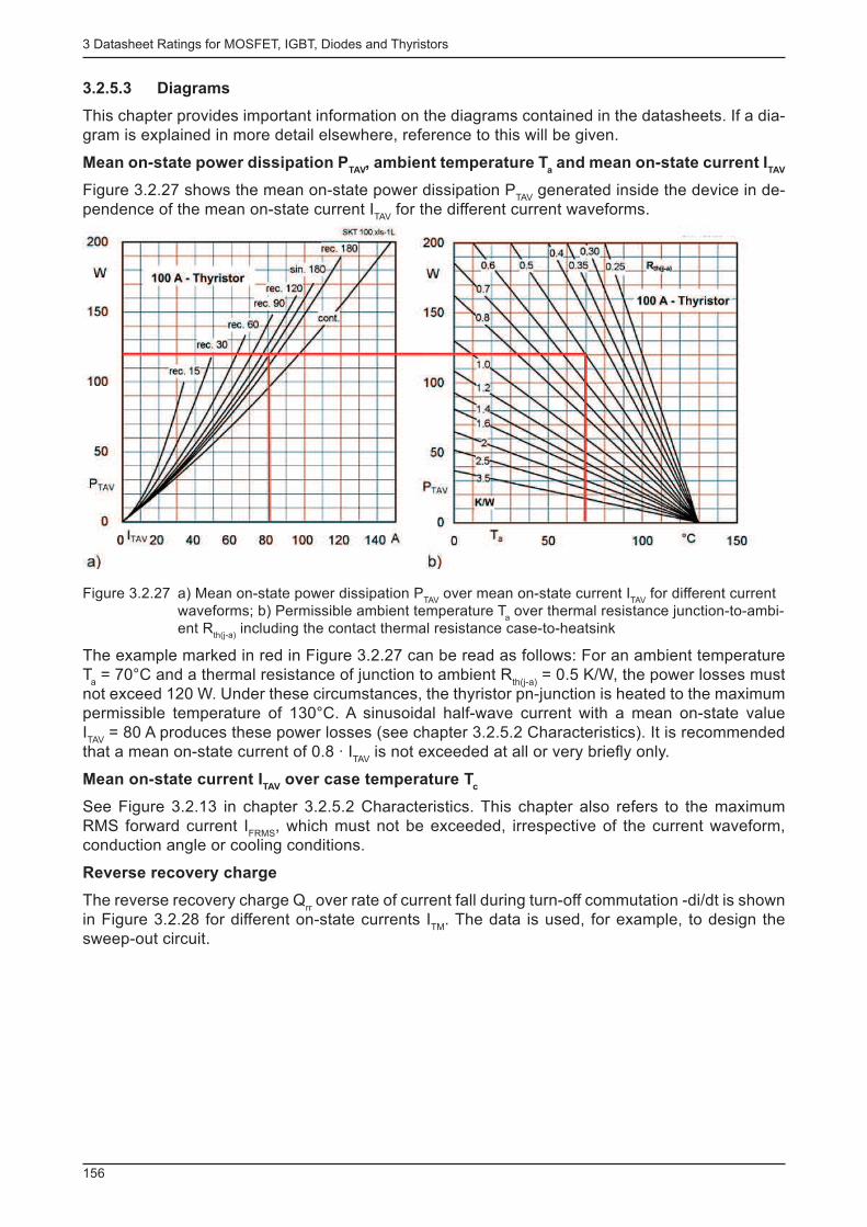
3 Datasheet Ratings for MOSFET, IGBT, Diodes and Thyristors
156
3.2.5.3 Diagrams
This chapter provides important information on the diagrams contained in the datasheets. If a dia-gram is explained in more detail elsewhere, reference to this will be given.
Mean on-state power dissipation P TAV
, ambient temperature T a and mean on-state current I
TAV
Figure 3.2.27 shows the mean on-state power dissipation P TAV
generated inside the device in de-pendence of the mean on-state current I
TAV for the different current waveforms.
Figure 3.2.27 a) Mean on-state power dissipation P TAV
over mean on-state current I TAV
for different current waveforms; b) Permissible ambient temperature T
a over thermal resistance junction-to-ambi-
ent R th(j-a)
including the contact thermal resistance case-to-heatsink
The example marked in red in Figure 3.2.27 can be read as follows: For an ambient temperature T
a = 70°C and a thermal resistance of junction to ambient R
th(j-a) = 0.5 K/W, the power losses must
not exceed 120 W. Under these circumstances, the thyristor pn-junction is heated to the maximum permissible temperature of 130°C. A sinusoidal half-wave current with a mean on-state value I TAV
= 80 A produces these power losses (see chapter 3.2.5.2 Characteristics). It is recommended that a mean on-state current of 0.8 · I
TAV is not exceeded at all or very briefl y only.
Mean on-state current I TAV
over case temperature T c
See Figure 3.2.13 in chapter 3.2.5.2 Characteristics. This chapter also refers to the maximum RMS forward current I
FRMS , which must not be exceeded, irrespective of the current waveform,
conduction angle or cooling conditions.
Reverse recovery charge
The reverse recovery charge Q rr over rate of current fall during turn-off commutation -di/dt is shown
in Figure 3.2.28 for different on-state currents I TM
. The data is used, for example, to design the sweep-out circuit.
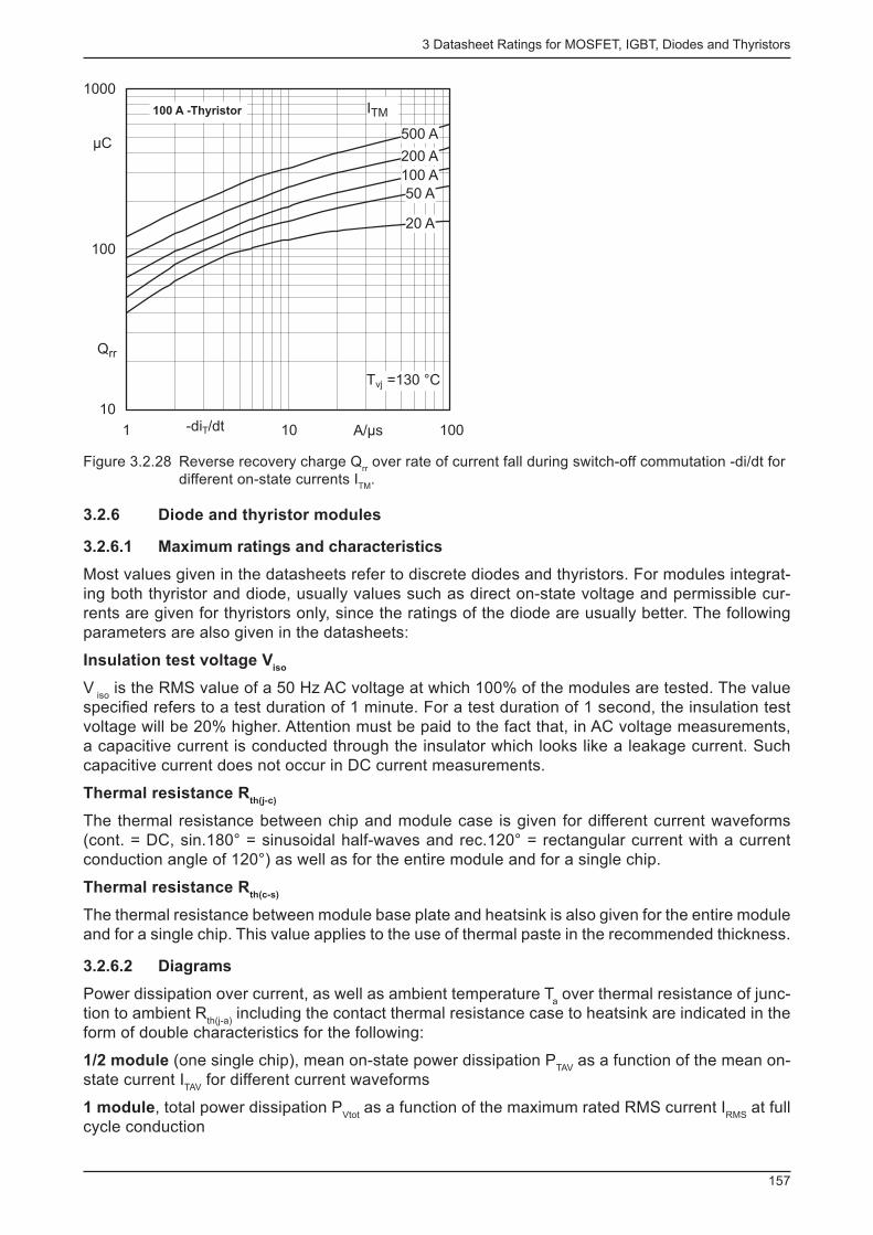
3 Datasheet Ratings for MOSFET, IGBT, Diodes and Thyristors
157
10
100
1000
1 10 100-diT/dt A/µs
Qrr
μC
ITM
20 A
Tvj =130 °C
50 A
100 A
200 A
500 A
100 A -Thyristor
Figure 3.2.28 Reverse recovery charge Q rr over rate of current fall during switch-off commutation -di/dt for
different on-state currents I TM
.
3.2.6 Diode and thyristor modules
3.2.6.1 Maximum ratings and characteristics
Most values given in the datasheets refer to discrete diodes and thyristors. For modules integrat-ing both thyristor and diode, usually values such as direct on-state voltage and permissible cur-rents are given for thyristors only, since the ratings of the diode are usually better. The following parameters are also given in the datasheets:
Insulation test voltage V iso
V iso
is the RMS value of a 50 Hz AC voltage at which 100% of the modules are tested. The value specifi ed refers to a test duration of 1 minute. For a test duration of 1 second, the insulation test voltage will be 20% higher. Attention must be paid to the fact that, in AC voltage measurements, a capacitive current is conducted through the insulator which looks like a leakage current. Such capacitive current does not occur in DC current measurements.
Thermal resistance R th(j-c)
The thermal resistance between chip and module case is given for different current waveforms (cont. = DC, sin.180° = sinusoidal half-waves and rec.120° = rectangular current with a current conduction angle of 120°) as well as for the entire module and for a single chip.
Thermal resistance R th(c-s)
The thermal resistance between module base plate and heatsink is also given for the entire module and for a single chip. This value applies to the use of thermal paste in the recommended thickness.
3.2.6.2 Diagrams
Power dissipation over current, as well as ambient temperature T a over thermal resistance of junc-
tion to ambient R th(j-a)
including the contact thermal resistance case to heatsink are indicated in the form of double characteristics for the following:
1/2 module (one single chip), mean on-state power dissipation P TAV
as a function of the mean on-state current I
TAV for different current waveforms
1 module , total power dissipation P Vtot
as a function of the maximum rated RMS current I RMS
at full cycle conduction
3 Datasheet Ratings for MOSFET, IGBT, Diodes and Thyristors
158
2 modules in a two-pulse bridge circuit (B2), total power dissipation P Vtot
as a function of the maxi-mum direct output current of the complete circuit I
D for resistive load (R) and inductive load (L)
3 modules in a six-pulse bridge circuit (B6) and in a three-phase ac-controller (W3), total power dissipation P
Vtot as a function of the direct current I
D or the maximum rated RMS current per phase
I RMS
.
The diagrams for 1, 2, and 3 modules must be read as follows: For the total power dissipa-
tion P Vtot
(plotted on the left), the permissible case temperature T c (shown on the right) is applica-
ble. All other characteristics correspond to those for discrete diodes and thyristors.
3.3 IGBT modules
When selecting IGBT modules or comparing their properties using datasheet parameters, it must be borne in mind that, owing to the different specifi cation conditions, the values given in the da-tasheets of different semiconductor manufacturers are comparable to a certain extent only. In many cases, owing to the complex, application-specifi c interaction between different module fea-tures, additional measurements will be necessary.
Due to the developments over the past few decades, SEMIKRON datasheets also have differen-ces with regard to datasheet layout, data content and specifi cations for the different generations of IGBT modules and different module designs. Since this data is to be standardised as part our product maintenance measures, the following information essentially refers to the latest data-sheets issued in January 2010, i.e. the latest IGBT4 chip generation is referred to in the context of IGBT modules, cf. Figure 3.3.1. Where applicable, different datasheet structures for the data-sheets of older modules which are still being produced will be pointed out expressly.
In many cases, key data such as maximum ratings and characteristics that is applicable to every different product type withing a certain product range, as well as application notes for SEMIKRON IGBT modules are not included in the product-type-specifi c datasheets. Instead, these are inclu-ded in the "Technical Explanations" of the respective product range, e.g. the notes on safe opera-ting areas detailed in chapter 3.3.4.
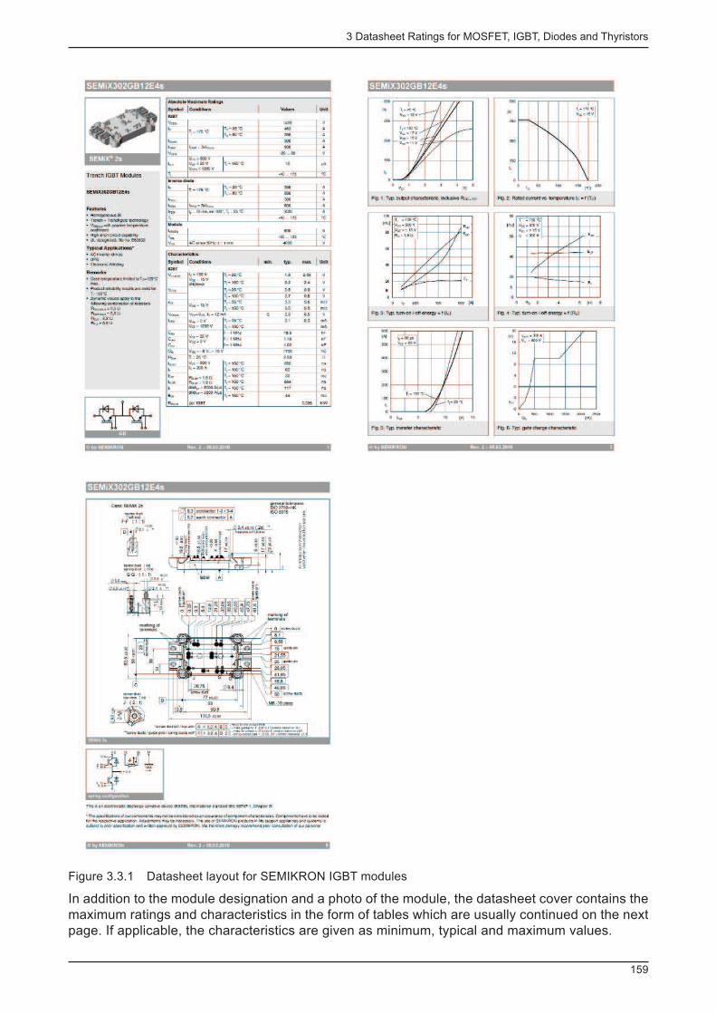
3 Datasheet Ratings for MOSFET, IGBT, Diodes and Thyristors
159
Figure 3.3.1 Datasheet layout for SEMIKRON IGBT modules
In addition to the module designation and a photo of the module, the datasheet cover contains the maximum ratings and characteristics in the form of tables which are usually continued on the next page. If applicable, the characteristics are given as minimum, typical and maximum values.

3 Datasheet Ratings for MOSFET, IGBT, Diodes and Thyristors
160
General information on the module is given under "Features" and "Typical Applications" in the shaded area to the left of the maximum ratings and characteristics. The "Remarks" section con-tains important information that is relevant to the datasheet specifi cations, e.g. operating or mea-surement conditions. This also includes basic diagrams of the internal circuits (e.g. half-bridge GB, chopper module GAL, cf. chapter 2.5.2.7) of the topologies described in the datasheet. The datasheet date of issue is given on all pages in the shaded footer.
The data given in the tables are followed by the diagrams usually comprising two pages. The num-bering of the diagrams [Figure 1…] is based on a general numbering structure, i.e. the diagrams in a datasheet will not necessarily be numbered consecutively. The last page of the datasheet contains the module drawing including dimension data, as well as a basic diagram of the internal circuits showing the terminal layout.
The diode connected directly in parallel to the IGBT is called the inverse diode. The freewheeling diode is positioned in the bridge arm where the IGBT is not. This is of no relevance to half-bridge modules, since the inverse diode of the fi rst IGBT serves as a freewheeling diode for the second IGBT. The freewheeling diode in chopper modules (GAL/GAR), however, may boast higher values than the inverse diode.
3.3.1 Maximum ratings
In the datasheets, the maximum ratings are specifi ed separately for each individual component of an IGBT module (IGBT, diode, case, temperature sensor, if available). All ratings for IGBT and diodes refer to one switch (arm), irrespective of the number of IGBT or diode chips actually con-nected in parallel per switch (arm) in the transistor module.
Absolute Maximum Ratings
Symbol Conditions Values Unit
IGBT
VCES 1200 V
ICTj = 175 °C
Tc = 25 °C 463 A
Tc = 80 °C 356 A
ICnom 300 A
ICRM ICRM = 3xICnom 900 A
VGES -20 ... 20 V
tpsc
VCC = 800 V
VGE ! 20 V
VCES ! 1200 V
Tj = 150 °C 10 µs
Tj -40 ... 175 °C
Inverse diode
IFTj = 175 °C
Tc = 25 °C 356 A
Tc = 80 °C 266 A
IFnom 300 A
IFRM IFRM = 3xIFnom 900 A
IFSM tp = 10 ms, sin 180°, Tj = 25 °C 1620 A
Tj -40 ... 175 °C
Module
It(RMS) 600 A
Tstg -40 ... 125 °C
Visol AC sinus 50Hz, t = 1 min 4000 V
Figure 3.3.2 Datasheet excerpt: maximum ratings of an IGBT module
3.3.1.1 IGBT maximum ratings
Collector-emitter voltage V CES
Maximum voltage between the collector and emitter terminals of the IGBT chips with gate-emitter short-circuited; parameters: chip temperature T
j = 25°C. The maximum collector-emitter voltage decreas-
es in proportion to the temperature owing to the temperature dependency of the breakdown voltage. Irrespective of the load conditions, the sum of the collector-emitter supply voltage V
CC and the
switching overvoltage ∆V CE
= L σ · di
C /dt must not exceed voltage V
CES (L
σ : sum of the parasitic in-
ductance in the commutation circuit), cf. chapter 5.1.
3 Datasheet Ratings for MOSFET, IGBT, Diodes and Thyristors
161
Continuous collector current I C
Maximum permissible continuous direct current over the collector output at which the permissible chip temperature is reached. Parameter: case temperature T
c = 25°C / 80°C, heatsink tempera-
ture T s = 25°C / 70°C for modules without base plate; for modules which can be soldered in PCBs
(SEMITOP) also maximum PCB temperature at the output terminals; chip temperature T j = T
j(max)
I C for IGBT modules with base plate is determined from
I C = P
tot(max) /V
CE(sat) where P
tot(max) = (T
j(max) – T
c )/R
th(j-c) ,
and for modules without base plate from
I C = P
tot(max) /V
CE(sat) where P
tot(max) = (T
j(max) – T
s )/R
th(j-s) .
Since I C designates a static maximum value, it is not relevant to switching operation.
Nominal chip current I Cnom
Rated current of IGBT chips indicated in the chip manufacturer's datasheet ("Continuous collector current limited by T
j(max) ") multiplied by the number of IGBT chips per switch connected in parallel
in the module.
Repetitive peak collector current I CRM
Peak current value at collector output during pulse operation.
I CRM
corresponds to the peak current indicated in the IGBT chip manufacturer's datasheet ("pulsed collector current limited by T
j(max) ") multiplied by the number of IGBT chips per switch connected in
parallel in the module. This parameter is independent of the pulse duration and must be adhered to, even if the maximum chip temperature is not reached. Otherwise the chip metallisation will be damaged and premature chip ageing will occur. In many datasheets I
CRM is indicated as 2 · I
Cnom ;
this corresponds to the former specifi ed peak collector current I CM
.
For IGBT4 chips (T4, E4) currently used in SEMIKRON IGBT modules, I CRM
is specifi ed as 3 x I Cnom
by the chip manufacturer. For a gate resistance specifi ed at the nominal operating point and a high DC link voltage, it is not always possible to turn these currents off without exceeding the collector-emitter voltage V
CES . As shown in relevant tests, repetitive turn-off of such high currents may cause
early desaturation of the hottest chips and, consequently, involve high power losses. SEMIKRON therefore recommends turning off currents above the admissible value specifi ed for the predeces-sor chip generation with 2 · I
Cnom within RBSOA as an exception only and provided that suitable
countermeasures are taken, e.g. DC link voltage reduction, active clamping, very slow turn-off or turn-off power dissipation reduction. Such action is likely to involve substantial losses which must be taken into account when designing the semiconductor.
Gate-emitter voltage V GES
Maximum voltage between the gate and emitter terminals of the IGBT chips; parameters: case temperature T
c = 25°C
Maximum turn-on time during short-circuit t psc
Maximum duration of desaturation caused by overcurrent or short-circuit at a specifi ed supply volt-age, collector-emitter voltage and chip temperature; parameters: collector-emitter supply voltage V
CC , maximum gate-emitter voltage V
GE , maximum collector-emitter voltage V
CES , chip temperature
T j (for the latest Infi neon chips < T
j(max) ).
Operating temperature range T j ; T
j(min) ....T
j(max)
Permissible IGBT chip temperature within which the IGBT module may be operated; especially under permanent load the chip temperature should be kept at least 25 K below T
j(max) .
3 Datasheet Ratings for MOSFET, IGBT, Diodes and Thyristors
162
3.3.1.2 Maximum ratings of integrated inverse diodes (freewheeling diodes)
Inverse diode forward current I F
Maximum rated direct reverse current at collector output; parameters: case temperature T c =
25°C / 80°C, heatsink temperature T s = 25°C / 70°C for modules without base plate; also maximum
PCB temperature at the output terminals of modules which can be soldered onto PCBs (SEMI-TOP); chip temperature T
j = T
j(max)
Nominal diode chip current I Fnom
Rated current of the diode chips used as indicated in the chip manufacturer's datasheet ("Continu-ous direct current (diode) limited by T
j(max) ") multiplied by the number of chips connected in parallel
in the module per switch.
Repetitive peak forward current of the inverse diode I FRM
Today's SEMIKRON modules feature I FRM
= 3 · I Fnom
, where I Fnom
is the rated current of the chips used as indicated in the chip manufacturer's datasheet ("forward current limited by T
j(max) "), multi-
plied by the number of diode chips connected in parallel in the module per switch.
Surge forward current I FSM
If the CAL inverse diodes are used as line rectifi ers, their non-repetitive short-time overload ca-pability is defi nitive for the choice of protective circuits. As is the case with conventional rectifi er diodes, the surge forward current I
FSM is the forward current surge peak in the form of a 50 Hz
sinusoidal half wave which the diode is able to withstand without being damaged in the event of a malfunction (short-circuit), provided this is does not occur too often during the diode lifetime. If a rectifi er diode is exposed to surge forward current load, the chip temperature may temporarily rise to as much as 400°C. Therefore, should a reverse voltage occur immediately after a diode has been exposed to surge current load, the permissible surge forward current peak will be lower than if no subsequent reverse voltage is involved. The duration of single or several subsequent phases can be determined from the surge forward current characteristics, also for conventional diodes (Figure 3.3.3). Parameter: chip temperature T
j
0.4
0.6
0.8
1
1.2
1.4
1.6
2
1 10 100 1000mst
IF(OV)
I FSM
0 · VRRM
0.5 · VRRM
IFSM- CAL-Diode.xls
t [ms]10 20 30 40
IF
Applicable to sinusoidal pulses (50 Hz)
IF(OV)
1 · VRRM
Figure 3.3.3 Surge forward current characteristics: Overload forward currents I F(OV)
permissible in the event of a malfunction as a function of time related to surge forward current I
FSM at 10 ms
under different reverse voltage conditions directly after the last half sine wave.
The peak load integral required for the choice of fuses can be determined from I FSM
as follows (also see chapter 3.2.4.1 or 4.4.6.)

3 Datasheet Ratings for MOSFET, IGBT, Diodes and Thyristors
163
2
tIdti hw2
FSM
t
0
2
FS
hw
×=ò
t hw
: Duration of the sinusoidal half wave for which I FSM
applies (e.g. 10 ms at 50 Hz)
Operating temperature range T j ; T
j(min) ....T
j(max)
Permissible inverse diode chip temperature range within which the IGBT module may be operated. Under permanent load, the chip temperature should be kept to at least 25 K below T
j(max) .
3.3.1.3 Maximum module ratings
RMS on-state current I t(RMS)
Maximum on-state current effective value, averaged over a full operating cycle; the maximum rated RMS on-state current is applicable to any current characteristic, conduction angle or cooling conditions. It depends on the current carrying capacity of the internal connections and the external terminals of the IGBT module.
Storage temperature range T stg
; T stg(min)
....T stg(max)
Temperature range within which the module may be stored or transported without being subject to electrical load; T
stg(max) is the maximum permissible case temperature for SEMIKRON modules
in application.
Soldering temperature T sol
for the output terminals (for modules with soldered terminals)
Maximum temperature to which the output terminals may be exposed when soldered onto a PCB; parameter: exposure time; see assembly instructions in chapter 6.3.4
Insulation test voltage V isol
RMS value of the permissible test voltage (50 Hz AC voltage) between the short-circuited ter-minals and insulated module base plate; parameter: test duration (1 min or 1 s); for details see chapter 5.1.1.2
3.3.2 Characteristics
In the datasheets, the characteristics are likewise specifi ed separately for each individual compo-nent of an IGBT module. Again, all characteristics refer to one switch, irrespective of the number of parallelled IGBT or diode chips per switch in the transistor module.
3 Datasheet Ratings for MOSFET, IGBT, Diodes and Thyristors
164
3.3.2.1 IGBT characteristics
Characteristics
Symbol Conditions min. typ. max. Unit
IGBT
VCE(sat)IC = 150 A
VGE = 15 V
chiplevel
Tj = 25 °C 1.8 2.05 V
Tj = 150 °C 2.2 2.4 V
VCE0 Tj = 25 °C 0.8 0.9 V
Tj = 150 °C 0.7 0.8 V
rCEVGE = 15 V
Tj = 25 °C 3.3 3.8 m
Tj = 150 °C 5.0 5.3 m
VGE(th) VGE=VCE, IC = 12 mA 5 5.8 6.5 V
ICES VGE = 0 V
VCE = 1200 V
Tj = 25 °C 0.1 0.3 mA
Tj = 150 °C mA
CiesVCE = 25 V
VGE = 0 V
f = 1 MHz 18.6 nF
Coes f = 1 MHz 1.16 nF
Cres f = 1 MHz 1.02 nF
QG VGE = - 8 V...+ 15 V 1700 nC
RGint Tj = 25 °C 2.50
td(on) VCC = 600 V
IC = 300 A
RG on = 1.9
RG off = 1.9
di/dton = 5000 A/µs
di/dtoff = 2800 A/µs
Tj = 150 °C 282 ns
tr Tj = 150 °C 60 ns
Eon Tj = 150 °C 30 mJ
td(off) Tj = 150 °C 564 ns
tf Tj = 150 °C 117 ns
Eoff Tj = 150 °C 44 mJ
Rth(j-c) per IGBT 0.096 K/W
Figure 3.3.4 Datasheet excerpt: characteristics of an IGBT module
Collector-emitter saturation voltage V CE(sat)
Saturation value of collector-emitter voltage (on-state voltage drop of the active IGBT) for a speci-fi ed collector current I
C (usually at I
Cnom ); parameters:
C , gate-emitter voltage V
GE , chip temperature,
e.g. T j = 25°C/150°C.
At rated current, the V CE(sat)
value of IGBT modules manufactured by SEMIKRON increases in pro-portion to temperature. V
CE(sat) values included in the more recent datasheets usually refer to chip
level (see relevant notes under "Conditions"). To calculate the saturation voltage across the main terminals, the voltage drop across the module lead resistors (bonding wires, terminals, ...) R
CC’+EE’
(explained under module layout characteristics) must be taken into account; when calculating chip losses, in contrast, this may be neglected.
Collector-emitter threshold voltage V CE0
and on-state slope resistance r CE
of the forward
characteristic approximation
To calculate the forward losses, the elements of an equivalent straight line are given in the datash-eets as
V CE(sat)
= f(I C ) = V
CE0 + r
CE · I
C
i.e. the equivalent straight line of a diode characteristic is used to approximate the saturation volt-age characteristic. Figure 3.3.5 gives a defi nition of V
CE0 and r
CE : r
CE is the slope of the line which
results when V CE(sat)
at 25% I Cnom
is connected with V CE(sat)
at I Cnom
. V CE0
is the point where this line crosses the axis I
C = 0. Parameter: collector current I
C , Gate-emitter voltage V
GE , chip temperature,
e.g. T j = 25°C/150°C.
3 Datasheet Ratings for MOSFET, IGBT, Diodes and Thyristors
165
Iref
0.25Iref
VCE0y_25°
rCEy_25°
25°C maximum
150°C maximum
VCE0x_150°
VCE0x_25°
rCEx_150°
rCEx_25°
TCrCE
25°C typical
V
I
TCVCE0
Figure 3.3.5 forward characteristics of an IGBT and defi nition of the elements of an equivalent straight line
Gate-emitter threshold voltage V GE(th)
Gate-emitter voltage above which considerable collector current will fl ow; parameter: collector-emitter voltage V
CE = V
GE , collector current I
C , case temperature T
c = 25°C.
Collector-emitter cut-off current I CES
Collector-emitter blocking current with gate-emitter short-circuited (V GE
= 0) and collector-emitter voltage V
CE = V
CES ; parameter: chip temperature, e.g. Tj = 25°C/150°C; I
CES rises from few µA at
25°C to some mA at T j = 125°C. Depending on V
CES this value multiplies by 1.5 to 2 every 10 K
of temperature rise. For modules with an integrated inverse diode, the blocking currents of both components are indicated only once as a common parameter I
CES .
Input capacitance C ies
Low-signal capacitance between collector and emitter with gate-emitter short-circuited for AC cur-rent; parameters: Collector-emitter direct voltage V
CE , measuring frequency f = 1 MHz, case tem-
perature T c = 25°C.
Output capacitance C oes
Low-signal capacitance between gate and emitter with collector-emitter short-circuited for AC cur-rent; parameters: collector-emitter direct voltage V
CE , measuring frequency f = 1 MHz, case tem-
perature T c = 25°C
Reverse transfer capacitance (Miller capacitance) C res
Low-signal capacitance between collector and gate; parameters: collector-emitter direct voltage V
CE , measuring frequency f = 1 MHz, case temperature T
c = 25°C
Gate charge Q G
The gate charge Q G is the total charge required to transduce the IGBT from off-state (gate-emitter
voltage V GE
= V GE(off)
) to saturation state (V GE
= V GE(on)
), see Figure 3.3.6. Parameter: case tem-perature T
c = 25°C, supply voltage V
CC , gate-emitter voltages V
GE(off) and V
GE(on) . The gate charge
is almost independent of the chip temperature and only slightly dependent on the supply voltage.
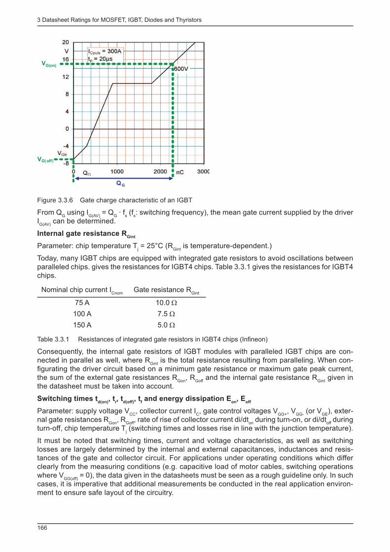
3 Datasheet Ratings for MOSFET, IGBT, Diodes and Thyristors
166
VG( off)
VG(on)
Q G
Figure 3.3.6 Gate charge characteristic of an IGBT
From Q G using I
G(AV) = Q
G · f
s (f
s : switching frequency), the mean gate current supplied by the driver
I G(AV)
can be determined.
Internal gate resistance R Gint
Parameter: chip temperature T j = 25°C (R
Gint is temperature-dependent.)
Today, many IGBT chips are equipped with integrated gate resistors to avoid oscillations between paralleled chips. gives the resistances for IGBT4 chips. Table 3.3.1 gives the resistances for IGBT4 chips.
Nominal chip current I Cnom
Gate resistance R Gint
75 A 10.0 Ω
100 A 7.5 Ω
150 A 5.0 Ω
Table 3.3.1 Resistances of integrated gate resistors in IGBT4 chips (Infi neon)
Consequently, the internal gate resistors of IGBT modules with paralleled IGBT chips are con-nected in parallel as well, where R
Gint is the total resistance resulting from paralleling. When con-
fi gurating the driver circuit based on a minimum gate resistance or maximum gate peak current, the sum of the external gate resistances R
Gon , R
Goff and the internal gate resistance R
Gint given in
the datasheet must be taken into account.
Switching times t d(on)
, t r , t
d(off) , t
f and energy dissipation E
on , E
off
Parameter: supply voltage V CC
, collector current I C , gate control voltages V
GG+ , V
GG- (or V
GE ), exter-
nal gate resistances R Gon
, R Goff
, rate of rise of collector current di/dt on
during turn-on, or di/dt off
during turn-off, chip temperature T
j (switching times and losses rise in line with the junction temperature).
It must be noted that switching times, current and voltage characteristics, as well as switching losses are largely determined by the internal and external capacitances, inductances and resis-tances of the gate and collector circuit. For applications under operating conditions which differ clearly from the measuring conditions (e.g. capacitive load of motor cables, switching operations where V
GG(off) = 0), the data given in the datasheets must be seen as a rough guideline only. In such
cases, it is imperative that additional measurements be conducted in the real application environ-ment to ensure safe layout of the circuitry.

3 Datasheet Ratings for MOSFET, IGBT, Diodes and Thyristors
167
Switching times indicated in IGBT datasheets are determined from a measuring circuit under ohm-ic-inductive load in accordance with Figure 3.2.14a. The load time constant L/R is high compared to the switching frequency cycle duration T = 1/f, meaning that the load inductance generates a continuous current. When the IGBT is in blocking state, this will fl ow through the freewheeling di-ode, commutate to the IGBT during turn-on and back to the freewheeling diode on turn-off (hard switching). Switching times refer to the gate-emitter voltage and collector current characteristics during turn-on and turn-off; cf. explanations on the physical background of current and voltage characteristics in chapter 2.4.2.2.
+15 V
VGG+
VGG-
-15 V
0 V
RGon
RGoff
vGE
E
Ex
vCE
L
IL
VCC
R
iC
vGE
VGG+
vGE
10%
90%
t
t
iC
IL
10% IL
90% IL
10% IL
90% IL
td(on) tr
ton toff
td(off) tf
vCE
VCC
Turn-on Turn-offt
VGG-
idealized waveform
a)
b)
Figure 3.3.7 Switching times of IGBT: a) Measuring circuit; b) Defi nition of switching times under ohmic-inductive load
The turn-on delay time t d(on)
is defi ned as the time interval between the moment when the gate-emitter voltage v
GE has reached 10% of its end value and the collector current i
C has increased
to 10% of the load current. During the subsequent rise time t r , the collector current i
C increases
from 10% to 90% of the load current. The sum of turn-on delay time t d(on)
and rise time t r is called
turn-on time t on
.
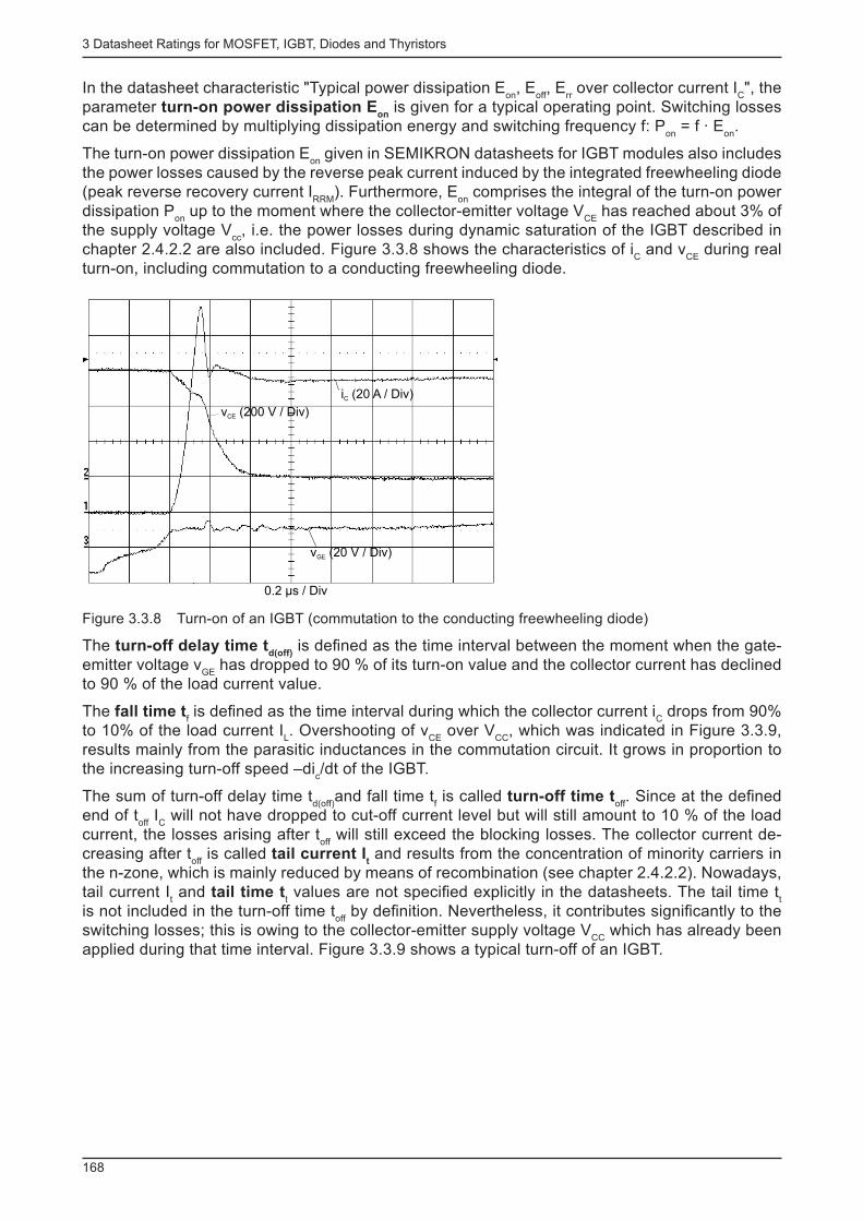
3 Datasheet Ratings for MOSFET, IGBT, Diodes and Thyristors
168
In the datasheet characteristic "Typical power dissipation E on
, E off
, E rr over collector current I
C ", the
parameter turn-on power dissipation E on
is given for a typical operating point. Switching losses can be determined by multiplying dissipation energy and switching frequency f: P
on = f · E
on .
The turn-on power dissipation E on
given in SEMIKRON datasheets for IGBT modules also includes the power losses caused by the reverse peak current induced by the integrated freewheeling diode (peak reverse recovery current I
RRM ). Furthermore, E
on comprises the integral of the turn-on power
dissipation P on
up to the moment where the collector-emitter voltage V CE
has reached about 3% of the supply voltage V
cc , i.e. the power losses during dynamic saturation of the IGBT described in
chapter 2.4.2.2 are also included. Figure 3.3.8 shows the characteristics of i C and v
CE during real
turn-on, including commutation to a conducting freewheeling diode.
v (200 V / Div)CE
i (20 A / Div)C
v (20 V / Div)GE
0.2 µs / Div
Figure 3.3.8 Turn-on of an IGBT (commutation to the conducting freewheeling diode)
The turn-off delay time t d(off)
is defi ned as the time interval between the moment when the gate-emitter voltage v
GE has dropped to 90 % of its turn-on value and the collector current has declined
to 90 % of the load current value.
The fall time t f is defi ned as the time interval during which the collector current i
C drops from 90%
to 10% of the load current I L . Overshooting of v
CE over V
CC , which was indicated in Figure 3.3.9,
results mainly from the parasitic inductances in the commutation circuit. It grows in proportion to the increasing turn-off speed –di
c /dt of the IGBT.
The sum of turn-off delay time t d(off)
and fall time t f is called turn-off time t
off . Since at the defi ned
end of t off
I C will not have dropped to cut-off current level but will still amount to 10 % of the load
current, the losses arising after t off
will still exceed the blocking losses. The collector current de-creasing after t
off is called tail current I
t and results from the concentration of minority carriers in
the n-zone, which is mainly reduced by means of recombination (see chapter 2.4.2.2). Nowadays, tail current I
t and tail time t
t values are not specifi ed explicitly in the datasheets. The tail time t
t
is not included in the turn-off time t off
by defi nition. Nevertheless, it contributes signifi cantly to the switching losses; this is owing to the collector-emitter supply voltage V
CC which has already been
applied during that time interval. Figure 3.3.9 shows a typical turn-off of an IGBT.
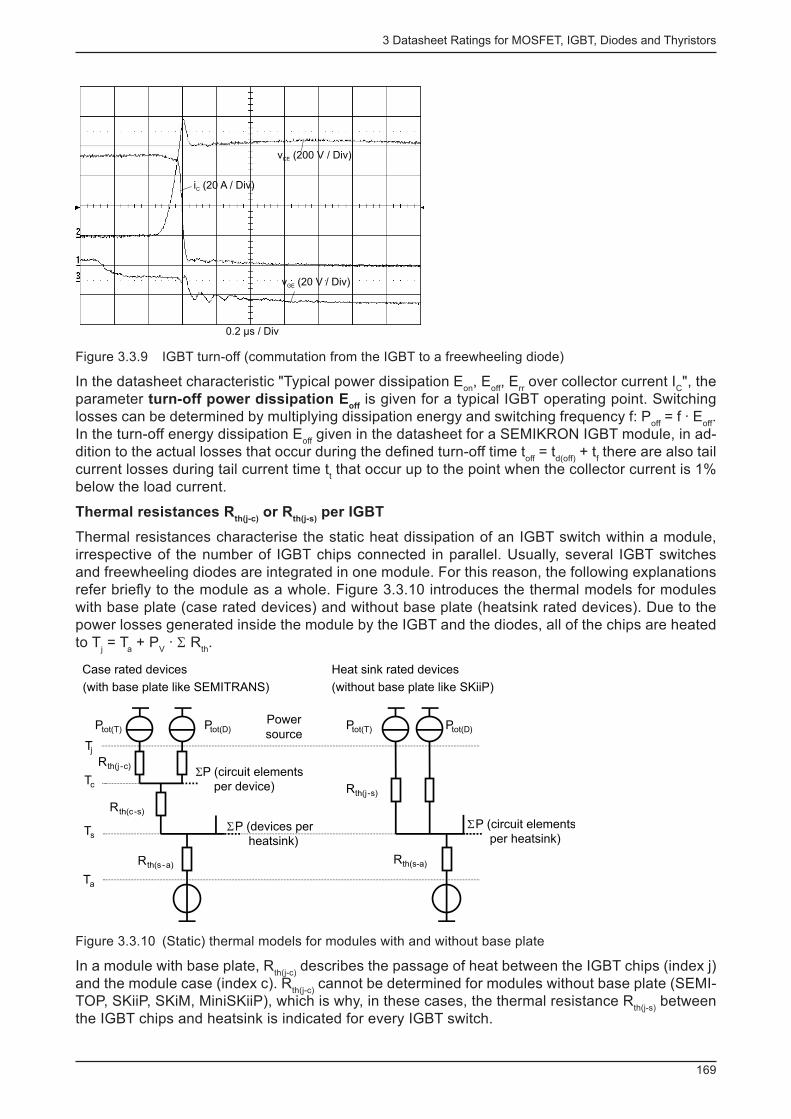
3 Datasheet Ratings for MOSFET, IGBT, Diodes and Thyristors
169
i (20 A / Div)C
v (200 V / Div)CE
v (20 V / Div)GE
0.2 µs / Div
Figure 3.3.9 IGBT turn-off (commutation from the IGBT to a freewheeling diode)
In the datasheet characteristic "Typical power dissipation E on
, E off
, E rr over collector current I
C ", the
parameter turn-off power dissipation E off
is given for a typical IGBT operating point. Switching losses can be determined by multiplying dissipation energy and switching frequency f: P
off = f · E
off .
In the turn-off energy dissipation E off
given in the datasheet for a SEMIKRON IGBT module, in ad-dition to the actual losses that occur during the defi ned turn-off time t
off = t
d(off) + t
f there are also tail
current losses during tail current time t t that occur up to the point when the collector current is 1%
below the load current.
Thermal resistances R th(j-c)
or R th(j-s)
per IGBT
Thermal resistances characterise the static heat dissipation of an IGBT switch within a module, irrespective of the number of IGBT chips connected in parallel. Usually, several IGBT switches and freewheeling diodes are integrated in one module. For this reason, the following explanations refer briefl y to the module as a whole. Figure 3.3.10 introduces the thermal models for modules with base plate (case rated devices) and without base plate (heatsink rated devices). Due to the power losses generated inside the module by the IGBT and the diodes, all of the chips are heated to T
j = T
a + P
V · Σ R
th .
Heat sink rated devices
(without base plate like SKiiP)
SP (circuit elements
per device)
SP (devices per
heatsink)Ts
Tc
Tj
Rth(s -a)
Rth(c-s)
Rth(j -c)
Ta
Rth(s-a)
Rth(j -s)
SP (circuit elements
per heatsink)
Power
sourcePtot(T) Ptot(D) Ptot(T) Ptot(D)
Case rated devices
(with base plate like SEMITRANS)
Figure 3.3.10 (Static) thermal models for modules with and without base plate
In a module with base plate, R th(j-c)
describes the passage of heat between the IGBT chips (index j) and the module case (index c). R
th(j-c) cannot be determined for modules without base plate (SEMI-
TOP, SKiiP, SKiM, MiniSKiiP), which is why, in these cases, the thermal resistance R th(j-s)
between the IGBT chips and heatsink is indicated for every IGBT switch.
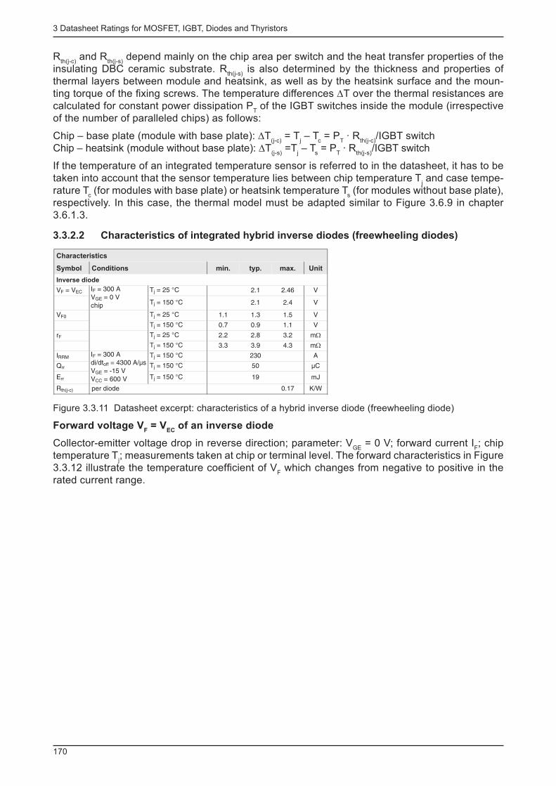
3 Datasheet Ratings for MOSFET, IGBT, Diodes and Thyristors
170
R th(j-c)
and R th(j-s)
depend mainly on the chip area per switch and the heat transfer properties of the insulating DBC ceramic substrate. R
th(j-s) is also determined by the thickness and properties of
thermal layers between module and heatsink, as well as by the heatsink surface and the moun-ting torque of the fi xing screws. The temperature differences ∆T over the thermal resistances are calculated for constant power dissipation P
T of the IGBT switches inside the module (irrespective
of the number of paralleled chips) as follows:
Chip – base plate (module with base plate): ∆T (j-c)
= T j – T
c = P
T · R
th(j-c) /IGBT switch
Chip – heatsink (module without base plate): ∆T (j-s)
=T j – T
s = P
T · R
th(j-s) /IGBT switch
If the temperature of an integrated temperature sensor is referred to in the datasheet, it has to be taken into account that the sensor temperature lies between chip temperature T
j and case tempe-
rature T c (for modules with base plate) or heatsink temperature T
s (for modules without base plate),
respectively. In this case, the thermal model must be adapted similar to Figure 3.6.9 in chapter 3.6.1.3.
3.3.2.2 Characteristics of integrated hybrid inverse diodes (freewheeling diodes)
Characteristics
Symbol Conditions min. typ. max. Unit
Inverse diode
VF = VEC IF = 300 A
VGE = 0 V
chip
Tj = 25 °C 2.1 2.46 V
Tj = 150 °C 2.1 2.4 V
VF0 Tj = 25 °C 1.1 1.3 1.5 V
Tj = 150 °C 0.7 0.9 1.1 V
rF Tj = 25 °C 2.2 2.8 3.2 m
Tj = 150 °C 3.3 3.9 4.3 m
IRRMIF = 300 A
di/dtoff = 4300 A/µs
VGE = -15 V
VCC = 600 V
Tj = 150 °C 230 A
Qrr Tj = 150 °C 50 µC
Err Tj = 150 °C 19 mJ
Rth(j-c) per diode 0.17 K/W
Figure 3.3.11 Datasheet excerpt: characteristics of a hybrid inverse diode (freewheeling diode)
Forward voltage V F = V
EC of an inverse diode
Collector-emitter voltage drop in reverse direction; parameter: V GE
= 0 V; forward current I F ; chip
temperature T j ; measurements taken at chip or terminal level. The forward characteristics in Figure
3.3.12 illustrate the temperature coeffi cient of V F which changes from negative to positive in the
rated current range.
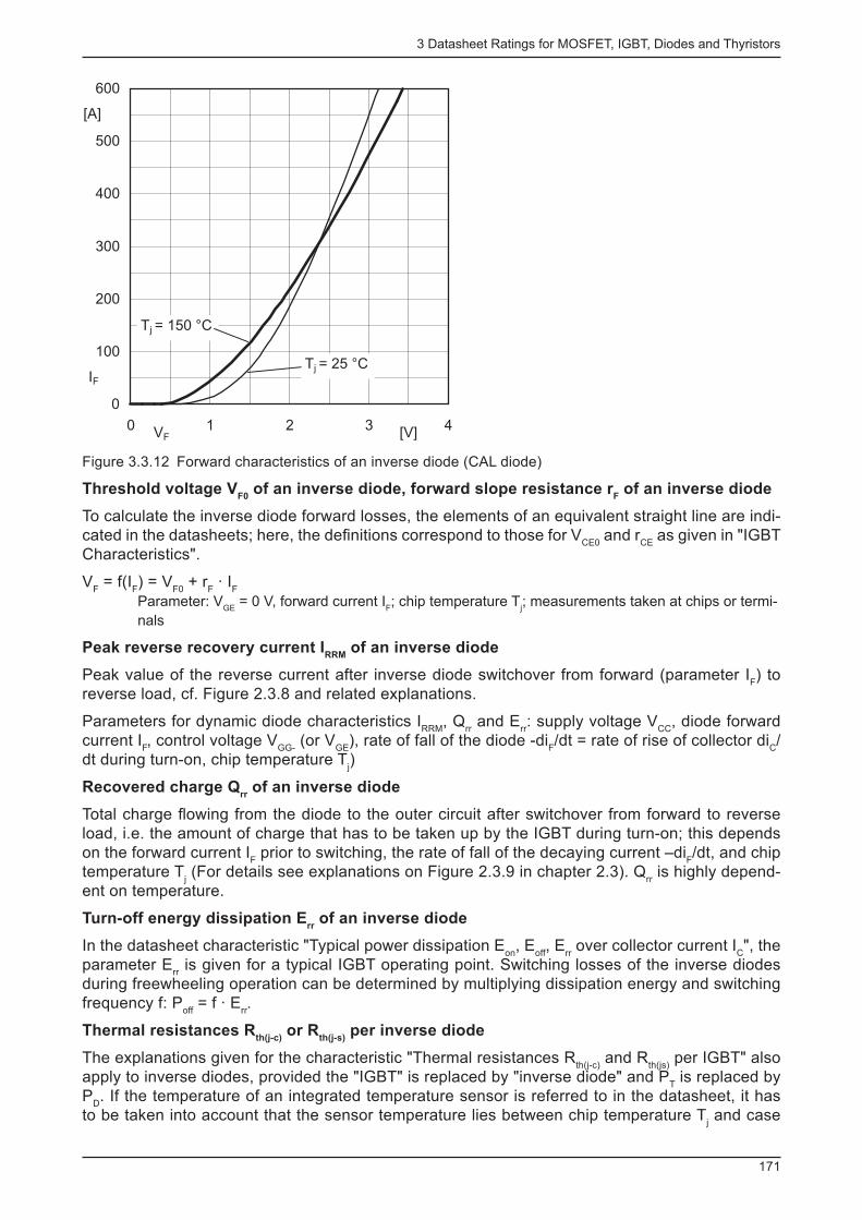
3 Datasheet Ratings for MOSFET, IGBT, Diodes and Thyristors
171
0
100
200
300
400
500
600
0 1 2 3 4VF
T = 150 °Cj
[A]
[V]
IFT = 25 °Cj
Figure 3.3.12 Forward characteristics of an inverse diode (CAL diode)
Threshold voltage V F0
of an inverse diode, forward slope resistance r F of an inverse diode
To calculate the inverse diode forward losses, the elements of an equivalent straight line are indi-cated in the datasheets; here, the defi nitions correspond to those for V
CE0 and r
CE as given in "IGBT
Characteristics".
V F = f(I
F ) = V
F0 + r
F · I
F
Parameter: V GE
= 0 V, forward current I F ; chip temperature T
j ; measurements taken at chips or termi-
nals
Peak reverse recovery current I RRM
of an inverse diode
Peak value of the reverse current after inverse diode switchover from forward (parameter I F ) to
reverse load, cf. Figure 2.3.8 and related explanations.
Parameters for dynamic diode characteristics I RRM
, Q rr and E
rr : supply voltage V
CC , diode forward
current I F , control voltage V
GG- (or V
GE ), rate of fall of the diode -di
F /dt = rate of rise of collector di
C /
dt during turn-on, chip temperature T j )
Recovered charge Q rr of an inverse diode
Total charge fl owing from the diode to the outer circuit after switchover from forward to reverse load, i.e. the amount of charge that has to be taken up by the IGBT during turn-on; this depends on the forward current I
F prior to switching, the rate of fall of the decaying current –di
F /dt, and chip
temperature T j (For details see explanations on Figure 2.3.9 in chapter 2.3). Q
rr is highly depend-
ent on temperature.
Turn-off energy dissipation E rr of an inverse diode
In the datasheet characteristic "Typical power dissipation E on
, E off
, E rr over collector current I
C ", the
parameter E rr is given for a typical IGBT operating point. Switching losses of the inverse diodes
during freewheeling operation can be determined by multiplying dissipation energy and switching frequency f: P
off = f · E
rr .
Thermal resistances R th(j-c)
or R th(j-s)
per inverse diode
The explanations given for the characteristic "Thermal resistances R th(j-c)
and R th(js)
per IGBT" also apply to inverse diodes, provided the "IGBT" is replaced by "inverse diode" and P
T is replaced by
P D . If the temperature of an integrated temperature sensor is referred to in the datasheet, it has
to be taken into account that the sensor temperature lies between chip temperature T j and case
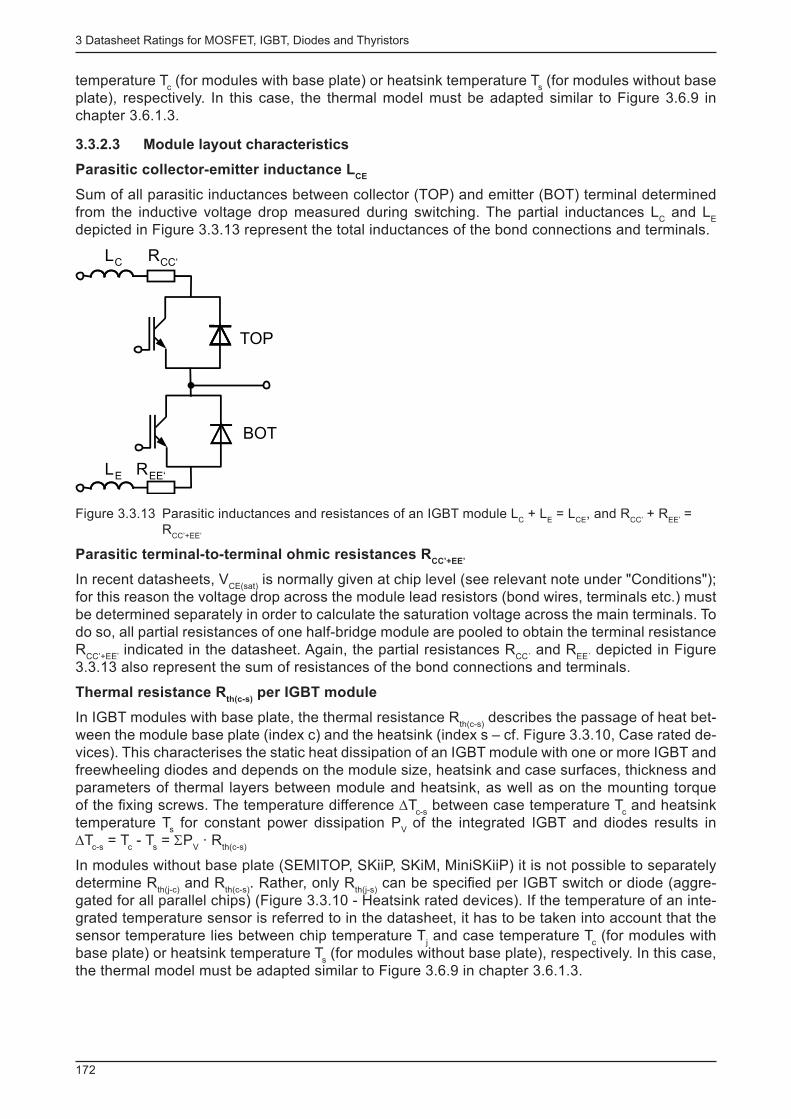
3 Datasheet Ratings for MOSFET, IGBT, Diodes and Thyristors
172
temperature T c (for modules with base plate) or heatsink temperature T
s (for modules without base
plate), respectively. In this case, the thermal model must be adapted similar to Figure 3.6.9 in chapter 3.6.1.3.
3.3.2.3 Module layout characteristics
Parasitic collector-emitter inductance L CE
Sum of all parasitic inductances between collector (TOP) and emitter (BOT) terminal determined from the inductive voltage drop measured during switching. The partial inductances L
C and L
E
depicted in Figure 3.3.13 represent the total inductances of the bond connections and terminals.
LC
LE REE‘
RCC‘
TOP
BOT
Figure 3.3.13 Parasitic inductances and resistances of an IGBT module L C + L
E = L
CE , and R
CC’ + R
EE’ =
R CC’+EE’
Parasitic terminal-to-terminal ohmic resistances R CC’+EE’
In recent datasheets, V CE(sat)
is normally given at chip level (see relevant note under "Conditions"); for this reason the voltage drop across the module lead resistors (bond wires, terminals etc.) must be determined separately in order to calculate the saturation voltage across the main terminals. To do so, all partial resistances of one half-bridge module are pooled to obtain the terminal resistance R
CC’+EE’ indicated in the datasheet. Again, the partial resistances R
CC´ and R
EE´ depicted in Figure
3.3.13 also represent the sum of resistances of the bond connections and terminals.
Thermal resistance R th(c-s)
per IGBT module
In IGBT modules with base plate, the thermal resistance R th(c-s)
describes the passage of heat bet-ween the module base plate (index c) and the heatsink (index s – cf. Figure 3.3.10, Case rated de-vices). This characterises the static heat dissipation of an IGBT module with one or more IGBT and freewheeling diodes and depends on the module size, heatsink and case surfaces, thickness and parameters of thermal layers between module and heatsink, as well as on the mounting torque of the fi xing screws. The temperature difference ∆T
c-s between case temperature T
c and heatsink
temperature T s for constant power dissipation P
V of the integrated IGBT and diodes results in
∆T c-s
= T c - T
s = ΣP
V · R
th(c-s)
In modules without base plate (SEMITOP, SKiiP, SKiM, MiniSKiiP) it is not possible to separately determine R
th(j-c) and R
th(c-s) . Rather, only R
th(j-s) can be specifi ed per IGBT switch or diode (aggre-
gated for all parallel chips) (Figure 3.3.10 - Heatsink rated devices). If the temperature of an inte-grated temperature sensor is referred to in the datasheet, it has to be taken into account that the sensor temperature lies between chip temperature T
j and case temperature T
c (for modules with
base plate) or heatsink temperature T s (for modules without base plate), respectively. In this case,
the thermal model must be adapted similar to Figure 3.6.9 in chapter 3.6.1.3.
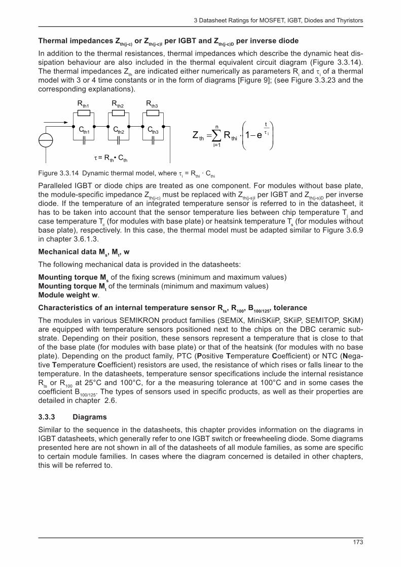
3 Datasheet Ratings for MOSFET, IGBT, Diodes and Thyristors
173
Thermal impedances Z th(j-c)
or Z th(j-c)I
per IGBT and Z th(j-c)D
per inverse diode
In addition to the thermal resistances, thermal impedances which describe the dynamic heat dis-sipation behaviour are also included in the thermal equivalent circuit diagram (Figure 3.3.14). The thermal impedances Z
th are indicated either numerically as parameters R
i and τ
i of a thermal
model with 3 or 4 time constants or in the form of diagrams [Figure 9]; (see Figure 3.3.23 and the corresponding explanations).
÷÷ø
öççè
æ-×= tå i
tn
thith eRZ 1i=1
Rth1 Rth2 Rth3
Cth1 Cth2 Cth3
t = R th• Cth
Figure 3.3.14 Dynamic thermal model, where τ i = R
thi · C
thi
Paralleled IGBT or diode chips are treated as one component. For modules without base plate, the module-specifi c impedance Z
th(j-c) must be replaced with Z
th(j-s)I per IGBT and Z
th(j-s)D per inverse
diode. If the temperature of an integrated temperature sensor is referred to in the datasheet, it has to be taken into account that the sensor temperature lies between chip temperature T
j and
case temperature T c (for modules with base plate) or heatsink temperature T
s (for modules without
base plate), respectively. In this case, the thermal model must be adapted similar to Figure 3.6.9 in chapter 3.6.1.3.
Mechanical data M s , M
t , w
The following mechanical data is provided in the datasheets:
Mounting torque M s of the fi xing screws (minimum and maximum values)
Mounting torque M t of the terminals (minimum and maximum values)
Module weight w .
Characteristics of an internal temperature sensor R ts , R
100 , B
100/125 , tolerance
The modules in various SEMIKRON product families (SEMiX, MiniSKiiP, SKiiP, SEMITOP, SKiM) are equipped with temperature sensors positioned next to the chips on the DBC ceramic sub-strate. Depending on their position, these sensors represent a temperature that is close to that of the base plate (for modules with base plate) or that of the heatsink (for modules with no base plate). Depending on the product family, PTC ( P ositive T emperature C oeffi cient) or NTC ( N ega-tive T emperature C oeffi cient) resistors are used, the resistance of which rises or falls linear to the temperature. In the datasheets, temperature sensor specifi cations include the internal resistance R
ts or R
100 at 25°C and 100°C, for a the measuring tolerance at 100°C and in some cases the
coeffi cient B 100/125
. The types of sensors used in specifi c products, as well as their properties are detailed in chapter 2.6.
3.3.3 Diagrams
Similar to the sequence in the datasheets, this chapter provides information on the diagrams in IGBT datasheets, which generally refer to one IGBT switch or freewheeling diode. Some diagrams presented here are not shown in all of the datasheets of all module families, as some are specifi c to certain module families. In cases where the diagram concerned is detailed in other chapters, this will be referred to.
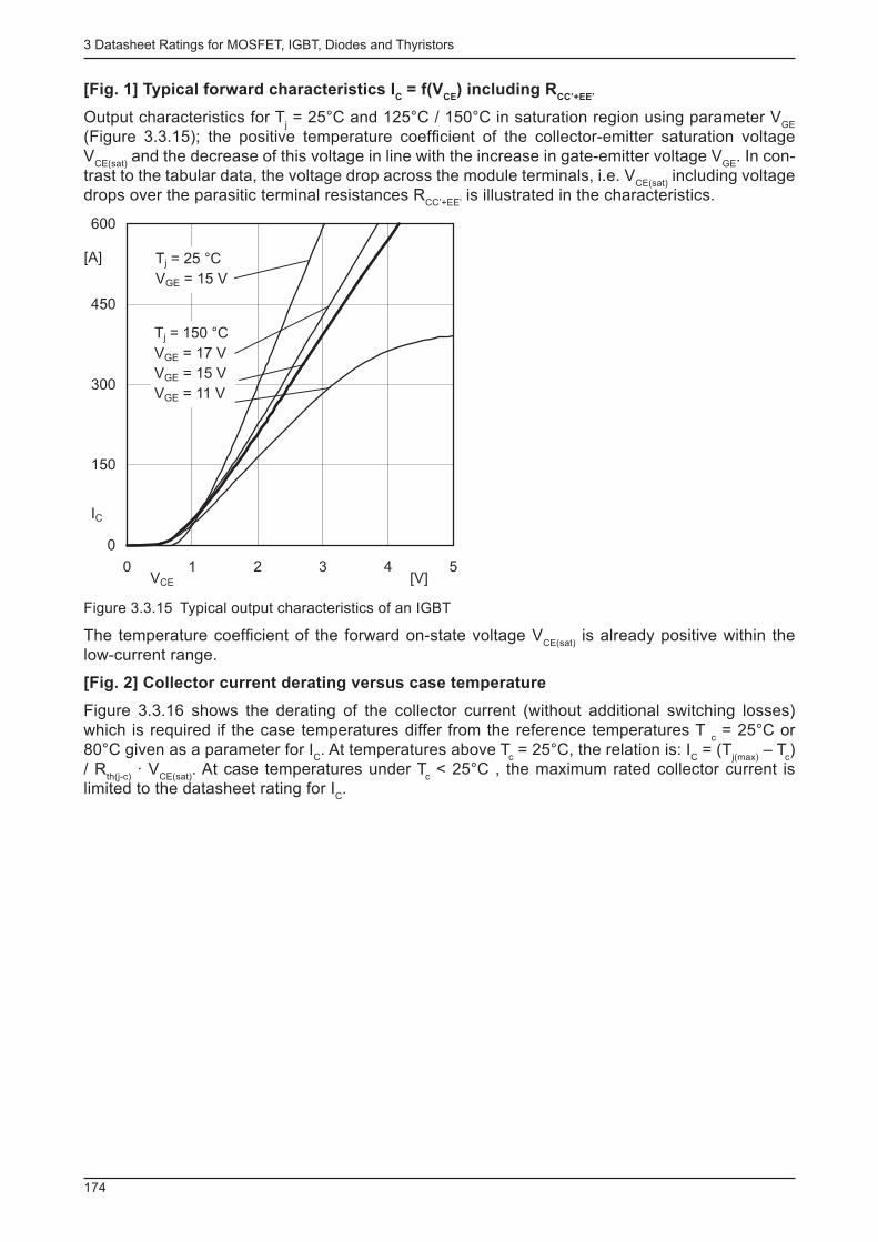
3 Datasheet Ratings for MOSFET, IGBT, Diodes and Thyristors
174
[Fig. 1] Typical forward characteristics I C = f(V
CE ) including R
CC’+EE’
Output characteristics for T j = 25°C and 125°C / 150°C in saturation region using parameter V
GE
(Figure 3.3.15); the positive temperature coeffi cient of the collector-emitter saturation voltage V
CE(sat) and the decrease of this voltage in line with the increase in gate-emitter voltage V
GE . In con-
trast to the tabular data, the voltage drop across the module terminals, i.e. V CE(sat)
including voltage drops over the parasitic terminal resistances R
CC’+EE’ is illustrated in the characteristics.
0
150
300
450
600
0 1 2 3 4 5[V]
IC
T = 25 °Cj
V = 15 VGE
T = 150 °Cj
V = 17 VGE
V = 15 VGE
V = 11 VGE
[A]
VCE
Figure 3.3.15 Typical output characteristics of an IGBT
The temperature coeffi cient of the forward on-state voltage V CE(sat)
is already positive within the low-current range.
[Fig. 2] Collector current derating versus case temperature
Figure 3.3.16 shows the derating of the collector current (without additional switching losses) which is required if the case temperatures differ from the reference temperatures T
c = 25°C or
80°C given as a parameter for I C . At temperatures above T
c = 25°C, the relation is: I
C = (T
j(max) – T
c )
/ R th(j-c)
· V CE(sat)
. At case temperatures under T c < 25°C , the maximum rated collector current is
limited to the datasheet rating for I C .
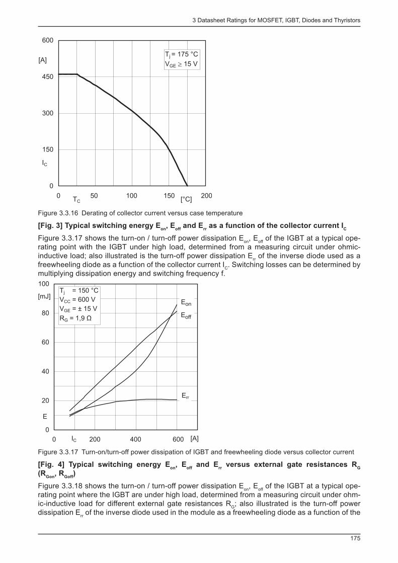
3 Datasheet Ratings for MOSFET, IGBT, Diodes and Thyristors
175
0
150
300
450
600
0 50 100 150 200[°C]
[A]Tj = 175 °C
V 15 VGE ≥
T
I
C
C
Figure 3.3.16 Derating of collector current versus case temperature
[Fig. 3] Typical switching energy E on
, E off
and E rr as a function of the collector current I
C
Figure 3.3.17 shows the turn-on / turn-off power dissipation E on
, E off
of the IGBT at a typical ope-rating point with the IGBT under high load, determined from a measuring circuit under ohmic-inductive load; also illustrated is the turn-off power dissipation E
rr of the inverse diode used as a
freewheeling diode as a function of the collector current I C . Switching losses can be determined by
multiplying dissipation energy and switching frequency f.
0
20
40
60
80
100
0 200 400 600 [A]
[mJ]Eon
Eoff
Err
T = 150 °Cj
V = 600 VCC
V = ± 15 VGE
R = 1,9G Ω
I
E
C
Figure 3.3.17 Turn-on/turn-off power dissipation of IGBT and freewheeling diode versus collector current
[Fig. 4] Typical switching energy E on
, E off
and E rr versus external gate resistances R
G
(R Gon
, R Goff
)
Figure 3.3.18 shows the turn-on / turn-off power dissipation E on
, E off
of the IGBT at a typical ope-rating point where the IGBT are under high load, determined from a measuring circuit under ohm-ic-inductive load for different external gate resistances R
G ; also illustrated is the turn-off power
dissipation E rr of the inverse diode used in the module as a freewheeling diode as a function of the
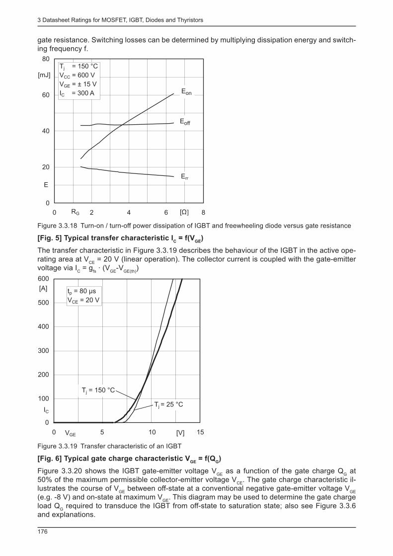
3 Datasheet Ratings for MOSFET, IGBT, Diodes and Thyristors
176
gate resistance. Switching losses can be determined by multiplying dissipation energy and switch-ing frequency f.
0
20
40
60
80
0 2 4 6 8[Ω]
[mJ]
Eon
Eoff
Err
T = 150 °Cj
V = 600 VCC
V = ± 15 VGE
I = 300 AC
E
RG
Figure 3.3.18 Turn-on / turn-off power dissipation of IGBT and freewheeling diode versus gate resistance
[Fig. 5] Typical transfer characteristic I C = f(V
GE )
The transfer characteristic in Figure 3.3.19 describes the behaviour of the IGBT in the active ope-rating area at V
CE = 20 V (linear operation). The collector current is coupled with the gate-emitter
voltage via I C = g
fs · (V
GE -V
GE(th) )
0
100
200
300
400
500
600
0 5 10 15[V]
[A]
T = 150 °Cj
T = 25 °Cj
t = 80 µsp
V = 20 VCE
I
V
C
GE
Figure 3.3.19 Transfer characteristic of an IGBT
[Fig. 6] Typical gate charge characteristic V GE
= f(Q G )
Figure 3.3.20 shows the IGBT gate-emitter voltage V GE
as a function of the gate charge Q G at
50% of the maximum permissible collector-emitter voltage V CE
. The gate charge characteristic il-lustrates the course of V
GE between off-state at a conventional negative gate-emitter voltage V
GE
(e.g. -8 V) and on-state at maximum V GE
. This diagram may be used to determine the gate charge load Q
G required to transduce the IGBT from off-state to saturation state; also see Figure 3.3.6
and explanations.
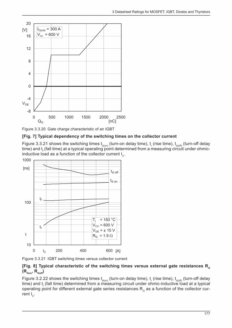
3 Datasheet Ratings for MOSFET, IGBT, Diodes and Thyristors
177
-8
-4
0
4
8
12
16
20
0 500 1000 1500 2000 2500[nC]
[V] I = 300 ACpuls
V = 600 Vcc
V
Q
GE
G
Figure 3.3.20 Gate charge characteristic of an IGBT
[Fig. 7] Typical dependency of the switching times on the collector current
Figure 3.3.21 shows the switching times t d(on)
(turn-on delay time), t r (rise time), t
d(off) (turn-off delay
time) and t f (fall time) at a typical operating point determined from a measuring circuit under ohmic-
inductive load as a function of the collector current I C .
10
100
1000
0 200 400 600 [A]
[ns]td off
td on
tr
tf
T = 150 °Cj
V = 600 VCC
V = ± 15 VGE
R = 1.9G Wt
IC
Figure 3.3.21 IGBT switching times versus collector current
[Fig. 8] Typical characteristic of the switching times versus external gate resistances R G
(R Gon
, R Goff
)
Figure 3.2.22 shows the switching times t d(on)
(turn-on delay time), t r (rise time), t
d(off) (turn-off delay
time) and t f (fall time) determined from a measuring circuit under ohmic-inductive load at a typical
operating point for different external gate series resistances R G as a function of the collector cur-
rent I C .
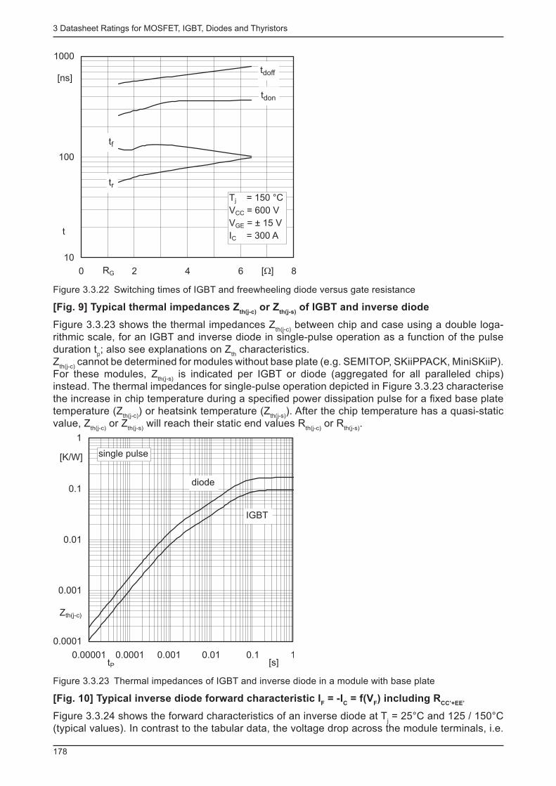
3 Datasheet Ratings for MOSFET, IGBT, Diodes and Thyristors
178
10
100
1000
0 2 4 6 8
tr
t
[ns]tdoff
tdon
tf
T = 150 °Cj
V = 600 VCC
V = ± 15 VGE
I = 300 AC
RG [ ]W
Figure 3.3.22 Switching times of IGBT and freewheeling diode versus gate resistance
[Fig. 9] Typical thermal impedances Z th(j-c)
or Z th(j-s)
of IGBT and inverse diode
Figure 3.3.23 shows the thermal impedances Z th(j-c)
between chip and case using a double loga-rithmic scale, for an IGBT and inverse diode in single-pulse operation as a function of the pulse duration t
p ; also see explanations on Z
th characteristics.
Z th(j-c)
cannot be determined for modules without base plate (e.g. SEMITOP, SKiiPPACK, MiniSKiiP). For these modules, Z
th(j-s) is indicated per IGBT or diode (aggregated for all paralleled chips)
instead. The thermal impedances for single-pulse operation depicted in Figure 3.3.23 characterise the increase in chip temperature during a specifi ed power dissipation pulse for a fi xed base plate temperature (Z
th(j-c) ) or heatsink temperature (Z
th(j-s) ). After the chip temperature has a quasi-static
value, Z th(j-c)
or Z th(j-s)
will reach their static end values R th(j-c)
or R th(j-s)
.
0.0001
0.001
0.01
0.1
1
0.00001 0.0001 0.001 0.01 0.1 1
single pulse[K/W]
[s]
Z
t
th(j-c)
P
diode
IGBT
Figure 3.3.23 Thermal impedances of IGBT and inverse diode in a module with base plate
[Fig. 10] Typical inverse diode forward characteristic I F = -I
C = f(V
F ) including R
CC’+EE’
Figure 3.3.24 shows the forward characteristics of an inverse diode at T j = 25°C and 125 / 150°C
(typical values). In contrast to the tabular data, the voltage drop across the module terminals, i.e.
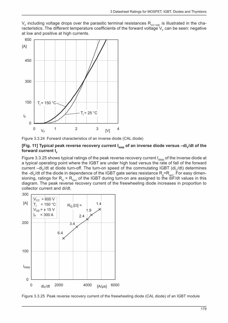
3 Datasheet Ratings for MOSFET, IGBT, Diodes and Thyristors
179
V F including voltage drops over the parasitic terminal resistances R
CC’+EE’ is illustrated in the cha-
racteristics. The different temperature coeffi cients of the forward voltage V F can be seen: negative
at low and positive at high currents.
0
150
300
450
600
0 1 2 3 4VF
T = 150 °Cj
[A]
[V]
IFT = 25 °Cj
Figure 3.3.24 Forward characteristics of an inverse diode (CAL diode)
[Fig. 11] Typical peak reverse recovery current I RRM
of an inverse diode versus –di F /dt of the
forward current I F
Figure 3.3.25 shows typical ratings of the peak reverse recovery current I RRM
of the inverse diode at a typical operating point where the IGBT are under high load versus the rate of fall of the forward current –di
F /dt at diode turn-off. The turn-on speed of the commutating IGBT (di
C /dt) determines
the -di F /dt of the diode in dependence of the IGBT gate series resistance R
g =R
gon . For easy dimen-
sioning, ratings for R G = R
Gon of the IGBT during turn-on are assigned to the diF/dt values in this
diagram. The peak reverse recovery current of the freewheeling diode increases in proportion to collector current and di/dt.
0
100
200
300
0 2000 4000 6000
[A]
3.4
2.4
6.4
1.9
R [ ] =G W 1.4
V = 600 VCC
T = 150 °Cj
V = ± 15 VGE
I = 300 AF
di /dtF [A/µs]
IRRM
Figure 3.3.25 Peak reverse recovery current of the freewheeling diode (CAL diode) of an IGBT module
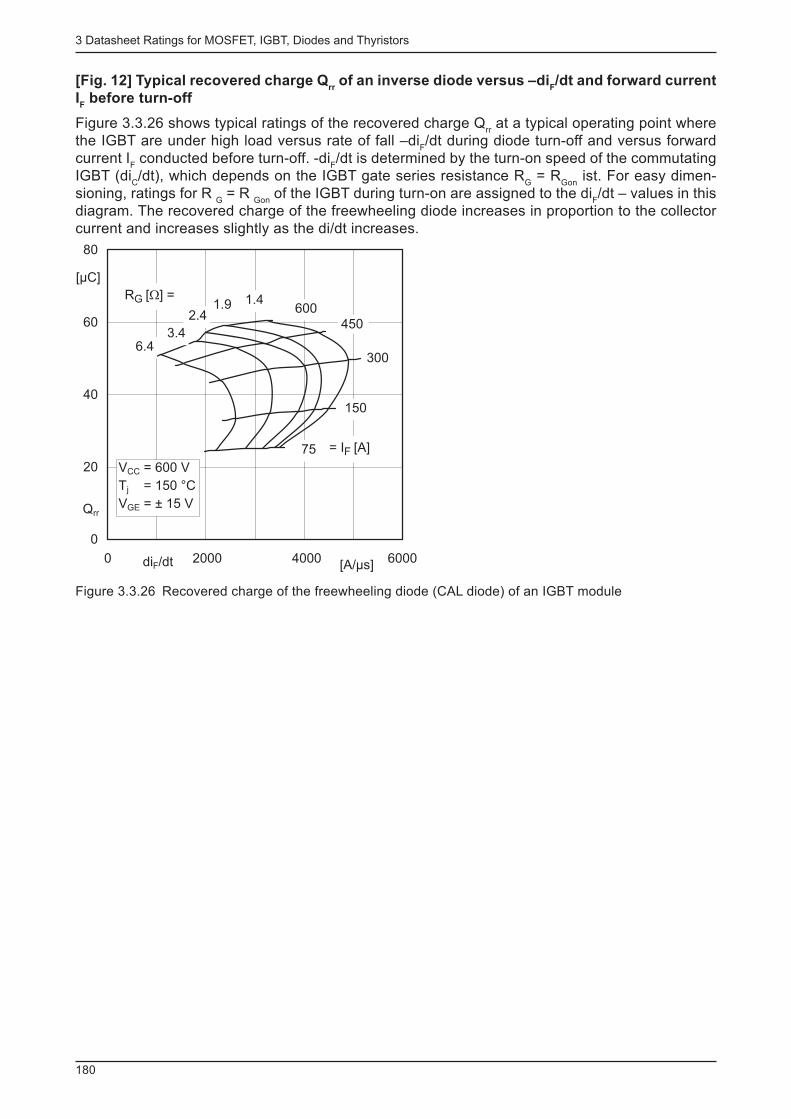
3 Datasheet Ratings for MOSFET, IGBT, Diodes and Thyristors
180
[Fig. 12] Typical recovered charge Q rr of an inverse diode versus –di
F /dt and forward current
I F before turn-off
Figure 3.3.26 shows typical ratings of the recovered charge Q rr at a typical operating point where
the IGBT are under high load versus rate of fall –di F /dt during diode turn-off and versus forward
current I F conducted before turn-off. -di
F /dt is determined by the turn-on speed of the commutating
IGBT (di C /dt), which depends on the IGBT gate series resistance R
G = R
Gon ist. For easy dimen-
sioning, ratings for R G = R
Gon of the IGBT during turn-on are assigned to the di
F /dt – values in this
diagram. The recovered charge of the freewheeling diode increases in proportion to the collector current and increases slightly as the di/dt increases.
0
20
40
60
80
0 2000 4000 6000[A/µs]
[µC]
= I [A]F
450
150
75
3.4
2.4
6.4
1.9R [ ] =G W 1.4
600
V = 600 VCC
T = 150 °Cj
V = ± 15 VGE
300
di /dtF
Qrr
Figure 3.3.26 Recovered charge of the freewheeling diode (CAL diode) of an IGBT module
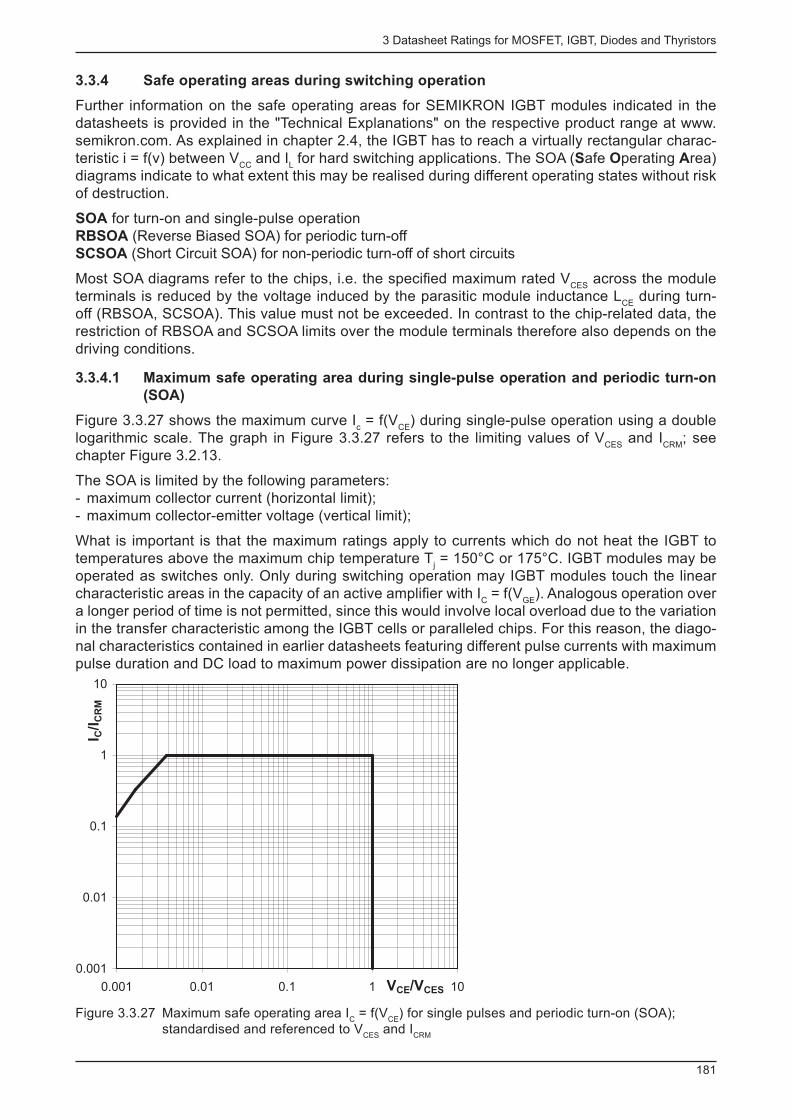
3 Datasheet Ratings for MOSFET, IGBT, Diodes and Thyristors
181
3.3.4 Safe operating areas during switching operation
Further information on the safe operating areas for SEMIKRON IGBT modules indicated in the datasheets is provided in the "Technical Explanations" on the respective product range at www.semikron.com. As explained in chapter 2.4, the IGBT has to reach a virtually rectangular charac-teristic i = f(v) between V
CC and I
L for hard switching applications. The SOA ( S afe O perating A rea)
diagrams indicate to what extent this may be realised during different operating states without risk of destruction.
SOA for turn-on and single-pulse operation RBSOA (Reverse Biased SOA) for periodic turn-off SCSOA (Short Circuit SOA) for non-periodic turn-off of short circuits
Most SOA diagrams refer to the chips, i.e. the specifi ed maximum rated V CES
across the module terminals is reduced by the voltage induced by the parasitic module inductance L
CE during turn-
off (RBSOA, SCSOA). This value must not be exceeded. In contrast to the chip-related data, the restriction of RBSOA and SCSOA limits over the module terminals therefore also depends on the driving conditions.
3.3.4.1 Maximum safe operating area during single-pulse operation and periodic turn-on
(SOA)
Figure 3.3.27 shows the maximum curve I c = f(V
CE ) during single-pulse operation using a double
logarithmic scale. The graph in Figure 3.3.27 refers to the limiting values of V CES
and I CRM
; see chapter Figure 3.2.13.
The SOA is limited by the following parameters: - maximum collector current (horizontal limit); - maximum collector-emitter voltage (vertical limit);
What is important is that the maximum ratings apply to currents which do not heat the IGBT to temperatures above the maximum chip temperature T
j = 150°C or 175°C. IGBT modules may be
operated as switches only. Only during switching operation may IGBT modules touch the linear characteristic areas in the capacity of an active amplifi er with I
C = f(V
GE ). Analogous operation over
a longer period of time is not permitted, since this would involve local overload due to the variation in the transfer characteristic among the IGBT cells or paralleled chips. For this reason, the diago-nal characteristics contained in earlier datasheets featuring different pulse currents with maximum pulse duration and DC load to maximum power dissipation are no longer applicable.
0.001
0.01
0.1
1
10
0.001 0.01 0.1 1 10V /VCE CES
I C/I
CR
M
Figure 3.3.27 Maximum safe operating area I C = f(V
CE ) for single pulses and periodic turn-on (SOA);
standardised and referenced to V CES
and I CRM
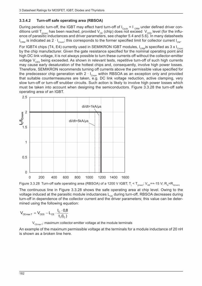
3 Datasheet Ratings for MOSFET, IGBT, Diodes and Thyristors
182
3.3.4.2 Turn-off safe operating area (RBSOA)
During periodic turn-off, the IGBT may effect hard turn-off of I Cpuls
= I CRM
under defi ned driver con-ditions until T
j(max) has been reached, provided V
CE (chip) does not exceed V
CES level (for the infl u-
ence of parasitic inductances and driver parameters, see chapter 5.4 and 5.6). In many datasheets I CRM
is indicated as 2 · I Cnom
; this corresponds to the former specifi ed limit for collector current I CM
.
For IGBT4 chips (T4, E4) currently used in SEMIKRON IGBT modules, I CRM
is specifi ed as 3 x I Cnom
by the chip manufacturer. Given the gate resistance specifi ed for the nominal operating point and high DC link voltage, it is not always possible to turn these currents off without the collector-emitter voltage V
CES being exceeded. As shown in relevant tests, repetitive turn-off of such high currents
may cause early desaturation of the hottest chips and, consequently, involve high power losses. Therefore, SEMIKRON recommends turning off currents above the permissible value specifi ed for the predecessor chip generation with 2 · I
Cnom within RBSOA as an exception only and provided
that suitable countermeasures are taken, e.g. DC link voltage reduction, active clamping, very slow turn-off or turn-off snubber circuits. Such action is likely to involve high power losses which must be taken into account when designing the semiconductors. Figure 3.3.28 the turn-off safe operating area of an IGBT.
0
0.5
1
1.5
2
2.5
0 200 400 600 800 1000 1200 1400 1600
I C/I
Cn
om
di/dt=5kA/µs
di/dt=1kA/µs
Figure 3.3.28 Turn-off safe operating area (RBSOA) of a 1200 V IGBT; T j < T
j(max) ; V
GE =+-15 V; R
G =R
G(nom)
The continuous line in Figure 3.3.28 shows the safe operating area at chip level. Owing to the voltage induced at the parasitic module inductances L
CE during turn-off, RBSOA decreases during
turn-off in dependence of the collector current and the driver parameters; this value can be deter-mined using the following equation:
)I(t
8,0ILVV
Cf
CCECESTmaxCE
××-=
V CEmax T
: maximum collector-emitter voltage at the module terminals
An example of the maximum permissible voltage at the terminals for a module inductance of 20 nH is shown as a broken line here.

3 Datasheet Ratings for MOSFET, IGBT, Diodes and Thyristors
183
3.3.4.3 Safe operating area during short circuit
Under certain conditions, the IGBT is essentially capable of turning off short circuits actively. In do-ing so, high power losses are generated by the IGBT working in the active operating area, causing a temporary increase in chip temperature to far beyond T
j(max) . However, the positive temperature
coeffi cient of the collector-emitter voltage causes the circuit to stabilise and the short-circuit cur-rent is limited to 4…6 · I
Cnom .
When turning off a short circuit, the high short-circuit current induces a voltage at the parasitic inductances in the commutation circuit; this voltage must not cause V
CES to be exceeded. In order
to limit the energy dissipation of the IGBT chips, short-circuit turn-off is subject to the following conditions: - The short circuit has to be detected and turned off within max. 10 µs (6 µs for 600 V Trench IGBT).
- The time between two short circuits has to be at least 1 second. - The IGBT must not be subjected to more than 1000 short circuits during its total operation time. - The maximum chip temperature before a short circuit occurs is limited to 150°C; this is also true for IGBT4 (T
j(max) = 175°C).
- The maximum voltage V CC
decreases, e.g. to 800 V for a 1200 V IGBT4. - The prevailing –di
c /dt maximum ratings must be controlled by the driver parameters and in ex-
treme cases, they can be achieved by means of multi-state turn-off only ("soft turn-off", cf. chap-ter 5.1.1).
- If necessary, non-permissible increase in gate-emitter voltage during short-circuit turn-off will have to be prevented by clamping.
Figure 3.3.29 gives an example of the dependency of the permissible short-circuit current I SC
(in relation to I
Cnom ) on the V
CE /V
CES ratio for a defi ned di/dt during turn-off. Here, too, it must be taken
into consideration that the voltage at the terminals is exceeded by the chip voltage to the amount of L
S · di/dt, meaning the maximum external voltage has to be reduced accordingly.
0
2
4
6
8
10
12
0 0.2 0.4 0.6 0.8 1 1.4V /VCE CES
I SC/I
Cn
om
T <= 150°Cj
V = +- 15VGE
di/dt<=2500A/µs
Figure 3.3.29 Safe operating area during short circuit (SCSOA)

3 Datasheet Ratings for MOSFET, IGBT, Diodes and Thyristors
184
3.4 Power MOSFET modules
When selecting MOSFET modules or comparing their properties using datasheet entries, it must be taken into account that the values given in the datasheets of different semiconductor manu-facturers are only comparable to a certain extent, because the specifi cation conditions may differ. In many cases, owing to the complex, application-specifi c interaction between different module features, additional measurements will be necessary.
Due to developments in the past decades, SEMIKRON datasheets are different with regards to the datasheet layout, data content and specifi cations for various generations of MOSFET modules and a variety of module designs. Since this data is to be standardised as part our product maintenance measures, the following information essentially refers to the latest datasheets issued in January 2010. Where applicable, different datasheet structures for the datasheets of older modules which are still being produced will be pointed out expressly. The basic datasheet layout is equivalent to that of IGBT modules introduced at the beginning of chapter 3.3.
Important data such as maximum ratings and characteristics valid for all different types of SEMI-KRON power MOSFET modules are not included in the type-specifi c datasheets, but are part of the "Technical Explanations" on the respective product range.
3.4.1 Maximum ratings
In the datasheets, the maximum ratings are specifi ed separately for each module component (or module function, such as forward conduction behaviour and negative conduction of MOSFET). All ratings refer to one switch, irrespective of the number of MOSFET chips per switch actually con-nected in parallel in the transistor module.
Figure 3.4.1 Datasheet excerpt: maximum ratings of a MOSFET module
3.4.1.1 Maximum forward ratings of power MOSFET
Drain-source voltage V DSS
Maximum voltage between the drain and source terminals of the MOSFET chips with gate-source short-circuited; parameters: case temperature T
c = 25°C, heatsink temperature for modules with-
out base plate T s = 25°C.
Owing to the temperature dependency of the breakdown voltage, the maximum drain-source vol-tage decreases in proportion to the temperature. Irrespective of the load conditions, the sum of the collector-emitter supply voltage V
DD and the switching overvoltage ∆V
DS = L
σ · di
D /dt must not ex-
ceed voltage V DSS
(L σ : sum of the parasitic inductance in the commutation circuit), cf. chapter 5.1.
3 Datasheet Ratings for MOSFET, IGBT, Diodes and Thyristors
185
Gate-source voltage V GSS
Maximum voltage between the gate and source terminals of the MOSFET chips; parameters: case temperature T
c = 25°C.
Continuous drain current I D
Maximum permissible continuous direct current over the collector output at which the permissible chip temperature is reached. Parameter: case temperature T
c = 25°C / 80°C, heatsink tempera-
ture T s = 25°C / 80°C for modules without base plate; for modules which can be soldered in PCBs
(SEMITOP) also maximum PCB temperature at the output terminals; chip temperature T j = T
j(max)
I D for modules with base plate is determined from
I D
2 = P tot(max)
/R DS(on)
mit P tot(max)
= (T j(max)
– T c )/R
th(j-c) ,
and for modules without base plate from
I D
2 = P tot(max)
/R DS(on)
mit P tot(max)
= (T j(max)
– T s )/R
th(j-s) .
Since I D designates a static maximum value, it is not relevant to switching operation.
Peak value of a pulsed drain current I DM
Peak value of current at the drain output during pulse operation; parameters: pulse duration t p ,
case temperature T c = 25°C or 80°C and pulse / break ratio.
Operating temperature range T j ; T
j(min) ....T
j(max)
Permissible IGBT chip temperature range for IGBT module operation; the chip temperature should be kept at least 25 K below T
j(max) , especially for permanent load conditions.
3.4.1.2 Maximum ratings of the inverse diodes (power MOSFET ratings in reverse direc-
tion)
Inverse diode forward current (continuous drain current in reverse direction) I F = -I
D
Maximum rated direct reverse current at drain output; maximum ratings and parameters are identi-cal to those for forward direction.
Repetitive peak forward current of the inverse diode I FM
= -I DM
Peak value of drain current during pulse operation; maximum ratings and parameters are identical to those in forward direction.
Operating temperature range T j ; T
j(min) ....T
j(max)
Permissible IGBT chip temperature range for IGBT module operation; the chip temperature should be kept at least 25 K below T
j(max) , especially under permanent load. The maximum ratings and
parameters correspond to those for forward direction.
3.4.1.3 Maximum module ratings
Storage temperature range T stg
; T stg(min)
....T stg(max)
Temperature range within which the module may be stored or transported without being subject to electrical load.
Soldering temperature T sol
for the output terminals (for modules with soldered terminals)
Maximum temperature to which the output terminals may be exposed when soldered onto a PCB; parameter: exposure time; see assembly instructions in chapter 6.3.4
Insulation test voltage V isol
Effective value of the permissible test voltage (50 Hz AC voltage) between the short-circuited terminals and insulated module base plate; parameter: test duration (1 min or 1 s); for details see chapter 5.1.1.2
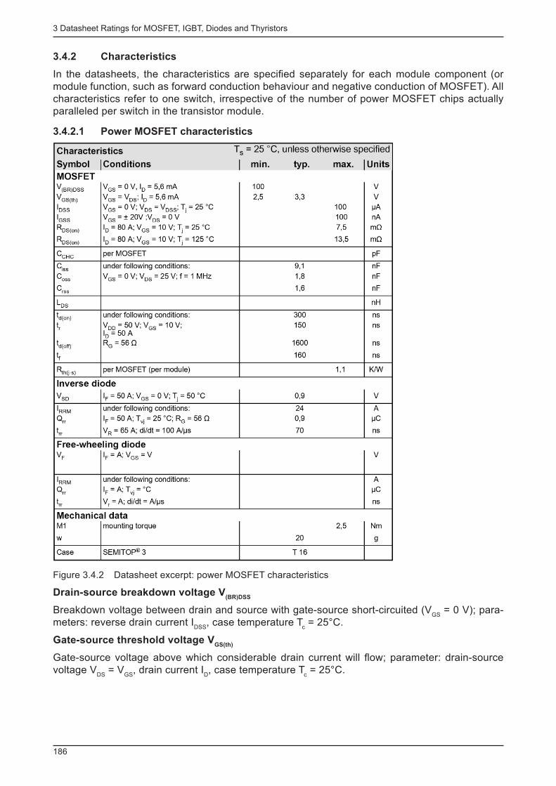
3 Datasheet Ratings for MOSFET, IGBT, Diodes and Thyristors
186
3.4.2 Characteristics
In the datasheets, the characteristics are specifi ed separately for each module component (or module function, such as forward conduction behaviour and negative conduction of MOSFET). All characteristics refer to one switch, irrespective of the number of power MOSFET chips actually paralleled per switch in the transistor module.
3.4.2.1 Power MOSFET characteristics
Figure 3.4.2 Datasheet excerpt: power MOSFET characteristics
Drain-source breakdown voltage V (BR)DSS
Breakdown voltage between drain and source with gate-source short-circuited (V GS
= 0 V); para-meters: reverse drain current I
DSS , case temperature T
c = 25°C.
Gate-source threshold voltage V GS(th)
Gate-source voltage above which considerable drain current will fl ow; parameter: drain-source voltage V
DS = V
GS , drain current I
D , case temperature T
c = 25°C.
3 Datasheet Ratings for MOSFET, IGBT, Diodes and Thyristors
187
Zero gate voltage drain current I DSS
Reverse current between drain and source with gate-source short-circuited (V GS
= 0 V) and maxi-mum drain-source voltage V
DS ; parameter: chip temperature, e.g. T
j = 25°C and 125°C; I
DSS rises
by a factor 3...6 at temperatures between 25°C and 125°C.
Gate-source leakage current I GSS
Leakage current between gate and source with drain-source short-circuited (V DS
= 0) and at maxi-mum gate-source voltage V
GS ; parameter: gate-source voltage V
GS = ±20 V.
Drain-source turn-on resistance R DS(on)
Quotient of changing drain-source voltage V DS
and drain current I D in a fully gate-controlled MOS-
FET at a specifi ed gate-source voltage V GS
and specifi ed drain current I D (i.e. at "rated current"); in
this forward state V DS
is proportional to I D , during large-signal behaviour the forward on-state vol-
tage V DS(on)
= R DS(on)
· I D
. Parameter: gate-source voltage V GS
= 20 V, drain current I D (i.e. "rated cur-
rent"), chip temperature T j = 25°C and 125°C (R
DS(on) is extremely dependent on the temperature!).
Capacitance chip-case (base plate) C CHC
Small signal capacitance between MOSFET chip and base plate with gate-source short-circuited; parameters: drain-source direct voltage V
DS , measuring frequency f = 1 MHz, case temperature T
c
= 25°C
Input capacitance C iss
, output capacitance C oss
, reverse transfer capacitance (Miller
capacitance) C rss
Small-signal capacitances defi ned in analogy to the IGBT low-signal capacitances; cf. chapter 3.3.2.
Parasitic drain-source inductance L DS
Inductance between drain and source, cf. chapter 3.3.2; parameters: drain-source direct voltage V
DS , case temperature T
c = 25°C.
Switching times t d(on)
, t r , t
d(off) , t
f
In contrast to IGBT, the switching times indicated in the datasheets of power MOSFET are deter-mined under less realistic conditions, using a measuring circuit under ohmic load, as shown in Figure 3.4.3. The defi nition of switching times refers to the gate-source voltage characteristics, cf. Figure 3.4.3b) and Figure 2.4.19 in chapter 2.4.3.2, as well as explanations concerning the physical background of current and voltage characteristics during switching. Parameters: supply voltage V
DD , continuous drain current I
D , gate control voltages V
GG+ , V
GG- (or V
GS ), external gate
resistances R Gon
, R Goff
, rate of rise of drain current +di D /dt during turn-on or rate of fall of drain cur-
rent -di D /dt during turn-off and chip temperature T
j (switching times and losses rising with junction
temperature).
What must be taken into consideration is that, in practice, switching times, current and voltage characteristics, as well as switching losses are largely determined by internal and external ca-pacitances, inductances and resistances in the gate and collector circuit. This means that ratings provided in the datasheet can often be taken as a rough guide only, meaning that additional mea-surements in the real application environment will inevitably have to be carried out to ensure safe layout of the circuitry.
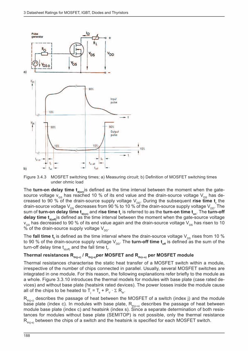
3 Datasheet Ratings for MOSFET, IGBT, Diodes and Thyristors
188
Figure 3.4.3 MOSFET switching times; a) Measuring circuit; b) Defi nition of MOSFET switching times under ohmic load
The turn-on delay time t d(on)
is defi ned as the time interval between the moment when the gate-source voltage v
GS has reached 10 % of its end value and the drain-source voltage V
DS has de-
creased to 90 % of the drain-source supply voltage V DD
. During the subsequent rise time t r the
drain-source voltage V DS
decreases from 90 % to 10 % of the drain-source supply voltage V DD
. The sum of turn-on delay time t
d(on) and rise time t
r is referred to as the turn-on time t
on . The turn-off
delay time t d(off)
is defi ned as the time interval between the moment when the gate-source voltage v
GS has decreased to 90 % of its end value again and the drain-source voltage V
DS has risen to 10
% of the drain-source supply voltage V DD
.
The fall time t f is defi ned as the time interval where the drain-source voltage V
DS rises from 10 %
to 90 % of the drain-source supply voltage V DD
. The turn-off time t off
is defi ned as the sum of the turn-off delay time t
d(off) and the fall time t
f .
Thermal resistances R th(j-c)
/ R th(j-s)
per MOSFET and R th(c-s)
per MOSFET module
Thermal resistances characterise the static heat transfer of a MOSFET switch within a module, irrespective of the number of chips connected in parallel. Usually, several MOSFET switches are integrated in one module. For this reason, the following explanations refer briefl y to the module as a whole. Figure 3.3.10 introduces the thermal models for modules with base plate (case rated de-vices) and without base plate (heatsink rated devices). The power losses inside the module cause all of the chips to be heated to T
j = T
a + P
V · Σ R
th .
R th(j-c)
describes the passage of heat between the MOSFET of a switch (index j) and the module base plate (index c). In modules with base plate, R
th(c-s) describes the passage of heat between
module base plate (index c) and heatsink (index s). Since a separate determination of both resis-tances for modules without base plate (SEMITOP) is not possible, only the thermal resistance R
th(j-s) between the chips of a switch and the heatsink is specifi ed for each MOSFET switch.
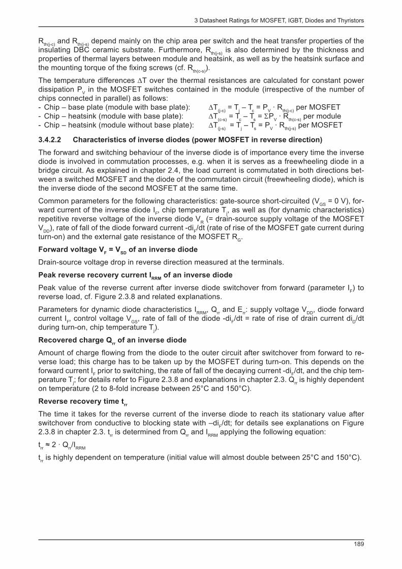
3 Datasheet Ratings for MOSFET, IGBT, Diodes and Thyristors
189
R th(j-c)
and R th(j-s)
depend mainly on the chip area per switch and the heat transfer properties of the insulating DBC ceramic substrate. Furthermore, R
th(j-s) is also determined by the thickness and
properties of thermal layers between module and heatsink, as well as by the heatsink surface and the mounting torque of the fi xing screws (cf. R
th(c-s) ).
The temperature differences ∆T over the thermal resistances are calculated for constant power dissipation P
V in the MOSFET switches contained in the module (irrespective of the number of
chips connected in parallel) as follows: - Chip – base plate (module with base plate): ∆T
(j-c) = T
j – T
c = P
V · R
th(j-c) per MOSFET
- Chip – heatsink (module with base plate): ∆T (c-s)
= T c – T
s = ΣP
V · R
th(c-s) per module
- Chip – heatsink (module without base plate): ∆T (j-s)
= T j – T
s = P
V · R
th(j-s) per MOSFET
3.4.2.2 Characteristics of inverse diodes (power MOSFET in reverse direction)
The forward and switching behaviour of the inverse diode is of importance every time the inverse diode is involved in commutation processes, e.g. when it is serves as a freewheeling diode in a bridge circuit. As explained in chapter 2.4, the load current is commutated in both directions bet-ween a switched MOSFET and the diode of the commutation circuit (freewheeling diode), which is the inverse diode of the second MOSFET at the same time.
Common parameters for the following characteristics: gate-source short-circuited (V GS
= 0 V), for-ward current of the inverse diode I
F , chip temperature T
j , as well as (for dynamic characteristics)
repetitive reverse voltage of the inverse diode V R (= drain-source supply voltage of the MOSFET
V DD
), rate of fall of the diode forward current -di F /dt (rate of rise of the MOSFET gate current during
turn-on) and the external gate resistance of the MOSFET R G .
Forward voltage V F = V
SD of an inverse diode
Drain-source voltage drop in reverse direction measured at the terminals.
Peak reverse recovery current I RRM
of an inverse diode
Peak value of the reverse current after inverse diode switchover from forward (parameter I F ) to
reverse load, cf. Figure 2.3.8 and related explanations.
Parameters for dynamic diode characteristics I RRM
, Q rr and E
rr : supply voltage V
DD , diode forward
current I F , control voltage V
GS , rate of fall of the diode -di
F /dt = rate of rise of drain current di
D /dt
during turn-on, chip temperature T j ).
Recovered charge Q rr of an inverse diode
Amount of charge fl owing from the diode to the outer circuit after switchover from forward to re-verse load; this charge has to be taken up by the MOSFET during turn-on. This depends on the forward current I
F prior to switching, the rate of fall of the decaying current -di
F /dt, and the chip tem-
perature T j ; for details refer to Figure 2.3.8 and explanations in chapter 2.3. Q
rr is highly dependent
on temperature (2 to 8-fold increase between 25°C and 150°C).
Reverse recovery time t rr
The time it takes for the reverse current of the inverse diode to reach its stationary value after switchover from conductive to blocking state with –di
F /dt; for details see explanations on Figure
2.3.8 in chapter 2.3. t rr is determined from Q
rr and I
RRM applying the following equation:
t rr ≈ 2 · Q
rr /I
RRM
t rr is highly dependent on temperature (initial value will almost double between 25°C and 150°C).

3 Datasheet Ratings for MOSFET, IGBT, Diodes and Thyristors
190
3.4.2.3 Mechanical module data
The following mechanical data is provided in the datasheets:
Mounting torque M1, M
s of the fi xing screws (minimum and maximum values),
Mounting torque M2, M
t of the terminals (minimum and maximum values),
Module weight w.
3.4.3 Diagrams
Following the sequence of the datasheets, this chapter provides information on the diagrams in MOSFET module datasheets, which normally refer to one partial-MOSFET or freewheeling diode. Some diagrams presented here are not shown in all of the datasheets of all module families, as some are specifi c to certain module families. In cases where the diagram concerned is detailed in other chapters, this will be referred to.
[Fig. 1] Rated power dissipation P D as a function of case temperature T
c
0
200
400
600
800
1000
0 50 100 150T °Cc
P
W
D
T 150 °Cj ≤
Figure 3.4.4 Maximum permissible power dissipation P D versus case temperature T
c
Based on the maximum permissible rated power dissipation per MOSFET, P D (25°C) = (T
j(max) –
25K)/R th(j-c)
at T c = 25°C, the function depicted in Figure 3.4.4 describes the power dissipation de-
rating in dependency of the case temperature.

3 Datasheet Ratings for MOSFET, IGBT, Diodes and Thyristors
191
[Fig. 2] Maximum permissible safe operating area during single-pulse operation (SOA)
1
10
100
1000
1 10 100 1000V VDS
I
AD
100 µs
1 ms
10 ms
T = 25 °CC
T 150 °Cj ≤
Not for
linear use
Figure 3.4.5 Safe operating area during single-pulse operation (SCSOA)
The MOSFET has to achieve an almost rectangular characteristic i= f(v) between V DD
and I L du-
ring hard switching. The SOA (Safe Operating Area) diagrams indicate to what extent this may be realised during different operating states without risk of destruction. The diagrams and limitations provided in chapter 3.3.4 apply here by analogy. MOSFET modules may only touch the linear cha-racteristic area during switching operation. Analogous operation over a longer period of time is not permitted, since asymmetries due to variation among the chips, as well as negative temperature coeffi cients of the threshold voltages might cause thermal instability.
[Fig. 3] Typical forward characteristics I D = f(V
DS ).
Figure 3.4.6 shows the output characteristic (typical values) based on the parameter V GS
(also see chapter 2.4.3).
0
100
200
300
400
500
0 2 4 6 8 1 0V VCC
7 V
6.5 V
6 V
5.5 V
5 V
4.5 V
4 V
8 V10 VV = 20 VGS
t = 80 sp μ
T = 25 °CjA
ID
Figure 3.4.6 Typical forward characteristics I D = f(V
DS )
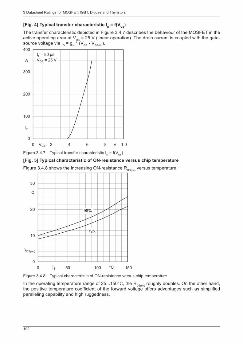
3 Datasheet Ratings for MOSFET, IGBT, Diodes and Thyristors
192
[Fig. 4] Typical transfer characteristic I D = f(V
GS )
The transfer characteristic depicted in Figure 3.4.7 describes the behaviour of the MOSFET in the active operating area at V
DS = 25 V (linear operation). The drain current is coupled with the gate-
source voltage via I D = g
fs * (V
GS - V
GS(th) ).
0
100
200
300
400
0 2 4 6 8 1 0V VGS
A
t = 80 sp μ
V = 25 VDS
ID
Figure 3.4.7 Typical transfer characteristic I D = f(V
GS )
[Fig. 5] Typical characteristic of ON-resistance versus chip temperature
Figure 3.4.8 shows the increasing ON-resistance R DS(on)
versus temperature.
0
10
20
30
0 50 100 150°C
Ω
98%
typ.
T
R
j
DS(on)
Figure 3.4.8 Typical characteristic of ON-resistance versus chip temperature
In the operating temperature range of 25...150°C, the R DS(on)
roughly doubles. On the other hand, the positive temperature coeffi cient of the forward voltage offers advantages such as simplifi ed paralleling capability and high ruggedness.
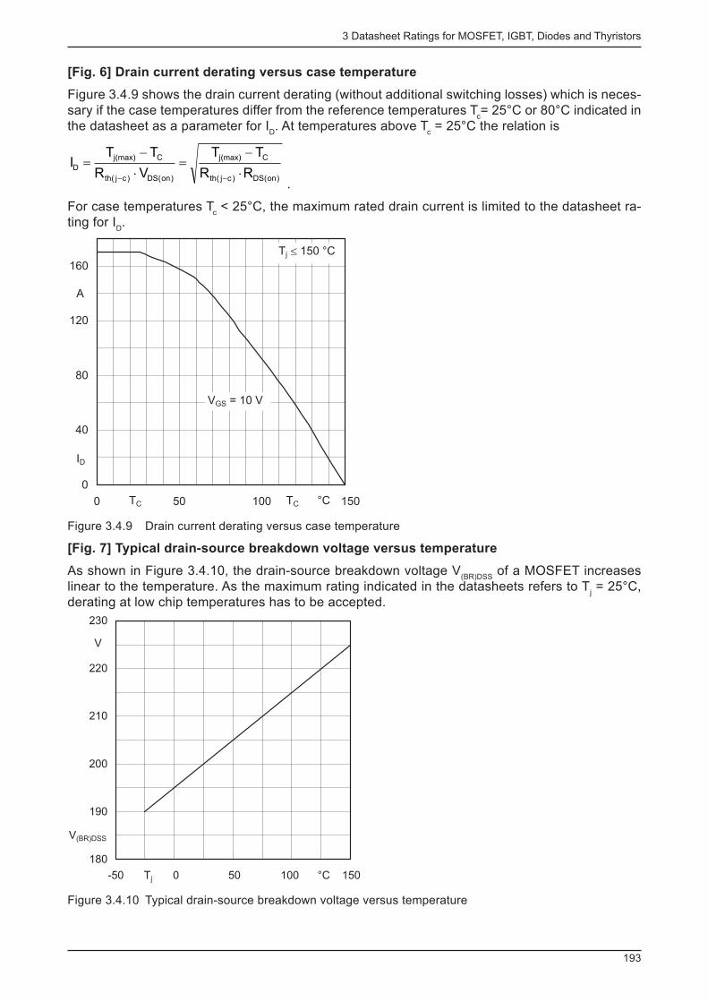
3 Datasheet Ratings for MOSFET, IGBT, Diodes and Thyristors
193
[Fig. 6] Drain current derating versus case temperature
Figure 3.4.9 shows the drain current derating (without additional switching losses) which is neces-sary if the case temperatures differ from the reference temperatures T
c = 25°C or 80°C indicated in
the datasheet as a parameter for I D . At temperatures above T
c = 25°C the relation is
)on(DS)cj(th
C(max)j
)on(DS)cj(th
C(max)j
DRR
TT
VR
TTI
×
-=
×
-=
-- .
For case temperatures T c < 25°C, the maximum rated drain current is limited to the datasheet ra-
ting for I D .
0
40
80
120
160
0 50 100 150T °CC
T 150 °Cj ≤
V = 10 VGS
A
T
I
C
D
Figure 3.4.9 Drain current derating versus case temperature
[Fig. 7] Typical drain-source breakdown voltage versus temperature
As shown in Figure 3.4.10, the drain-source breakdown voltage V (BR)DSS
of a MOSFET increases linear to the temperature. As the maximum rating indicated in the datasheets refers to T
j = 25°C,
derating at low chip temperatures has to be accepted.
180
190
200
210
220
230
-50 0 50 100 150
V
°CT
V
j
(BR)DSS
Figure 3.4.10 Typical drain-source breakdown voltage versus temperature
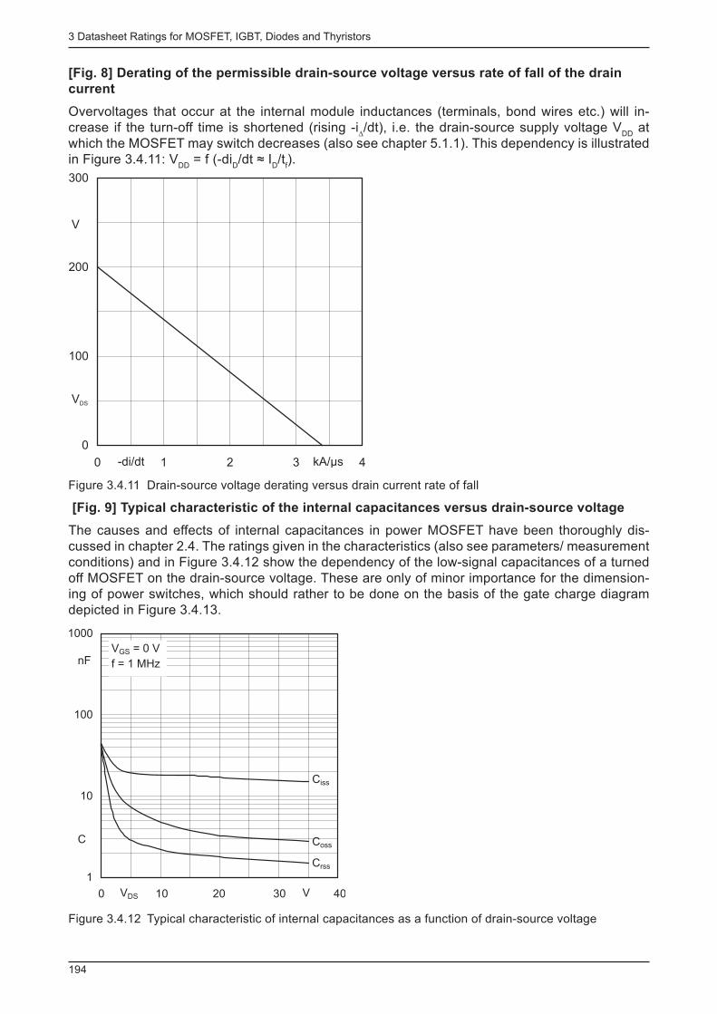
3 Datasheet Ratings for MOSFET, IGBT, Diodes and Thyristors
194
[Fig. 8] Derating of the permissible drain-source voltage versus rate of fall of the drain
current
Overvoltages that occur at the internal module inductances (terminals, bond wires etc.) will in-crease if the turn-off time is shortened (rising -i
∆ /dt), i.e. the drain-source supply voltage V
DD at
which the MOSFET may switch decreases (also see chapter 5.1.1). This dependency is illustrated in Figure 3.4.11: V
DD = f (-di
D /dt ≈ I
D /t
f ).
0
100
200
300
0 1 2 3 4-di/dt
V
kA/μs
VDS
Figure 3.4.11 Drain-source voltage derating versus drain current rate of fall
[Fig. 9] Typical characteristic of the internal capacitances versus drain-source voltage
The causes and effects of internal capacitances in power MOSFET have been thoroughly dis-cussed in chapter 2.4. The ratings given in the characteristics (also see parameters/ measurement conditions) and in Figure 3.4.12 show the dependency of the low-signal capacitances of a turned off MOSFET on the drain-source voltage. These are only of minor importance for the dimension-ing of power switches, which should rather to be done on the basis of the gate charge diagram depicted in Figure 3.4.13.
1
10
100
1000
0 V
nF
C
C
C
iss
oss
rss
V = 0 VGS
f = 1 MHz
C
VDS 10 20 30 40
Figure 3.4.12 Typical characteristic of internal capacitances as a function of drain-source voltage
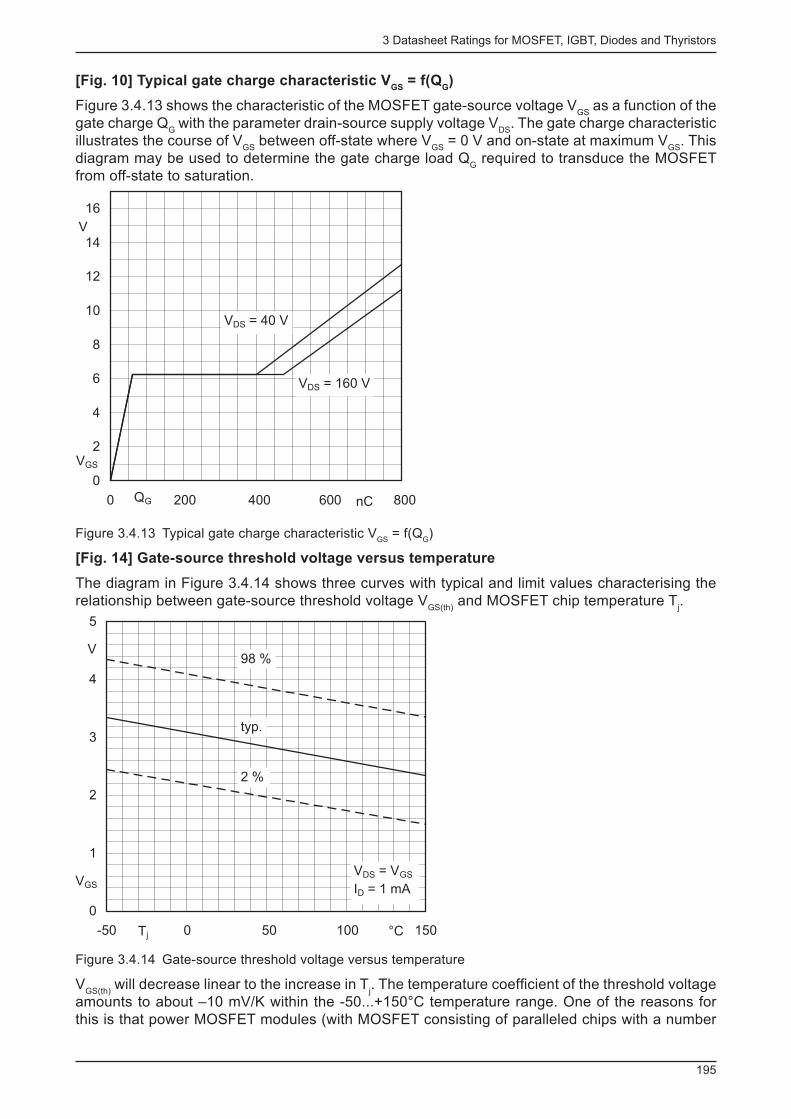
3 Datasheet Ratings for MOSFET, IGBT, Diodes and Thyristors
195
[Fig. 10] Typical gate charge characteristic V GS
= f(Q G )
Figure 3.4.13 shows the characteristic of the MOSFET gate-source voltage V GS
as a function of the gate charge Q
G with the parameter drain-source supply voltage V
DS . The gate charge characteristic
illustrates the course of V GS
between off-state where V GS
= 0 V and on-state at maximum V GS
. This diagram may be used to determine the gate charge load Q
G required to transduce the MOSFET
from off-state to saturation.
0
2
4
6
8
10
12
14
16
0 200 400 600 800nC
V
V = 160 VDS
V = 40 VDS
VGS
QG
Figure 3.4.13 Typical gate charge characteristic V GS
= f(Q G )
[Fig. 14] Gate-source threshold voltage versus temperature
The diagram in Figure 3.4.14 shows three curves with typical and limit values characterising the relationship between gate-source threshold voltage V
GS(th) and MOSFET chip temperature T
j .
0
1
2
3
4
5
-50 0 50 100 150
V98 %
typ.
2 %
V = V
I = 1 mADS GS
D
°C
V
T
GS
j
Figure 3.4.14 Gate-source threshold voltage versus temperature
V GS(th)
will decrease linear to the increase in T j . The temperature coeffi cient of the threshold voltage
amounts to about –10 mV/K within the -50...+150°C temperature range. One of the reasons for this is that power MOSFET modules (with MOSFET consisting of paralleled chips with a number
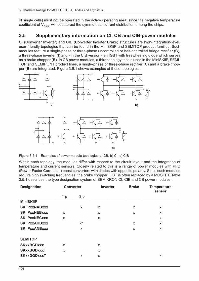
3 Datasheet Ratings for MOSFET, IGBT, Diodes and Thyristors
196
of single cells) must not be operated in the active operating area, since the negative temperature coeffi cient of V
GS(th) will counteract the symmetrical current distribution among the chips.
3.5 Supplementary information on CI, CB and CIB power modules
CI ( C onverter I nverter) and CIB ( C onverter I nverter B rake) structures are high-integration-level, user-friendly topologies that can be found in the MiniSKiiP and SEMITOP product families. Such modules feature a single-phase or three-phase uncontrolled or half-controlled bridge rectifi er ( C ), a three-phase inverter ( I ) and - in the CIB version - an IGBT with freewheeling diode which serves as a brake chopper ( B ). In CB power modules, a third topology that is used in the MiniSKiiP, SEMI-TOP and SEMIPONT product lines, a single-phase or three-phase rectifi er ( C ) and a brake chop-per ( B ) are integrated. Figure 3.5.1 shows examples of these topologies.
b)a)
c)
Figure 3.5.1 Examples of power module topologies a) CB, b) CI, c) CIB
Within each topology, the modules differ with respect to the circuit layout and the integration of temperature and current sensors. Closely related to this is a range of power modules with PFC ( P ower F actor C orrection) boost converters with diodes with opposite polarity. Since such modules require high switching frequencies, the brake chopper IGBT is often replaced by a MOSFET. Table 3.5.1 describes the type designation system of SEMIKRON CI, CIB and CB power modules.
Designation Converter Inverter Brake Temperature
sensor
1-p 3-p
MiniSKiiP
SKiiPxxNABxxx x x x x
SKiiPxxNEBxxx x x x x
SKiiPxxNECxxx x x x
SKiiPxxAHBxxx x* x x
SKiiPxxANBxxx x x x
SEMITOP
SKxxBGDxxx x x
SKxxBGDxxxT x x
SKxxDGDxxxT x x x

3 Datasheet Ratings for MOSFET, IGBT, Diodes and Thyristors
197
Designation Converter Inverter Brake Temperature
sensor
1-p 3-p
SKxxDGDLxxxT x x x x
SKxxDGLxxx x x x
SKxxDHLxxx x* x
SEMIPONT
SKDxxx/xxLxx x x x
SKDHxxx/xxLxx x*
* half-controlled rectifi er bridge
Table 3.5.1 Type designation system of SEMIKRON CI, CIB and CB power modules
The datasheet ratings for inverter and brake chopper IGBT and diodes, the temperature sensor and the properties of CI, CIB and CB power modules correspond to those for IGBT modules pro-vided in chapter 3.3. The same freewheeling diodes are used for inverters and brake choppers, whereas the chopper IGBT of some CIB modules may be smaller than the inverter IGBT. In such cases, the datasheet of another module type may be referred to in the relevant datasheet (Figure 3.5.2).
Figure 3.5.2 Datasheet excerpt with maximum ratings and characteristics of a SK50DGDL12T4 CIB module
The properties of rectifi er diodes or thyristors are also given in the datasheet tables and diagrams. Explanations on the respective maximum ratings, characteristics and diagrams are included in the chapters 3.1...3.4.
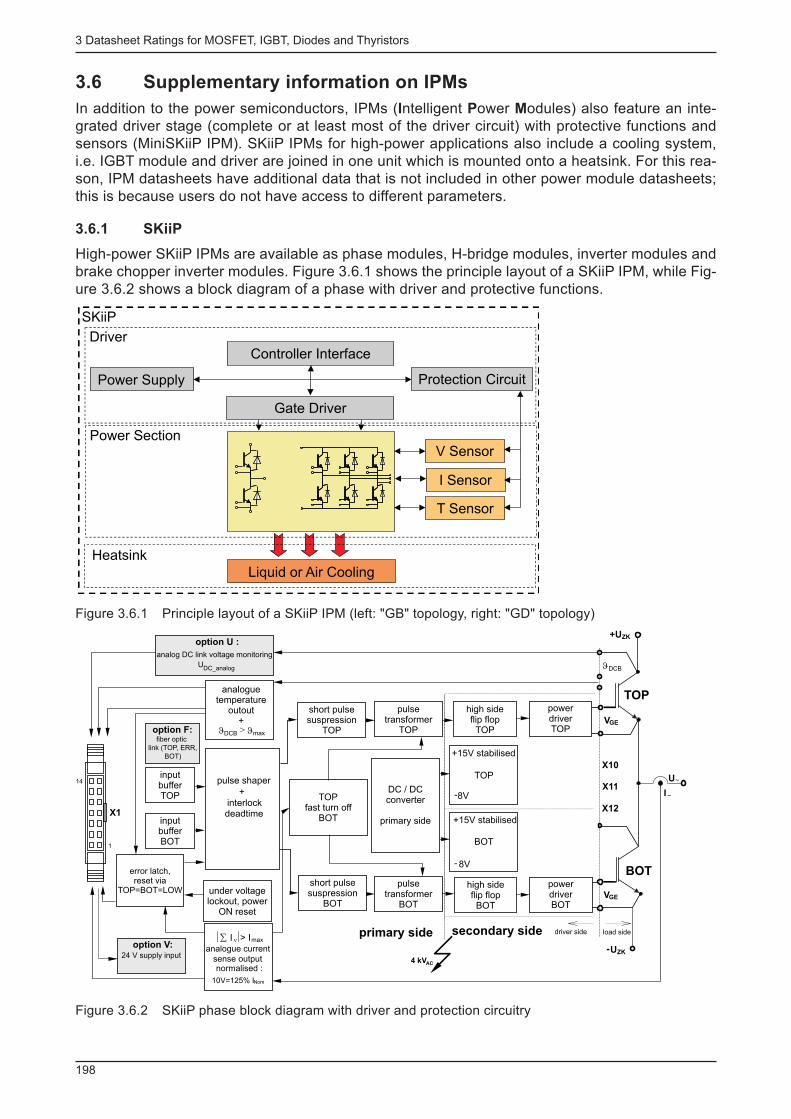
3 Datasheet Ratings for MOSFET, IGBT, Diodes and Thyristors
198
3.6 Supplementary information on IPMs
In addition to the power semiconductors, IPMs ( I ntelligent P ower M odules) also feature an inte-grated driver stage (complete or at least most of the driver circuit) with protective functions and sensors (MiniSKiiP IPM). SKiiP IPMs for high-power applications also include a cooling system, i.e. IGBT module and driver are joined in one unit which is mounted onto a heatsink. For this rea-son, IPM datasheets have additional data that is not included in other power module datasheets; this is because users do not have access to different parameters.
3.6.1 SKiiP
High-power SKiiP IPMs are available as phase modules, H-bridge modules, inverter modules and brake chopper inverter modules. Figure 3.6.1 shows the principle layout of a SKiiP IPM, while Fig-ure 3.6.2 shows a block diagram of a phase with driver and protective functions.
V Sensor
I Sensor
T Sensor
Liquid or Air Cooling
Gate Driver
Controller Interface
Protection CircuitPower Supply
SKiiP
Power Section
Driver
Heatsink
Figure 3.6.1 Principle layout of a SKiiP IPM (left: "GB" topology, right: "GD" topology)
under voltagelockout, power
ON reset
TOPfast turn off
BOT
pulsetransformer
BOT
+15V stabilised
TOP
-8VDC / DCconverter
primary side +15V stabilised
BOT
- 8V
pulse shaper
+
interlockdeadtime
analoguetemperature
outout+
JDCB > Jmax
error latch,reset via
TOP=BOT=LOW
inputbufferBOT
inputbufferTOP
option V:24 V supply input
X1
14
1
powerdriverTOP
powerdriverBOT
-UZK
load side
VGE
VGE
+UZK
U~
I~
JDCB
X10
X11
X12
driver side
high sideflip flop
TOP
high sideflip flop
BOT
short pulsesuspression
BOT
secondary sideprimary side½å I n½> Imax
analogue current
sense outputnormalised :
10V=125% INom
TOP
BOT
4 kVAC
option U :
analog DC link voltage monitoring
UDC_analog
option F:fiber optic
link (TOP, ERR,
BOT)
pulsetransformer
TOP
short pulsesuspression
TOP
Figure 3.6.2 SKiiP phase block diagram with driver and protection circuitry

3 Datasheet Ratings for MOSFET, IGBT, Diodes and Thyristors
199
Three SKiiP generations are available at present: SKiiP2 with NPT-IGBT, SKiiP3 with Trench IGBT3 and SKiiP4 with Trench IGBT4. All SKiiP modules contain 2 to 4 (for SKiiP4 even 6) identi-cal half bridges ("folds") mounted in a line on a heatsink with IGBT and diodes for either 1200 V or 1700 V reverse voltage. Figure 3.6.3 shows the range of circuit topologies: "GB" (half bridge), "GH" (2-phase H-bridge), "GD" (3-phase inverter) and "GDL" (3-phase inverter with brake chop-per).
Driver
+
-
~
SKiiP: 2-fold "GB" (Case S2; S23)
Driver
+
-
~
SKiiP: 3-fold "GB" (Case S3; S33)
SKiiP: 4-fold "GB" (Case S4; S43)
+
-
~
Driver
SKiiP: 3-fold "GD" (Case S3; S33)
Driver
+
-
UVW
only SKiiP2: 4-fold "GH" (Case S5GH) only SKiiP2: 4-fold "GDL" (Case S5GDL)
+
-
U
V
Driver Driver
+
-
UVWBR
DriverDriver
Driver
+
-
~
only SKiiP4: 6-fold "GB"
Figure 3.6.3 SKiiP topologies

3 Datasheet Ratings for MOSFET, IGBT, Diodes and Thyristors
200
Although the half bridges are controlled by a common driver, each half bridge is equipped with separate power terminals (DC+, AC, DC-) for connection at the customer's site (see example in Figure 3.6.4).
Figure 3.6.4 Power terminals of a SKiiP3
To guarantee optimal performance of SKiiP modules, the "Technical Explanations" provided for all SKiiP modules under www.semikron.com must be adhered to in addition to the type-specifi c data in the datasheets. Figure 3.6.5 gives an example of the basic datasheet layout of SKiiP modules.
Figure 3.6.5 Datasheet layout for SKiiP modules
Unlike the datasheets for conventional power modules, SKiiP datasheets do not contain diagrams. In addition to the designation and a photo of the module, page 1 contains a description of the power section, as well as the respective maximum ratings and characteristics in the form of tables. The characteristics are divided into minimum, typical and maximum values. General information on the chip technology used and the integrated components is given in the shaded area to the left

3 Datasheet Ratings for MOSFET, IGBT, Diodes and Thyristors
201
of the maximum ratings and characteristics. Furthermore, this section provides information on cli-mate classes, UL listing, explanations on footnotes, and a circuit diagram of the SKiiP module. The datasheet date of issue is given on all pages in the shaded footer. Page 2 features the maximum ratings and characteristics of the driver circuit. The greyed-out section provides additional driver properties and possible options.
3.6.1.1 Maximum ratings of the power section
In SKiiP datasheets, the maximum ratings are specifi ed separately for the power section and the driver. All ratings for IGBT and diodes refer to one switch (arm), irrespective of the number of paralleled IGBT or diode chips per switch (arm) in the transistor module. The maximum ratings indicated in chapter 3.3 apply to IGBT and diodes.
DC link supply voltage V CC
Parameter: heatsink temperature T s = 25°C; maximum DC supply voltage applied between the DC
terminals in a SKiiP module. This maximum rating will be applicable provided that the DC termi-nals are connected to adequate high-frequency (MKP) snubber capacitors (for selection refer to "Technical Explanations" and [AN1]).
If the DC and AC busbar system has a suffi ciently minimal low-inductance design, the SKiiP mo-dule will be able to turn off short-circuits within the rated DC supply voltage range without that V
CES is exceeded across the chips. Information on the key busbar system properties and de-
sign are also included in the Technical Explanations and the application notes retrievable under www.semikron.com. V
CC may be exceeded briefl y only and up to a maximum value of V
CES even
for blocked IGBT.
RMS on-state current I AC terminal
, I t(RMS)
Maximum current load applied to the power terminals of a half-bridge (fold) I AC-terminal
, which cor-responds to I
t(RMS) of an IGBT module (see chapter 3.3.1); parameter: heatsink temperature T
s =
70°C. Since the terminal temperature affects the operating temperature of the SKiiP driver, the maximum terminal temperature T
terminal (< 115°C) is also given as a parameter.
3.6.1.2 Maximum ratings of a SKiiP driver
Figure 3.6.6 Datasheet excerpt: maximum ratings of a SKiiP driver
Driver supply voltage V s2
Absolute maximum unstabilised supply voltage of the SKiiP driver.
Input signal voltage (HIGH) V i
The maximum input signal voltage is derived from the high-level specifi cation of the driver logic used to form the input signal.
Rate of rise of voltage on the secondary side dv/dt
Maximum rate of rise of voltage on the secondary side (power side) during IGBT switching under which the driver can still operate uninhibited.
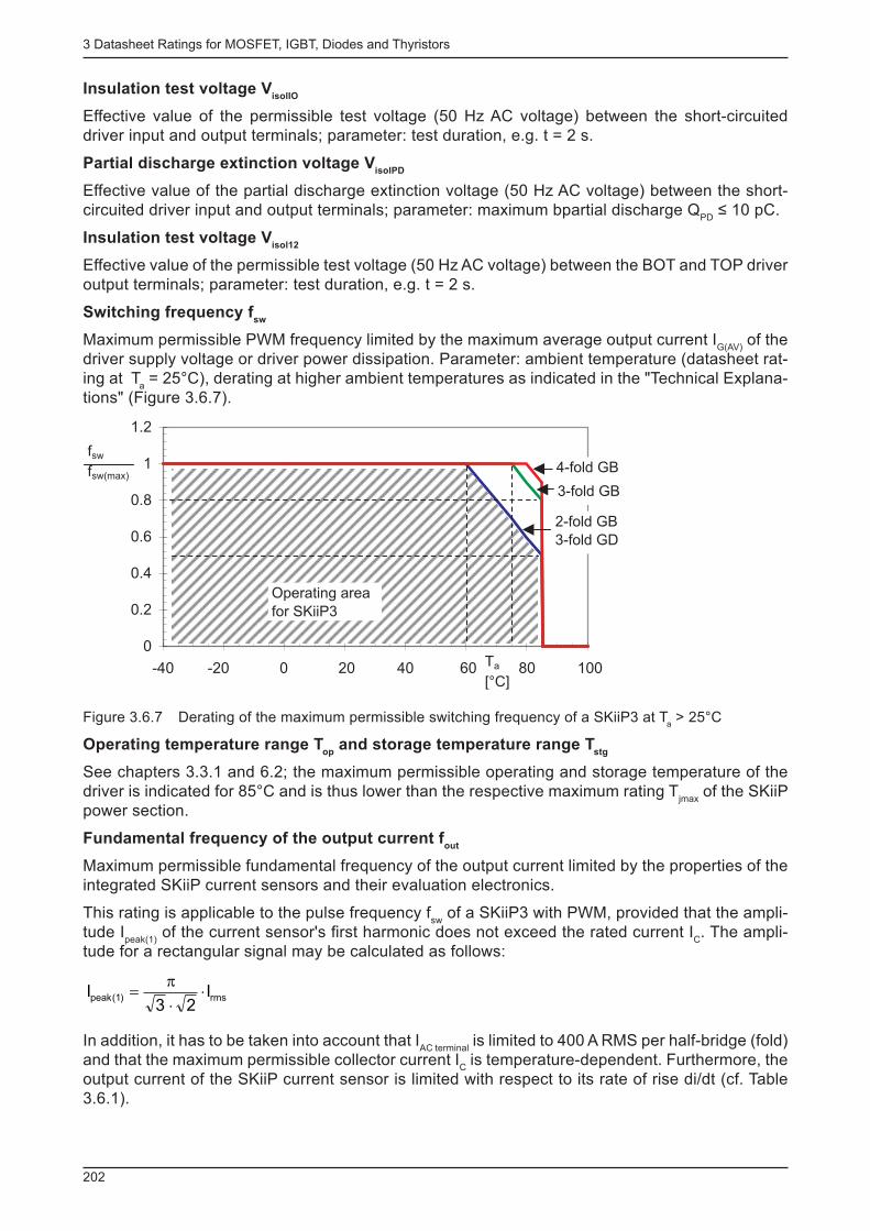
3 Datasheet Ratings for MOSFET, IGBT, Diodes and Thyristors
202
Insulation test voltage V isolIO
Effective value of the permissible test voltage (50 Hz AC voltage) between the short-circuited driver input and output terminals; parameter: test duration, e.g. t = 2 s.
Partial discharge extinction voltage V isolPD
Effective value of the partial discharge extinction voltage (50 Hz AC voltage) between the short-circuited driver input and output terminals; parameter: maximum bpartial discharge Q
PD ≤ 10 pC.
Insulation test voltage V isol12
Effective value of the permissible test voltage (50 Hz AC voltage) between the BOT and TOP driver output terminals; parameter: test duration, e.g. t = 2 s.
Switching frequency f sw
Maximum permissible PWM frequency limited by the maximum average output current I G(AV)
of the driver supply voltage or driver power dissipation. Parameter: ambient temperature (datasheet rat-ing at T
a = 25°C), derating at higher ambient temperatures as indicated in the "Technical Explana-
tions" (Figure 3.6.7).
0
0.2
0.4
0.6
0.8
1
1.2
-40 -20 0 20 40 60 80 100
fsw
fsw(max)
Ta
[°C]
4-fold GB
3-fold GB
2-fold GB
3-fold GD
Operating area
for SKiiP3
Figure 3.6.7 Derating of the maximum permissible switching frequency of a SKiiP3 at T a > 25°C
Operating temperature range T op
and storage temperature range T stg
See chapters 3.3.1 and 6.2; the maximum permissible operating and storage temperature of the driver is indicated for 85°C and is thus lower than the respective maximum rating T
jmax of the SKiiP
power section.
Fundamental frequency of the output current f out
Maximum permissible fundamental frequency of the output current limited by the properties of the integrated SKiiP current sensors and their evaluation electronics.
This rating is applicable to the pulse frequency f sw
of a SKiiP3 with PWM, provided that the ampli-tude I
peak(1) of the current sensor's fi rst harmonic does not exceed the rated current I
C . The ampli-
tude for a rectangular signal may be calculated as follows:
rms)1(peak I
23I ×
×p
=
In addition, it has to be taken into account that I AC terminal
is limited to 400 A RMS per half-bridge (fold) and that the maximum permissible collector current I
C is temperature-dependent. Furthermore, the
output current of the SKiiP current sensor is limited with respect to its rate of rise di/dt (cf. Table 3.6.1).
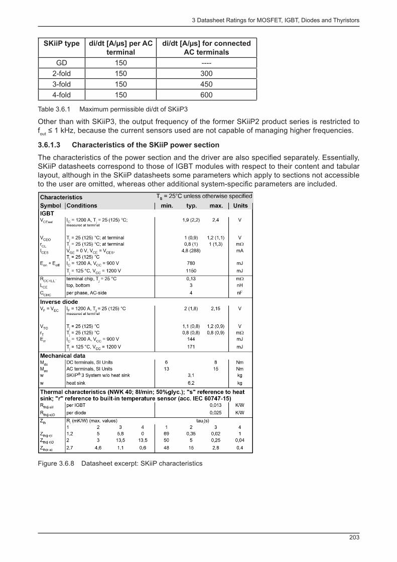
3 Datasheet Ratings for MOSFET, IGBT, Diodes and Thyristors
203
SKiiP type di/dt [A/µs] per AC
terminal
di/dt [A/µs] for connected
AC terminals
GD 150 ----
2-fold 150 300
3-fold 150 450
4-fold 150 600
Table 3.6.1 Maximum permissible di/dt of SKiiP3
Other than with SKiiP3, the output frequency of the former SKiiP2 product series is restricted to f out
≤ 1 kHz, because the current sensors used are not capable of managing higher frequencies.
3.6.1.3 Characteristics of the SKiiP power section
The characteristics of the power section and the driver are also specifi ed separately. Essentially, SKiiP datasheets correspond to those of IGBT modules with respect to their content and tabular layout, although in the SKiiP datasheets some parameters which apply to sections not accessible to the user are omitted, whereas other additional system-specifi c parameters are included.
Figure 3.6.8 Datasheet excerpt: SKiiP characteristics
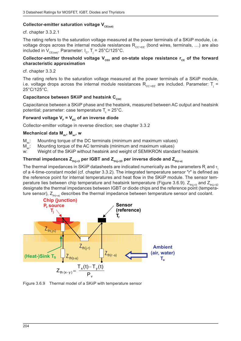
3 Datasheet Ratings for MOSFET, IGBT, Diodes and Thyristors
204
Collector-emitter saturation voltage V CE(sat)
cf. chapter 3.3.2.1
The rating refers to the saturation voltage measured at the power terminals of a SKiiP module, i.e. voltage drops across the internal module resistances R
CC’+EE’ (bond wires, terminals, …) are also
included in V CE(sat)
. Parameter: I C , T
j = 25°C/125°C.
Collector-emitter threshold voltage V CE0
and on-state slope resistance r CE
of the forward
characteristic approximation
cf. chapter 3.3.2
The rating refers to the saturation voltage measured at the power terminals of a SKiiP module, i.e. voltage drops across the internal module resistances R
CC’+EE’ are included. Parameter: T
j =
25°C/125°C.
Capacitance between SKiiP and heatsink C CHC
Capacitance between a SKiiP phase and the heatsink, measured between AC output and heatsink potential; parameter: case temperature T
c = 25°C.
Forward voltage V F = V
EC of an inverse diode
Collector-emitter voltage in reverse direction; see chapter 3.3.2
Mechanical data M dc
, M ac
, w
M dc
: Mounting torque of the DC terminals (minimum and maximum values) M
ac : Mounting torque of the AC terminals (minimum and maximum values)
w: Weight of the SKiiP without heatsink and weight of SEMIKRON standard heatsink
Thermal impedances Z th(j-r)I
per IGBT and Z th(j-r)D
per inverse diode and Z th(r-a)
The thermal impedances in SKiiP datasheets are indicated numerically as the parameters R i and τ
i
of a 4-time-constant model (cf. chapter 3.3.2). The integrated temperature sensor "r" is defi ned as the reference point for internal temperatures and heat fl ow in the SKiiP module. The sensor tem-perature lies between chip temperature and heatsink temperature (Figure 3.6.9). Z
th(j-r)I and Z
th(j-r)D
designate the thermal impedances between IGBT or diode chips and the reference point (tempera-ture sensor), Z
th(r-a) describes the thermal impedance between temperature sensor and coolant.
Ambient
(air, water)Ta
Chip (junction)Pv source
Tj
(Heat-)Sink TS Z th(s-a)
Z th( j-s)
Sensor(reference)Tr
Zth(r -a)
Zth(j-r)
v
yx)yx(th
P
)t(T)t(TZ
-=-
Figure 3.6.9 Thermal model of a SKiiP with temperature sensor
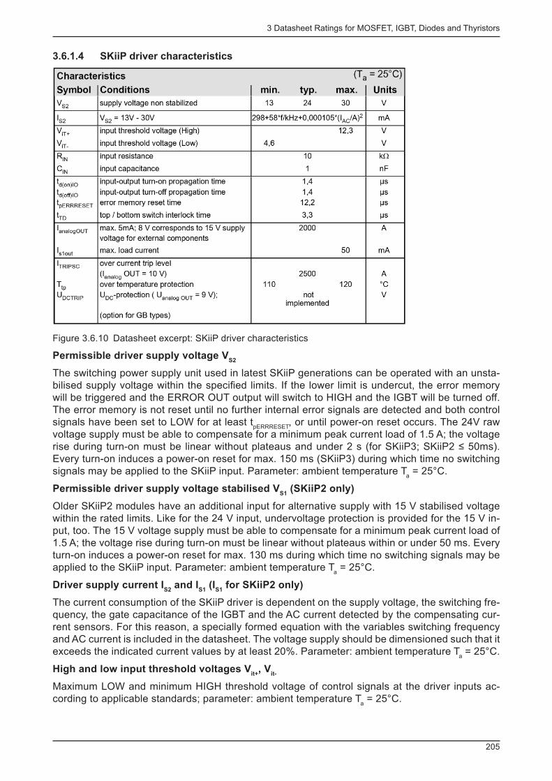
3 Datasheet Ratings for MOSFET, IGBT, Diodes and Thyristors
205
3.6.1.4 SKiiP driver characteristics
Figure 3.6.10 Datasheet excerpt: SKiiP driver characteristics
Permissible driver supply voltage V S2
The switching power supply unit used in latest SKiiP generations can be operated with an unsta-bilised supply voltage within the specifi ed limits. If the lower limit is undercut, the error memory will be triggered and the ERROR OUT output will switch to HIGH and the IGBT will be turned off. The error memory is not reset until no further internal error signals are detected and both control signals have been set to LOW for at least t
pERRRESET , or until power-on reset occurs. The 24V raw
voltage supply must be able to compensate for a minimum peak current load of 1.5 A; the voltage rise during turn-on must be linear without plateaus and under 2 s (for SKiiP3; SKiiP2 ≤ 50ms). Every turn-on induces a power-on reset for max. 150 ms (SKiiP3) during which time no switching signals may be applied to the SKiiP input. Parameter: ambient temperature T
a = 25°C.
Permissible driver supply voltage stabilised V S1
(SKiiP2 only)
Older SKiiP2 modules have an additional input for alternative supply with 15 V stabilised voltage within the rated limits. Like for the 24 V input, undervoltage protection is provided for the 15 V in-put, too. The 15 V voltage supply must be able to compensate for a minimum peak current load of 1.5 A; the voltage rise during turn-on must be linear without plateaus within or under 50 ms. Every turn-on induces a power-on reset for max. 130 ms during which time no switching signals may be applied to the SKiiP input. Parameter: ambient temperature T
a = 25°C.
Driver supply current I S2
and I S1
(I S1
for SKiiP2 only)
The current consumption of the SKiiP driver is dependent on the supply voltage, the switching fre-quency, the gate capacitance of the IGBT and the AC current detected by the compensating cur-rent sensors. For this reason, a specially formed equation with the variables switching frequency and AC current is included in the datasheet. The voltage supply should be dimensioned such that it exceeds the indicated current values by at least 20%. Parameter: ambient temperature T
a = 25°C.
High and low input threshold voltages V it+
, V it-
Maximum LOW and minimum HIGH threshold voltage of control signals at the driver inputs ac-cording to applicable standards; parameter: ambient temperature T
a = 25°C.
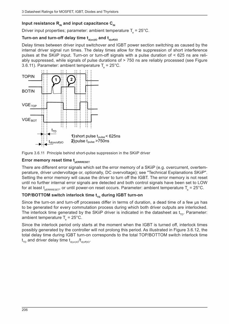
3 Datasheet Ratings for MOSFET, IGBT, Diodes and Thyristors
206
Input resistance R IN
and input capacitance C IN
Driver input properties; parameter: ambient temperature T a = 25°C.
Turn-on and turn-off delay time t d(on)IO
and t d(off)IO
Delay times between driver input switchover and IGBT power section switching as caused by the internal driver signal run times. The delay times allow for the suppression of short interference pulses at the SKiiP input. Turn-on or turn-off signals with a pulse duration of < 625 ns are reli-ably suppressed, while signals of pulse durations of > 750 ns are reliably processed (see Figure 3.6.11). Parameter: ambient temperature T
a = 25°C.
TOPIN
BOTIN
VGETOP
VGEBOT
td(on/off)IO
tTD
1 2
1)short pulse tpulse< 625ns2)pulse tpulse >750ns
Figure 3.6.11 Principle behind short-pulse suppression in the SKiiP driver
Error memory reset time t pERRRESET
There are different error signals which set the error memory of a SKiiP (e.g. overcurrent, overtem-perature, driver undervoltage or, optionally, DC overvoltage); see "Technical Explanations SKiiP". Setting the error memory will cause the driver to turn off the IGBT. The error memory is not reset until no further internal error signals are detected and both control signals have been set to LOW for at least t
pERRRESET , or until power-on reset occurs. Parameter: ambient temperature T
a = 25°C.
TOP/BOTTOM switch interlock time t TD
during IGBT turn-on
Since the turn-on and turn-off processes differ in terms of duration, a dead time of a few µs has to be generated for every commutation process during which both driver outputs are interlocked. The interlock time generated by the SKiiP driver is indicated in the datasheet as t
TD . Parameter:
ambient temperature T a = 25°C.
Since the interlock period only starts at the moment when the IGBT is turned off, interlock times possibly generated by the controller will not prolong this period. As illustrated in Figure 3.6.12, the total delay time during IGBT turn-on corresponds to the total TOP/BOTTOM switch interlock time t TD
and driver delay time t d(on)IO
/t d(off)IO
.
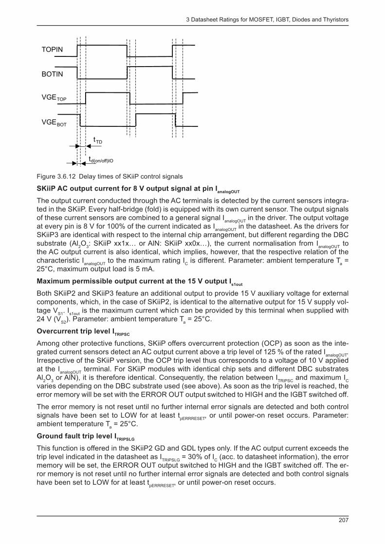
3 Datasheet Ratings for MOSFET, IGBT, Diodes and Thyristors
207
TOPIN
BOTIN
VGETOP
VGEBOT
td(on/off)IO
tTD
Figure 3.6.12 Delay times of SKiiP control signals
SKiiP AC output current for 8 V output signal at pin I analogOUT
The output current conducted through the AC terminals is detected by the current sensors integra-ted in the SKiiP. Every half-bridge (fold) is equipped with its own current sensor. The output signals of these current sensors are combined to a general signal I
analogOUT in the driver. The output voltage
at every pin is 8 V for 100% of the current indicated as I analogOUT
in the datasheet. As the drivers for SKiiP3 are identical with respect to the internal chip arrangement, but different regarding the DBC substrate (Al
2 O
3 : SKiiP xx1x… or AlN: SKiiP xx0x…), the current normalisation from I
analogOUT to
the AC output current is also identical, which implies, however, that the respective relation of the characteristic I
analogOUT to the maximum rating I
C is different. Parameter: ambient temperature T
a =
25°C, maximum output load is 5 mA.
Maximum permissible output current at the 15 V output I s1out
Both SKiiP2 and SKiiP3 feature an additional output to provide 15 V auxiliary voltage for external components, which, in the case of SKiiP2, is identical to the alternative output for 15 V supply vol-tage V
S1 . I
s1out is the maximum current which can be provided by this terminal when supplied with
24 V (V S2
). Parameter: ambient temperature T a = 25°C.
Overcurrent trip level I TRIPSC
Among other protective functions, SKiiP offers overcurrent protection (OCP) as soon as the inte-grated current sensors detect an AC output current above a trip level of 125 % of the rated I
analogOUT .
Irrespective of the SKiiP version, the OCP trip level thus corresponds to a voltage of 10 V applied at the I
analogOUT terminal. For SKiiP modules with identical chip sets and different DBC substrates
Al 2 O
3 or AlN), it is therefore identical. Consequently, the relation between I
TRIPSC and maximum I
C
varies depending on the DBC substrate used (see above). As soon as the trip level is reached, the error memory will be set with the ERROR OUT output switched to HIGH and the IGBT switched off.
The error memory is not reset until no further internal error signals are detected and both control signals have been set to LOW for at least t
pERRRESET , or until power-on reset occurs. Parameter:
ambient temperature T a = 25°C.
Ground fault trip level I TRIPSLG
This function is offered in the SKiiP2 GD and GDL types only. If the AC output current exceeds the trip level indicated in the datasheet as I
TRIPSLG = 30% of I
C (acc. to datasheet information), the error
memory will be set, the ERROR OUT output switched to HIGH and the IGBT switched off. The er-ror memory is not reset until no further internal error signals are detected and both control signals have been set to LOW for at least t
pERRRESET , or until power-on reset occurs.
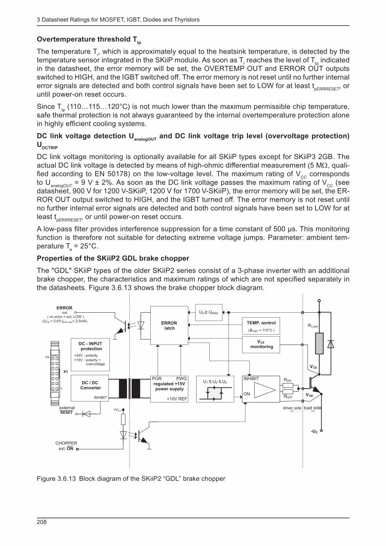
3 Datasheet Ratings for MOSFET, IGBT, Diodes and Thyristors
208
Overtemperature threshold T tp
The temperature T r , which is approximately equal to the heatsink temperature, is detected by the
temperature sensor integrated in the SKiiP module. As soon as T r reaches the level of T
tp indicated
in the datasheet, the error memory will be set, the OVERTEMP OUT and ERROR OUT outputs switched to HIGH, and the IGBT switched off. The error memory is not reset until no further internal error signals are detected and both control signals have been set to LOW for at least t
pERRRESET , or
until power-on reset occurs.
Since T tp (110…115…120°C) is not much lower than the maximum permissible chip temperature,
safe thermal protection is not always guaranteed by the internal overtemperature protection alone in highly effi cient cooling systems.
DC link voltage detection U analogOUT
and DC link voltage trip level (overvoltage protection)
U DCTRIP
DC link voltage monitoring is optionally available for all SKiiP types except for SKiiP3 2GB. The actual DC link voltage is detected by means of high-ohmic differential measurement (5 MΩ, quali-fi ed according to EN 50178) on the low-voltage level. The maximum rating of V
CC corresponds
to U analogOUT
= 9 V ± 2%. As soon as the DC link voltage passes the maximum rating of V CC
(see datasheet, 900 V for 1200 V-SKiiP, 1200 V for 1700 V-SKiiP), the error memory will be set, the ER-ROR OUT output switched to HIGH, and the IGBT turned off. The error memory is not reset until no further internal error signals are detected and both control signals have been set to LOW for at least t
pERRRESET , or until power-on reset occurs.
A low-pass fi lter provides interference suppression for a time constant of 500 µs. This monitoring function is therefore not suitable for detecting extreme voltage jumps. Parameter: ambient tem-perature T
a = 25°C.
Properties of the SKiiP2 GDL brake chopper
The "GDL" SKiiP types of the older SKiiP2 series consist of a 3-phase inverter with an additional brake chopper, the characteristics and maximum ratings of which are not specifi ed separately in the datasheets. Figure 3.6.13 shows the brake chopper block diagram.
X1
DC - INPUTprotection
+24V : polarity
+15V : polarity +overvoltage
DC / DCConverter
INHIBIT
ERRORout
( no error = act. LOW )
(UCE < 0,6V;Isink,max= 2,5mA)
POR PWGregulated +15Vpower supply
+10V REF
ERRORlatch
UZ UMAX
VCE
monitoring
INHIBIT
ON
U1 UZ U2
TEMP. control
(ϑIGBT > 115°C )
+VCC
RLoad
VCE
RON
ROFF
-UZ
VGE
externalRESET
CHOPPER
ext. ON
load sidedriver side
14
1
>
< <
Figure 3.6.13 Block diagram of the SKiiP2 “GDL” brake chopper

3 Datasheet Ratings for MOSFET, IGBT, Diodes and Thyristors
209
The ON and OFF signals of the chopper IGBT are generated in dependency of the DC link voltage by a two-step controller. Typically, the minimum turn-on time is limited to 30 μs. Two different GDL versions are available for SKiiP2 1200 V (cf. Table 3.6.2).
Switching thresholds Version E for V N = 400 Vac Version A for V
N = 460 Vac
V dmax
730 V 860 V
V don
(Chopper ON) 681 V 802 V
V doff
(Chopper OFF) 667 V 786 V
Table 3.6.2 Switchover voltages of 1200 V SKiiP2 GDL brake choppers
Via the CHOPPER ext./ON input it is possible to turn on the brake chopper using an external trig-ger unit, provided the error memory is not set and the ERROR output is set to HIGH. The maxi-mum external switching frequency is 5 kHz. The brake chopper features short-circuit protection via V
CE(sat) monitoring, overtemperature protection (T
r = 115°C), driver voltage control and overvol-
tage monitoring functions (switching signal suppression above V dmax
); for detailed information see "Technical Explanations SKiiP" at www.semikron.com.
3.6.2 MiniSKiiP IPM
In addition to the MiniSKiiP power section, MiniSKiiP IPMs feature an integrated SOI driver for all the IGBT. State-of-the-art IPMs are nowadays capable of achieving a converter output power of up to around 15 kW and are available in inverter or CIB topologies in a MiniSKiiP2 case. The type designation code is similar to that for standard MiniSKiiP modules, but contains an additional "I" in the topology code, e.g. SKiiP 26NABI066V3 (600 V CIB IPM) or SKiiP 25ACI12T4V2 (1200 V inverter IPM). Figure 3.6.14 shows the layout and basic structure of a SKiiP 26NABI066V3.
Figure 3.6.14 Layout and basic structure of a MiniSKiiP IPM in CIB confi guration
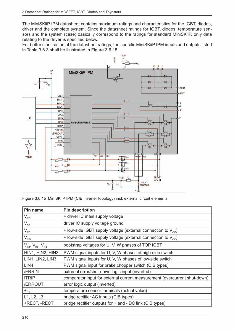
3 Datasheet Ratings for MOSFET, IGBT, Diodes and Thyristors
210
The MiniSKiiP IPM datasheet contains maximum ratings and characteristics for the IGBT, diodes, driver and the complete system. Since the datasheet ratings for IGBT, diodes, temperature sen-sors and the system (case) basically correspond to the ratings for standard MiniSKiiP, only data relating to the driver is specifi ed below. For better clarifi cation of the datasheet ratings, the specifi c MiniSKiiP IPM inputs and outputs listed in Table 3.6.3 shall be illustrated in Figure 3.6.15.
Figure 3.6.15 MiniSKiiP IPM (CIB inverter topology) incl. external circuit elements
Pin name Pin description
V CC
+ driver IC main supply voltage
V SS
driver IC supply voltage ground
V CCL
+ low-side IGBT supply voltage (external connection to V CC
)
V SSL
+ low-side IGBT supply voltage (external connection to V CC
)
V B1
, V B2
, V B3
bootstrap voltages for U, V, W phases of TOP IGBT
HIN1, HIN2, HIN3 PWM signal inputs for U, V, W phases of high-side switch
LIN1, LIN2, LIN3 PWM signal inputs for U, V, W phases of low-side switch
LIN4 PWM signal input for brake chopper switch (CIB types)
/ERRIN external error/shut-down logic input (inverted)
ITRIP comparator input for external current measurement (overcurrent shut-down)
/ERROUT error logic output (inverted)
+T, -T temperature sensor terminals (actual value)
L1, L2, L3 bridge rectifi er AC inputs (CIB types)
+RECT, -RECT bridge rectifi er outputs for + and - DC link (CIB types)

3 Datasheet Ratings for MOSFET, IGBT, Diodes and Thyristors
211
Pin name Pin description
P +DC-link input
NU, NV, NW - DC link input for U, V, W phases
U, V, W U, V, W phase AC-outputs
+B, B, -B brake chopper terminals +DC, collector, -DC (CIB types)
Table 3.6.3 Pins of a MiniSKiiP IPM inverter
For control and driver power transmission to the TOP IGBT of the U, V and W phases, level shifter / bootstrap circuits are used. Figure 3.6.16 shows the basic bootstrap circuit for the TOP IGBT of one phase, illustrating the function of the terminals V
B1 , V
B2 and V
B3 .
CBSxDBSxRBSx
RSHUNT
HV-SOI
DRIVER IC
+DC
-DC/N
+15V
VRx VDx
VSx
VBx
LOW
Side
HIGH
Side
I BS
x
VS
HU
NT
VC
C
VCx
VCC
U, V or W
VC
E-O
N
ZDBSx
VF
-CA
L
Figure 3.6.16 Basic bootstrap circuit of a TOP IGBT of one phase
Further details can be found in "Technical Explanations MiniSKiiP IPM" at www.semikron.com.
3.6.2.1 Maximum ratings of the MiniSKiiP IPM driver
Figure 3.6.17 Datasheet excerpt: maximum ratings of the MiniSKiiP IPM driver
All maximum ratings indicated in the datasheet refer to a heatsink temperature of 25°C.
Driver supply voltage V CC
Absolute maximum supply voltage applied between V CC
and V SS
or V CCL
and V SSL
High-side "fl oating" supply voltage V Bx
Absolute maximum voltage applied between the following terminals: V B1
-U, V B2
-V, V B3
-W
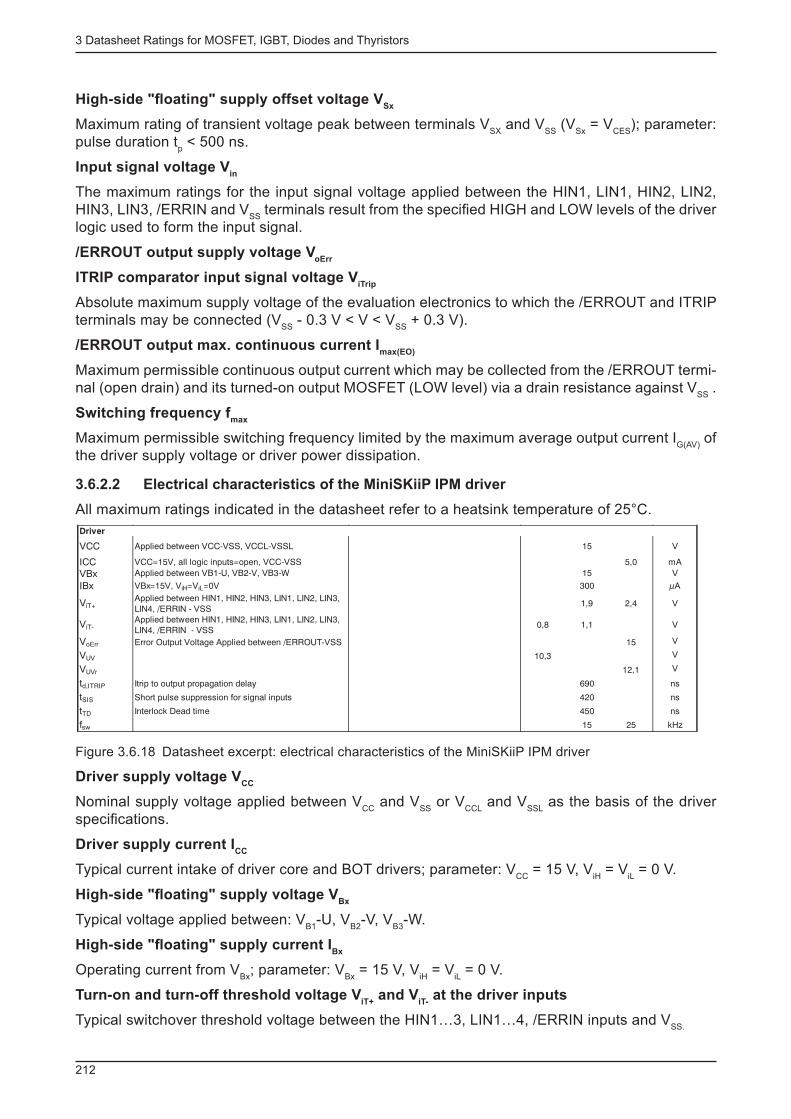
3 Datasheet Ratings for MOSFET, IGBT, Diodes and Thyristors
212
High-side "fl oating" supply offset voltage V Sx
Maximum rating of transient voltage peak between terminals V SX
and V SS
(V Sx
= V CES
); parameter: pulse duration t
p < 500 ns.
Input signal voltage V in
The maximum ratings for the input signal voltage applied between the HIN1, LIN1, HIN2, LIN2, HIN3, LIN3, /ERRIN and V
SS terminals result from the specifi ed HIGH and LOW levels of the driver
logic used to form the input signal.
/ERROUT output supply voltage V oErr
ITRIP comparator input signal voltage V iTrip
Absolute maximum supply voltage of the evaluation electronics to which the /ERROUT and ITRIP terminals may be connected (V
SS - 0.3 V < V < V
SS + 0.3 V).
/ERROUT output max. continuous current I max(EO)
Maximum permissible continuous output current which may be collected from the /ERROUT termi-nal (open drain) and its turned-on output MOSFET (LOW level) via a drain resistance against V
SS .
Switching frequency f max
Maximum permissible switching frequency limited by the maximum average output current I G(AV)
of the driver supply voltage or driver power dissipation.
3.6.2.2 Electrical characteristics of the MiniSKiiP IPM driver
All maximum ratings indicated in the datasheet refer to a heatsink temperature of 25°C.
Figure 3.6.18 Datasheet excerpt: electrical characteristics of the MiniSKiiP IPM driver
Driver supply voltage V CC
Nominal supply voltage applied between V CC
and V SS
or V CCL
and V SSL
as the basis of the driver specifi cations.
Driver supply current I CC
Typical current intake of driver core and BOT drivers; parameter: V CC
= 15 V, V iH
= V iL = 0 V.
High-side "fl oating" supply voltage V Bx
Typical voltage applied between: V B1
-U, V B2
-V, V B3
-W.
High-side "fl oating" supply current I Bx
Operating current from V Bx
; parameter: V Bx
= 15 V, V iH
= V iL = 0 V.
Turn-on and turn-off threshold voltage V iT+
and V iT-
at the driver inputs
Typical switchover threshold voltage between the HIN1…3, LIN1…4, /ERRIN inputs and V SS .

3 Datasheet Ratings for MOSFET, IGBT, Diodes and Thyristors
213
/ERROUT output supply voltage V oErr
Typical output voltage of the error memory (between /ERROUT and V SS
) under nominal conditions; the /ERROUT will be set to LOW due to the errors "undervoltage" or "external error (/ERRIN = LOW)". Subsequent error memory reset is only possible when triggering errors no longer exist, the /ERRIN input has been on HIGH level for at least 9.5 µs, and the HIN1… 3 and LIN1…3 inputs have been set to LOW level likewise for a minimum of 9.5 μs.
Undervoltage threshold V UV
If the driver supply voltage V CC
falls below the limit for V UV
, the integrated undervoltage protection will trigger an error signal, blocking the IGBT and setting the /ERROUT output to LOW.
Undervoltage threshold reset V UVr
If the error memory has been set as a consequence of undervoltage, reset will only be possible once the driver supply voltage V
CC has exceeded V
UVr .
Overcurrent turn-off delay time t d,ITRIP
Delay time between the moment when the overcurrent trip level I TRIP
is reached and the TOP and BOT IGBT is turned off; parameters: V
C = 15 V, V
iH = 3.3 V, V
iL = 0 V, V
ITRIP = 1 V.
Minimum input pulse width (short-pulse suppression) t SPS
Minimum pulse width of input and output signals. Shorter pulses are suppressed.
IGBT interlock dead time t TD
The MiniSKiiP IPM generates an interlock dead time of 450 ns.If both control inputs (HIN/LIN) of a channel are on HIGH level, the TOP and BOT-IGBT will be turned off. This event will not be indicated as an error.

3 Datasheet Ratings for MOSFET, IGBT, Diodes and Thyristors
214
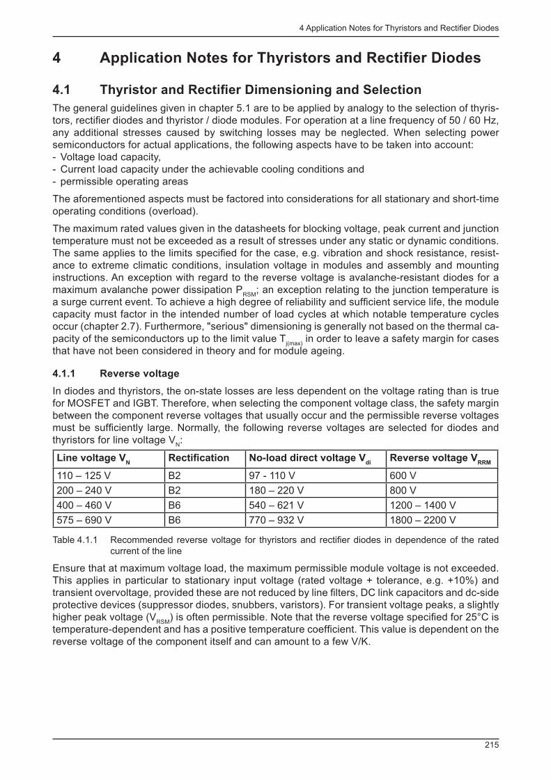
4 Application Notes for Thyristors and Rectifi er Diodes
215
4 Application Notes for Thyristors and Rectifi er Diodes
4.1 Thyristor and Rectifi er Dimensioning and Selection
The general guidelines given in chapter 5.1 are to be applied by analogy to the selection of thyris-tors, rectifi er diodes and thyristor / diode modules. For operation at a line frequency of 50 / 60 Hz, any additional stresses caused by switching losses may be neglected. When selecting power semiconductors for actual applications, the following aspects have to be taken into account: - Voltage load capacity, - Current load capacity under the achievable cooling conditions and - permissible operating areas
The aforementioned aspects must be factored into considerations for all stationary and short-time operating conditions (overload).
The maximum rated values given in the datasheets for blocking voltage, peak current and junction temperature must not be exceeded as a result of stresses under any static or dynamic conditions. The same applies to the limits specifi ed for the case, e.g. vibration and shock resistance, resist-ance to extreme climatic conditions, insulation voltage in modules and assembly and mounting instructions. An exception with regard to the reverse voltage is avalanche-resistant diodes for a maximum avalanche power dissipation P
RSM ; an exception relating to the junction temperature is
a surge current event. To achieve a high degree of reliability and suffi cient service life, the module capacity must factor in the intended number of load cycles at which notable temperature cycles occur (chapter 2.7). Furthermore, "serious" dimensioning is generally not based on the thermal ca-pacity of the semiconductors up to the limit value T
j(max) in order to leave a safety margin for cases
that have not been considered in theory and for module ageing.
4.1.1 Reverse voltage
In diodes and thyristors, the on-state losses are less dependent on the voltage rating than is true for MOSFET and IGBT. Therefore, when selecting the component voltage class, the safety margin between the component reverse voltages that usually occur and the permissible reverse voltages must be suffi ciently large. Normally, the following reverse voltages are selected for diodes and thyristors for line voltage V
N :
Line voltage V N
Rectifi cation No-load direct voltage V di
Reverse voltage V RRM
110 – 125 V B2 97 - 110 V 600 V
200 – 240 V B2 180 – 220 V 800 V
400 – 460 V B6 540 – 621 V 1200 – 1400 V
575 – 690 V B6 770 – 932 V 1800 – 2200 V
Table 4.1.1 Recommended reverse voltage for thyristors and rectifi er diodes in dependence of the rated current of the line
Ensure that at maximum voltage load, the maximum permissible module voltage is not exceeded. This applies in particular to stationary input voltage (rated voltage + tolerance, e.g. +10%) and transient overvoltage, provided these are not reduced by line fi lters, DC link capacitors and dc-side protective devices (suppressor diodes, snubbers, varistors). For transient voltage peaks, a slightly higher peak voltage (V
RSM ) is often permissible. Note that the reverse voltage specifi ed for 25°C is
temperature-dependent and has a positive temperature coeffi cient. This value is dependent on the reverse voltage of the component itself and can amount to a few V/K.

4 Application Notes for Thyristors and Rectifi er Diodes
216
4.1.2 Rectifi er diodes
4.1.2.1 Thermal load in continuous duty
The forward current load in continuous duty is related to the product of the mean power dissipation P
FAV and total thermal resistance R
th(j-a) . This product must not exceed the difference between the
ambient temperature T a and the maximum permissible virtual junction temperature T
j :
aj)aj(thFAV TTRP -£× -
The following general formula is used to calculate the power dissipation:
2
FRMSjFFAVj0FFAV I)T(rI)T(VP ×+×=
For the typical diode current waveforms (180° sinusoidal, 120° rectangular), the current (wave)form factor can easily be calculated as follows:
FAV
FRMSI
I
IF =
Thus, P FAV
still depends on one unknown only; in most cases, representation with I FAV
is selected:
2
FAV
2
IjFFAVj0FFAV IF)T(rI)T(VP ××+×=
These formulae form the basis of almost every component design software tool (see chapter 4.1.6). Nonetheless, datasheets contain numerous graphs and characteristics to help the user with product selection. Descriptions on how to use these characteristics are given below.
Low-power rectifi er diodes
Datasheets often contain diagrams for these components that show the permissible I FAV
as a per-centage of the rated on-state current as a function of the ambient temperature T
a (Figure 4.1.1).
0,0%
20,0%
40,0%
60,0%
80,0%
100,0%
120,0%
0 50 100 150 200Ta [°C]
IFAV
Figure 4.1.1 Permissible mean on-state current I FAV
(as percentage of I FAV
at T a = 50°C) as a function of
the ambient temperature T a under the cooling conditions specifi ed in the datasheet.
Power diodes
Here, diagrams such as that shown in Figure 4.1.2 are used to determine the permissible mean forward current for certain cooling conditions and vice-versa to determine the necessary cooling conditions for a given current. The curves on the left of Figure 4.1.2 end at the current densities that correspond to the max. permissible effective forward current l
FRMS , which limits the permissible
on-state load even under optimum cooling conditions.
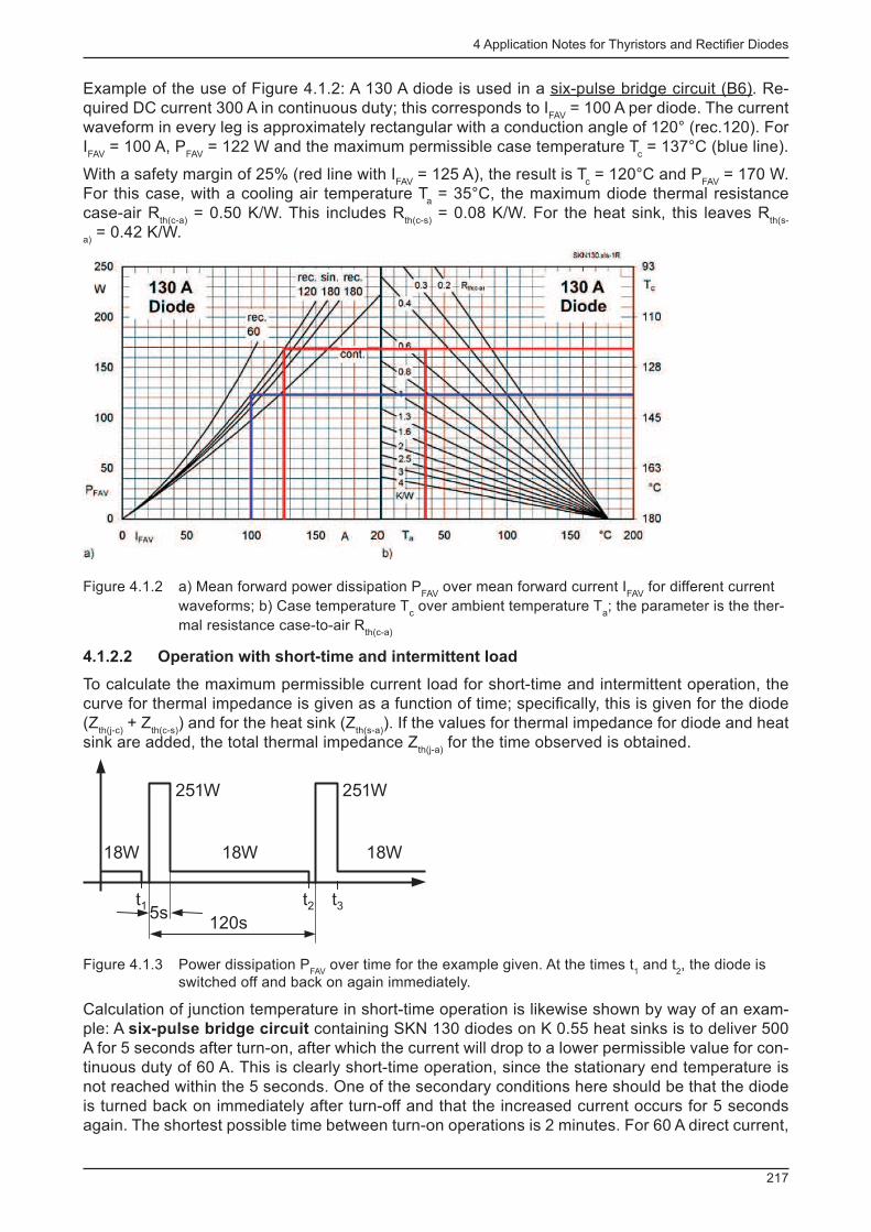
4 Application Notes for Thyristors and Rectifi er Diodes
217
Example of the use of Figure 4.1.2: A 130 A diode is used in a six-pulse bridge circuit (B6). Re-quired DC current 300 A in continuous duty; this corresponds to I
FAV = 100 A per diode. The current
waveform in every leg is approximately rectangular with a conduction angle of 120° (rec.120). For I FAV
= 100 A, P FAV
= 122 W and the maximum permissible case temperature T c = 137°C (blue line).
With a safety margin of 25% (red line with I FAV
= 125 A), the result is T c = 120°C and P
FAV = 170 W.
For this case, with a cooling air temperature T a = 35°C, the maximum diode thermal resistance
case-air R th(c-a)
= 0.50 K/W. This includes R th(c-s)
= 0.08 K/W. For the heat sink, this leaves R th(s-
a) = 0.42 K/W.
Figure 4.1.2 a) Mean forward power dissipation P FAV
over mean forward current I FAV
for different current waveforms; b) Case temperature T
c over ambient temperature T
a ; the parameter is the ther-
mal resistance case-to-air R th(c-a)
4.1.2.2 Operation with short-time and intermittent load
To calculate the maximum permissible current load for short-time and intermittent operation, the curve for thermal impedance is given as a function of time; specifi cally, this is given for the diode (Z
th(j-c) + Z
th(c-s) ) and for the heat sink (Z
th(s-a) ). If the values for thermal impedance for diode and heat
sink are added, the total thermal impedance Z th(j-a)
for the time observed is obtained.
t1 t2 t3120s
5s
18W 18W 18W
251W 251W
Figure 4.1.3 Power dissipation P FAV
over time for the example given. At the times t 1 and t
2 , the diode is
switched off and back on again immediately.
Calculation of junction temperature in short-time operation is likewise shown by way of an exam-ple: A six-pulse bridge circuit containing SKN 130 diodes on K 0.55 heat sinks is to deliver 500 A for 5 seconds after turn-on, after which the current will drop to a lower permissible value for con-tinuous duty of 60 A. This is clearly short-time operation, since the stationary end temperature is not reached within the 5 seconds. One of the secondary conditions here should be that the diode is turned back on immediately after turn-off and that the increased current occurs for 5 seconds again. The shortest possible time between turn-on operations is 2 minutes. For 60 A direct current,
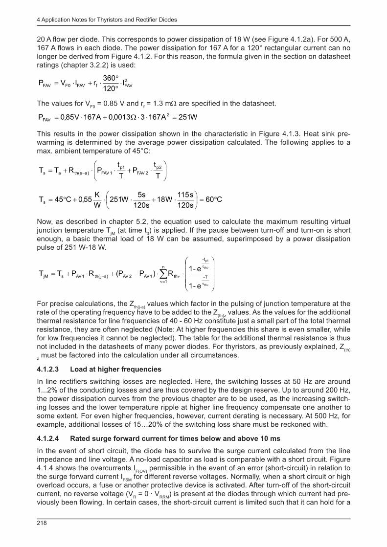
4 Application Notes for Thyristors and Rectifi er Diodes
218
20 A fl ow per diode. This corresponds to power dissipation of 18 W (see Figure 4.1.2a). For 500 A, 167 A fl ows in each diode. The power dissipation for 167 A for a 120° rectangular current can no longer be derived from Figure 4.1.2. For this reason, the formula given in the section on datasheet ratings (chapter 3.2.2) is used:
2
FAVfFAV0FFAV I120
360rIVP ×
°°
×+×=
The values for V F0
= 0.85 V and r f = 1.3 mΩ are specifi ed in the datasheet.
W251A16730013,0A167V85,0P 2
FAV =××W+×=
This results in the power dissipation shown in the characteristic in Figure 4.1.3. Heat sink pre-warming is determined by the average power dissipation calculated. The following applies to a max. ambient temperature of 45°C:
÷÷ø
öççè
æ×+××+= -
T
tP
T
tPRTT
2p
2FAV
1p
1FAV)as(thas
C60
s120
s115W18
s120
s5W251
W
K55,0C45Ts °=÷
ø
öçè
æ×+××+°=
Now, as described in chapter 5.2, the equation used to calculate the maximum resulting virtual junction temperature T
jM (at time t
3 ) is applied. If the pause between turn-off and turn-on is short
enough, a basic thermal load of 18 W can be assumed, superimposed by a power dissipation pulse of 251 W-18 W.
å=n t
t
n-
÷÷÷÷
ø
ö
çççç
è
æ
××-+×+=n
nn
1T-
-t
th1AV2AV)sj(th1AVsjM
th
th
p1
e-1
e-1R)PP(RPTT
For precise calculations, the Z th(j-a)
values which factor in the pulsing of junction temperature at the rate of the operating frequency have to be added to the Z
(th)z values. As the values for the additional
thermal resistance for line frequencies of 40 - 60 Hz constitute just a small part of the total thermal resistance, they are often neglected (Note: At higher frequencies this share is even smaller, while for low frequencies it cannot be neglected). The table for the additional thermal resistance is thus not included in the datasheets of many power diodes. For thyristors, as previously explained, Z
(th)
z must be factored into the calculation under all circumstances.
4.1.2.3 Load at higher frequencies
In line rectifi ers switching losses are neglected. Here, the switching losses at 50 Hz are around 1...2% of the conducting losses and are thus covered by the design reserve. Up to around 200 Hz, the power dissipation curves from the previous chapter are to be used, as the increasing switch-ing losses and the lower temperature ripple at higher line frequency compensate one another to some extent. For even higher frequencies, however, current derating is necessary. At 500 Hz, for example, additional losses of 15…20% of the switching loss share must be reckoned with.
4.1.2.4 Rated surge forward current for times below and above 10 ms
In the event of short circuit, the diode has to survive the surge current calculated from the line impedance and line voltage. A no-load capacitor as load is comparable with a short circuit. Figure 4.1.4 shows the overcurrents I
F(OV) permissible in the event of an error (short-circuit) in relation to
the surge forward current I FSM
for different reverse voltages. Normally, when a short circuit or high overload occurs, a fuse or another protective device is activated. After turn-off of the short-circuit current, no reverse voltage (V
R = 0 · V
RRM ) is present at the diodes through which current had pre-
viously been fl owing. In certain cases, the short-circuit current is limited such that it can hold for a
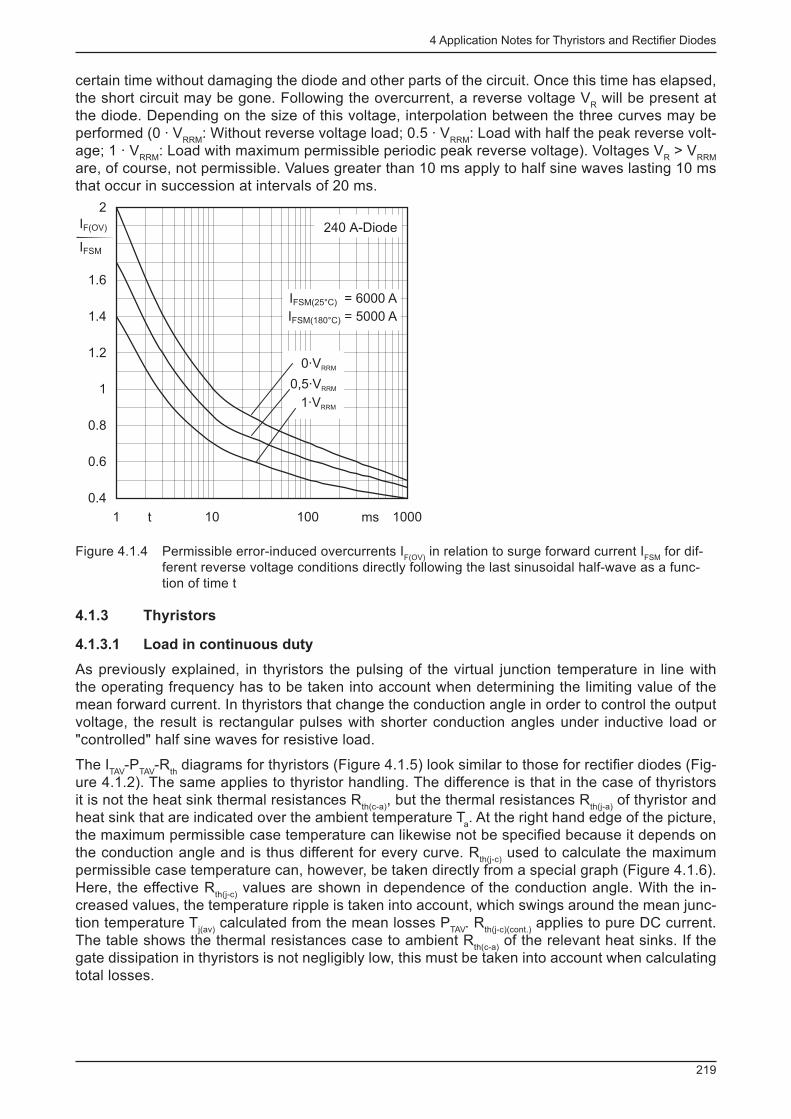
4 Application Notes for Thyristors and Rectifi er Diodes
219
certain time without damaging the diode and other parts of the circuit. Once this time has elapsed, the short circuit may be gone. Following the overcurrent, a reverse voltage V
R will be present at
the diode. Depending on the size of this voltage, interpolation between the three curves may be performed (0 · V
RRM : Without reverse voltage load; 0.5 · V
RRM : Load with half the peak reverse volt-
age; 1 · V RRM
: Load with maximum permissible periodic peak reverse voltage). Voltages V R > V
RRM
are, of course, not permissible. Values greater than 10 ms apply to half sine waves lasting 10 ms that occur in succession at intervals of 20 ms.
0.4
0.6
0.8
1
1.2
1.4
1.6
1,8
2
1 10 100 1000mst
IF(OV)
IFSM
I = 6000 AFSM(25°C)
I = 5000 AFSM(180°C)
240 A-Diode
0·VRRM
0,5·VRRM
1·VRRM
Figure 4.1.4 Permissible error-induced overcurrents I F(OV)
in relation to surge forward current I FSM
for dif-ferent reverse voltage conditions directly following the last sinusoidal half-wave as a func-tion of time t
4.1.3 Thyristors
4.1.3.1 Load in continuous duty
As previously explained, in thyristors the pulsing of the virtual junction temperature in line with the operating frequency has to be taken into account when determining the limiting value of the mean forward current. In thyristors that change the conduction angle in order to control the output voltage, the result is rectangular pulses with shorter conduction angles under inductive load or "controlled" half sine waves for resistive load.
The I TAV
-P TAV
-R th diagrams for thyristors (Figure 4.1.5) look similar to those for rectifi er diodes (Fig-
ure 4.1.2). The same applies to thyristor handling. The difference is that in the case of thyristors it is not the heat sink thermal resistances R
th(c-a) , but the thermal resistances R
th(j-a) of thyristor and
heat sink that are indicated over the ambient temperature T a . At the right hand edge of the picture,
the maximum permissible case temperature can likewise not be specifi ed because it depends on the conduction angle and is thus different for every curve. R
th(j-c) used to calculate the maximum
permissible case temperature can, however, be taken directly from a special graph (Figure 4.1.6). Here, the effective R
th(j-c) values are shown in dependence of the conduction angle. With the in-
creased values, the temperature ripple is taken into account, which swings around the mean junc-tion temperature T
j(av) calculated from the mean losses P
TAV . R
th(j-c)(cont.) applies to pure DC current.
The table shows the thermal resistances case to ambient R th(c-a)
of the relevant heat sinks. If the gate dissipation in thyristors is not negligibly low, this must be taken into account when calculating total losses.
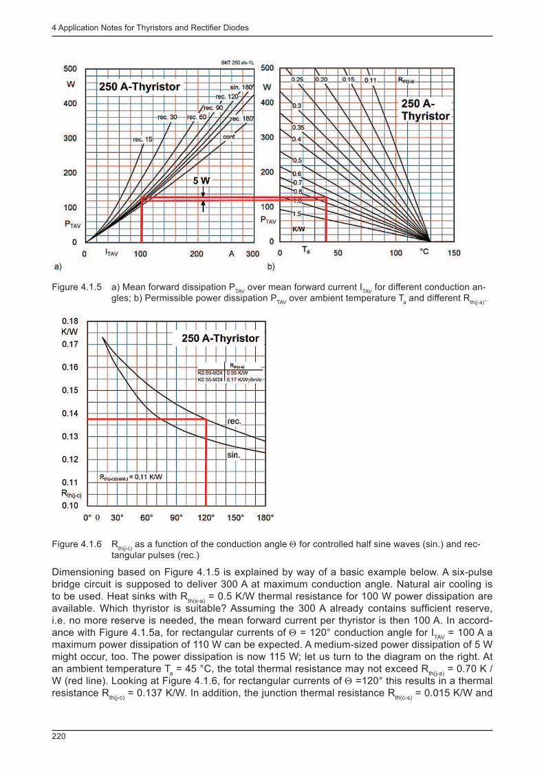
4 Application Notes for Thyristors and Rectifi er Diodes
220
Figure 4.1.5 a) Mean forward dissipation P TAV
over mean forward current I TAV
for different conduction an-gles; b) Permissible power dissipation P
TAV over ambient temperature T
a and different R
th(j-a) .
Figure 4.1.6 R th(j-c)
as a function of the conduction angle Θ for controlled half sine waves (sin.) and rec-tangular pulses (rec.)
Dimensioning based on Figure 4.1.5 is explained by way of a basic example below. A six-pulse bridge circuit is supposed to deliver 300 A at maximum conduction angle. Natural air cooling is to be used. Heat sinks with R
th(s-a) = 0.5 K/W thermal resistance for 100 W power dissipation are
available. Which thyristor is suitable? Assuming the 300 A already contains suffi cient reserve, i.e. no more reserve is needed, the mean forward current per thyristor is then 100 A. In accord-ance with Figure 4.1.5a, for rectangular currents of Θ = 120° conduction angle for I
TAV = 100 A a
maximum power dissipation of 110 W can be expected. A medium-sized power dissipation of 5 W might occur, too. The power dissipation is now 115 W; let us turn to the diagram on the right. At an ambient temperature T
a = 45 °C, the total thermal resistance may not exceed R
th(j-a) = 0.70 K /
W (red line). Looking at Figure 4.1.6, for rectangular currents of Θ =120° this results in a thermal resistance R
th(j-c) = 0.137 K/W. In addition, the junction thermal resistance R
th(c-s) = 0.015 K/W and
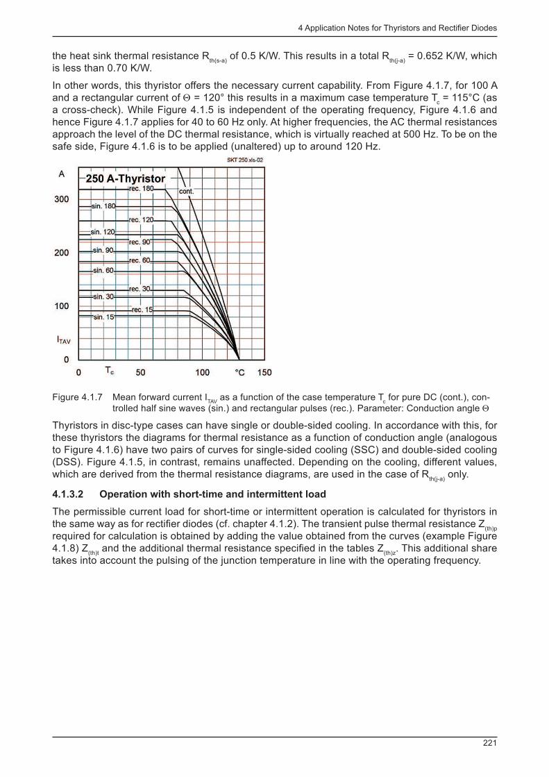
4 Application Notes for Thyristors and Rectifi er Diodes
221
the heat sink thermal resistance R th(s-a)
of 0.5 K/W. This results in a total R th(j-a)
= 0.652 K/W, which is less than 0.70 K/W.
In other words, this thyristor offers the necessary current capability. From Figure 4.1.7, for 100 A and a rectangular current of Θ = 120° this results in a maximum case temperature T
c = 115°C (as
a cross-check). While Figure 4.1.5 is independent of the operating frequency, Figure 4.1.6 and hence Figure 4.1.7 applies for 40 to 60 Hz only. At higher frequencies, the AC thermal resistances approach the level of the DC thermal resistance, which is virtually reached at 500 Hz. To be on the safe side, Figure 4.1.6 is to be applied (unaltered) up to around 120 Hz.
Figure 4.1.7 Mean forward current I TAV
as a function of the case temperature T c for pure DC (cont.), con-
trolled half sine waves (sin.) and rectangular pulses (rec.). Parameter: Conduction angle Θ
Thyristors in disc-type cases can have single or double-sided cooling. In accordance with this, for these thyristors the diagrams for thermal resistance as a function of conduction angle (analogous to Figure 4.1.6) have two pairs of curves for single-sided cooling (SSC) and double-sided cooling (DSS). Figure 4.1.5, in contrast, remains unaffected. Depending on the cooling, different values, which are derived from the thermal resistance diagrams, are used in the case of R
th(j-a) only.
4.1.3.2 Operation with short-time and intermittent load
The permissible current load for short-time or intermittent operation is calculated for thyristors in the same way as for rectifi er diodes (cf. chapter 4.1.2). The transient pulse thermal resistance Z
(th)p
required for calculation is obtained by adding the value obtained from the curves (example Figure 4.1.8) Z
(th)t and the additional thermal resistance specifi ed in the tables Z
(th)z . This additional share
takes into account the pulsing of the junction temperature in line with the operating frequency.

4 Application Notes for Thyristors and Rectifi er Diodes
222
Figure 4.1.8 Z th of a thyristor for SSC and DSC
4.1.3.3 Maximum surge on-state current for times below and above 10 ms
For thyristors, the same applies as for diodes (cf. chapter 4.1.2.4). In addition, it must be borne in mind that for the higher junction temperature that occurs during the surge on-state current load, thyristor controllability is lost temporarily. Thus, the thyristor behaves likes a rectifi er diode, i.e. under voltage load it goes immediately into forward on-state.
4.1.3.4 Critical rate of rise of current and voltage
In addition to pure thermal rating, for thyristors care must be taken that the critical rate of rise of current (di/dt)
cr and the critical rate of rise of voltage (dv/dt)
cr are adhered to. The RC element that
is normally connected in parallel to the thyristor, already induces a considerable di/dt. This is why the rate of rise of current caused by the rest of the circuit should lie far below the critical value. In rectifi ers, even relatively small RC elements can result in a reduction of the voltage rate of rise to very low values that the thyristors can easily cope with. The same applies to a.c. power converters and circuit breakers. In inverters and especially in 4-quadrant converters, by way of contrast, the rapid drop in voltage when the thyristor is triggered causes steep voltage peeks at the thyristors of the other branches in forward direction. These voltage peaks are barely attenuated by the RC circuit since the only series resistance is the switching inductance. This is why, for such applica-tions, thyristors with a high critical voltage rate of rise (1000 V/µs) are used.
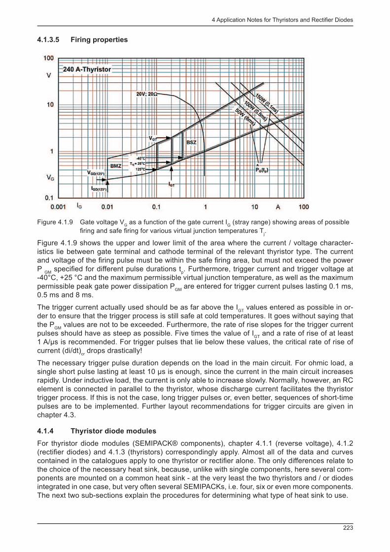
4 Application Notes for Thyristors and Rectifi er Diodes
223
4.1.3.5 Firing properties
Figure 4.1.9 Gate voltage V G as a function of the gate current I
G (stray range) showing areas of possible
fi ring and safe fi ring for various virtual junction temperatures T j .
Figure 4.1.9 shows the upper and lower limit of the area where the current / voltage character-istics lie between gate terminal and cathode terminal of the relevant thyristor type. The current and voltage of the fi ring pulse must be within the safe fi ring area, but must not exceed the power P
GM specifi ed for different pulse durations t
p . Furthermore, trigger current and trigger voltage at
-40°C, +25 °C and the maximum permissible virtual junction temperature, as well as the maximum permissible peak gate power dissipation P
GM are entered for trigger current pulses lasting 0.1 ms,
0.5 ms and 8 ms.
The trigger current actually used should be as far above the I GT
values entered as possible in or-der to ensure that the trigger process is still safe at cold temperatures. It goes without saying that the P
GM values are not to be exceeded. Furthermore, the rate of rise slopes for the trigger current
pulses should have as steep as possible. Five times the value of I GT
and a rate of rise of at least 1 A/µs is recommended. For trigger pulses that lie below these values, the critical rate of rise of current (di/dt)
cr drops drastically!
The necessary trigger pulse duration depends on the load in the main circuit. For ohmic load, a single short pulse lasting at least 10 µs is enough, since the current in the main circuit increases rapidly. Under inductive load, the current is only able to increase slowly. Normally, however, an RC element is connected in parallel to the thyristor, whose discharge current facilitates the thyristor trigger process. If this is not the case, long trigger pulses or, even better, sequences of short-time pulses are to be implemented. Further layout recommendations for trigger circuits are given in chapter 4.3.
4.1.4 Thyristor diode modules
For thyristor diode modules (SEMIPACK® components), chapter 4.1.1 (reverse voltage), 4.1.2 (rectifi er diodes) and 4.1.3 (thyristors) correspondingly apply. Almost all of the data and curves contained in the catalogues apply to one thyristor or rectifi er alone. The only differences relate to the choice of the necessary heat sink, because, unlike with single components, here several com-ponents are mounted on a common heat sink - at the very least the two thyristors and / or diodes integrated in one case, but very often several SEMIPACKs, i.e. four, six or even more components. The next two sub-sections explain the procedures for determining what type of heat sink to use.
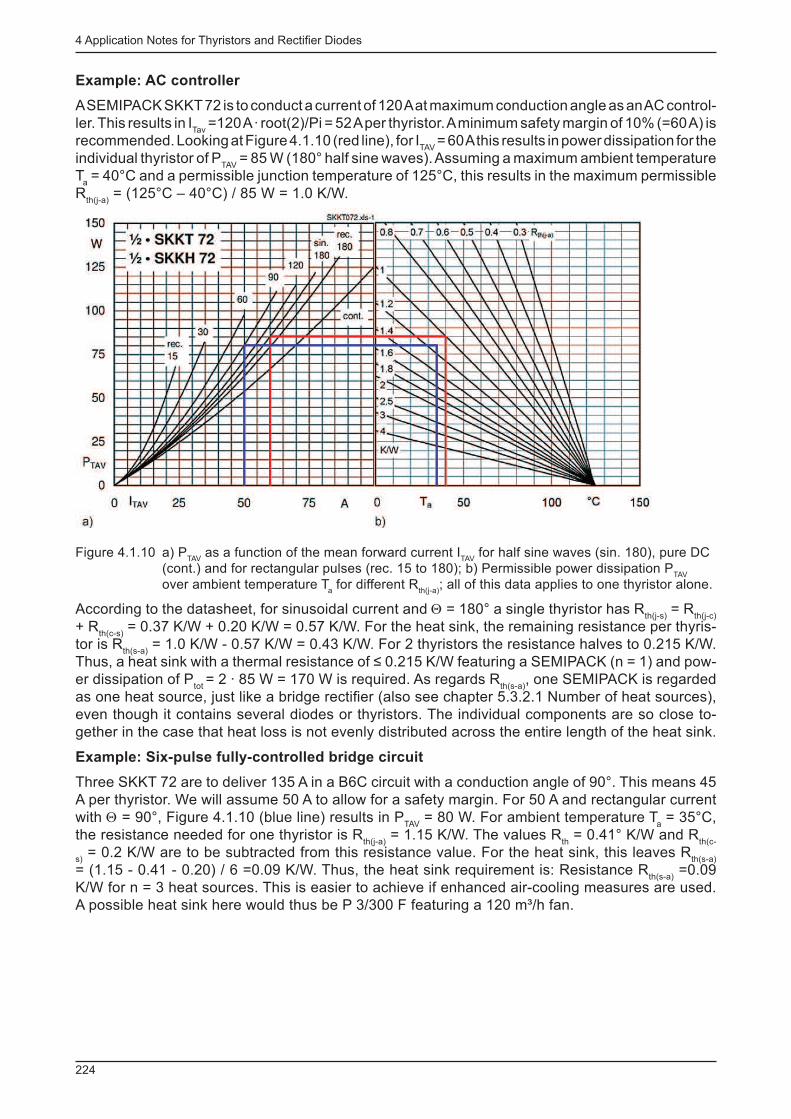
4 Application Notes for Thyristors and Rectifi er Diodes
224
Example: AC controller
A SEMIPACK SKKT 72 is to conduct a current of 120 A at maximum conduction angle as an AC control-ler. This results in I
Tav =120 A · root(2)/Pi = 52 A per thyristor. A minimum safety margin of 10% (=60 A) is
recommended. Looking at Figure 4.1.10 (red line), for I TAV
= 60 A this results in power dissipation for the individual thyristor of P
TAV = 85 W (180° half sine waves). Assuming a maximum ambient temperature
T a = 40°C and a permissible junction temperature of 125°C, this results in the maximum permissible
R th(j-a)
= (125°C – 40°C) / 85 W = 1.0 K/W.
Figure 4.1.10 a) P TAV
as a function of the mean forward current I TAV
for half sine waves (sin. 180), pure DC (cont.) and for rectangular pulses (rec. 15 to 180); b) Permissible power dissipation P
TAV
over ambient temperature T a for different R
th(j-a) ; all of this data applies to one thyristor alone.
According to the datasheet, for sinusoidal current and Θ = 180° a single thyristor has R th(j-s)
= R th(j-c)
+ R
th(c-s) = 0.37 K/W + 0.20 K/W = 0.57 K/W. For the heat sink, the remaining resistance per thyris-
tor is R th(s-a)
= 1.0 K/W - 0.57 K/W = 0.43 K/W. For 2 thyristors the resistance halves to 0.215 K/W. Thus, a heat sink with a thermal resistance of ≤ 0.215 K/W featuring a SEMIPACK (n = 1) and pow-er dissipation of P
tot = 2 · 85 W = 170 W is required. As regards R
th(s-a) , one SEMIPACK is regarded
as one heat source, just like a bridge rectifi er (also see chapter 5.3.2.1 Number of heat sources), even though it contains several diodes or thyristors. The individual components are so close to-gether in the case that heat loss is not evenly distributed across the entire length of the heat sink.
Example: Six-pulse fully-controlled bridge circuit
Three SKKT 72 are to deliver 135 A in a B6C circuit with a conduction angle of 90°. This means 45 A per thyristor. We will assume 50 A to allow for a safety margin. For 50 A and rectangular current with Θ = 90°, Figure 4.1.10 (blue line) results in P
TAV = 80 W. For ambient temperature T
a = 35°C,
the resistance needed for one thyristor is R th(j-a)
= 1.15 K/W. The values R th = 0.41° K/W and R
th(c-
s) = 0.2 K/W are to be subtracted from this resistance value. For the heat sink, this leaves R
th(s-a)
= (1.15 - 0.41 - 0.20) / 6 =0.09 K/W. Thus, the heat sink requirement is: Resistance R th(s-a)
=0.09 K/W for n = 3 heat sources. This is easier to achieve if enhanced air-cooling measures are used. A possible heat sink here would thus be P 3/300 F featuring a 120 m³/h fan.
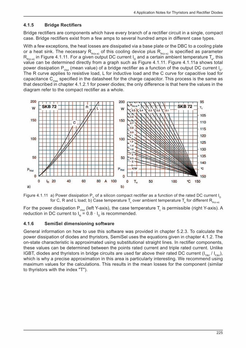
4 Application Notes for Thyristors and Rectifi er Diodes
225
4.1.5 Bridge Rectifi ers
Bridge rectifi ers are components which have every branch of a rectifi er circuit in a single, compact case. Bridge rectifi ers exist from a few amps to several hundred amps in different case types.
With a few exceptions, the heat losses are dissipated via a base plate or the DBC to a cooling plate or a heat sink. The necessary R
th(s-a) of this cooling device plus R
th(c-s) is specifi ed as parameter
R th(c-a)
in Figure 4.1.11. For a given output DC current I D and a certain ambient temperature T
a , this
value can be determined directly from a graph such as Figure 4.1.11. Figure 4.1.11a shows total power dissipation P
Vtot (mean value) of a bridge rectifi er as a function of the output DC current l
D .
The R curve applies to resistive load, L for inductive load and the C curve for capacitive load for capacitance C
max specifi ed in the datasheet for the charge capacitor. This process is the same as
that described in chapter 4.1.2.1 for power diodes; the only difference is that here the values in the diagram refer to the compact rectifi er as a whole.
Figure 4.1.11 a) Power dissipation P V of a silicon compact rectifi er as a function of the rated DC current I
D
for C, R and L load; b) Case temperature T c over ambient temperature T
a for different R
th(c-a)
For the power dissipation P Vtot
(left Y-axis), the case temperature T c is permissible (right Y-axis). A
reduction in DC current to I N = 0.8 · I
D is recommended.
4.1.6 SemiSel dimensioning software
General information on how to use this software was provided in chapter 5.2.3. To calculate the power dissipation of diodes and thyristors, SemiSel uses the equations given in chapter 4.1.2. The on-state characteristic is approximated using substitutional straight lines. In rectifi er components, these values can be determined between the points rated current and triple rated current. Unlike IGBT, diodes and thyristors in bridge circuits are used far above their rated DC current (I
TAV / I
FAV ),
which is why a precise approximation in this area is particularly interesting. We recommend using maximum values for the calculations. This results in the mean losses for the component (similar to thyristors with the index "T").
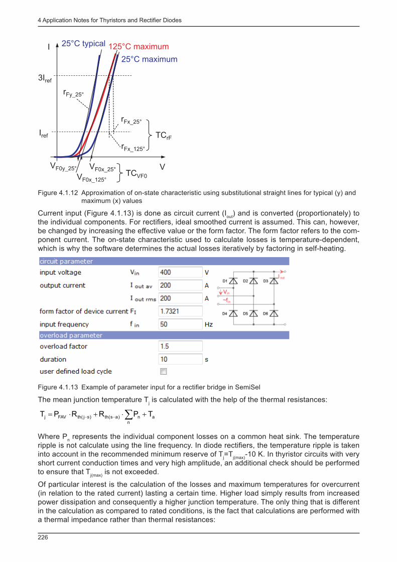
4 Application Notes for Thyristors and Rectifi er Diodes
226
3Iref
Iref
VF0y_25°
rFy_25°
25°C maximum
125°C maximum
VF0x_25°
VF0x_125°TCVF0
rFx_125°
rFx_25°
TCrF
25°C typical
V
I
Figure 4.1.12 Approximation of on-state characteristic using substitutional straight lines for typical (y) and maximum (x) values
Current input (Figure 4.1.13) is done as circuit current (I out
) and is converted (proportionately) to the individual components. For rectifi ers, ideal smoothed current is assumed. This can, however, be changed by increasing the effective value or the form factor. The form factor refers to the com-ponent current. The on-state characteristic used to calculate losses is temperature-dependent, which is why the software determines the actual losses iteratively by factoring in self-heating.
Figure 4.1.13 Example of parameter input for a rectifi er bridge in SemiSel
The mean junction temperature T j is calculated with the help of the thermal resistances:
a
n
n)as(th)sj(thFAVj TPRRPT +×+×= å--
Where P n represents the individual component losses on a common heat sink. The temperature
ripple is not calculate using the line frequency. In diode rectifi ers, the temperature ripple is taken into account in the recommended minimum reserve of T
j =T
j(max) -10 K. In thyristor circuits with very
short current conduction times and very high amplitude, an additional check should be performed to ensure that T
j(max) is not exceeded.
Of particular interest is the calculation of the losses and maximum temperatures for overcurrent (in relation to the rated current) lasting a certain time. Higher load simply results from increased power dissipation and consequently a higher junction temperature. The only thing that is different in the calculation as compared to rated conditions, is the fact that calculations are performed with a thermal impedance rather than thermal resistances:
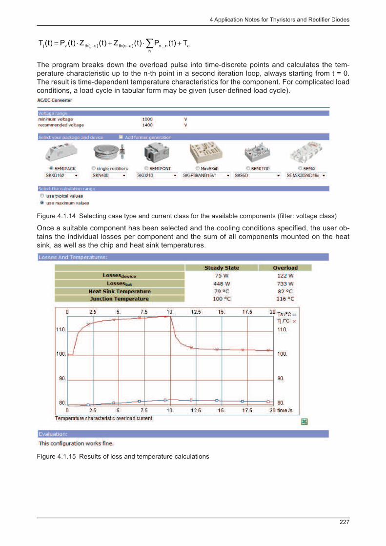
4 Application Notes for Thyristors and Rectifi er Diodes
227
a
n
n_v)as(th)sj(thvj T)t(P)t(Z)t(Z)t(P)t(T +×+×= å--
The program breaks down the overload pulse into time-discrete points and calculates the tem-perature characteristic up to the n-th point in a second iteration loop, always starting from t = 0. The result is time-dependent temperature characteristics for the component. For complicated load conditions, a load cycle in tabular form may be given (user-defi ned load cycle).
Figure 4.1.14 Selecting case type and current class for the available components (fi lter: voltage class)
Once a suitable component has been selected and the cooling conditions specifi ed, the user ob-tains the individual losses per component and the sum of all components mounted on the heat sink, as well as the chip and heat sink temperatures.
Figure 4.1.15 Results of loss and temperature calculations
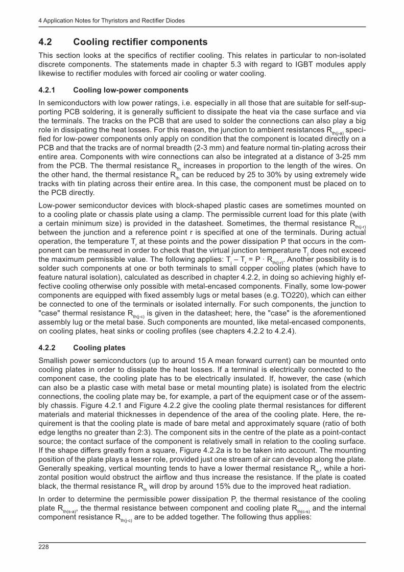
4 Application Notes for Thyristors and Rectifi er Diodes
228
4.2 Cooling rectifi er components
This section looks at the specifi cs of rectifi er cooling. This relates in particular to non-isolated discrete components. The statements made in chapter 5.3 with regard to IGBT modules apply likewise to rectifi er modules with forced air cooling or water cooling.
4.2.1 Cooling low-power components
In semiconductors with low power ratings, i.e. especially in all those that are suitable for self-sup-porting PCB soldering, it is generally suffi cient to dissipate the heat via the case surface and via the terminals. The tracks on the PCB that are used to solder the connections can also play a big role in dissipating the heat losses. For this reason, the junction to ambient resistances R
th(j-a) speci-
fi ed for low-power components only apply on condition that the component is located directly on a PCB and that the tracks are of normal breadth (2-3 mm) and feature normal tin-plating across their entire area. Components with wire connections can also be integrated at a distance of 3-25 mm from the PCB. The thermal resistance R
th increases in proportion to the length of the wires. On
the other hand, the thermal resistance R th can be reduced by 25 to 30% by using extremely wide
tracks with tin plating across their entire area. In this case, the component must be placed on to the PCB directly.
Low-power semiconductor devices with block-shaped plastic cases are sometimes mounted on to a cooling plate or chassis plate using a clamp. The permissible current load for this plate (with a certain minimum size) is provided in the datasheet. Sometimes, the thermal resistance R
th(j-r)
between the junction and a reference point r is specifi ed at one of the terminals. During actual operation, the temperature T
r at these points and the power dissipation P that occurs in the com-
ponent can be measured in order to check that the virtual junction temperature T j does not exceed
the maximum permissible value. The following applies: T j – T
r = P · R
th(j-r) . Another possibility is to
solder such components at one or both terminals to small copper cooling plates (which have to feature natural isolation), calculated as described in chapter 4.2.2, in doing so achieving highly ef-fective cooling otherwise only possible with metal-encased components. Finally, some low-power components are equipped with fi xed assembly lugs or metal bases (e.g. TO220), which can either be connected to one of the terminals or isolated internally. For such components, the junction to "case" thermal resistance R
th(j-c) is given in the datasheet; here, the "case" is the aforementioned
assembly lug or the metal base. Such components are mounted, like metal-encased components, on cooling plates, heat sinks or cooling profi les (see chapters 4.2.2 to 4.2.4).
4.2.2 Cooling plates
Smallish power semiconductors (up to around 15 A mean forward current) can be mounted onto cooling plates in order to dissipate the heat losses. If a terminal is electrically connected to the component case, the cooling plate has to be electrically insulated. If, however, the case (which can also be a plastic case with metal base or metal mounting plate) is isolated from the electric connections, the cooling plate may be, for example, a part of the equipment case or of the assem-bly chassis. Figure 4.2.1 and Figure 4.2.2 give the cooling plate thermal resistances for different materials and material thicknesses in dependence of the area of the cooling plate. Here, the re-quirement is that the cooling plate is made of bare metal and approximately square (ratio of both edge lengths no greater than 2:3). The component sits in the centre of the plate as a point-contact source; the contact surface of the component is relatively small in relation to the cooling surface. If the shape differs greatly from a square, Figure 4.2.2a is to be taken into account. The mounting position of the plate plays a lesser role, provided just one stream of air can develop along the plate. Generally speaking, vertical mounting tends to have a lower thermal resistance R
th , while a hori-
zontal position would obstruct the airfl ow and thus increase the resistance. If the plate is coated black, the thermal resistance R
th will drop by around 15% due to the improved heat radiation.
In order to determine the permissible power dissipation P, the thermal resistance of the cooling plate R
th(s-a) , the thermal resistance between component and cooling plate R
th(c-s) and the internal
component resistance R th(j-c)
are to be added together. The following thus applies:
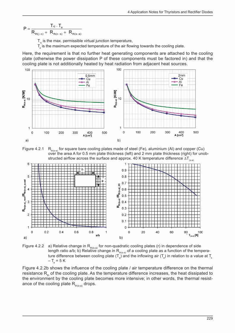
4 Application Notes for Thyristors and Rectifi er Diodes
229
)as(th)sc(th)cj(th
avj
RRR
TTP
---
-
++=
T vj is the max. permissible virtual junction temperature,
T a is the maximum expected temperature of the air fl owing towards the cooling plate.
Here, the requirement is that no further heat generating components are attached to the cooling plate (otherwise the power dissipation P of these components must be factored in) and that the cooling plate is not additionally heated by heat radiation from adjacent heat sources.
Figure 4.2.1 R th(s-a)
for square bare cooling plates made of steel (Fe), aluminium (Al) and copper (Cu) over the area A for 0.5 mm plate thickness (left) and 2 mm plate thickness (right) for unob-structed airfl ow across the surface and approx. 40 K temperature difference ∆T
(s-a)
Figure 4.2.2 a) Relative change in R th(s-a)
for non-quadratic cooling plates (r) in dependence of side length ratio a/b; b) Relative change in R
th(s-a) of a cooling plate as a function of the tempera-
ture difference between cooling plate (T s ) and the infl owing air (T
a ) in relation to a value at T
s
– T a = 5 K
Figure 4.2.2b shows the infl uence of the cooling plate / air temperature difference on the thermal resistance R
th of the cooling plate. As the temperature difference increases, the heat dissipated to
the environment by the cooling plate becomes more intensive; in other words, the thermal resist-ance of the cooling plate R
th(s-a) drops.
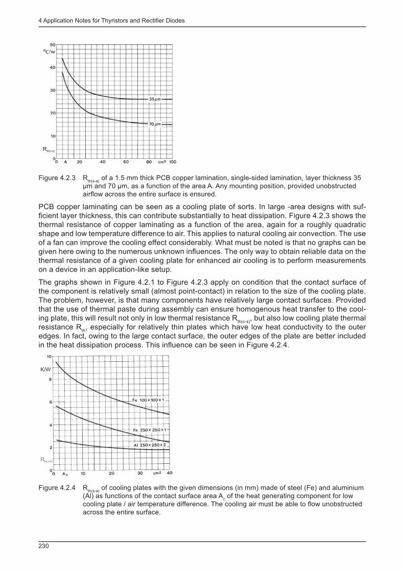
4 Application Notes for Thyristors and Rectifi er Diodes
230
Figure 4.2.3 R th(s-a)
of a 1.5 mm thick PCB copper lamination, single-sided lamination, layer thickness 35 µm and 70 µm, as a function of the area A. Any mounting position, provided unobstructed airfl ow across the entire surface is ensured.
PCB copper laminating can be seen as a cooling plate of sorts. In large -area designs with suf-fi cient layer thickness, this can contribute substantially to heat dissipation. Figure 4.2.3 shows the thermal resistance of copper laminating as a function of the area, again for a roughly quadratic shape and low temperature difference to air. This applies to natural cooling air convection. The use of a fan can improve the cooling effect considerably. What must be noted is that no graphs can be given here owing to the numerous unknown infl uences. The only way to obtain reliable data on the thermal resistance of a given cooling plate for enhanced air cooling is to perform measurements on a device in an application-like setup.
The graphs shown in Figure 4.2.1 to Figure 4.2.3 apply on condition that the contact surface of the component is relatively small (almost point-contact) in relation to the size of the cooling plate. The problem, however, is that many components have relatively large contact surfaces. Provided that the use of thermal paste during assembly can ensure homogenous heat transfer to the cool-ing plate, this will result not only in low thermal resistance R
th(c-s) , but also low cooling plate thermal
resistance R th , especially for relatively thin plates which have low heat conductivity to the outer
edges. In fact, owing to the large contact surface, the outer edges of the plate are better included in the heat dissipation process. This infl uence can be seen in Figure 4.2.4.
Figure 4.2.4 R th(s-a)
of cooling plates with the given dimensions (in mm) made of steel (Fe) and aluminium (Al) as functions of the contact surface area A
c of the heat generating component for low
cooling plate / air temperature difference. The cooling air must be able to fl ow unobstructed across the entire surface.
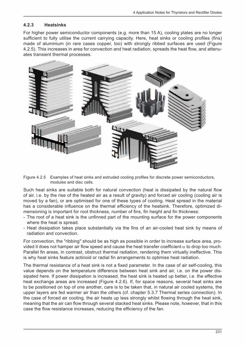
4 Application Notes for Thyristors and Rectifi er Diodes
231
4.2.3 Heatsinks
For higher power semiconductor components (e.g. more than 15 A), cooling plates are no longer suffi cient to fully utilise the current carrying capacity. Here, heat sinks or cooling profi les (fi ns) made of aluminium (in rare cases copper, too) with strongly ribbed surfaces are used (Figure 4.2.5). This increases in area for convection and heat radiation, spreads the heat fl ow, and attenu-ates transient thermal processes.
Figure 4.2.5 Examples of heat sinks and extruded cooling profi les for discrete power semiconductors, modules and disc cells.
Such heat sinks are suitable both for natural convection (heat is dissipated by the natural fl ow of air, i.e. by the rise of the heated air as a result of gravity) and forced air cooling (cooling air is moved by a fan), or are optimised for one of these types of cooling. Heat spread in the material has a considerable infl uence on the thermal effi ciency of the heatsink. Therefore, optimized di-mensioning is important for root thickness, number of fi ns, fi n height and fi n thickness: - The root of a heat sink is the unfi nned part of the mounting surface for the power components where the heat is spread.
- Heat dissipation takes place substantially via the fi ns of an air-cooled heat sink by means of radiation and convection.
For convection, the "ribbing" should be as high as possible in order to increase surface area, pro-vided it does not hamper air fl ow speed and cause the heat transfer coeffi cient α to drop too much. Parallel fi n areas, in contrast, obstruct thermal radiation, rendering them virtually ineffective. This is why heat sinks feature actinoid or radial fi n arrangements to optimise heat radiation.
The thermal resistance of a heat sink is not a fi xed parameter. In the case of air self-cooling, this value depends on the temperature difference between heat sink and air, i.e. on the power dis-sipated here. If power dissipation is increased, the heat sink is heated up better, i.e. the effective heat exchange areas are increased (Figure 4.2.6). If, for space reasons, several heat sinks are to be positioned on top of one another, care is to be taken that, in natural air cooled systems, the upper layers are fed warmer air than the others (cf. chapter 5.3.7 Thermal series connection). In the case of forced air cooling, the air heats up less strongly whilst fl owing through the heat sink, meaning that the air can fl ow through several stacked heat sinks. Please note, however, that in this case the fl ow resistance increases, reducing the effi ciency of the fan.
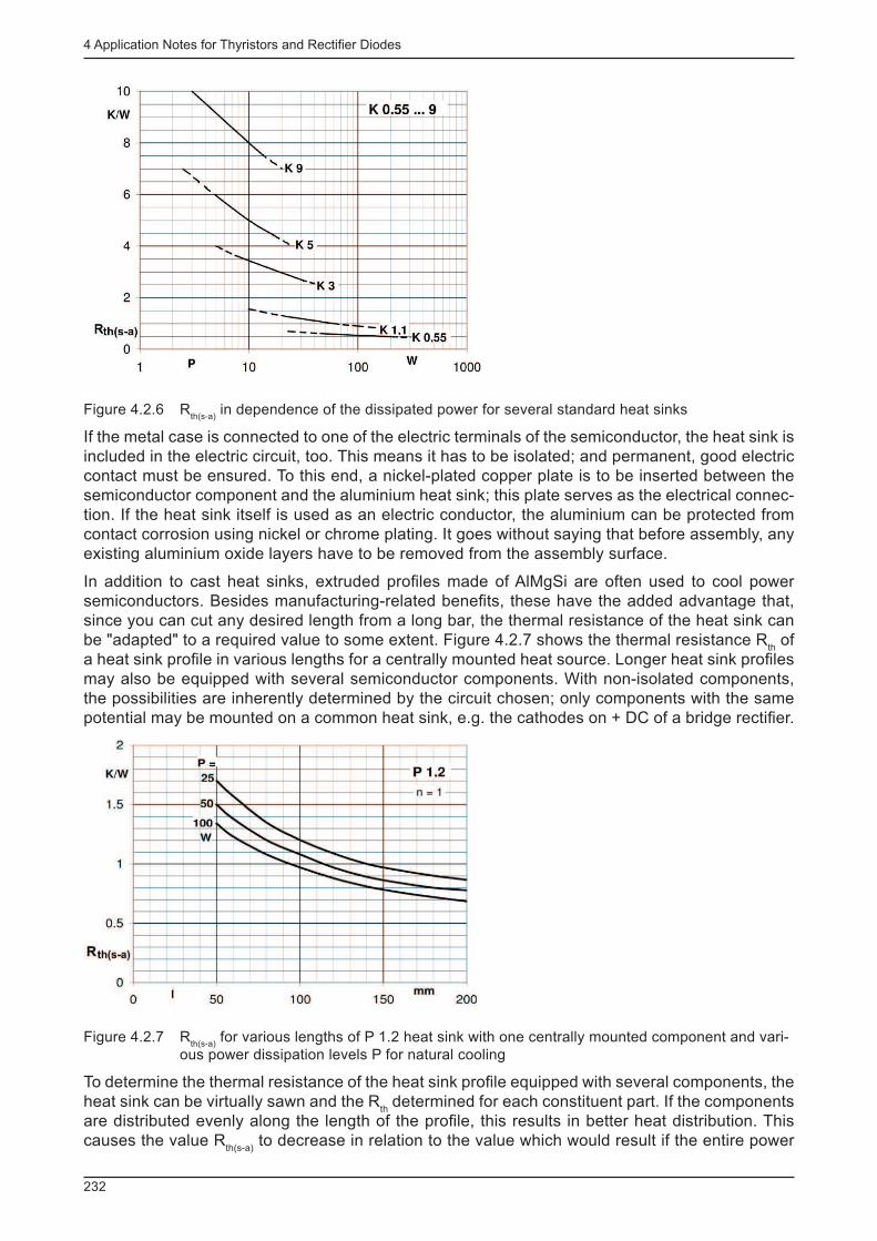
4 Application Notes for Thyristors and Rectifi er Diodes
232
Figure 4.2.6 R th(s-a)
in dependence of the dissipated power for several standard heat sinks
If the metal case is connected to one of the electric terminals of the semiconductor, the heat sink is included in the electric circuit, too. This means it has to be isolated; and permanent, good electric contact must be ensured. To this end, a nickel-plated copper plate is to be inserted between the semiconductor component and the aluminium heat sink; this plate serves as the electrical connec-tion. If the heat sink itself is used as an electric conductor, the aluminium can be protected from contact corrosion using nickel or chrome plating. It goes without saying that before assembly, any existing aluminium oxide layers have to be removed from the assembly surface.
In addition to cast heat sinks, extruded profi les made of AlMgSi are often used to cool power semiconductors. Besides manufacturing-related benefi ts, these have the added advantage that, since you can cut any desired length from a long bar, the thermal resistance of the heat sink can be "adapted" to a required value to some extent. Figure 4.2.7 shows the thermal resistance R
th of
a heat sink profi le in various lengths for a centrally mounted heat source. Longer heat sink profi les may also be equipped with several semiconductor components. With non-isolated components, the possibilities are inherently determined by the circuit chosen; only components with the same potential may be mounted on a common heat sink, e.g. the cathodes on + DC of a bridge rectifi er.
Figure 4.2.7 R th(s-a)
for various lengths of P 1.2 heat sink with one centrally mounted component and vari-ous power dissipation levels P for natural cooling
To determine the thermal resistance of the heat sink profi le equipped with several components, the heat sink can be virtually sawn and the R
th determined for each constituent part. If the components
are distributed evenly along the length of the profi le, this results in better heat distribution. This causes the value R
th(s-a) to decrease in relation to the value which would result if the entire power
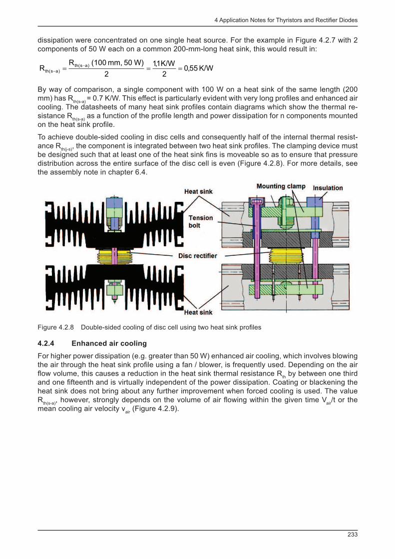
4 Application Notes for Thyristors and Rectifi er Diodes
233
dissipation were concentrated on one single heat source. For the example in Figure 4.2.7 with 2 components of 50 W each on a common 200-mm-long heat sink, this would result in:
K/W55,0
2
K/W1,1
2
W)50mm,(100RR
)as(th
)as(th === --
By way of comparison, a single component with 100 W on a heat sink of the same length (200 mm) has R
th(s-a) = 0.7 K/W. This effect is particularly evident with very long profi les and enhanced air
cooling. The datasheets of many heat sink profi les contain diagrams which show the thermal re-sistance R
th(s-a) as a function of the profi le length and power dissipation for n components mounted
on the heat sink profi le.
To achieve double-sided cooling in disc cells and consequently half of the internal thermal resist-ance R
th(j-s) , the component is integrated between two heat sink profi les. The clamping device must
be designed such that at least one of the heat sink fi ns is moveable so as to ensure that pressure distribution across the entire surface of the disc cell is even (Figure 4.2.8). For more details, see the assembly note in chapter 6.4.
Figure 4.2.8 Double-sided cooling of disc cell using two heat sink profi les
4.2.4 Enhanced air cooling
For higher power dissipation (e.g. greater than 50 W) enhanced air cooling, which involves blowing the air through the heat sink profi le using a fan / blower, is frequently used. Depending on the air fl ow volume, this causes a reduction in the heat sink thermal resistance R
th by between one third
and one fi fteenth and is virtually independent of the power dissipation. Coating or blackening the heat sink does not bring about any further improvement when forced cooling is used. The value R
th(s-a) , however, strongly depends on the volume of air fl owing within the given time V
air /t or the
mean cooling air velocity v air
(Figure 4.2.9).
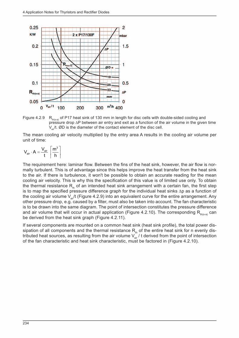
4 Application Notes for Thyristors and Rectifi er Diodes
234
Figure 4.2.9 R th(s-a)
of P17 heat sink of 130 mm in length for disc cells with double-sided cooling and pressure drop ∆P between air entry and exit as a function of the air volume in the given time V
air /t. ØD is the diameter of the contact element of the disc cell.
The mean cooling air velocity multiplied by the entry area A results in the cooling air volume per unit of time:
úû
ùêë
é=×
h
m
t
VAV
3
airair
The requirement here: laminar fl ow. Between the fi ns of the heat sink, however, the air fl ow is nor-mally turbulent. This is of advantage since this helps improve the heat transfer from the heat sink to the air. If there is turbulence, it won't be possible to obtain an accurate reading for the mean cooling air velocity. This is why this the specifi cation of this value is of limited use only. To obtain the thermal resistance R
th of an intended heat sink arrangement with a certain fan, the fi rst step
is to map the specifi ed pressure difference graph for the individual heat sinks ∆p as a function of the cooling air volume V
air /t (Figure 4.2.9) into an equivalent curve for the entire arrangement. Any
other pressure drop, e.g. caused by a fi lter, must also be taken into account. The fan characteristic is to be drawn into the same diagram. The point of intersection constitutes the pressure difference and air volume that will occur in actual application (Figure 4.2.10). The corresponding R
th(s-a) can
be derived from the heat sink graph (Figure 4.2.11).
If several components are mounted on a common heat sink (heat sink profi le), the total power dis-sipation of all components and the thermal resistance R
th of the entire heat sink for n evenly dis-
tributed heat sources, as resulting from the air volume V air
/ t derived from the point of intersection of the fan characteristic and heat sink characteristic, must be factored in (Figure 4.2.10).
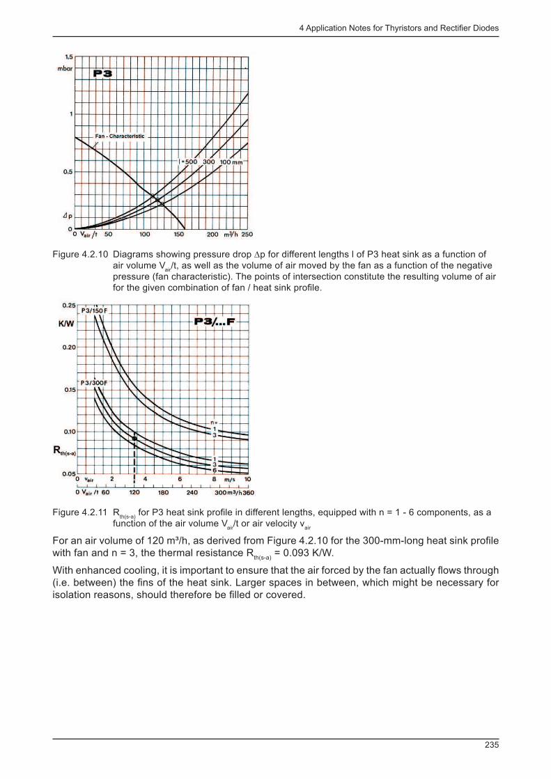
4 Application Notes for Thyristors and Rectifi er Diodes
235
Figure 4.2.10 Diagrams showing pressure drop ∆p for different lengths l of P3 heat sink as a function of air volume V
air /t, as well as the volume of air moved by the fan as a function of the negative
pressure (fan characteristic). The points of intersection constitute the resulting volume of air for the given combination of fan / heat sink profi le.
Figure 4.2.11 R th(s-a)
for P3 heat sink profi le in different lengths, equipped with n = 1 - 6 components, as a function of the air volume V
air /t or air velocity v
air
For an air volume of 120 m³/h, as derived from Figure 4.2.10 for the 300-mm-long heat sink profi le with fan and n = 3, the thermal resistance R
th(s-a) = 0.093 K/W.
With enhanced cooling, it is important to ensure that the air forced by the fan actually fl ows through (i.e. between) the fi ns of the heat sink. Larger spaces in between, which might be necessary for isolation reasons, should therefore be fi lled or covered.
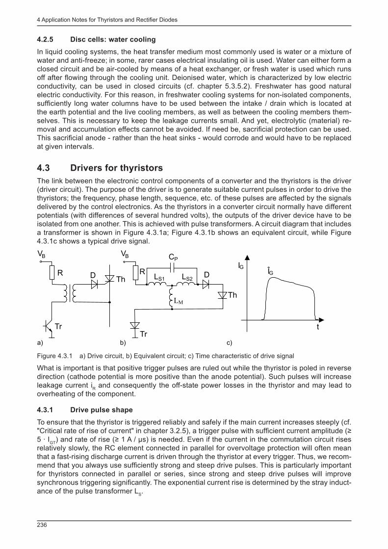
4 Application Notes for Thyristors and Rectifi er Diodes
236
4.2.5 Disc cells: water cooling
In liquid cooling systems, the heat transfer medium most commonly used is water or a mixture of water and anti-freeze; in some, rarer cases electrical insulating oil is used. Water can either form a closed circuit and be air-cooled by means of a heat exchanger, or fresh water is used which runs off after fl owing through the cooling unit. Deionised water, which is characterized by low electric conductivity, can be used in closed circuits (cf. chapter 5.3.5.2). Freshwater has good natural electric conductivity. For this reason, in freshwater cooling systems for non-isolated components, suffi ciently long water columns have to be used between the intake / drain which is located at the earth potential and the live cooling members, as well as between the cooling members them-selves. This is necessary to keep the leakage currents small. And yet, electrolytic (material) re-moval and accumulation effects cannot be avoided. If need be, sacrifi cial protection can be used. This sacrifi cial anode - rather than the heat sinks - would corrode and would have to be replaced at given intervals.
4.3 Drivers for thyristors
The link between the electronic control components of a converter and the thyristors is the driver (driver circuit). The purpose of the driver is to generate suitable current pulses in order to drive the thyristors; the frequency, phase length, sequence, etc. of these pulses are affected by the signals delivered by the control electronics. As the thyristors in a converter circuit normally have different potentials (with differences of several hundred volts), the outputs of the driver device have to be isolated from one another. This is achieved with pulse transformers. A circuit diagram that includes a transformer is shown in Figure 4.3.1a; Figure 4.3.1b shows an equivalent circuit, while Figure 4.3.1c shows a typical drive signal.
Th
Th
D D
TrTr
R RLS1
LM
IG
t
VB
a) b) c)
ÎG
CPVB
LS2
Figure 4.3.1 a) Drive circuit, b) Equivalent circuit; c) Time characteristic of drive signal
What is important is that positive trigger pulses are ruled out while the thyristor is poled in reverse direction (cathode potential is more positive than the anode potential). Such pulses will increase leakage current i
R and consequently the off-state power losses in the thyristor and may lead to
overheating of the component.
4.3.1 Drive pulse shape
To ensure that the thyristor is triggered reliably and safely if the main current increases steeply (cf. "Critical rate of rise of current" in chapter 3.2.5), a trigger pulse with suffi cient current amplitude (≥ 5 · I
GT ) and rate of rise (≥ 1 A / µs) is needed. Even if the current in the commutation circuit rises
relatively slowly, the RC element connected in parallel for overvoltage protection will often mean that a fast-rising discharge current is driven through the thyristor at every trigger. Thus, we recom-mend that you always use suffi ciently strong and steep drive pulses. This is particularly important for thyristors connected in parallel or series, since strong and steep drive pulses will improve synchronous triggering signifi cantly. The exponential current rise is determined by the stray induct-ance of the pulse transformer L
S .
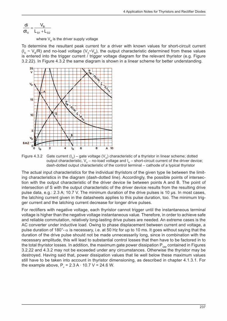
4 Application Notes for Thyristors and Rectifi er Diodes
237
2S1S
B
0 LL
V
dt
di
+=
where V B is the driver supply voltage
To determine the resultant peak current for a driver with known values for short-circuit current (I
K ~ V
B /R) and no-load voltage (V
0 ~V
B ), the output characteristic determined from these values
is entered into the trigger current / trigger voltage diagram for the relevant thyristor (e.g. Figure 3.2.22). In Figure 4.3.2 the same diagram is shown in a linear scheme for better understanding.
Figure 4.3.2 Gate current (I G ) – gate voltage (V
G ) characteristic of a thyristor in linear scheme; dotted
output characteristic, V 0 – no-load voltage and I
K – short-circuit current of the driver device;
dash-dotted output characteristic of the control terminal – cathode of a typical thyristor
The actual input characteristics for the individual thyristors of the given type lie between the limit-ing characteristics in the diagram (dash-dotted line). Accordingly, the possible points of intersec-tion with the output characteristic of the driver device lie between points A and B. The point of intersection of S with the output characteristic of the driver device results from the resulting drive pulse data, e.g.: 2.3 A; 10.7 V. The minimum duration of the drive pulses is 10 µs. In most cases, the latching current given in the datasheets applies to this pulse duration, too. The minimum trig-ger current and the latching current decrease for longer drive pulses.
For rectifi ers with negative voltage, each thyristor cannot trigger until the instantaneous terminal voltage is higher than the negative voltage instantaneous value. Therefore, in order to achieve safe and reliable commutation, relatively long-lasting drive pulses are needed. An extreme cases is the AC converter under inductive load. Owing to phase displacement between current and voltage, a pulse duration of 180°- α is necessary, i.e. at 50 Hz for up to 10 ms. It goes without saying that the duration of the drive pulse should not be made unnecessarily long, since in combination with the necessary amplitude, this will lead to substantial control losses that then have to be factored in to the total thyristor losses. In addition, the maximum gate power dissipation P
GM contained in Figures
3.2.22 and 4.3.2 may not be exceeded under any circumstances. Otherwise the thyristor may be destroyed. Having said that, power dissipation values that lie well below these maximum values still have to be taken into account in thyristor dimensioning, as described in chapter 4.1.3.1. For the example above, P
v = 2.3 A · 10.7 V = 24.6 W.
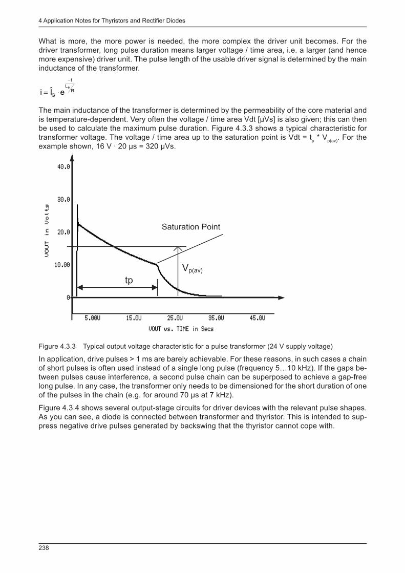
4 Application Notes for Thyristors and Rectifi er Diodes
238
What is more, the more power is needed, the more complex the driver unit becomes. For the driver transformer, long pulse duration means larger voltage / time area, i.e. a larger (and hence more expensive) driver unit. The pulse length of the usable driver signal is determined by the main inductance of the transformer.
R
L
t
G
H
eIi
-
×=
The main inductance of the transformer is determined by the permeability of the core material and is temperature-dependent. Very often the voltage / time area Vdt [µVs] is also given; this can then be used to calculate the maximum pulse duration. Figure 4.3.3 shows a typical characteristic for transformer voltage. The voltage / time area up to the saturation point is Vdt = t
p * V
p(av) . For the
example shown, 16 V · 20 µs = 320 µVs.
Saturation Point
Vp(av)
tp
Figure 4.3.3 Typical output voltage characteristic for a pulse transformer (24 V supply voltage)
In application, drive pulses > 1 ms are barely achievable. For these reasons, in such cases a chain of short pulses is often used instead of a single long pulse (frequency 5…10 kHz). If the gaps be-tween pulses cause interference, a second pulse chain can be superposed to achieve a gap-free long pulse. In any case, the transformer only needs to be dimensioned for the short duration of one of the pulses in the chain (e.g. for around 70 µs at 7 kHz).
Figure 4.3.4 shows several output-stage circuits for driver devices with the relevant pulse shapes. As you can see, a diode is connected between transformer and thyristor. This is intended to sup-press negative drive pulses generated by backswing that the thyristor cannot cope with.
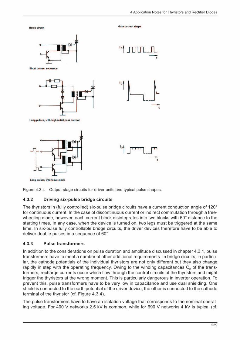
4 Application Notes for Thyristors and Rectifi er Diodes
239
Figure 4.3.4 Output-stage circuits for driver units and typical pulse shapes.
4.3.2 Driving six-pulse bridge circuits
The thyristors in (fully controlled) six-pulse bridge circuits have a current conduction angle of 120° for continuous current. In the case of discontinuous current or indirect commutation through a free-wheeling diode, however, each current block disintegrates into two blocks with 60° distance to the starting times. In any case, when the device is turned on, two legs must be triggered at the same time. In six-pulse fully controllable bridge circuits, the driver devices therefore have to be able to deliver double pulses in a sequence of 60°.
4.3.3 Pulse transformers
In addition to the considerations on pulse duration and amplitude discussed in chapter 4.3.1, pulse transformers have to meet a number of other additional requirements. In bridge circuits, in particu-lar, the cathode potentials of the individual thyristors are not only different but they also change rapidly in step with the operating frequency. Owing to the winding capacitances C
P of the trans-
formers, recharge currents occur which fl ow through the control circuits of the thyristors and might trigger the thyristors at the wrong moment. This is particularly dangerous in inverter operation. To prevent this, pulse transformers have to be very low in capacitance and use dual shielding. One shield is connected to the earth potential of the driver device; the other is connected to the cathode terminal of the thyristor (cf. Figure 4.3.4).
The pulse transformers have to have an isolation voltage that corresponds to the nominal operat-ing voltage. For 400 V networks 2.5 kV is common, while for 690 V networks 4 kV is typical (cf.
4 Application Notes for Thyristors and Rectifi er Diodes
240
EN 50178). In accordance with the isolation voltage, the transformers must demonstrate the cor-responding air and creepage distances between the terminals (IEC 60664).
Winding conditions other than 1:1 will enable level adjustments between primary and secondary side. Further common ratios are 2:1 or 3:1.
4.3.4 Pulse generation
To generate drive pulses, enable phase comparison with the terminal voltage, synchronisation, etc. integrated circuits are used which greatly facilitate the design of driver devices. Owing to the power that can be dissipated by an integrated circuit, however, it is not possible to directly extract a drive pulse with suffi cient power. Rather, an output amplifi er stage has to be added between IC output and driver transformer.
An important requirement here is drive pulse symmetry. Any asymmetry generates additional har-monic content and DC current components. On the other hand, the harmonics and voltage peaks (commutation notches and turn-off overvoltage) generated by the working converter itself must not infl uence the function of the driver device. Thus, suffi cient decoupling is to be ensured.
4.4 Fault behaviour and diode / thyristor protection
4.4.1 General voltage surge protection
Semiconductor components are known for being sensitive to overvoltage. If the maximum rated voltages given in the datasheet are exceeded, the component might be destroyed. For this rea-son, the components have to be protected from any excess voltage that might occur in any of the circuits, i.e. the voltage surges have to be reduced to levels which are below the maximum rated values for the given component. Resistors and capacitors (RC elements), as well as certain semi-conductor components such as varistors and silicon avalanche diodes have proven to be a reliable way of ensuring this.
The use of RC networks turns the inductors in the circuit to series resonant circuits, converting the steeply increasing voltage peaks into attenuated oscillations of low amplitude. As a result, the energy of the overvoltage is forced to decrease at low level over an extended period of time, rather than within a brief period of time at high power.
All of the remaining aforementioned circuit components make use of the non-linear resistance behaviour. Their internal resistances decrease as the voltage increases. In combination with the circuit resistors and inductors, these form non-linear voltage dividers which let through the low voltages almost without attenuation, while higher voltages above a certain level are strongly at-tenuated. Here, too, the overvoltage energy is distributed over a longer period; it is almost fully absorbed by the damping components alone.
The overvoltage protection components can be integrated on the AC side of the switch assembly, on the DC side or parallel to the individual switches. The advantages and disadvantages of the different arrangements will be discussed separately for each individual circuit component.
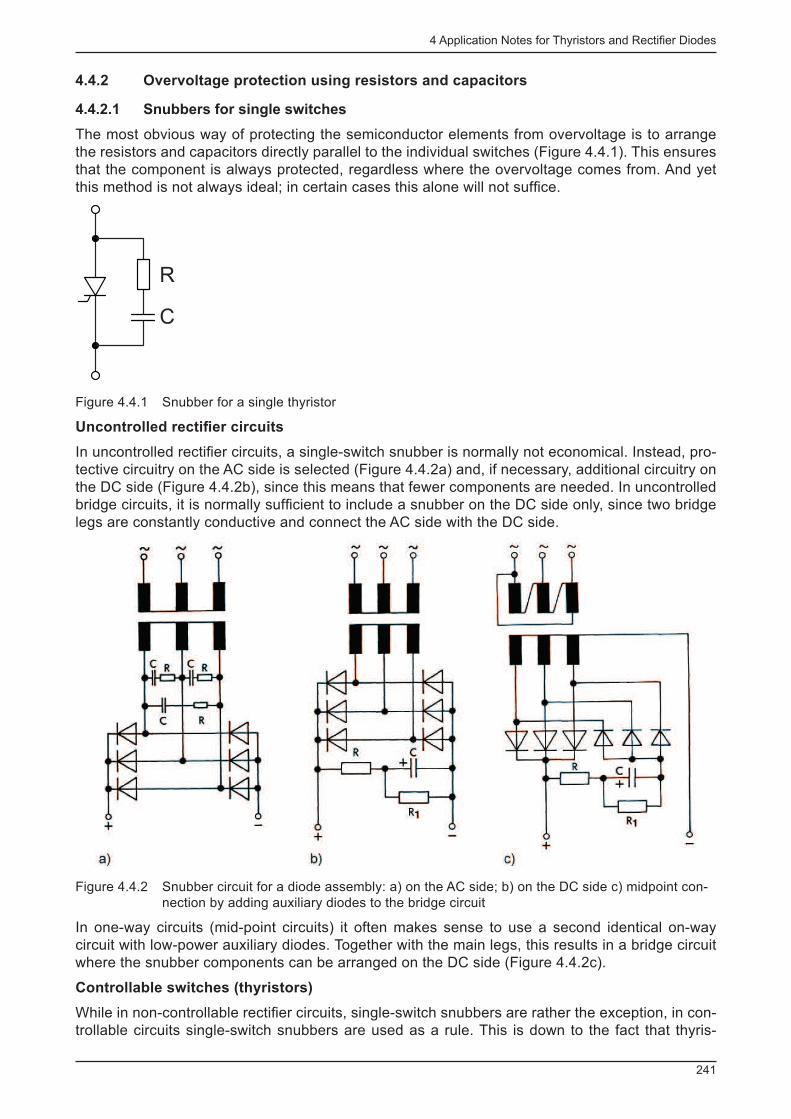
4 Application Notes for Thyristors and Rectifi er Diodes
241
4.4.2 Overvoltage protection using resistors and capacitors
4.4.2.1 Snubbers for single switches
The most obvious way of protecting the semiconductor elements from overvoltage is to arrange the resistors and capacitors directly parallel to the individual switches (Figure 4.4.1). This ensures that the component is always protected, regardless where the overvoltage comes from. And yet this method is not always ideal; in certain cases this alone will not suffi ce.
R
C
Figure 4.4.1 Snubber for a single thyristor
Uncontrolled rectifi er circuits
In uncontrolled rectifi er circuits, a single-switch snubber is normally not economical. Instead, pro-tective circuitry on the AC side is selected (Figure 4.4.2a) and, if necessary, additional circuitry on the DC side (Figure 4.4.2b), since this means that fewer components are needed. In uncontrolled bridge circuits, it is normally suffi cient to include a snubber on the DC side only, since two bridge legs are constantly conductive and connect the AC side with the DC side.
Figure 4.4.2 Snubber circuit for a diode assembly: a) on the AC side; b) on the DC side c) midpoint con-nection by adding auxiliary diodes to the bridge circuit
In one-way circuits (mid-point circuits) it often makes sense to use a second identical on-way circuit with low-power auxiliary diodes. Together with the main legs, this results in a bridge circuit where the snubber components can be arranged on the DC side (Figure 4.4.2c).
Controllable switches (thyristors)
While in non-controllable rectifi er circuits, single-switch snubbers are rather the exception, in con-trollable circuits single-switch snubbers are used as a rule. This is down to the fact that thyris-
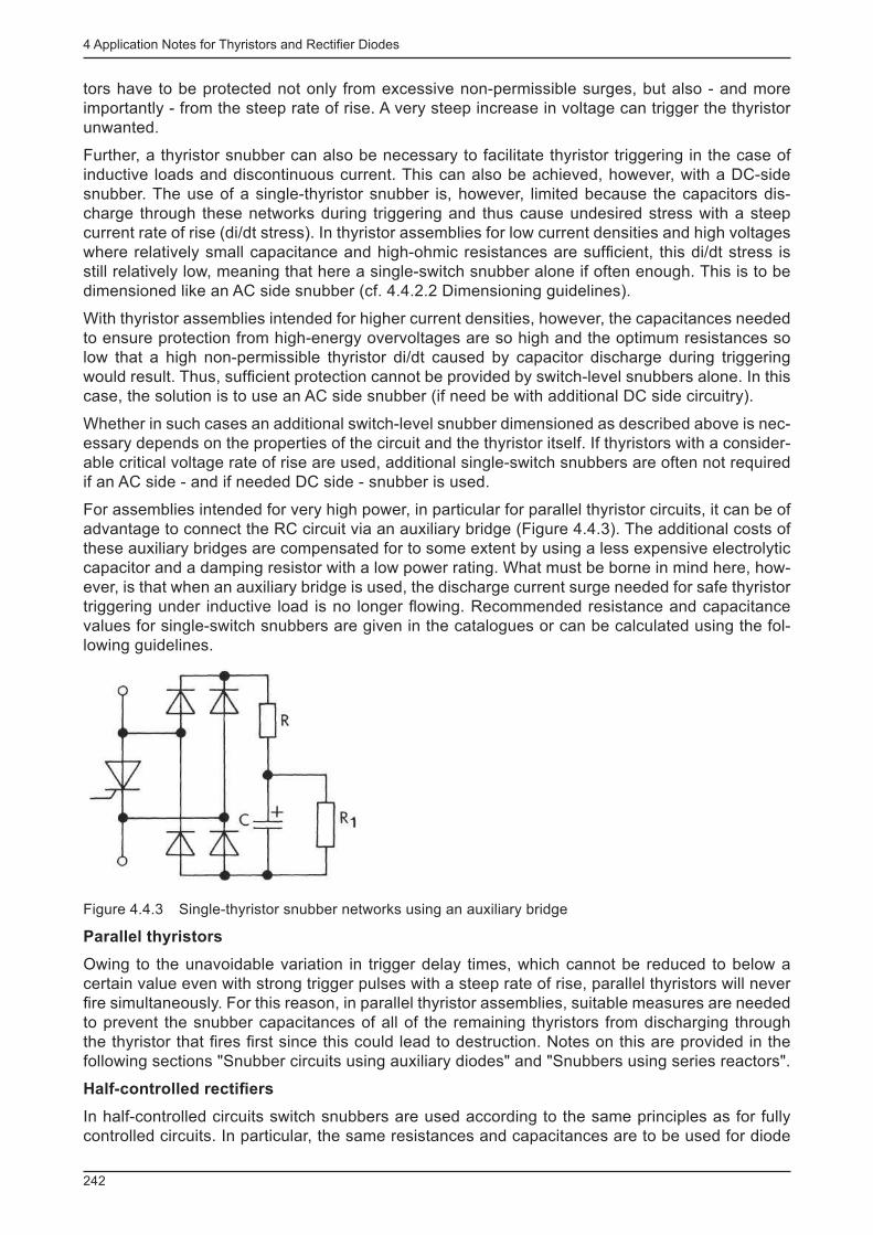
4 Application Notes for Thyristors and Rectifi er Diodes
242
tors have to be protected not only from excessive non-permissible surges, but also - and more importantly - from the steep rate of rise. A very steep increase in voltage can trigger the thyristor unwanted.
Further, a thyristor snubber can also be necessary to facilitate thyristor triggering in the case of inductive loads and discontinuous current. This can also be achieved, however, with a DC-side snubber. The use of a single-thyristor snubber is, however, limited because the capacitors dis-charge through these networks during triggering and thus cause undesired stress with a steep current rate of rise (di/dt stress). In thyristor assemblies for low current densities and high voltages where relatively small capacitance and high-ohmic resistances are suffi cient, this di/dt stress is still relatively low, meaning that here a single-switch snubber alone if often enough. This is to be dimensioned like an AC side snubber (cf. 4.4.2.2 Dimensioning guidelines).
With thyristor assemblies intended for higher current densities, however, the capacitances needed to ensure protection from high-energy overvoltages are so high and the optimum resistances so low that a high non-permissible thyristor di/dt caused by capacitor discharge during triggering would result. Thus, suffi cient protection cannot be provided by switch-level snubbers alone. In this case, the solution is to use an AC side snubber (if need be with additional DC side circuitry).
Whether in such cases an additional switch-level snubber dimensioned as described above is nec-essary depends on the properties of the circuit and the thyristor itself. If thyristors with a consider-able critical voltage rate of rise are used, additional single-switch snubbers are often not required if an AC side - and if needed DC side - snubber is used.
For assemblies intended for very high power, in particular for parallel thyristor circuits, it can be of advantage to connect the RC circuit via an auxiliary bridge (Figure 4.4.3). The additional costs of these auxiliary bridges are compensated for to some extent by using a less expensive electrolytic capacitor and a damping resistor with a low power rating. What must be borne in mind here, how-ever, is that when an auxiliary bridge is used, the discharge current surge needed for safe thyristor triggering under inductive load is no longer fl owing. Recommended resistance and capacitance values for single-switch snubbers are given in the catalogues or can be calculated using the fol-lowing guidelines.
Figure 4.4.3 Single-thyristor snubber networks using an auxiliary bridge
Parallel thyristors
Owing to the unavoidable variation in trigger delay times, which cannot be reduced to below a certain value even with strong trigger pulses with a steep rate of rise, parallel thyristors will never fi re simultaneously. For this reason, in parallel thyristor assemblies, suitable measures are needed to prevent the snubber capacitances of all of the remaining thyristors from discharging through the thyristor that fi res fi rst since this could lead to destruction. Notes on this are provided in the following sections "Snubber circuits using auxiliary diodes" and "Snubbers using series reactors".
Half-controlled rectifi ers
In half-controlled circuits switch snubbers are used according to the same principles as for fully controlled circuits. In particular, the same resistances and capacitances are to be used for diode

4 Application Notes for Thyristors and Rectifi er Diodes
243
snubber circuits as for thyristor snubbers. Under no circumstances are the snubber circuit ele-ments intended for pure diode assemblies suffi cient.
Freewheeling paths
Freewheeling diodes or silicon diodes in freewheeling paths of controllable converter circuits are to be protected just like the thyristors in the main legs.
Dimensioning guidelines for single-switch snubbers
The following dimensioning guidelines for single-switch snubbers apply on condition that the snub-ber circuit is only intended to provide protection from the overvoltages caused by the hole stor-age effect (HSE). If additional high-energy overvoltages, for example those that occur when the freewheeling transformer is turned off, have to be attenuated, the resistances and capacitances are to be calculated on the basis of the guidelines described in chapter 4.4.2.2 AC side snubbers / Dimensioning guidelines.
On the assumption that around half of the energy represented by the recovered charge Q rr is trans-
ferred to the circuit in the form of an overvoltage, the most favourable values for capacitance and attenuating resistance R can be calculated as
2V
QC
v
rr
×=
C
LR s=
C: Capacitance (in µF); LS: Total inductance in the circuit (in µH);
R: Resistance (in Ω); Vv: Effective terminal voltage (in V);
Q rr : Recovered charge (in µC).
In addition, it should be considered that the current amplitude during discharge of C via R and the thyristor must not be greater than 50 A; the amount is determined by the voltage at the moment of fi ring and the resistance R. If need be, the value for R has to be selected above the value that results from the equation above. The resulting overvoltage damping is, of course, not quite as favourable. The power dissipation P
R imin the damping resistor R can be calculated using the following for-
mula:
fVCkfQV2P 2
V1rrVR ×××+×××= k
1 = 0 for switches in uncontrolled rectifi er circuits
k 1 = 2·10 -6 for switches in controlled single-pulse and double-pulse midpoint circuits, as well as
half-controlled two-pulse bridge circuits and AC controllers k
1 = 3·10 -6 for switches in controlled three-pulse and six-pulse midpoint circuits, as well as
fully-controlled two-pulse bridge circuits and AC controllers k
1 = 4·10 -6 for switches in controlled six-pulse bridge circuits
Q rr : Recovered charge (in C; not µC!)
V v : Effective terminal voltage (in V)
f: Operating frequency (in Hz) C: Capacitance (in µF)
When selecting the resistor, please note that the rating specifi ed by the manufacturer may refer to various surface temperatures. It is advisable to dimension for a surface temperature of max. 200°C.
Snubber circuits using auxiliary diodes
In some cases, it is possible or even necessary to use auxiliary diodes in the snubber circuits when connecting thyristors with RC elements. For example, using the circuit shown in Figure 4.4.4a, the rate of rise of the forward blocking voltage can be ideally attenuated by the components R and C, while for discharge of capacitor C during thyristor triggering an additional resistance R
z is effective
which limits the current surge to a harmless level. In reverse direction, R z is effective too, meaning
that in this direction the reduction of surge voltages is not ideal.
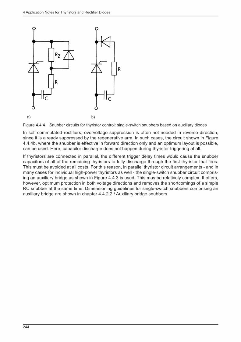
4 Application Notes for Thyristors and Rectifi er Diodes
244
Figure 4.4.4 Snubber circuits for thyristor control: single-switch snubbers based on auxiliary diodes
In self-commutated rectifi ers, overvoltage suppression is often not needed in reverse direction, since it is already suppressed by the regenerative arm. In such cases, the circuit shown in Figure 4.4.4b, where the snubber is effective in forward direction only and an optimum layout is possible, can be used. Here, capacitor discharge does not happen during thyristor triggering at all.
If thyristors are connected in parallel, the different trigger delay times would cause the snubber capacitors of all of the remaining thyristors to fully discharge through the fi rst thyristor that fi res. This must be avoided at all costs. For this reason, in parallel thyristor circuit arrangements - and in many cases for individual high-power thyristors as well - the single-switch snubber circuit compris-ing an auxiliary bridge as shown in Figure 4.4.3 is used. This may be relatively complex. It offers, however, optimum protection in both voltage directions and removes the shortcomings of a simple RC snubber at the same time. Dimensioning guidelines for single-switch snubbers comprising an auxiliary bridge are shown in chapter 4.4.2.2 / Auxiliary bridge snubbers.
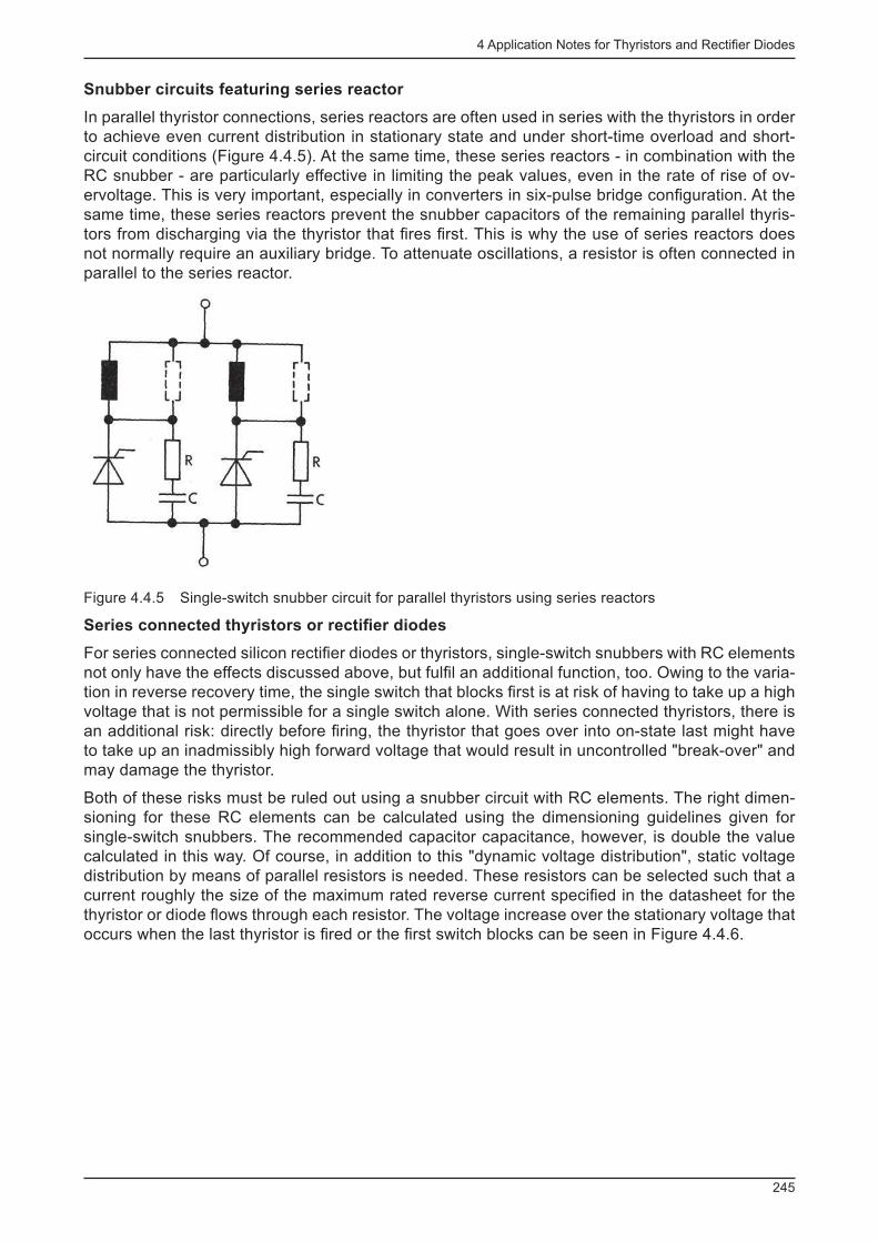
4 Application Notes for Thyristors and Rectifi er Diodes
245
Snubber circuits featuring series reactor
In parallel thyristor connections, series reactors are often used in series with the thyristors in order to achieve even current distribution in stationary state and under short-time overload and short-circuit conditions (Figure 4.4.5). At the same time, these series reactors - in combination with the RC snubber - are particularly effective in limiting the peak values, even in the rate of rise of ov-ervoltage. This is very important, especially in converters in six-pulse bridge confi guration. At the same time, these series reactors prevent the snubber capacitors of the remaining parallel thyris-tors from discharging via the thyristor that fi res fi rst. This is why the use of series reactors does not normally require an auxiliary bridge. To attenuate oscillations, a resistor is often connected in parallel to the series reactor.
Figure 4.4.5 Single-switch snubber circuit for parallel thyristors using series reactors
Series connected thyristors or rectifi er diodes
For series connected silicon rectifi er diodes or thyristors, single-switch snubbers with RC elements not only have the effects discussed above, but fulfi l an additional function, too. Owing to the varia-tion in reverse recovery time, the single switch that blocks fi rst is at risk of having to take up a high voltage that is not permissible for a single switch alone. With series connected thyristors, there is an additional risk: directly before fi ring, the thyristor that goes over into on-state last might have to take up an inadmissibly high forward voltage that would result in uncontrolled "break-over" and may damage the thyristor.
Both of these risks must be ruled out using a snubber circuit with RC elements. The right dimen-sioning for these RC elements can be calculated using the dimensioning guidelines given for single-switch snubbers. The recommended capacitor capacitance, however, is double the value calculated in this way. Of course, in addition to this "dynamic voltage distribution", static voltage distribution by means of parallel resistors is needed. These resistors can be selected such that a current roughly the size of the maximum rated reverse current specifi ed in the datasheet for the thyristor or diode fl ows through each resistor. The voltage increase over the stationary voltage that occurs when the last thyristor is fi red or the fi rst switch blocks can be seen in Figure 4.4.6.
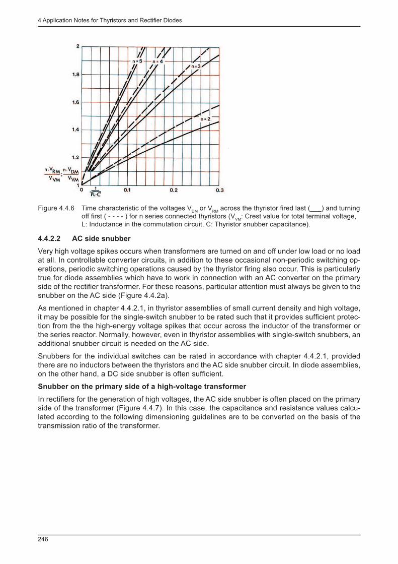
4 Application Notes for Thyristors and Rectifi er Diodes
246
Figure 4.4.6 Time characteristic of the voltages V DM
or V RM
across the thyristor fi red last (___) and turning off fi rst ( - - - - ) for n series connected thyristors (V
VM : Crest value for total terminal voltage,
L: Inductance in the commutation circuit, C: Thyristor snubber capacitance).
4.4.2.2 AC side snubber
Very high voltage spikes occurs when transformers are turned on and off under low load or no load at all. In controllable converter circuits, in addition to these occasional non-periodic switching op-erations, periodic switching operations caused by the thyristor fi ring also occur. This is particularly true for diode assemblies which have to work in connection with an AC converter on the primary side of the rectifi er transformer. For these reasons, particular attention must always be given to the snubber on the AC side (Figure 4.4.2a).
As mentioned in chapter 4.4.2.1, in thyristor assemblies of small current density and high voltage, it may be possible for the single-switch snubber to be rated such that it provides suffi cient protec-tion from the the high-energy voltage spikes that occur across the inductor of the transformer or the series reactor. Normally, however, even in thyristor assemblies with single-switch snubbers, an additional snubber circuit is needed on the AC side.
Snubbers for the individual switches can be rated in accordance with chapter 4.4.2.1, provided there are no inductors between the thyristors and the AC side snubber circuit. In diode assemblies, on the other hand, a DC side snubber is often suffi cient.
Snubber on the primary side of a high-voltage transformer
In rectifi ers for the generation of high voltages, the AC side snubber is often placed on the primary side of the transformer (Figure 4.4.7). In this case, the capacitance and resistance values calcu-lated according to the following dimensioning guidelines are to be converted on the basis of the transmission ratio of the transformer.

4 Application Notes for Thyristors and Rectifi er Diodes
247
Figure 4.4.7 Primary-side snubber of a high-voltage transformer
Dimensioning guidelines for AC side snubbers
The most favourable values for capacitance C and damping resistance R can be calculated ap-proximately using the following formulae:
2
V2
T
Vfk
P170C
×××e
×=
33 10fC
kR ×
×=
The power dissipation P v in the resistor R can be approximated with
10222
V2V 10RCfVk2,1P -××××××= [W] P
T [VA]: Transformer power rating; ε [%]: Relative magnetising current of the
transformer; V v [V]: AC voltage effective at the RC element; C [µF]: Capacitance;
R [Ω]: Resistance; f [Hz]: Frequency, for k
2 the following values are to be used:
k 2 = 1 for all single-phase circuits
k 2 = 2 for three-phase circuits and snubber on the DC side or using
an auxiliary bridge k
2 = 3 for three-phase circuits and snubber on the AC side
The factor k 3 can be seen in Figure 4.4.8a as a function of the rated power of the transformer P
T .
If the magnetising current ε of the transformer is not known, approximated values as a function of P
T can be derived from Figure 4.4.8b.
Figure 4.4.8 a) Factor k 3 as a function of the rated power P
T of the converter transformer; b) Magnetising
current ε (as a percentage of the rated current) of a converter transformer as a function of its rated power P
T .
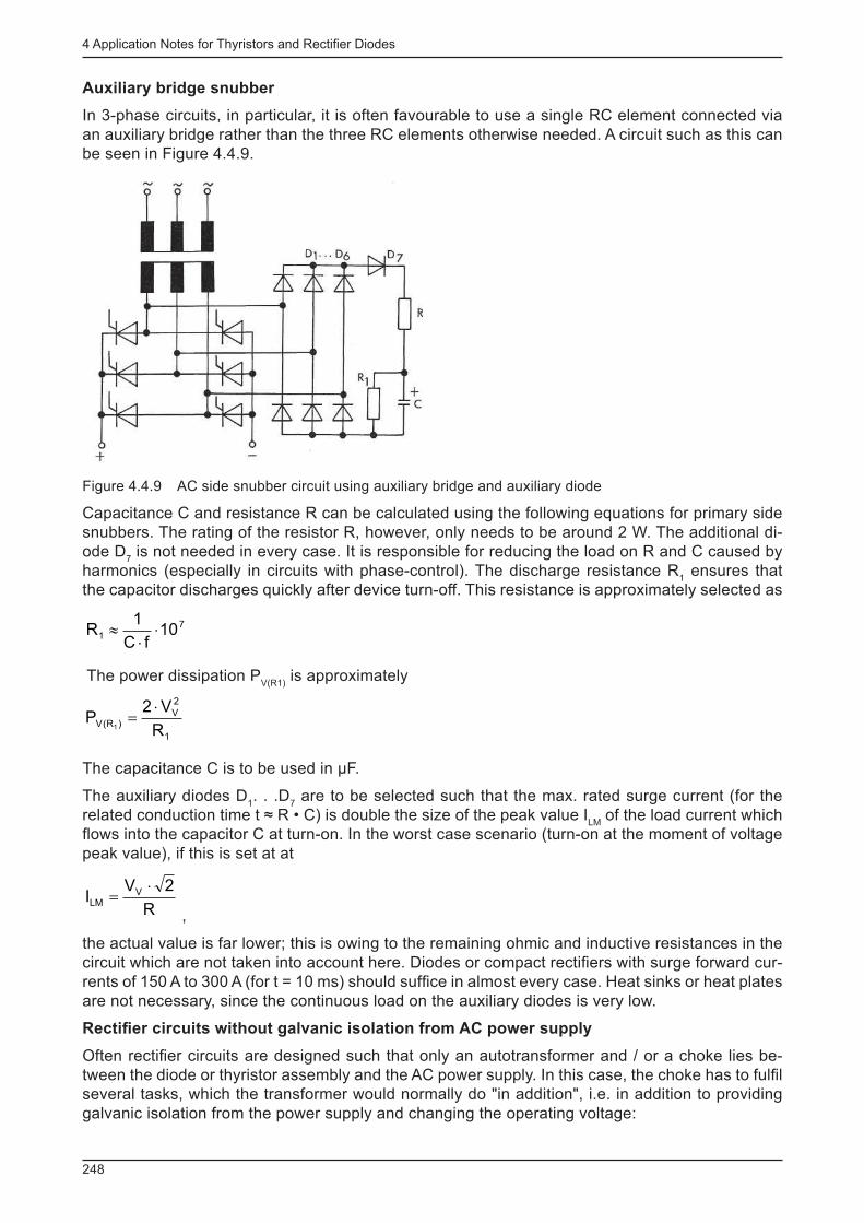
4 Application Notes for Thyristors and Rectifi er Diodes
248
Auxiliary bridge snubber
In 3-phase circuits, in particular, it is often favourable to use a single RC element connected via an auxiliary bridge rather than the three RC elements otherwise needed. A circuit such as this can be seen in Figure 4.4.9.
Figure 4.4.9 AC side snubber circuit using auxiliary bridge and auxiliary diode
Capacitance C and resistance R can be calculated using the following equations for primary side snubbers. The rating of the resistor R, however, only needs to be around 2 W. The additional di-ode D
7 is not needed in every case. It is responsible for reducing the load on R and C caused by
harmonics (especially in circuits with phase-control). The discharge resistance R 1 ensures that
the capacitor discharges quickly after device turn-off. This resistance is approximately selected as
7
1 10fC
1R ×
×»
The power dissipation P V(R1)
is approximately
1
2
V)R(V
R
V2P
1
×=
The capacitance C is to be used in µF.
The auxiliary diodes D 1 . . .D
7 are to be selected such that the max. rated surge current (for the
related conduction time t ≈ R • C) is double the size of the peak value I LM
of the load current which fl ows into the capacitor C at turn-on. In the worst case scenario (turn-on at the moment of voltage peak value), if this is set at at
R
2VI VLM
×=
,
the actual value is far lower; this is owing to the remaining ohmic and inductive resistances in the circuit which are not taken into account here. Diodes or compact rectifi ers with surge forward cur-rents of 150 A to 300 A (for t = 10 ms) should suffi ce in almost every case. Heat sinks or heat plates are not necessary, since the continuous load on the auxiliary diodes is very low.
Rectifi er circuits without galvanic isolation from AC power supply
Often rectifi er circuits are designed such that only an autotransformer and / or a choke lies be-tween the diode or thyristor assembly and the AC power supply. In this case, the choke has to fulfi l several tasks, which the transformer would normally do "in addition", i.e. in addition to providing galvanic isolation from the power supply and changing the operating voltage:
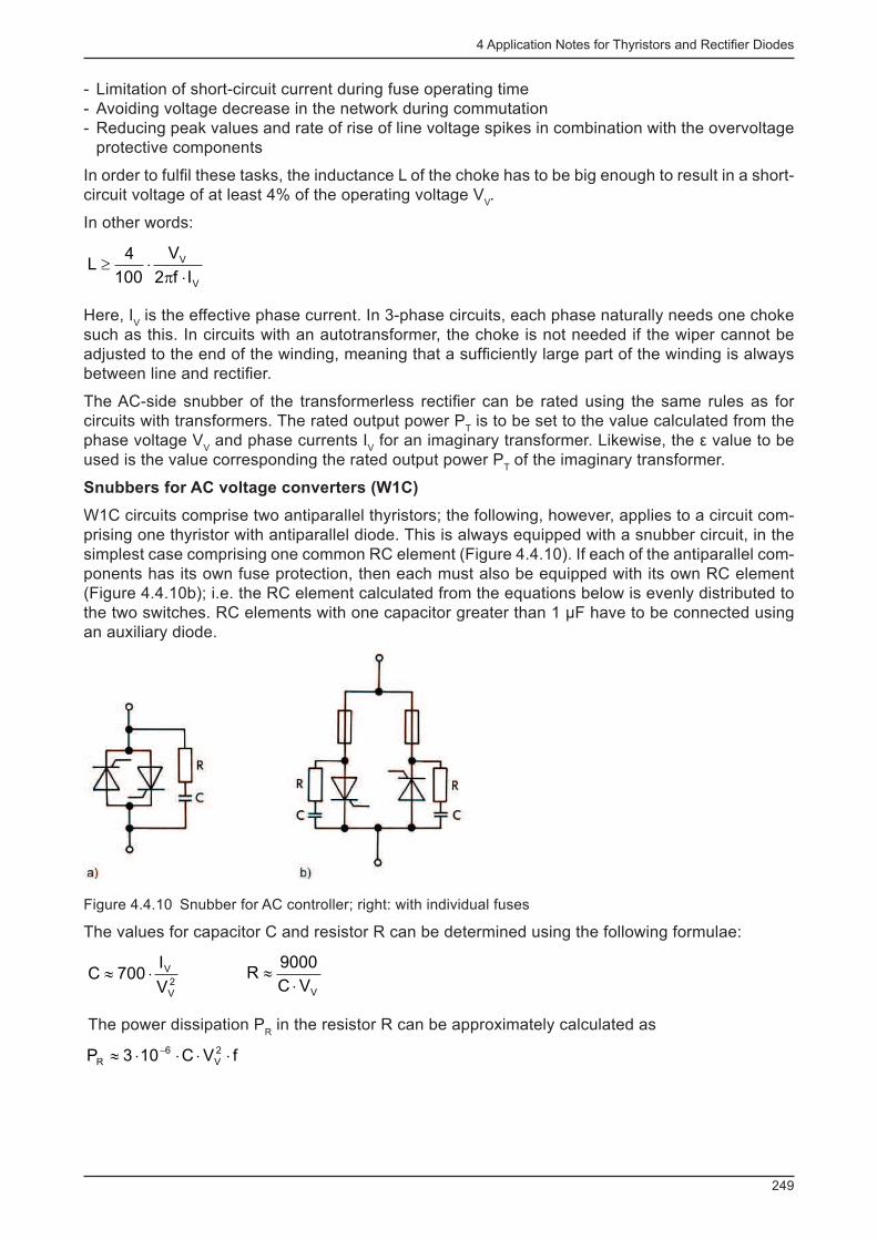
4 Application Notes for Thyristors and Rectifi er Diodes
249
- Limitation of short-circuit current during fuse operating time - Avoiding voltage decrease in the network during commutation - Reducing peak values and rate of rise of line voltage spikes in combination with the overvoltage protective components
In order to fulfi l these tasks, the inductance L of the choke has to be big enough to result in a short-circuit voltage of at least 4% of the operating voltage V
V .
In other words:
V
V
If2
V
100
4L
×p׳
Here, I V is the effective phase current. In 3-phase circuits, each phase naturally needs one choke
such as this. In circuits with an autotransformer, the choke is not needed if the wiper cannot be adjusted to the end of the winding, meaning that a suffi ciently large part of the winding is always between line and rectifi er.
The AC-side snubber of the transformerless rectifi er can be rated using the same rules as for circuits with transformers. The rated output power P
T is to be set to the value calculated from the
phase voltage V V and phase currents I
V for an imaginary transformer. Likewise, the ε value to be
used is the value corresponding the rated output power P T of the imaginary transformer.
Snubbers for AC voltage converters (W1C)
W1C circuits comprise two antiparallel thyristors; the following, however, applies to a circuit com-prising one thyristor with antiparallel diode. This is always equipped with a snubber circuit, in the simplest case comprising one common RC element (Figure 4.4.10). If each of the antiparallel com-ponents has its own fuse protection, then each must also be equipped with its own RC element (Figure 4.4.10b); i.e. the RC element calculated from the equations below is evenly distributed to the two switches. RC elements with one capacitor greater than 1 µF have to be connected using an auxiliary diode.
Figure 4.4.10 Snubber for AC controller; right: with individual fuses
The values for capacitor C and resistor R can be determined using the following formulae:
2
V
V
V
I700C ×»
VVC
9000R
×»
The power dissipation P R in the resistor R can be approximately calculated as
fVC103P 2
V
6
R ××××» -
4 Application Notes for Thyristors and Rectifi er Diodes
250
4.4.2.3 DC side snubber circuits
Diode assemblies
As mentioned several times already, for diode assemblies in bridge confi gurations it is normally enough to add a snubber to the DC side if the diode assemblies are not already connected to a low-inductance voltage DC link. The resistors and capacitors are rated either according to the guidelines provided in chapter 4.4.2.2 or in this chapter, depending on whether the surge voltages to be attenuated are on the AC or DC side. If there is any possibility of the rectifi er being conduc-tive even when the load is turned off or disconnected, a discharge resistor has to be used.
In rectifi ers with permanent capacitive load, this load will function as an overvoltage snubber, meaning that no additional snubber circuits are needed. If, on the other hand, there is a ripple fi lter choke or fuse between the rectifi er and capacitive load, a snubber circuit for overvoltage will have to be integrated directly at the rectifi er in addition.
For diode assemblies in midpoint confi gurations, it often makes sense to set up the snubber similar to an AC-side snubber with auxiliary bridge, with one half of the auxiliary bridge being formed by the principal arms of the rectifi er. Small auxiliary diodes are added to the other half of the auxiliary bridge. Note that the resistors and capacitors, as well as the auxiliary diodes are to be rated in the same way as for an AC-side snubber. What must be borne in mind, however, is that such snubbers do not provide protection from overvoltages that affect the rectifi er from the DC side.
Thyristor assemblies
In thyristor assemblies, an AC-side snubber and single-switch snubbers will normally be integrat-ed, meaning DC snubbers can often be dispensed with. In individual cases, however, they might still be necessary. Sometimes, the single-switch snubbers are not necessary and one DC and one AC side snubber can be used instead. The latter functions as a capacitive base load at the same time, ensuring that the thyristors fi re without any problems under unfavourable operating condi-tions. The capacitor and resistor value can be calculated according to the following "dimensioning guidelines".
Inverters
In inverters, a battery or buffer capacitor is often connected on the DC side, meaning no DC snub-ber circuit is needed.
Dimensioning guidelines
The best effect is achieved if the following conditions are fulfi lled:
C
L2RR L
L ×=+
(Figure 4.4.2b). If
R = R L
is selected, this results in
2
L
L
R
LC =
L L : Load inductance (in µH);
R L : Ohmic resistance in the load (in Ω);
C: Snubber capacitance (in µF); R: Damping resistance (in Ω).
In many cases, it will suffi ce to use a smaller capacitor. In this case, R should be selected such that the aforementioned equation applies approximately.
The power dissipation P V in the damping resistor R can be calculated as
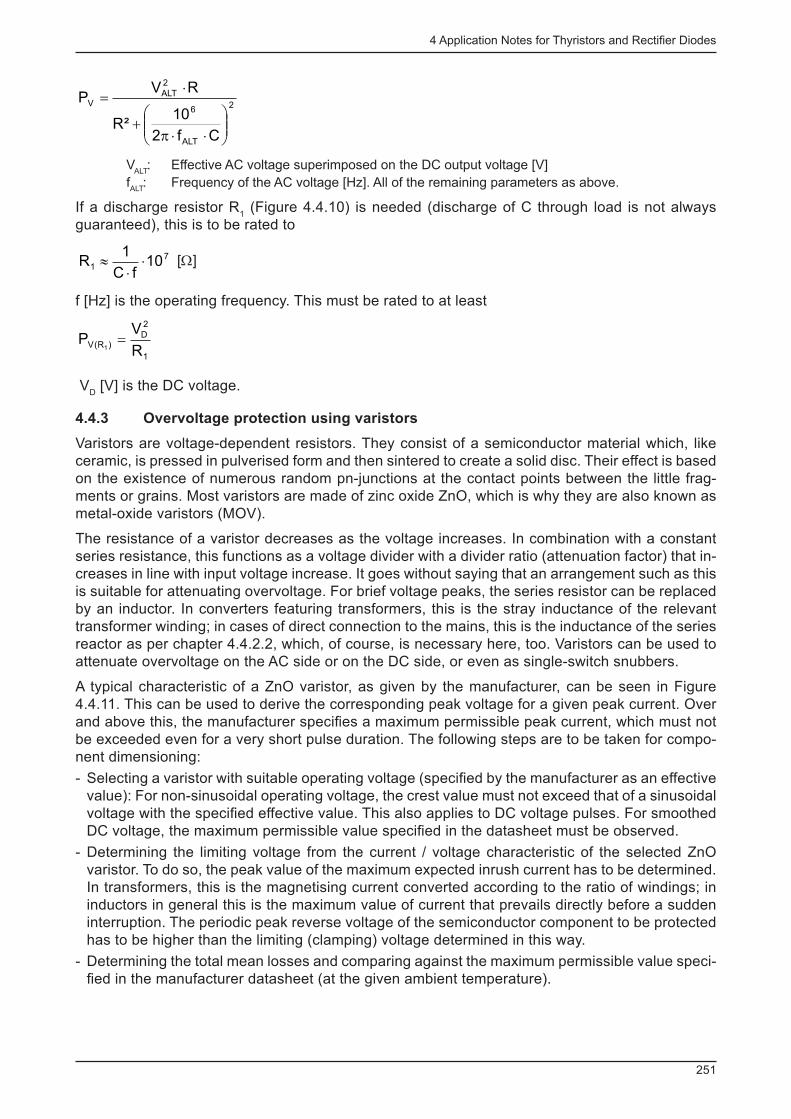
4 Application Notes for Thyristors and Rectifi er Diodes
251
2
ALT
6
2
ALTV
Cf2
10²R
RVP
÷÷ø
öççè
æ××p
+
×=
V ALT
: Effective AC voltage superimposed on the DC output voltage [V] f ALT
: Frequency of the AC voltage [Hz]. All of the remaining parameters as above.
If a discharge resistor R 1 (Figure 4.4.10) is needed (discharge of C through load is not always
guaranteed), this is to be rated to
7
1 10fC
1R ×
×» [Ω]
f [Hz] is the operating frequency. This must be rated to at least
1
2
D)R(V
R
VP
1=
V D [V] is the DC voltage.
4.4.3 Overvoltage protection using varistors
Varistors are voltage-dependent resistors. They consist of a semiconductor material which, like ceramic, is pressed in pulverised form and then sintered to create a solid disc. Their effect is based on the existence of numerous random pn-junctions at the contact points between the little frag-ments or grains. Most varistors are made of zinc oxide ZnO, which is why they are also known as metal-oxide varistors (MOV).
The resistance of a varistor decreases as the voltage increases. In combination with a constant series resistance, this functions as a voltage divider with a divider ratio (attenuation factor) that in-creases in line with input voltage increase. It goes without saying that an arrangement such as this is suitable for attenuating overvoltage. For brief voltage peaks, the series resistor can be replaced by an inductor. In converters featuring transformers, this is the stray inductance of the relevant transformer winding; in cases of direct connection to the mains, this is the inductance of the series reactor as per chapter 4.4.2.2, which, of course, is necessary here, too. Varistors can be used to attenuate overvoltage on the AC side or on the DC side, or even as single-switch snubbers.
A typical characteristic of a ZnO varistor, as given by the manufacturer, can be seen in Figure 4.4.11. This can be used to derive the corresponding peak voltage for a given peak current. Over and above this, the manufacturer specifi es a maximum permissible peak current, which must not be exceeded even for a very short pulse duration. The following steps are to be taken for compo-nent dimensioning:
- Selecting a varistor with suitable operating voltage (specifi ed by the manufacturer as an effective value): For non-sinusoidal operating voltage, the crest value must not exceed that of a sinusoidal voltage with the specifi ed effective value. This also applies to DC voltage pulses. For smoothed DC voltage, the maximum permissible value specifi ed in the datasheet must be observed.
- Determining the limiting voltage from the current / voltage characteristic of the selected ZnO varistor. To do so, the peak value of the maximum expected inrush current has to be determined. In transformers, this is the magnetising current converted according to the ratio of windings; in inductors in general this is the maximum value of current that prevails directly before a sudden interruption. The periodic peak reverse voltage of the semiconductor component to be protected has to be higher than the limiting (clamping) voltage determined in this way.
- Determining the total mean losses and comparing against the maximum permissible value speci-fi ed in the manufacturer datasheet (at the given ambient temperature).
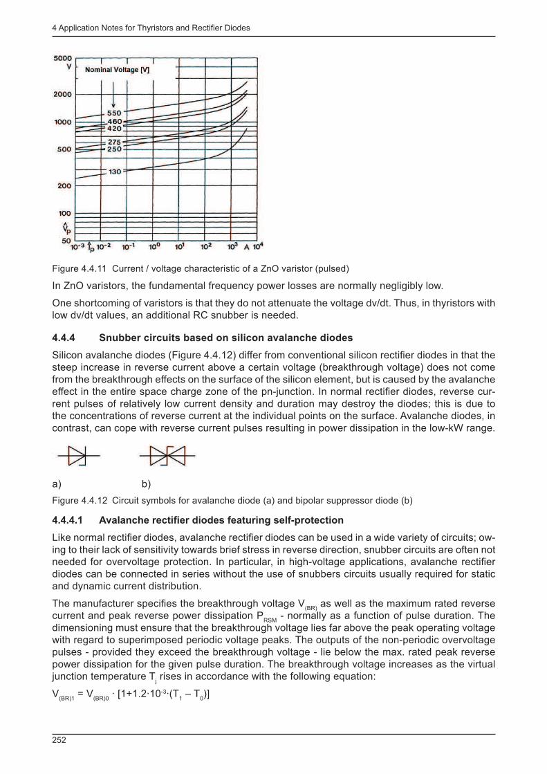
4 Application Notes for Thyristors and Rectifi er Diodes
252
Figure 4.4.11 Current / voltage characteristic of a ZnO varistor (pulsed)
In ZnO varistors, the fundamental frequency power losses are normally negligibly low.
One shortcoming of varistors is that they do not attenuate the voltage dv/dt. Thus, in thyristors with low dv/dt values, an additional RC snubber is needed.
4.4.4 Snubber circuits based on siIicon avalanche diodes
Silicon avalanche diodes (Figure 4.4.12) differ from conventional silicon rectifi er diodes in that the steep increase in reverse current above a certain voltage (breakthrough voltage) does not come from the breakthrough effects on the surface of the silicon element, but is caused by the avalanche effect in the entire space charge zone of the pn-junction. In normal rectifi er diodes, reverse cur-rent pulses of relatively low current density and duration may destroy the diodes; this is due to the concentrations of reverse current at the individual points on the surface. Avalanche diodes, in contrast, can cope with reverse current pulses resulting in power dissipation in the low-kW range.
a) b)
Figure 4.4.12 Circuit symbols for avalanche diode (a) and bipolar suppressor diode (b)
4.4.4.1 AvaIanche rectifi er diodes featuring self-protection
Like normal rectifi er diodes, avalanche rectifi er diodes can be used in a wide variety of circuits; ow-ing to their lack of sensitivity towards brief stress in reverse direction, snubber circuits are often not needed for overvoltage protection. In particular, in high-voltage applications, avalanche rectifi er diodes can be connected in series without the use of snubbers circuits usually required for static and dynamic current distribution.
The manufacturer specifi es the breakthrough voltage V (BR)
as well as the maximum rated reverse current and peak reverse power dissipation P
RSM - normally as a function of pulse duration. The
dimensioning must ensure that the breakthrough voltage lies far above the peak operating voltage with regard to superimposed periodic voltage peaks. The outputs of the non-periodic overvoltage pulses - provided they exceed the breakthrough voltage - lie below the max. rated peak reverse power dissipation for the given pulse duration. The breakthrough voltage increases as the virtual junction temperature T
j rises in accordance with the following equation:
V (BR)1
= V (BR)0
· [1+1.2·10 -3 ·(T 1 – T
0 )]
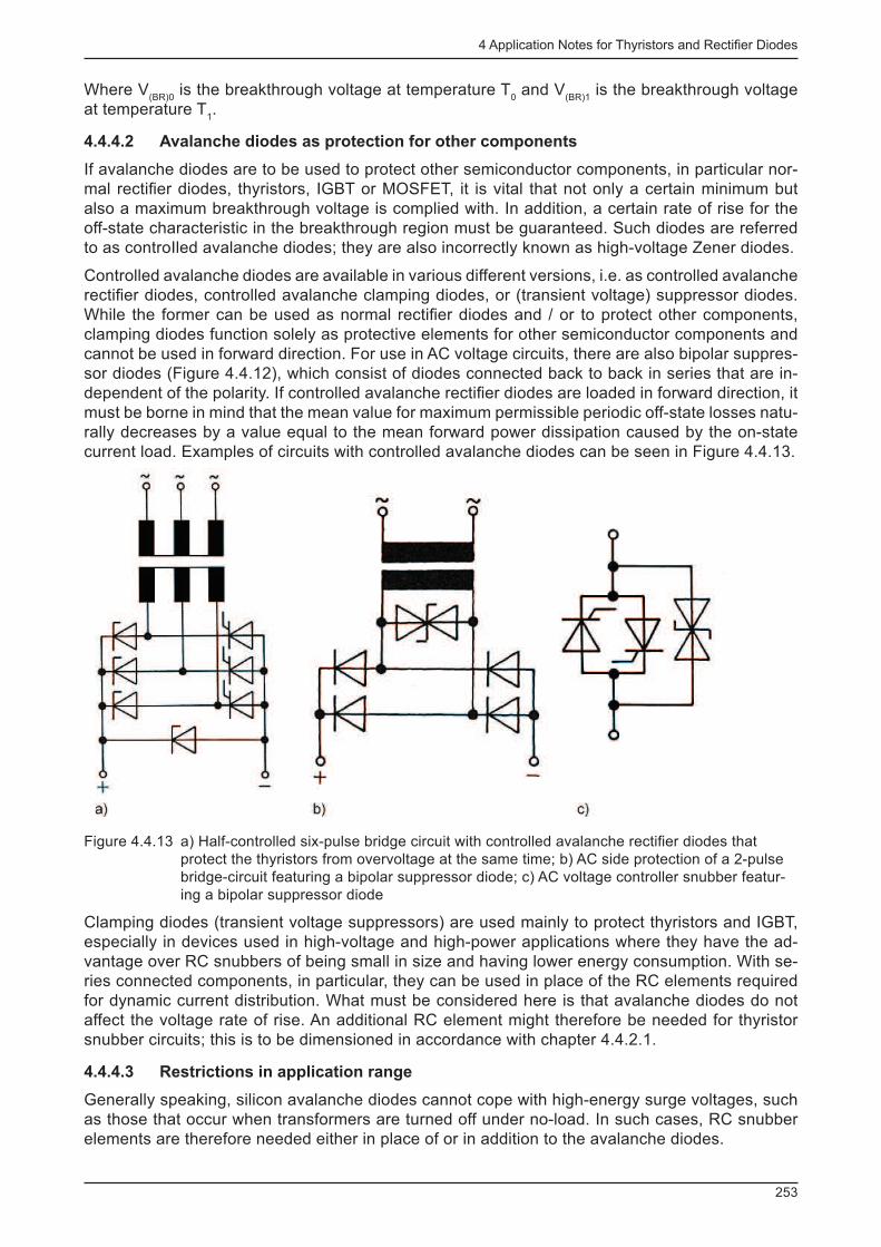
4 Application Notes for Thyristors and Rectifi er Diodes
253
Where V (BR)0
is the breakthrough voltage at temperature T 0 and V
(BR)1 is the breakthrough voltage
at temperature T 1 .
4.4.4.2 Avalanche diodes as protection for other components
If avalanche diodes are to be used to protect other semiconductor components, in particular nor-mal rectifi er diodes, thyristors, IGBT or MOSFET, it is vital that not only a certain minimum but also a maximum breakthrough voltage is complied with. In addition, a certain rate of rise for the off-state characteristic in the breakthrough region must be guaranteed. Such diodes are referred to as controIled avalanche diodes; they are also incorrectly known as high-voltage Zener diodes.
Controlled avalanche diodes are available in various different versions, i.e. as controlled avalanche rectifi er diodes, controlled avalanche clamping diodes, or (transient voltage) suppressor diodes. While the former can be used as normal rectifi er diodes and / or to protect other components, clamping diodes function solely as protective elements for other semiconductor components and cannot be used in forward direction. For use in AC voltage circuits, there are also bipolar suppres-sor diodes (Figure 4.4.12), which consist of diodes connected back to back in series that are in-dependent of the polarity. If controlled avalanche rectifi er diodes are loaded in forward direction, it must be borne in mind that the mean value for maximum permissible periodic off-state losses natu-rally decreases by a value equal to the mean forward power dissipation caused by the on-state current load. Examples of circuits with controlled avalanche diodes can be seen in Figure 4.4.13.
Figure 4.4.13 a) Half-controlled six-pulse bridge circuit with controlled avalanche rectifi er diodes that protect the thyristors from overvoltage at the same time; b) AC side protection of a 2-pulse bridge-circuit featuring a bipolar suppressor diode; c) AC voltage controller snubber featur-ing a bipolar suppressor diode
Clamping diodes (transient voltage suppressors) are used mainly to protect thyristors and IGBT, especially in devices used in high-voltage and high-power applications where they have the ad-vantage over RC snubbers of being small in size and having lower energy consumption. With se-ries connected components, in particular, they can be used in place of the RC elements required for dynamic current distribution. What must be considered here is that avalanche diodes do not affect the voltage rate of rise. An additional RC element might therefore be needed for thyristor snubber circuits; this is to be dimensioned in accordance with chapter 4.4.2.1.
4.4.4.3 Restrictions in application range
Generally speaking, silicon avalanche diodes cannot cope with high-energy surge voltages, such as those that occur when transformers are turned off under no-load. In such cases, RC snubber elements are therefore needed either in place of or in addition to the avalanche diodes.
4 Application Notes for Thyristors and Rectifi er Diodes
254
4.4.4.4 Case types
Small silicon avalanche diodes have cases with wire connections or are meant for soldering onto PCBs (SMD). Larger diodes feature standard cases with screw studs. They are also available as bridge circuits. Clamping diodes also come in symmetrical cases similar to fuses that contain two pn-junctions connected in series with opposite polarity. Such bipolar suppressor diodes have sym-metrical characteristics; one such diode is therefore suffi cient to protect a thyristor.
4.4.5 Overcurrent protection for diodes and thyristors
Here, the term overcurrent refers to a current load acting on the power semiconductor that, given the existing cooling conditions, would lead to the destruction of the component unless the current is turned off in time by means of suitable devices. Unlike a short-circuit, which is dealt with in the next chapter, this is not a current that rises steeply within a few milliseconds.
Such overload cannot be caused solely by an unforeseen current increase (overcurrent), it could also be caused by an unintentional change in cooling conditions. As a result, the component can-not cope with currents that are normally permissible when cooling is properly ensured. Examples of improper cooling are blocked fan slits, fan breakdown or, in water-cooled systems, malfunction in coolant supply. A number of well-established protective devices for overload conditions such as these are described below. Here, a differentiation must be made between protective devices which trigger as a result of unintentional current increase only and those which respond when the cool-ing system is not functioning properly, as well as devices which provide protection in both cases.
4.4.5.1 Devices for protection from overcurrents
Power circuit breakers
Power circuit breakers are the most common form of overload protection. There are switches with thermal, magnetic and thermo-magnetic tripping. Similar to fuses, their response times are dependent on the overcurrent and lie within the range of under 1 s; the response time for high overcurrent is shorter. Manufacturers show this ratio in the form of a characteristic that can be then compared with the overcurrent capability (current rating) of the semiconductor component. Note that the trip current of power circuit breakers and the currents in the current / time curves for safety fuses are always effective values, while the maximum surge current of the semiconductor components are peak values of sinusoidal half waves. Thus, if comparisons are to be made, these values fi rst have to be converted into effective values.
Throughout the entire possible time period, the trip current of the power circuit breaker has to be lower than the permissible overcurrent of the semiconductor component in the case of error. If this cannot be achieved for the entire period, an additional protective device - normally a semiconduc-tor fuse - has to be integrated for the period not covered.
Fuses
Fuses are intended fi rst and foremost to provide short-circuit protection (cf. chapter 4.4.6). In cer-tain circumstances, however, the fuse may also provide protection from overload in the aforemen-tioned sense of the word. To determine this, a comparison is to be made between the fuse current / time curve for the given period and the permissible overcurrents for the protected semiconductor component in the event of an error. It might be necessary to cover any remaining time in which the fuse in question does not provide protection with an additional protective device.
Suppression of driver signal
In controllable circuits, it makes sense to implement overcurrent protection by infl uencing the driver unit. When overcurrents occur that are not intended for operation, the trigger pulses are either fully suppressed, or the driver unit is designed such that the current is limited to a permissible level in any given conditions. The requirement for the use of the driver unit as protection is, of course, that the thyristor controllability is maintained long enough (i.e. the maximum permissible virtual junction temperature is not exceeded) for the driver protection to take effect. For short-circuit currents that rise steeply within one semi-oscillation, for example, protection via the driver unit is not possible.

4 Application Notes for Thyristors and Rectifi er Diodes
255
4.4.5.2 Protective devices for malfunctions in the cooling device
Wind vane relays
With enhanced air cooling, wind vane relays which trigger a protective component or infl uence the driver unit under error conditions can be used to protect the power semiconductors from overload should the fan break down or the fan vents be blocked.
Water fl ow monitors
In water-cooled systems, fl ow monitors or fl ow indicators can be used to monitor the coolant fl ow.
4.4.5.3 Devices that respond to both overcurrent and cooling unit malfunctions
The destruction of power semiconductors in overload conditions always happens due to exces-sive non-permissible temperatures, regardless of whether the overload results from overcurrent or malfunctions in the cooling unit. This is why it makes sense to use devices to protect the semicon-ductor devices that respond directly to this temperature increase.
Bimetal thermostats
Bimetal thermostats contain bimetal discs which, at a certain factory-set temperature, snap from one position to the next, opening or closing a contact in the process (Figure 4.4.14). They normally have screw studs with which they are screwed onto the heat sink, establishing the closest pos-sible thermal contact with the semiconductor components as possible. If several semiconductor components are to be protected by way of separate heat sinks, each of the heat sinks will in some cases require its own thermostat. The contacts are connected in series or parallel, depending on whether they open or close.
Bimetal thermostats can be used for natural or forced air cooling, as well as for water-cooled systems. In the latter case, it makes sense to use an additional thermostat which suppresses or completely blocks the coolant supply if a certain heat sink temperature is not reached. This will ensure that no condensation accumulates on the isolated parts of the semiconductor components.
Figure 4.4.14 Bimetal thermostat for screw-connection to a semiconductor heat sink; a) Design with open-ing contact in neutral position; b) Same design after the response temperature has been exceeded. The centre of the bimetal disc clicks upwards, opening the contact; c) Design with closing contact once the response temperature has been exceeded.
Temperature-dependent resistors
Temperature-dependent resistors have the advantage over bimetal thermostats that they respond to temperature changes more quickly, resulting in a minor safety margin between the operating current and the minimum current required to trip the protective device. An additional electronic circuit is needed to convert the change in resistance into a signal that can, for example, trigger a protective device.
Temperature-dependent resistors can also be integrated into power modules, for example sol-dered onto the insulating substrate. Integrated sensors such as these respond far more quickly than the sensors on the heat sink; having said that, these are defi nitely not enough to detect increases in chip temperature caused by steep overcurrents before chip damage occurs. The silicon-based resistors used have either a positive temperature coeffi cient (PTC) where the resist-
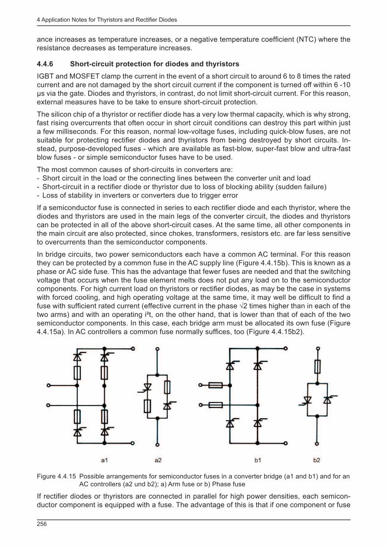
4 Application Notes for Thyristors and Rectifi er Diodes
256
ance increases as temperature increases, or a negative temperature coeffi cient (NTC) where the resistance decreases as temperature increases.
4.4.6 Short-circuit protection for diodes and thyristors
IGBT and MOSFET clamp the current in the event of a short circuit to around 6 to 8 times the rated current and are not damaged by the short circuit current if the component is turned off within 6 -10 µs via the gate. Diodes and thyristors, in contrast, do not limit short-circuit current. For this reason, external measures have to be take to ensure short-circuit protection.
The silicon chip of a thyristor or rectifi er diode has a very low thermal capacity, which is why strong, fast rising overcurrents that often occur in short circuit conditions can destroy this part within just a few milliseconds. For this reason, normal low-voltage fuses, including quick-blow fuses, are not suitable for protecting rectifi er diodes and thyristors from being destroyed by short circuits. In-stead, purpose-developed fuses - which are available as fast-blow, super-fast blow and ultra-fast blow fuses - or simple semiconductor fuses have to be used.
The most common causes of short-circuits in converters are: - Short circuit in the load or the connecting lines between the converter unit and load - Short-circuit in a rectifi er diode or thyristor due to loss of blocking ability (sudden failure) - Loss of stability in inverters or converters due to trigger error
If a semiconductor fuse is connected in series to each rectifi er diode and each thyristor, where the diodes and thyristors are used in the main legs of the converter circuit, the diodes and thyristors can be protected in all of the above short-circuit cases. At the same time, all other components in the main circuit are also protected, since chokes, transformers, resistors etc. are far less sensitive to overcurrents than the semiconductor components.
In bridge circuits, two power semiconductors each have a common AC terminal. For this reason they can be protected by a common fuse in the AC supply line (Figure 4.4.15b). This is known as a phase or AC side fuse. This has the advantage that fewer fuses are needed and that the switching voltage that occurs when the fuse element melts does not put any load on to the semiconductor components. For high current load on thyristors or rectifi er diodes, as may be the case in systems with forced cooling, and high operating voltage at the same time, it may well be diffi cult to fi nd a fuse with suffi cient rated current (effective current in the phase √2 times higher than in each of the two arms) and with an operating i²t, on the other hand, that is lower than that of each of the two semiconductor components. In this case, each bridge arm must be allocated its own fuse (Figure 4.4.15a). In AC controllers a common fuse normally suffi ces, too (Figure 4.4.15b2).
Figure 4.4.15 Possible arrangements for semiconductor fuses in a converter bridge (a1 and b1) and for an AC controllers (a2 und b2); a) Arm fuse or b) Phase fuse
If rectifi er diodes or thyristors are connected in parallel for high power densities, each semicon-ductor component is equipped with a fuse. The advantage of this is that if one component or fuse

4 Application Notes for Thyristors and Rectifi er Diodes
257
suddenly fails, the device will remain fully functional - with less power accordingly. The internal resistances of the fuses will also compensate somewhat for the differences in the characteristics of the semiconductor components, meaning the current distribution - in short-circuit conditions - will be more homogenous.
For short-circuit protection using blow-out fuses, short circuits are assumed to occur very seldom only. There are, however, applications where load short-circuit happens more frequently. In this case, a DC side high-speed circuit breaker, a power circuit breaker or another device to block the driver pulses of the thyristor (driver signal blocking) is needed on the load side. This has to be in addition to the fuses also needed because of the other short-circuit possibilities mentioned before. The converter circuit can, of course, be rated such that in the event of a load short circuit, until the switch responds, the overcurrent permissible for the semiconductor component cannot be exceed-ed. For driver signal blocking, the thyristor controllability must be ensured for the longest possible period of time up to the point of zero current crossing. Furthermore, the protective device on the load side has to be rated such that it responds faster than the thyristor or rectifi er diode blow-out fuses. This is referred to as selectivity.
4.4.6.1 Semiconductor fuses: terms and explanations
Fuse
Fuses are protective elements that melt a fuse element, in doing to opening the electric circuit if the current exceeds a given level during a given period of time.
Fuse mount
This is a fi xed integrated part of the fuse that contains the contact socket for the fuse link.
Fuse link
This part of the fuse contains the fusible element and has to be replaced after the fuse has been operational before it can function again (Figure 4.4.16). In semiconductor fuses, the fuse mount is often not needed. In this case, the fuse link and the fuse itself are identical.
Indicator
Device that shows the control state of the fuse link.
Figure 4.4.16 Cross-section of a semiconductor fuse link

4 Application Notes for Thyristors and Rectifi er Diodes
258
Fuse-link striker
This is released when the fusible element melts in order to activate a signal device or similar de-vice. This might double as the indicator. In circuits with parallel rectifi er diodes or thyristors, the response voltage of the fuse-link striker must be less than 1 V.
Rated voltage V N
Maximum permissible voltage with maximum 10% permissible short-time increase. If the rated voltage is an AC voltage, this will be specifi ed as an effective value. This applies to a sinusoidal voltage of 50 - 60 Hz. For non-sinusoidal voltage, neither the effective nor the crest value of the operating voltage may exceed the rated voltage or their sqrt(2) value√.
Rated current I N
Maximum permissible operating current with which the fuse mount may be continually subject to without changes that may be detrimental to function.
Rated breaking capacity I PM
Maximum prospective current that a fuse can turn off under certain conditions (e.g. recovery volt-age).
Let-through current (of a fuse) I (LT)
The maximum instantaneous current which is reached during fuse operation, if this turn-off pre-vents the prospective current from reaching its maximum value (Figure 4.4.17). Note that this value for current has nothing to do with the forward current of a rectifi er diode or thyristor!
Prospective current I P
Current which occurs if one imagines the fuse being replaced by an impedance-free conducting connection (dotted line in Figure 4.4.17).
Prospective short-circuit current I PS
Effective prospective current under short-circuit conditions directly behind the fuse. This value might be needed to determine the precise arcing i²t value.
Pre-arc time t pa
Time between the onset of a current that is large enough to melt the fusible element and the emer-gence of the arc (Figure 4.4.17).
Arcing time t a
Time that elapses between the generation of the arc and its (fi nal) extinction.
Operating time t op
Sum of the pre-arcing time and the arcing time.

4 Application Notes for Thyristors and Rectifi er Diodes
259
Figure 4.4.17 Current characteristic for short-circuit "turn-off" by a semiconductor fuse with current clamp-ing (let-through current smaller than the peak prospective current); Pre-arc time + arcing time = operating time
Time / current characteristic
Curve of the virtual pre-arc time or operating time as a function of the effective prospective current under certain conditions. This normally applies to 20°C initial temperature.
Pre-arc i²t value (i²t) pa
Integral of the square of the prospective current over pre-arc time:
dtI)t²i(pa
0
t
t
2
Ppa ò=
This depends on the initial temperature and the prospective short-circuit current. It is not time-dependent for pre-arc times of less than 10 ms.
Extinction i²t value (i²t) a
Integral of the square of the prospective current over arcing time:
dtI)t²i(a
pa
t
t
2
Pa ò=
This depends on the recovery voltage, the prospective current and the power factor.
Operating i²t value (i²t) op
Sum of the pre-arc i²t and the arcing i²t values.
Virtual time t vpa
, t va
, t vop
Resulting time if an i²t value is divided by the square of the prospective current, e.g.:
2
P
ava
I
)t²i(t =
In accordance with the various i²t values, virtual values for pre-arc time, arcing time (extinction time) and operating time are obtained.
4 Application Notes for Thyristors and Rectifi er Diodes
260
Switching voltage V aM
Peak voltage which occurs at the terminals of the fuse during fuse operation. This depends on the operating voltage and the power factor of the electric circuit. The quicker a fuse "clears", the higher the switching voltage.
Recovery voltage V WRMS
Voltage that occurs at the terminals of a fuse once the current has cut off.
Current limiting
Short-circuit current cut-off using a fuse, where the let-through current is smaller than the peak prospective short-circuit current (Example Figure 4.4.17). Whether current limiting takes place depends not only on the properties of the fuse but also on the amount of prospective short-circuit current I
PS , as well as on the operating frequency. For small I
PS , the pre-arc time is longer than a
quarter of an oscillation; likewise for operating frequencies greater than around 100 Hz. In this case, current limitation cannot happen.
4.4.6.2 Dimensioning semiconductor fuses
The following fuse-related data are to be borne in mind when dimensioning semiconductor fuses:
- Rated current - Rated voltage - Operating i²t value - Switching voltage
The infl uence of this data on the choice of suitable fuse is discussed in the following paragraphs in the order given above.
Dimensioning semiconductor fuses on the basis of the rated current
At rated current, a fuse link can be continually loaded under certain circumstances, i.e. at 20°C ambient temperature, unobstructed air convection and maximum 1.6 A/mm² current density in the connected lines. For higher ambient temperatures and smaller wire diameters, as commonly found in converter devices, the current is to be reduced. In almost every case, a reduction to 90% of the rated current level is enough. In enhanced air cooled systems, fuses may be subjected to currents that are greater than the rated current level. Some manufacturers give conversion equations or diagrams for this.
To check that the fuse is not subject to overload under the load and cooling conditions prevalent in the device, manufacturers recommend measuring the voltage for full load once exactly 5 seconds after turn-on (V
5s ) and once again 2 hours after turn-on (V
2h ); it goes without saying that this must
be done for exactly the same current. Owing to the temperature dependency of the fuse link resist-ance, these voltage values provide information on the temperature that the fuse link develops in application. The fuse is not overloaded if the following applies:
N14,1
T004,01
V
V a
h5
h2 £×+
×
Here, T a always the supply air temperature in °C and N is a constant of the relevant fuse which is
given by the manufacturer. This formula may differ slightly from one manufacturer to the next.
The rated current is the effective sinusoidal AC current. For non-sinusoidal current, as is usually the case in semiconductor fuses, the same effective value will normally be permissible. In cases where one is forced to fully utilise the rated current, even if the current is very different from the sine waveform, the manufacturer ought to be consulted.
Semiconductor fuses are used for rated currents of up to 630 A; in some, non-standard cases they are made for up to around 1600 A. For higher operating currents, two fuses have to be connected in parallel. In this case, either fuse mounts with low-tolerance fuse link resistances selected by the manufacturer are to be used or, for non-selected fuse mounts, a maximum of 80% rated current
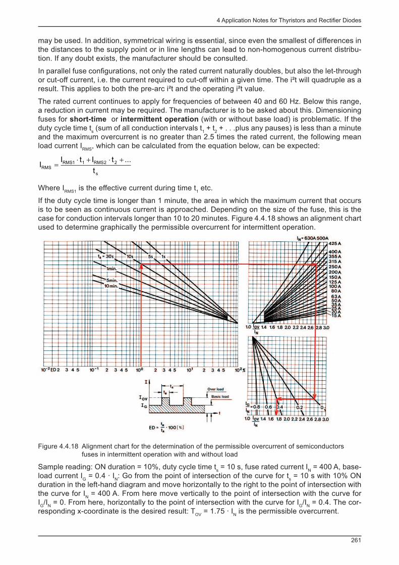
4 Application Notes for Thyristors and Rectifi er Diodes
261
may be used. In addition, symmetrical wiring is essential, since even the smallest of differences in the distances to the supply point or in line lengths can lead to non-homogenous current distribu-tion. If any doubt exists, the manufacturer should be consulted.
In parallel fuse confi gurations, not only the rated current naturally doubles, but also the let-through or cut-off current, i.e. the current required to cut-off within a given time. The i²t will quadruple as a result. This applies to both the pre-arc i²t and the operating i²t value.
The rated current continues to apply for frequencies of between 40 and 60 Hz. Below this range, a reduction in current may be required. The manufacturer is to be asked about this. Dimensioning fuses for short-time or intermittent operation (with or without base load) is problematic. If the duty cycle time t
s (sum of all conduction intervals t
1 + t
2 + . . .plus any pauses) is less than a minute
and the maximum overcurrent is no greater than 2.5 times the rated current, the following mean load current I
RMS , which can be calculated from the equation below, can be expected:
s
22RMS11RMSRMS
t
...tItII
+×+×=
Where I RMS1
is the effective current during time t 1 etc.
If the duty cycle time is longer than 1 minute, the area in which the maximum current that occurs is to be seen as continuous current is approached. Depending on the size of the fuse, this is the case for conduction intervals longer than 10 to 20 minutes. Figure 4.4.18 shows an alignment chart used to determine graphically the permissible overcurrent for intermittent operation.
Figure 4.4.18 Alignment chart for the determination of the permissible overcurrent of semiconductors fuses in intermittent operation with and without load
Sample reading: ON duration = 10%, duty cycle time t s = 10 s, fuse rated current I
N = 400 A, base-
load current I G = 0.4 · I
N : Go from the point of intersection of the curve for t
s = 10 s with 10% ON
duration in the left-hand diagram and move horizontally to the right to the point of intersection with the curve for I
N = 400 A. From here move vertically to the point of intersection with the curve for
I G /I
N = 0. From here, horizontally to the point of intersection with the curve for I
G /I
N = 0.4. The cor-
responding x-coordinate is the desired result: T OV
= 1.75 · I N is the permissible overcurrent.
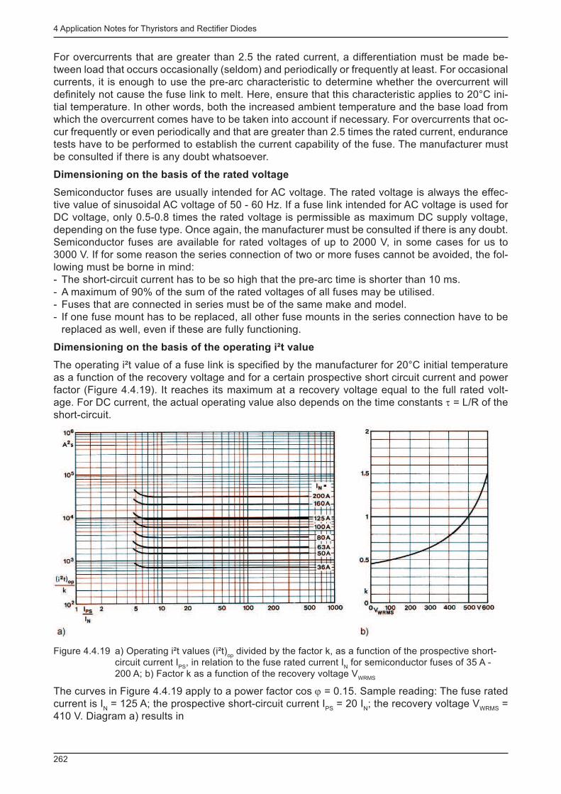
4 Application Notes for Thyristors and Rectifi er Diodes
262
For overcurrents that are greater than 2.5 the rated current, a differentiation must be made be-tween load that occurs occasionally (seldom) and periodically or frequently at least. For occasional currents, it is enough to use the pre-arc characteristic to determine whether the overcurrent will defi nitely not cause the fuse link to melt. Here, ensure that this characteristic applies to 20°C ini-tial temperature. In other words, both the increased ambient temperature and the base load from which the overcurrent comes have to be taken into account if necessary. For overcurrents that oc-cur frequently or even periodically and that are greater than 2.5 times the rated current, endurance tests have to be performed to establish the current capability of the fuse. The manufacturer must be consulted if there is any doubt whatsoever.
Dimensioning on the basis of the rated voltage
Semiconductor fuses are usually intended for AC voltage. The rated voltage is always the effec-tive value of sinusoidal AC voltage of 50 - 60 Hz. If a fuse link intended for AC voltage is used for DC voltage, only 0.5-0.8 times the rated voltage is permissible as maximum DC supply voltage, depending on the fuse type. Once again, the manufacturer must be consulted if there is any doubt. Semiconductor fuses are available for rated voltages of up to 2000 V, in some cases for us to 3000 V. If for some reason the series connection of two or more fuses cannot be avoided, the fol-lowing must be borne in mind: - The short-circuit current has to be so high that the pre-arc time is shorter than 10 ms. - A maximum of 90% of the sum of the rated voltages of all fuses may be utilised. - Fuses that are connected in series must be of the same make and model. - If one fuse mount has to be replaced, all other fuse mounts in the series connection have to be replaced as well, even if these are fully functioning.
Dimensioning on the basis of the operating i²t value
The operating i²t value of a fuse link is specifi ed by the manufacturer for 20°C initial temperature as a function of the recovery voltage and for a certain prospective short circuit current and power factor (Figure 4.4.19). It reaches its maximum at a recovery voltage equal to the full rated volt-age. For DC current, the actual operating value also depends on the time constants τ = L/R of the short-circuit.
Figure 4.4.19 a) Operating i²t values (i²t) op
divided by the factor k, as a function of the prospective short-circuit current I
PS , in relation to the fuse rated current I
N for semiconductor fuses of 35 A -
200 A; b) Factor k as a function of the recovery voltage V WRMS
The curves in Figure 4.4.19 apply to a power factor cos ϕ = 0.15. Sample reading: The fuse rated current is I
N = 125 A; the prospective short-circuit current I
PS = 20 I
N ; the recovery voltage V
WRMS =
410 V. Diagram a) results in

4 Application Notes for Thyristors and Rectifi er Diodes
263
sA101
k
)ti( 24OP
2
×=,
diagram b) results in k = 0.8. Therefore: (i²t) OP
= 0.8 · 10 4 A²s = 8000 A²s is the desired operating i²t value of the fuse.
Besides rated current and rated voltage, the operating i²t value is a critical parameter for selecting a semiconductor fuse. In the given conditions, this value must be smaller than the i²t value for the semiconductor component to be protected. Here, it is normally enough to compare the value for the "cold" fuse (initial temperature 20°C), as always specifi ed, with that of the "cold" semiconduc-tor component (virtual junction temperature T
j = 25°C), since the i²t value of the fuse decreases
more than that of the semiconductor component as the pre-load increases.
In the short-circuit region, i.e. at least ten times the rated current, semiconductor fuses have op-erating times of 5 - 10 ms. The i²t values for rectifi er diodes and thyristors apply for 8 - 10 ms. If the fuse operating time is below 8 ms, it is advisable to work on the basis of a 10 - 20% lower i²t value for the semiconductor component. The operating i²t value of the fuse, in contrast, is not time-dependent within this range of time. Furthermore, the strong dependence of the operating i²t value on the power factor of the given short-circuit electric circuit must be observed. Figure 4.4.20 shows a typical example. Short-circuit electric circuit in converter circuits often have power factors of around 0.3 - 0.35. For example, if the operating i²t value of the fuse applies to cos ϕ ≥ 0.2, virtu-ally every practical application is included.
Figure 4.4.20 Operating (i²t) value of a semiconductor fuse, in relation to the value for cos ϕ = 0.15, shown as a function of the power factor cos ϕ
As already mentioned, the operating i²t value is given as a function of the recovery voltage (Figure 4.4.19). It must be borne in mind that in converter circuits often two fuses are connected in series in the short-circuit circuit (Figure 4.4.21). In this case, the recovery voltage is only around half the value of the voltage driving the short circuit. Owing to voltage distribution which may be somewhat non-homogenous, it is advisable to use 60% of the voltage rating for each fuse.
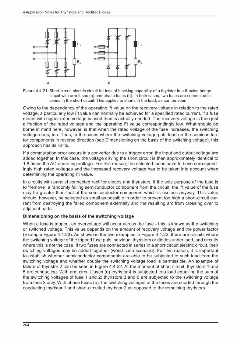
4 Application Notes for Thyristors and Rectifi er Diodes
264
Figure 4.4.21 Short-circuit electric circuit for loss of blocking capability of a thyristor in a 6-pulse bridge circuit with arm fuses (a) and phase fuses (b). In both cases, two fuses are connected in series in the short circuit. This applies to shorts in the load, as can be seen.
Owing to the dependency of the operating i²t value on the recovery voltage in relation to the rated voltage, a particularly low i²t value can normally be achieved for a specifi ed rated current, if a fuse mount with higher rated voltage is used than is actually needed. The recovery voltage is then just a fraction of the rated voltage and the operating i²t value correspondingly low. What should be borne in mind here, however, is that when the rated voltage of the fuse increases, the switching voltage does, too. Thus, in the cases where the switching voltage puts load on the semiconduc-tor components in reverse direction (see Dimensioning on the basis of the switching voltage), this approach has its limits.
If a commutation error occurs in a converter due to a trigger error, the input and output voltage are added together. In this case, the voltage driving the short circuit is then approximately identical to 1.8 times the AC operating voltage. For this reason, the selected fuses have to have correspond-ingly high rated voltages and the increased recovery voltage has to be taken into account when determining the operating i²t value.
In circuits with parallel connected rectifi er diodes and thyristors, if the sole purpose of the fuse is to "remove" a randomly failing semiconductor component from the circuit, the i²t value of the fuse may be greater than that of the semiconductor component which is useless anyway. This value should, however, be selected as small as possible in order to prevent too high a short-circuit cur-rent from destroying the failed component externally and the resulting arc from crossing over to adjacent parts.
Dimensioning on the basis of the switching voltage
When a fuse is tripped, an overvoltage will occur across the fuse - this is known as the switching or switched voltage. This value depends on the amount of recovery voltage and the power factor (Example Figure 4.4.23). As shown in the two examples in Figure 4.4.22, there are circuits where the switching voltage of the tripped fuse puts individual thyristors or diodes under load, and circuits where this is not the case. If two fuses are connected in series in a short-circuit electric circuit, their switching voltages may be added together (worst case scenario). For this reason, it is important to establish whether semiconductor components are able to be subjected to such load from the switching voltage and whether double the switching voltage load is permissible. An example of failure of thyristor 2 can be seen in Figure 4.4.22. At the moment of short circuit, thyristors 1 and 5 are conducting. With arm circuit fuses (a) thyristor 4 is subjected to a load equalling the sum of the switching voltages of fuse 1 and 2; thyristors 3 and 6 are subjected to the switching voltage from fuse 2 only. With phase fuses (b), the switching voltages of the fuses are shorted through the conducting thyristor 1 and short-circuited thyristor 2 as opposed to the remaining thyristors.
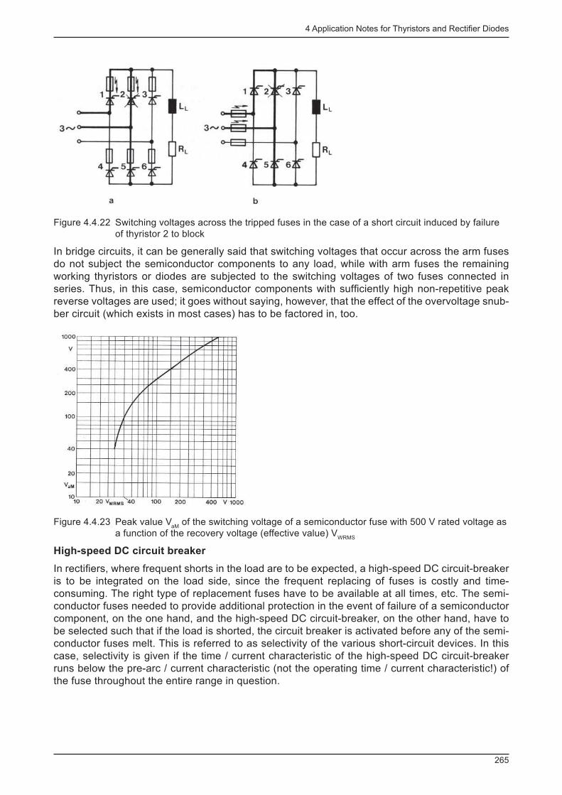
4 Application Notes for Thyristors and Rectifi er Diodes
265
Figure 4.4.22 Switching voltages across the tripped fuses in the case of a short circuit induced by failure of thyristor 2 to block
In bridge circuits, it can be generally said that switching voltages that occur across the arm fuses do not subject the semiconductor components to any load, while with arm fuses the remaining working thyristors or diodes are subjected to the switching voltages of two fuses connected in series. Thus, in this case, semiconductor components with suffi ciently high non-repetitive peak reverse voltages are used; it goes without saying, however, that the effect of the overvoltage snub-ber circuit (which exists in most cases) has to be factored in, too.
Figure 4.4.23 Peak value V aM
of the switching voltage of a semiconductor fuse with 500 V rated voltage as a function of the recovery voltage (effective value) V
WRMS
High-speed DC circuit breaker
In rectifi ers, where frequent shorts in the load are to be expected, a high-speed DC circuit-breaker is to be integrated on the load side, since the frequent replacing of fuses is costly and time-consuming. The right type of replacement fuses have to be available at all times, etc. The semi-conductor fuses needed to provide additional protection in the event of failure of a semiconductor component, on the one hand, and the high-speed DC circuit-breaker, on the other hand, have to be selected such that if the load is shorted, the circuit breaker is activated before any of the semi-conductor fuses melt. This is referred to as selectivity of the various short-circuit devices. In this case, selectivity is given if the time / current characteristic of the high-speed DC circuit-breaker runs below the pre-arc / current characteristic (not the operating time / current characteristic!) of the fuse throughout the entire range in question.
4 Application Notes for Thyristors and Rectifi er Diodes
266
4.5 Series and parallel connection of diodes and thyristors
4.5.1 Parallel connection of thyristors
In parallel thyristor circuit arrangements, homogenous current distribution is required from the mo-ment of fi ring and throughout the entire current fl ow time. For this purpose, steeply rising trigger pulses of suffi cient amplitude (see "Critical current rate of rise"), as well as symmetrical line im-pedances in the main circuit are needed. When connecting thyristors in parallel, it makes sense to arrange them by smallest possible forward voltage difference. To take into account any remaining asymmetry, we recommend operating the parallel thyristors with no more than 80 % of the calcu-lated maximum rated value for mean forward current. It may be necessary to limit the rate of rise of current in the individual thyristor using chokes.
4.5.2 Series connection of thyristors
To increase the off-state or blocking voltage, thyristors can be connected in series. Here, even voltage distribution must be ensured - using parallel resistors for blocking and off-state and using parallel RC elements for commutation (cf. chapter 4.4.2 Series connection). The parallel resistors have to be rated such that the current that fl ows through the resistors is is 5…10 times the thyris-tor off-state current in hot state. To ensure that the thyristor fi ring is as simultaneous as possible, suffi ciently high, steep-rising trigger pulses are required. The voltage load on each thyristor should be at least 10 % lower than for individual operation.
4.5.3 Parallel connection of rectifi er diodes
Parallel diode circuits must be as symmetrical as possible in order to achieve even current distri-bution in the electric circuit (connection point, wiring and wire length); this will rule out substantial differences in line impedances. It makes sense to arrange parallel diodes by the smallest possible difference in forward losses. To take into account any remaining asymmetry, we recommend op-erating the parallel rectifi er diodes with no more than 80% of the calculated maximum rated value for mean forward current.
4.5.4 Series connection of rectifi er diodes
To increase the blocking-state voltage, diodes may be connected in series. Especially when "many" diodes are connected in series, in most cases homogenous voltage distribution has to be forced: in blocking-state by using parallel resistors; during commutation using parallel RC elements (cf. chapter 4.4.2 Series connection). The parallel resistors have to be rated such that the current that fl ows through the resistors is 5…10 times the diode blocking-state current in hot state. These measures may not be necessary in series connected avalanche diodes. The voltage load on each diode should be at least 10% lower than for individual operation.

5 Application Notes for IGBT and MOSFET Modules
267
5 Application Notes for IGBT and MOSFET Modules
5.1 Selecting IGBT and MOSFET modules
The following sections will discuss some questions which are important for a successful selection of power modules containing IGBT or MOSFET. Corresponding information on diodes and thyris-tors was already included in the chapters 4.1 and 4.2. When selecting power modules for a specifi c application, the following factors must be taken into consideration: - voltage carrying capability, - current carrying capacity of transistors and freewheeling diodes under the feasible cooling condi-tions and in conjunction with the switching frequency,
- insulation requirements specifi ed by standards, such as insulation between module base plate and terminals and, if available, internal sensors (current, voltage, temperature),
in every stationary and short-time operating condition (e.g. overload). Under no static or dynamic condition may the stress lead to situations where the limits specifi ed for reverse recovery voltage, peak current, chip temperature and maximum rated operating point waveform in the datasheets are exceeded (cf. chapter 3.3.4 "SOA"). The same applies to the limits specifi ed for the module case (e.g insulation voltage, vibration strength, resistance to extreme climates, mounting instruc-tions). In the interest of reliability and suffi cient module lifetime, module utilisation must also factor in the intended number of load cycles where signifi cant temperature changes occur (cf. chapter 5.2 and 2.7).
As already detailed in the previous sections, many properties of power modules change in pro-portion to increases in temperature. Furthermore, dimensioning for "normal operating conditions" assumes that the semiconductor is not used up to the temperature limit T
j(max) . This is done in order
to keep a margin for overload conditions and to be able to revert to the static and dynamic charac-teristics guaranteed for T
j(max) - 25 K in the datasheets.
5.1.1 Operating voltage
5.1.1.1 Blocking voltage
Since most power modules are used in DC voltage links which are AC-voltage supplied via single-phase or three-phase rectifi er bridges, the blocking voltages of IGBT and MOSFET modules are adjusted to common line voltage levels for general-purpose use (600 V, 1200 V, 1700 V).
For this reason, a rough selection is fi rst made in the DC link from line voltage (control angle 0° for controlled rectifi ers) V
N or no-load direct voltage V
CC (V
DD ) as given in Table 5.1.1:
V N //V Rectifi cation V
CC ,V
DD /V V
DSS , V
CES /V
24 B2 22 50
48 B2 44 100
125 B2 110 200
200...246 B2 180...221 500, 600
400...480 B6 540...648 1200
575...690 B6 777...932 1700
Table 5.1.1 Line voltage levels, ideal no-load direct voltages and recommendations for the selection of IGBT or MOSFET modules
5 Application Notes for IGBT and MOSFET Modules
268
Afterwards, it is necessary to check whether under maximum voltage stress, i.e. - the rectifi ed value of the highest static input voltage (rated voltage + rated voltage tolerance) or output voltage of an active line rectifi er (cf. chapter 5.1.3) or PFC boost converter,
- transient line overvoltage, as far as it has not yet been reduced by line fi lters, DC link capacitors and circuits on the DC side (suppressor diodes, snubbers, varistors),
- DC link voltage peaks as a result of oscillations between the inductances and capacitances of the voltage supply, e.g. line fi lters, chokes, capacitors) under certain operating conditions,
- limiting voltage of a DC link chopper, if available; - turn-off overvoltage (example: IGBT) V
CC + ∆V with
∆V ≈ L σ · 0.8 I
max / t
f (I
Cmax )
where
L σ : Sum of all parasitic inductances in the commutation circuit
I max
: Highest collector current to be turned off
(mostly for active short-circuit turn-off)
t f (I
Cmax ): Fall time of collector current at ICmax
the blocking voltage is not exceeded.
In most datasheets, the limit values V CES
or V DSS
are given as limit values for the chip and not the module. The internal module inductance L
CE or L
DS (e.g. 20...30 nH), which is also specifi ed in
most datasheets, is part of L σ . Thus, the maximum voltage V
CEmax,T or V
DSmax,T present at the module
terminals must be limited, for example, to
V CEmax,T
≤ V CES
- L CE
· 0.8 I Cmax
/ t f (I
Cmax )
i.e. for the DC link voltage including every possible stationary or transient overvoltage, the follow-ing must be true, for example:
V CCmax
≤ V CES
- L σ · 0.8 I
Cmax / t
f (I
Cmax )
cf. chapters 3.3 and 3.4.
For IGBT modules, the voltage applied to the chips can be approximately verifi ed by performing measurements between the terminals C
x and E
x .
Such a measurement during active overcurrent / short-circuit switching – as demonstrated in Fig-ure 5.1.1 – shows that IGBT4 chips only permit the switching of relatively low overcurrents in the case of high DC link voltages (e.g. when braking, or feeding from a pulsed rectifi er / boost converter) and a low external gate resistance R
Goff , without V
CEmax being exceeded. To turn off an
IGBT4 in the event of a short circuit (e.g. when I C ≥ 2 · I
Cnom ), we therefore recommend a relatively
high R Goff
, e.g. > 20 Ω for a 300 A module, if the short-circuit current to be turned off is signifi cantly higher than the I
Cnom of the module; for details see chapter 3.3.1.
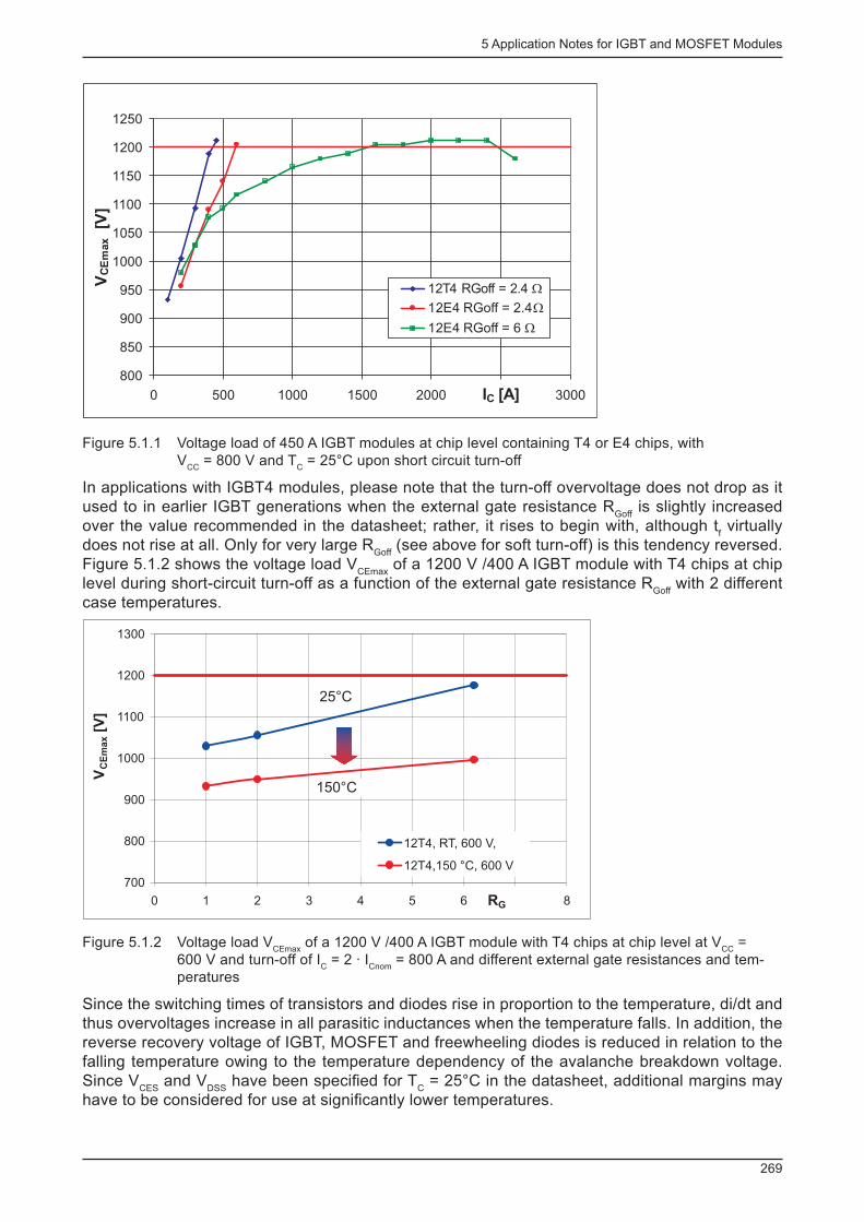
5 Application Notes for IGBT and MOSFET Modules
269
800
850
900
950
1000
1050
1100
1150
1200
1250
0 500 1000 1500 2000 2500 3000IC [A]
VC
Em
ax
[V]
12T4 RGoff = 2.4 W12E4 RGoff = 2.4W12E4 RGoff = 6 W
Figure 5.1.1 Voltage load of 450 A IGBT modules at chip level containing T4 or E4 chips, with V
CC = 800 V and T
C = 25°C upon short circuit turn-off
In applications with IGBT4 modules, please note that the turn-off overvoltage does not drop as it used to in earlier IGBT generations when the external gate resistance R
Goff is slightly increased
over the value recommended in the datasheet; rather, it rises to begin with, although t f virtually
does not rise at all. Only for very large R Goff
(see above for soft turn-off) is this tendency reversed. Figure 5.1.2 shows the voltage load V
CEmax of a 1200 V /400 A IGBT module with T4 chips at chip
level during short-circuit turn-off as a function of the external gate resistance R Goff
with 2 different case temperatures.
700
800
900
1000
1100
1200
1300
0 1 2 3 4 5 6 7 8RG
CE
max
[V]
12T4, RT, 600 V,
12T4,150 °C, 600 V
25°C
150°C
V
Figure 5.1.2 Voltage load V CEmax
of a 1200 V /400 A IGBT module with T4 chips at chip level at V CC
= 600 V and turn-off of I
C = 2 · I
Cnom = 800 A and different external gate resistances and tem-
peratures
Since the switching times of transistors and diodes rise in proportion to the temperature, di/dt and thus overvoltages increase in all parasitic inductances when the temperature falls. In addition, the reverse recovery voltage of IGBT, MOSFET and freewheeling diodes is reduced in relation to the falling temperature owing to the temperature dependency of the avalanche breakdown voltage. Since V
CES and V
DSS have been specifi ed for T
C = 25°C in the datasheet, additional margins may
have to be considered for use at signifi cantly lower temperatures.
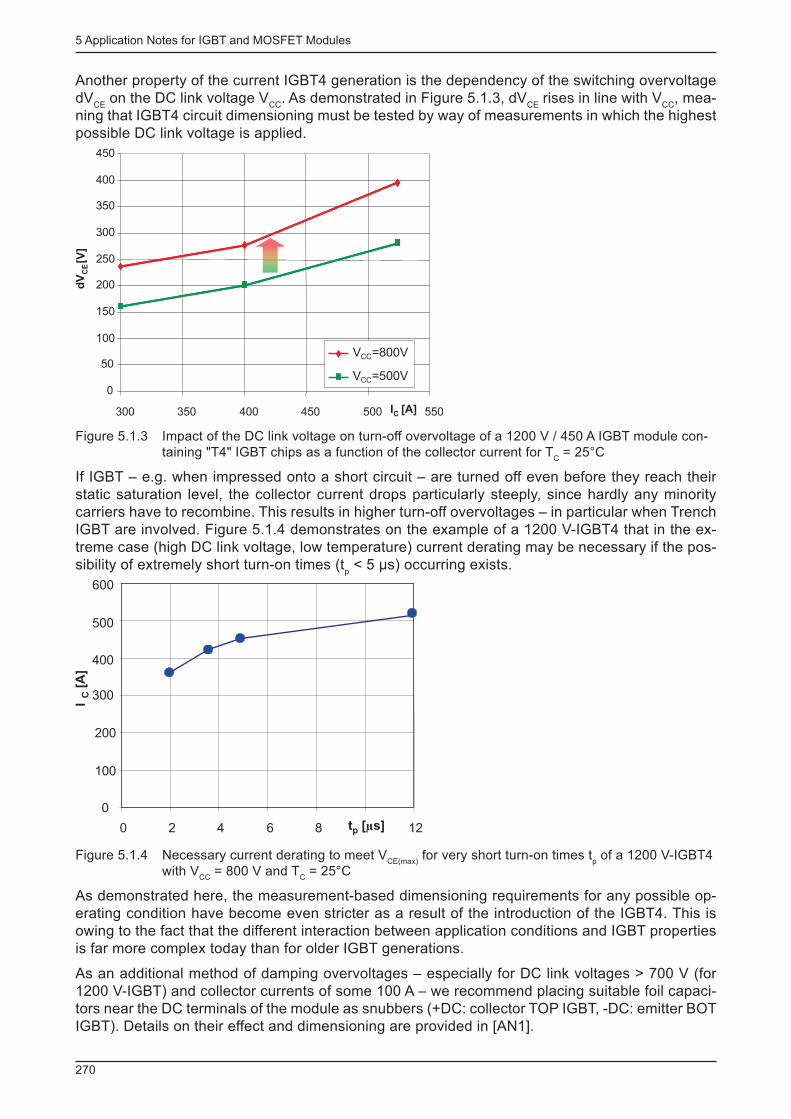
5 Application Notes for IGBT and MOSFET Modules
270
Another property of the current IGBT4 generation is the dependency of the switching overvoltage dV
CE on the DC link voltage V
CC . As demonstrated in Figure 5.1.3, dV
CE rises in line with V
CC , mea-
ning that IGBT4 circuit dimensioning must be tested by way of measurements in which the highest possible DC link voltage is applied.
0
50
100
150
200
250
300
350
400
450
300 350 400 450 500 550IC [A]
dV
CE[V
]
VCC=800V
VCC=500V
VCC=800V
VCC=500V
Figure 5.1.3 Impact of the DC link voltage on turn-off overvoltage of a 1200 V / 450 A IGBT module con-taining "T4" IGBT chips as a function of the collector current for T
C = 25°C
If IGBT – e.g. when impressed onto a short circuit – are turned off even before they reach their static saturation level, the collector current drops particularly steeply, since hardly any minority carriers have to recombine. This results in higher turn-off overvoltages – in particular when Trench IGBT are involved. Figure 5.1.4 demonstrates on the example of a 1200 V-IGBT4 that in the ex-treme case (high DC link voltage, low temperature) current derating may be necessary if the pos-sibility of extremely short turn-on times (t
p < 5 μs) occurring exists.
IC
[A]
0
100
200
300
400
500
0 2 4 6 8 12tp [ s]µ
600
Figure 5.1.4 Necessary current derating to meet V CE(max)
for very short turn-on times t p of a 1200 V-IGBT4
with V CC
= 800 V and T C = 25°C
As demonstrated here, the measurement-based dimensioning requirements for any possible op-erating condition have become even stricter as a result of the introduction of the IGBT4. This is owing to the fact that the different interaction between application conditions and IGBT properties is far more complex today than for older IGBT generations.
As an additional method of damping overvoltages – especially for DC link voltages > 700 V (for 1200 V-IGBT) and collector currents of some 100 A – we recommend placing suitable foil capaci-tors near the DC terminals of the module as snubbers (+DC: collector TOP IGBT, -DC: emitter BOT IGBT). Details on their effect and dimensioning are provided in [AN1].

5 Application Notes for IGBT and MOSFET Modules
271
5.1.1.2 Co-ordination of insulation
Co-ordination of insulation brings the voltage stress requirements for electrical insulation in line with the necessary withstand capability. Such co-ordination values, which have been obtained from past experience, have been laid down in standards and must be observed for equipment design.
For this purpose, a distinction is made between high-voltage (> 1000 V) and low-voltage systems (< 1000 V) to start with. For voltages < 1000 V, the (basic) standard EN 60664 (Insulation coor-dination for equipment within low-voltage systems) is the most crucial. The requirements of this standard are also refl ected in product group standards such as EN 50178 (Electronic equipment for use in power installations) or product standards such as EN 61800-5-1 (Adjustable speed electrical power drive systems - Safety requirements). Other standards, e.g. EN 50124-1 (Railway applications - Insulation coordination - Basic requirements), set down even more stringent require-ments for certain areas of application. The requirements derived from EN standards differ con-siderably from those set down in UL standards such as UL 508C (power conversion equipment).
For the purpose of insulation co-ordination, a distinction is made between three hierarchically graded requirements: - Functional insulation isolates different potentials within a circuit and takes purely functional, but no safety-relevant aspects into account.
- Basic insulation isolates mains supply circuits from earthed exposed parts and is thus vital for safety.
- Reinforced or double (= 2 x basic) insulation isolates mains supply circuits from unearthed ex-posed parts, on the one hand, and from information technology circuits, on the other hand. This means that no further protection is provided for equipment users, which is the reason why stricter requirements must be in place for insulation.
For power electronics components, such as power modules, this division means the following: - Functional insulation between the module terminals - Basic insulation between the module base plate (earthed in the device through the heatsink) and the module terminals
- Reinforced or double insulation between the module terminals and its insulated internal sensors (e.g. for current, voltage, temperature), whose outputs may be connected to the voltage potential of information electronics by the user without any additional measures being taken.
The user must already be aware of the electrical and environmental conditions (cf. chapter 6.2) to be expected when choosing a power module, i.e. at the beginning of the device design stage, since these conditions strongly infl uence insulation co-ordination.
For this reason, the following requirements must be analysed in addition to selecting the proper voltage class of IGBT or MOSFET in line with the highest peak voltage that will be encountered:
Mains overvoltage category in accordance with EN60664
- Assignment of voltage levels to areas of application, cf. Figure 5.1.5 - Standard: 3 for mains-connected circuits - Degree of pollution to which the power module is exposed in accordance with EN 60664 or EN 50178,
- depending on application conditions and the cooling concept of the device, for example - Standard: 2 if condensation is only possible in dead state, otherwise 3
Maximum altitude of application
- The dielectric strength of air is reduced in proportion to the altitude of installation (falling at-mospheric pressure) → reducing the insulation capability of clearances in air at the module, cf. chapter 6.2.6.
- Standard: up to 2000 m
5 Application Notes for IGBT and MOSFET Modules
272
Earthing of the supply network
- The earthing type of the supplying network determines the maximum voltage between earth po-tential and the connection terminals.
- Standard: neutral-earthed TN network
Maximum conductor-to-conductor voltage or highest DC supply voltage
- Is crucial for the selection of the relevant rated voltage - cf. Figure 5.1.5
Maximum DC link voltage
- It has to be factored in if the DC link voltage can exceed the rectifi ed mains voltage or DC sup-ply voltage, e.g. due to energy feedback, pulse rectifi er or inverter operation (e.g. 4Q inverter).
Insulation requirements for sensors and potential isolating spots for isolation from control
circuits
- Dependent on the requirements for the circuit to which the sensor is connected - If the sensor is connected to a mains circuit, functional insulation will be suffi cient. - If connected to a SELV or PELV circuit, the insulation between the load terminals of the module and the sensor must be "reinforced" or "doubled".
Maximum control voltage
- Maximum voltage of the control circuit against earth potential - Standard: < 50 V
Insulation requirements must be regarded separately for clearances in air, creepage distances and solid insulation. The clearances must be so large that fl ashover is prevented at all times. The determining factor for this is the highest peak voltage present. For this reason, particular consid-eration must be given to the overvoltage category of the circuit and its installation height. If this is > 2,000 m above mean sea level, the required clearance in air must be enlarged by an altitude correction factor, cf. Table 6.2.1 in chapter 6.2.6. For reinforced or double insulation, the clearance in air for the next voltage class up is required.
The degree of pollution and the resistance of the materials used with regard to surface currents determine the dimensioning of the creepage distances, which is described by the comparative tracking index (CTI). The more resistant a material is, the shorter the creepage distance may be. What is decisive here is the effective value of the voltage applied, not its peak value. Nevertheless, the creepage distance must be at least as large as the clearance in air. The minimum creepage distances required in standards were usually determined empirically, with only the tracking resist-ance of PCBs being determined for voltages of up to 1000 V and degrees of pollution 1 and 2 in experimental set-ups and the results adopted as a requirement. This is why the required distances here are much smaller than the CTI of the PCB material would actually require. To attain double or reinforced insulation, the creepage distance assigned to the voltage must be doubled.
Solid insulation is when the insulation distance is not created solely by air or gas. To verify that solid insulation withstands the voltage load, an impulse withstand and partial discharge test is performed. Ideally, the onsetting partial discharge voltage is greater than the maximum peak volt-age to be expected (because then partial discharge will never occur) and the intermittent partial discharge voltage is greater than the voltage continuously present. (If the maximum peak voltage is ever exceeded, the partial discharge which now starts must then be safely interrupted again). Some standards require a partial discharge test for reinforced or double insulation only.
In order to ensure that no fault has occurred during the assembly of the module or device, many product or product group standards require a dielectric test. This test does not serve the purpose of verifying that the insulation of the sample has been properly designed.

5 Application Notes for IGBT and MOSFET Modules
273
Figure 5.1.5 Insulation test voltages for selected network types, line voltages and overvoltage categories [54]
The above-mentioned standards provide different rating guidelines for the necessary insulation test voltages. Example: Insulation test voltages for basic insulation at a line voltage of 690 V for AC and DC testing according to different standards.
In accordance with EN 50178
Test duration: type test 5 s; routine test 1 s
a) earthed neutral
phase-earth voltage: 690 V/√3 = 398 V: V isol
= 398 V · 1.5 + 750 V = 1.35 kV rms
b) earthed delta circuit
phase-earth voltage: 690 V V isol
= 690 V · 1.5 + 750 V = 1.79 kV rms
In accordance with EN 61800-5-1
Test duration: type test 5 s; routine test 1 s
a) earthed neutral
phase-earth voltage: 690 V/√3 = 398 V V isol
= 398 V + 1200 V = 1.6 kV rms
b) earthed delta circuit
phase-earth voltage: 690 V V isol
= 690 V + 1200 V = 1.89 kV rms
In accordance with UL 508C
Test duration: 1 min
V isol
= 2 · V nominal
+ 1000 V V isol
= 2 · 690 V + 1000 V = 2.38 kV rms
The datasheets for power modules (see, for example, chapters 3.3.1 and 3.4.1, module limit val-ues) specify the insulation test voltage V
isol - which is tested by means of routine in-production
module testing - as the effective value (AC voltage, 50 Hz) between the input terminals / control terminals (all terminals connected) and the insulated module base plate. Test duration varies be-tween 1 s and 1 min. Alternatively, an insulation test can be performed as a DC test for V
isol( DC)=
√2 · V isol
(AC). Insulation testing for sensors contained in the module and their environment, as well as for isolation in intelligent modules is done in the same way.
5 Application Notes for IGBT and MOSFET Modules
274
In order to be able to use power modules across multiple applications, manufacturers specify test voltages as high as possible (within the scope of technical feasibility), for example 2.5 kVac/1 min…4 kVac/1 min….4.5 kVac/1 s for 1200 V-IGBT, 4 kVac/1 min…5.6 kV/1 s for 1700 V-IGBT, 6 kV/1 min for 3300 V-IGBT and 10.2 kV/1 min for 6500 V-IGBT. SEMIKRON also tests IGBT and diode modules at 9.5 kV/1 min in line with non-standard customer requirements.
All insulation voltage tests must be performed at an ambient temperature of 15…35°C, a relative humidity of 45…75% and an atmospheric pressure of 860…1060 hPa. The insulation test (dielec-tric test) is considered passed if no electrical breakdown has occurred, i.e. small leakage currents that occur are irrelevant. Since every insulation test may cause premature damage to the module as a result of partial discharge, the number of tests should be kept low and the test voltage should be no greater than necessary.
Insulation tests under the voltages specifi ed in the datasheets are not to be performed as part of inspections carried out on incoming shipments. Generally speaking, repetitive tests should be dis-pensed with. If they cannot be avoided, however, a regeneration time of at least 10 minutes must be complied with between 2 tests.
5.1.2 On-state current
The values specifi ed in the datasheets as maximum ratings I C
(collector DC), or I D (drain DC), at
which the maximum rated chip temperature is reached, are formally calculated for a stationary fully controlled transistor according to the following formula:
)cj(th)sat(CE
c(max)j
CRV
TTI
-×
-= (IGBT module)
)cj(th)on(DS
c(max)j
DRr
TTI
-×
-= (MOSFET module)
at case temperatures T c = 25°C and 80°C for modules with base plate, or T
s = 25°C and 70°C for
modules without base plate; also see the explanations given in the datasheet specifi cations in chapters 3.3.1 and 3.4. For modules without base plate, T
s substitutes T
c and R
th(j-s) substitutes
R th(j-c)
. Values for R DS(on)
and V CE(sat)
are those that apply at the maximum rated chip temperature T
j(max) . This information is intended for rough orientation only, since under real operating conditions
switching and (low) blocking losses will occur in addition to the forward on-state losses, the case temperature will differ and the static maximum ratings of R
DS(on) or V
CE(sat) will not be reached during
the entire turn-on process.
The IGBT chip current I Cnom
specifi ed in more recent datasheets is likewise intended for orienta-tion only (rated current of IGBT chips indicated in the chip manufacturer datasheet, multiplied by the number of chips connected in parallel in the module per switch) and is also a DC current (cf. chapter 3.4.1).
The repetitive peak collector current I CRM
is the maximum rated peak current value present at the collector terminal in pulsed operation, and thus the limit value for maximum current load during periodic switching operation (cf. chapter 3.3.1). I
CRM is not dependent on temperature and is limited
by the permissible chip current density. In many datasheets I CRM
is indicated as 2 · I Cnom
; this cor-responds to the former specifi ed limit for collector current I
CM . For IGBT4 chips (T4, E4) currently
used in SEMIKRON IGBT modules, the chip manufacturer specifi es I CRM
= 3 · I Cnom
, but without indicating a permissible pulse width. As shown in relevant tests, repetitive turn-off of such high currents may, however, cause early desaturation of the hottest chips and, consequently, involve high power losses. Therefore, SEMIKRON continues to recommend turning off currents above the permissible value specifi ed with 2 · I
Cnom within RBSOA as an exception only (e.g. DC link voltage
reduction, active clamping, very slow turn-off or turn-off snubber circuit) and retains the previous RBSOA limit of I
CRM = 2 · I
Cnom .
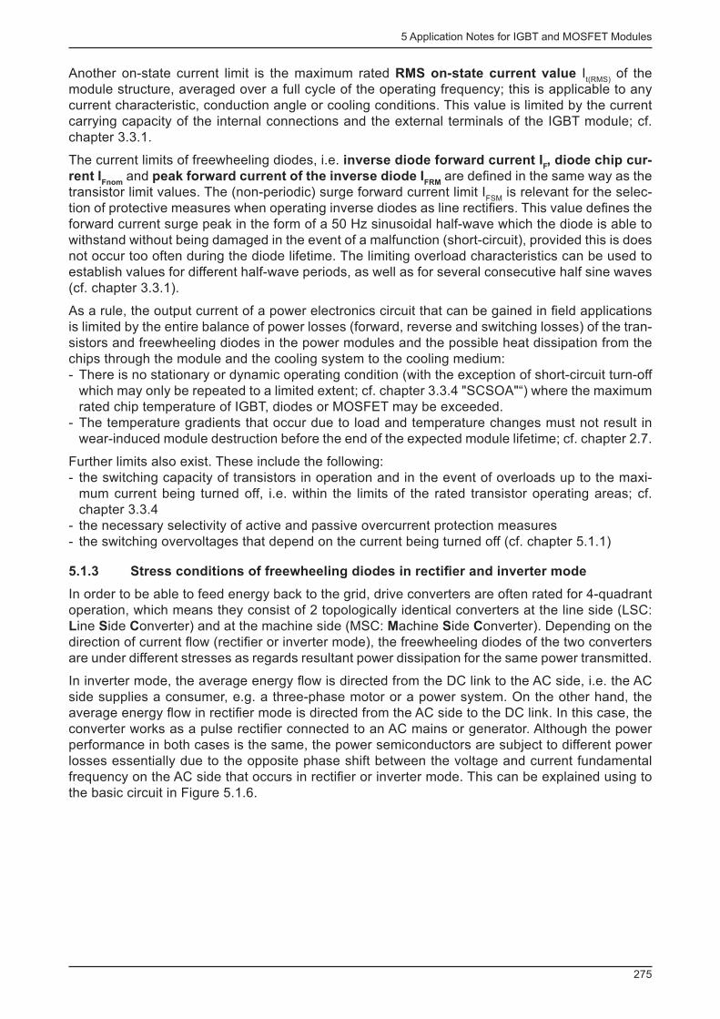
5 Application Notes for IGBT and MOSFET Modules
275
Another on-state current limit is the maximum rated RMS on-state current value I t(RMS)
of the module structure, averaged over a full cycle of the operating frequency; this is applicable to any current characteristic, conduction angle or cooling conditions. This value is limited by the current carrying capacity of the internal connections and the external terminals of the IGBT module; cf. chapter 3.3.1.
The current limits of freewheeling diodes, i.e. inverse diode forward current I F , diode chip cur-
rent I Fnom
and peak forward current of the inverse diode I FRM
are defi ned in the same way as the transistor limit values. The (non-periodic) surge forward current limit I
FSM is relevant for the selec-
tion of protective measures when operating inverse diodes as line rectifi ers. This value defi nes the forward current surge peak in the form of a 50 Hz sinusoidal half-wave which the diode is able to withstand without being damaged in the event of a malfunction (short-circuit), provided this is does not occur too often during the diode lifetime. The limiting overload characteristics can be used to establish values for different half-wave periods, as well as for several consecutive half sine waves (cf. chapter 3.3.1).
As a rule, the output current of a power electronics circuit that can be gained in fi eld applications is limited by the entire balance of power losses (forward, reverse and switching losses) of the tran-sistors and freewheeling diodes in the power modules and the possible heat dissipation from the chips through the module and the cooling system to the cooling medium: - There is no stationary or dynamic operating condition (with the exception of short-circuit turn-off which may only be repeated to a limited extent; cf. chapter 3.3.4 "SCSOA"“) where the maximum rated chip temperature of IGBT, diodes or MOSFET may be exceeded.
- The temperature gradients that occur due to load and temperature changes must not result in wear-induced module destruction before the end of the expected module lifetime; cf. chapter 2.7.
Further limits also exist. These include the following: - the switching capacity of transistors in operation and in the event of overloads up to the maxi-mum current being turned off, i.e. within the limits of the rated transistor operating areas; cf. chapter 3.3.4
- the necessary selectivity of active and passive overcurrent protection measures - the switching overvoltages that depend on the current being turned off (cf. chapter 5.1.1)
5.1.3 Stress conditions of freewheeling diodes in rectifi er and inverter mode
In order to be able to feed energy back to the grid, drive converters are often rated for 4-quadrant operation, which means they consist of 2 topologically identical converters at the line side (LSC: L ine S ide C onverter) and at the machine side (MSC: M achine S ide C onverter). Depending on the direction of current fl ow (rectifi er or inverter mode), the freewheeling diodes of the two converters are under different stresses as regards resultant power dissipation for the same power transmitted.
In inverter mode, the average energy fl ow is directed from the DC link to the AC side, i.e. the AC side supplies a consumer, e.g. a three-phase motor or a power system. On the other hand, the average energy fl ow in rectifi er mode is directed from the AC side to the DC link. In this case, the converter works as a pulse rectifi er connected to an AC mains or generator. Although the power performance in both cases is the same, the power semiconductors are subject to different power losses essentially due to the opposite phase shift between the voltage and current fundamental frequency on the AC side that occurs in rectifi er or inverter mode. This can be explained using to the basic circuit in Figure 5.1.6.
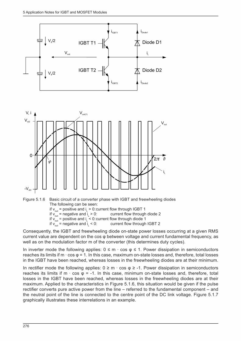
5 Application Notes for IGBT and MOSFET Modules
276
V /2d
V /2d
Vout
iIGBT1
iIGBT2 iDiode2
iL
Vd/2
V, i Vout(1)
Vout
iL
-Vd/2
IGBT T2
IGBT T1
Diode D2
Diode D1
iDiode1
Figure 5.1.6 Basic circuit of a converter phase with IGBT and freewheeling diodes The following can be seen: if v
out = positive and i
L > 0: current fl ow through IGBT 1
if v out
= negative and i L > 0: current fl ow through diode 2
if v out
= positive and i L < 0: current fl ow through diode 1
if v out
= negative and i L < 0: current fl ow through IGBT 2
Consequently, the IGBT and freewheeling diode on-state power losses occurring at a given RMS current value are dependent on the cos φ between voltage and current fundamental frequency, as well as on the modulation factor m of the converter (this determines duty cycles).
In inverter mode the following applies: 0 ≤ m · cos φ ≤ 1. Power dissipation in semiconductors reaches its limits if m · cos φ = 1. In this case, maximum on-state losses and, therefore, total losses in the IGBT have been reached, whereas losses in the freewheeling diodes are at their minimum.
In rectifi er mode the following applies: 0 ≥ m · cos φ ≥ -1. Power dissipation in semiconductors reaches its limits if m · cos φ = -1. In this case, minimum on-state losses and, therefore, total losses in the IGBT have been reached, whereas losses in the freewheeling diodes are at their maximum. Applied to the characteristics in Figure 5.1.6, this situation would be given if the pulse rectifi er converts pure active power from the line – referred to the fundamental component – and the neutral point of the line is connected to the centre point of the DC link voltage. Figure 5.1.7 graphically illustrates these interrelations in an example.
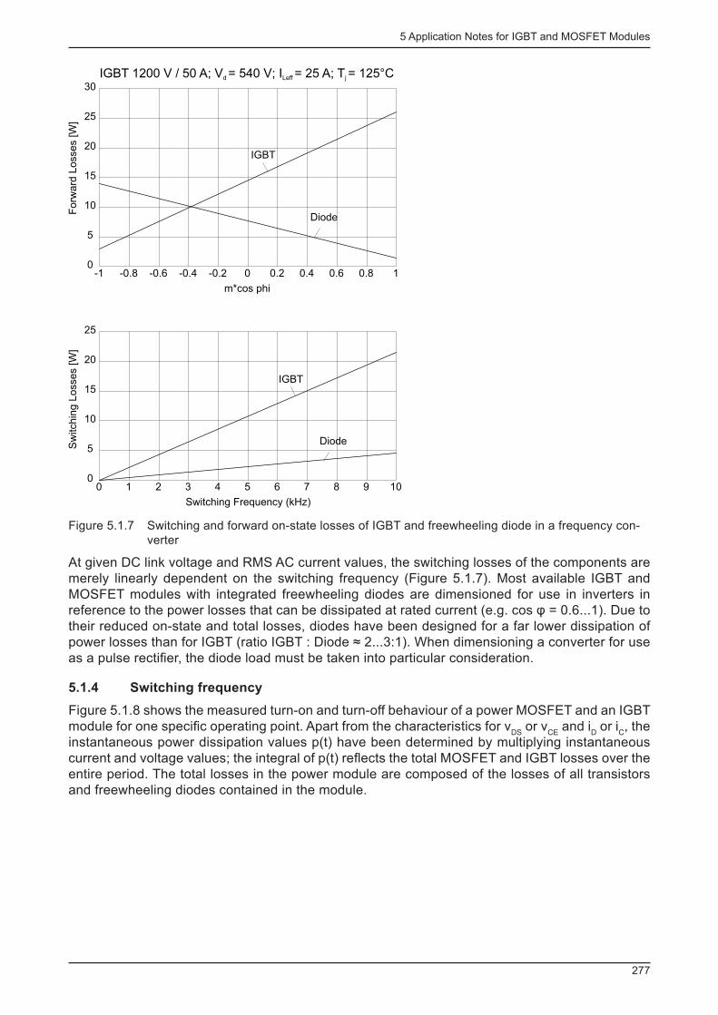
5 Application Notes for IGBT and MOSFET Modules
277
IGBT 1200 V / 50 A; V = 540 V; I = 25 A; T = 125°Cd Leff jF
orw
ard
Lo
sse
s [
W]
0
5
10
15
20
25
30
0-0.2-0.4-0.6-0.8-1 0.2 0.4 0.6 0.8 1
m*cos phi
543210 6 7 8 9 100
5
10
15
20
25
Sw
itchin
g L
osses [W
]
Switching Frequency (kHz)
IGBT
Diode
IGBT
Diode
Figure 5.1.7 Switching and forward on-state losses of IGBT and freewheeling diode in a frequency con-verter
At given DC link voltage and RMS AC current values, the switching losses of the components are merely linearly dependent on the switching frequency (Figure 5.1.7). Most available IGBT and MOSFET modules with integrated freewheeling diodes are dimensioned for use in inverters in reference to the power losses that can be dissipated at rated current (e.g. cos φ = 0.6...1). Due to their reduced on-state and total losses, diodes have been designed for a far lower dissipation of power losses than for IGBT (ratio IGBT : Diode ≈ 2...3:1). When dimensioning a converter for use as a pulse rectifi er, the diode load must be taken into particular consideration.
5.1.4 Switching frequency
Figure 5.1.8 shows the measured turn-on and turn-off behaviour of a power MOSFET and an IGBT module for one specifi c operating point. Apart from the characteristics for v
DS or v
CE and i
D or i
C , the
instantaneous power dissipation values p(t) have been determined by multiplying instantaneous current and voltage values; the integral of p(t) refl ects the total MOSFET and IGBT losses over the entire period. The total losses in the power module are composed of the losses of all transistors and freewheeling diodes contained in the module.
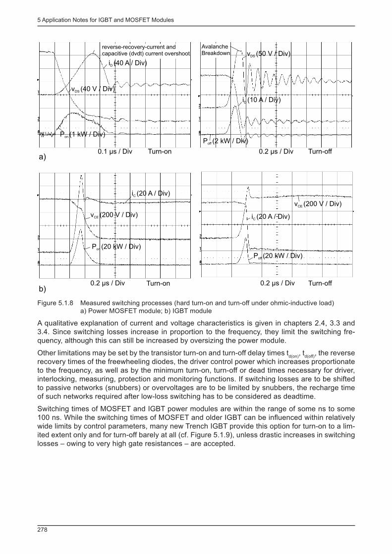
5 Application Notes for IGBT and MOSFET Modules
278
P (1 kW / Div)on
v (40 V / Div)DS
i (40 A / Div)D
reverse-recovery-current andcapacitive (dvdt) current overshoot
0.1 µs / Div Turn-on
i (10 A / Div)D
Turn-off0.2 µs / Div
P (2 kW / Div)off
v (50 V / Div)DS
AvalancheBreakdown
0.2 µs / Div Turn-on
v (200 V / Div)CE
P (20 kW / Div)on
i (20 A / Div)C
0.2 µs / Div Turn-off
v (200 V / Div)CE
i (20 A / Div)C
P (20 kW / Div)off
a)
b)
Figure 5.1.8 Measured switching processes (hard turn-on and turn-off under ohmic-inductive load) a) Power MOSFET module; b) IGBT module
A qualitative explanation of current and voltage characteristics is given in chapters 2.4, 3.3 and 3.4. Since switching losses increase in proportion to the frequency, they limit the switching fre-quency, although this can still be increased by oversizing the power module.
Other limitations may be set by the transistor turn-on and turn-off delay times t d(on)
, t d(off)
, the reverse recovery times of the freewheeling diodes, the driver control power which increases proportionate to the frequency, as well as by the minimum turn-on, turn-off or dead times necessary for driver, interlocking, measuring, protection and monitoring functions. If switching losses are to be shifted to passive networks (snubbers) or overvoltages are to be limited by snubbers, the recharge time of such networks required after low-loss switching has to be considered as deadtime.
Switching times of MOSFET and IGBT power modules are within the range of some ns to some 100 ns. While the switching times of MOSFET and older IGBT can be infl uenced within relatively wide limits by control parameters, many new Trench IGBT provide this option for turn-on to a lim-ited extent only and for turn-off barely at all (cf. Figure 5.1.9), unless drastic increases in switching losses – owing to very high gate resistances – are accepted.
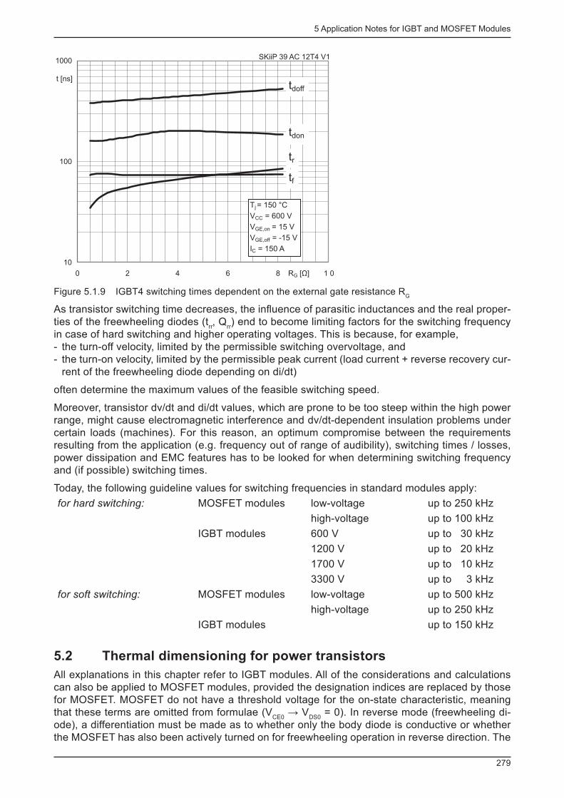
5 Application Notes for IGBT and MOSFET Modules
279
10
100
1000
0 2 4 6 8 1 0
tdon
tdoff
tr
tf
R [ ]G Ω
t [ns]
SKiiP 39 AC 12T4 V1
T = 150 °Cj
V = 600 VCC
V = 15 VGE,on
V = -15 VGE,off
I = 150 AC
Figure 5.1.9 IGBT4 switching times dependent on the external gate resistance R G
As transistor switching time decreases, the infl uence of parasitic inductances and the real proper-ties of the freewheeling diodes (t
rr , Q
rr ) end to become limiting factors for the switching frequency
in case of hard switching and higher operating voltages. This is because, for example, - the turn-off velocity, limited by the permissible switching overvoltage, and - the turn-on velocity, limited by the permissible peak current (load current + reverse recovery cur-rent of the freewheeling diode depending on di/dt)
often determine the maximum values of the feasible switching speed.
Moreover, transistor dv/dt and di/dt values, which are prone to be too steep within the high power range, might cause electromagnetic interference and dv/dt-dependent insulation problems under certain loads (machines). For this reason, an optimum compromise between the requirements resulting from the application (e.g. frequency out of range of audibility), switching times / losses, power dissipation and EMC features has to be looked for when determining switching frequency and (if possible) switching times.
Today, the following guideline values for switching frequencies in standard modules apply:
for hard switching: MOSFET modules low-voltage up to 250 kHz
high-voltage up to 100 kHz
IGBT modules 600 V up to 30 kHz
1200 V up to 20 kHz
1700 V up to 10 kHz
3300 V up to 3 kHz
for soft switching: MOSFET modules low-voltage up to 500 kHz
high-voltage up to 250 kHz
IGBT modules up to 150 kHz
5.2 Thermal dimensioning for power transistors
All explanations in this chapter refer to IGBT modules. All of the considerations and calculations can also be applied to MOSFET modules, provided the designation indices are replaced by those for MOSFET. MOSFET do not have a threshold voltage for the on-state characteristic, meaning that these terms are omitted from formulae (V
CE0 → V
DS0 = 0). In reverse mode (freewheeling di-
ode), a differentiation must be made as to whether only the body diode is conductive or whether the MOSFET has also been actively turned on for freewheeling operation in reverse direction. The
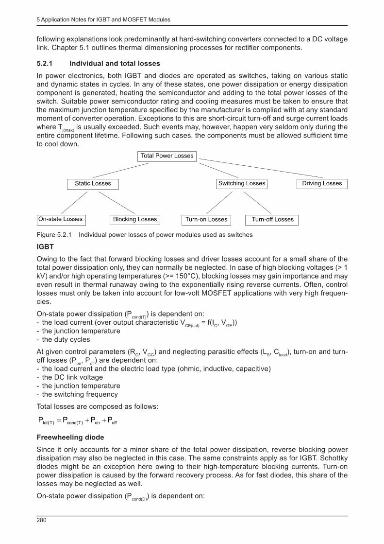
5 Application Notes for IGBT and MOSFET Modules
280
following explanations look predominantly at hard-switching converters connected to a DC voltage link. Chapter 5.1 outlines thermal dimensioning processes for rectifi er components.
5.2.1 Individual and total losses
In power electronics, both IGBT and diodes are operated as switches, taking on various static and dynamic states in cycles. In any of these states, one power dissipation or energy dissipation component is generated, heating the semiconductor and adding to the total power losses of the switch. Suitable power semiconductor rating and cooling measures must be taken to ensure that the maximum junction temperature specifi ed by the manufacturer is complied with at any standard moment of converter operation. Exceptions to this are short-circuit turn-off and surge current loads where T
j(max) is usually exceeded. Such events may, however, happen very seldom only during the
entire component lifetime. Following such cases, the components must be allowed suffi cient time to cool down.
Blocking Losses
Switching Losses
Total Power Losses
Static Losses
Turn-off LossesTurn-on Losses
Driving Losses
On-state Losses
Figure 5.2.1 Individual power losses of power modules used as switches
IGBT
Owing to the fact that forward blocking losses and driver losses account for a small share of the total power dissipation only, they can normally be neglected. In case of high blocking voltages (> 1 kV) and/or high operating temperatures (>= 150°C), blocking losses may gain importance and may even result in thermal runaway owing to the exponentially rising reverse currents. Often, control losses must only be taken into account for low-volt MOSFET applications with very high frequen-cies.
On-state power dissipation (P cond(T)
) is dependent on: - the load current (over output characteristic V
CE(sat) = f(I
C , V
GE ))
- the junction temperature - the duty cycles
At given control parameters (R G , V
GG ) and neglecting parasitic effects (L
S , C
load ), turn-on and turn-
off losses (P on
, P off
) are dependent on: - the load current and the electric load type (ohmic, inductive, capacitive) - the DC link voltage - the junction temperature - the switching frequency
Total losses are composed as follows:
offon)T(cond)T(tot PPPP ++=
Freewheeling diode
Since it only accounts for a minor share of the total power dissipation, reverse blocking power dissipation may also be neglected in this case. The same constraints apply as for IGBT. Schottky diodes might be an exception here owing to their high-temperature blocking currents. Turn-on power dissipation is caused by the forward recovery process. As for fast diodes, this share of the losses may be neglected as well.
On-state power dissipation (P cond(D)
) is dependent on:
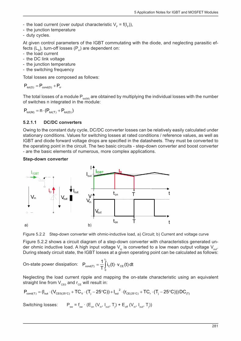
5 Application Notes for IGBT and MOSFET Modules
281
- the load current (over output characteristic V F = f(I
F )),
- the junction temperature - duty cycles.
At given control parameters of the IGBT commutating with the diode, and neglecting parasitic ef-fects (L
S ), turn-off losses (P
rr ) are dependent on:
- the load current - the DC link voltage - the junction temperature - the switching frequency
Total losses are composed as follows:
rr)D(cond)D(tot PPP +=
The total losses of a module P tot(M)
are obtained by multiplying the individual losses with the number of switches n integrated in the module:
)PP(nP )D(tot)T(tot)M(tot +×=
5.2.1.1 DC/DC converters
Owing to the constant duty cycle, DC/DC converter losses can be relatively easily calculated under stationary conditions. Values for switching losses at rated conditions / reference values, as well as IGBT and diode forward voltage drops are specifi ed in the datasheets. They must be converted to the operating point in the circuit. The two basic circuits - step-down converter and boost converter - are the basic elements of numerous, more complex applications.
Step-down converter
Figure 5.2.2 Step-down converter with ohmic-inductive load, a) Circuit; b) Current and voltage curve
Figure 5.2.2 shows a circuit diagram of a step-down converter with characteristics generated un-der ohmic inductive load. A high input voltage V
in is converted to a low mean output voltage V
out .
During steady circuit state, the IGBT losses at a given operating point can be calculated as follows:
On-state power dissipation: dt(t)v(t)iT
1P
1t
0
CECcond(T) ò ×=
Neglecting the load current ripple and mapping the on-state characteristic using an equivalent straight line from V
CE0 and r
CE will result in:
(T)jr)C25(CE
2
outjV)C25(0CEout)T(cond DC)))C25T(TCr(I))C25T(TCV(I(P °-×+×+°-×+×= °°
Switching losses: P sw
= f sw
· (E on
(V in , I
out , T
j ) + E
off (V
in , I
out , T
j ))
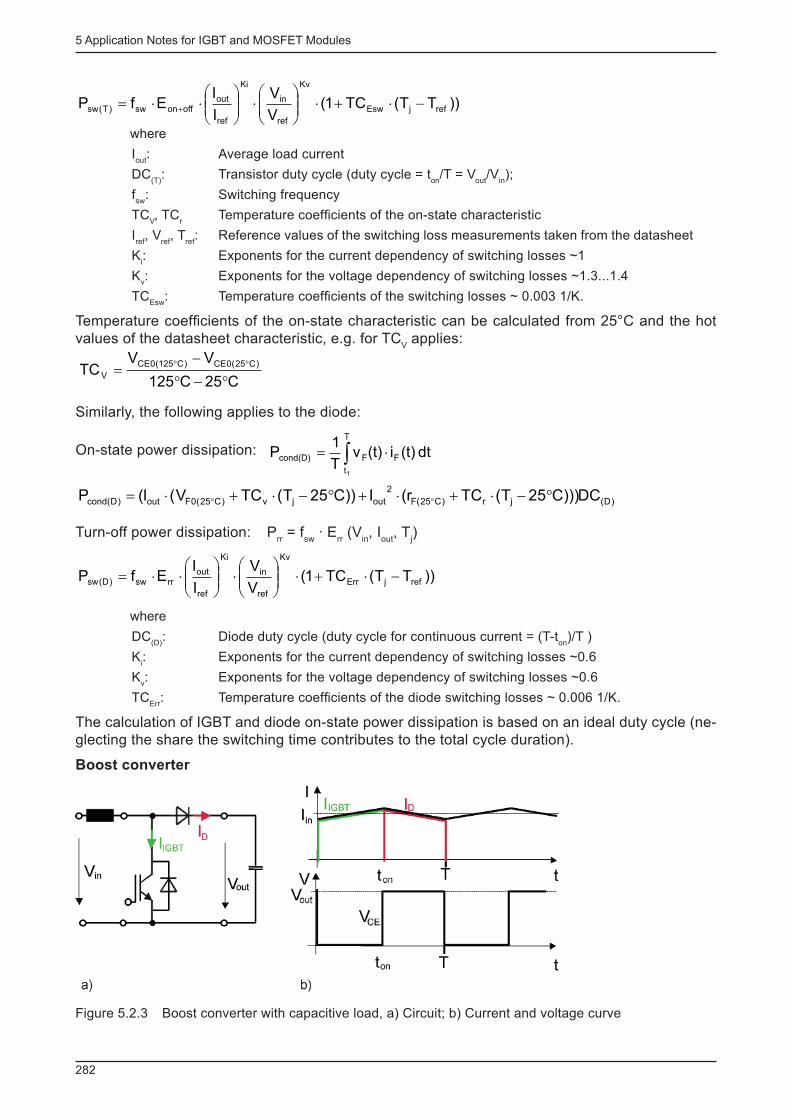
5 Application Notes for IGBT and MOSFET Modules
282
))TT(TC1(
V
V
I
IEfP refjEsw
Kv
ref
in
Ki
ref
outoffonsw)T(sw -×+×÷÷
ø
öççè
æ×÷÷
ø
öççè
æ××= +
where
I out
: Average load current
DC (T)
: Transistor duty cycle (duty cycle = t on
/T = V out
/V in );
f sw
: Switching frequency
TC V , TC
r Temperature coeffi cients of the on-state characteristic
I ref
, V ref
, T ref
: Reference values of the switching loss measurements taken from the datasheet
K i : Exponents for the current dependency of switching losses ~1
K v : Exponents for the voltage dependency of switching losses ~1.3...1.4
TC Esw
: Temperature coeffi cients of the switching losses ~ 0.003 1/K.
Temperature coeffi cients of the on-state characteristic can be calculated from 25°C and the hot values of the datasheet characteristic, e.g. for TC
V applies:
C25C125
VVTC
)C25(0CE)C125(0CE
V °-°
-= °°
Similarly, the following applies to the diode:
On-state power dissipation: dt(t)i(t)vT
1P
T
t
FFcond(D)
1
ò ×=
)D(jr)C25(F
2
outjv)C25(0Fout)D(cond DC)))C25T(TCr(I))C25T(TCV(I(P °-×+×+°-×+×= °°
Turn-off power dissipation: P rr = f
sw · E
rr (V
in , I
out , T
j )
))TT(TC1(V
V
I
IEfP refjErr
Kv
ref
in
Ki
ref
outrrsw)D(sw -×+×÷÷
ø
öççè
æ×÷÷
ø
öççè
æ××=
where
DC (D)
: Diode duty cycle (duty cycle for continuous current = (T-t on
)/T )
K i : Exponents for the current dependency of switching losses ~0.6
K v : Exponents for the voltage dependency of switching losses ~0.6
TC Err
: Temperature coeffi cients of the diode switching losses ~ 0.006 1/K.
The calculation of IGBT and diode on-state power dissipation is based on an ideal duty cycle (ne-glecting the share the switching time contributes to the total cycle duration).
Boost converter
Figure 5.2.3 Boost converter with capacitive load, a) Circuit; b) Current and voltage curve
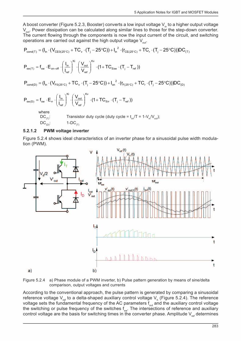
5 Application Notes for IGBT and MOSFET Modules
283
A boost converter (Figure 5.2.3, Booster) converts a low input voltage V in to a higher output voltage
V out
. Power dissipation can be calculated along similar lines to those for the step-down converter. The current fl owing through the components is now the input current of the circuit, and switching operations are carried out against the high output voltage V
out .
)T(jr)C25(CE
2
injv)C25(0CEin)T(cond DC)))C25T(TCr(I))C25T(TCV(I(P °-×+×+°-×+×= °°
))TT(TC1(V
V
I
IEfP refjEsw
Kv
ref
out
Ki
ref
inoffonsw)T(sw -×+×÷÷
ø
öççè
æ×÷÷
ø
öççè
æ××= +
)D(jr)C25(F
2
onjv)C25(0Fin)D(cond DC)))C25T(TCr(I))C25T(TCV(I(P °-×+×+°-×+×= °°
))TT(TC1(V
V
I
IEfP refjErr
Kv
ref
out
Ki
ref
inrrsw)D(sw -×+×÷÷
ø
öççè
æ×÷÷
ø
öççè
æ××=
where DC
(T) : Transistor duty cycle (duty cycle = t
on /T = 1-V
in /V
out );
DC (D)
: 1-DC (T)
5.2.1.2 PWM voltage inverter
Figure 5.2.4 shows ideal characteristics of an inverter phase for a sinusoidal pulse width modula-tion (PWM).
Figure 5.2.4 a) Phase module of a PWM inverter, b) Pulse pattern generation by means of sine/delta comparison, output voltages and currents
According to the conventional approach, the pulse pattern is generated by comparing a sinusoidal reference voltage V
ref to a delta-shaped auxiliary control voltage V
h (Figure 5.2.4). The reference
voltage sets the fundamental frequency of the AC parameters f out
and the auxiliary control voltage the switching or pulse frequency of the switches f
sw . The intersections of reference and auxiliary
control voltage are the basis for switching times in the converter phase. Amplitude V ref
determines
5 Application Notes for IGBT and MOSFET Modules
284
the voltage utilisation or the degree of converter modulation. Up to a ratio of V ref
= V h , this is called
linear modulation, where the modulation factor m <= 1. The modulation factor refers to the virtual neutral point of the load (phase-neutral) and a virtual centre point of the DC link voltage. It express-es the ratio between the fundamental amplitude of the AC voltage and 50% of the DC link voltage.
2
V
Vm
d
)1(out
)
=
)1(outV
)is the amplitude of the fundamental harmonic of the phase voltage to neutral
The phase shift between the fundamental harmonics of AC current and voltage is described by the angle ϕ. In inverter mode (energy fl ow from DC to AC) cos(ϕ) > 0 applies; in rectifi er mode (energy fl ow from AC to DC) cos(ϕ) < 0 applies, i.e. it is negative.
The current and voltage characteristics for IGBT and diodes will turn out to be identical yet time-shifted due to the symmetrical structure of the inverter circuit. It is therefore enough to consider just one IGBT and one diode with regard to loss evaluations. Inverter losses can then be deter-mined by multiplying the result by the corresponding number of IGBT/diodes (4 - single-phase or 6 - three-phase). In contrast to the calculations made in chapter 5.2.1.1, duty cycle, load current and junction temperature are not constant under static circuit conditions, but vary depending on the fundamental frequency of the AC side (e.g. 50/60 Hz). This means that the switching losses and on-state power dissipation of IGBT and diodes vary in time and call for a more in-depth analysis of system power losses. Precise results can thus only be expected insofar as the simplifi cations made are applicable, or deviations are still acceptable [55].
The following simplifi cations are assumed: - transistor and diode switching times are neglected - junction temperatures are temporally constant (permissible f
out = ~ 50 Hz)
- linear modulation - the switching frequency ripple of the AC current (sinusoidal current) is neglected - f
sw >> f
out
In a pure sine/delta comparison, the switching interlock time t d with f
sw · t
d *V
CC /2 at the voltage-time
area of the output voltage would be missing. An upstream regulator would balance the missing voltage by lengthening the control pulses, so that the voltage required to obtain the desired current value is also present at the inverter output. The calculation of the modulation factor m from the output voltage allows for t
d to be omitted as a source of error.
Conventional PWM will switch at the maximum number of possible commutation points in time, thus causing a maximum of switching losses. Other control methods, such as vector control, omit selected switching operations, thus showing lower switching losses than calculated using the for-mulae below. The linearisation of the IGBT output characteristic using an equivalent straight line results in the following expression for the temporal correlation of the saturation voltage v
CEsat :
tsinIrV(t)irV(t)v 1CECE0CCECE0CEsat w×+=×+=
Considering the sinusoidal dependency of duty cycles versus time, the on-state power dissipation of the IGBT may be calculated according to
2
1jCE1j0CE)T(cond Î)T(r3
)cos(m
8
1Î)T(V
8
)cos(m
2
1P ××÷
øö
çèæ
pj×
++××÷øö
çèæ j×
+p
=
Provided that the energy dissipation during switching is linearly dependent on the collector current, the total switching loss of an IGBT may be calculated with
5 Application Notes for IGBT and MOSFET Modules
285
( ))TT(TC1
V
V
I
I2EfP refjEsw
K
ref
cc
ref
outoffonsw)T(sw
V
-×+×÷÷ø
öççè
æ××
p××= +
where Î 1 : Amplitude of the inverter output current =1.41×I
out
V ce0
(T j ): Temperature-dependent threshold voltage of the on-state characteristic
r ce
(T j ): Temperature-dependent bulk resistance of the on-state characteristic
I ref
, V ref
, T ref
: Reference values of the switching loss measurements taken from the datasheet
K v : Exponents for the voltage dependency of switching losses ~1.3...1.4
TC Esw
: Temperature coeffi cients of the switching losses ~ 0.003 1/K.
This is actually based on the assumption that the IGBT switching losses generated during one sine half-wave of the current are approximately identical to the switching losses generated if an equiva-lent direct current is applied, which would correspond to the average value of the sine half-wave.
Accordingly, the following applies to the diode:
tsinirV(t)irV(t)v 1FF0FFF0F w×+=×+=
Considering the sinusoidal dependency of duty cycles versus time, the on-state power dissipation of diode D2 may be calculated according to
2
1jF1j0F)D(cond Î)T(r3
)cos(m
8
1Î)T(V
8
)cos(m
2
1P ××÷
øö
çèæ
pj×
-+××÷øö
çèæ j×
-p
=
Diode switching losses are approximated as follows:
( ))TT(TC1V
V
I
I2EfP refjErr
K
ref
cc
K
ref
1rrsw)D(sw
Vi
-+×÷÷ø
öççè
æ×÷
÷ø
öççè
æ×
p××=
V F0
(T j ): Temperature-dependent threshold voltage of the on-state characteristic
r F (T
j ): Temperature-dependent bulk resistance of the on-state characteristic
Kv: Exponents for the voltage dependency of switching losses ~0.6
K i : Exponents for the current dependency of switching losses ~0.6
TC Err
: Temperature coeffi cients of the switching losses ~ 0.006 1/K.
The formula for diode switching losses expresses an approximate only, since switching losses are not a linear function of the current (K
i ≠ 1). For this reason, the diode switching losses during a
sine half-wave are no longer identical to the switching losses of an equivalent direct current which corresponds to the average of the sine half-wave. The results rendered by the simplifi ed calcula-tion above are suffi cient for estimating the expected power dissipation during converter operation mode in practice. The decisive advantage that is offered to the user is that all necessary param-eters can be taken directly from the module datasheets.
5.2.2 Junction temperature calculation
5.2.2.1 Thermal equivalent circuit diagrams
The terms 'thermal resistance' and 'thermal impedance' have already been explained in chapter 2.5.2.2; this section deals with the types of modelling only. The calculation of junction temperatures is based on simplifi ed thermal equivalent circuit diagrams (Figure 5.2.5) in which three-dimension-al structures are mapped to one-dimensional models. This will inevitably result in errors, since thermal connections between different components inside one housing or on one heatsink are dependent on time as well as on the electric operating point of the components (e.g. distribution of losses between diode and IGBT). More complex models with a matrix composed of coupling ele-ments are impractical and diffi cult to parameterise [37]. If such effects have to be considered more closely, FEM simulations are preferred to the analytical approaches presented here.
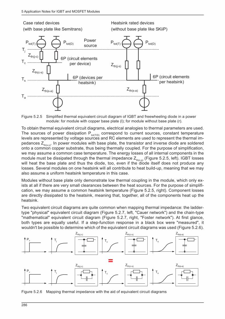
5 Application Notes for IGBT and MOSFET Modules
286
Case rated devices
(with base plate like Semitrans)
Heatsink rated devices
(without base plate like SKiiP)
6P (circuit elements
per device)
6P (devices per
heatsink)Ts
Tc
Tj
Zth(s-a)
Zth(c-s)
Zth(j-c)
Ta
Zth(s-a)
Zth(j-s)
6P (circuit elements
per heatsink)
Power
sourcePtot(T) Ptot(D) Ptot(T) Ptot(D)
Figure 5.2.5 Simplifi ed thermal equivalent circuit diagram of IGBT and freewheeling diode in a power module: for module with copper base plate (l); for module without base plate (r).
To obtain thermal equivalent circuit diagrams, electrical analogies to thermal parameters are used. The sources of power dissipation P
tot(T/D) correspond to current sources, constant temperature
levels are represented by voltage sources and RC elements are used to represent the thermal im-pedances Z
th(x-y) . In power modules with base plate, the transistor and inverse diode are soldered
onto a common copper substrate, thus being thermally coupled. For the purpose of simplifi cation, we may assume a common case temperature. The energy losses of all internal components in the module must be dissipated through the thermal impedance Z
th(c-s) (Figure 5.2.5, left). IGBT losses
will heat the base plate and thus the diode, too, even if the diode itself does not produce any losses. Several modules on one heatsink will all contribute to heat build-up, meaning that we may also assume a uniform heatsink temperature in this case.
Modules without base plate only demonstrate low thermal coupling in the module, which only ex-ists at all if there are very small clearances between the heat sources. For the purpose of simplifi -cation, we may assume a common heatsink temperature (Figure 5.2.5, right). Component losses are directly dissipated to the heatsink, meaning that, together, all of the components heat up the heatsink.
Two equivalent circuit diagrams are quite common when mapping thermal impedance: the ladder-type "physical" equivalent circuit diagram (Figure 5.2.7, left, "Cauer network") and the chain-type "mathematical" equivalent circuit diagram (Figure 5.2.7, right, "Foster network"). At fi rst glance, both types are equally useful. If a step-function response in a black box were "measured", it wouldn't be possible to determine which of the equivalent circuit diagrams was used (Figure 5.2.6).
Tj TcTs
Pv
=Tj
Pv TcTs
Zth(j-c) Zth(c-s)
Zth(c-s)Zth(j-c)
Zth(s-a)
Zth(s-a)
Figure 5.2.6 Mapping thermal impedance with the aid of equivalent circuit diagrams
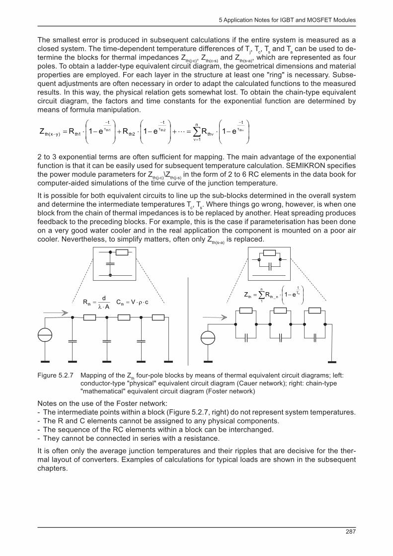
5 Application Notes for IGBT and MOSFET Modules
287
The smallest error is produced in subsequent calculations if the entire system is measured as a closed system. The time-dependent temperature differences of T
j , T
c , T
s and T
a can be used to de-
termine the blocks for thermal impedances Z th(j-c)
, Z th(c-s)
and Z th(s-a)
, which are represented as four poles. To obtain a ladder-type equivalent circuit diagram, the geometrical dimensions and material properties are employed. For each layer in the structure at least one "ring" is necessary. Subse-quent adjustments are often necessary in order to adapt the calculated functions to the measured results. In this way, the physical relation gets somewhat lost. To obtain the chain-type equivalent circuit diagram, the factors and time constants for the exponential function are determined by means of formula manipulation.
å=n
t
-
nt
-
t
-
- ÷÷
ø
ö
çç
è
æ-×=+
÷÷
ø
ö
çç
è
æ-×+
÷÷
ø
ö
çç
è
æ-×= n
n
1
t
th
t
2th
t
1th)yx(thth2th1th e1Re1Re1RZ L
2 to 3 exponential terms are often suffi cient for mapping. The main advantage of the exponential function is that it can be easily used for subsequent temperature calculation. SEMIKRON specifi es the power module parameters for Z
th(j-c) \Z
th(j-s) in the form of 2 to 6 RC elements in the data book for
computer-aided simulations of the time curve of the junction temperature.
It is possible for both equivalent circuits to line up the sub-blocks determined in the overall system and determine the intermediate temperatures T
c , T
s . Where things go wrong, however, is when one
block from the chain of thermal impedances is to be replaced by another. Heat spreading produces feedback to the preceding blocks. For example, this is the case if parameterisation has been done on a very good water cooler and in the real application the component is mounted on a poor air cooler. Nevertheless, to simplify matters, often only Z
th(s-a) is replaced.
cVCA
dR thth ×r×=
×l=
å ÷÷
ø
ö
çç
è
æ-×= T
n
1
t
n_ththne1RZ
Figure 5.2.7 Mapping of the Z th four-pole blocks by means of thermal equivalent circuit diagrams; left:
conductor-type "physical" equivalent circuit diagram (Cauer network); right: chain-type "mathematical" equivalent circuit diagram (Foster network)
Notes on the use of the Foster network: - The intermediate points within a block (Figure 5.2.7, right) do not represent system temperatures. - The R and C elements cannot be assigned to any physical components. - The sequence of the RC elements within a block can be interchanged. - They cannot be connected in series with a resistance.
It is often only the average junction temperatures and their ripples that are decisive for the ther-mal layout of converters. Examples of calculations for typical loads are shown in the subsequent chapters.
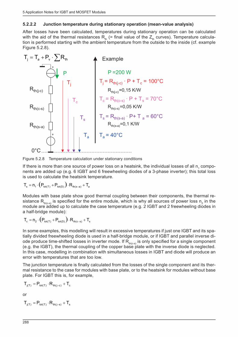
5 Application Notes for IGBT and MOSFET Modules
288
5.2.2.2 Junction temperature during stationary operation (mean-value analysis)
After losses have been calculated, temperatures during stationary operation can be calculated with the aid of the thermal resistances R
th (= fi nal value of the Z
th curves). Temperature calcula-
tion is performed starting with the ambient temperature from the outside to the inside (cf. example Figure 5.2.8).
0°C
Ta
Ts
Tc
Tj
Rth(j-c)
Rth(c-s)
Rth(s-a)
P P =200 W
Example
Ta = 40°C
Rth(j-c)=0,15 K/W
Rth(c-s)=0,05 K/W
Rth(s-a)=0,1 K/W
Ts = Rth(s-a) · P+ T a = 60°C
Tc = Rth(c-s) · P + Ts = 70°C
Tj = Rth(j-c) · P + Tc = 100°C
å×+= thvaj RPTT
Figure 5.2.8 Temperature calculation under stationary conditions
If there is more than one source of power loss on a heatsink, the individual losses of all n 1 compo-
nents are added up (e.g. 6 IGBT and 6 freewheeling diodes of a 3-phase inverter); this total loss is used to calculate the heatsink temperature.
( ) a)as(th)D(tot)T(tot1s TRPPnT +×+×= -
Modules with base plate show good thermal coupling between their components, the thermal re-sistance R
th(c-s) is specifi ed for the entire module, which is why all sources of power loss n
2 in the
module are added up to calculate the case temperature (e.g. 2 IGBT and 2 freewheeling diodes in a half-bridge module):
( ) s)sc(th)D(tot)T(tot2c TRPPnT +×+×= -
In some examples, this modelling will result in excessive temperatures if just one IGBT and its spa-tially divided freewheeling diode is used in a half-bridge module, or if IGBT and parallel inverse di-ode produce time-shifted losses in inverter mode. If R
th(c-s) is only specifi ed for a single component
(e.g. the IGBT), the thermal coupling of the copper base plate with the inverse diode is neglected. In this case, modelling in combination with simultaneous losses in IGBT and diode will produce an error with temperatures that are too low.
The junction temperature is fi nally calculated from the losses of the single component and its ther-mal resistance to the case for modules with base plate, or to the heatsink for modules without base plate. For IGBT this is, for example,
c)cj(th)T(tot)T(j TRPT +×= -
or
s)sj(th)T(tot)T(j TRPT +×= -
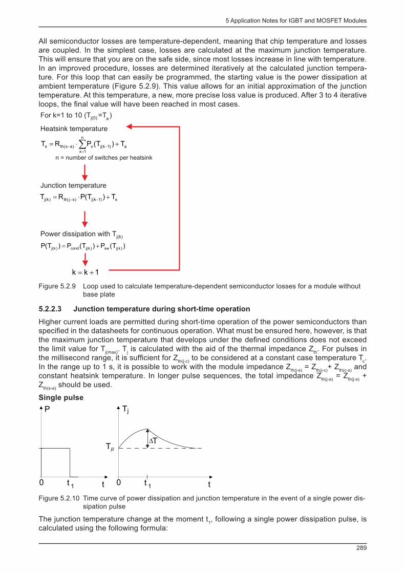
5 Application Notes for IGBT and MOSFET Modules
289
All semiconductor losses are temperature-dependent, meaning that chip temperature and losses are coupled. In the simplest case, losses are calculated at the maximum junction temperature. This will ensure that you are on the safe side, since most losses increase in line with temperature. In an improved procedure, losses are determined iteratively at the calculated junction tempera-ture. For this loop that can easily be programmed, the starting value is the power dissipation at ambient temperature (Figure 5.2.9). This value allows for an initial approximation of the junction temperature. At this temperature, a new, more precise loss value is produced. After 3 to 4 iterative loops, the fi nal value will have been reached in most cases.
1kk +=
)T(P)T(P)T(P )k(jsw)k(jcond)k(j +=
s)1k(j)sj(th)k(j T)T(PRT +×= --
å=
-- +×=n
1x
a)1k(jx)as(ths T)T(PRT
n = number of switches per heatsink
For k=1 to 10 (Tj(0) =Ta)
Heatsink temperature
Junction temperature
Power dissipation with Tj(k)
Figure 5.2.9 Loop used to calculate temperature-dependent semiconductor losses for a module without base plate
5.2.2.3 Junction temperature during short-time operation
Higher current loads are permitted during short-time operation of the power semiconductors than specifi ed in the datasheets for continuous operation. What must be ensured here, however, is that the maximum junction temperature that develops under the defi ned conditions does not exceed the limit value for T
j(max) . T
j is calculated with the aid of the thermal impedance Z
th . For pulses in
the millisecond range, it is suffi cient for Z th(j-c)
to be considered at a constant case temperature T c .
In the range up to 1 s, it is possible to work with the module impedance Z th(j-s)
= Z th(j-c)
+ Z th(c-s)
and constant heatsink temperature. In longer pulse sequences, the total impedance Z
th(j-a) = Z
th(j-s) +
Z th(s-a)
should be used.
Single pulse
P
tt0 t 10 t 1
Tj
T?Tj0
Figure 5.2.10 Time curve of power dissipation and junction temperature in the event of a single power dis-sipation pulse
The junction temperature change at the moment t 1 , following a single power dissipation pulse, is
calculated using the following formula:

5 Application Notes for IGBT and MOSFET Modules
290
å=n
tn ÷
÷
ø
ö
çç
è
æ××=D n
n
1
-t
thjth
1
e-1RPT
The following applies to the junction temperature curve during the cooling phase:
( ) åå=n
tn
=n
tn ÷
÷
ø
ö
çç
è
æ××
÷÷
ø
ö
çç
è
æ××=>D nn
n
1
)t--(t
th
n
1
-t
th1jth
1
th e-1RP-e-1RPttT
The formulae assume a fi xed reference temperature.
One-time sequence of m power dissipation pulses
P
t0
P1
T
t0 t 1 t 2 t 3
P2
P3
j
Tj0
Tj1 Tj2 Tj3? ? ?
Figure 5.2.11 Time curve of power dissipation and junction temperature in the event of a one-off sequence of m power dissipation pulses
The junction temperature change at the moment t 1 is to be calculated in the same way as for the
single pulse. For a junction temperature change at the moment t 2 , the following applies:
( ) åå=n
t
-
n=n
tn ÷
÷
ø
ö
çç
è
æ××-+
÷÷
ø
ö
çç
è
æ××=D nn
n
1
)t-(t
th12
n
1
-t
th12j e-1RPPe-1RP)t(T th
12
th
2
Junction temperature change at the moment t m :
( ) åå=n
tn
=mmm ÷
÷
ø
ö
çç
è
æ××-=D n
mn
1
)t--(t
th
m
1
1-mjth
1-m
e-1RPP)(tT
These formulae also assume a fi xed reference temperature. This formula enables the discretisa-tion of any time curve, meaning a time-dependent calculation of the temperature curve of complex load cycles can be programmed.
Junction temperature at constant pulse sequence
In order to calculate the mean and maximum junction temperature for periodically recurring power dissipation loads, the Z
th(j-c) curve of transistor and diode in periodic pulse operation can be used
as specifi ed in the datasheets.
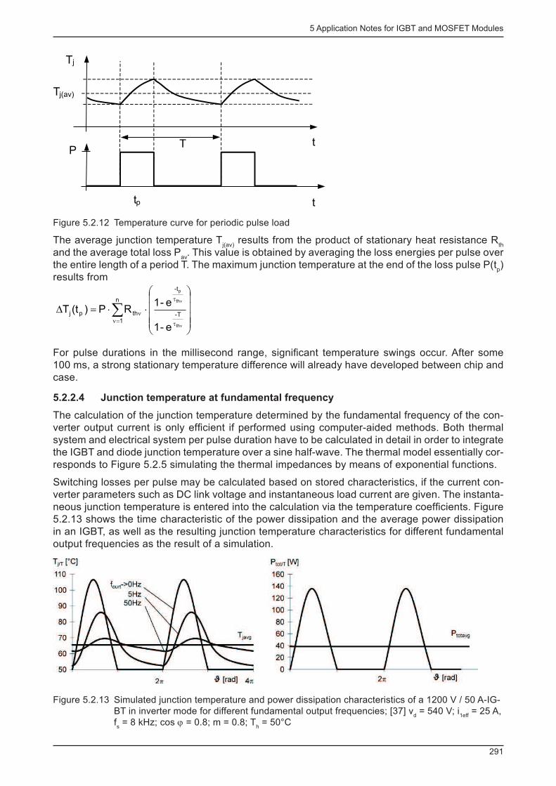
5 Application Notes for IGBT and MOSFET Modules
291
tp
T
t
Tj
Tj(av)
Pt
Figure 5.2.12 Temperature curve for periodic pulse load
The average junction temperature T j(av)
results from the product of stationary heat resistance R th
and the average total loss P av
. This value is obtained by averaging the loss energies per pulse over the entire length of a period T. The maximum junction temperature at the end of the loss pulse P(t
p )
results from
å=n t
t
n
÷÷÷÷
ø
ö
çççç
è
æ
××=Dn
nn
1T-
-t
thpj
th
th
p
e-1
e-1RP)(tT
For pulse durations in the millisecond range, signifi cant temperature swings occur. After some 100 ms, a strong stationary temperature difference will already have developed between chip and case.
5.2.2.4 Junction temperature at fundamental frequency
The calculation of the junction temperature determined by the fundamental frequency of the con-verter output current is only effi cient if performed using computer-aided methods. Both thermal system and electrical system per pulse duration have to be calculated in detail in order to integrate the IGBT and diode junction temperature over a sine half-wave. The thermal model essentially cor-responds to Figure 5.2.5 simulating the thermal impedances by means of exponential functions.
Switching losses per pulse may be calculated based on stored characteristics, if the current con-verter parameters such as DC link voltage and instantaneous load current are given. The instanta-neous junction temperature is entered into the calculation via the temperature coeffi cients. Figure 5.2.13 shows the time characteristic of the power dissipation and the average power dissipation in an IGBT, as well as the resulting junction temperature characteristics for different fundamental output frequencies as the result of a simulation.
Figure 5.2.13 Simulated junction temperature and power dissipation characteristics of a 1200 V / 50 A-IG-BT in inverter mode for different fundamental output frequencies; [37] v
d = 540 V; i
1eff = 25 A,
f s = 8 kHz; cos ϕ = 0.8; m = 0.8; T
h = 50°C
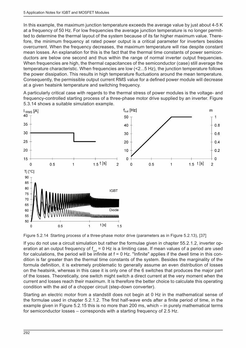
5 Application Notes for IGBT and MOSFET Modules
292
In this example, the maximum junction temperature exceeds the average value by just about 4-5 K at a frequency of 50 Hz. For low frequencies the average junction temperature is no longer permit-ted to determine the thermal layout of the system because of its far higher maximum value. There-fore, the minimum frequency at rated power output is a critical parameter for inverters besides overcurrent. When the frequency decreases, the maximum temperature will rise despite constant mean losses. An explanation for this is the fact that the thermal time constants of power semicon-ductors are below one second and thus within the range of normal inverter output frequencies. When frequencies are high, the thermal capacitances of the semiconductor (case) still average the temperature characteristic. When frequencies are low (<2...5 Hz), the junction temperature follows the power dissipation. This results in high temperature fl uctuations around the mean temperature. Consequently, the permissible output current RMS value for a defi ned power module will decrease at a given heatsink temperature and switching frequency.
A particularly critical case with regards to the thermal stress of power modules is the voltage- and frequency-controlled starting process of a three-phase motor drive supplied by an inverter. Figure 5.3.14 shows a suitable simulation example.
Figure 5.2.14 Starting process of a three-phase motor drive (parameters as in Figure 5.2.13), [37]
If you do not use a circuit simulation but rather the formulae given in chapter 55.2.1.2, inverter op-eration at an output frequency of f
out = 0 Hz is a limiting case. If mean values of a period are used
for calculations, the period will be infi nite at f = 0 Hz. "Infi nite" applies if the dwell time in this con-dition is far greater than the thermal time constants of the system. Besides the marginality of the formula defi nition, it is extremely problematic to generally assume an even distribution of losses on the heatsink, whereas in this case it is only one of the 6 switches that produces the major part of the losses. Theoretically, one switch might switch a direct current at the very moment when the current and losses reach their maximum. It is therefore the better choice to calculate this operating condition with the aid of a chopper circuit (step-down converter).
Starting an electric motor from a standstill does not begin at 0 Hz in the mathematical sense of the formulae used in chapter 5.2.1.2. The fi rst half-wave ends after a fi nite period of time, in the example given in Figure 5.2.15 this is no more than 200 ms, which – in purely mathematical terms for semiconductor losses – corresponds with a starting frequency of 2.5 Hz.
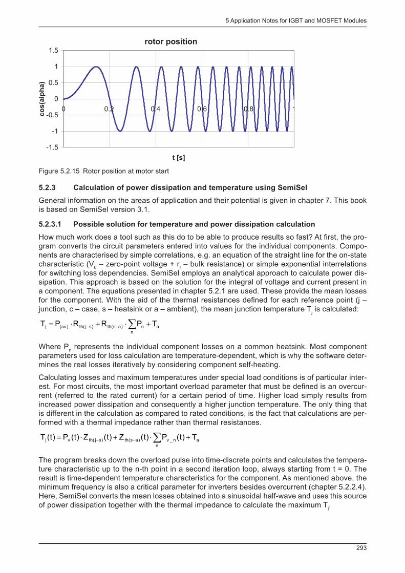
5 Application Notes for IGBT and MOSFET Modules
293
rotor position
-1.5
-1
-0.5
0
0.5
1
1.5
0 0.2 0.4 0.6 0.8 1
t [s]
co
s(a
lph
a)
Figure 5.2.15 Rotor position at motor start
5.2.3 Calculation of power dissipation and temperature using SemiSel
General information on the areas of application and their potential is given in chapter 7. This book is based on SemiSel version 3.1.
5.2.3.1 Possible solution for temperature and power dissipation calculation
How much work does a tool such as this do to be able to produce results so fast? At fi rst, the pro-gram converts the circuit parameters entered into values for the individual components. Compo-nents are characterised by simple correlations, e.g. an equation of the straight line for the on-state characteristic (V
0 – zero-point voltage + r
f – bulk resistance) or simple exponential interrelations
for switching loss dependencies. SemiSel employs an analytical approach to calculate power dis-sipation. This approach is based on the solution for the integral of voltage and current present in a component. The equations presented in chapter 5.2.1 are used. These provide the mean losses for the component. With the aid of the thermal resistances defi ned for each reference point (j – junction, c – case, s – heatsink or a – ambient), the mean junction temperature T
j is calculated:
a
n
n)as(th)sj(th)av(j TPRRPT +×+×= å--
Where P n represents the individual component losses on a common heatsink. Most component
parameters used for loss calculation are temperature-dependent, which is why the software deter-mines the real losses iteratively by considering component self-heating.
Calculating losses and maximum temperatures under special load conditions is of particular inter-est. For most circuits, the most important overload parameter that must be defi ned is an overcur-rent (referred to the rated current) for a certain period of time. Higher load simply results from increased power dissipation and consequently a higher junction temperature. The only thing that is different in the calculation as compared to rated conditions, is the fact that calculations are per-formed with a thermal impedance rather than thermal resistances.
a
n
n_v)as(th)sj(thvj T)t(P)t(Z)t(Z)t(P)t(T +×+×= å--
The program breaks down the overload pulse into time-discrete points and calculates the tempera-ture characteristic up to the n-th point in a second iteration loop, always starting from t = 0. The result is time-dependent temperature characteristics for the component. As mentioned above, the minimum frequency is also a critical parameter for inverters besides overcurrent (chapter 5.2.2.4). Here, SemiSel converts the mean losses obtained into a sinusoidal half-wave and uses this source of power dissipation together with the thermal impedance to calculate the maximum T
j .
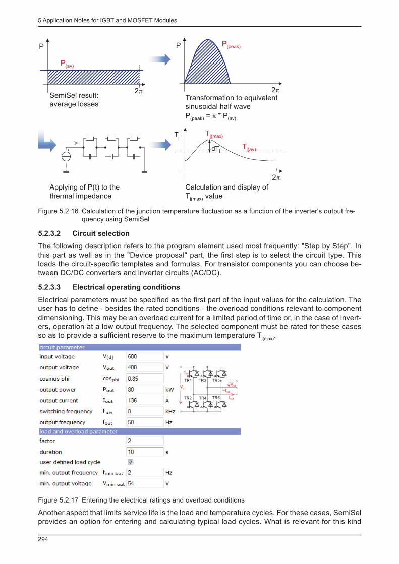
5 Application Notes for IGBT and MOSFET Modules
294
2p
P
2p
P
SemiSel result:
average lossesTransformation to equivalent
sinusoidal half wave
P(peak) = p * P(av)
P(peak)
P(av)
Applying of P(t) to the
thermal impedance
Tj
Tj(av)dTj
Tj(max)
2pCalculation and display of
Tj(max) value
Figure 5.2.16 Calculation of the junction temperature fl uctuation as a function of the inverter's output fre-quency using SemiSel
5.2.3.2 Circuit selection
The following description refers to the program element used most frequently: "Step by Step". In this part as well as in the "Device proposal" part, the fi rst step is to select the circuit type. This loads the circuit-specifi c templates and formulas. For transistor components you can choose be-tween DC/DC converters and inverter circuits (AC/DC).
5.2.3.3 Electrical operating conditions
Electrical parameters must be specifi ed as the fi rst part of the input values for the calculation. The user has to defi ne - besides the rated conditions - the overload conditions relevant to component dimensioning. This may be an overload current for a limited period of time or, in the case of invert-ers, operation at a low output frequency. The selected component must be rated for these cases so as to provide a suffi cient reserve to the maximum temperature T
j(max) .
Figure 5.2.17 Entering the electrical ratings and overload conditions
Another aspect that limits service life is the load and temperature cycles. For these cases, SemiSel provides an option for entering and calculating typical load cycles. What is relevant for this kind
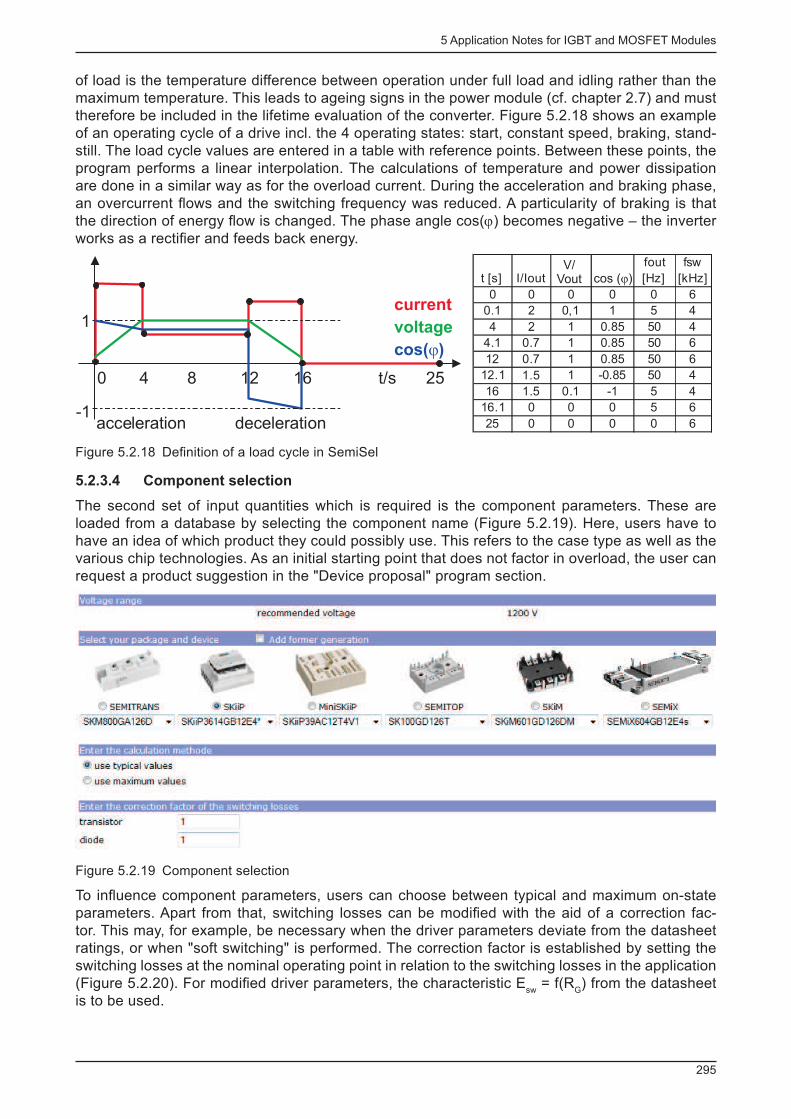
5 Application Notes for IGBT and MOSFET Modules
295
of load is the temperature difference between operation under full load and idling rather than the maximum temperature. This leads to ageing signs in the power module (cf. chapter 2.7) and must therefore be included in the lifetime evaluation of the converter. Figure 5.2.18 shows an example of an operating cycle of a drive incl. the 4 operating states: start, constant speed, braking, stand-still. The load cycle values are entered in a table with reference points. Between these points, the program performs a linear interpolation. The calculations of temperature and power dissipation are done in a similar way as for the overload current. During the acceleration and braking phase, an overcurrent fl ows and the switching frequency was reduced. A particularity of braking is that the direction of energy fl ow is changed. The phase angle cos(ϕ) becomes negative – the inverter works as a rectifi er and feeds back energy.
1
-1
current
voltage
cos( )j
acceleration deceleration
0 4 8 12 16 25t/s
t [s]
fout
[Hz]
fsw
[kHz]
0 0 0 0 0 6
0.1 2 0,1 1 5 4
4 2 1 0.85 50 4
4.1 0.7 1 0.85 50 6
12 0.7 1 0.85 50 6
12.1 1 -0.85 50 4
16 1.5 0.1 -1 5 4
16.1 0 0 0 5 6
25 0 0 0 0 6
I/IoutV/
Vout cos ( )j
1.5
Figure 5.2.18 Defi nition of a load cycle in SemiSel
5.2.3.4 Component selection
The second set of input quantities which is required is the component parameters. These are loaded from a database by selecting the component name (Figure 5.2.19). Here, users have to have an idea of which product they could possibly use. This refers to the case type as well as the various chip technologies. As an initial starting point that does not factor in overload, the user can request a product suggestion in the "Device proposal" program section.
Figure 5.2.19 Component selection
To infl uence component parameters, users can choose between typical and maximum on-state parameters. Apart from that, switching losses can be modifi ed with the aid of a correction fac-tor. This may, for example, be necessary when the driver parameters deviate from the datasheet ratings, or when "soft switching" is performed. The correction factor is established by setting the switching losses at the nominal operating point in relation to the switching losses in the application (Figure 5.2.20). For modifi ed driver parameters, the characteristic E
sw = f(R
G ) from the datasheet
is to be used.
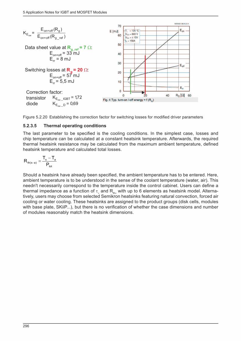
5 Application Notes for IGBT and MOSFET Modules
296
)R(E
)R(EK
ref_goffon+
goffon+Esw
72,1K IGBT_Esw
69,0K D_Esw
Correction factor:
transistor
diode
Data sheet value at Rg_ref = 7 W:
Eon+off = 33 mJ
Err = 8 mJ
Switching losses at Rg = 20 W:Eon+off = 57 mJ
Err = 5,5 mJ
=
=
=
Figure 5.2.20 Establishing the correction factor for switching losses for modifi ed driver parameters
5.2.3.5 Thermal operating conditions
The last parameter to be specifi ed is the cooling conditions. In the simplest case, losses and chip temperature can be calculated at a constant heatsink temperature. Afterwards, the required thermal heatsink resistance may be calculated from the maximum ambient temperature, defi ned heatsink temperature and calculated total losses.
tot
as)as(th
P
TTR
-=-
Should a heatsink have already been specifi ed, the ambient temperature has to be entered. Here, ambient temperature is to be understood in the sense of the coolant temperature (water, air). This needn't necessarily correspond to the temperature inside the control cabinet. Users can defi ne a thermal impedance as a function of τ
ν and R
thν with up to 6 elements as heatsink model. Alterna-
tively, users may choose from selected Semikron heatsinks featuring natural convection, forced air cooling or water cooling. These heatsinks are assigned to the product groups (disk cells, modules with base plate, SKiiP...), but there is no verifi cation of whether the case dimensions and number of modules reasonably match the heatsink dimensions.

5 Application Notes for IGBT and MOSFET Modules
297
Figure 5.2.21 Defi ning cooling conditions in SemiSel
Specifying cooling conditions requires engineering expertise which the software cannot provide. The infl uence of the component size, the number of components, and the distribution of heat sources to the thermal resistance of the heatsink R
th(s-a) have to be considered. Heatsink thermal
resistances are often given by the manufacturers to indicate evenly spread heat spread. In case of sporadic impression R
th is increased. Some parameters are given in chapter 55.3 as a guide-
line; for some SEMIKRON heatsinks, dependencies are specifi ed in terms of component size and quantity. To be able to infl uence R
th(s-a) , the user is offered a correction factor. This factor is multi-
plied by the database value for the selected heatsink to enable adjustment to the above-mentioned infl uences. The correction factor can also be used to adjust R
th of an actual heatsink to the value
for a heatsink provided in the program. Their size and weight should, however, be similar. The new value is displayed as R
th(s-a)* . R
th(s-a) is also dependent on the coolant volumetric fl ow rate. This may
be varied for the pre-defi ned heatsinks within certain limits.
When calculating T s it is important that the number of heat sources n is specifi ed. These are uni-
versally defi ned as switches. A three-phase IGBT inverter consists of 6 switches; 1 IGBT and the relevant inverse diode make up one switch. A switch may also consist of a parallel connection of several chosen components. This must also be defi ned. The upper image in Figure 5.2.22 shows a three-phase inverter comprising 3 half-bridge modules (GB). 6 switches are mounted on the heatsink; there is no parallel connection. In the other two examples, there is a parallel connection. The example in the middle shows one phase with 2 switches per heatsink, while in the example at the bottom, all of the 6 switches reside on one heatsink once again, but every switch consists of 2 modules connected in parallel. The total power dissipation on the heatsink adds up to
( ))D(tot)T(totpstot PPnnP +××=
n s = number of switches on the heatsink
n p = number of components connected in parallel in the switch
In a parallel connection, the inverter current is ideally divided between the number of parallel com-ponents.
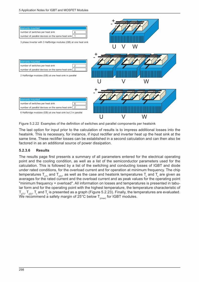
5 Application Notes for IGBT and MOSFET Modules
298
+-
U V W
+-
U V W
+-
U V W
elements mounted
6number of switches per heat sink
number of parallel devices on the same heat sink 1
elements mounted
2number of switches per heat sink
number of parallel devices on the same heat sink 2
elements mounted
6number of switches per heat sink
number of parallel devices on the same heat sink 2
3 phase Inverter with 3 Halfbridge modules (GB) at one heat sink
2 Halfbridge modules (GB) at one heat sink in parallel
6 Halfbridge modules (GB) at one heat sink but 2 in parallel
Figure 5.2.22 Examples of the defi nition of switches and parallel components per heatsink
The last option for input prior to the calculation of results is to impress additional losses into the heatsink. This is necessary, for instance, if input rectifi er and inverter heat up the heat sink at the same time. These rectifi er losses can be established in a second calculation and can then also be factored in as an additional source of power dissipation.
5.2.3.6 Results
The results page fi rst presents a summary of all parameters entered for the electrical operating point and the cooling condition, as well as a list of the semiconductor parameters used for the calculation. This is followed by a list of the switching and conducting losses of IGBT and diode under rated conditions, for the overload current and for operation at minimum frequency. The chip temperatures T
j(T) and T
j(D) , as well as the case and heatsink temperatures T
c and T
s are given as
averages for the rated current and the overload current and as peak values for the operating point "minimum frequency + overload". All information on losses and temperatures is presented in tabu-lar form and for the operating point with the highest temperature, the temperature characteristic of T
j(T) , T
j(D) , T
c and T
s is presented as a graph (Figure 5.2.23). Finally, the temperatures are evaluated.
We recommend a safety margin of 25°C below T j(max)
for IGBT modules.
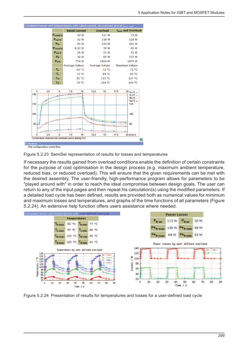
5 Application Notes for IGBT and MOSFET Modules
299
Figure 5.2.23 SemiSel representation of results for losses and temperatures
If necessary the results gained from overload conditions enable the defi nition of certain constraints for the purpose of cost optimisation in the design process (e.g. maximum ambient temperature, reduced bias, or reduced overload). This will ensure that the given requirements can be met with the desired assembly. The user-friendly, high-performance program allows for parameters to be "played around with" in order to reach the ideal compromise between design goals. The user can return to any of the input pages and then repeat his calculation(s) using the modifi ed parameters. If a detailed load cycle has been defi ned, results are provided both as numerical values for minimum and maximum losses and temperatures, and graphs of the time functions of all parameters (Figure 5.2.24). An extensive help function offers users assistance where needed.
Figure 5.2.24 Presentation of results for temperatures and losses for a user-defi ned load cycle
5 Application Notes for IGBT and MOSFET Modules
300
5.3 Cooling power modules
Here, the main focus will be on forced air cooling and water cooling, since these types of cooling cover 95% of all power module applications. Other cooling methods, such as evaporative cooling and spray cooling, and natural air cooling, too, will be mentioned. However, these are still of mi-nor importance for IGBT and MOSFET power modules. Details on natural air cooling and cooling plates are explained in chapter 4.2 in the context of (discrete) rectifi ers.
The extensive heat build-up in power modules caused by forward, switching and blocking losses has to be dissipated by means of heatsinks; these heatsinks provide an expanded surface for con-vection and radiation, spreading the heat fl ow as well as reducing the intensity of transient thermal processes. Due to their internal insulation, all of the power modules in a system can be mounted onto one common heatsink, which may also take on some function in the design construction, too (case, chassis etc.). Heat dissipation through a heatsink works on the principle that the heat is dissipated to the coolant either by direct heat conduction or via a heat carrier. Coolants may be air, water or aqueous mixtures, or (less frequently) insulation oil, which is circulated by the effect of gravity or using fans or pumps.
5.3.1 Thermal model of the cooling system
The thermal equation of the heatsink is as follows:
Q = α · A · ∆T = P tot
This result in the defi nition of the thermal resistance:
A
1
P
TR
tot
)as(
)as(th ×a=
D= -
-
(Q - dissipated heat quantity, α - heat-transfer coeffi cient, A - heat transfer area)
Since T s was measured at a certain point in order to determine ∆T
(s-a) , the value for R
th(s-a) only ap-
plies to this measuring point of ambient temperature (see chapter 5.3.2.4). Other measuring points will result in different values. To simplify analysis, a uniform heatsink temperature for all compo-nents is often assumed in other layouts containing several modules. Losses occurring in all of the heat sources on the heatsink are dissipated through the common R
th(s-a) .
The equation above for R th shows that a high number of fi ns makes sense in order to increase the
dissipation area. What must be ensured, however, is that the fl ow conditions are set in a way which will not excessively reduce the fl ow speed and hence the heat-transfer coeffi cient α. This explains, for example, why there are different optimisation criteria for heatsinks with natural and forced air cooling. In line with better heat penetration on the heatsinks as a result of higher power dissipa-tion, homogenous heat distribution or more even heat spread, the effective heat exchange area A
eff
increases and the effi ciency of the heatsink increases or R th(s-a)
decreases. Swirling the coolant as much as possible greatly increases the value of α, which also contributes to the reduction of R
th(s-a) .
In the explanation of power modules' thermal characteristics in chapter 5.2, the heatsink was ini-tially described in the thermal equivalent circuit diagram by one "RC element" only (R
th/(s-a) , Z
th(s-a) ).
However, with a sudden increase in power dissipation at t = 0 from P = 0 to P = Pm, the transient thermal impedance characteristic of the heatsink Z
th(s-a) versus time t is split up into several time
constants, as shown in Figure 5.3.6. From this, the total thermal impedance characteristic Z th(j-a)
of the assembly may be determined by adding the thermal impedance characteristics of the power module and the heat transfer to the heatsink. The Z
th curves can be described as the sum of n
exponential functions using the following equations:
å=n
t
-
n- ÷÷
ø
ö
çç
è
æ-××=D n
n
1
t
thm)as(the1RP)t(T

5 Application Notes for IGBT and MOSFET Modules
301
m
)as(
)as(thP
)t(T)t(Z
--
D=
It thus follows that
å=n
t
-
n- ÷÷
ø
ö
çç
è
æ-×= n
n
1
t
th)as(ththe1R)t(Z
The number ν of summands and the values for R thn
and τ ν are chosen such that a suffi cient approx-
imation of the curve shape can be produced with a reasonable amount of calculations involved, irrespective of the physical structure. The basis for determining values of R
th and τ
th is the existing
Z th curve. Mathematical programs and spreadsheets such as Excel (→ Solver) are able to solve
equation systems with a large number of unknown elements by setting the sum of error squares to zero (0) for a large number of interpolation nodes, as shown in the following equation.
0e1R)(tZ
2t
thna)-th(sth
n
=÷÷
ø
ö
çç
è
æ
÷÷
ø
ö
çç
è
æ-×- å nt
-
n
In order to rule out absurd solutions, a constraint must defi ne R th and τ
th > 0 sind. The number of
R th /τ
th pairs can be increased until the desired accuracy has been achieved. In most cases, 3...5
pairs are suffi cient.
5.3.2 Factors infl uencing thermal resistance
5.3.2.1 Number of heat sources
The number of heat sources spread across the heatsink has a crucial impact on R th(s-a)
. Unless ex-plicitly specifi ed otherwise, the values given by heatsink manufacturers apply to a large-area heat impression across the entire mounting surface. The closer we approach this ideal case with a large number of distributed heat sources, the better this theoretical R
th value can be reached. Measure-
ments are complex and time-consuming and manufacturer data on different confi gurations is hard to come by. FEM simulations could be a solution, since these simulations are especially meaning-ful whenever relative comparisons are to be made with known parameters. Figure 5.3.1 depicts simulations [56] of the same heatsink comprising 1 x (right) and 3 x 62 mm IGBT module(s) (left). For 3 modules the following applies:
K/W034,0
W1800
C40-C120R )as(th =
°°=-
The R th of the same heatsink for identical ambient conditions will increase to the following value if
just one module is mounted.
K/W0566,0
W600
C40-C74R )as(th =
°°=-
This is equivalent to a 65% increase. For some of their heatsinks, SEMIKRON specifi es R th in de-
pendence of the number of modules and module size (Figure 5.3.2). Unless thermal impedances have been given for different layouts, they can be adjusted by weighing R
thν with a correction factor
gained from the ratio of thermal resistances. The time constants of the thermal impedances will remain the same.
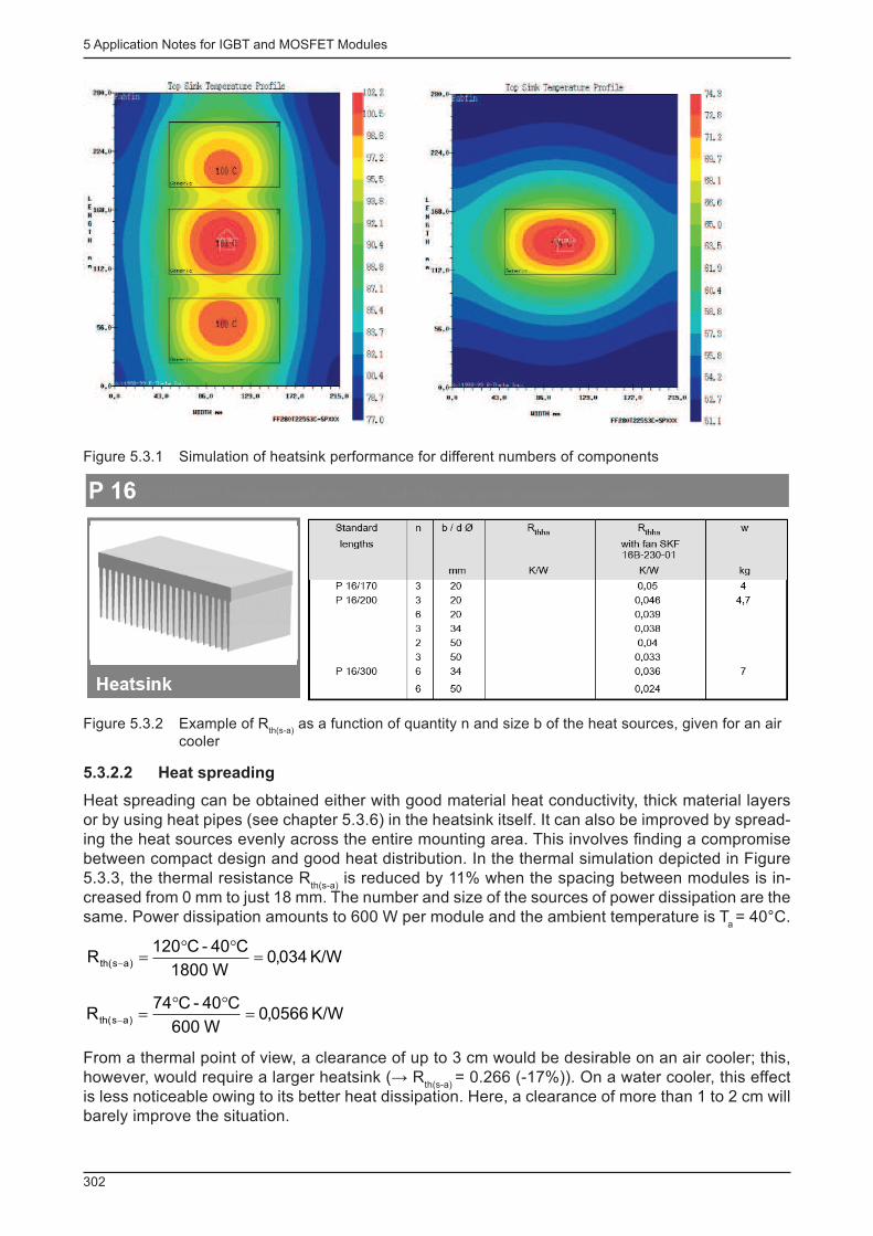
5 Application Notes for IGBT and MOSFET Modules
302
Figure 5.3.1 Simulation of heatsink performance for different numbers of components
Figure 5.3.2 Example of R th(s-a)
as a function of quantity n and size b of the heat sources, given for an air cooler
5.3.2.2 Heat spreading
Heat spreading can be obtained either with good material heat conductivity, thick material layers or by using heat pipes (see chapter 5.3.6) in the heatsink itself. It can also be improved by spread-ing the heat sources evenly across the entire mounting area. This involves fi nding a compromise between compact design and good heat distribution. In the thermal simulation depicted in Figure 5.3.3, the thermal resistance R
th(s-a) is reduced by 11% when the spacing between modules is in-
creased from 0 mm to just 18 mm. The number and size of the sources of power dissipation are the same. Power dissipation amounts to 600 W per module and the ambient temperature is T
a = 40°C.
K/W034,0
W1800
C40-C120R )as(th =
°°=-
K/W0566,0
W600
C40-C74R )as(th =
°°=-
From a thermal point of view, a clearance of up to 3 cm would be desirable on an air cooler; this, however, would require a larger heatsink (→ R
th(s-a) = 0.266 (-17%)). On a water cooler, this effect
is less noticeable owing to its better heat dissipation. Here, a clearance of more than 1 to 2 cm will barely improve the situation.
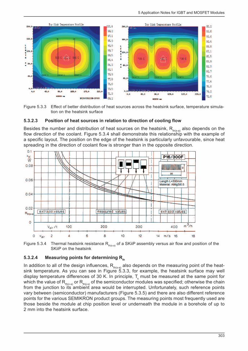
5 Application Notes for IGBT and MOSFET Modules
303
Figure 5.3.3 Effect of better distribution of heat sources across the heatsink surface, temperature simula-tion on the heatsink surface
5.3.2.3 Position of heat sources in relation to direction of cooling fl ow
Besides the number and distribution of heat sources on the heatsink, R th(s-a)
also depends on the fl ow direction of the coolant. Figure 5.3.4 shall demonstrate this relationship with the example of a specifi c layout. The position on the edge of the heatsink is particularly unfavourable, since heat spreading in the direction of coolant fl ow is stronger than in the opposite direction.
Figure 5.3.4 Thermal heatsink resistance R th(s-a)
of a SKiiP assembly versus air fl ow and position of the SKiiP on the heatsink
5.3.2.4 Measuring points for determining R th
In addition to all of the design infl uences, R th(s-a)
also depends on the measuring point of the heat-sink temperature. As you can see in Figure 5.3.3, for example, the heatsink surface may well display temperature differences of 30 K. In principle, T
s must be measured at the same point for
which the value of R th(c-s)
or R th(j-s)
of the semiconductor modules was specifi ed; otherwise the chain from the junction to its ambient area would be interrupted. Unfortunately, such reference points vary between (semiconductor) manufacturers (Figure 5.3.5) and there are also different reference points for the various SEMIKRON product groups. The measuring points most frequently used are those beside the module at chip position level or underneath the module in a borehole of up to 2 mm into the heatsink surface.
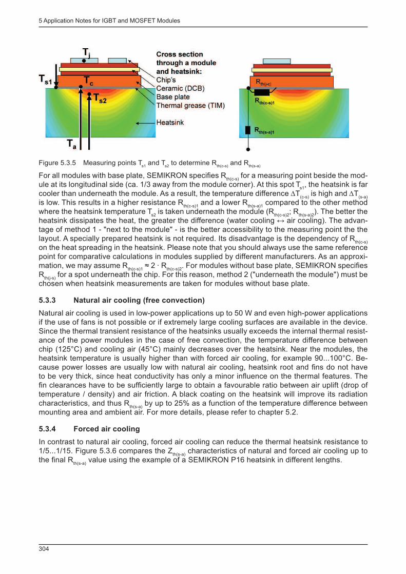
5 Application Notes for IGBT and MOSFET Modules
304
Figure 5.3.5 Measuring points T s1
and T s2
to determine R th(c-s)
and R th(s-a)
For all modules with base plate, SEMIKRON specifi es R th(c-s)
for a measuring point beside the mod-ule at its longitudinal side (ca. 1/3 away from the module corner). At this spot T
s1 , the heatsink is far
cooler than underneath the module. As a result, the temperature difference ∆T (c-s)
is high and ∆T (s-a)
is low. This results in a higher resistance R
th(c-s)1 and a lower R
th(s-a)1 compared to the other method
where the heatsink temperature T s2
is taken underneath the module (R th(c-s)2
; R th(s-a)2
). The better the heatsink dissipates the heat, the greater the difference (water cooling ↔ air cooling). The advan-tage of method 1 - "next to the module" - is the better accessibility to the measuring point the the layout. A specially prepared heatsink is not required. Its disadvantage is the dependency of R
th(c-s)
on the heat spreading in the heatsink. Please note that you should always use the same reference point for comparative calculations in modules supplied by different manufacturers. As an approxi-mation, we may assume R
th(c-s)1 ≈ 2 · R
th(c-s)2 . For modules without base plate, SEMIKRON specifi es
R th(j-s)
for a spot underneath the chip. For this reason, method 2 ("underneath the module") must be chosen when heatsink measurements are taken for modules without base plate.
5.3.3 Natural air cooling (free convection)
Natural air cooling is used in low-power applications up to 50 W and even high-power applications if the use of fans is not possible or if extremely large cooling surfaces are available in the device. Since the thermal transient resistance of the heatsinks usually exceeds the internal thermal resist-ance of the power modules in the case of free convection, the temperature difference between chip (125°C) and cooling air (45°C) mainly decreases over the heatsink. Near the modules, the heatsink temperature is usually higher than with forced air cooling, for example 90...100°C. Be-cause power losses are usually low with natural air cooling, heatsink root and fi ns do not have to be very thick, since heat conductivity has only a minor infl uence on the thermal features. The fi n clearances have to be suffi ciently large to obtain a favourable ratio between air uplift (drop of temperature / density) and air friction. A black coating on the heatsink will improve its radiation characteristics, and thus R
th(s-a) by up to 25% as a function of the temperature difference between
mounting area and ambient air. For more details, please refer to chapter 5.2.
5.3.4 Forced air cooling
In contrast to natural air cooling, forced air cooling can reduce the thermal heatsink resistance to 1/5...1/15. Figure 5.3.6 compares the Z
th(s-a) characteristics of natural and forced air cooling up to
the fi nal R th(s-a)
value using the example of a SEMIKRON P16 heatsink in different lengths.
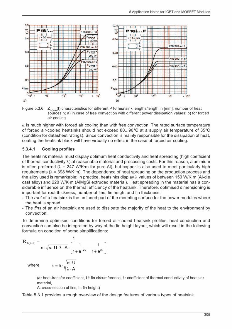
5 Application Notes for IGBT and MOSFET Modules
305
Figure 5.3.6 Z th(s-a)
(t) characteristics for different P16 heatsink lengths/length in [mm], number of heat sources n; a) in case of free convection with different power dissipation values; b) for forced air cooling
α is much higher with forced air cooling than with free convection. The rated surface temperature of forced air-cooled heatsinks should not exceed 80...90°C at a supply air temperature of 35°C (condition for datasheet ratings). Since convection is mainly responsible for the dissipation of heat, coating the heatsink black will have virtually no effect in the case of forced air cooling.
5.3.4.1 Cooling profi les
The heatsink material must display optimum heat conductivity and heat spreading (high coeffi cient of thermal conductivity λ) at reasonable material and processing costs. For this reason, aluminium is often preferred (λ = 247 W/K·m for pure Al), but copper is also used to meet particularly high requirements (λ = 398 W/K·m). The dependence of heat spreading on the production process and the alloy used is remarkable; in practice, heatsinks display λ values of between 150 W/K·m (Al-die cast alloy) and 220 W/K·m (AlMgSi extruded material). Heat spreading in the material has a con-siderable infl uence on the thermal effi ciency of the heatsink. Therefore, optimised dimensioning is important for root thickness, number of fi ns, fi n height and fi n thickness: - The root of a heatsink is the unfi nned part of the mounting surface for the power modules where the heat is spread.
- The fi ns of an air heatsink are used to dissipate the majority of the heat to the environment by convection.
To determine optimised conditions for forced air-cooled heatsink profi les, heat conduction and convection can also be integrated by way of the fi n height layout, which will result in the following formula on condition of some simplifi cations:
úûù
êëé
+-
+××l××a×
=
kk-
-
22
)as(th
e1
1
e1
1AUn
1R
where A
Uh
×l×a
×=k
(α: heat-transfer coeffi cient, U: fi n circumference, λ: coeffi cient of thermal conductivity of heatsink material, A: cross-section of fi ns, h: fi n height)
Table 5.3.1 provides a rough overview of the design features of various types of heatsink.

5 Application Notes for IGBT and MOSFET Modules
306
Thin root Thick root
Many fi ns Few fi ns
Lower R th(s-a)
Higher R th(s-a)
But:
Low overload capacity (e.g. for pumps) High overload capacity (e.g. for lifts)
Short time constants Long time constants
Little heat spread Good heat spread
High pressure drop – less air Low pressure drop – more air
Sensitive to dirt Less sensitive to dirt
Table 5.3.1 Properties and selection criteria for different heatsink profi les
5.3.4.2 Pressure drop and air volume
R th(s-a)
continues to be mainly determined by the rate of air fl ow per time V air
/t depending on the average cooling air velocity v
air and the transfer cross section A:
V air
/t = v air
· A
Instead of the assumed laminar air fl ow, air swirling on the fi n surfaces will induce turbulent fl ow conditions which will improve heat dissipation to air, provided the fi n surfaces are set out accord-ingly. Of course, it is not just the static, but also the transient thermal resistance (thermal imped-ance) Z
th which is reduced by forced air cooling. Figure 5.3.6 shows Z
th(s-a) characteristics up to the
fi nal R th(s-a)
value for natural and forced air cooling in a SEMIKRON P16 heatsink. Time behaviour also changes by a power of ten. While for natural air cooling the static end value will only have been reached after 2,000…3,000 s, in the case of forced air cooling this process is completed after just 200...300 s.
Increasing the number of fi ns and fi n width will reduce the transfer cross section of the heatsink. As with increased heatsink length, the pressure drop in the cooling air ∆p rises and the volumetric fl ow rate decreases. This is a counter-effect to extending the cooling surface. For this reason, each fan has an optimum with regard to fl ow cross section, heatsink length and volumetric fl ow rate. Heat dissipation is dependent on the fan properties, which are described in the fan characteristic ∆p = f(V
air /t) (Figure 5.3.7).
The intersection of the characteristic fan curve and the pressure drop curves for the heatsinks ∆p = f(V
air /t, L) enables the volumetric fl ow rate at the operating point to be determined according to
Figure 5.3.7. When integrating the fan characteristic, the permissible operating voltage fl uctuation (e.g. 230 V +/- 10%) must also be taken into account. Suffi cient cooling has to be ensured even when a minimum voltage is applied, i.e. when there is less air fl ow. The heat transfer resistance R
th(s-a) of the heatsink layout (Figure 5.3.8) is a function of the determined volumetric fl ow rate.
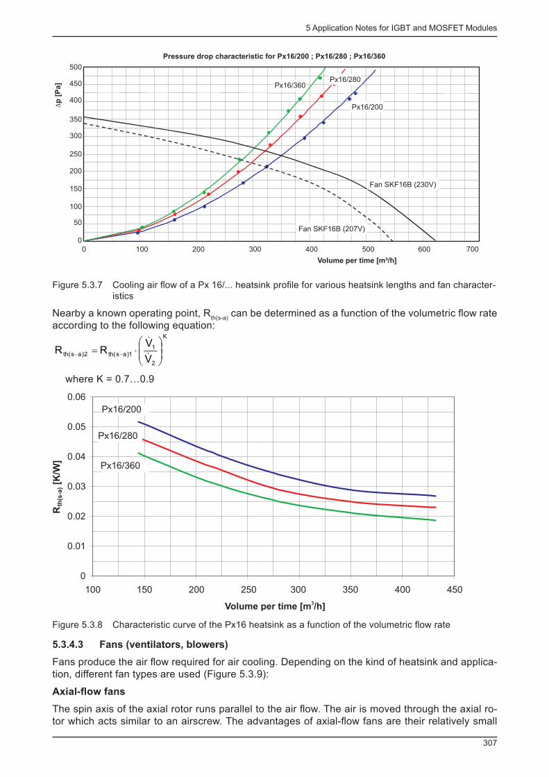
5 Application Notes for IGBT and MOSFET Modules
307
Pressure drop characteristic for Px16/200 ; Px16/280 ; Px16/360
500
0 100 200 300 400 500 600 700
Volume per time [m³/h]
450
400
350
300
250
200
150
100
50
0
Px16/200
Px16/360
Dp
[Pa]
Fan SKF16B (230V)
Fan SKF16B (207V)
Px16/280
Figure 5.3.7 Cooling air fl ow of a Px 16/... heatsink profi le for various heatsink lengths and fan character-istics
Nearby a known operating point, R th(s-a)
can be determined as a function of the volumetric fl ow rate according to the following equation:
K
2
11)as(th2)as(th
V
VRR ÷÷
ø
öççè
æ×= -- &
&
where K = 0.7…0.9
0
0.01
0.02
0.03
0.04
0.05
0.06
100 150 200 250 300 350 400 450
th(s
-a)[K
/W]
Px16/200
Px16/360
Px16/280
R
Volume per time [m /h]3
Figure 5.3.8 Characteristic curve of the Px16 heatsink as a function of the volumetric fl ow rate
5.3.4.3 Fans (ventilators, blowers)
Fans produce the air fl ow required for air cooling. Depending on the kind of heatsink and applica-tion, different fan types are used (Figure 5.3.9):
Axial-fl ow fans
The spin axis of the axial rotor runs parallel to the air fl ow. The air is moved through the axial ro-tor which acts similar to an airscrew. The advantages of axial-fl ow fans are their relatively small

5 Application Notes for IGBT and MOSFET Modules
308
dimensions in relation to the high air fl ow rate handled. Their disadvantage is the increase in pres-sure compared to radial-fl ow fans.
Radial-fl ow fans or centrifugal fans
Radial-fl ow fans (Figure 5.3.10) are used whenever, unlike axial-fl ow fans, a higher pressure in-crease for the same amount of air is important. The air is sucked in parallel or axial to the drive axis of the radial-fl ow fan, and defl ected by 90° as a result of the rotation of the radial rotor and blown out in a radial direction. In order to minimise pressure losses due to the high exit velocity of air out of the radial-fl ow fan, care must be taken to continue the air chanelling, e.g. by using a diffuser.
Tangential or cross-fl ow fan
Cross-fl ow fans have an intake and blow-out slot across their entire length. Air is sucked into the interior of the rotor through the intake slot, where it is swirled, defl ected and blown out highly ho-mogenously. Cross-fl ow fans provide a high air fl ow rate even at low speeds and can therefore be constructed to emit relatively low noise. The rotor length and the outlet slot are matched to the heatsink width.
Figure 5.3.9 a) Axial-fl ow fan, b) Radial-fl ow fan, c) Cross-fl ow fan
Figure 5.3.10 Set of 3 diode-half-bridge modules in a three-phase rectifi er circuit on a cooling profi le with radial-fl ow fan
5.3.4.4 Operating height
The amount of heat to be dissipated depends on the atmospheric pressure and the density of the cooling air. Air density, and hence cooling effi ciency, decreases as the operating height increases. Decreasing air density deteriorates heat dissipation. Heatsink effi ciency also deteriorates. To fac-

5 Application Notes for IGBT and MOSFET Modules
309
tor this in, it is necessary to reduce the inverter power, or to multiply R th for thermal rating by a cor-
rection factor in accordance with Table 5.3.2 [57].
Height [m / ft] Performance reduction Correction factor for R th(s-a)
0 / sea level 1 1
1000 / 3000 0.95 1.05
1500 / 5000 0.90 1.11
2000 / 7000 0.86 1.16
3000 / 10000 0.8 1.25
3500 / 12000 0.75 1.33
Table 5.3.2 Impact of operating height above sea level on thermal resistance
These performance constraints also apply to water coolers if the cooling water temperature is regulated by means of an air-cooled heat exchanger.
5.3.5 Water cooling
Water cooling in power modules can be used for very high power inverters (MW range) as well as for low-power devices which already have a water cycle for operating reasons (e.g. car drives, galvanic installations, inductive heating). In most cases, the admission temperature of the coolant values is as much as 50...70°C when the heat of the coolant is directly dissipated to the atmos-phere; in industrial plants with active heat exchangers, the temperature is about 15...25°C. The temperature difference between heatsink surface and coolant, which is lower than for air cooling, may be utilised in two ways: - increased power density, but with high dynamic ∆T
j of chip temperature per load cycle (for limits
for module life see chapter 2.7), or - low chip temperature, long module life.
Figure 5.3.11 shows an example of water cooling of a 6-fold SKiiP on a water-cooled heatsink.
Figure 5.3.11 SKiiP4 layout with water-cooled heatsink
The following factors infl uence the thermal resistance in a liquid cooler: - the contact area to the coolant (e.g. number of cooling channels) - the volumetric fl ow rate as a function of the pressure drop (chapter 5.3.5.1) - the heat storage capability of the coolant (chapter 5.3.5.2) - turbulence in the water fl ow - heat conduction and spreading in the heatsink (heatsink material) - the coolant temperature (depending on viscosity and density)
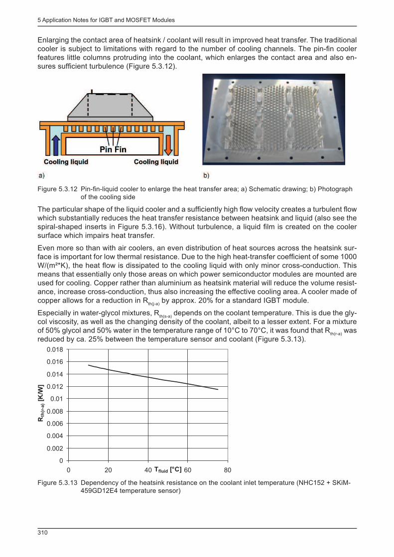
5 Application Notes for IGBT and MOSFET Modules
310
Enlarging the contact area of heatsink / coolant will result in improved heat transfer. The traditional cooler is subject to limitations with regard to the number of cooling channels. The pin-fi n cooler features little columns protruding into the coolant, which enlarges the contact area and also en-sures suffi cient turbulence (Figure 5.3.12).
Figure 5.3.12 Pin-fi n-liquid cooler to enlarge the heat transfer area; a) Schematic drawing; b) Photograph of the cooling side
The particular shape of the liquid cooler and a suffi ciently high fl ow velocity creates a turbulent fl ow which substantially reduces the heat transfer resistance between heatsink and liquid (also see the spiral-shaped inserts in Figure 5.3.16). Without turbulence, a liquid fi lm is created on the cooler surface which impairs heat transfer.
Even more so than with air coolers, an even distribution of heat sources across the heatsink sur-face is important for low thermal resistance. Due to the high heat-transfer coeffi cient of some 1000 W/(m²*K), the heat fl ow is dissipated to the cooling liquid with only minor cross-conduction. This means that essentially only those areas on which power semiconductor modules are mounted are used for cooling. Copper rather than aluminium as heatsink material will reduce the volume resist-ance, increase cross-conduction, thus also increasing the effective cooling area. A cooler made of copper allows for a reduction in R
th(j-a) by approx. 20% for a standard IGBT module.
Especially in water-glycol mixtures, R th(s-a)
depends on the coolant temperature. This is due the gly-col viscosity, as well as the changing density of the coolant, albeit to a lesser extent. For a mixture of 50% glycol and 50% water in the temperature range of 10°C to 70°C, it was found that R
th(r-a) was
reduced by ca. 25% between the temperature sensor and coolant (Figure 5.3.13).
0
0.002
0.004
0.006
0.008
0.01
0.012
0.014
0.016
0.018
0 20 40 60 80Tfluid [°C]
Rth
(r-a
)[K
/W]
Figure 5.3.13 Dependency of the heatsink resistance on the coolant inlet temperature (NHC152 + SKiM-459GD12E4 temperature sensor)
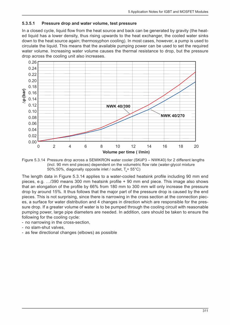
5 Application Notes for IGBT and MOSFET Modules
311
5.3.5.1 Pressure drop and water volume, test pressure
In a closed cycle, liquid fl ow from the heat source and back can be generated by gravity (the heat-ed liquid has a lower density, thus rising upwards to the heat exchanger, the cooled water sinks down to the heat source again; thermosyphon cooling). In most cases, however, a pump is used to circulate the liquid. This means that the available pumping power can be used to set the required water volume. Increasing water volume causes the thermal resistance to drop, but the pressure drop across the cooling unit also increases.
0.00
0.02
0.04
0.06
0.08
0.10
0.12
0.14
0.16
0.18
0.20
0.22
0.24
0.26
0 2 4 6 8 10 12 14 16 18 20
Volume per time ( l/min)
Dp
(ba
r)
NWK 40/390
NWK 40/270
Figure 5.3.14 Pressure drop across a SEMIKRON water cooler (SKiiP3 – NWK40) for 2 different lengths (incl. 90 mm end pieces) dependent on the volumetric fl ow rate (water-glycol mixture 50%:50%, diagonally opposite inlet / outlet, T
a = 55°C)
The length data in Figure 5.3.14 applies to a water-cooled heatsink profi le including 90 mm end pieces, e.g. …/390 means 300 mm heatsink profi le + 90 mm end piece. This image also shows that an elongation of the profi le by 66% from 180 mm to 300 mm will only increase the pressure drop by around 15%. It thus follows that the major part of the pressure drop is caused by the end pieces. This is not surprising, since there is narrowing in the cross section at the connection piec-es, a surface for water distribution and 4 changes in direction which are responsible for the pres-sure drop. If a greater volume of water is to be pumped through the cooling circuit with reasonable pumping power, large pipe diameters are needed. In addition, care should be taken to ensure the following for the cooling cycle: - no narrowing in the cross-section, - no slam-shut valves, - as few directional changes (elbows) as possible
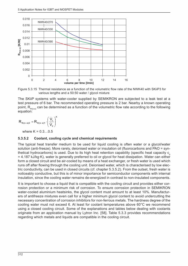
5 Application Notes for IGBT and MOSFET Modules
312
0
0.002
0.004
0.006
0.008
0.01
0.012
0.014
0.016
0.018
0 2 4 6 8 10 12 14 16volume per time [l/min]
Rth
(s-a
)[K
/W]
NWK40/270
NWK40/390
NWK40/330
Figure 5.3.15 Thermal resistance as a function of the volumetric fl ow rate of the NWK40 with SKiiP3 for various lengths and a 50:50 water / glycol mixture
The SKiiP systems with water-cooler supplied by SEMIKRON are subjected to a leak test at a test pressure of 6 bar. The recommended operating pressure is 2 bar. Nearby a known operating point, R
th(s-a) can be determined as a function of the volumetric fl ow rate according to the following
equation:
K
2
11)as(th2)as(th
V
VRR ÷÷
ø
öççè
æ×= -- &
&
where K = 0.3…0.5
5.3.5.2 Coolant, cooling cycle and chemical requirements
The typical heat transfer medium to be used for liquid cooling is often water or a glycol/water solution (anti-freeze). More rarely, deionised water or insulation oil (fl uorocarbons and PAO = syn-thetical hydrocarbons) is used. Due to its high heat retention capability (specifi c heat capacity c
p
= 4.187 kJ/kg·K), water is generally preferred to oil or glycol for heat dissipation. Water can either form a closed circuit and be air-cooled by means of a heat exchanger, or fresh water is used which runs off after fl owing through the cooling unit. Deionised water, which is characterised by low elec-tric conductivity, can be used in closed circuits (cf. chapter 5.3.5.2). From the outset, fresh water is noticeably conductive, but this is of minor importance for semiconductor components with internal insulation, since the cooling water remains de-energized in contrast to non-insulated components.
It is important to choose a liquid that is compatible with the cooling circuit and provides either cor-rosion protection or a minimum risk of corrosion. To ensure corrosion protection in SEMIKRON water-cooled aluminium heatsinks, the glycol content must amount to at least 10%. Manufactur-ers of antifreeze mixtures even call for a higher minimum glycol content to avoid undercutting the necessary concentration of corrosion inhibitors for non-ferrous metals. The hardness degree of the cooling water must not exceed 6. At least for coolant temperatures above 60°C we recommend using a closed cooling circuit. Some of the explanations and tables below dealing with coolants originate from an application manual by Lytron Inc. [58]. Table 5.3.3 provides recommendations regarding which metals and liquids are compatible in the cooling circuit.
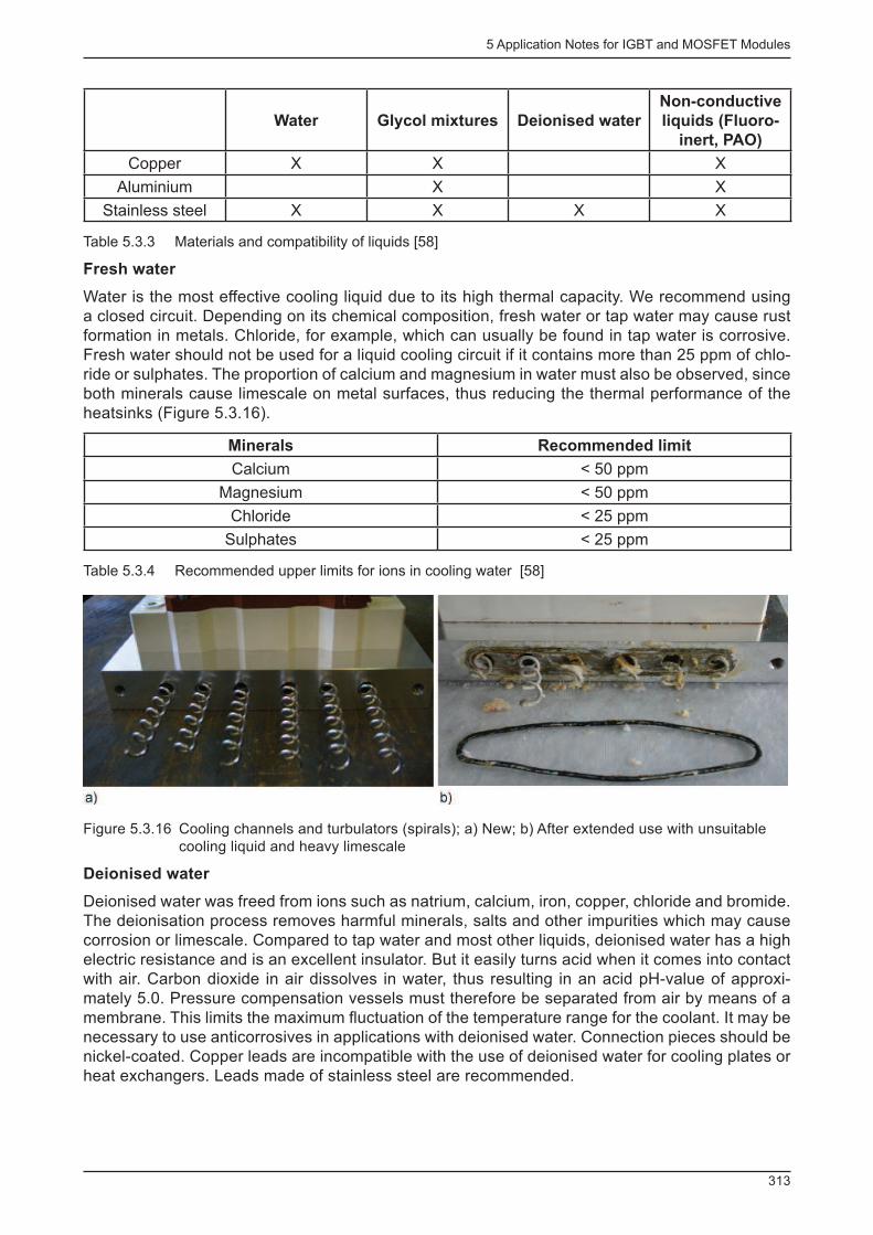
5 Application Notes for IGBT and MOSFET Modules
313
Water Glycol mixtures Deionised water
Non-conductive
liquids (Fluoro-
inert, PAO)
Copper X X X
Aluminium X X
Stainless steel X X X X
Table 5.3.3 Materials and compatibility of liquids [58]
Fresh water
Water is the most effective cooling liquid due to its high thermal capacity. We recommend using a closed circuit. Depending on its chemical composition, fresh water or tap water may cause rust formation in metals. Chloride, for example, which can usually be found in tap water is corrosive. Fresh water should not be used for a liquid cooling circuit if it contains more than 25 ppm of chlo-ride or sulphates. The proportion of calcium and magnesium in water must also be observed, since both minerals cause limescale on metal surfaces, thus reducing the thermal performance of the heatsinks (Figure 5.3.16).
Minerals Recommended limit
Calcium < 50 ppm
Magnesium < 50 ppm
Chloride < 25 ppm
Sulphates < 25 ppm
Table 5.3.4 Recommended upper limits for ions in cooling water [58]
Figure 5.3.16 Cooling channels and turbulators (spirals); a) New; b) After extended use with unsuitable cooling liquid and heavy limescale
Deionised water
Deionised water was freed from ions such as natrium, calcium, iron, copper, chloride and bromide. The deionisation process removes harmful minerals, salts and other impurities which may cause corrosion or limescale. Compared to tap water and most other liquids, deionised water has a high electric resistance and is an excellent insulator. But it easily turns acid when it comes into contact with air. Carbon dioxide in air dissolves in water, thus resulting in an acid pH-value of approxi-mately 5.0. Pressure compensation vessels must therefore be separated from air by means of a membrane. This limits the maximum fl uctuation of the temperature range for the coolant. It may be necessary to use anticorrosives in applications with deionised water. Connection pieces should be nickel-coated. Copper leads are incompatible with the use of deionised water for cooling plates or heat exchangers. Leads made of stainless steel are recommended.

5 Application Notes for IGBT and MOSFET Modules
314
Inhibited glycol and aqueous solutions
Due to the corrosive effect of water and the often necessary frost-resistance, open or closed cir-cuits with pure water are hardly ever used. E thylene G lycol W ater (EWG) and P ropylene G lycol W ater (PWG) are the two most frequently used solutions in liquid cooling applications. Ethylene glycol has positive thermal properties such as a high boiling point, low freezing point, stability across a wide temperature range, a relatively high specifi c heat capacity and thermal conductiv-ity. It also features low viscosity, meaning the piping requirements are less strict. PGW is used for applications where toxicity might be a problem. The glycol used in cars should not, however, be used in a cooling system or heat exchanger, since it contains a silicate-based rust inhibitor. These preventives may turn solid and cause deposits to form on the surfaces of heat exchangers, in do-ing so impairing their effi ciency. Glycol solutions should contain an anticorrosion agent.
By adding glycol, for example, the heat retention capability of the coolant will diminish (e.g. 3.4 J/(kg*(kg·K) for an addition of 50% glycol and a coolant temperature of 40°C). Since the viscosity and specifi c weight of the coolant will increase, the thermal resistance from heatsink to coolant R
th(s-a) will increase substantially together in line with the percentage of glycol. Compared to pure
water, 10% glycol will cause an increase in R th of around 15%, while adding 50% glycol will cause
an increase of 50...60%. If the glycol content is increased to as much as 90%, R th will double.
Please note that these statements also depend on the fl ow conditions in the heatsink and the cool-ant temperature.
Improvement Rth(s-a) with 10% Glycol instead of 50%
0%
5%
10%
15%
20%
25%
30%
35%
0 5 10 15 20 25l/min
Rth
(s-a
)[K
/W]
Figure 5.3.17 Infl uence of water-glycol mixture ratio on R th(s-a)
for different fl ow rates
5.3.5.3 Mounting direction and venting
When setting up the cooling circuit, care must be taken that cooling is not blocked by air bubble build-up. The best mounting set-up therefore consists of vertical channels, while the worst is hori-zontal channels on top of each another, since the top channel accumulates the air bubbles (Figure 5.3.18).
The preferred fl ow direction is upwards with the inlet at the bottom and the outlet at the top in the control cabinet. Loops in the water fl ow, i.e. an "up and down" arrangement in the cabinet is dis-advantageous. In that case, vent valves would be required in the cooling circuit above the power semiconductors. After the cooling unit has been fi lled, a test run with the highest fl ow rate should be performed for an extended period of time (> 0.5 h) without exposing the unit to normal electrical operation. A high fl ow rate (l/min) may remove existing air bubbles that might have been generated when the unit was fi rst set up.
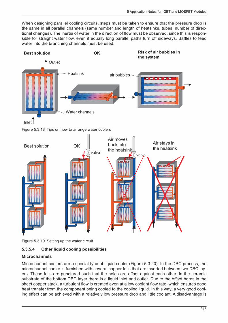
5 Application Notes for IGBT and MOSFET Modules
315
When designing parallel cooling circuits, steps must be taken to ensure that the pressure drop is the same in all parallel channels (same number and length of heatsinks, tubes, number of direc-tional changes). The inertia of water in the direction of fl ow must be observed, since this is respon-sible for straight water fl ow, even if equally long parallel paths turn off sideways. Baffl es to feed water into the branching channels must be used.
Best solution OK Risk of air bubbles in
the system
Heatsink
Water channels
Inlet
Outlet
air bubbles
Figure 5.3.18 Tips on how to arrange water coolers
Best solution OK
Air moves
back into
the heatsink
Air stays in
the heatsinkvalve
valve
Figure 5.3.19 Setting up the water circuit
5.3.5.4 Other liquid cooling possibilities
Microchannels
Microchannel coolers are a special type of liquid cooler (Figure 5.3.20). In the DBC process, the microchannel cooler is furnished with several copper foils that are inserted between two DBC lay-ers. These foils are punctured such that the holes are offset against each other. In the ceramic substrate of the bottom DBC layer there is a liquid inlet and outlet. Due to the offset bores in the sheet copper stack, a turbulent fl ow is created even at a low coolant fl ow rate, which ensures good heat transfer from the component being cooled to the cooling liquid. In this way, a very good cool-ing effect can be achieved with a relatively low pressure drop and little coolant. A disadvantage is
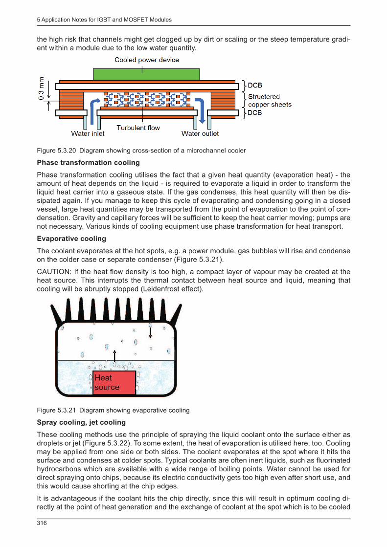
5 Application Notes for IGBT and MOSFET Modules
316
the high risk that channels might get clogged up by dirt or scaling or the steep temperature gradi-ent within a module due to the low water quantity.
Figure 5.3.20 Diagram showing cross-section of a microchannel cooler
Phase transformation cooling
Phase transformation cooling utilises the fact that a given heat quantity (evaporation heat) - the amount of heat depends on the liquid - is required to evaporate a liquid in order to transform the liquid heat carrier into a gaseous state. If the gas condenses, this heat quantity will then be dis-sipated again. If you manage to keep this cycle of evaporating and condensing going in a closed vessel, large heat quantities may be transported from the point of evaporation to the point of con-densation. Gravity and capillary forces will be suffi cient to keep the heat carrier moving; pumps are not necessary. Various kinds of cooling equipment use phase transformation for heat transport.
Evaporative cooling
The coolant evaporates at the hot spots, e.g. a power module, gas bubbles will rise and condense on the colder case or separate condenser (Figure 5.3.21).
CAUTION: If the heat fl ow density is too high, a compact layer of vapour may be created at the heat source. This interrupts the thermal contact between heat source and liquid, meaning that cooling will be abruptly stopped (Leidenfrost effect).
Figure 5.3.21 Diagram showing evaporative cooling
Spray cooling, jet cooling
These cooling methods use the principle of spraying the liquid coolant onto the surface either as droplets or jet (Figure 5.3.22). To some extent, the heat of evaporation is utilised here, too. Cooling may be applied from one side or both sides. The coolant evaporates at the spot where it hits the surface and condenses at colder spots. Typical coolants are often inert liquids, such as fl uorinated hydrocarbons which are available with a wide range of boiling points. Water cannot be used for direct spraying onto chips, because its electric conductivity gets too high even after short use, and this would cause shorting at the chip edges.
It is advantageous if the coolant hits the chip directly, since this will result in optimum cooling di-rectly at the point of heat generation and the exchange of coolant at the spot which is to be cooled
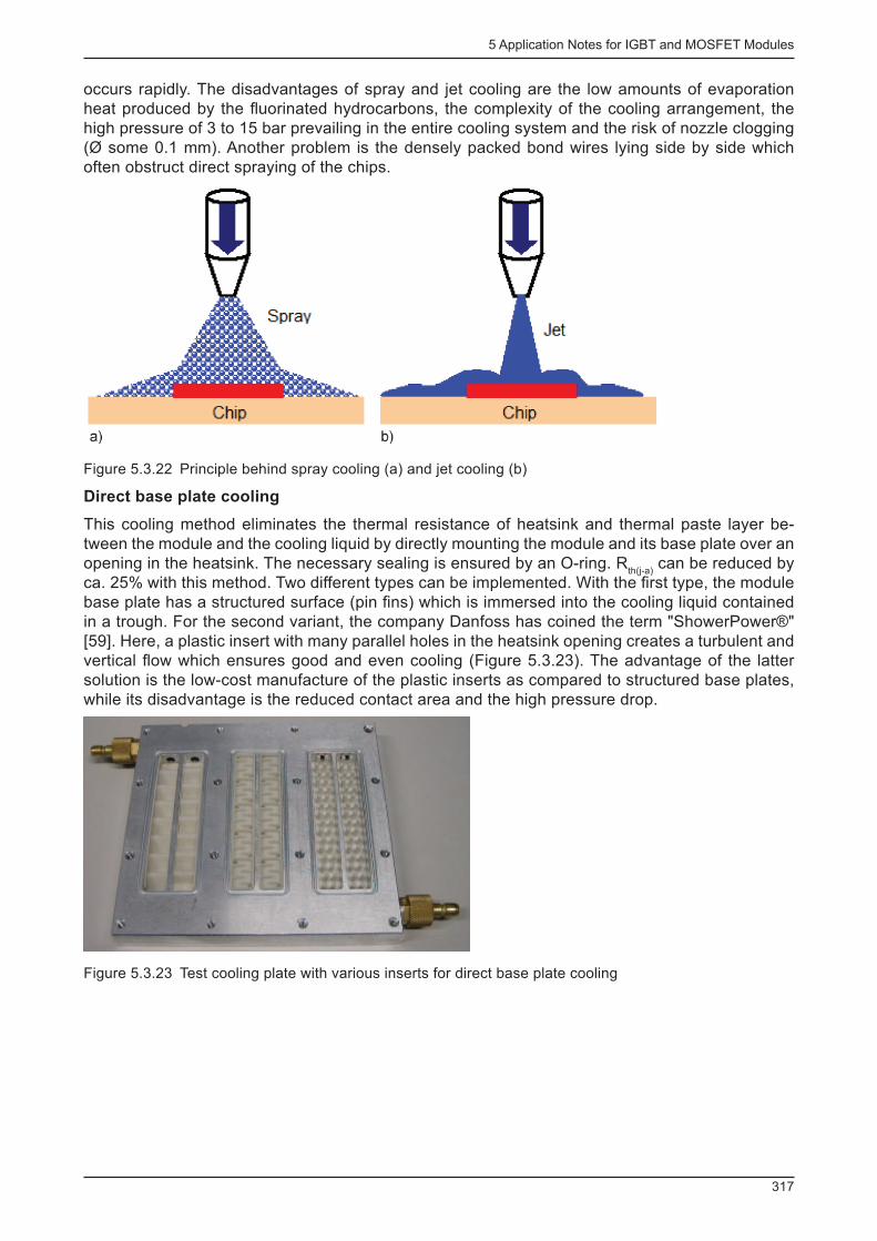
5 Application Notes for IGBT and MOSFET Modules
317
occurs rapidly. The disadvantages of spray and jet cooling are the low amounts of evaporation heat produced by the fl uorinated hydrocarbons, the complexity of the cooling arrangement, the high pressure of 3 to 15 bar prevailing in the entire cooling system and the risk of nozzle clogging (Ø some 0.1 mm). Another problem is the densely packed bond wires lying side by side which often obstruct direct spraying of the chips.
Figure 5.3.22 Principle behind spray cooling (a) and jet cooling (b)
Direct base plate cooling
This cooling method eliminates the thermal resistance of heatsink and thermal paste layer be-tween the module and the cooling liquid by directly mounting the module and its base plate over an opening in the heatsink. The necessary sealing is ensured by an O-ring. R
th(j-a) can be reduced by
ca. 25% with this method. Two different types can be implemented. With the fi rst type, the module base plate has a structured surface (pin fi ns) which is immersed into the cooling liquid contained in a trough. For the second variant, the company Danfoss has coined the term "ShowerPower®" [59]. Here, a plastic insert with many parallel holes in the heatsink opening creates a turbulent and vertical fl ow which ensures good and even cooling (Figure 5.3.23). The advantage of the latter solution is the low-cost manufacture of the plastic inserts as compared to structured base plates, while its disadvantage is the reduced contact area and the high pressure drop.
Figure 5.3.23 Test cooling plate with various inserts for direct base plate cooling
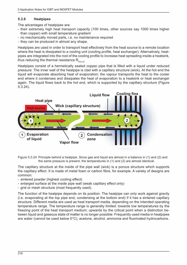
5 Application Notes for IGBT and MOSFET Modules
318
5.3.6 Heatpipes
The advantages of heatpipes are: - their extremely high heat transport capacity (100 times, other sources say 1000 times higher than copper) with small temperature gradient
- no mechanically moved parts, i.e. no maintenance required - they can be produced in almost any shape.
Heatpipes are used in order to transport heat effectively from the heat source to a remote location where the heat is dissipated to a cooling unit (cooling profi le, heat exchanger). Alternatively, heat-pipes are integrated into the root of the cooling profi le to increase heat spreading inside a heatsink, thus reducing the thermal resistance R
th(s-a) .
Heatpipes consist of a hermetically sealed copper pipe that is fi lled with a liquid under reduced pressure. The inner wall of the heatpipe is clad with a capillary structure (wick). At the hot end the liquid will evaporate absorbing heat of evaporation; the vapour transports the heat to the cooler end where it condenses and dissipates the heat of evaporation to a heatsink or heat exchanger again. The liquid fl ows back to the hot end, which is supported by the capillary structure (Figure 5.3.24).
Heat source
Heat pipe
Wick (capillary structure)
21
1 Evaporation
of liquid2 Condensation
zoneVapor flow
Liquid flow Cooling fins
Figure 5.3.24 Principle behind a heatpipe. Since gas and liquid are almost in a balance in (1) and (2) and the same pressure is present, the temperatures in (1) and (2) are almost identical.
The capillary structure at the inside of the pipe wall (wick) is a porous structure which supports the capillary effect. It is made of metal foam or carbon fi bre, for example. A variety of designs are common: - sintered powder (highest cooling effect) - enlarged surface at the inside pipe wall (weak capillary effect only) - grid or mesh structure (most frequently used).
The function of the heatpipe depends on its position. The heatpipe can only work against gravity (i.e. evaporating at the top pipe end, condensing at the bottom end) if it has a sintered capillary structure. Different media are used as heat transport media, depending on the intended operating temperature range. The temperature range is generally limited: towards low temperatures by the freezing point of the heat transport medium; upwards by the critical point when a distinction be-tween liquid and gaseous state of matter is no longer possible. Frequently used media in heatpipes are water (cannot be used below 0°C), acetone, alcohol, ammonia and fl uorinated hydrocarbons.
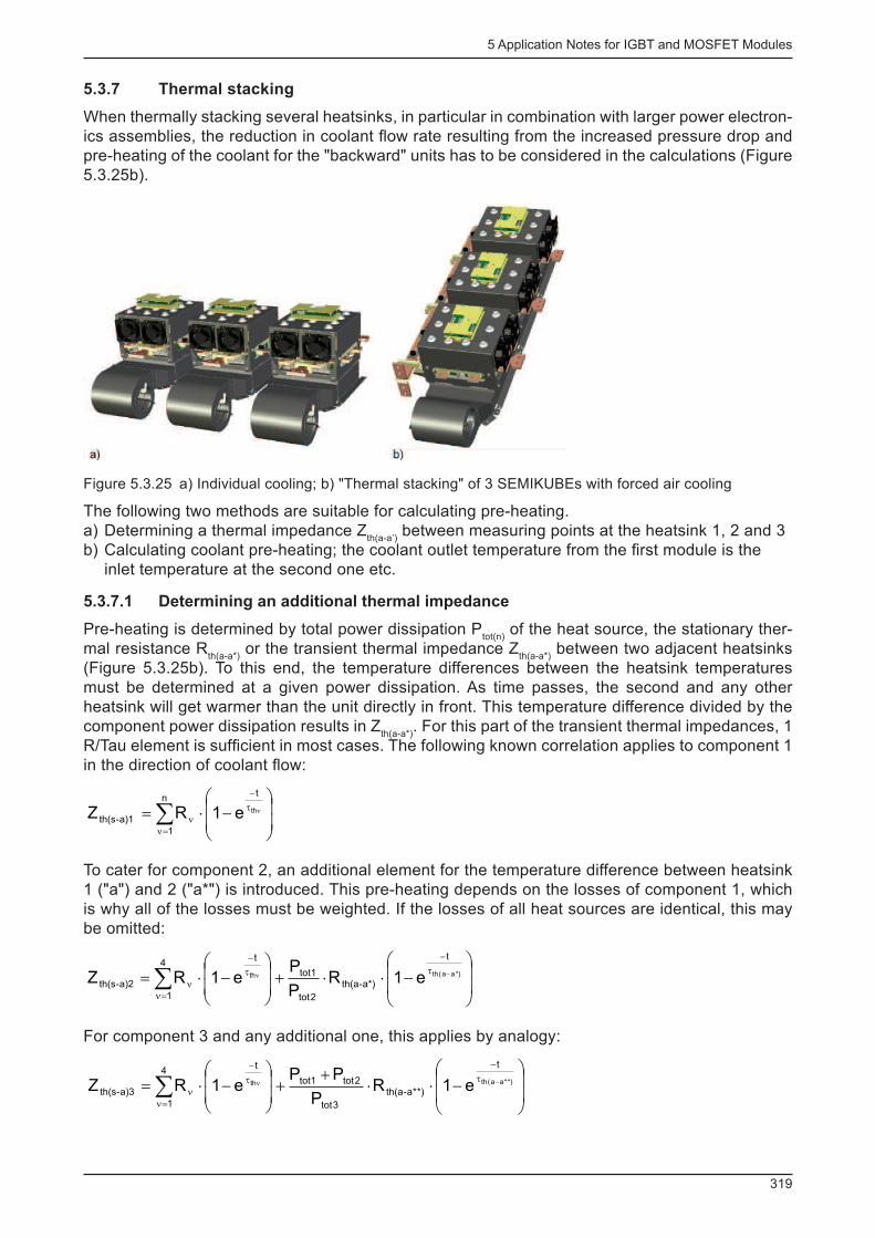
5 Application Notes for IGBT and MOSFET Modules
319
5.3.7 Thermal stacking
When thermally stacking several heatsinks, in particular in combination with larger power electron-ics assemblies, the reduction in coolant fl ow rate resulting from the increased pressure drop and pre-heating of the coolant for the "backward" units has to be considered in the calculations (Figure 5.3.25b).
Figure 5.3.25 a) Individual cooling; b) "Thermal stacking" of 3 SEMIKUBEs with forced air cooling
The following two methods are suitable for calculating pre-heating.a) Determining a thermal impedance Z
th(a-a’) between measuring points at the heatsink 1, 2 and 3
b) Calculating coolant pre-heating; the coolant outlet temperature from the fi rst module is the inlet temperature at the second one etc.
5.3.7.1 Determining an additional thermal impedance
Pre-heating is determined by total power dissipation P tot(n)
of the heat source, the stationary ther-mal resistance R
th(a-a*) or the transient thermal impedance Z
th(a-a*) between two adjacent heatsinks
(Figure 5.3.25b). To this end, the temperature differences between the heatsink temperatures must be determined at a given power dissipation. As time passes, the second and any other heatsink will get warmer than the unit directly in front. This temperature difference divided by the component power dissipation results in Z
th(a-a*) . For this part of the transient thermal impedances, 1
R/Tau element is suffi cient in most cases. The following known correlation applies to component 1 in the direction of coolant fl ow:
å=n
t
-
n ÷÷
ø
ö
çç
è
æ-×= n
n
1
t
a)1-th(sthe1RZ
To cater for component 2, an additional element for the temperature difference between heatsink 1 ("a") and 2 ("a*") is introduced. This pre-heating depends on the losses of component 1, which is why all of the losses must be weighted. If the losses of all heat sources are identical, this may be omitted:
÷÷
ø
ö
çç
è
æ-××+
÷÷
ø
ö
çç
è
æ-×= -n t
-
=n
t
-
nå *)aa(thth
t
a*)-th(a
2tot
1tot4
1
t
a)2-th(s e1RP
Pe1RZ
For component 3 and any additional one, this applies by analogy:
÷÷
ø
ö
çç
è
æ-××
++
÷÷
ø
ö
çç
è
æ-×= -n t
-
=n
t
-
nå *)*aa(thth
t
*)*a-th(a
3tot
2tot1tot4
1
t
a)3-th(s e1RP
PPe1RZ
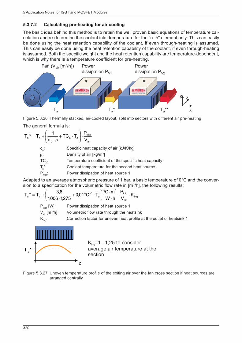
5 Application Notes for IGBT and MOSFET Modules
320
5.3.7.2 Calculating pre-heating for air cooling
The basic idea behind this method is to retain the well proven basic equations of temperature cal-culation and re-determine the coolant inlet temperature for the "n-th" element only: This can easily be done using the heat retention capability of the coolant, if even through-heating is assumed. This can easily be done using the heat retention capability of the coolant, if even through-heating is assumed. Both the specifi c weight and the heat retention capability are temperature-dependent, which is why there is a temperature coeffi cient for pre-heating.
Fan (Vair [m³/h]) Power
dissipation PV1
Ta*Ta
z
x
y
Power
dissipation PV2
Ta**
Figure 5.3.26 Thermally stacked, air-cooled layout, split into sectors with different air pre-heating
The general formula is:
air
1totac
p
aaV
PTTC
c
1T*T ×÷
÷ø
öççè
æ×+
r×+=
c p : Specifi c heat capacity of air [kJ/K/kg]
ρ: Density of air [kg/m³]
TC c : Temperature coeffi cient of the specifi c heat capacity
T a *: Coolant temperature for the second heat source
P tot1
: Power dissipation of heat source 1
Adapted to an average atmospheric pressure of 1 bar, a basic temperature of 0°C and the conver-sion to a specifi cation for the volumetric fl ow rate in [m³/h], the following results:
Ing
air
1tot3
a
1
aa KV
P
hW
mCTC01,0
275,1006,1
6,3T*T ××
××°
÷øö
çèæ ×°+
×+= -
P tot1
[W]: Power dissipation of heat source 1
V air
[m³/h] Volumetric fl ow rate through the heatsink
K ing
: Correction factor for uneven heat profi le at the outlet of heatsink 1
z
Ta*
K =1...1,25 to consider
average air temperature at thesection
Ing
Figure 5.3.27 Uneven temperature profi le of the exiting air over the fan cross section if heat sources are arranged centrally
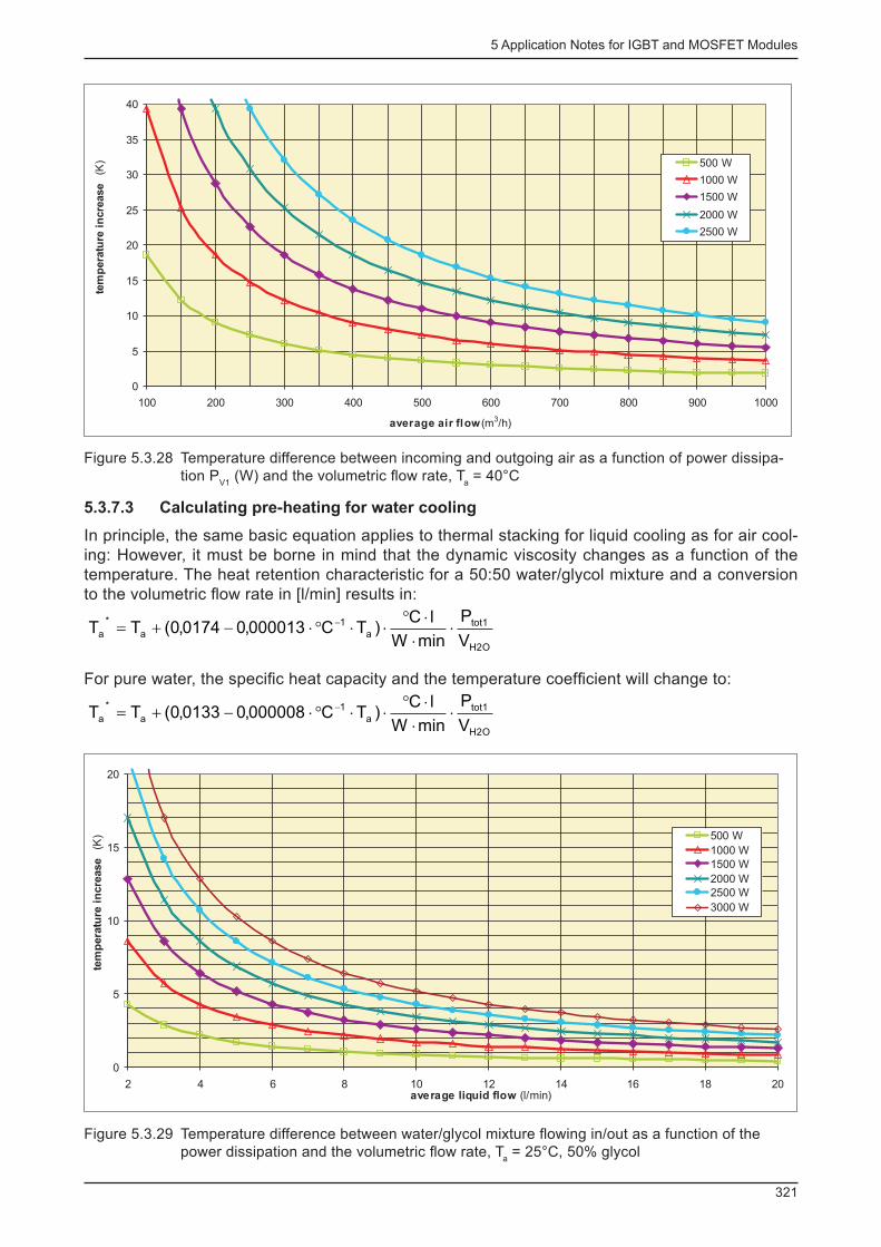
5 Application Notes for IGBT and MOSFET Modules
321
0
5
10
15
20
25
30
35
40
100 200 300 400 500 600 700 800 900 1000
average air flow (m3/h)
tem
pera
ture
incre
ase
(K) 500 W
1000 W
1500 W
2000 W
2500 W
Figure 5.3.28 Temperature difference between incoming and outgoing air as a function of power dissipa-tion P
V1 (W) and the volumetric fl ow rate, T
a = 40°C
5.3.7.3 Calculating pre-heating for water cooling
In principle, the same basic equation applies to thermal stacking for liquid cooling as for air cool-ing: However, it must be borne in mind that the dynamic viscosity changes as a function of the temperature. The heat retention characteristic for a 50:50 water/glycol mixture and a conversion to the volumetric fl ow rate in [l/min] results in:
O2H
1tota
1
a
*
aV
P
minW
lC)TC000013,00174,0(TT ×
××°
××°×-+= -
For pure water, the specifi c heat capacity and the temperature coeffi cient will change to:
O2H
1tota
1
a
*
aV
P
minW
lC)TC000008,00133,0(TT ×
××°
××°×-+= -
29 0,297273890,445860870,594414570,742934990,891422151,03987605 1,1882967 1,336684121,485038321,63335931
30 0,2873669 0,431003670,57460934 0,7181839 0,861727381,005239781,148721111,292171381,43559061
0
5
10
15
20
2 4 6 8 10 12 14 16 18 20average liquid flow (l/min)
tem
pera
ture
incre
ase
(K) 500 W
1000 W
1500 W
2000 W
2500 W
3000 W
Figure 5.3.29 Temperature difference between water/glycol mixture fl owing in/out as a function of the power dissipation and the volumetric fl ow rate, T
a = 25°C, 50% glycol

5 Application Notes for IGBT and MOSFET Modules
322
5.4 Power design, parasitic elements, EMC
Power circuits used to connect power semiconductors and passive components (L, C etc.) are designed in printed circuit board technology, or by means of cables or solid copper or aluminium bars, depending on the currents and voltages to be switched.
Apart from the general specifi cations to be met, for example with regard to creepage and clear-ance distances, current density or heat dissipation, the short switching times within the nano to microsecond range call for a power design which also lives up to the requirements related to high-frequency applications. In this context, commutation circuits are of particular importance, because their parasitic inductive and capacitive characteristics have a crucial infl uence on the overall sys-tem behaviour.
5.4.1 Parasitic inductances and capacitances
To analyse the individual effects of parasitic inductances and capacitances and their interdepend-ence in converters, it suffi ces to examine one commutation circuit.
Figure 5.4.1 shows the commutation circuit of an IGBT converter with parasitic elements, consist-ing of DC link voltage V
d (corresponds to commutation voltage V
K ) and two IGBT switches with
driver and antiparallel freewheeling diodes. The commutation voltage is impressed by the DC link capacitance C
d . The impressed current i
L fl ows out of the commutation circuit.
DriverVRR
Dr
Gon
Goff
±
C11
L21
C41
D1
C31
T1
L61
L31
L41 L51
C21
L71
E`1
DriverVRR
Dr
Gon
Goff
±
C12
L22 D2
C32
T2
L62
L32
L42 L52
C22
L72
E`2
C42
E1
E2L12
L11
Cd
V (V )d K
iL
iK
Figure 5.4.1 Commutation circuit with parasitic inductive and capacitive elements
5 Application Notes for IGBT and MOSFET Modules
323
The effects of parasitic elements/counter-measures
Total commutation circuit inductance
In the commutation circuit with T1 and D2, the sum of L 11
, L 61
, L 31
, L 41
, L 72
, L 52
and L 12
. Similarly, the sum of L
11 , L
71 , L
51 , L
62 , L
32 , L
42 and L
12 is effective in the commutation circuit with D1 and T2.
During active turn-on of T1 or T2, the total commutation inductance becomes effective as turn-on relief, which will reduce turn-on power dissipation in T1 or T2 (cf. chapter 5.9).However, during active turn-off of T1 and T2, as well as during reverse-recovery di/dt of D1 and D2, switching overvoltages are generated in the transistors and diodes due to high di/dt caused by the commutation circuit inductances. This increases turn-off power dissipation and voltage stress in the power semiconductors.This effect is especially critical with regards to short circuits and overload (cf. chapter 5.7). Moreo-ver, undesired high-frequency oscillations in the range of some MHz may be generated in connec-tion with parasitic capacitances.In hard-switching converters, it is therefore vital that inductances in the commutation circuit be reduced to a minimum. With the exception of L
11 and L
12 , all inductances are generated within
the modules and cannot be infl uenced by the user. In this respect, it is up to the manufacturers of power modules to keep on working on the minimisation of internal inductances by improving module assembly technologies (cf. chapter 2.4.).
SEMIKRON datasheets indicate the internal inductances effective at the module output terminals (Example: SKM300GB12T4: L
CE = typ. 15 nH; Example: SEMiX252GB126HDs: L
CE = typ. 18 nH).
In the case of single-switch modules (1 IGBT/MOSFET + 1 inverse diode), the connection of both modules has to be as low-inductive as possible in a converter phase or commutation circuit.
Particularly important here is that the DC link busbars are low-inductive. This applies to the bus-bars between the DC link capacitors, as well as to the connection of the power modules to the DC link. In relation to this, laminated busbar systems (tightly parallelled plate systems) adapted to the specifi c converter layout have become widely accepted in practice, achieving busbar inductances of up to 20...50 nH.
The effect of the remaining inductances L 11
+L 12
on the power semiconductors can still be reduced by connecting C-, RC- or RCD-circuits directly to the DC link terminals of the power modules [AN1]. In most cases, a simple C-circuit with fi lm capacitors within the range of 0.1...2 µF is con-nected. In low-voltage high-current applications, attenuated RC-circuits are preferred.
Emitter / source inductances
The elements L 31
or L 32
of the emitter / source inductances are effective in the power circuit, as well as in the driver circuit of the transistors. Due to the fast di/dt of the transistor current, voltages will be induced that will have the effect of inverse feedback in the driver circuit (emitter / source inverse feedback). This, however, will decelerate the charging process of the gate-emitter capacitance during turn-on or the discharging process of the gate-emitter capacitance during turn-off, result-ing in increased switching times and switching losses. The inverse feedback effect of the emitter may be utilised to limit the collector current di/dt in the case of short circuits near the modules. To minimise the inductances L
31 and L
32 , power modules are equipped with separate emitter control
terminals.
If several BOTTOM driver stages of a converter are supplied by a common operating voltage with negative DC link reference, the parasitic inductances between the ground connectors of the driv-ers and the negative potential of the DC link may cause undesired oscillations in the ground loops. This problem can be solved by way of HF stabilisation of the driver operating voltage near to the output stage or, in high-power converters, by way of separate supply voltage potentials for the BOTTOM driver stages.
Inductances L 21
and L 22
The inductances L 21
or L 22
designate the inductance of the supply line between driver and transis-tor. Apart from increasing the impedance of the driver circuit, they may cause unwelcome oscil-

5 Application Notes for IGBT and MOSFET Modules
324
lations with the input capacitance of the transistor. This may be remedied by using a short, low-inductance connection between driver and transistor. Increasing the gate series resistance may dampen oscillations; this, however, will unintentionally cause an increase in transistor switching losses at the same time. For more details refer to [AN3].
Capacitances
The capacitances C xx
in Figure 5.4.1 stand for the intrinsic capacitances in the power semiconduc-tors (voltage-dependent, non-linear) and cannot be infl uenced by the user. They indicate the mini-mum value for commutation capacitance C
K and, generally speaking, cause a reduction in power
dissipation during turn-off (cf. chapter 1 and chapter 5.9.).Additional power dissipation is generated during active turn-on due to the recharge process of the commutation capacitances; in high-frequency MOSFET applications (...>100 kHz...), in particular, these losses must be taken into account.C
11 and C
12 result in the Miller effect, as well as dynamic dv/dt-feedback to the gate that slows
down the switching process. The circuit must be designed such as to prevent strong capacitive coupling between the inductive supply leads to gate and collector / drain as well as to gate and emitter / source outside the mod-ule, which is likely to cause additional high-frequency parasitic oscillations. This aspect is becom-ing increasingly important in fast high-voltage power MOSFET applications.
5.4.2 EMI and mains feedback
5.4.2.1 Energy processes in converters
The processes that take place in a converter system will always produce unwelcome interference due to the switching of the power semiconductors, on the one hand (Figure 5.4.2), and welcome energy transmission with corresponding signal processing, on the other hand.
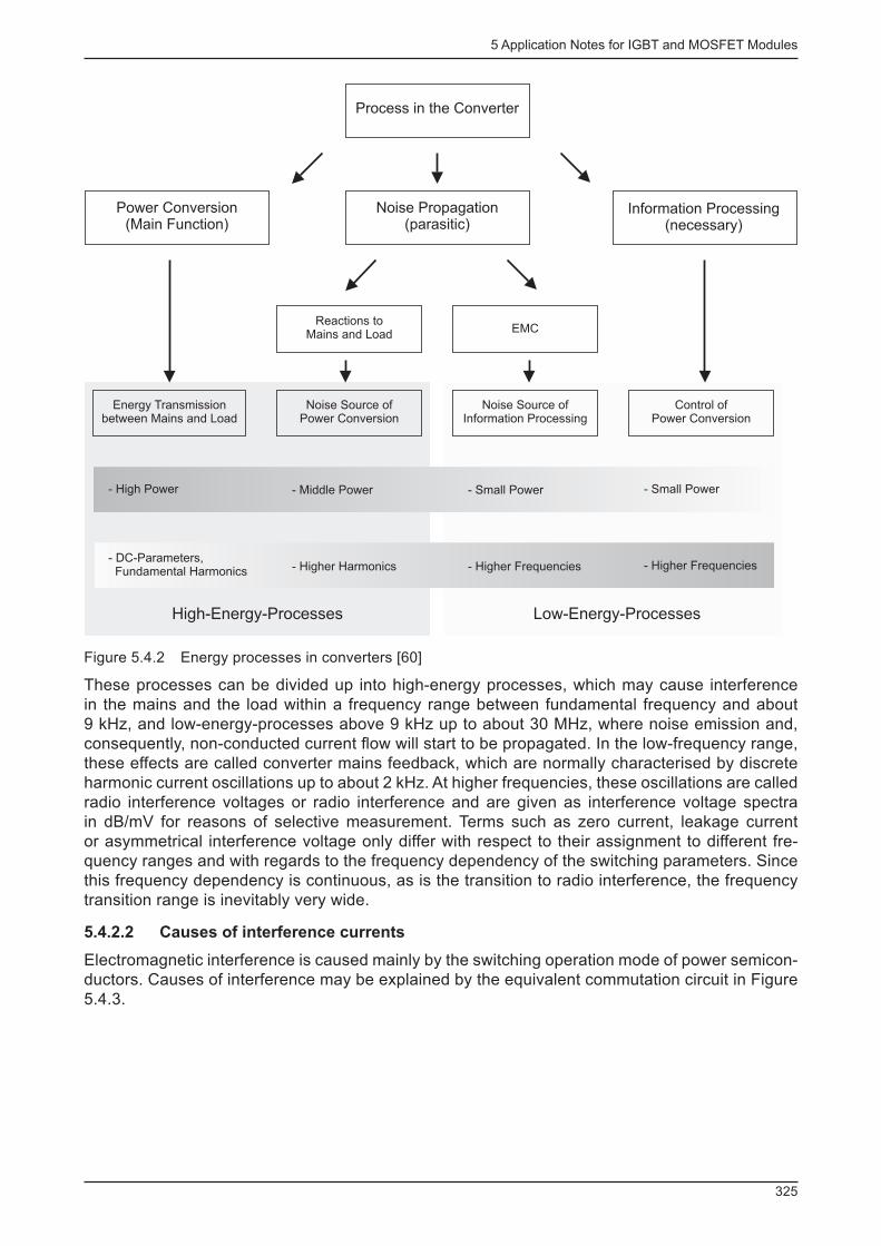
5 Application Notes for IGBT and MOSFET Modules
325
Process in the Converter
Noise Propagation(parasitic)
Power Conversion(Main Function)
Information Processing(necessary)
Reactions toMains and Load
EMC
Energy Transmissionbetween Mains and Load
Noise Source ofPower Conversion
Noise Source ofInformation Processing
Control ofPower Conversion
- High Power - Middle Power - Small Power - Small Power
- DC-Parameters,Fundamental Harmonics - Higher Harmonics - Higher Frequencies - Higher Frequencies
High-Energy-Processes Low-Energy-Processes
Figure 5.4.2 Energy processes in converters [60]
These processes can be divided up into high-energy processes, which may cause interference in the mains and the load within a frequency range between fundamental frequency and about 9 kHz, and low-energy-processes above 9 kHz up to about 30 MHz, where noise emission and, consequently, non-conducted current fl ow will start to be propagated. In the low-frequency range, these effects are called converter mains feedback, which are normally characterised by discrete harmonic current oscillations up to about 2 kHz. At higher frequencies, these oscillations are called radio interference voltages or radio interference and are given as interference voltage spectra in dB/mV for reasons of selective measurement. Terms such as zero current, leakage current or asymmetrical interference voltage only differ with respect to their assignment to different fre-quency ranges and with regards to the frequency dependency of the switching parameters. Since this frequency dependency is continuous, as is the transition to radio interference, the frequency transition range is inevitably very wide.
5.4.2.2 Causes of interference currents
Electromagnetic interference is caused mainly by the switching operation mode of power semicon-ductors. Causes of interference may be explained by the equivalent commutation circuit in Figure 5.4.3.
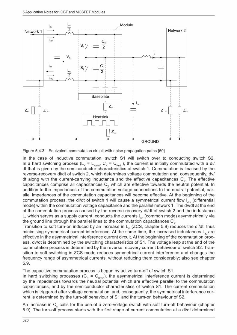
5 Application Notes for IGBT and MOSFET Modules
326
Network 2
Baseplate
VK
Network 1
iL
icm
idm
icm1
idm
icm2
ZN1 Z´N1 Z´N2 ZN2
S1
S2
LK
CK
Module
2
LK
2
2
CK
2
Zch
Zhg
Heatsink
GROUND
Figure 5.4.3 Equivalent commutation circuit with noise propagation paths [60]
In the case of inductive commutation, switch S1 will switch over to conducting switch S2. In a hard switching process (L
K = L
Kmin , C
K = C
Kmin ), the current is initially commutated with a di/
dt that is given by the semiconductor characteristics of switch 1. Commutation is fi nalised by the reverse-recovery di/dt of switch 2, which determines voltage commutation and, consequently, dv/dt along with the current-carrying inductance and the effective capacitances C
K . The effective
capacitances comprise all capacitances C ∑ which are effective towards the neutral potential. In
addition to the impedances of the commutation voltage connections to the neutral potential, par-allel impedances of the commutation capacitances will become effective. At the beginning of the commutation process, the di/dt of switch 1 will cause a symmetrical current fl ow i
dm (differential
mode) within the commutation voltage capacitance and the parallel network 1. The dv/dt at the end of the commutation process caused by the reverse-recovery di/dt of switch 2 and the inductance L, which serves as a supply current, conducts the currents i
cm (common mode) asymmetrically via
the ground line through the parallel lines to the commutation capacitances C K .
Transition to soft turn-on induced by an increase in L K (ZCS, chapter 5.9) reduces the di/dt, thus
minimising symmetrical current interference. At the same time, the increased inductances L K are
effective in the asymmetrical interference current circuit. At the beginning of the commutation proc-ess, dv/dt is determined by the switching characteristics of S1. The voltage leap at the end of the commutation process is determined by the reverse recovery current behaviour of switch S2. Tran-sition to soft switching in ZCS mode reduces symmetrical current interference and changes the frequency range of asymmetrical currents, without reducing them considerably; also see chapter 5.9.
The capacitive commutation process is begun by active turn-off of switch S1.In hard switching processes (C
K = C
Kmin ), the asymmetrical interference current is determined
by the impedances towards the neutral potential which are effective parallel to the commutation capacitances, and by the semiconductor characteristics of switch S1. The current commutation which is triggered after voltage commutation, and, consequently, the symmetrical interference cur-rent is determined by the turn-off behaviour of S1 and the turn-on behaviour of S2.
An increase in C K calls for the use of a zero-voltage switch with soft turn-off behaviour (chapter
5.9). The turn-off process starts with the fi rst stage of current commutation at a di/dt determined
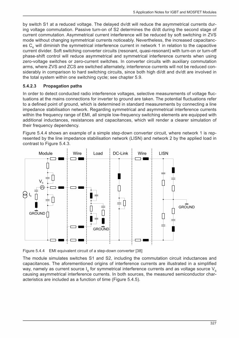
5 Application Notes for IGBT and MOSFET Modules
327
by switch S1 at a reduced voltage. The delayed dv/dt will reduce the asymmetrical currents dur-ing voltage commutation. Passive turn-on of S2 determines the di/dt during the second stage of current commutation. Asymmetrical current interference will be reduced by soft switching in ZVS mode without changing symmetrical currents noticeably. Nevertheless, the increased capacitanc-es C
K will diminish the symmetrical interference current in network 1 in relation to the capacitive
current divider. Soft switching converter circuits (resonant, quasi-resonant) with turn-on or turn-off phase-shift control will reduce asymmetrical and symmetrical interference currents when using zero-voltage switches or zero-current switches. In converter circuits with auxiliary commutation arms, where ZVS and ZCS are switched alternately, interference currents will not be reduced con-siderably in comparison to hard switching circuits, since both high di/dt and dv/dt are involved in the total system within one switching cycle; see chapter 5.9.
5.4.2.3 Propagation paths
In order to detect conducted radio interference voltages, selective measurements of voltage fl uc-tuations at the mains connections for inverter to ground are taken. The potential fl uctuations refer to a defi ned point of ground, which is determined in standard measurements by connecting a line impedance stabilisation network. Regarding symmetrical and asymmetrical interference currents within the frequency range of EMI, all simple low-frequency switching elements are equipped with additional inductances, resistances and capacitances, which will render a clearer simulation of their frequency dependency.
Figure 5.4.4 shows an example of a simple step-down converter circuit, where network 1 is rep-resented by the line impedance stabilisation network (LISN) and network 2 by the applied load in contrast to Figure 5.4.3.
Module Wire Load DC-Link Wire LISN
VS
IS
GROUND
GROUND
GROUND
Figure 5.4.4 EMI equivalent circuit of a step-down converter [38]
The module simulates switches S1 and S2, including the commutation circuit inductances and capacitances. The aforementioned origins of interference currents are illustrated in a simplifi ed way, namely as current source I
S for symmetrical interference currents and as voltage source V
S
causing asymmetrical interference currents. In both sources, the measured semiconductor char-acteristics are included as a function of time (Figure 5.4.5).
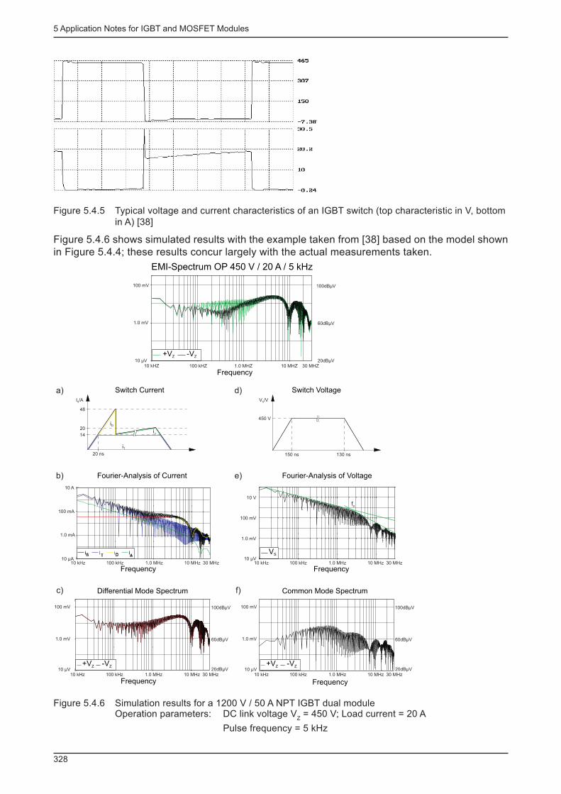
5 Application Notes for IGBT and MOSFET Modules
328
Figure 5.4.5 Typical voltage and current characteristics of an IGBT switch (top characteristic in V, bottom in A) [38]
Figure 5.4.6 shows simulated results with the example taken from [38] based on the model shown in Figure 5.4.4; these results concur largely with the actual measurements taken.
EMI-Spectrum OP 450 V / 20 A / 5 kHz
Frequency
+VZ -VZ
Switch Current Switch Voltage
Fourier-Analysis of Current Fourier-Analysis of Voltage
Frequency Frequency
Differential Mode Spectrum Common Mode Spectrum
Frequency Frequency
VS
+VZ -VZ -VZ+VZ
100 mV
1.0 mV
10 µV10 kHZ 100 kHZ 1.0 MHZ 10 MHZ 30 MHZ
20dBµV
60dBµV
100dBµV
48
20
14
I /AS
a)
b)
20 ns
iD
iT
iD
d)
e)
V /VS
450 V
150 ns 130 ns
10 A
100 mA
1.0 mA
10 µA10 kHz 100 kHz 1.0 MHz 10 MHz 30 MHz 10 kHz 100 kHz 1.0 MHz 10 MHz 30 MHz
10 V
100 mV
1.0 mV
10 µV
fg
100 mV
1.0 mV
10 µV10 kHz 100 kHz 1.0 MHz 10 MHz 30 MHz
100 mV
1.0 mV
10 µV10 kHz 100 kHz 1.0 MHz 10 MHz 30 MHz
20dBµV
60dBµV
100dBµV
20dBµV
60dBµV
100dBµV
c) f)
Figure 5.4.6 Simulation results for a 1200 V / 50 A NPT IGBT dual module Operation parameters: DC link voltage V
Z = 450 V; Load current = 20 A
Pulse frequency = 5 kHz
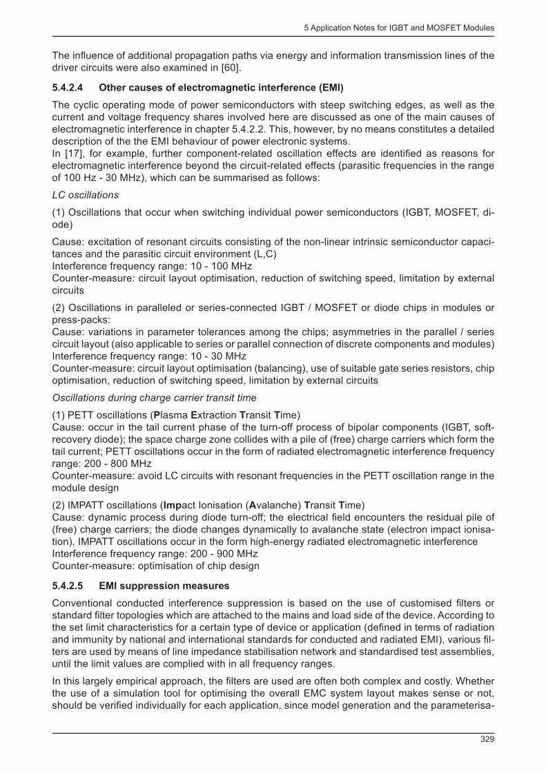
5 Application Notes for IGBT and MOSFET Modules
329
The infl uence of additional propagation paths via energy and information transmission lines of the driver circuits were also examined in [60].
5.4.2.4 Other causes of electromagnetic interference (EMI)
The cyclic operating mode of power semiconductors with steep switching edges, as well as the current and voltage frequency shares involved here are discussed as one of the main causes of electromagnetic interference in chapter 5.4.2.2. This, however, by no means constitutes a detailed description of the the EMI behaviour of power electronic systems. In [17], for example, further component-related oscillation effects are identifi ed as reasons for electromagnetic interference beyond the circuit-related effects (parasitic frequencies in the range of 100 Hz - 30 MHz), which can be summarised as follows:
LC oscillations
(1) Oscillations that occur when switching individual power semiconductors (IGBT, MOSFET, di-ode)
Cause: excitation of resonant circuits consisting of the non-linear intrinsic semiconductor capaci-tances and the parasitic circuit environment (L,C)Interference frequency range: 10 - 100 MHzCounter-measure: circuit layout optimisation, reduction of switching speed, limitation by external circuits
(2) Oscillations in paralleled or series-connected IGBT / MOSFET or diode chips in modules or press-packs:Cause: variations in parameter tolerances among the chips; asymmetries in the parallel / series circuit layout (also applicable to series or parallel connection of discrete components and modules)Interference frequency range: 10 - 30 MHzCounter-measure: circuit layout optimisation (balancing), use of suitable gate series resistors, chip optimisation, reduction of switching speed, limitation by external circuits
Oscillations during charge carrier transit time
(1) PETT oscillations ( P lasma E xtraction T ransit T ime)Cause: occur in the tail current phase of the turn-off process of bipolar components (IGBT, soft-recovery diode); the space charge zone collides with a pile of (free) charge carriers which form the tail current; PETT oscillations occur in the form of radiated electromagnetic interference frequency range: 200 - 800 MHzCounter-measure: avoid LC circuits with resonant frequencies in the PETT oscillation range in the module design
(2) IMPATT oscillations ( Imp act Ionisation ( A valanche) T ransit T ime)Cause: dynamic process during diode turn-off; the electrical fi eld encounters the residual pile of (free) charge carriers; the diode changes dynamically to avalanche state (electron impact ionisa-tion), IMPATT oscillations occur in the form high-energy radiated electromagnetic interferenceInterference frequency range: 200 - 900 MHzCounter-measure: optimisation of chip design
5.4.2.5 EMI suppression measures
Conventional conducted interference suppression is based on the use of customised fi lters or standard fi lter topologies which are attached to the mains and load side of the device. According to the set limit characteristics for a certain type of device or application (defi ned in terms of radiation and immunity by national and international standards for conducted and radiated EMI), various fi l-ters are used by means of line impedance stabilisation network and standardised test assemblies, until the limit values are complied with in all frequency ranges.
In this largely empirical approach, the fi lters are used are often both complex and costly. Whether the use of a simulation tool for optimising the overall EMC system layout makes sense or not, should be verifi ed individually for each application, since model generation and the parameterisa-
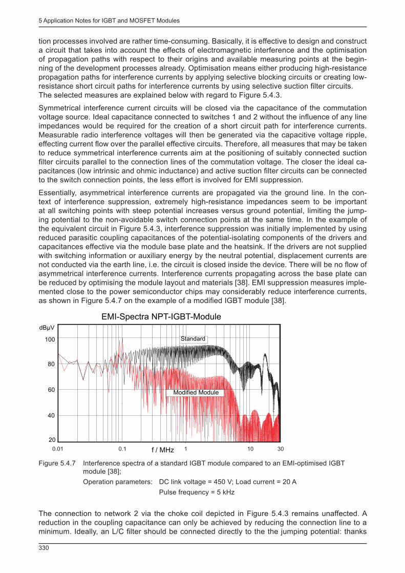
5 Application Notes for IGBT and MOSFET Modules
330
tion processes involved are rather time-consuming. Basically, it is effective to design and construct a circuit that takes into account the effects of electromagnetic interference and the optimisation of propagation paths with respect to their origins and available measuring points at the begin-ning of the development processes already. Optimisation means either producing high-resistance propagation paths for interference currents by applying selective blocking circuits or creating low-resistance short circuit paths for interference currents by using selective suction fi lter circuits. The selected measures are explained below with regard to Figure 5.4.3.
Symmetrical interference current circuits will be closed via the capacitance of the commutation voltage source. Ideal capacitance connected to switches 1 and 2 without the infl uence of any line impedances would be required for the creation of a short circuit path for interference currents. Measurable radio interference voltages will then be generated via the capacitive voltage ripple, effecting current fl ow over the parallel effective circuits. Therefore, all measures that may be taken to reduce symmetrical interference currents aim at the positioning of suitably connected suction fi lter circuits parallel to the connection lines of the commutation voltage. The closer the ideal ca-pacitances (low intrinsic and ohmic inductance) and active suction fi lter circuits can be connected to the switch connection points, the less effort is involved for EMI suppression.
Essentially, asymmetrical interference currents are propagated via the ground line. In the con-text of interference suppression, extremely high-resistance impedances seem to be important at all switching points with steep potential increases versus ground potential, limiting the jump-ing potential to the non-avoidable switch connection points at the same time. In the example of the equivalent circuit in Figure 5.4.3, interference suppression was initially implemented by using reduced parasitic coupling capacitances of the potential-isolating components of the drivers and capacitances effective via the module base plate and the heatsink. If the drivers are not supplied with switching information or auxiliary energy by the neutral potential, displacement currents are not conducted via the earth line, i.e. the circuit is closed inside the device. There will be no fl ow of asymmetrical interference currents. Interference currents propagating across the base plate can be reduced by optimising the module layout and materials [38]. EMI suppression measures imple-mented close to the power semiconductor chips may considerably reduce interference currents, as shown in Figure 5.4.7 on the example of a modifi ed IGBT module [38].
f / MHz
60
20
100
dBµV
80
40
EMI-Spectra NPT-IGBT-Module
Modified Module
Standard
0.01 0.1 1 10 30
Figure 5.4.7 Interference spectra of a standard IGBT module compared to an EMI-optimised IGBT module [38];
Operation parameters: DC link voltage = 450 V; Load current = 20 A
Pulse frequency = 5 kHz
The connection to network 2 via the choke coil depicted in Figure 5.4.3 remains unaffected. A reduction in the coupling capacitance can only be achieved by reducing the connection line to a minimum. Ideally, an L/C fi lter should be connected directly to the the jumping potential: thanks
5 Application Notes for IGBT and MOSFET Modules
331
to the fi lter inductance, potential jumps are attenuated to such an extent that all other coupling capacitances in network 2 will be unable to noticeably contribute to the asymmetrical interference current. Should network 2 serve as the mains supply point where the LISN standard measurement takes place, this step is an absolute must, i.e. the L/C fi lter must be part of the EMI fi lter.
In addition to the use of EMI fi lters, additional measures with respect to earthing and shielding are performed in practice in order to improve EMI behaviour.
5.5 Solutions
5.5.1 Defi nition of the term "solutions"
The terms "solution“ and "SEMISTACK“ are used to designate fully assembled converter power sections such as - line-commutated converter circuits, e.g. B2…B6U/HK/C/CF, W1…W3C, EU - power output stages with IGBT modules, e.g. SEMITRANS, SEMiX, SKiM or SKiiP in customised circuit confi gurations, e.g. B2CI, B6CI, 2xB6CI, step-up and step-down converters as well as combinations thereof.
The functional design usually includes the power semiconductors interconnected in a chassis or case and mounted on heatsinks, the customer interfaces (control and power terminals) and, for IGBT stacks, DC link and snubber capacitors, as well as driver circuits and the necessary poten-tial isolation features. Optionally, fans, temperature and current sensors, protective circuits and semiconductor fusing may be added. Each fully assembled solution undergoes fi nal testing, docu-mented with a test report in some cases.
5.5.2 Platforms
Cost-effective production of solutions is the key to creating competitive advantages for our cus-tomers. To achieve this goal, SEMIKRON has developed a number of platforms based on a modu-lar design concept and the use of identical components where possible. This strategy is crucial in order to achieve short development and qualifi cation times and make optimum use of com-petences. The high-volume effects for components bring about substantial cost advantages for series production as compared with customer-specifi c solutions, enabling short delivery times and an effi cient spare part service at the same time. For this reason, platforms should always be kept in mind when implementing customer projects.

5 Application Notes for IGBT and MOSFET Modules
332
Existing SEMIKRON platforms:
Platform Basic components
Power Semiconductors DC link Cooling
SEMIKUBE SEMITRANS, SEMIPACK Elyt or foil C air*
SEMiXBOX SEMiX Elyt or foil C air*
SKiiPSTACK SKiiP Elyt or foil C air*, water
SEMISTACK Px120 SEMIPACK - air*
SEMISTACK P3 SEMIPACK - air**
SEMISTACK P16 SEMIPACK - air*
SEMISTACK Px308 x) SEMIPACK - air*
SEMISTACK P1 Threaded stud diodes/thyris-tors
- air**
SEMISTACK P 17/18/19, N4
Capsule diodes/thyristors - air*
SEMISTACK P11, U3 Capsule diodes/thyristors air*** x) Structure identical to SEMIKUBE air * : forced air cooling air ** : forced or natural air cooling air *** : natural air cooling
Table 5.5.1 SEMIKRON platforms for solutions
The current Solutions/SEMISTACK product range for the most important platform products (includ-ing datasheets) can be found at www.semikron.com/products. Details on the type designation sys-tem and datasheet content is provided in the "Technical Explanations", likewise accessible online.
5.5.2.1 Platforms with IGBT standard modules
SEMIKUBE
SEMIKUBE B6CI is a fl exible platform for 90...900 kW inverters in B2CI (half-bridge) or B6CI (three-phase inverter) confi guration with an optional rectifi er using standard 62-mm IGBT mod-ules. Figure 5.5.1 shows the functions included and principle layout of a SEMIKUBE module.
Figure 5.5.1 Functions and principle layout of a SEMIKUBE
The SEMIKUBE platforms shown are produced in either inverter, inverter / rectifi er or inverter / bridge arm topology and may be confi gured for even more powerful inverters by varying intercon-nections (Figure 5.5.2).

5 Application Notes for IGBT and MOSFET Modules
333
Figure 5.5.2 SEMIKUBE modular system
Figure 5.5.3 shows SEMIKUBE1 and SEMIKUBE3H assemblies with optional radial fans.
Figure 5.5.3 SEMIKUBE1 and SEMIKUBE3H with optional radial fans
Datasheets and detailed information on the application of SEMIKUBE platforms may be down-loaded at www.semikron.com/products (e.g. [AN2].
SEMiXBOX
SEMiXBOX is a new platform product made by SEMIKRON based on SEMiX IGBT modules fea-turing converter power outputs of 10-90 kW with similar functions to SEMIKUBE.
Figure 5.5.4 shows the main dimensions and module integration options of the 2 different cell sizes (cell3, cell2). As the cells can be connected as desired and cooled using a common fan system, inverter bridges, rectifi ers and chopper circuits can be implemented using SEMiX IGBT, thyristor and diode modules.
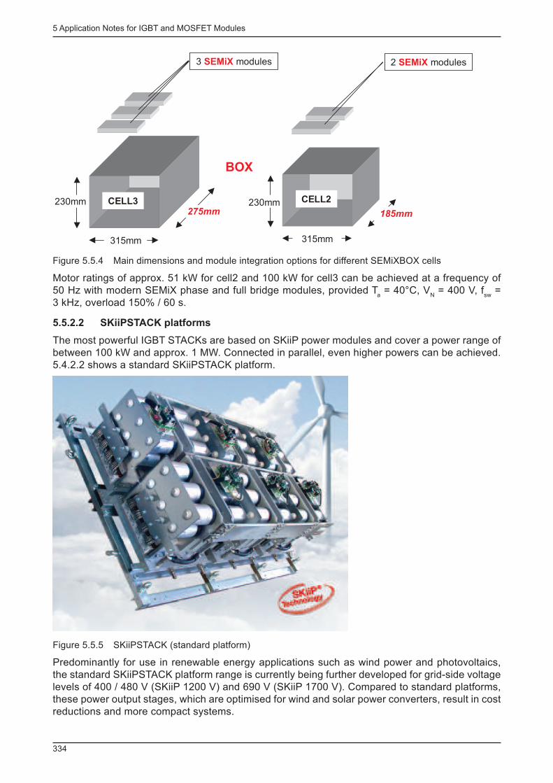
5 Application Notes for IGBT and MOSFET Modules
334
230mm
315mm
275mm
315mm
185mm
BOX
3 SEMiX modules 2 SEMiX modules
CELL3 CELL2230mm
Figure 5.5.4 Main dimensions and module integration options for different SEMiXBOX cells
Motor ratings of approx. 51 kW for cell2 and 100 kW for cell3 can be achieved at a frequency of 50 Hz with modern SEMiX phase and full bridge modules, provided T
a = 40°C, V
N = 400 V, f
sw =
3 kHz, overload 150% / 60 s.
5.5.2.2 SKiiPSTACK platforms
The most powerful IGBT STACKs are based on SKiiP power modules and cover a power range of between 100 kW and approx. 1 MW. Connected in parallel, even higher powers can be achieved. 5.4.2.2 shows a standard SKiiPSTACK platform.
Figure 5.5.5 SKiiPSTACK (standard platform)
Predominantly for use in renewable energy applications such as wind power and photovoltaics, the standard SKiiPSTACK platform range is currently being further developed for grid-side voltage levels of 400 / 480 V (SKiiP 1200 V) and 690 V (SKiiP 1700 V). Compared to standard platforms, these power output stages, which are optimised for wind and solar power converters, result in cost reductions and more compact systems.
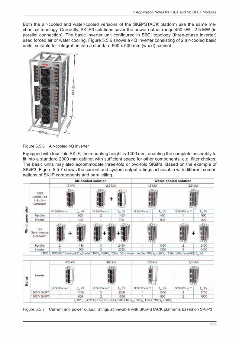
5 Application Notes for IGBT and MOSFET Modules
335
Both the air-cooled and water-cooled versions of the SKiiPSTACK platform use the same me-chanical topology. Currently, SKiiP3 solutions cover the power output range 450 kW…2.5 MW (in parallel connection). The basic inverter unit confi gured in B6CI topology (three-phase inverter) used forced air or water cooling. Figure 5.5.6 shows a 4Q inverter consisting of 2 air-cooled basic units, suitable for integration into a standard 600 x 600 mm (w x d) cabinet.
Figure 5.5.6 Air-cooled 4Q inverter
Equipped with four-fold SKiiP, the mounting height is 1400 mm, enabling the complete assembly to fi t into a standard 2000 mm cabinet with suffi cient space for other components, e.g. fi lter chokes. The basic units may also accommodate three-fold or two-fold SKiiPs. Based on the example of SKiiP3, Figure 5.5.7 shows the current and system output ratings achievable with different combi-nations of SKiiP components and parallelling.
Figure 5.5.7 Current and power output ratings achievable with SKiiPSTACK platforms based on SKiiP3
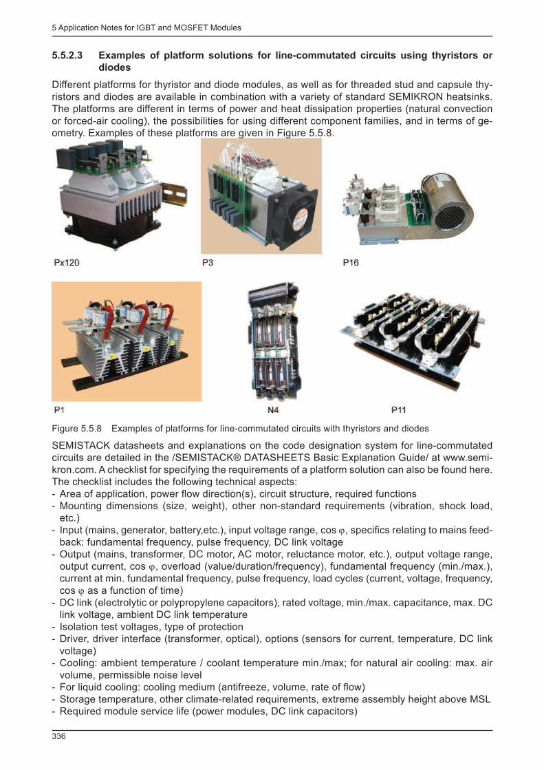
5 Application Notes for IGBT and MOSFET Modules
336
5.5.2.3 Examples of platform solutions for line-commutated circuits using thyristors or
diodes
Different platforms for thyristor and diode modules, as well as for threaded stud and capsule thy-ristors and diodes are available in combination with a variety of standard SEMIKRON heatsinks. The platforms are different in terms of power and heat dissipation properties (natural convection or forced-air cooling), the possibilities for using different component families, and in terms of ge-ometry. Examples of these platforms are given in Figure 5.5.8.
Figure 5.5.8 Examples of platforms for line-commutated circuits with thyristors and diodes
SEMISTACK datasheets and explanations on the code designation system for line-commutated circuits are detailed in the /SEMISTACK® DATASHEETS Basic Explanation Guide/ at www.semi-kron.com. A checklist for specifying the requirements of a platform solution can also be found here. The checklist includes the following technical aspects: - Area of application, power fl ow direction(s), circuit structure, required functions - Mounting dimensions (size, weight), other non-standard requirements (vibration, shock load, etc.)
- Input (mains, generator, battery,etc.), input voltage range, cos ϕ, specifi cs relating to mains feed-back: fundamental frequency, pulse frequency, DC link voltage
- Output (mains, transformer, DC motor, AC motor, reluctance motor, etc.), output voltage range, output current, cos ϕ, overload (value/duration/frequency), fundamental frequency (min./max.), current at min. fundamental frequency, pulse frequency, load cycles (current, voltage, frequency, cos ϕ as a function of time)
- DC link (electrolytic or polypropylene capacitors), rated voltage, min./max. capacitance, max. DC link voltage, ambient DC link temperature
- Isolation test voltages, type of protection - Driver, driver interface (transformer, optical), options (sensors for current, temperature, DC link voltage)
- Cooling: ambient temperature / coolant temperature min./max; for natural air cooling: max. air volume, permissible noise level
- For liquid cooling: cooling medium (antifreeze, volume, rate of fl ow) - Storage temperature, other climate-related requirements, extreme assembly height above MSL - Required module service life (power modules, DC link capacitors)
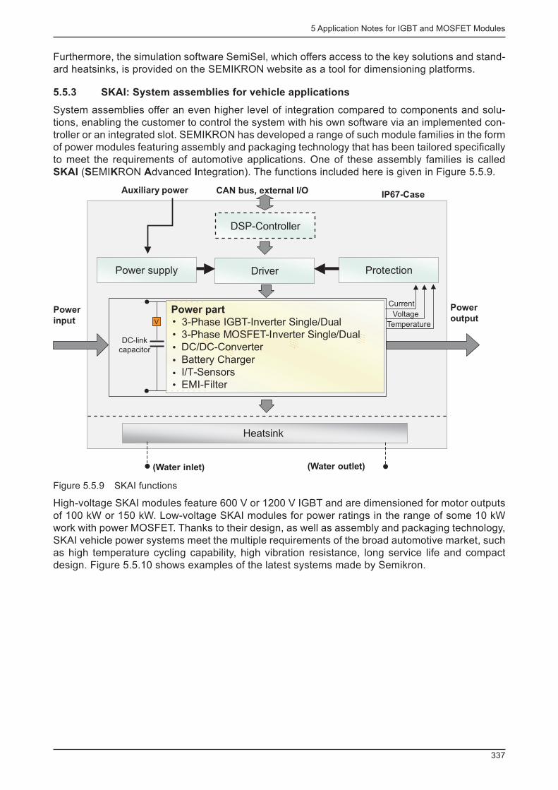
5 Application Notes for IGBT and MOSFET Modules
337
Furthermore, the simulation software SemiSel, which offers access to the key solutions and stand-ard heatsinks, is provided on the SEMIKRON website as a tool for dimensioning platforms.
5.5.3 SKAI: System assemblies for vehicle applications
System assemblies offer an even higher level of integration compared to components and solu-tions, enabling the customer to control the system with his own software via an implemented con-troller or an integrated slot. SEMIKRON has developed a range of such module families in the form of power modules featuring assembly and packaging technology that has been tailored specifi cally to meet the requirements of automotive applications. One of these assembly families is called SKAI ( S EMI K RON A dvanced I ntegration). The functions included here is given in Figure 5.5.9.
Power
output
I
I
V
T
Heatsink
ProtectionDriverPower supply
DSP-Controller
CAN bus, external I/O
Temperature
Voltage
Current
Auxiliary power
Power
input
IP67-Case
DC-link
capacitor
(Water inlet) (Water outlet)
I
Power part
3-Phase IGBT-Inverter Single/Dual
3-Phase MOSFET-Inverter Single/Dual
DC/DC-Converter
Battery Charger
I/T-Sensors
EMI-Filter
Figure 5.5.9 SKAI functions
High-voltage SKAI modules feature 600 V or 1200 V IGBT and are dimensioned for motor outputs of 100 kW or 150 kW. Low-voltage SKAI modules for power ratings in the range of some 10 kW work with power MOSFET. Thanks to their design, as well as assembly and packaging technology, SKAI vehicle power systems meet the multiple requirements of the broad automotive market, such as high temperature cycling capability, high vibration resistance, long service life and compact design. Figure 5.5.10 shows examples of the latest systems made by Semikron.
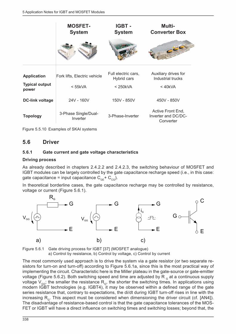
5 Application Notes for IGBT and MOSFET Modules
338
MOSFET-
System
IGBT -
System
Multi-
Converter Box
Application Fork lifts, Electric vehicleFull electric cars,
Hybrid cars
Auxiliary drives for
Industrial trucks
Typical output
power< 55kVA < 250kVA < 40kVA
DC-link voltage 24V - 160V 150V - 850V 450V - 850V
Topology3-Phase Single/Dual-
Inverter3-Phase-Inverter
Active Front End,
Inverter and DC/DC-
Converter
Figure 5.5.10 Examples of SKAI systems
5.6 Driver
5.6.1 Gate current and gate voltage characteristics
Driving process
As already described in chapters 2.4.2.2 and 2.4.2.3, the switching behaviour of MOSFET and IGBT modules can be largely controlled by the gate capacitance recharge speed (i.e., in this case: gate capacitance = input capacitance C
GE + C
CG ).
In theoretical borderline cases, the gate capacitance recharge may be controlled by resistance, voltage or current (Figure 5.6.1).
VGG
iG
VGG
RG
G
E
G
E
G
E
G
E
a) b) c)
C
Figure 5.6.1 Gate driving process for IGBT [37] (MOSFET analogue)a) Control by resistance, b) Control by voltage, c) Control by current
The most commonly used approach is to drive the system via a gate resistor (or two separate re-sistors for turn-on and turn-off) according to Figure 5.6.1a, since this is the most practical way of implementing the circuit. Characteristic here is the Miller plateau in the gate-source or gate-emitter voltage (Figure 5.6.2). Both switching speed and time are adjusted by R
G at a continuous supply
voltage V GG
; the smaller the resistance R G , the shorter the switching times. In applications using
modern IGBT technologies (e.g. IGBT4), it may be observed within a defi ned range of the gate series resistance that, contrary to expectations, the di/dt during IGBT turn-off rises in line with the increasing R
G . This aspect must be considered when dimensioning the driver circuit (cf. [AN4]).
The disadvantage of resistance-based control is that the gate capacitance tolerances of the MOS-FET or IGBT will have a direct infl uence on switching times and switching losses; beyond that, the
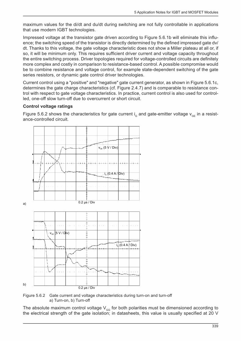
5 Application Notes for IGBT and MOSFET Modules
339
maximum values for the di/dt and du/dt during switching are not fully controllable in applications that use modern IGBT technologies.
Impressed voltage at the transistor gate driven according to Figure 5.6.1b will eliminate this infl u-ence; the switching speed of the transistor is directly determined by the defi ned impressed gate dv/dt. Thanks to this voltage, the gate voltage characteristic does not show a Miller plateau at all or, if so, it will be minimum only. This requires suffi cient driver current and voltage capacity throughout the entire switching process. Driver topologies required for voltage-controlled circuits are defi nitely more complex and costly in comparison to resistance-based control. A possible compromise would be to combine resistance and voltage control, for example state-dependent switching of the gate series resistors, or dynamic gate control driver technologies.
Current control using a "positive" and "negative" gate current generator, as shown in Figure 5.6.1c, determines the gate charge characteristics (cf. Figure 2.4.7) and is comparable to resistance con-trol with respect to gate voltage characteristics. In practice, current control is also used for control-led, one-off slow turn-off due to overcurrent or short circuit.
Control voltage ratings
Figure 5.6.2 shows the characteristics for gate current i G and gate-emitter voltage v
GE in a resist-
ance-controlled circuit.
v (5 V / Div)GE
i (0.4 A / Div)G
0.2 µs / Div
0.2 µs / Div
i (0.4 A / Div)G
v (5 V / Div)GE
a)
b)
Figure 5.6.2 Gate current and voltage characteristics during turn-on and turn-offa) Turn-on, b) Turn-off
The absolute maximum control voltage V GG
for both polarities must be dimensioned according to the electrical strength of the gate isolation; in datasheets, this value is usually specifi ed at 20 V
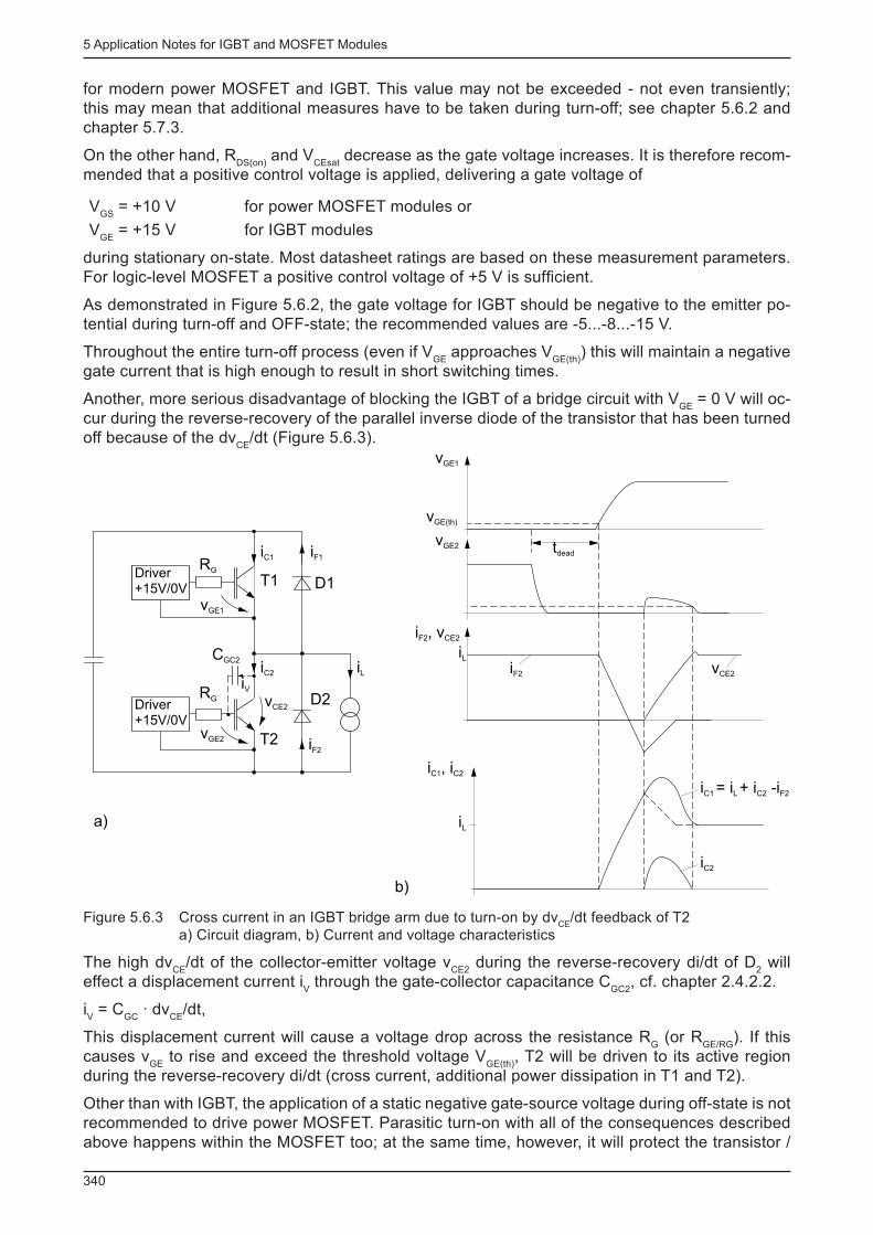
5 Application Notes for IGBT and MOSFET Modules
340
for modern power MOSFET and IGBT. This value may not be exceeded - not even transiently; this may mean that additional measures have to be taken during turn-off; see chapter 5.6.2 and chapter 5.7.3.
On the other hand, R DS(on)
and V CEsat
decrease as the gate voltage increases. It is therefore recom-mended that a positive control voltage is applied, delivering a gate voltage of
V GS
= +10 V for power MOSFET modules or
V GE
= +15 V for IGBT modules
during stationary on-state. Most datasheet ratings are based on these measurement parameters. For logic-level MOSFET a positive control voltage of +5 V is suffi cient.
As demonstrated in Figure 5.6.2, the gate voltage for IGBT should be negative to the emitter po-tential during turn-off and OFF-state; the recommended values are -5...-8...-15 V.
Throughout the entire turn-off process (even if V GE
approaches V GE(th)
) this will maintain a negative gate current that is high enough to result in short switching times.
Another, more serious disadvantage of blocking the IGBT of a bridge circuit with V GE
= 0 V will oc-cur during the reverse-recovery of the parallel inverse diode of the transistor that has been turned off because of the dv
CE /dt (Figure 5.6.3).
iC1
T1
iL
iF2T2
vCE2
iC2
CGC2
iVRG
vGE2
Driver+15V/0V
Driver+15V/0V
RG
vGE1
iC2
i = i + i -iC1 L C2 F2
iL
iL
i , iC1 C2
i , vF2 CE2
iF2 vCE2
tdead
vGE2
vGE(th)
vGE1
iF1
D2
D1
a)
b)
Figure 5.6.3 Cross current in an IGBT bridge arm due to turn-on by dv CE
/dt feedback of T2a) Circuit diagram, b) Current and voltage characteristics
The high dvCE
/dt of the collector-emitter voltage v CE2
during the reverse-recovery di/dt of D 2 will
effect a displacement current i V through the gate-collector capacitance C
GC2 , cf. chapter 2.4.2.2.
i V = C
GC · dv
CE /dt,
This displacement current will cause a voltage drop across the resistance R G (or R
GE/RG ). If this
causes v GE
to rise and exceed the threshold voltage V GE(th)
, T2 will be driven to its active region during the reverse-recovery di/dt (cross current, additional power dissipation in T1 and T2).
Other than with IGBT, the application of a static negative gate-source voltage during off-state is not recommended to drive power MOSFET. Parasitic turn-on with all of the consequences described above happens within the MOSFET too; at the same time, however, it will protect the transistor /
5 Application Notes for IGBT and MOSFET Modules
341
diode structure of the MOSFET, whose dv/dt resistance is limited. The equivalent circuit of a power MOSFET (Figure 2.4.16) demonstrates the displacement current through C
DS to the base of the
parasitic npn-bipolar transistor as a result of dv DS
/dt. If the voltage drop at the lateral p-well resis-tor R
W reaches threshold voltage level, the bipolar transistor will be turned on parasitically, which
may lead to destruction of the MOSFET as a result of power dissipation during periodic operation.
Parasitic turn-on of the MOSFET channel at V GS
= 0 V over C GD
will reduce dv DS
/dt during blocking state and will weaken the unwelcome effect of bipolar transistor turn-on (cf. Figure 5.6.3).
Furthermore, parasitic turn-on of the MOSFET channel will reduce dv/dt at the moment of the body diode's turn-off during reverse recovery, thus avoiding failure of the diode as a consequence of its restricted dynamic ruggedness.
In fi eld applications, MOSFET driver circuits are known which switch towards 0 V during the body diode's commutation process and apply a negative gate voltage during static off-state of the switch.
Control current ratings, driving power
The total driving power P Gavg
to be delivered by the driver circuit can be determined from the gate charge Q
Gtot (cf. Figure 2.4.7):
( ) sGtotGGGGGavg fQVVP ××+= -+ where ( )-+ +×= GGGGERSATZGtot VVCQ
Peak gate current values are calculated as follows:
( ) GonGGGGGMon R/VVI -+ += (ideal)
( ) GoffGGGGGMoff R/VVI -+ += (ideal)
The ideal calculation method neither considers the internal resistance effective in the driver output stage, nor does it take account of the dynamically effective wave impedance resulting from the driver circuit inductance and input capacitance of the IGBT / MOSFET. The smaller the external gate series resistance, the bigger the difference between ideal and real gate peak current.
Driver power per channel is calculated as follows:
( ) sGtotGGGG fQVVP ××= ++ f s = switching frequency
( ) sGtotGGGG fQVVP ××= --
Example: V GG+
= 15 V, V GG-
= -15 V, R
Gint = 2.5 Ω, R
Gon = R
Goff = 1.5 Ω
Q Gtot
= 2.4 µC (SKM300GB12E4)
f s = 10 kHz, V
DC = 600 V
Resulting in:
A5,7II GMoffGMon ==
(ideal)
W72,0PGav =
W36,0)V(P)V(P GGGG == -+
mA24)V(I)V(I GGGG == -+
(average)
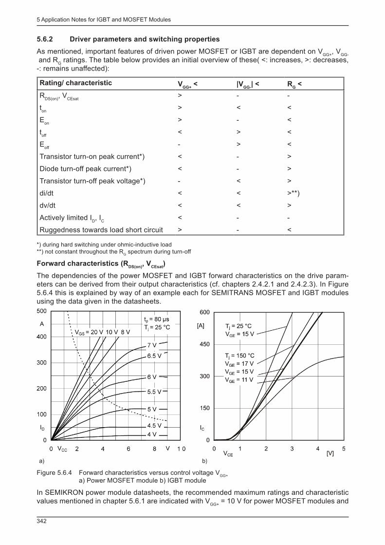
5 Application Notes for IGBT and MOSFET Modules
342
5.6.2 Driver parameters and switching properties
As mentioned, important features of driven power MOSFET or IGBT are dependent on V GG+
, V GG-
and R
G ratings. The table below provides an initial overview of these( <: increases, >: decreases,
-: remains unaffected):
Rating/ characteristic V GG+
< |V GG-
| < R G <
R DS(on)
, V CEsat
t on
E on
t off
E off
Transistor turn-on peak current*)
Diode turn-off peak current*)
Transistor turn-off peak voltage*)
di/dt
dv/dt
Actively limited I D , I
C
Ruggedness towards load short circuit
>
>
>
<
-
<
<
-
<
<
<
>
-
<
-
>
>
-
-
<
<
<
-
-
-
<
<
<
<
>
>
>
>**)
>
-
< *) during hard switching under ohmic-inductive load **) not constant throughout the R
G spectrum during turn-off
Forward characteristics (R DS(on)
, V CEsat
)
The dependencies of the power MOSFET and IGBT forward characteristics on the drive param-eters can be derived from their output characteristics (cf. chapters 2.4.2.1 and 2.4.2.3). In Figure 5.6.4 this is explained by way of an example each for SEMITRANS MOSFET and IGBT modules using the data given in the datasheets.
Figure 5.6.4 Forward characteristics versus control voltage V GG+
a) Power MOSFET module b) IGBT module
In SEMIKRON power module datasheets, the recommended maximum ratings and characteristic values mentioned in chapter 5.6.1 are indicated with V
GG+ = 10 V for power MOSFET modules and
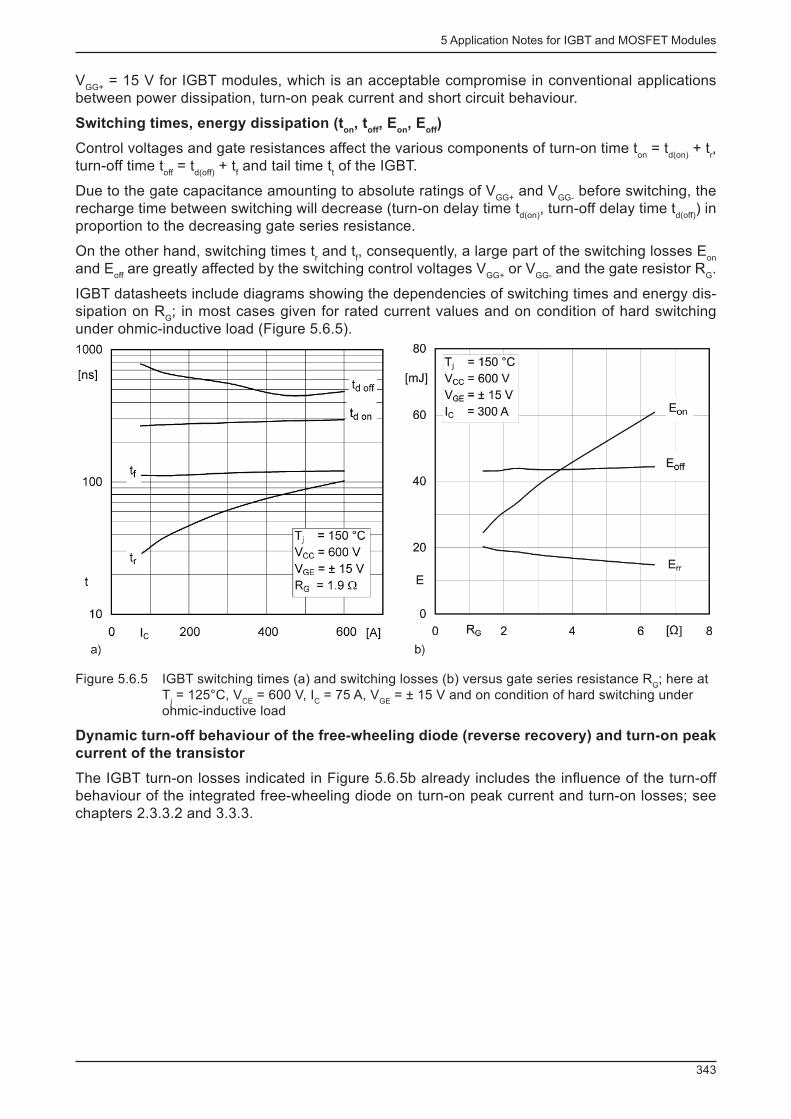
5 Application Notes for IGBT and MOSFET Modules
343
V GG+
= 15 V for IGBT modules, which is an acceptable compromise in conventional applications between power dissipation, turn-on peak current and short circuit behaviour.
Switching times, energy dissipation (t on
, t off
, E on
, E off
)
Control voltages and gate resistances affect the various components of turn-on time t on
= t d(on)
+ t r ,
turn-off time t off
= t d(off)
+ t f and tail time t
t of the IGBT.
Due to the gate capacitance amounting to absolute ratings of V GG+
and V GG-
before switching, the recharge time between switching will decrease (turn-on delay time t
d(on) , turn-off delay time t
d(off) ) in
proportion to the decreasing gate series resistance.
On the other hand, switching times t r and t
f , consequently, a large part of the switching losses E
on
and E off
are greatly affected by the switching control voltages V GG+
or V GG-
and the gate resistor R G .
IGBT datasheets include diagrams showing the dependencies of switching times and energy dis-sipation on R
G ; in most cases given for rated current values and on condition of hard switching
under ohmic-inductive load (Figure 5.6.5).
Figure 5.6.5 IGBT switching times (a) and switching losses (b) versus gate series resistance R G ; here at
T j = 125°C, V
CE = 600 V, I
C = 75 A, V
GE = ± 15 V and on condition of hard switching under
ohmic-inductive load
Dynamic turn-off behaviour of the free-wheeling diode (reverse recovery) and turn-on peak
current of the transistor
The IGBT turn-on losses indicated in Figure 5.6.5b already includes the infl uence of the turn-off behaviour of the integrated free-wheeling diode on turn-on peak current and turn-on losses; see chapters 2.3.3.2 and 3.3.3.
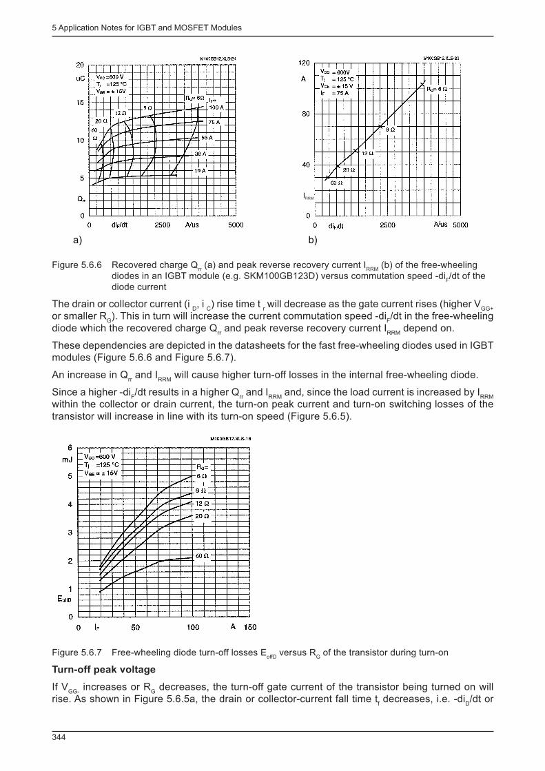
5 Application Notes for IGBT and MOSFET Modules
344
a) b)
IRRM
Figure 5.6.6 Recovered charge Q rr (a) and peak reverse recovery current I
RRM (b) of the free-wheeling
diodes in an IGBT module (e.g. SKM100GB123D) versus commutation speed -di F /dt of the
diode current
The drain or collector current (i D , i
C ) rise time t
r will decrease as the gate current rises (higher V
GG+
or smaller R G ). This in turn will increase the current commutation speed -di
F /dt in the free-wheeling
diode which the recovered charge Q rr and peak reverse recovery current I
RRM depend on.
These dependencies are depicted in the datasheets for the fast free-wheeling diodes used in IGBT modules (Figure 5.6.6 and Figure 5.6.7).
An increase in Q rr and I
RRM will cause higher turn-off losses in the internal free-wheeling diode.
Since a higher -di F /dt results in a higher Q
rr and I
RRM and, since the load current is increased by I
RRM
within the collector or drain current, the turn-on peak current and turn-on switching losses of the transistor will increase in line with its turn-on speed (Figure 5.6.5).
Figure 5.6.7 Free-wheeling diode turn-off losses E offD
versus R G of the transistor during turn-on
Turn-off peak voltage
If V GG-
increases or R G decreases, the turn-off gate current of the transistor being turned on will
rise. As shown in Figure 5.6.5a, the drain or collector-current fall time t f decreases, i.e. -di
D /dt or
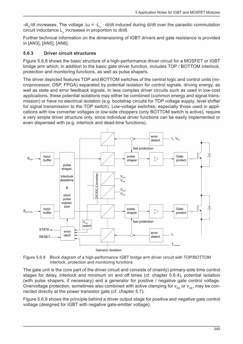
5 Application Notes for IGBT and MOSFET Modules
345
-di C /dt increases. The voltage ∆u = -L
σ · di/dt induced during di/dt over the parasitic commutation
circuit inductance L σ increases in proportion to di/dt.
Further technical information on the dimensioning of IGBT drivers and gate resistance is provided in [AN3], [AN5], [AN6].
5.6.3 Driver circuit structures
Figure 5.6.8 shows the basic structure of a high-performance driver circuit for a MOSFET or IGBT bridge arm which, in addition to the basic gate driver function, includes TOP / BOTTOM interlock, protection and monitoring functions, as well as pulse shapers.
The driver depicted features TOP and BOTTOM switches of the central logic and control units (mi-croprocessor, DSP, FPGA) separated by potential isolation for control signals, driving energy, as well as state and error feedback signals. In less complex driver circuits such as used in low-cost applications, these potential isolations may either be combined (common energy and signal trans-mission) or have no electrical isolation (e.g. bootstrap circuits for TOP voltage supply; level shifter for signal transmission to the TOP switch). Low-voltage switches, especially those used in appli-cations with low converter voltages or low-side choppers (only BOTTOM switch is active), require a very simple driver structure only, since individual driver functions can be easily implemented or even dispensed with (e.g. interlock and dead-time functions).
STOP
inputbuffer
inputbuffer
SBOTTOM
STATE
RESET
errorlatch
pulseshaper,
interlookdeadtime
&
shortpulse
supres-sion
DC
/DC
-Convert
er
VGG+
VGG-
VGG+
VGG-
pulseshaper
fast protection
fast protection
pulseshaper
errordetect.
errordetect.
Gateprotect.
Gateprotect.
IC
I , VC DC
Thmeasur.
Galvanic Isolation
Vwatch
GG
Figure 5.6.8 Block diagram of a high-performance IGBT bridge arm driver circuit with TOP/BOTTOM interlock, protection and monitoring functions
The gate unit is the core part of the driver circuit and consists of (mainly) primary-side time control stages for delay, interlock and minimum on and off times (cf. chapter 5.6.4), potential isolation (with pulse shapers, if necessary) and a generator for positive / negative gate control voltage. Overvoltage protection, sometimes also combined with active clamping for v
DS or v
CE , may be con-
nected directly at the power transistor gate (cf. chapter 5.7).
Figure 5.6.9 shows the principle behind a driver output stage for positive and negative gate control voltage (designed for IGBT with negative gate-emitter voltage).
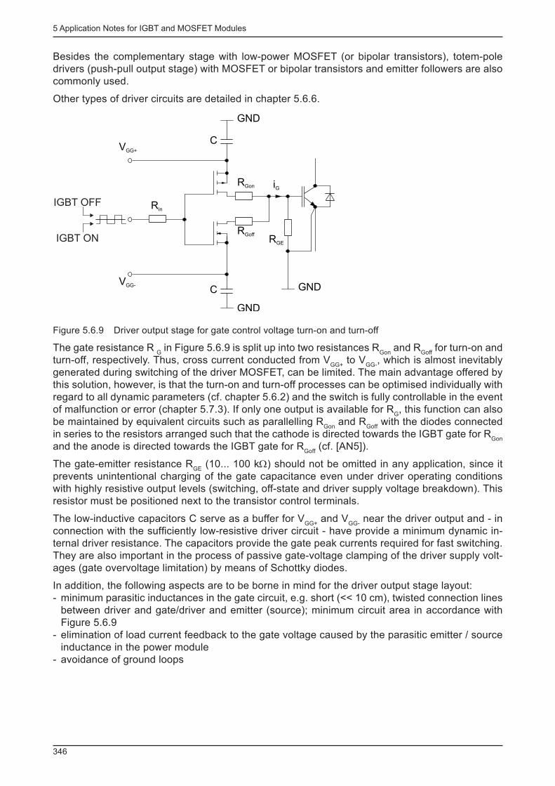
5 Application Notes for IGBT and MOSFET Modules
346
Besides the complementary stage with low-power MOSFET (or bipolar transistors), totem-pole drivers (push-pull output stage) with MOSFET or bipolar transistors and emitter followers are also commonly used.
Other types of driver circuits are detailed in chapter 5.6.6.
GND
VGG+
VGG-
Rin
GND
GND
RGE
RGoff
RGon iG
C
C
IGBT OFF
IGBT ON
Figure 5.6.9 Driver output stage for gate control voltage turn-on and turn-off
The gate resistance R G in Figure 5.6.9 is split up into two resistances R
Gon and R
Goff for turn-on and
turn-off, respectively. Thus, cross current conducted from V GG+
to V GG-
, which is almost inevitably generated during switching of the driver MOSFET, can be limited. The main advantage offered by this solution, however, is that the turn-on and turn-off processes can be optimised individually with regard to all dynamic parameters (cf. chapter 5.6.2) and the switch is fully controllable in the event of malfunction or error (chapter 5.7.3). If only one output is available for R
G , this function can also
be maintained by equivalent circuits such as parallelling R Gon
and R Goff
with the diodes connected in series to the resistors arranged such that the cathode is directed towards the IGBT gate for R
Gon
and the anode is directed towards the IGBT gate for RGoff
(cf. [AN5]).
The gate-emitter resistance R GE
(10... 100 kΩ) should not be omitted in any application, since it prevents unintentional charging of the gate capacitance even under driver operating conditions with highly resistive output levels (switching, off-state and driver supply voltage breakdown). This resistor must be positioned next to the transistor control terminals.
The low-inductive capacitors C serve as a buffer for V GG+
and V GG-
near the driver output and - in connection with the suffi ciently low-resistive driver circuit - have provide a minimum dynamic in-ternal driver resistance. The capacitors provide the gate peak currents required for fast switching. They are also important in the process of passive gate-voltage clamping of the driver supply volt-ages (gate overvoltage limitation) by means of Schottky diodes.
In addition, the following aspects are to be borne in mind for the driver output stage layout: - minimum parasitic inductances in the gate circuit, e.g. short (<< 10 cm), twisted connection lines between driver and gate/driver and emitter (source); minimum circuit area in accordance with Figure 5.6.9
- elimination of load current feedback to the gate voltage caused by the parasitic emitter / source inductance in the power module
- avoidance of ground loops
5 Application Notes for IGBT and MOSFET Modules
347
- avoidance of transformatory and capacitive coupling between gate and collector circuit (oscilla-tion tendency)
For low-pass fi lters, pulse shapers and pulse-width-triggered fl ip-fl ops integrated into the signal transmission paths for interference suppression, their delay times must be able to accommodate the permissible minimum pulse duration and the necessary response times in the event of mal-function / error.
Additional information is provided in [AN3].
5.6.4 Protection and monitoring functions
To protect MOSFET or IGBT modules in the event of malfunction/errors, the use of different ef-fi cient, quick-response protection functions in the driver is recommended, for example overcurrent and short circuit protection, protection from excessive drain-source or collector-emitter voltage, gate overvoltage protection, overtemperature protection and monitoring of the gate control volt-ages V
GG+ and V
GG- .
With reference to Figure 5.6.8, the integration of protective functions in the driver is explained be-low. Realization and dimensioning aspects are dealt with in chapter 5.7.
Overcurrent and short circuit protection
The current signal can be generated as an analogue signal (measured via e.g. shunt, current probe, R
DS(on) of the driven power MOSFET or sense-source / sense-emitter cells) or maximum
rating exceeding (desaturation of the IGBT). As soon as an error has been detected by comparing the actual value to a defi ned maximum rating, an error memory is set (ERROR status) either on switch potential already or - in the case of potential-isolated sensors - in the primary circuit of the driver, which will block the power transistors until the RESET signal is triggered.
If the error memory is integrated on the secondary side, the error memory status signal will be transmitted to the primary side by a potential-isolated unit. If potential-isolating, high-precision cur-rent sensors are used (as for example in SKiiP), their output signal may serve as the actual value for control loops.
Gate overvoltage protection
In contrast to the protection functions described so far, the gate protection might have to limit the gate voltage periodically without the presence of an actual error that would require the power tran-sistors to be turned off. For this reason, there is no connection to the error memory. More details are given in chapter 5.7.3.
Protection from excessive drain-source or collector-emitter voltage
Voltage limitation at the main terminals of a power transistor can be performed by the transistor itself (avalanche-proof MOSFET), by passive networks or by an active circuit, which implements a defi ned partial turn-on of the transistor in case of overvoltage (cf. chapter 5.7.3).
Optional (option "U") basic protection - although this is not able to detect switching peak voltages and other fast overvoltage peaks - which is integrated into the SKiiP driver as static DC bus voltage monitoring is also available. A "quasi"-potential-isolated sensor will indicate the actual DC bus volt-age value, transmit it to the main control circuit in the form of an analogue actual value and set the error memory to ERROR as soon as the limiting value is exceeded. In addition, a brake chopper buffer may be used to protect the DC link capacitors from active feedback loads.

5 Application Notes for IGBT and MOSFET Modules
348
Overtemperature protection
The temperature of the power transistor chips, the temperature around the chips and the heatsink temperature can be determined using the calculation methods described in chapter 5.7.3. If the sensor is isolated, the temperature signal (e.g. voltage) may also be transmitted to a main control circuit. A threshold switch on the primary side will set the error memory to ERROR as soon as a limiting value is exceeded.
Supply undervoltage protection for the gate control voltages V GG+
and V GG-
If the gate control voltage drops considerably, the secondary control, protection and transmission functions may fail. Moreover, this will also mean that the power transistors can no longer be fully controlled or blocked.
In order to detect this critical state in time, either one of the control voltages or the internal driver power supply has to be monitored. In the event of an error or malfunction, the error memory is set to ERROR.
5.6.5 Time constants and interlock functions
Short-pulse suppression
When pulse transformers or opto-couplers are used to isolate the control signal potential, it is par-ticularly important to ensure that the driver is protected from control pulses (interference pulses) which are too low or too short and might cause the driver to malfunction.
Schmitt triggers, for example, can be connected in series to the potential isolation, suppressing all turn-on or turn-off signals lower than logic level (CMOS, TTL) or < 0.2...0.5 ms. A similar solution may be applied to the secondary side of opto-couplers.
Dead-time for bridge arm control and bridge arm short-circuit interlock
To avoid a bridge arm short circuit, MOSFET and IGBT in the same bridge arm must not be switched on at the same time in voltage source circuits.
In the static state, this may be avoided by interlock of both drivers even if the driver input signals are affected by interference (not suitable for current source circuits, because overlapping opera-tion of the drivers would be required).
Depending on the type of transistor, specifi c application and driver, the dead time has to total up to t
dead = 2...8 µs.
The blanking time of short circuit protection featuring measurement of drain or collector
current and drain-source or collector-emitter voltage
If the transistors have to be turned off because one of the limiting values of the given measurement parameters has been exceeded, the turn-on peak current has to be gated from the measurement. When monitoring the desaturation process of an IGBT, the dynamic saturation voltage character-istic has to be considered, too. During the initial microseconds of the turn-on time, V
CEsatdyn is far
higher than its fi nal value V CEsat
(in the static state in accordance with the static forward character-istic) (Figure 5.6.10). For this reason, short circuit protection must be deactivated during transistor turn-on for a minimum blanking time t
min (also referred to as t
bl ) (cf. Figure 5.6.10).
For the sake of safe short circuit suppression (SC-SOA), the blanking time must not exceed the maximum short-circuit time the transistor may be exposed to (typ. 5...10 µs) (cf. chapter 5.7).
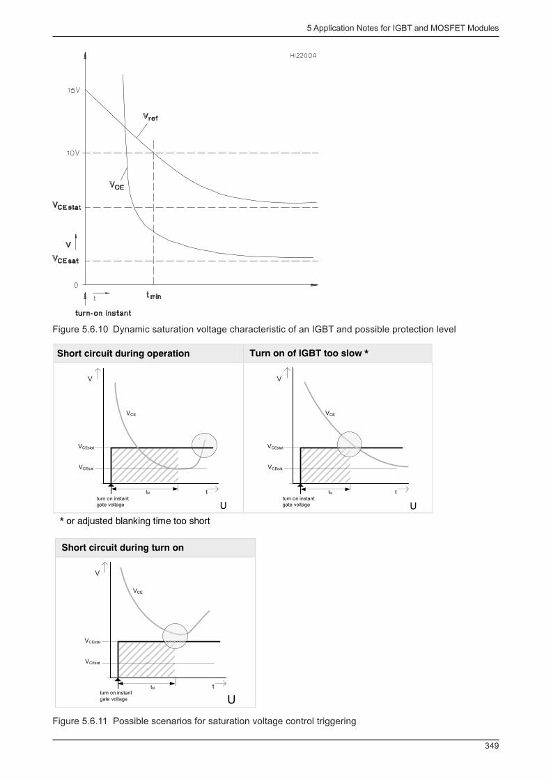
5 Application Notes for IGBT and MOSFET Modules
349
Figure 5.6.10 Dynamic saturation voltage characteristic of an IGBT and possible protection level
Short circuit during operation Turn on of IGBT too slow *
Short circuit during turn on
U
t
VCEstat
VCEsat
VCE
turn on instant
gate voltage
tbl
U
t
VCEstat
VCEsat
VCE
turn on instant
gate voltage
tbl
U
* or adjusted blanking time too short
V V
V
VCE
VCEstat
VCEsat
turn on instant
gate voltage
tbl t
Figure 5.6.11 Possible scenarios for saturation voltage control triggering
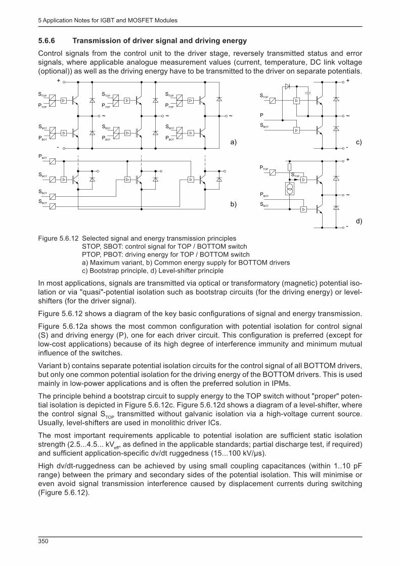
5 Application Notes for IGBT and MOSFET Modules
350
5.6.6 Transmission of driver signal and driving energy
Control signals from the control unit to the driver stage, reversely transmitted status and error signals, where applicable analogue measurement values (current, temperature, DC link voltage (optional)) as well as the driving energy have to be transmitted to the driver on separate potentials.
SBOT
PBOT
STOP
PTOP
SBOT
PBOT
STOP
PTOP
SBOT
PBOT
STOP
PTOP
+
-
~~~
PBOT
SBOT
SBOT
SBOT
~
STOP
SBOT
P
+
-
~
PTOP
SBOT
+
-
PBOT
STOP
a)
b)
c)
d)
Figure 5.6.12 Selected signal and energy transmission principles STOP, SBOT: control signal for TOP / BOTTOM switchPTOP, PBOT: driving energy for TOP / BOTTOM switch a) Maximum variant, b) Common energy supply for BOTTOM driversc) Bootstrap principle, d) Level-shifter principle
In most applications, signals are transmitted via optical or transformatory (magnetic) potential iso-lation or via "quasi"-potential isolation such as bootstrap circuits (for the driving energy) or level-shifters (for the driver signal).
Figure 5.6.12 shows a diagram of the key basic confi gurations of signal and energy transmission.
Figure 5.6.12a shows the most common confi guration with potential isolation for control signal (S) and driving energy (P), one for each driver circuit. This confi guration is preferred (except for low-cost applications) because of its high degree of interference immunity and minimum mutual infl uence of the switches.
Variant b) contains separate potential isolation circuits for the control signal of all BOTTOM drivers, but only one common potential isolation for the driving energy of the BOTTOM drivers. This is used mainly in low-power applications and is often the preferred solution in IPMs.
The principle behind a bootstrap circuit to supply energy to the TOP switch without "proper" poten-tial isolation is depicted in Figure 5.6.12c. Figure 5.6.12d shows a diagram of a level-shifter, where the control signal S
TOP transmitted without galvanic isolation via a high-voltage current source.
Usually, level-shifters are used in monolithic driver ICs.
The most important requirements applicable to potential isolation are suffi cient static isolation strength (2.5...4.5... kV
eff , as defi ned in the applicable standards; partial discharge test, if required)
and suffi cient application-specifi c dv/dt ruggedness (15...100 kV/µs).
High dv/dt-ruggedness can be achieved by using small coupling capacitances (within 1..10 pF range) between the primary and secondary sides of the potential isolation. This will minimise or even avoid signal transmission interference caused by displacement currents during switching (Figure 5.6.12).
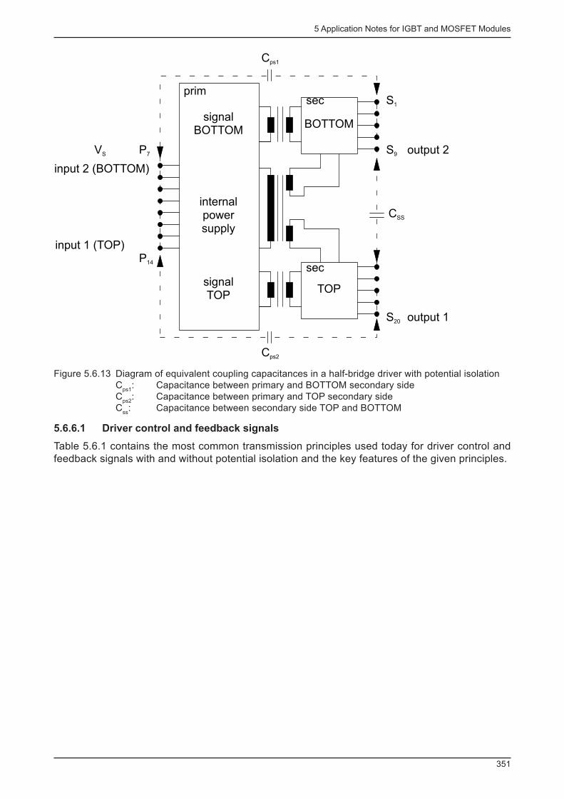
5 Application Notes for IGBT and MOSFET Modules
351
S1
S9 output 2
S20 output 1
CSS
Cps2
Cps1
P7
P14
VS
input 2 (BOTTOM)
prim
signalBOTTOM
internalpowersupply
signalTOP
sec
BOTTOM
TOP
sec
input 1 (TOP)
Figure 5.6.13 Diagram of equivalent coupling capacitances in a half-bridge driver with potential isolationC
ps1 : Capacitance between primary and BOTTOM secondary side
C ps2
: Capacitance between primary and TOP secondary sideC
ss : Capacitance between secondary side TOP and BOTTOM
5.6.6.1 Driver control and feedback signals
Table 5.6.1 contains the most common transmission principles used today for driver control and feedback signals with and without potential isolation and the key features of the given principles.
5 Application Notes for IGBT and MOSFET Modules
352
System
Conventional pulse transformer (with magnetic core)Coreless pulse transformer
Opto-coupler Fibre optic link
Principle behind potential
isolation magnetic
optical/opto-coupler
optical/fi bre optic link
Galvanic isolation yes yes yes
Transmission directions bi-directional uni-directional uni-directional
Inherent delay time
tolerances low high high
Reaction to
magnetic fi eld infl uence + - -
Reaction to
electrical fi eld infl uence - - -
dv/dt immunity (data
taken from datasheet ex-
amples)
35..50..100 kV/µs 15..25 kV/µs n/a
System
Giant Magnetic Resistance (GMR)
transformer
capacitivetransformer
Level shifter
Principle behind
potential isolation magnetic capacitive current source
Galvanic isolation yes yes no
Transmission directions uni-directional uni-directional uni-directional
Inherent delay time
tolerances low low low
Reaction to
magnetic fi eld infl uence + - -
Reaction to
electrical fi eld infl uence - + -
dv/dt immunity (data
taken from datasheet ex-
amples)
..30.. kV/µs 25..50 kV/µs 35..50 kV/µs
Table 5.6.1 Principles behind energy and signal transmission
Analogue output signals may be fed back from the driver to the main control unit in a pulse-width modulated state via potential isolations.
5.6.6.2 Driving energy
Table 5.6.2 gives an overview of the most common solutions used for potential-isolated transmis-sion of driving energy to the driver:

5 Application Notes for IGBT and MOSFET Modules
353
System Mains transformer50 Hz power sup-ply
primary-side DC link side Bootstrap
power supply unit
Principle behind
potential isola-
tion
transformer-coupled (magnetic) blocking pn-junc-tion
Galvanic isola-
tion
yes yes yes no
Supplied by auxiliary voltage or mains voltage
auxiliary voltage DC link operating voltage on BOTTOM side
AC frequency low very high medium medium (pulse fr.)
Smoothing re-
quirements
high very low low low
Output voltage positive and nega-tive
positive and negative positive only
Duty cycle
limitation
no no no yes
Costs - - + - -
Table 5.6.2 Principles behind potential-isolated transmission of driving energy
5.6.7 Monolithic and hybrid driver ICs
In most cases, modern drivers are equipped with monolithical driver ICs which come in a wide variety of single, half-bridge, full-bridge and three-phase bridge driver topologies.
These circuits normally comprise the following functions: - gate voltage generator; - input for V
CEsat - or V
DS(on) monitoring; where applicable input for shunt or sense-emitter, too;
- supply undervoltage monitoring; - error memory and error feedback output; - variable dead time generation; - gate control pulse generation - bootstrap power supply for TOP driver; - shut down input; - integrated level shifters for transmission of TOP driver signals.
Modern monolithical driver ICs are manufactured in latch-up free SOI technology and are char-acterised by their robust level-shifter structures. On the one hand, this results in a considerable improvement in dv/dt-ruggedness. On the other hand, it strengthens the resistance to transient negative voltages and the TOP and BOTTOM driver ground outputs (especially at the TOP-side emitter/source output).
Another possible way to implement an IGBT or MOSFET driver is to combine fast opto-couplers with downstream power driver output stages. Here, to achieve low-cost driver units, all that is needs to be added is a DC/DC converter (or bootstrap circuit) to supply the driving energy, and a few passive components.
With the growing variety of functions and protection mechanisms in driver circuits, the components used in the obligatory primary-side assemblies have to meet ever increasing requirements; these assemblies include, for example, input signal logic, short-pulse suppression, dead time generation, error memory and error evaluation, control for DC/DC converter, and pulse transformer control.
To be able to produce reliable, low-cost driver circuits, these functions have been combined, for instance in control ASICs developed by SEMIKRON.

5 Application Notes for IGBT and MOSFET Modules
354
5.6.8 SEMIDRIVER
SEMIDRIVER are user-friendly, plug-in driver stages for IGBT and MOSFET power modules that differ in the number of driver channels (1, 2, 3, 6 or 7 channels).
By dimensioning the external circuits accordingly, users can adapt the driver parameters, signal interfaces, as well as the protection levels to the given application.
Table 5.6.3 provides an overview of the key parameters of the available driver stages.
Type V CE
[V] V G(on)
[V] V G(off)
[V] I outpeak
[A] Q out/pulse
[µC]
SKHI10/12 R 1200 15 -8 8 9.6
SKHI10/17 R 1700 15 -8 8 9.6
SKHI21 A R 1200 15 0 8 4
SKHI22 A/B H4 R 1700 15 -7 8 4
SKHI22 A/B R 1200 15 -7 8 4
SKHI23/12 R 1200 15 -8 8 4.8
SKHI23/17 R 1700 15 -8 8 4.8
SKHI24 R 1700 15 -8 15 5
SKYPER 32 PRO R 1700 15 -7 15 6.3
SKYPER 32 R 1700 15 -7 15 2.5
SKYPER 52 R 1700 15 -15 50 100
SKHI61 R 900 14.9 -6.5 2 1
SKHI71 R 900 14.9 -6.5 2 1
Type f
max
[kHz]
V iso
[V]
dv/dt
[kV/µs]
Number
of chan-
nels
Supply
voltage
[V]
Input
logic level
[V]
SKHI10/12 R 100 2500 75 1 15 5 or 15
SKHI10/17 R 100 4000 75 1 15 5 or 15
SKHI21 A R 50 2500 50 2 15 15
SKHI22 A/B H4 R 50 4000 50 2 15 15(A), 5(B)
SKHI22 A/B R 50 2500 50 2 15 15(A), 5(B)
SKHI23/12 R 100 2500 75 2 15 5 or 15
SKHI23/17 R 100 4000 75 2 15 5 or 15
SKHI24 R 50 4000 50 2 15 5
SKYPER 32 PRO R 50 4000 50 2 15 15
SKYPER 32 R 50 4000 50 2 15 15
SKYPER 52 R 100 4000 100 2 24 3.3 or 5
SKHI61 R 50 2500 15 6 15 5 or 15
SKHI71 R 50 2500 15 7 15 5 or 15
Table 5.6.3 SEMIDRIVER main parameters
Every SEMIDRIVER includes the following features and functions: - Power supply +15 V on input control signal potential; integrated SMPS with potential isolation - 15 V CMOS and/or 5 V TTL compatible control signal inputs; integrated magnetic pulse trans-

5 Application Notes for IGBT and MOSFET Modules
355
formers for potential isolation - Short circuit protection on the basis of V
CEsat monitoring (reference value at 13 V)
- Driver supply voltage control - Error memory with error feedback and RESET function - Variable dead time (arm interlock time) between driver TOP and BOTTOM for drivers with 2 or more channels
- Short-pulse suppression
Figure 5.6.14 PCB of a SKHI10 driver stage
MONITOR
MEMORY
BUFFER
ERROR
INPUT
VsVs+15V
0V10.11
8.9
Vs
5V
LEVEL
15V
INPUTVin
RESET
ERROR
2
4
3
OUTPUT
BUFFER
IRgoff
- 8V
DC/DCCONVERTER
Vs
+15V
ISOLATION
3
Rgoff
Goff
E2
1
MONITORING
TURN-OFF
SOFT
VCE
J2
RCE CCE
Rgon
SC
Rgoff
VCE
Gon
5
J1
primary side secondary side
1 2
3
4
5
6
7
8
9
10
J3
SELECTOR
1
0W
Figure 5.6.15 Block diagram of a SKHI10 driver stage
SKYPER 32, SKYPER 32 PRO and SKYPER 52 IGBT drivers feature, among others, the following functions: - internal magnetic pulse transformers for potential isolation of control and status signals - internal potential-isolated SMPS for driver supply - Short circuit protection on the basis of V
CEsat monitoring
- Driver supply voltage control - Dead time (arm interlock time) between driver TOP and BOTTOM (not adjustable in SKYPER 32) - Short-pulse suppression - Error management, error inputs and outputs

5 Application Notes for IGBT and MOSFET Modules
356
SKYPER 32 PRO includes the following additional functions: - driver undervoltage protection on primary and secondary side - HALT logic signal - digital parameter setting for arm interlock time - external error input - user-defi nable soft turn-off function in the event of error/malfunction - PCB with protective coating
SKYPER 52 features the following additional functions: - fully digital signal processing - driver undervoltage protection on primary and secondary side - HALT logic signal - common shut down signal - potential-free transmission of temperature signals from TOP to primary side - gate voltage clamping - suppression of input control signal frequencies > 100 kHz - multi-state/progressive turn-off to optimise switching times and switching overvoltages - soft turn-off in the event of error/malfunction - status LEDs - PCB with protective coating
Figure 5.6.16 SKYPER 52 R driver stage PCB
Figure 5.6.17 SKYPER 52 R driver stage block diagram

5 Application Notes for IGBT and MOSFET Modules
357
The "Driver Select Tool“ provided by the simulation and dimensioning software "Semisel“ under www.semikron.com provides the user with a user-friendly aid for selecting the most suitable driver for his application.
5.7 Error behaviour and protection
5.7.1 Types of faults/errors
Power semiconductors have to be protected from non-permissible stress in every operational state. Leaving SOAs leads to damage and, therefore, reduces component life. In the worst case sce-nario, the component will be immediately destroyed. This is why it is important to detect critical states and faults and respond to them with suitable measures.The explanations in this chapter refer mainly to IGBT, but may also be applied to power MOSFET in the same manner. Any matters relevant to MOSFET in particular will be pointed out separately.
Fault currents
Fault currents are collector / drain currents that exceed standard operating values of a certain ap-plication due to control or load errors.They might lead to damage to the power semiconductors due to the following mechanisms: - thermal destruction caused by high power dissipation - dynamic avalanche - static or dynamic latch-up - overvoltages that occur in connection with fault currents
A distinction is made between the following fault currents:
Overcurrent
Features: - usually relatively low collector current di/dt (depending on load inductance and driving voltage) - fault current is conducted through the DC link - transistor does not desaturate
Causes: - reduced load impedance - converter control error
Short-circuit current
Features: - very steep collector current di/dt - fault current is conducted through the DC link - transistor is desaturated
Causes: - arm short circuit (case 1 in Figure 5.7.1)
+ by defective switch + by faulty driver pulses for the switches
- load short circuit (case 2 in Figure 5.7.1) + by faulty isolation + human errors (wrong connection wiring etc.)
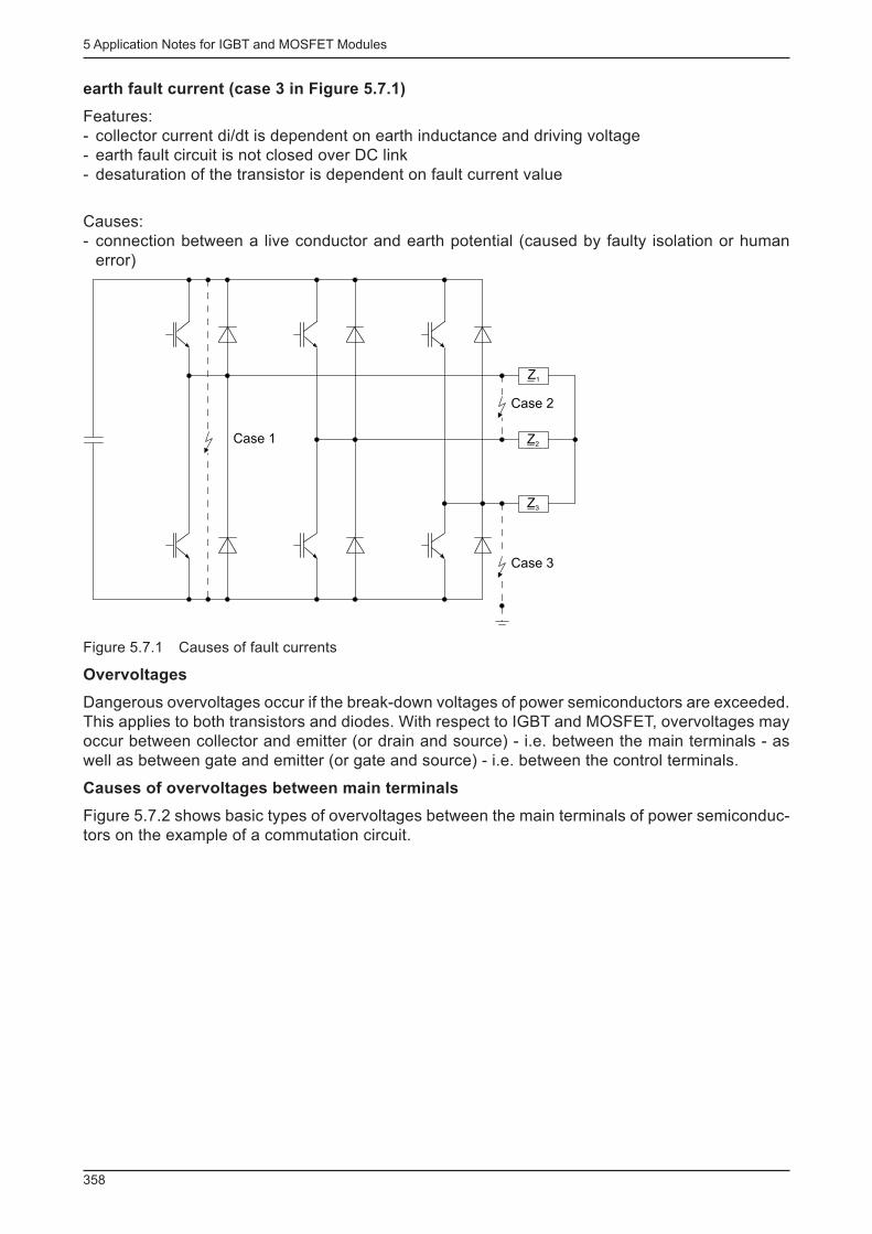
5 Application Notes for IGBT and MOSFET Modules
358
earth fault current (case 3 in Figure 5.7.1)
Features: - collector current di/dt is dependent on earth inductance and driving voltage - earth fault circuit is not closed over DC link - desaturation of the transistor is dependent on fault current value
Causes: - connection between a live conductor and earth potential (caused by faulty isolation or human error)
Z1
Z2
Z3
Case 2
Case 1
Case 3
Figure 5.7.1 Causes of fault currents
Overvoltages
Dangerous overvoltages occur if the break-down voltages of power semiconductors are exceeded. This applies to both transistors and diodes. With respect to IGBT and MOSFET, overvoltages may occur between collector and emitter (or drain and source) - i.e. between the main terminals - as well as between gate and emitter (or gate and source) - i.e. between the control terminals.
Causes of overvoltages between main terminals
Figure 5.7.2 shows basic types of overvoltages between the main terminals of power semiconduc-tors on the example of a commutation circuit.
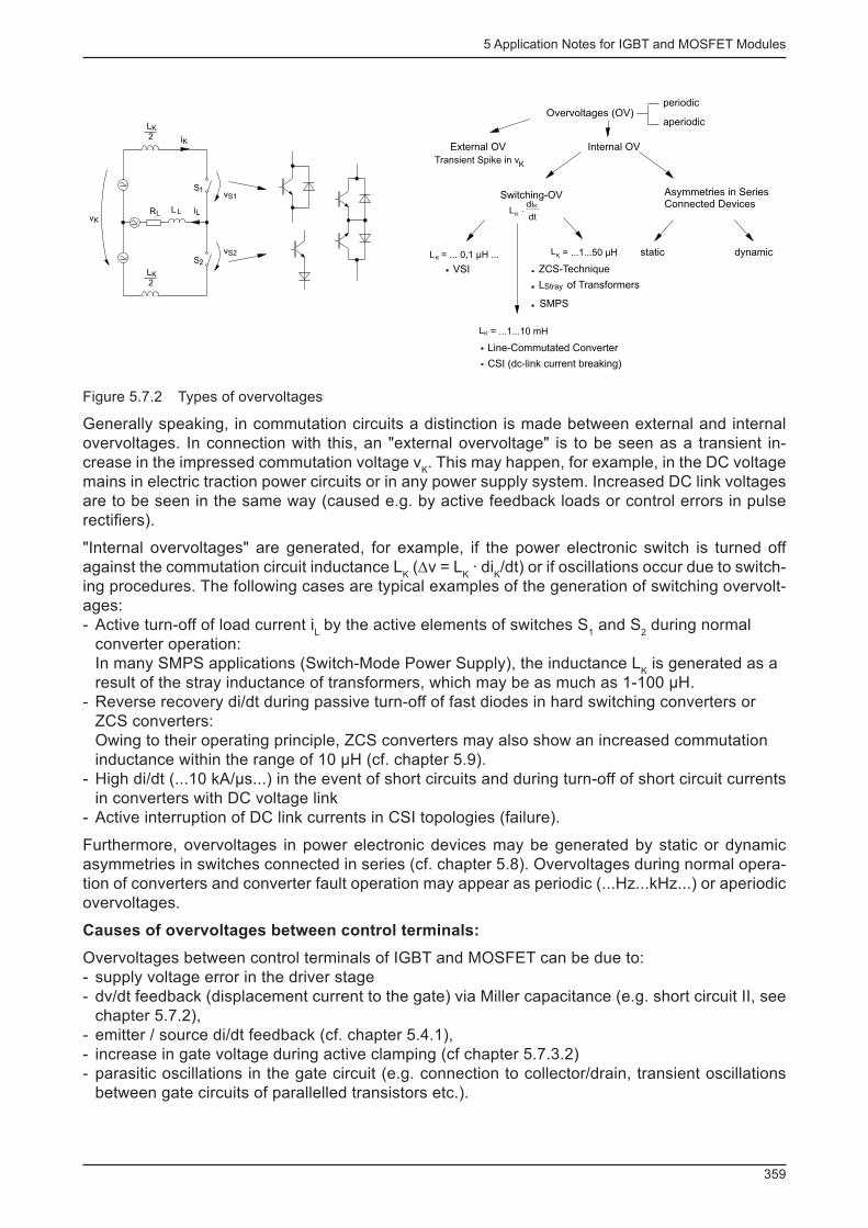
5 Application Notes for IGBT and MOSFET Modules
359
Overvoltages (OV)
External OV Internal OV
Switching-OV Asymmetries in SeriesConnected Devices
static dynamic
periodic
aperiodic
Transient Spike in vK
Ldi
dtK
K
?
LK = ... 0,1 µH ...
VSI
LK = ...1...50 µH
L of TransformersStray
Line-Commutated Converter
LK = ...1...10 mH
CSI (dc-link current breaking)
ZCS-Technique
SMPS
iK
iL
S1
S2
vS1
vS2
vKRL
LK
2
L L
LK
2
Figure 5.7.2 Types of overvoltages
Generally speaking, in commutation circuits a distinction is made between external and internal overvoltages. In connection with this, an "external overvoltage" is to be seen as a transient in-crease in the impressed commutation voltage v
K . This may happen, for example, in the DC voltage
mains in electric traction power circuits or in any power supply system. Increased DC link voltages are to be seen in the same way (caused e.g. by active feedback loads or control errors in pulse rectifi ers).
"Internal overvoltages" are generated, for example, if the power electronic switch is turned off against the commutation circuit inductance L
K (∆v = L
K · di
K /dt) or if oscillations occur due to switch-
ing procedures. The following cases are typical examples of the generation of switching overvolt-ages: - Active turn-off of load current i
L by the active elements of switches S
1 and S
2 during normal
converter operation: In many SMPS applications (Switch-Mode Power Supply), the inductance L
K is generated as a
result of the stray inductance of transformers, which may be as much as 1-100 µH. - Reverse recovery di/dt during passive turn-off of fast diodes in hard switching converters or ZCS converters: Owing to their operating principle, ZCS converters may also show an increased commutation inductance within the range of 10 µH (cf. chapter 5.9).
- High di/dt (...10 kA/µs...) in the event of short circuits and during turn-off of short circuit currents in converters with DC voltage link
- Active interruption of DC link currents in CSI topologies (failure).
Furthermore, overvoltages in power electronic devices may be generated by static or dynamic asymmetries in switches connected in series (cf. chapter 5.8). Overvoltages during normal opera-tion of converters and converter fault operation may appear as periodic (...Hz...kHz...) or aperiodic overvoltages.
Causes of overvoltages between control terminals:
Overvoltages between control terminals of IGBT and MOSFET can be due to: - supply voltage error in the driver stage - dv/dt feedback (displacement current to the gate) via Miller capacitance (e.g. short circuit II, see chapter 5.7.2),
- emitter / source di/dt feedback (cf. chapter 5.4.1), - increase in gate voltage during active clamping (cf chapter 5.7.3.2) - parasitic oscillations in the gate circuit (e.g. connection to collector/drain, transient oscillations between gate circuits of parallelled transistors etc.).
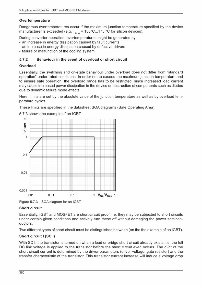
5 Application Notes for IGBT and MOSFET Modules
360
Overtemperature
Dangerous overtemperatures occur if the maximum junction temperature specifi ed by the device manufacturer is exceeded (e.g. T
jmax = 150°C...175 °C for silicon devices).
During converter operation, overtemperatures might be generated by: - an increase in energy dissipation caused by fault currents - an increase in energy dissipation caused by defective drivers - failure or malfunction of the cooling system
5.7.2 Behaviour in the event of overload or short circuit
Overload
Essentially, the switching and on-state behaviour under overload does not differ from "standard operation" under rated conditions. In order not to exceed the maximum junction temperature and to ensure safe operation, the overload range has to be restricted, since increased load current may cause increased power dissipation in the device or destruction of components such as diodes due to dynamic failure mode effects.
Here, limits are set by the absolute value of the junction temperature as well as by overload tem-perature cycles.
These limits are specifi ed in the datasheet SOA diagrams (Safe Operating Area).
5.7.3 shows the example of an IGBT.
0.001
0.01
0.1
1
10
0.001 0.01 0.1 1 10V /VCE CES
I C/I
CR
M
Figure 5.7.3 SOA diagram for an IGBT
Short circuit
Essentially, IGBT and MOSFET are short-circuit proof, i.e. they may be subjected to short circuits under certain given conditions and actively turn these off without damaging the power semicon-ductors.
Two different types of short circuit must be distinguished between (on the the example of an IGBT).
Short circuit I (SC I)
With SC I, the transistor is turned on when a load or bridge short circuit already exists, i.e. the full DC link voltage is applied to the transistor before the short circuit even occurs. The di/dt of the short-circuit current is determined by the driver parameters (driver voltage, gate resistor) and the transfer characteristic of the transistor. This transistor current increase will induce a voltage drop

5 Application Notes for IGBT and MOSFET Modules
361
over the parasitic inductance of the short circuit, which is manifest as a decrease in the collector-emitter voltage characteristic (Figure 5.7.4).
v (500 V / Div)CE
i (200 A / Div)C
v (20 V / Div)GE
1 µs / Div
Figure 5.7.4 SC I characteristics of an IGBT
The static short-circuit current adjusts itself to a value determined by the output characteristic of the transistor. Typical values for IGBT of different technologies are as much as 6...10 fold the rated current (cf. Figure 5.7.7b).
Short circuit II (SC II)
In this case, the transistor is already turned on before the short circuit occurs. Compared to SC I, this case is much more critical with respect to transistor stress.
Figure 5.7.5 shows an equivalent circuit and principle characteristic to explain the SC II proce-dures.
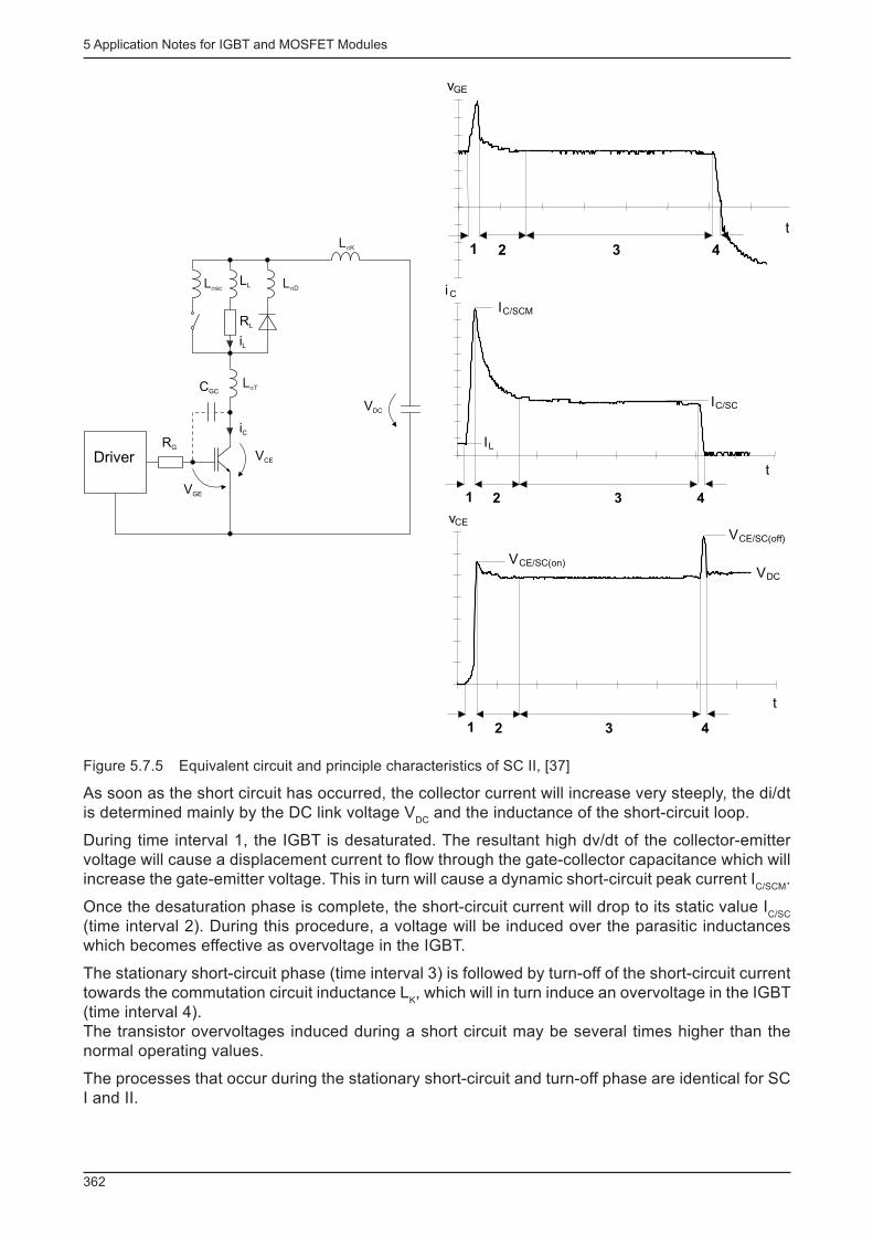
5 Application Notes for IGBT and MOSFET Modules
362
Lssc LsD
LsK
LsT
VGE
LL
iL
iC
DriverRG
VDC
VCE
CGC
RL
vGE
1 2 3 4
t
t
i C
IC/SCM
IC/SC
IL
1 2 3 4
t
vCE
VCE/SC(on)
VCE/SC(off)
VDC
1 2 3 4
Figure 5.7.5 Equivalent circuit and principle characteristics of SC II, [37]
As soon as the short circuit has occurred, the collector current will increase very steeply, the di/dt is determined mainly by the DC link voltage V
DC and the inductance of the short-circuit loop.
During time interval 1, the IGBT is desaturated. The resultant high dv/dt of the collector-emitter voltage will cause a displacement current to fl ow through the gate-collector capacitance which will increase the gate-emitter voltage. This in turn will cause a dynamic short-circuit peak current I
C/SCM .
Once the desaturation phase is complete, the short-circuit current will drop to its static value I C/SC
(time interval 2). During this procedure, a voltage will be induced over the parasitic inductances which becomes effective as overvoltage in the IGBT.
The stationary short-circuit phase (time interval 3) is followed by turn-off of the short-circuit current towards the commutation circuit inductance L
K , which will in turn induce an overvoltage in the IGBT
(time interval 4).The transistor overvoltages induced during a short circuit may be several times higher than the normal operating values.
The processes that occur during the stationary short-circuit and turn-off phase are identical for SC I and II.

5 Application Notes for IGBT and MOSFET Modules
363
VCE 500V/div
IC 400A/div
VGE 20V/div
time 0.5µs/div
dynamic desaturation
Figure 5.7.6 SC II characteristics of an IGBT with external dynamic gate voltage limitation
The SCSOA diagram (SC = short circuit) for short circuit, as shown in the IGBT datasheets or tech-nical explanations, displays the limits for safe control of a short circuit (Figure 5.7.7a).
Figure 5.7.7 Short circuit specifi cations of an IGBTa) SCSOA; non-periodic, parameters: t
sc_max , inductance in the commutation circuit, V
GE , T
jmax
b) short-circuit current normalised to rated current level as a function of the gate-emitter voltage
The following important conditions must be complied with in order to guarantee safe operation under short-circuit conditions: - The short circuit has to be detected and turned off within a defi ned maximum period of time (typi-cally t
sc_max = 10 µs for many technologies).
- The time between two short circuits must be within a defi ned range (typical value for many tech-nologies: 1 s).
- The IGBT must not be subjected to more than a specifi ed maximum number of short circuits dur-ing its entire operating time (typical value for many technologies: 1,000).
Figure 5.7.7b shows the infl uence of gate-emitter voltage and junction temperature on the static short-circuit current.Short circuit I and II cause high losses in the transistor which increase the junction temperature. In such case, the negative temperature coeffi cient of the static short-circuit current, also depicted in the IGBT and MOSFET output characteristic, proves its benefi ts (cf. Figure 5.7.7b).
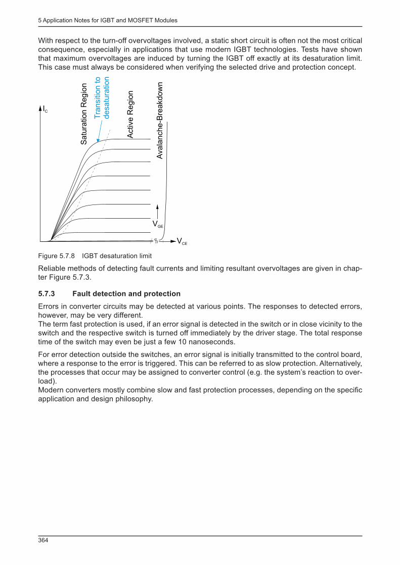
5 Application Notes for IGBT and MOSFET Modules
364
With respect to the turn-off overvoltages involved, a static short circuit is often not the most critical consequence, especially in applications that use modern IGBT technologies. Tests have shown that maximum overvoltages are induced by turning the IGBT off exactly at its desaturation limit. This case must always be considered when verifying the selected drive and protection concept.
Tra
nsitio
n t
od
esa
tura
tio
n
Ava
lan
ch
e-B
rea
kd
ow
n
Sa
tura
tio
n R
eg
ion
Active
Re
gio
n
IC
VGE
VCE
Figure 5.7.8 IGBT desaturation limit
Reliable methods of detecting fault currents and limiting resultant overvoltages are given in chap-ter Figure 5.7.3.
5.7.3 Fault detection and protection
Errors in converter circuits may be detected at various points. The responses to detected errors, however, may be very different.The term fast protection is used, if an error signal is detected in the switch or in close vicinity to the switch and the respective switch is turned off immediately by the driver stage. The total response time of the switch may even be just a few 10 nanoseconds.
For error detection outside the switches, an error signal is initially transmitted to the control board, where a response to the error is triggered. This can be referred to as slow protection. Alternatively, the processes that occur may be assigned to converter control (e.g. the system’s reaction to over-load).Modern converters mostly combine slow and fast protection processes, depending on the specifi c application and design philosophy.
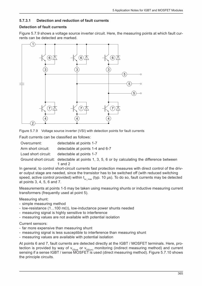
5 Application Notes for IGBT and MOSFET Modules
365
5.7.3.1 Detection and reduction of fault currents
Detection of fault currents
Figure 5.7.9 shows a voltage source inverter circuit. Here, the measuring points at which fault cur-rents can be detected are marked.
5
5
5
3
6
7
4
7
4
7
4
3 3
6 6
2
1
Figure 5.7.9 Voltage source inverter (VSI) with detection points for fault currents
Fault currents can be classifi ed as follows:
Overcurrent: detectable at points 1-7
Arm short circuit: detectable at points 1-4 and 6-7
Load short circuit: detectable at points 1-7
Ground short circuit: detectable at points 1, 3, 5, 6 or by calculating the difference between 1 and 2
In general, to control short-circuit currents fast protection measures with direct control of the driv-er output stage are needed, since the transistor has to be switched off (with reduced switching speed, active control provided) within t
sc_max (typ. 10 µs). To do so, fault currents may be detected
at points 3, 4, 5, 6 and 7.
Measurements at points 1-5 may be taken using measuring shunts or inductive measuring current transformers (frequently used at point 5).
Measuring shunt: - simple measuring method - low-resistance (1...100 mΩ), low-inductance power shunts needed - measuring signal is highly sensitive to interference - measuring values are not available with potential isolation
Current sensors: - far more expensive than measuring shunt - measuring signal is less susceptible to interference than measuring shunt - measuring values are available with potential isolation
At points 6 and 7, fault currents are detected directly at the IGBT / MOSFET terminals. Here, pro-tection is provided by way of v
CEsat or v
DS(on) monitoring (indirect measuring method) and current
sensing if a sense IGBT / sense MOSFET is used (direct measuring method). Figure 5.7.10 shows the principle circuits.
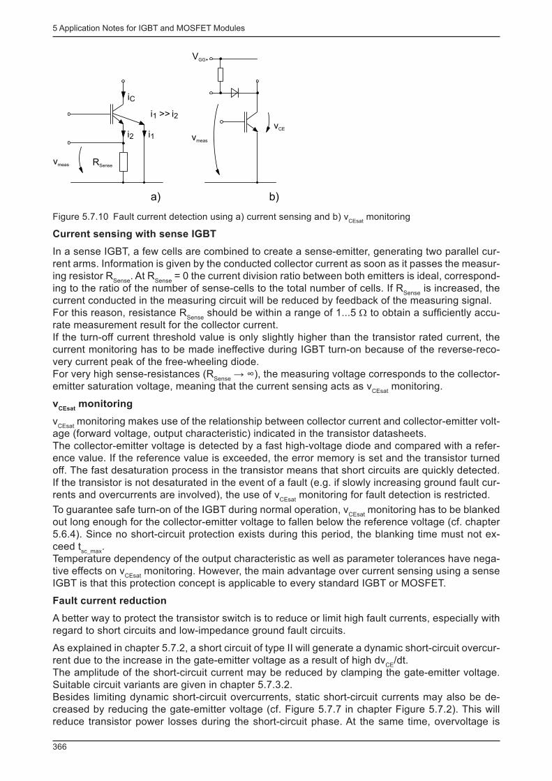
5 Application Notes for IGBT and MOSFET Modules
366
iC
vmeas
i2 i1
RSense
vCE
i1 >> i2
vmeas
a) b)
VGG+
Figure 5.7.10 Fault current detection using a) current sensing and b) v CEsat
monitoring
Current sensing with sense IGBT
In a sense IGBT, a few cells are combined to create a sense-emitter, generating two parallel cur-rent arms. Information is given by the conducted collector current as soon as it passes the measur-ing resistor R
Sense . At R
Sense = 0 the current division ratio between both emitters is ideal, correspond-
ing to the ratio of the number of sense-cells to the total number of cells. If R Sense
is increased, the current conducted in the measuring circuit will be reduced by feedback of the measuring signal.For this reason, resistance R
Sense should be within a range of 1...5 Ω to obtain a suffi ciently accu-
rate measurement result for the collector current.If the turn-off current threshold value is only slightly higher than the transistor rated current, the current monitoring has to be made ineffective during IGBT turn-on because of the reverse-reco-very current peak of the free-wheeling diode.For very high sense-resistances (R
Sense → ∞), the measuring voltage corresponds to the collector-
emitter saturation voltage, meaning that the current sensing acts as v CEsat
monitoring.
v CEsat
monitoring
v CEsat
monitoring makes use of the relationship between collector current and collector-emitter volt-age (forward voltage, output characteristic) indicated in the transistor datasheets.The collector-emitter voltage is detected by a fast high-voltage diode and compared with a refer-ence value. If the reference value is exceeded, the error memory is set and the transistor turned off. The fast desaturation process in the transistor means that short circuits are quickly detected. If the transistor is not desaturated in the event of a fault (e.g. if slowly increasing ground fault cur-rents and overcurrents are involved), the use of v
CEsat monitoring for fault detection is restricted.
To guarantee safe turn-on of the IGBT during normal operation, v CEsat
monitoring has to be blanked out long enough for the collector-emitter voltage to fallen below the reference voltage (cf. chapter 5.6.4). Since no short-circuit protection exists during this period, the blanking time must not ex-ceed t
sc_max .
Temperature dependency of the output characteristic as well as parameter tolerances have nega-tive effects on v
CEsat monitoring. However, the main advantage over current sensing using a sense
IGBT is that this protection concept is applicable to every standard IGBT or MOSFET.
Fault current reduction
A better way to protect the transistor switch is to reduce or limit high fault currents, especially with regard to short circuits and low-impedance ground fault circuits.
As explained in chapter 5.7.2, a short circuit of type II will generate a dynamic short-circuit overcur-rent due to the increase in the gate-emitter voltage as a result of high dv
CE /dt.
The amplitude of the short-circuit current may be reduced by clamping the gate-emitter voltage. Suitable circuit variants are given in chapter 5.7.3.2.Besides limiting dynamic short-circuit overcurrents, static short-circuit currents may also be de-creased by reducing the gate-emitter voltage (cf. Figure 5.7.7 in chapter Figure 5.7.2). This will reduce transistor power losses during the short-circuit phase. At the same time, overvoltage is

5 Application Notes for IGBT and MOSFET Modules
367
decreased, since the short circuit current has to be turned off at a lower level. This principle is shown in Figure 5.7.11.
vDriver
RG
RSense
M1
vCE
iG
iM1
iC
R1
vGE
Figure 5.7.11 Short-circuit current limitation by reducing gate-emitter voltage [37]
This protection method limits the static short-circuit current to about 2.5...3 times the rated current in given applications in practice.
5.7.3.2 Overvoltage limitation
Overvoltage limitation between main terminals [72]
Measures to limit overvoltages between main terminals (collector-emitter voltage, DC link vol-tage) can be divided into passive snubber-networks, active clamping and dynamic gate control.Irrespective of the type of overvoltage limitation, the avalanche operation mode of MOSFET can be utilised, if applicable. The limiting values given in the datasheets must be strictly adhered to. In addition, the suitability of avalanche operation for the intended application should be confi rmed by the manufacturer.
Passive snubber networks
Passive networks (snubbers) are combinations of passive elements such as R, L, C, suppressor diodes, diodes, varistors etc. Figure 5.7.12 shows basic and frequently used circuits.

5 Application Notes for IGBT and MOSFET Modules
368
Basic Circuit
Snubber Variants
a) b) c) d)
Figure 5.7.12 Passive overvoltage limitation networks (snubbers)
Passive snubber networks prevent dangerous overvoltages from being induced by the inductanc-es of the commutation circuit L
K by attaching a capacitor which absorbs the energy stored in L
K (E
= L K /2 · i²). To ensure that the circuit continues to work effectively, the absorbed energy has to be
discharged again between two charging processes. With simple snubbers, this task is performed by heat conversion in the snubber resistors or by feedback to the DC link capacitor.
The simplest method is to clamp the DC link voltage directly to the power module terminals by means of a capacitor (such as a fi lm capacitor). This measure is suffi cient for many VSI applica-tions. In this case, the capacitance value lies in the region of 0.1...2 µF (Figure 5.7.12a).
The following parameters must be considered when dimensioning the capacitor: - DC voltage class of the capacitor (e.g. 1000 V, 1250 V, 1600 V) - Capacitance and minimum parasitic internal inductance - Pulse current capability - Effective capacitor voltage and current (power losses!) - Service life
Figure 5.7.13 shows a simplifi ed equivalent DC link circuit with typical, concentrated parasitic in-ductances.
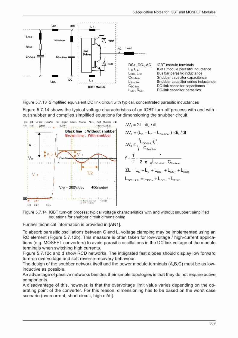
5 Application Notes for IGBT and MOSFET Modules
369
DC+, DC-, AC IGBT module terminalsL C, L E IGBT module parasitic inductanceLDC+, LDC Bus bar parasitic inductanceCSnubber Snubber capacitor capacitanceLSnubber Snubber capacitor series inductanceCDC-link DC-link capacitor capacitanceLESR, RESR DC-link capacitor parasitics
DC+
DC-
AC Load
IGBT Module
IGBT
Driver
L C
L E
LSnubber
LDC+
LDC-
CDC-link
LESR
RESR
CSnubber
TOP
BOT
Figure 5.7.13 Simplifi ed equivalent DC link circuit with typical, concentrated parasitic inductances
Figure 5.7.14 shows the typical voltage characteristics of an IGBT turn-off process with and with-out snubber and compiles simplifi ed equations for dimensioning the snubber circuit.
VCE = 200V/dev 400ns/dev
Vcc
V 3
V 1
Black line : Without snubberBrown line : With snubber
dt/diLV c1 ⋅S=D
dt/di)LLL(V cSnubberEC2 ⋅++=D
Snubber
2
cLinkDC-3
C
iLV
⋅
SnubberLinkDC CL2
1
T
1f
⋅⋅p⋅==
−
ESRDCDCEC LLLLLL ++++=S −+
ESRDCDCLinkDC LLLL ++= −+−
T/2V 1
V 2
D £
Figure 5.7.14 IGBT turn-off process: typical voltage characteristics with and without snubber; simplifi ed equations for snubber circuit dimensioning
Further technical information is provided in [AN1].
To absorb parasitic oscillations between C and L, voltage clamping may be implemented using an RC element (Figure 5.7.12b). This measure is often taken for low-voltage / high-current applica-tions (e.g. MOSFET converters) to avoid parasitic oscillations in the DC link voltage at the module terminals when switching high currents.Figure 5.7.12c and d show RCD networks. The integrated fast diodes should display low forward turn-on overvoltage and soft reverse-recovery behaviour.The design of the snubber network itself and the power module terminals (A,B,C) must be as low-inductive as possible.An advantage of passive networks besides their simple topologies is that they do not require active components.A disadvantage of this, however, is that the overvoltage limit value varies depending on the op-erating point of the converter. For this reason, dimensioning has to be based on the worst case scenario (overcurrent, short circuit, high di/dt).
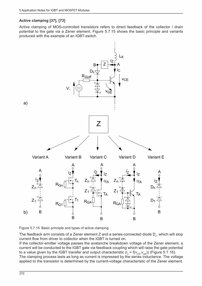
5 Application Notes for IGBT and MOSFET Modules
370
Active clamping [37], [73]
Active clamping of MOS-controlled transistors refers to direct feedback of the collector / drain potential to the gate via a Zener element. Figure 5.7.15 shows the basic principle and variants produced with the example of an IGBT-switch.
iZ
Ds
vCE
vGEV-
RGoff
LK
iC
Z AB
Variant A Variant C Variant D Variant E
Z
iZ
RGn
A
B
RG1
Tn
T1
iZ
A
B
RGA
TA
iZ
Zn
A
B
Z1
iTA
iZ
Zn
Z1
iZ
A
B
RGA
TA
iTA
iZ
Zn
Z1
iZ
Dn
A
B
D1
b)
a)
Variant B
Figure 5.7.15 Basic principle and types of active clamping
The feedback arm consists of a Zener element Z and a series-connected diode D s , which will stop
current fl ow from driver to collector when the IGBT is turned on.If the collector-emitter voltage passes the avalanche breakdown voltage of the Zener element, a current will be conducted to the IGBT gate via feedback coupling which will raise the gate potential to a value given by the IGBT transfer and output characteristic (i
c = f(v
CE ,v
GE )) (Figure 5.7.16).
The clamping process lasts as long as current is impressed by the series inductance. The voltage applied to the transistor is determined by the current-voltage characteristic of the Zener element.
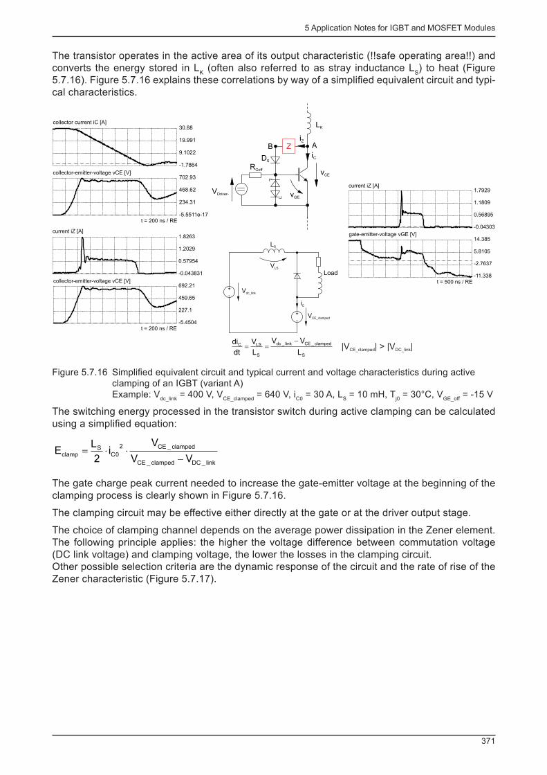
5 Application Notes for IGBT and MOSFET Modules
371
The transistor operates in the active area of its output characteristic (!!safe operating area!!) and converts the energy stored in L
K (often also referred to as stray inductance L
S ) to heat (Figure
5.7.16). Figure 5.7.16 explains these correlations by way of a simplifi ed equivalent circuit and typi-cal characteristics.
+
-
+
-
Vdc_link
LS
VCE_clamped
iC
LoadVLS
S
clamped_CElink_dc
S
LSC
L
VV
L
V
dt
di -==
iZ
DS
vCE
vGE
VDriver-
RGoff
LK
iC
Z AB
collector current iC [A]
collector-emitter-voltage vCE [V]
t = 200 ns / RE
30.88
19.991
9.1022
-1.7864
702.93
468.62
234.31
current iZ [A]
collector-emitter-voltage vCE [V]
1.8263
1.2029
0.57954
-0.043831
692.21
459.65
227.1
-5.4504t = 200 ns / RE
current iZ [A]
gate-emitter-voltage vGE [V]
t = 500 ns / RE
1.7929
1.1809
0.56895
-0.04303
14.385
5.8105
-2.7637
-11.338
-5.5511e-17
|V | > |V |CE_clamped DC_link
Figure 5.7.16 Simplifi ed equivalent circuit and typical current and voltage characteristics during active clamping of an IGBT (variant A)Example: V
dc_link = 400 V, V
CE_clamped = 640 V, i
C0 = 30 A, L
S = 10 mH, T
j0 = 30°C, V
GE_off = -15 V
The switching energy processed in the transistor switch during active clamping can be calculated using a simplifi ed equation:
link_DCclamped_CE
clamped_CE2
0CS
clampVV
Vi
2
LE
-××=
The gate charge peak current needed to increase the gate-emitter voltage at the beginning of the clamping process is clearly shown in Figure 5.7.16.
The clamping circuit may be effective either directly at the gate or at the driver output stage.
The choice of clamping channel depends on the average power dissipation in the Zener element. The following principle applies: the higher the voltage difference between commutation voltage (DC link voltage) and clamping voltage, the lower the losses in the clamping circuit. Other possible selection criteria are the dynamic response of the circuit and the rate of rise of the Zener characteristic (Figure 5.7.17).
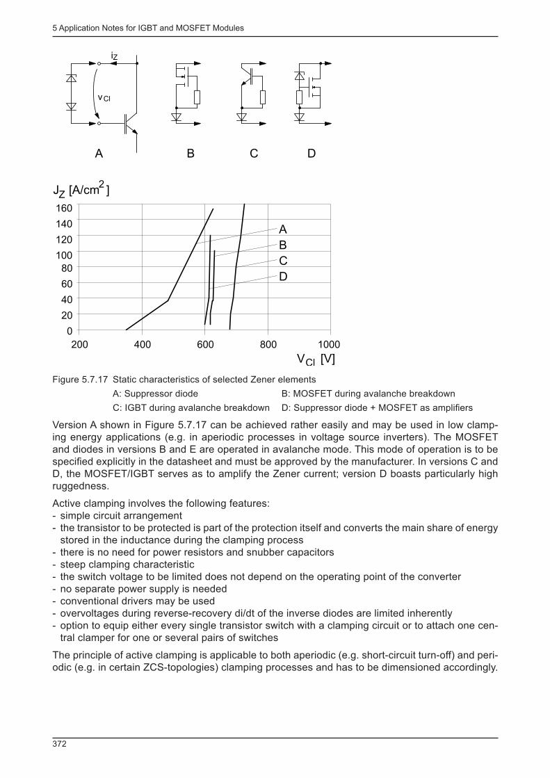
5 Application Notes for IGBT and MOSFET Modules
372
A C D
iZ
vCl
B
A
B
C
D
160
140
120
100
80
60
40
20
0
200 400 600 800 1000
ZJ [A/cm ]2
ClV [V]
Figure 5.7.17 Static characteristics of selected Zener elements
A: Suppressor diode B: MOSFET during avalanche breakdown
C: IGBT during avalanche breakdown D: Suppressor diode + MOSFET as amplifi ers
Version A shown in Figure 5.7.17 can be achieved rather easily and may be used in low clamp-ing energy applications (e.g. in aperiodic processes in voltage source inverters). The MOSFET and diodes in versions B and E are operated in avalanche mode. This mode of operation is to be specifi ed explicitly in the datasheet and must be approved by the manufacturer. In versions C and D, the MOSFET/IGBT serves as to amplify the Zener current; version D boasts particularly high ruggedness.
Active clamping involves the following features: - simple circuit arrangement - the transistor to be protected is part of the protection itself and converts the main share of energy stored in the inductance during the clamping process
- there is no need for power resistors and snubber capacitors - steep clamping characteristic - the switch voltage to be limited does not depend on the operating point of the converter - no separate power supply is needed - conventional drivers may be used - overvoltages during reverse-recovery di/dt of the inverse diodes are limited inherently - option to equip either every single transistor switch with a clamping circuit or to attach one cen-tral clamper for one or several pairs of switches
The principle of active clamping is applicable to both aperiodic (e.g. short-circuit turn-off) and peri-odic (e.g. in certain ZCS-topologies) clamping processes and has to be dimensioned accordingly.
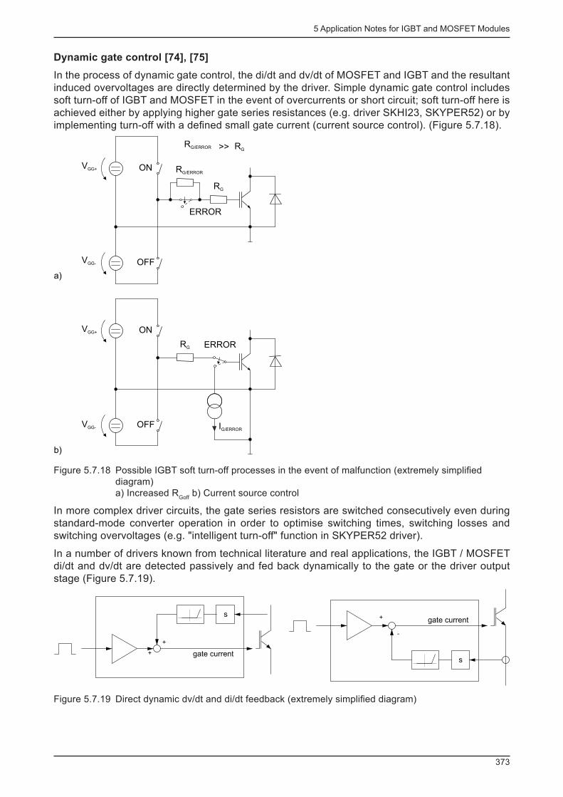
5 Application Notes for IGBT and MOSFET Modules
373
Dynamic gate control [74], [75]
In the process of dynamic gate control, the di/dt and dv/dt of MOSFET and IGBT and the resultant induced overvoltages are directly determined by the driver. Simple dynamic gate control includes soft turn-off of IGBT and MOSFET in the event of overcurrents or short circuit; soft turn-off here is achieved either by applying higher gate series resistances (e.g. driver SKHI23, SKYPER52) or by implementing turn-off with a defi ned small gate current (current source control). (Figure 5.7.18).
VGG+
RG
ON
OFF
ERROR
RG/ERROR
RG/ERROR RG>>
a)
RG
ON
OFF
ERROR
b)
IG/ERROR
VGG-
VGG+
VGG-
Figure 5.7.18 Possible IGBT soft turn-off processes in the event of malfunction (extremely simplifi ed diagram)a) Increased R
Goff b) Current source control
In more complex driver circuits, the gate series resistors are switched consecutively even during standard-mode converter operation in order to optimise switching times, switching losses and switching overvoltages (e.g. "intelligent turn-off" function in SKYPER52 driver).
In a number of drivers known from technical literature and real applications, the IGBT / MOSFET di/dt and dv/dt are detected passively and fed back dynamically to the gate or the driver output stage (Figure 5.7.19).
gate current
sgate current
s
+
+
-
+
Figure 5.7.19 Direct dynamic dv/dt and di/dt feedback (extremely simplifi ed diagram)
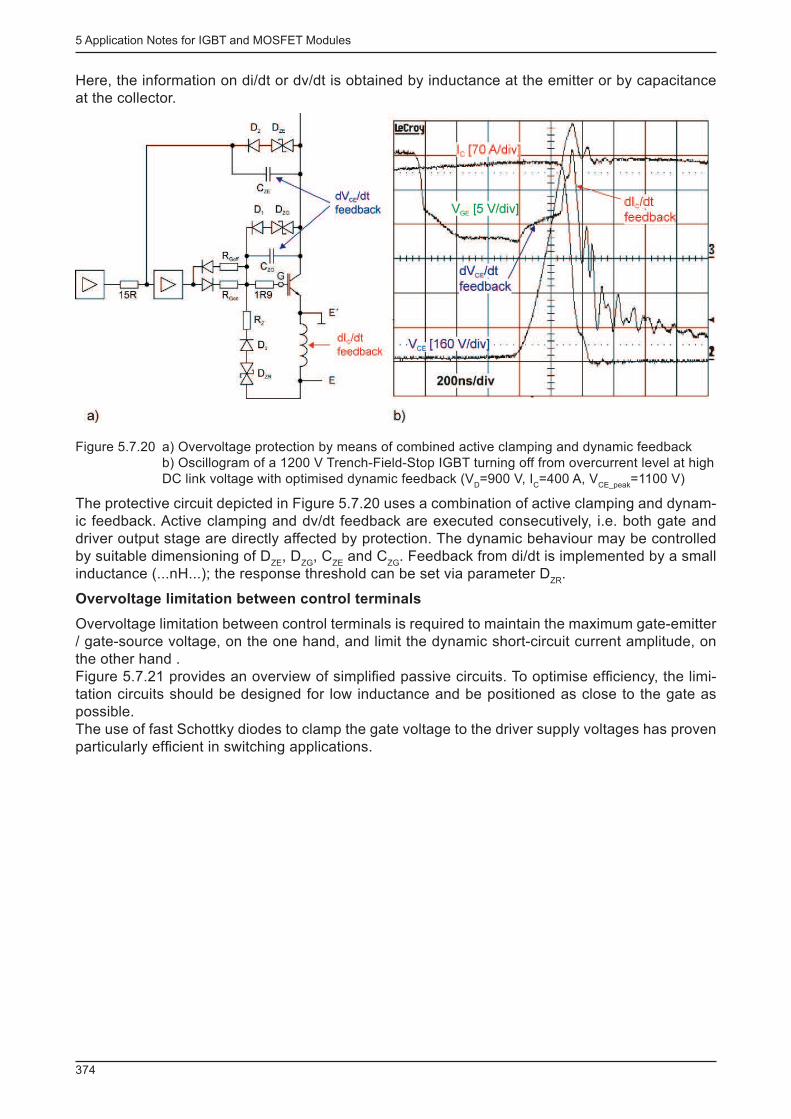
5 Application Notes for IGBT and MOSFET Modules
374
Here, the information on di/dt or dv/dt is obtained by inductance at the emitter or by capacitance at the collector.
Figure 5.7.20 a) Overvoltage protection by means of combined active clamping and dynamic feedbackb) Oscillogram of a 1200 V Trench-Field-Stop IGBT turning off from overcurrent level at high DC link voltage with optimised dynamic feedback (V
D =900 V, I
C =400 A, V
CE_peak =1100 V)
The protective circuit depicted in Figure 5.7.20 uses a combination of active clamping and dynam-ic feedback. Active clamping and dv/dt feedback are executed consecutively, i.e. both gate and driver output stage are directly affected by protection. The dynamic behaviour may be controlled by suitable dimensioning of D
ZE , D
ZG , C
ZE and C
ZG . Feedback from di/dt is implemented by a small
inductance (...nH...); the response threshold can be set via parameter D ZR
.
Overvoltage limitation between control terminals
Overvoltage limitation between control terminals is required to maintain the maximum gate-emitter / gate-source voltage, on the one hand, and limit the dynamic short-circuit current amplitude, on the other hand .Figure 5.7.21 provides an overview of simplifi ed passive circuits. To optimise effi ciency, the limi-tation circuits should be designed for low inductance and be positioned as close to the gate as possible.The use of fast Schottky diodes to clamp the gate voltage to the driver supply voltages has proven particularly effi cient in switching applications.
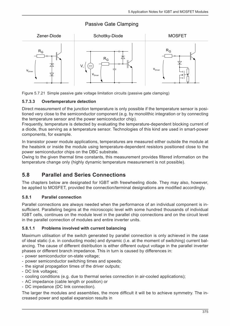
5 Application Notes for IGBT and MOSFET Modules
375
vDriver
RGRG
vDriver
RG
vDriver
V+
Passive Gate Clamping
Zener-Diode Schottky-Diode MOSFET
Figure 5.7.21 Simple passive gate voltage limitation circuits (passive gate clamping)
5.7.3.3 Overtemperature detection
Direct measurement of the junction temperature is only possible if the temperature sensor is posi-tioned very close to the semiconductor component (e.g. by monolithic integration or by connecting the temperature sensor and the power semiconductor chip).Frequently, temperature is detected by evaluating the temperature-dependent blocking current of a diode, thus serving as a temperature sensor. Technologies of this kind are used in smart-power components, for example.
In transistor power module applications, temperatures are measured either outside the module at the heatsink or inside the module using temperature-dependent resistors positioned close to the power semiconductor chips on the DBC substrate. Owing to the given thermal time constants, this measurement provides fi ltered information on the temperature change only (highly dynamic temperature measurement is not possible).
5.8 Parallel and Series Connections
The chapters below are designated for IGBT with freewheeling diode. They may also, however, be applied to MOSFET, provided the connection/terminal designations are modifi ed accordingly.
5.8.1 Parallel connection
Parallel connections are always needed when the performance of an individual component is in-suffi cient. Paralleling begins at the microscopic level with some hundred thousands of individual IGBT cells, continues on the module level in the parallel chip connections and on the circuit level in the parallel connection of modules and entire inverter units.
5.8.1.1 Problems involved with current balancing
Maximum utilisation of the switch generated by parallel connection is only achieved in the case of ideal static (i.e. in conducting mode) and dynamic (i.e. at the moment of switching) current bal-ancing. The cause of different distribution is either different output voltage in the parallel inverter phases or different branch impedance. This in turn is caused by differences in: - power semiconductor on-state voltage; - power semiconductor switching times and speeds; - the signal propagation times of the driver outputs; - DC link voltages; - cooling conditions (e.g. due to thermal series connection in air-cooled applications); - AC impedance (cable length or position) or - DC impedance (DC link connection).
The larger the modules and assemblies, the more diffi cult it will be to achieve symmetry. The in-creased power and spatial expansion results in
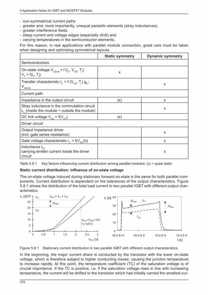
5 Application Notes for IGBT and MOSFET Modules
376
- non-symmetrical current paths - greater and, more importantly, unequal parasitic elements (stray inductances) - greater interference fi elds - steep current and voltage edges (especially di/dt) and - varying temperatures in the semiconductor elements.
For this reason, in real applications with parallel module connection, great care must be taken when designing and optimising symmetrical layouts.
Static symmetry Dynamic symmetry
Semiconductors
On-state voltage V CEsat
= f (i C , V
GE , T
j );
V F = f(i
F , T
j );
x
Transfer characteristic I C = f (V
GE , T
j ) g
fs ;
V GE(th)
x
Current path
Impedance in the output circuit (x) x
Stray inductance in the commutation circuit L
s (inside the module + outside the module)
x
DC link voltage V out
= f(V CC
) (x)
Driver circuit
Output impedance driver(incl. gate series resistance)
x
Gate voltage characteristic i C = f(V
GE (t)) x
Inductance L E
carrying emitter current inside the driver circuit
x
Table 5.8.1 Key factors infl uencing current distribution among parallel modules; (x) = quasi static
Static current distribution: infl uence of on-state voltage
The on-state voltage induced during stationary forward on-state is the same for both parallel com-ponents. Current distribution is dependent on the tolerances of the output characteristics. Figure 5.8.1 shows the distribution of the total load current to two parallel IGBT with different output char-acteristics.
0
5
10
15
20
25
30
0
10
20
30
40
00.0 E+0
t [s]
IC [A]
DIdyn.
DIstat. IC1
IC2
VCE [V]
IC [A] IC1
IC2
Iload = IC1 + IC2
VGE1=VGE2=15V
TJ=125°C
DIstat
05.0 E-6 10.0 E-6 15.0 E-60 0.5 1 1.5 2 2.5 3
Figure 5.8.1 Stationary current distribution in two parallel IGBT with different output characteristics.
In the beginning, the major current share is conducted by the transistor with the lower on-state voltage, which is therefore subject to higher conducting losses, causing the junction temperature to increase rapidly. At this point, the temperature coeffi cient (TC) of the saturation voltage is of crucial importance. If the TC is positive, i.e. if the saturation voltage rises in line with increasing temperature, the current will be shifted to the transistor which had initially carried the smallest cur-
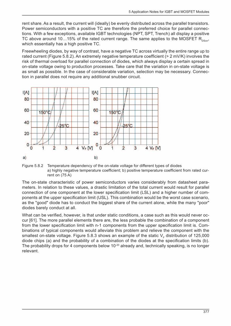
5 Application Notes for IGBT and MOSFET Modules
377
rent share. As a result, the current will (ideally) be evenly distributed across the parallel transistors. Power semiconductors with a positive TC are therefore the preferred choice for parallel connec-tions. With a few exceptions, available IGBT technologies (NPT, SPT, Trench) all display a positive TC above around 10…15% of the rated current range. The same applies to the MOSFET R
DSon ,
which essentially has a high positive TC.
Freewheeling diodes, by way of contrast, have a negative TC across virtually the entire range up to rated current (Figure 5.8.2). An extremely negative temperature coeffi cient (> 2 mV/K) involves the risk of thermal overload for parallel connection of diodes, which always display a certain spread in on-state voltage owing to production processes. Take care that the variation in on-state voltage is as small as possible. In the case of considerable variation, selection may be necessary. Connec-tion in parallel does not require any additional snubber circuit.
Figure 5.8.2 Temperature dependency of the on-state voltage for different types of diodesa) highly negative temperature coeffi cient; b) positive temperature coeffi cient from rated cur-rent on (75 A)
The on-state characteristic of power semiconductors varies considerably from datasheet para-meters. In relation to these values, a drastic limitation of the total current would result for parallel connection of one component at the lower specifi cation limit (LSL) and a higher number of com-ponents at the upper specifi cation limit (USL). This combination would be the worst case scenario, as the "good" diode has to conduct the biggest share of the current alone, while the many "poor" diodes barely conduct at all.
What can be verifi ed, however, is that under static conditions, a case such as this would never oc-cur [61]. The more parallel elements there are, the less probable the combination of a component from the lower specifi cation limit with n-1 components from the upper specifi cation limit is. Com-binations of typical components would alleviate this problem and relieve the component with the smallest on-state voltage. Figure 5.8.3 shows an example of the static V
F distribution of 125,000
diode chips (a) and the probability of a combination of the diodes at the specifi cation limits (b). The probability drops for 4 components below 10-20 already and, technically speaking, is no longer relevant.
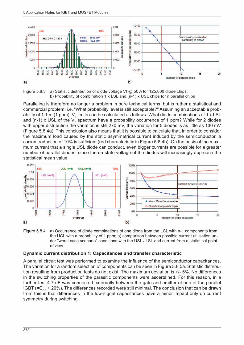
5 Application Notes for IGBT and MOSFET Modules
378
Figure 5.8.3 a) Statistic distribution of diode voltage Vf @ 50 A for 125,000 diode chips; b) Probability of combination 1 x LSL and (n-1) x USL chips for n parallel chips
Paralleling is therefore no longer a problem in pure technical terms, but is rather a statistical and commercial problem, i.e. "What probability level is still acceptable?" Assuming an acceptable prob-ability of 1:1 m (1 ppm), V
F limits can be calculated as follows: What diode combinations of 1 x LSL
and (n-1) x USL of the V F spectrum have a probability occurrence of 1 ppm? While for 2 diodes
with upper distribution the variation is still 270 mV, the variation for 5 diodes is as little as 130 mV (Figure 5.8.4a). This conclusion also means that it is possible to calculate that, in order to consider the maximum load caused by the static asymmetrical current induced by the semiconductor, a current reduction of 10% is suffi cient (red characteristic in Figure 5.8.4b). On the basis of the maxi-mum current that a single USL diode can conduct, even bigger currents are possible for a greater number of parallel diodes, since the on-state voltage of the diodes will increasingly approach the statistical mean value.
Figure 5.8.4 a) Occurrence of diode combinations of one diode from the LCL with n-1 components from the UCL with a probability of 1 ppm; b) comparison between possible current utilisation un-der "worst case scenario" conditions with the USL / LSL and current from a statistical point of view
Dynamic current distribution 1: Capacitances and transfer characteristic
A parallel circuit test was performed to examine the infl uence of the semiconductor capacitances. The variation for a random selection of components can be seen in Figure 5.8.5a. Statistic distribu-tion resulting from production tests do not exist. The maximum deviation is +/- 5%. No differences in the switching properties of the parasitic components were ascertained. For this reason, in a further test 4.7 nF was connected externally between the gate and emitter of one of the parallel IGBT (=C
GE + 20%). The differences recorded were still minimal. The conclusion that can be drawn
from this is that differences in the low-signal capacitances have a minor impact only on current symmetry during switching.
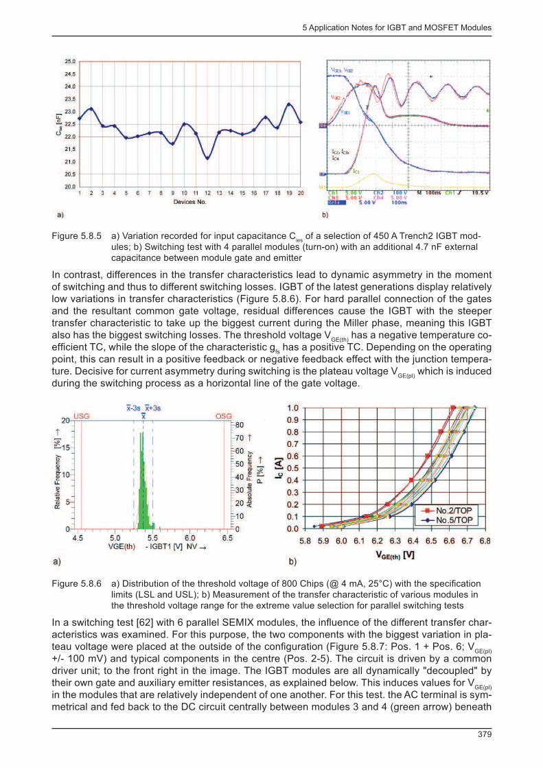
5 Application Notes for IGBT and MOSFET Modules
379
Figure 5.8.5 a) Variation recorded for input capacitance C ies
of a selection of 450 A Trench2 IGBT mod-ules; b) Switching test with 4 parallel modules (turn-on) with an additional 4.7 nF external capacitance between module gate and emitter
In contrast, differences in the transfer characteristics lead to dynamic asymmetry in the moment of switching and thus to different switching losses. IGBT of the latest generations display relatively low variations in transfer characteristics (Figure 5.8.6). For hard parallel connection of the gates and the resultant common gate voltage, residual differences cause the IGBT with the steeper transfer characteristic to take up the biggest current during the Miller phase, meaning this IGBT also has the biggest switching losses. The threshold voltage V
GE(th) has a negative temperature co-
effi cient TC, while the slope of the characteristic g fs has a positive TC. Depending on the operating
point, this can result in a positive feedback or negative feedback effect with the junction tempera-ture. Decisive for current asymmetry during switching is the plateau voltage V
GE(pl) which is induced
during the switching process as a horizontal line of the gate voltage.
Figure 5.8.6 a) Distribution of the threshold voltage of 800 Chips (@ 4 mA, 25°C) with the specifi cation limits (LSL and USL); b) Measurement of the transfer characteristic of various modules in the threshold voltage range for the extreme value selection for parallel switching tests
In a switching test [62] with 6 parallel SEMIX modules, the infl uence of the different transfer char-acteristics was examined. For this purpose, the two components with the biggest variation in pla-teau voltage were placed at the outside of the confi guration (Figure 5.8.7: Pos. 1 + Pos. 6; V
GE(pl)
+/- 100 mV) and typical components in the centre (Pos. 2-5). The circuit is driven by a common driver unit; to the front right in the image. The IGBT modules are all dynamically "decoupled" by their own gate and auxiliary emitter resistances, as explained below. This induces values for V
GE(pl)
in the modules that are relatively independent of one another. For this test. the AC terminal is sym-metrical and fed back to the DC circuit centrally between modules 3 and 4 (green arrow) beneath
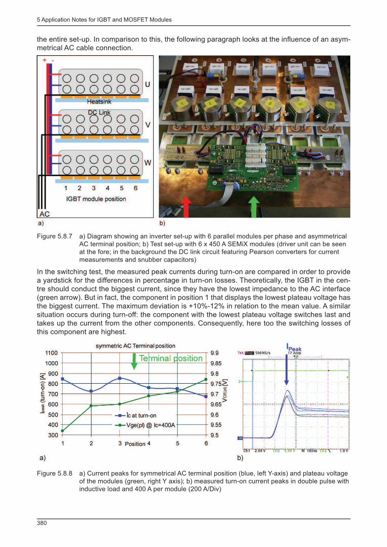
5 Application Notes for IGBT and MOSFET Modules
380
the entire set-up. In comparison to this, the following paragraph looks at the infl uence of an asym-metrical AC cable connection.
Figure 5.8.7 a) Diagram showing an inverter set-up with 6 parallel modules per phase and asymmetrical AC terminal position; b) Test set-up with 6 x 450 A SEMiX modules (driver unit can be seen at the fore; in the background the DC link circuit featuring Pearson converters for current measurements and snubber capacitors)
In the switching test, the measured peak currents during turn-on are compared in order to provide a yardstick for the differences in percentage in turn-on losses. Theoretically, the IGBT in the cen-tre should conduct the biggest current, since they have the lowest impedance to the AC interface (green arrow). But in fact, the component in position 1 that displays the lowest plateau voltage has the biggest current. The maximum deviation is +10%-12% in relation to the mean value. A similar situation occurs during turn-off: the component with the lowest plateau voltage switches last and takes up the current from the other components. Consequently, here too the switching losses of this component are highest.
Figure 5.8.8 a) Current peaks for symmetrical AC terminal position (blue, left Y-axis) and plateau voltage of the modules (green, right Y axis); b) measured turn-on current peaks in double pulse with inductive load and 400 A per module (200 A/Div)
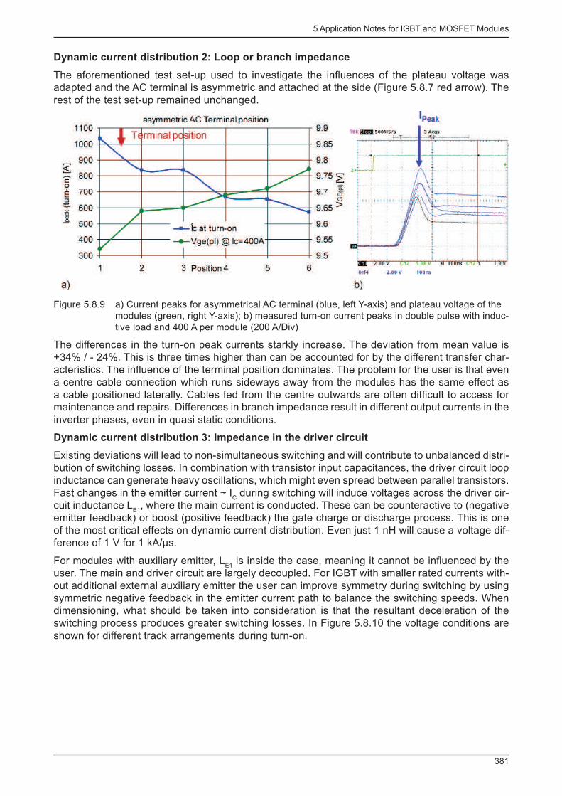
5 Application Notes for IGBT and MOSFET Modules
381
Dynamic current distribution 2: Loop or branch impedance
The aforementioned test set-up used to investigate the infl uences of the plateau voltage was adapted and the AC terminal is asymmetric and attached at the side (Figure 5.8.7 red arrow). The rest of the test set-up remained unchanged.
Figure 5.8.9 a) Current peaks for asymmetrical AC terminal (blue, left Y-axis) and plateau voltage of the modules (green, right Y-axis); b) measured turn-on current peaks in double pulse with induc-tive load and 400 A per module (200 A/Div)
The differences in the turn-on peak currents starkly increase. The deviation from mean value is +34% / - 24%. This is three times higher than can be accounted for by the different transfer char-acteristics. The infl uence of the terminal position dominates. The problem for the user is that even a centre cable connection which runs sideways away from the modules has the same effect as a cable positioned laterally. Cables fed from the centre outwards are often diffi cult to access for maintenance and repairs. Differences in branch impedance result in different output currents in the inverter phases, even in quasi static conditions.
Dynamic current distribution 3: Impedance in the driver circuit
Existing deviations will lead to non-simultaneous switching and will contribute to unbalanced distri-bution of switching losses. In combination with transistor input capacitances, the driver circuit loop inductance can generate heavy oscillations, which might even spread between parallel transistors. Fast changes in the emitter current ~ I
C during switching will induce voltages across the driver cir-
cuit inductance L E1
, where the main current is conducted. These can be counteractive to (negative emitter feedback) or boost (positive feedback) the gate charge or discharge process. This is one of the most critical effects on dynamic current distribution. Even just 1 nH will cause a voltage dif-ference of 1 V for 1 kA/µs.
For modules with auxiliary emitter, L E1
is inside the case, meaning it cannot be infl uenced by the user. The main and driver circuit are largely decoupled. For IGBT with smaller rated currents with-out additional external auxiliary emitter the user can improve symmetry during switching by using symmetric negative feedback in the emitter current path to balance the switching speeds. When dimensioning, what should be taken into consideration is that the resultant deceleration of the switching process produces greater switching losses. In Figure 5.8.10 the voltage conditions are shown for different track arrangements during turn-on.
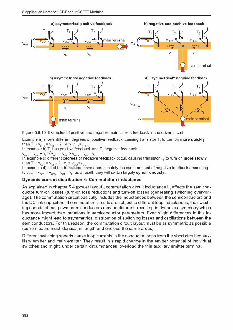
5 Application Notes for IGBT and MOSFET Modules
382
vL
main terminal
vL
vGE
vGE2 vGE3vGE1
c) asymmetrical negative feedback
T1 T2 T3
main terminal
vL
vGE
vGE2 vGE3vGE1
vL
vL
d) „symmetrical“ negative feedback
T1 T2 T3
vL
main terminal
vL
vGE
vGE2 vGE3vGE1
a) asymmetrical positive feedback
vGE
T1 T2 T3
vL
main terminal
vL
vGE
vGE2 vGE3vGE1
b) negative and positive feedback
T1 T2 T3
Figure 5.8.10 Examples of positive and negative main current feedback in the driver circuit
Example a) shows different degrees of positive feedback, causing transistor T 3 to turn on more quickly
than T 1 · v
GE3 = v
GE + 2 · v
L > v
GE1 =v
GE .
In example b) T 2 has positive feedback and T
3 negative feedback
v GE2
= v GE
+ v L > v
GE1 = v
GE > v
GE3 = v
GE - v
L .
In example c) different degrees of negative feedback occur, causing transistor T 3 to turn on more slowly
than T 1 · v
GE3 = v
GE - 2 · v
L < v
GE1 =v
GE .
In example d) all of the transistors have approximately the same amount of negative feedback amounting to v
GE1 = v
GE2 = v
GE3 = v
GE - v
L ; as a result, they will switch largely synchronously .
Dynamic current distribution 4: Commutation inductance
As explained in chapter 5.4 (power layout), commutation circuit inductance L s affects the semicon-
ductor turn-on losses (turn-on loss reduction) and turn-off losses (generating switching overvolt-age). The commutation circuit basically includes the inductances between the semiconductors and the DC link capacitors. If commutation circuits are subject to different loop inductances, the switch-ing speeds of fast power semiconductors may be different, resulting in dynamic asymmetry which has more impact than variations in semiconductor parameters. Even slight differences in this in-ductance might lead to asymmetrical distribution of switching losses and oscillations between the semiconductors. For this reason, the commutation circuit layout must be as symmetric as possible (current paths must identical in length and enclose the same areas).
Different switching speeds cause loop currents in the conductor loops from the short circuited aux-iliary emitter and main emitter. They result in a rapid change in the emitter potential of individual switches and might, under certain circumstances, overload the thin auxiliary emitter terminal.
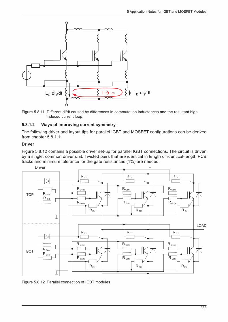
5 Application Notes for IGBT and MOSFET Modules
383
LE di2/dtLE di1/dt I à ¥. .
Figure 5.8.11 Different di/dt caused by differences in commutation inductances and the resultant high induced current loop
5.8.1.2 Ways of improving current symmetry
The following driver and layout tips for parallel IGBT and MOSFET confi gurations can be derived from chapter 5.8.1.1:
Driver
Figure 5.8.12 contains a possible driver set-up for parallel IGBT connections. The circuit is driven by a single, common driver unit. Twisted pairs that are identical in length or identical-length PCB tracks and minimum tolerance for the gate resistances (1%) are needed.
Driver
LOAD
TOP
BOT
+
_
R Goffx
R Goff
R Gon
R Gonx R Gonx R Gonx
R Goffx R Goffx
R CX R CX R CX
R EX R EX R EX
R Gon
R Gon
R EX
R Goffx
R Gonx R Gonx R Gonx
R Goffx R Goffx
R EX R EX
R CX R CX R CX
Figure 5.8.12 Parallel connection of IGBT modules
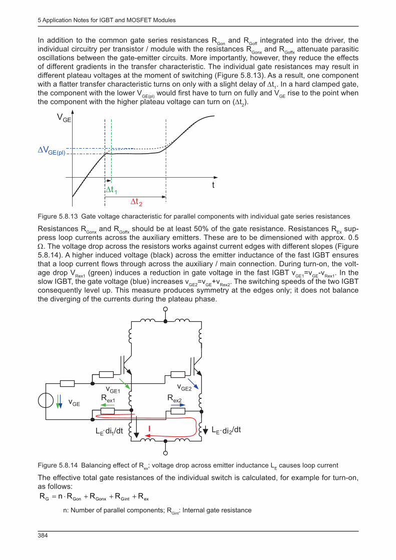
5 Application Notes for IGBT and MOSFET Modules
384
In addition to the common gate series resistances R Gon
and R Goff
integrated into the driver, the individual circuitry per transistor / module with the resistances R
Gonx and R
Goffx attenuate parasitic
oscillations between the gate-emitter circuits. More importantly, however, they reduce the effects of different gradients in the transfer characteristic. The individual gate resistances may result in different plateau voltages at the moment of switching (Figure 5.8.13). As a result, one component with a fl atter transfer characteristic turns on only with a slight delay of ∆t
1 . In a hard clamped gate,
the component with the lower V GE(pl)
would fi rst have to turn on fully and V GE
rise to the point when the component with the higher plateau voltage can turn on (∆t
2 ).
VGE
t
Dt2
Dt1
DVGE(pl)
Figure 5.8.13 Gate voltage characteristic for parallel components with individual gate series resistances
Resistances R Gonx
and R Goffx
should be at least 50% of the gate resistance. Resistances R Ex
sup-press loop currents across the auxiliary emitters. These are to be dimensioned with approx. 0.5 Ω. The voltage drop across the resistors works against current edges with different slopes (Figure 5.8.14). A higher induced voltage (black) across the emitter inductance of the fast IGBT ensures that a loop current fl ows through across the auxiliary / main connection. During turn-on, the volt-age drop V
Rex1 (green) induces a reduction in gate voltage in the fast IGBT v
GE1 =v
GE -v
Rex1 . In the
slow IGBT, the gate voltage (blue) increases v GE2
=v GE
+v Rex2
. The switching speeds of the two IGBT consequently level up. This measure produces symmetry at the edges only; it does not balance the diverging of the currents during the plateau phase.
LE di1/dt LE 2/dt
Rex1 Rex2
vGE2vGE1
I
vGE
. di.
Figure 5.8.14 Balancing effect of R ex
; voltage drop across emitter inductance L E causes loop current
The effective total gate resistances of the individual switch is calculated, for example for turn-on, as follows:
exintGGonxGonG RRRRnR +++×=
n: Number of parallel components; R Gint
: Internal gate resistance
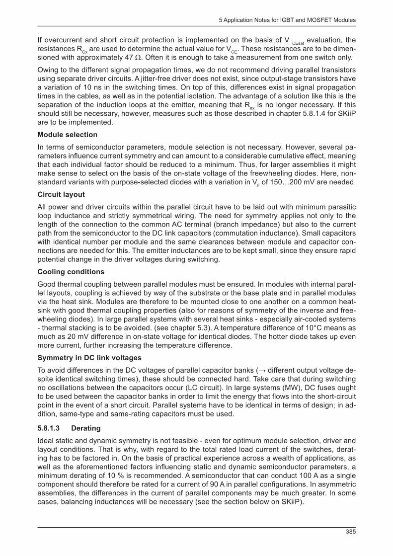
5 Application Notes for IGBT and MOSFET Modules
385
If overcurrent and short circuit protection is implemented on the basis of V CEsat
evaluation, the resistances R
Cx are used to determine the actual value for V
CE . These resistances are to be dimen-
sioned with approximately 47 Ω. Often it is enough to take a measurement from one switch only.
Owing to the different signal propagation times, we do not recommend driving parallel transistors using separate driver circuits. A jitter-free driver does not exist, since output-stage transistors have a variation of 10 ns in the switching times. On top of this, differences exist in signal propagation times in the cables, as well as in the potential isolation. The advantage of a solution like this is the separation of the induction loops at the emitter, meaning that R
ex is no longer necessary. If this
should still be necessary, however, measures such as those described in chapter 5.8.1.4 for SKiiP are to be implemented.
Module selection
In terms of semiconductor parameters, module selection is not necessary. However, several pa-rameters infl uence current symmetry and can amount to a considerable cumulative effect, meaning that each individual factor should be reduced to a minimum. Thus, for larger assemblies it might make sense to select on the basis of the on-state voltage of the freewheeling diodes. Here, non-standard variants with purpose-selected diodes with a variation in V
F of 150…200 mV are needed.
Circuit layout
All power and driver circuits within the parallel circuit have to be laid out with minimum parasitic loop inductance and strictly symmetrical wiring. The need for symmetry applies not only to the length of the connection to the common AC terminal (branch impedance) but also to the current path from the semiconductor to the DC link capacitors (commutation inductance). Small capacitors with identical number per module and the same clearances between module and capacitor con-nections are needed for this. The emitter inductances are to be kept small, since they ensure rapid potential change in the driver voltages during switching.
Cooling conditions
Good thermal coupling between parallel modules must be ensured. In modules with internal paral-lel layouts, coupling is achieved by way of the substrate or the base plate and in parallel modules via the heat sink. Modules are therefore to be mounted close to one another on a common heat-sink with good thermal coupling properties (also for reasons of symmetry of the inverse and free-wheeling diodes). In large parallel systems with several heat sinks - especially air-cooled systems - thermal stacking is to be avoided. (see chapter 5.3). A temperature difference of 10°C means as much as 20 mV difference in on-state voltage for identical diodes. The hotter diode takes up even more current, further increasing the temperature difference.
Symmetry in DC link voltages
To avoid differences in the DC voltages of parallel capacitor banks (→ different output voltage de-spite identical switching times), these should be connected hard. Take care that during switching no oscillations between the capacitors occur (LC circuit). In large systems (MW), DC fuses ought to be used between the capacitor banks in order to limit the energy that fl ows into the short-circuit point in the event of a short circuit. Parallel systems have to be identical in terms of design; in ad-dition, same-type and same-rating capacitors must be used.
5.8.1.3 Derating
Ideal static and dynamic symmetry is not feasible - even for optimum module selection, driver and layout conditions. That is why, with regard to the total rated load current of the switches, derat-ing has to be factored in. On the basis of practical experience across a wealth of applications, as well as the aforementioned factors infl uencing static and dynamic semiconductor parameters, a minimum derating of 10 % is recommended. A semiconductor that can conduct 100 A as a single component should therefore be rated for a current of 90 A in parallel confi gurations. In asymmetric assemblies, the differences in the current of parallel components may be much greater. In some cases, balancing inductances will be necessary (see the section below on SKiiP).
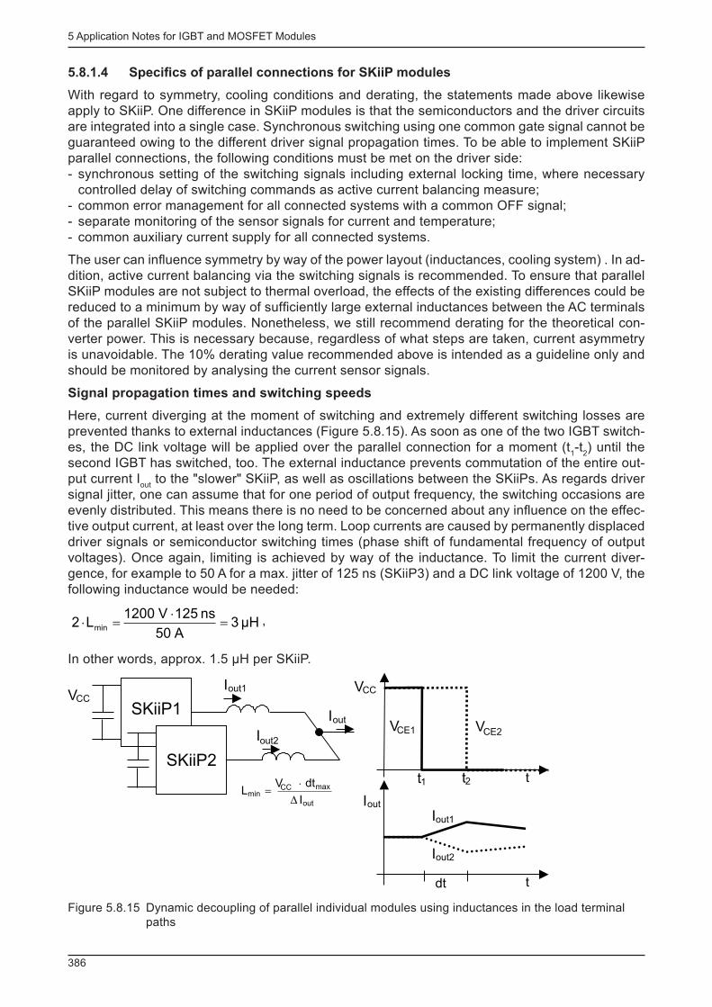
5 Application Notes for IGBT and MOSFET Modules
386
5.8.1.4 Specifi cs of parallel connections for SKiiP modules
With regard to symmetry, cooling conditions and derating, the statements made above likewise apply to SKiiP. One difference in SKiiP modules is that the semiconductors and the driver circuits are integrated into a single case. Synchronous switching using one common gate signal cannot be guaranteed owing to the different driver signal propagation times. To be able to implement SKiiP parallel connections, the following conditions must be met on the driver side: - synchronous setting of the switching signals including external locking time, where necessary controlled delay of switching commands as active current balancing measure;
- common error management for all connected systems with a common OFF signal; - separate monitoring of the sensor signals for current and temperature; - common auxiliary current supply for all connected systems.
The user can infl uence symmetry by way of the power layout (inductances, cooling system) . In ad-dition, active current balancing via the switching signals is recommended. To ensure that parallel SKiiP modules are not subject to thermal overload, the effects of the existing differences could be reduced to a minimum by way of suffi ciently large external inductances between the AC terminals of the parallel SKiiP modules. Nonetheless, we still recommend derating for the theoretical con-verter power. This is necessary because, regardless of what steps are taken, current asymmetry is unavoidable. The 10% derating value recommended above is intended as a guideline only and should be monitored by analysing the current sensor signals.
Signal propagation times and switching speeds
Here, current diverging at the moment of switching and extremely different switching losses are prevented thanks to external inductances (Figure 5.8.15). As soon as one of the two IGBT switch-es, the DC link voltage will be applied over the parallel connection for a moment (t
1 -t
2 ) until the
second IGBT has switched, too. The external inductance prevents commutation of the entire out-put current I
out to the "slower" SKiiP, as well as oscillations between the SKiiPs. As regards driver
signal jitter, one can assume that for one period of output frequency, the switching occasions are evenly distributed. This means there is no need to be concerned about any infl uence on the effec-tive output current, at least over the long term. Loop currents are caused by permanently displaced driver signals or semiconductor switching times (phase shift of fundamental frequency of output voltages). Once again, limiting is achieved by way of the inductance. To limit the current diver-gence, for example to 50 A for a max. jitter of 125 ns (SKiiP3) and a DC link voltage of 1200 V, the following inductance would be needed:
µH3A50
ns125V1200L2 min =
×=× ,
In other words, approx. 1.5 µH per SKiiP.
Iout
Iout1
Iout2
VCC
VCE1
t
VCE2
t
t1 t2
dt
Iout
Iout1
Iout2
VCC
SKiiP1
SKiiP2
out
maxCCmin
I
dtVL
D×
=
Figure 5.8.15 Dynamic decoupling of parallel individual modules using inductances in the load terminal paths
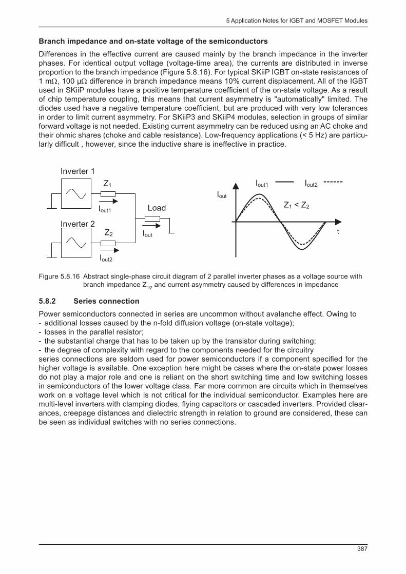
5 Application Notes for IGBT and MOSFET Modules
387
Branch impedance and on-state voltage of the semiconductors
Differences in the effective current are caused mainly by the branch impedance in the inverter phases. For identical output voltage (voltage-time area), the currents are distributed in inverse proportion to the branch impedance (Figure 5.8.16). For typical SKiiP IGBT on-state resistances of 1 mΩ, 100 µΩ difference in branch impedance means 10% current displacement. All of the IGBT used in SKiiP modules have a positive temperature coeffi cient of the on-state voltage. As a result of chip temperature coupling, this means that current asymmetry is "automatically" limited. The diodes used have a negative temperature coeffi cient, but are produced with very low tolerances in order to limit current asymmetry. For SKiiP3 and SKiiP4 modules, selection in groups of similar forward voltage is not needed. Existing current asymmetry can be reduced using an AC choke and their ohmic shares (choke and cable resistance). Low-frequency applications (< 5 Hz) are particu-larly diffi cult , however, since the inductive share is ineffective in practice.
t
Iout
Iout1 Iout2
Z1 < Z2
Z1
Iout1
Inverter 1
Inverter 2Z2
Load
Iout2
Iout
Figure 5.8.16 Abstract single-phase circuit diagram of 2 parallel inverter phases as a voltage source with branch impedance Z
1/2 and current asymmetry caused by differences in impedance
5.8.2 Series connection
Power semiconductors connected in series are uncommon without avalanche effect. Owing to - additional losses caused by the n-fold diffusion voltage (on-state voltage); - losses in the parallel resistor; - the substantial charge that has to be taken up by the transistor during switching; - the degree of complexity with regard to the components needed for the circuitry
series connections are seldom used for power semiconductors if a component specifi ed for the higher voltage is available. One exception here might be cases where the on-state power losses do not play a major role and one is reliant on the short switching time and low switching losses in semiconductors of the lower voltage class. Far more common are circuits which in themselves work on a voltage level which is not critical for the individual semiconductor. Examples here are multi-level inverters with clamping diodes, fl ying capacitors or cascaded inverters. Provided clear-ances, creepage distances and dielectric strength in relation to ground are considered, these can be seen as individual switches with no series connections.

5 Application Notes for IGBT and MOSFET Modules
388
Clamping diodes Flying capacitors Cascaded inverter
Figure 5.8.17 Examples of IGBT series connection without critical voltage distribution
5.8.2.1 The importance of voltage symmetry
To increase the blocking voltage of power electronic switches, IGBT modules may be connected in series. In module applications, series connection applies to both the transistors and the corre-sponding inverse and freewheeling diodes.
Maximum utilisation of the switch generated by series connection is only achieved in the case of ideal static (i.e. in blocking mode) and dynamic (i.e. at the moment of switching) voltage balancing among the individual modules. This is why, in real applications where series connection is used, it is crucial that symmetry be optimised.
Static symmetry Dynamic symmetry
Semiconductors
Blocking current i CES
= f (V CE
, T j ) x
Transfer characteristic I C = f(V
GE , T
j ) g
fs ;
V GE(th)
x
Current path
Total loop inductance(inside module + external)
x
Driver circuit
Output impedance driver(incl. gate series resistances)
x
Gate voltage characteristic V CE
= f (V GE
(t), T
j )
x
Inductance L E
carrying emitter current inside the driver circuit
x
Table 5.8.2 Main factors infl uencing voltage symmetry in series-connected IGBT
Cause of static asymmetry
During stationary off-state, symmetry is determined by the blocking characteristic of the series-connected semiconductors. The bigger the blocking current or the lower the blocking resistance, the lower the voltage taken up by the series-connected semiconductor. The blocking current in-
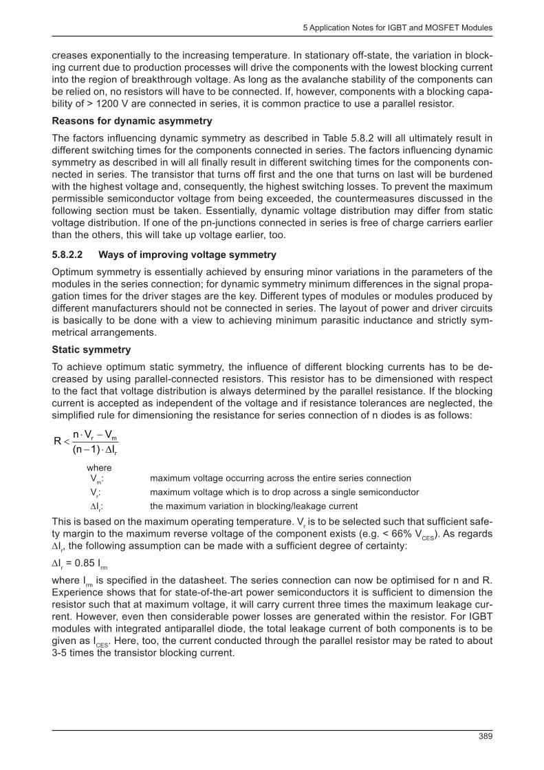
5 Application Notes for IGBT and MOSFET Modules
389
creases exponentially to the increasing temperature. In stationary off-state, the variation in block-ing current due to production processes will drive the components with the lowest blocking current into the region of breakthrough voltage. As long as the avalanche stability of the components can be relied on, no resistors will have to be connected. If, however, components with a blocking capa-bility of > 1200 V are connected in series, it is common practice to use a parallel resistor.
Reasons for dynamic asymmetry
The factors infl uencing dynamic symmetry as described in Table 5.8.2 will all ultimately result in different switching times for the components connected in series. The factors infl uencing dynamic symmetry as described in will all fi nally result in different switching times for the components con-nected in series. The transistor that turns off fi rst and the one that turns on last will be burdened with the highest voltage and, consequently, the highest switching losses. To prevent the maximum permissible semiconductor voltage from being exceeded, the countermeasures discussed in the following section must be taken. Essentially, dynamic voltage distribution may differ from static voltage distribution. If one of the pn-junctions connected in series is free of charge carriers earlier than the others, this will take up voltage earlier, too.
5.8.2.2 Ways of improving voltage symmetry
Optimum symmetry is essentially achieved by ensuring minor variations in the parameters of the modules in the series connection; for dynamic symmetry minimum differences in the signal propa-gation times for the driver stages are the key. Different types of modules or modules produced by different manufacturers should not be connected in series. The layout of power and driver circuits is basically to be done with a view to achieving minimum parasitic inductance and strictly sym-metrical arrangements.
Static symmetry
To achieve optimum static symmetry, the infl uence of different blocking currents has to be de-creased by using parallel-connected resistors. This resistor has to be dimensioned with respect to the fact that voltage distribution is always determined by the parallel resistance. If the blocking current is accepted as independent of the voltage and if resistance tolerances are neglected, the simplifi ed rule for dimensioning the resistance for series connection of n diodes is as follows:
r
mr
I1)(n
VVnR
D×--×
<
where V
m : maximum voltage occurring across the entire series connection
V r : maximum voltage which is to drop across a single semiconductor
∆I r : the maximum variation in blocking/leakage current
This is based on the maximum operating temperature. V r is to be selected such that suffi cient safe-
ty margin to the maximum reverse voltage of the component exists (e.g. < 66% V CES
). As regards ∆I
r , the following assumption can be made with a suffi cient degree of certainty:
∆I r = 0.85 I
rm
where I rm
is specifi ed in the datasheet. The series connection can now be optimised for n and R. Experience shows that for state-of-the-art power semiconductors it is suffi cient to dimension the resistor such that at maximum voltage, it will carry current three times the maximum leakage cur-rent. However, even then considerable power losses are generated within the resistor. For IGBT modules with integrated antiparallel diode, the total leakage current of both components is to be given as I
CES . Here, too, the current conducted through the parallel resistor may be rated to about
3-5 times the transistor blocking current.
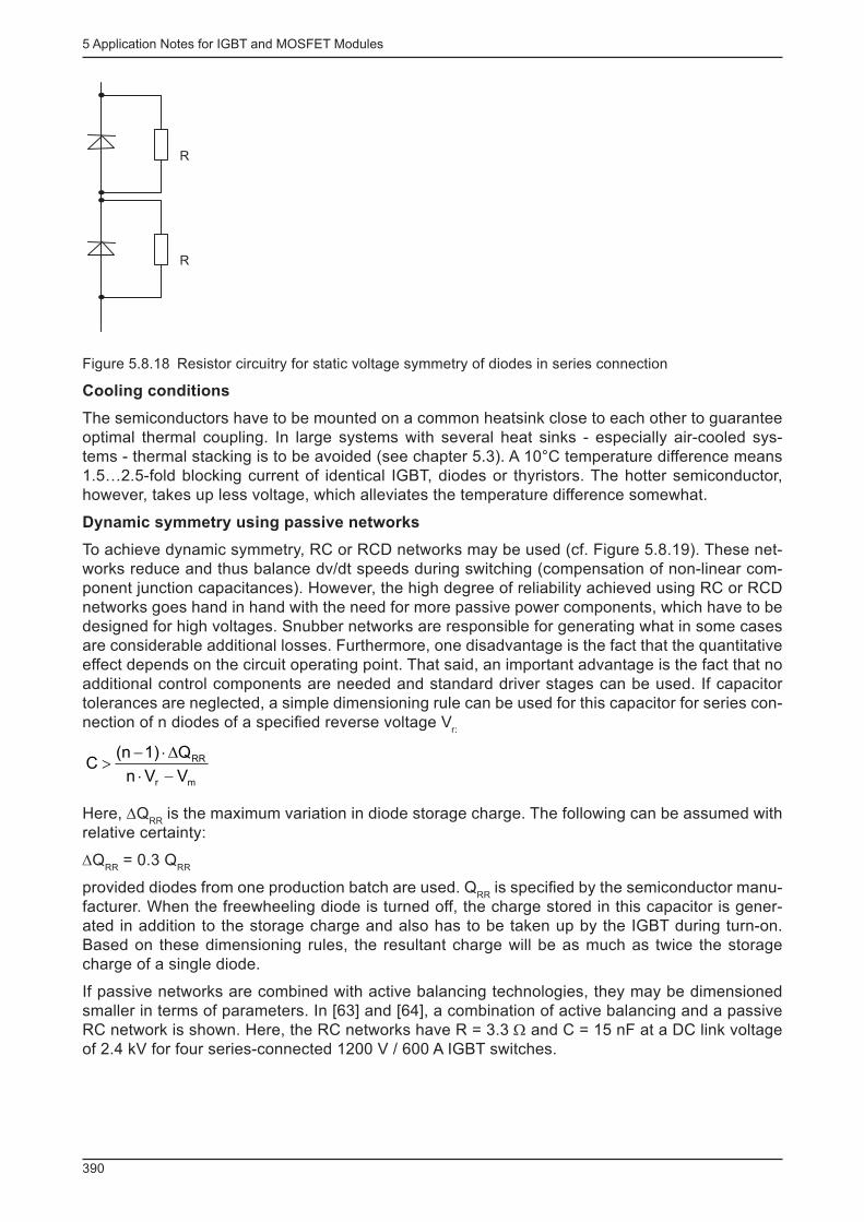
5 Application Notes for IGBT and MOSFET Modules
390
R
R
Figure 5.8.18 Resistor circuitry for static voltage symmetry of diodes in series connection
Cooling conditions
The semiconductors have to be mounted on a common heatsink close to each other to guarantee optimal thermal coupling. In large systems with several heat sinks - especially air-cooled sys-tems - thermal stacking is to be avoided (see chapter 5.3). A 10°C temperature difference means 1.5…2.5-fold blocking current of identical IGBT, diodes or thyristors. The hotter semiconductor, however, takes up less voltage, which alleviates the temperature difference somewhat.
Dynamic symmetry using passive networks
To achieve dynamic symmetry, RC or RCD networks may be used (cf. Figure 5.8.19). These net-works reduce and thus balance dv/dt speeds during switching (compensation of non-linear com-ponent junction capacitances). However, the high degree of reliability achieved using RC or RCD networks goes hand in hand with the need for more passive power components, which have to be designed for high voltages. Snubber networks are responsible for generating what in some cases are considerable additional losses. Furthermore, one disadvantage is the fact that the quantitative effect depends on the circuit operating point. That said, an important advantage is the fact that no additional control components are needed and standard driver stages can be used. If capacitor tolerances are neglected, a simple dimensioning rule can be used for this capacitor for series con-nection of n diodes of a specifi ed reverse voltage V
r :
mr
RR
VVn
Q1)(nC
-×D×-
>
Here, ∆Q RR
is the maximum variation in diode storage charge. The following can be assumed with relative certainty:
∆Q RR
= 0.3 Q RR
provided diodes from one production batch are used. Q RR
is specifi ed by the semiconductor manu-facturer. When the freewheeling diode is turned off, the charge stored in this capacitor is gener-ated in addition to the storage charge and also has to be taken up by the IGBT during turn-on. Based on these dimensioning rules, the resultant charge will be as much as twice the storage charge of a single diode.
If passive networks are combined with active balancing technologies, they may be dimensioned smaller in terms of parameters. In [63] and [64], a combination of active balancing and a passive RC network is shown. Here, the RC networks have R = 3.3 Ω and C = 15 nF at a DC link voltage of 2.4 kV for four series-connected 1200 V / 600 A IGBT switches.
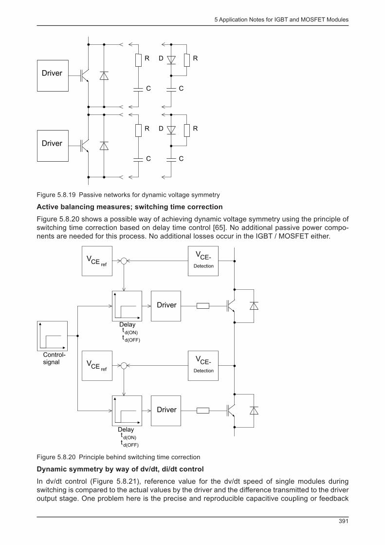
5 Application Notes for IGBT and MOSFET Modules
391
Driver
R
Driver
C
R
C
D
R
C
R
C
D
Figure 5.8.19 Passive networks for dynamic voltage symmetry
Active balancing measures; switching time correction
Figure 5.8.20 shows a possible way of achieving dynamic voltage symmetry using the principle of switching time correction based on delay time control [65]. No additional passive power compo-nents are needed for this process. No additional losses occur in the IGBT / MOSFET either.
VCE ref
Driver
VCE ref
VCE-
Detection
Driver
Delaytd(ON)td(OFF)
Delaytd(ON)td(OFF)
Control-signal
CE-
Detection
V
Figure 5.8.20 Principle behind switching time correction
Dynamic symmetry by way of dv/dt, di/dt control
In dv/dt control (Figure 5.8.21), reference value for the dv/dt speed of single modules during switching is compared to the actual values by the driver and the difference transmitted to the driver output stage. One problem here is the precise and reproducible capacitive coupling or feedback
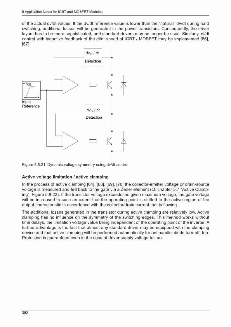
5 Application Notes for IGBT and MOSFET Modules
392
of the actual dv/dt values. If the dv/dt reference value is lower than the "natural" dv/dt during hard switching, additional losses will be generated in the power transistors. Consequently, the driver layout has to be more sophisticated, and standard drivers may no longer be used. Similarly, di/dt control with inductive feedback of the di/dt speed of IGBT / MOSFET may be implemented [66], [67].
dv / dtCE
Detection
InputReference
t
VCE
Detection
dv / dtCE
Figure 5.8.21 Dynamic voltage symmetry using dv/dt control
Active voltage limitation / active clamping
In the process of active clamping [64], [68], [69], [70] the collector-emitter voltage or drain-source voltage is measured and fed back to the gate via a Zener element (cf. chapter 5.7 "Active Clamp-ing", Figure 5.8.22). If the transistor voltage exceeds the given maximum voltage, the gate voltage will be increased to such an extent that the operating point is shifted to the active region of the output characteristic in accordance with the collector/drain current that is fl owing.
The additional losses generated in the transistor during active clamping are relatively low. Active clamping has no infl uence on the symmetry of the switching edges. This method works without time delays, the limitation voltage value being independent of the operating point of the inverter. A further advantage is the fact that almost any standard driver may be equipped with the clamping device and that active clamping will be performed automatically for antiparallel diode turn-off, too. Protection is guaranteed even in the case of driver supply voltage failure.
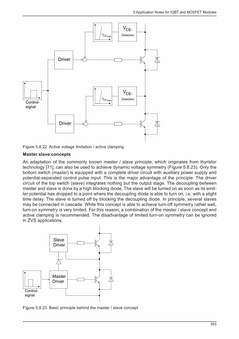
5 Application Notes for IGBT and MOSFET Modules
393
VCE-
Detection
Driver
Control-signal
VCE max
VCE-
Detection
Driver
VCE max
Figure 5.8.22 Active voltage limitation / active clamping
Master slave concepts
An adaptation of the commonly known master / slave principle, which originates from thyristor technology [71], can also be used to achieve dynamic voltage symmetry (Figure 5.8.23). Only the bottom switch (master) is equipped with a complete driver circuit with auxiliary power supply and potential-separated control pulse input. This is the major advantage of the principle. The driver circuit of the top switch (slave) integrates nothing but the output stage. The decoupling between master and slave is done by a high blocking diode. The slave will be turned on as soon as its emit-ter potential has dropped to a point where the decoupling diode is able to turn on, i.e. with a slight time delay. The slave is turned off by blocking the decoupling diode. In principle, several slaves may be connected in cascade. While this concept is able to achieve turn-off symmetry rather well, turn-on symmetry is very limited. For this reason, a combination of the master / slave concept and active clamping is recommended. The disadvantage of limited turn-on symmetry can be ignored in ZVS applications.
SlaveDriver
MasterDriver
Control-signal
Figure 5.8.23 Basic principle behind the master / slave concept

5 Application Notes for IGBT and MOSFET Modules
394
5.8.2.3 Conclusions
In addition to the high-resistance parallel resistors for static symmetry, passive and/or active meas-ures to achieve dynamic symmetry must be taken when IGBT or MOSFET modules are connected in series.
With the exception of active clamping, the methods shown here will protect the transistors only, meaning that additional passive networks will be needed to protect the inverse diodes.
5.9 Soft switching as ZVS or ZCS / switching loss reduction net-
works (snubbers)
5.9.1 Aims and areas of application
Industrial power electronic circuit engineering in the medium and upper power class range is domi-nated by topologies related to impressed direct voltages. In these circuits, IGBT and MOSFET are operated almost exclusively in hard switching mode, i.e. they are subject to high switching losses and power dissipation peaks, resulting in typical switching frequencies between 1 kHz and 30 kHz (IGBT) or 50 - 100 kHz (MOSFET).
Increasing the switching frequency will generally lead to reduction in size and weight of passive energy storage components (chokes, capacitors, transformers, fi lters), which is of interest, for ex-ample, with respect to the integration of transformers into converter systems.
Typical areas of application: - Battery charging, - UPS with potential-isolated DC-DC converter, - electronic power supply units (switch-mode power supply) for general applications, - PFC circuits, - industrial power supply systems (welding, electroplating, inductive heating, x-ray, plasma, etc.).
If the required switching frequencies cannot be obtained in a hard-switch application, either in-terleaved technologies have to be used or the resulting switching losses have to be reduced.Basically, there are two ways of reducing switching losses:
1. Implementation of additional switching loss reduction networks, whilst keeping the basic circuitry (snubber circuit)
2. Soft switching as ZVS ( Z ero V oltage S witch) or ZCS ( Z ero C urrent S witch).
5.9.2 Switching loss reduction networks / snubber circuits
Power-electronic switches with conventional thyristors or GTOs require snubber circuits in order to guarantee operation within the safe operating area, i.e. these networks are indispensable if the components are to live up to their basic functions during switching. In contrast to this, the SOA characteristics of modern IGBT and MOSFET allow operation without the use of networks, mean-ing that additional networks may only serve to reduce switching losses or perform symmetry tasks in the case of cascading.
Figure 5.9.1 shows a conventional buck converter with IGBT and basic networks for turn-on and turn-off relief (reduction of switching losses).
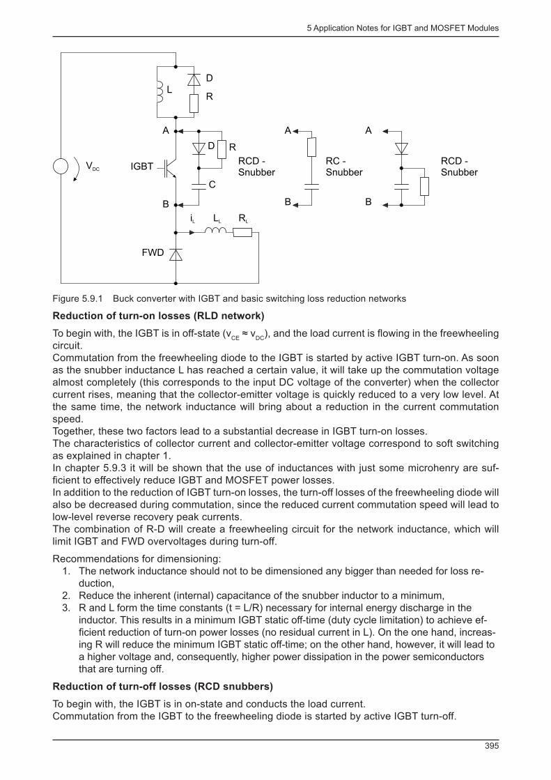
5 Application Notes for IGBT and MOSFET Modules
395
L
VDC
D
R
RD
C
IGBT
A
B
iL RLLL
FWD
RCD -Snubber
A
RC -Snubber
B
A
RCD -Snubber
B
Figure 5.9.1 Buck converter with IGBT and basic switching loss reduction networks
Reduction of turn-on losses (RLD network)
To begin with, the IGBT is in off-state (v CE
≈ v DC
), and the load current is fl owing in the freewheeling circuit.Commutation from the freewheeling diode to the IGBT is started by active IGBT turn-on. As soon as the snubber inductance L has reached a certain value, it will take up the commutation voltage almost completely (this corresponds to the input DC voltage of the converter) when the collector current rises, meaning that the collector-emitter voltage is quickly reduced to a very low level. At the same time, the network inductance will bring about a reduction in the current commutation speed.Together, these two factors lead to a substantial decrease in IGBT turn-on losses.The characteristics of collector current and collector-emitter voltage correspond to soft switching as explained in chapter 1.In chapter 5.9.3 it will be shown that the use of inductances with just some microhenry are suf-fi cient to effectively reduce IGBT and MOSFET power losses.In addition to the reduction of IGBT turn-on losses, the turn-off losses of the freewheeling diode will also be decreased during commutation, since the reduced current commutation speed will lead to low-level reverse recovery peak currents.The combination of R-D will create a freewheeling circuit for the network inductance, which will limit IGBT and FWD overvoltages during turn-off.
Recommendations for dimensioning:1. The network inductance should not to be dimensioned any bigger than needed for loss re-
duction,2. Reduce the inherent (internal) capacitance of the snubber inductor to a minimum,3. R and L form the time constants (t = L/R) necessary for internal energy discharge in the
inductor. This results in a minimum IGBT static off-time (duty cycle limitation) to achieve ef-fi cient reduction of turn-on power losses (no residual current in L). On the one hand, increas-ing R will reduce the minimum IGBT static off-time; on the other hand, however, it will lead to a higher voltage and, consequently, higher power dissipation in the power semiconductors that are turning off.
Reduction of turn-off losses (RCD snubbers)
To begin with, the IGBT is in on-state and conducts the load current.Commutation from the IGBT to the freewheeling diode is started by active IGBT turn-off.

5 Application Notes for IGBT and MOSFET Modules
396
The load current quickly commutates from the IGBT to the parallel D-C branch, causing the collec-tor current and the collector-emitter dv/dt to decrease at the same time.This leads to a reduction in the IGBT turn-off losses. The characteristics for collector current and collector-emitter voltage correspond to soft switching as explained in chapter 1.Chapter 5.9.3 shows that the loss reduction that can be achieved with a certain capacitance strongly depends on the given transistor technology. At the end of voltage commutation, the free-wheeling diode will turn on with low losses and take up the snubber capacitance current. As of the next time the IGBT turns on, the energy stored in the snubber network capacitor will be mainly converted to heat by resistor R.
Recommendations for dimensioning:1. The snubber inductance should not to be dimensioned any bigger than needed for loss re-
duction2. Use fast network diode with lower turn-on overvoltage (forward recovery)3. Use pulse-proof capacitors (fi lm capacitors or similar) with low internal inductance4. Reduce loop inductance in the snubber network to a minimum5. R and C form the time constants (t = R*C) necessary for internal energy discharge in the
capacitor. This results in a minimum IGBT static off-time (duty cycle limitation) to achieve effi -cient reduction of turn-off power losses (no residual voltage in C). On the one hand, decreas-ing R will reduce the minimum IGBT static on-time; on the other hand, however, it will lead to a higher current and, consequently, greater losses when the transistor is turned on.
Note that bigger inductive and capacitive snubber elements will always lead to longer commutation times!
In applications that use simple snubber networks, as described above, the total energy stored is converted to heat mainly in the network resistor but also partially in the transistor (dissipative snub-ber). Thus, the overall effi ciency of the circuit will not be improved - irrespective of the reduced losses in the switches. All this measure does is move the losses from the semiconductor to the snubber resistor, thus allowing higher switching frequencies.Furthermore, numerous low-loss snubber networks (non or low-dissipative snubbers), where the energy is stored in resonant circuits or fed back to the DC link, are well-known from relevant lit-erature. However, circuit designs such as these are often very complicated to dimension, and the layout and circuitry requirements are very challenging, too. [72].
5.9.3 Soft switching
5.9.3.1 Load on power semiconductors
Soft switching is another possible way of reducing losses in power electronic switches.The expression "soft switching" actually refers to the operation of power electronic switches as zero-voltage switches (ZVS) or zero-current switches (ZCS) (cf. chapter 1).The many different converter circuits that working according to these principles are generally as-signed to resonance or quasi-resonance technology.
ZVS (Figure 5.9.3): - The commutation process is started by active turn-off, switching losses are reduced thanks to parallel connection of commutation capacitance C
K ,
- the commutation process is completed by passive, low-loss turn-on at a switch voltage v s ≈ 0,
- before next commutation, the direction of current fl ow changes in the switch that is turned on with impressed di/dt,
- Inductance in commutation circuit L K should be at the minimum.
ZCS (Figure 5.9.5): - The commutation process is started by active turn-on, switching losses are reduced thanks to series connection of commutation inductance L
K ,
- the commutation process is completed by passive, low-loss turn-off at a switch current i s ≈ 0,
- before next commutation, the voltage direction changes in the switch that is turned on with im-
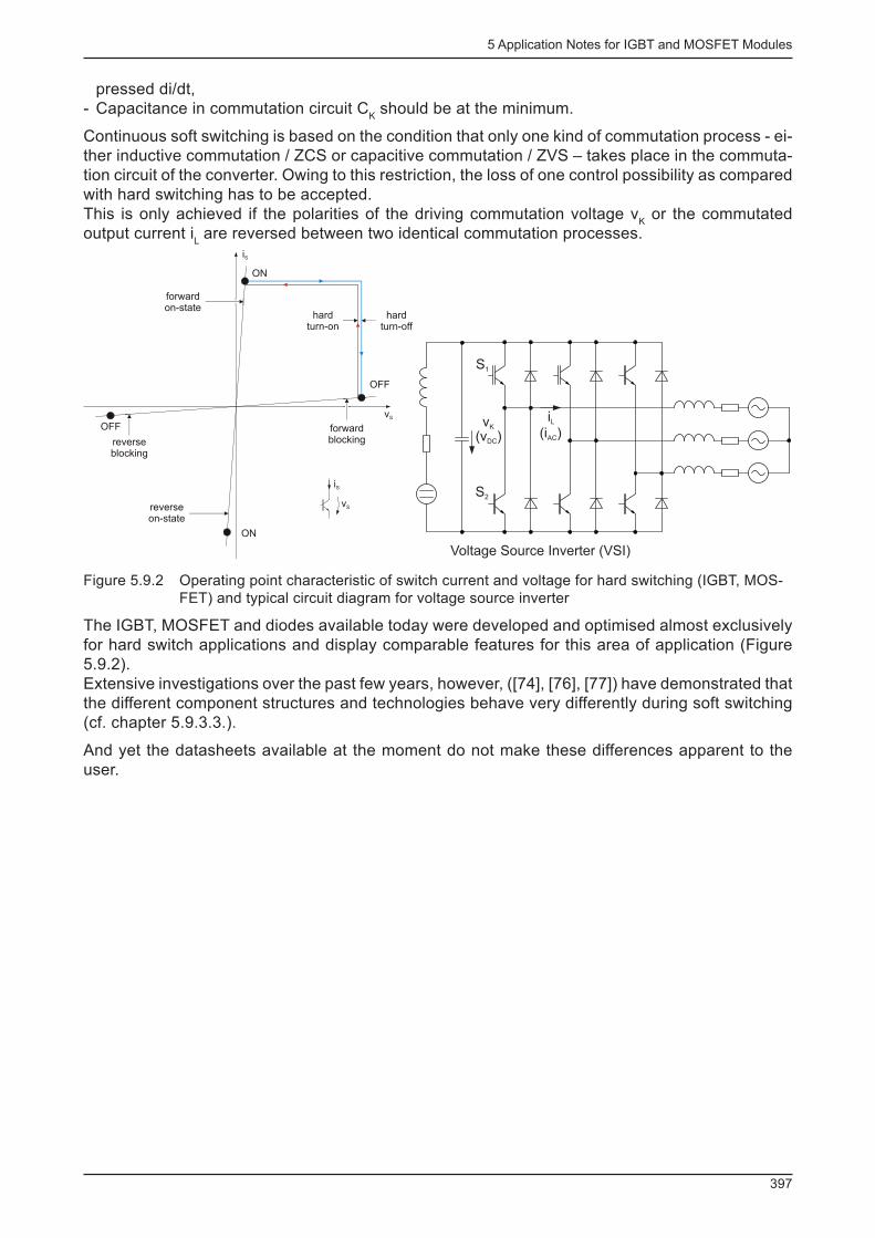
5 Application Notes for IGBT and MOSFET Modules
397
pressed di/dt, - Capacitance in commutation circuit C
K should be at the minimum.
Continuous soft switching is based on the condition that only one kind of commutation process - ei-ther inductive commutation / ZCS or capacitive commutation / ZVS – takes place in the commuta-tion circuit of the converter. Owing to this restriction, the loss of one control possibility as compared with hard switching has to be accepted. This is only achieved if the polarities of the driving commutation voltage v
K or the commutated
output current i L are reversed between two identical commutation processes.
ON
ON
OFF
OFF
reverseon-state
forwardon-state
reverseblocking
forwardblocking
vS
iS
vS
iS
hardturn-off
hardturn-on
S1
S2
iL(i )AC
vK
(v )DC
Voltage Source Inverter (VSI)
Figure 5.9.2 Operating point characteristic of switch current and voltage for hard switching (IGBT, MOS-FET) and typical circuit diagram for voltage source inverter
The IGBT, MOSFET and diodes available today were developed and optimised almost exclusively for hard switch applications and display comparable features for this area of application (Figure 5.9.2).Extensive investigations over the past few years, however, ([74], [76], [77]) have demonstrated that the different component structures and technologies behave very differently during soft switching (cf. chapter 5.9.3.3.).
And yet the datasheets available at the moment do not make these differences apparent to the user.
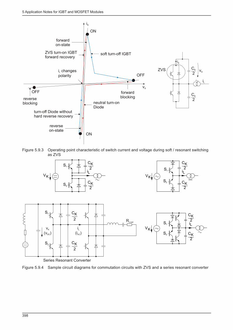
5 Application Notes for IGBT and MOSFET Modules
398
ON
ON
OFF
OFFvS
iS
vS
iS
forwardon-state
soft turn-off IGBT
reverseblocking
forwardblocking
iL
CK
2
reverseon-state
i changespolarityL
turn-off Diode withouthard reverse recovery
ZVS turn-on IGBTforward recovery
neutral turn-onDiode
CK
2
ZVS
Figure 5.9.3 Operating point characteristic of switch current and voltage during soft / resonant switching as ZVS
iLVK
CK2
CK2
S1
S2
CK
2
CK
2
S1
S2
RLoad
v
(v )K
DC
i
(i )L
AC
Series Resonant Converter
CK
2iL
VK
CK
2
S1
S2
VK
iL
CK2
CK2
S2
S1
Figure 5.9.4 Sample circuit diagrams for commutation circuits with ZVS and a series resonant converter
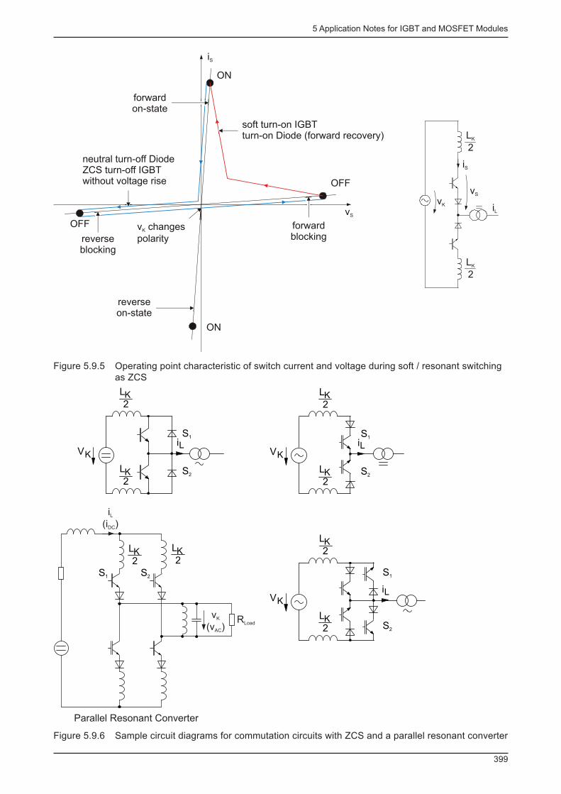
5 Application Notes for IGBT and MOSFET Modules
399
ON
ON
OFF
OFF
reverseon-state
vS
iS
vS
iS
forwardon-state
soft turn-on IGBTturn-on Diode (forward recovery)
neutral turn-off DiodeZCS turn-off IGBTwithout voltage rise
reverseblocking
forwardblocking
v changespolarity
K
vK iL
LK
2
LK
2
Figure 5.9.5 Operating point characteristic of switch current and voltage during soft / resonant switching as ZCS
LK2
LK2
S2S1
RLoad
v
(v )K
AC
i
(i )L
DC
Parallel Resonant Converter
LK
VK
2
iL
LK2
S1
S2
VK
iL
LK2
LK2
S1
S2
VK
iL
LK2
LK2
S1
S2
Figure 5.9.6 Sample circuit diagrams for commutation circuits with ZCS and a parallel resonant converter

5 Application Notes for IGBT and MOSFET Modules
400
A comparison of the track of the operating points in fi gures 5.9.2, 5.9.3 and 5.9.5 shows that the area encircled by the track is different in size. The area is a relative measure of the power losses that occur during switching. During hard switching (Figure 5.9.2) the area is at its maximum. In the case of ideal resonant switching, the track of the operating point would go along the axes of the coordinate system. In real resonant or quasi-resonant switching and commutation processes, the resulting path will lie somewhere between the two aforementioned ideal conditions (Figures 5.9.3 and 5.9.5).
5.9.3.2 Semiconductor and driver requirements
ZVS
Power semiconductors - have to feature active turn-off and demonstrate good power-loss reduction behaviour during turn-off
- For IGBT: + short charge carrier lifetime and low tail charge + low dependence of tail charge and charge carrier lifetime on the junction temperature + low forward turn-on overvoltage during conductivity modulation during zero-voltage
turn-on with impressed di/dt - Since ZVS-diodes do not turn off with reverse-recovery di/dt and take on reverse voltage at the same time, the requirements for reverse-recovery behaviour are not as strict as for hard switch-ing topologies.
Driver circuit:
The driver circuit has to comply with the following minimum requirements: - active IGBT / MOSFET turn-off and - switch voltage monitoring and passive turn-on of ZVS at v
S ≈ 0 V.
Modifi ed ZVS mode:
The duration of a capacitive commutation process can be approximated as follows:
t Kc
≈ (C K · v
K )/i
L
Where: C K : Commutation capacitance (power loss reduction capacitance) v
K : Commutation voltage
i L : Load current to be commutated
With low load currents, the commutation process in power converters may last an undesirably long time, impairing circuit function. This can be avoided by using modifi ed zero voltage switches, which will abruptly end the commutation process after a variable maximum commutation time by active turn-on towards the not yet fully recharged commutation capacitance. This can, however, result in increased switching losses.
Figure 5.9.7 shows the principle behind a modifi ed ZVS.

5 Application Notes for IGBT and MOSFET Modules
401
ON
OFF
1
&
+
-
t
tt
Driver
refv
vS
iS
tKmax
„hard interrupt“ of voltagecommutation in case ofexceeding the max.commutation time
Figure 5.9.7 Modifi ed ZVS: basic principle
ZCS
Power semiconductors - have to feature active turn-on and demonstrate good power-loss reduction behaviour during turn-on,
- should have low internal capacitance, - For IGBT: + short charge carrier lifetime
+ low dependence of storage charge and tail charge on the junction temperature + short dynamic saturation phase during turn-on
- Diodes: Low reverse recovery charge (Q RR
, t RR
)
Driver circuit:
The driver circuit has to comply with the following minimum requirements: - active IGBT / MOSFET turn-on and - switch current monitoring and passive turn-off of ZCS at i
S ≈ 0 A.
Modifi ed ZCS mode: The duration of an inductive commutation process can be approximated as follows:
t Ki ≈ (L
K · i
L )/v
K .
Where: L K : Inductance in the commutation circuit (power loss reduction inductance) vK: Commutation voltage i L : Load current to be commutated
At low commutation voltages or high load currents, the commutation process in power converters may last an undesirably long time, impairing circuit function. This can be avoided by using modifi ed zero current switches, which will abruptly end the commutation process after a variable maximum commutation time by active turn-off towards the live commutation inductance. This can, however, result in increased switching losses. In connection with this, please note that in many applications zero current switches have to feature overvoltage protection.
Figure 5.9.8 shows the principle behind a modifi ed ZCS.
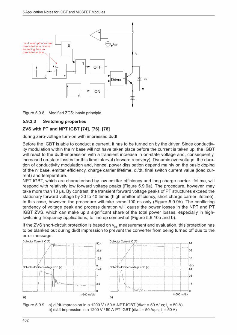
5 Application Notes for IGBT and MOSFET Modules
402
ON
OFF1
&
+
-
t t
t
Driver
refi
vS
iS
tKmax
„hard interrupt“ of currentcommutation in case ofexceeding the max.commutation time
Figure 5.9.8 Modifi ed ZCS: basic principle
5.9.3.3 Switching properties
ZVS with PT and NPT IGBT [74], [76], [78]
during zero-voltage turn-on with impressed di/dt
Before the IGBT is able to conduct a current, it has to be turned on by the driver. Since conductiv-ity modulation within the n - base will not have taken place before the current is taken up, the IGBT will react to the di/dt-impression with a transient increase in on-state voltage and, consequently, increased on-state losses for this time interval (forward recovery). Dynamic overvoltage, the dura-tion of conductivity modulation and, hence, power dissipation depend mainly on the basic doping of the n - base, emitter effi ciency, charge carrier lifetime, di/dt, fi nal switch current value (load cur-rent) and temperature.NPT IGBT, which are characterised by low emitter effi ciency and long charge carrier lifetime, will respond with relatively low forward voltage peaks (Figure 5.9.9a). The procedure, however, may take more than 10 µs. By contrast, the transient forward voltage peaks of PT structures exceed the stationary forward voltage by 30 to 40 times (high emitter effi ciency, short charge carrier lifetime). In this case, however, the procedure will take some 100 ns only (Figure 5.9.9b). The confl icting tendency of voltage peak and process duration will cause the power losses in the NPT and PT IGBT ZVS, which can make up a signifi cant share of the total power losses, especially in high-switching-frequency applications, to line up somewhat (Figure 5.9.10a and b).
If the ZVS short-circuit protection is based on v CE
measurement and evaluation, this protection has to be blanked out during di/dt impression to prevent the converter from being turned off due to the error message.
Collector Current iC [A]
Collector-Emitter-Voltage vCE [V]
50.4
33.6
16.8
0
10.5
7
3.5
0
t=500 ns/div
Collector Current iC [A]
Collector-Emitter-Voltage vCE [V]
54
36
18
-0.3
54
36
18
0
t=500 ns/diva) b)
Figure 5.9.9 a) di/dt-impression in a 1200 V / 50 A-NPT-IGBT (di/dt = 50 A/µs; i L = 50 A)
b) di/dt-impression in a 1200 V / 50 A-PT-IGBT (di/dt = 50 A/µs; i L = 50 A)
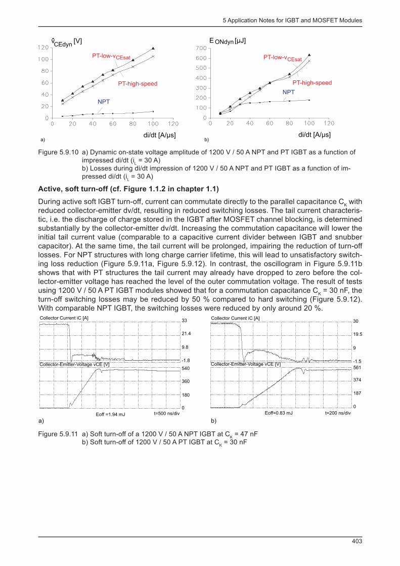
5 Application Notes for IGBT and MOSFET Modules
403
di/dt [A/µs]
PT-high-speed
PT-low-v
NPT
CEsat
v [V]CEdyn
E [µJ]ONdyn
di/dt [A/µs]
NPT
PT-high-speed
PT-low-vCEsat
a) b)
Figure 5.9.10 a) Dynamic on-state voltage amplitude of 1200 V / 50 A NPT and PT IGBT as a function of impressed di/dt (i
L = 30 A)
b) Losses during di/dt impression of 1200 V / 50 A NPT and PT IGBT as a function of im-pressed di/dt (i
L = 30 A)
Active, soft turn-off (cf. Figure 1.1.2 in chapter 1.1)
During active soft IGBT turn-off, current can commutate directly to the parallel capacitance C K with
reduced collector-emitter dv/dt, resulting in reduced switching losses. The tail current characteris-tic, i.e. the discharge of charge stored in the IGBT after MOSFET channel blocking, is determined substantially by the collector-emitter dv/dt. Increasing the commutation capacitance will lower the initial tail current value (comparable to a capacitive current divider between IGBT and snubber capacitor). At the same time, the tail current will be prolonged, impairing the reduction of turn-off losses. For NPT structures with long charge carrier lifetime, this will lead to unsatisfactory switch-ing loss reduction (Figure 5.9.11a, Figure 5.9.12). In contrast, the oscillogram in Figure 5.9.11b shows that with PT structures the tail current may already have dropped to zero before the col-lector-emitter voltage has reached the level of the outer commutation voltage. The result of tests using 1200 V / 50 A PT IGBT modules showed that for a commutation capacitance C
K = 30 nF, the
turn-off switching losses may be reduced by 50 % compared to hard switching (Figure 5.9.12). With comparable NPT IGBT, the switching losses were reduced by only around 20 %.
Collector Current iC [A]
Collector-Emitter-Voltage vCE [V]
33
21.4
9.8
-1.8
540
360
180
0
t=500 ns/divEoff =1.94 mJ
Collector Current iC [A]
Collector-Emitter-Voltage vCE [V]
30
19.5
9
-1.5
561
374
187
0
t=200 ns/divEoff=0.83 mJ
a) b)
Figure 5.9.11 a) Soft turn-off of a 1200 V / 50 A NPT IGBT at C K = 47 nF
b) Soft turn-off of 1200 V / 50 A PT IGBT at C K = 30 nF
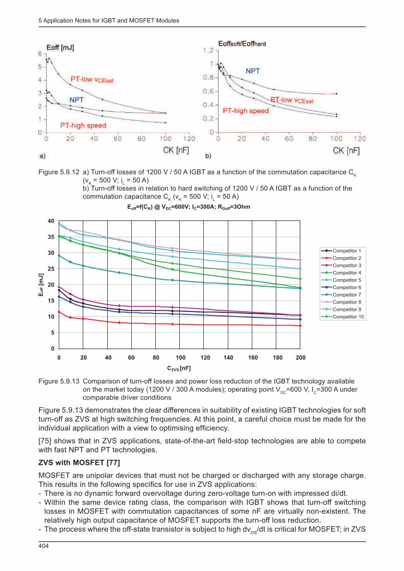
5 Application Notes for IGBT and MOSFET Modules
404
Figure 5.9.12 a) Turn-off losses of 1200 V / 50 A IGBT as a function of the commutation capacitance C K
(v K = 500 V; i
L = 50 A)
b) Turn-off losses in relation to hard switching of 1200 V / 50 A IGBT as a function of the commutation capacitance C
K (v
K = 500 V; i
L = 50 A)
Eoff=f(CK) @ VDC=600V; IC=300A; RGoff=3Ohm
0
5
10
15
20
25
30
35
40
0 20 40 60 80 100 120 140 160 180 200
CZVS
Eo
ff[m
J]
Competitor 1
Competitor 2
Competitor 3
Competitor 4
Competitor 5
Competitor 6
Competitor 7
Competitor 8
Competitor 9
Competitor 10
[nF]
Figure 5.9.13 Comparison of turn-off losses and power loss reduction of the IGBT technology available on the market today (1200 V / 300 A modules); operating point V
DC =600 V, I
C =300 A under
comparable driver conditions
Figure 5.9.13 demonstrates the clear differences in suitability of existing IGBT technologies for soft turn-off as ZVS at high switching frequencies. At this point, a careful choice must be made for the individual application with a view to optimising effi ciency.
[75] shows that in ZVS applications, state-of-the-art fi eld-stop technologies are able to compete with fast NPT and PT technologies.
ZVS with MOSFET [77]
MOSFET are unipolar devices that must not be charged or discharged with any storage charge. This results in the following specifi cs for use in ZVS applications: - There is no dynamic forward overvoltage during zero-voltage turn-on with impressed di/dt. - Within the same device rating class, the comparison with IGBT shows that turn-off switching losses in MOSFET with commutation capacitances of some nF are virtually non-existent. The relatively high output capacitance of MOSFET supports the turn-off loss reduction.
- The process where the off-state transistor is subject to high dv DS
/dt is critical for MOSFET; in ZVS
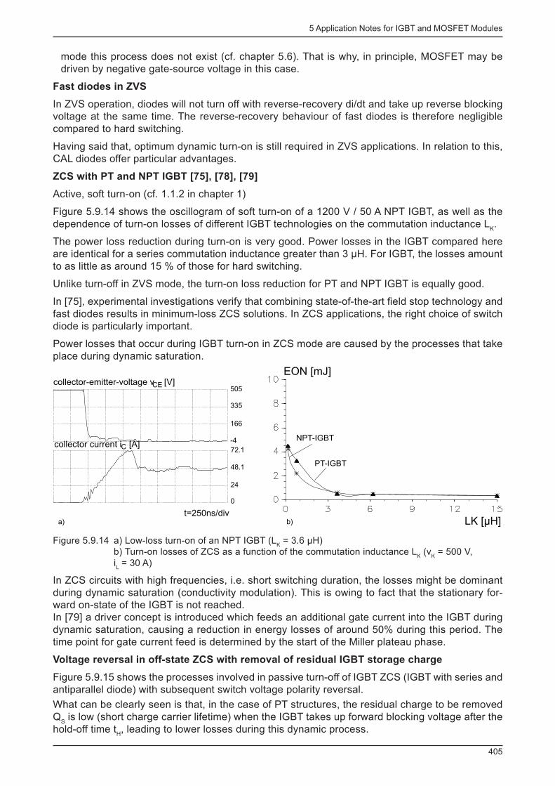
5 Application Notes for IGBT and MOSFET Modules
405
mode this process does not exist (cf. chapter 5.6). That is why, in principle, MOSFET may be driven by negative gate-source voltage in this case.
Fast diodes in ZVS
In ZVS operation, diodes will not turn off with reverse-recovery di/dt and take up reverse blocking voltage at the same time. The reverse-recovery behaviour of fast diodes is therefore negligible compared to hard switching.
Having said that, optimum dynamic turn-on is still required in ZVS applications. In relation to this, CAL diodes offer particular advantages.
ZCS with PT and NPT IGBT [75], [78], [79]
Active, soft turn-on (cf. 1.1.2 in chapter 1)
Figure 5.9.14 shows the oscillogram of soft turn-on of a 1200 V / 50 A NPT IGBT, as well as the dependence of turn-on losses of different IGBT technologies on the commutation inductance L
K .
The power loss reduction during turn-on is very good. Power losses in the IGBT compared here are identical for a series commutation inductance greater than 3 µH. For IGBT, the losses amount to as little as around 15 % of those for hard switching.
Unlike turn-off in ZVS mode, the turn-on loss reduction for PT and NPT IGBT is equally good.
In [75], experimental investigations verify that combining state-of-the-art fi eld stop technology and fast diodes results in minimum-loss ZCS solutions. In ZCS applications, the right choice of switch diode is particularly important.
Power losses that occur during IGBT turn-on in ZCS mode are caused by the processes that take place during dynamic saturation.
collector current i [A]
collector-emitter-voltage v [V]
C
CE505
335
166
-4
72.1
48.1
24
0
t=250ns/div
EON [mJ]
LK [µH]
NPT-IGBT
PT-IGBT
a) b)
Figure 5.9.14 a) Low-loss turn-on of an NPT IGBT (L K = 3.6 µH)
b) Turn-on losses of ZCS as a function of the commutation inductance L K (v
K = 500 V,
i L = 30 A)
In ZCS circuits with high frequencies, i.e. short switching duration, the losses might be dominant during dynamic saturation (conductivity modulation). This is owing to fact that the stationary for-ward on-state of the IGBT is not reached.In [79] a driver concept is introduced which feeds an additional gate current into the IGBT during dynamic saturation, causing a reduction in energy losses of around 50% during this period. The time point for gate current feed is determined by the start of the Miller plateau phase.
Voltage reversal in off-state ZCS with removal of residual IGBT storage charge
Figure 5.9.15 shows the processes involved in passive turn-off of IGBT ZCS (IGBT with series and antiparallel diode) with subsequent switch voltage polarity reversal.
What can be clearly seen is that, in the case of PT structures, the residual charge to be removed Q
S is low (short charge carrier lifetime) when the IGBT takes up forward blocking voltage after the
hold-off time t H , leading to lower losses during this dynamic process.
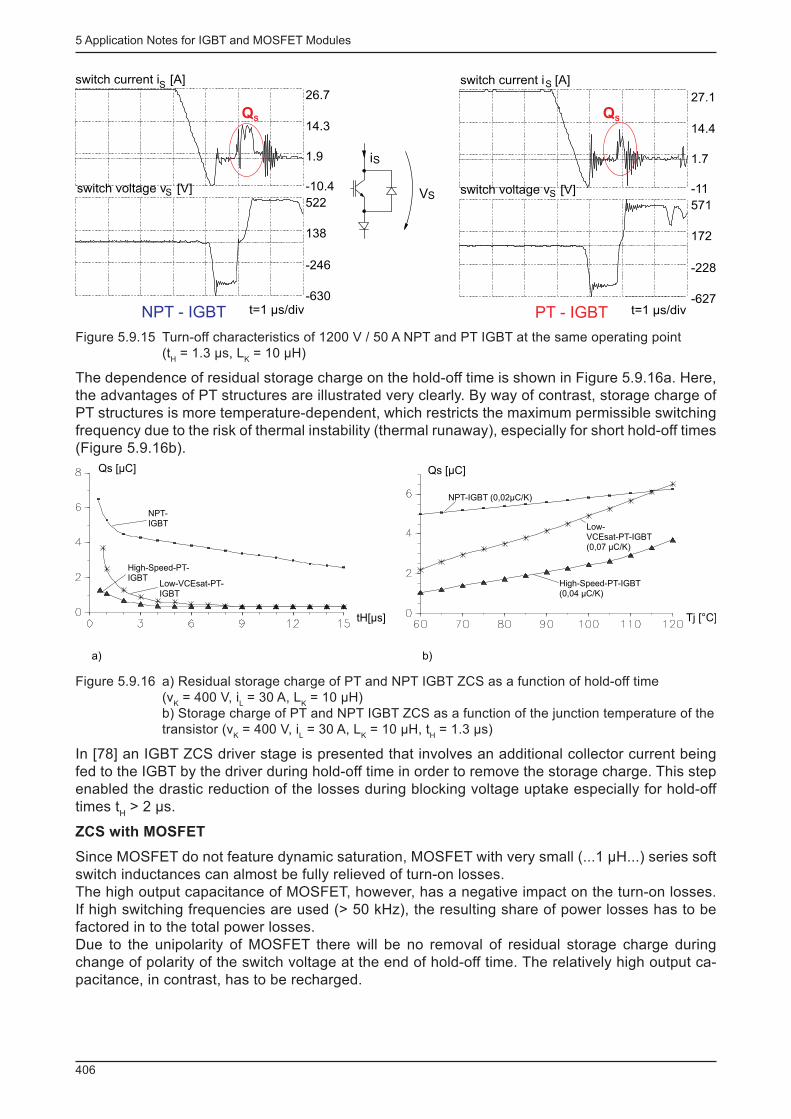
5 Application Notes for IGBT and MOSFET Modules
406
switch current i [A]S
26.7
14.3
1.9
-10.4
522
138
-246
-630
switch voltage v [V]S
t=1 µs/div
27.1
14.4
1.7
-11
571
172
-228
-627t=1 µs/div
switch current i [A]S
switch voltage v [V]S
PT - IGBTNPT - IGBT
V
iS
S
QS QS
Figure 5.9.15 Turn-off characteristics of 1200 V / 50 A NPT and PT IGBT at the same operating point (t
H = 1.3 µs, L
K = 10 µH)
The dependence of residual storage charge on the hold-off time is shown in Figure 5.9.16a. Here, the advantages of PT structures are illustrated very clearly. By way of contrast, storage charge of PT structures is more temperature-dependent, which restricts the maximum permissible switching frequency due to the risk of thermal instability (thermal runaway), especially for short hold-off times (Figure 5.9.16b).
Qs [µC]
NPT-IGBT
High-Speed-PT-IGBT
Low-VCEsat-PT-IGBT
tH[µs]
Qs [µC]
Tj [°C]
NPT-IGBT (0,02µC/K)
Low-VCEsat-PT-IGBT(0,07 µC/K)
High-Speed-PT-IGBT(0,04 µC/K)
a) b)
Figure 5.9.16 a) Residual storage charge of PT and NPT IGBT ZCS as a function of hold-off time (v
K = 400 V, i
L = 30 A, L
K = 10 µH)
b) Storage charge of PT and NPT IGBT ZCS as a function of the junction temperature of the transistor (v
K = 400 V, i
L = 30 A, L
K = 10 µH, t
H = 1.3 µs)
In [78] an IGBT ZCS driver stage is presented that involves an additional collector current being fed to the IGBT by the driver during hold-off time in order to remove the storage charge. This step enabled the drastic reduction of the losses during blocking voltage uptake especially for hold-off times t
H > 2 µs.
ZCS with MOSFET
Since MOSFET do not feature dynamic saturation, MOSFET with very small (...1 µH...) series soft switch inductances can almost be fully relieved of turn-on losses.The high output capacitance of MOSFET, however, has a negative impact on the turn-on losses. If high switching frequencies are used (> 50 kHz), the resulting share of power losses has to be factored in to the total power losses.Due to the unipolarity of MOSFET there will be no removal of residual storage charge during change of polarity of the switch voltage at the end of hold-off time. The relatively high output ca-pacitance, in contrast, has to be recharged.

5 Application Notes for IGBT and MOSFET Modules
407
Fast diodes in ZCS
In ZCS mode, diodes turn off with reverse-recovery di/dt and take up reverse blocking voltage at the same time. Due to the existing commutation inductances, current will be commutated in the diodes at a lower speed than in hard-switching converters (lower reverse current peak, reduced turn-off losses). Nevertheless, the need for very good dynamic turn-off behaviour hand in hand with low turn-off losses prevails.
In addition, the use of fast diodes as series diodes of IGBT or MOSFET in ZCS mode calls for very good dynamic turn-on behaviour of the diodes (forward recovery).
5.9.3.4 Conclusion
The behaviour of power semiconductors during hard switching is not applicable to soft switching. In principle, components with a shorter charge carrier lifetime are more suitable for soft-switching applications due to the aforementioned dynamic processes. Generally speaking, the information on power electronic components specifi ed in existing datasheets is not suitable for evaluating dy-namic behaviour in ZVS and ZCS topologies.
Owing to the great variety of low-loss converter topologies with their own specifi c switch require-ments, a general conclusion on the limitation of frequencies of IGBT and MOSFET switches can-not be drawn.

5
408
6 Handling instructions and environmental conditions
409
6 Handling instructions and environmental conditions
This chapter provides an overview of the most important requirements for transportation, storage, mounting and operation of discrete power semiconductors and power modules. The requirements for transportation and storage also apply to modules integrated in devices in order to ensure reli-able operation throughout the device's service life.
6.1 Sensitivity to ESD and measures for protection
All IGBT or MOSFET power modules are sensitive to ESD ( E lectro S tatic D ischarge) due to the thickness of their gate isolation (gate oxide layer), which amounts to some ten nanometers only. This is why they are classifi ed as ESD ( E lectrostactic S ensitive D evices) in accordance with EN 61340-5-1 and EN 61340-2-3 – i.e. devices which are prone to damage by electrostatic fi elds or electrostatic discharge during routine handling, testing and transportation. IGBT and power MOS-FET with big chip areas are characterized by high input capacitances and, compared to small-signal devices, are classifi ed as minor sensitive components according to procedure 3015.6 of the MIL-STD 883C standard.
When handling IGBT or MOSFET power modules, the regulations set down in the aforementioned MIL standard, as well as those of DIN VDE 0843 T2, which is identical to IEC 801-2, must be ad-hered to. Inspection and further processing must always be carried out by suitably clothed staff (antistatic overalls, wrist strap, if available). Before ESD-sensitive components are processed, all transportation and assembly equipment, as well as PCBs must be adjusted to the potential of the ESD-sensitive components, and electrostatic re-charge must be prevented. For identifi cation pur-poses, a warning label as specifi ed in IEC 60417, reg. no. 5134 must be attached to packaging of electrostatic sensitive devices (Figure 6.1.1).
Figure 6.1.1 Warning label for ESD packaging
The power modules are supplied with gate and emitter / source terminals short-circuited by suit-able conductive packaging, packaging lined with conductive foam or rubber mats, self-sealing metal foils, with annular rivets on the terminals or caps on the connectors. If possible, this short circuit should not be removed until connecting the gate.
6.2 Ambient conditions for storage, transportation and operation
This sections refers to the classifi cation and description of environmental conditions according to EN 50178 and EN 60721-3 (IEC 721-3) including standard sections EN 60721-3-1 (storage), EN 60721-3-2 (transportation) and EN 60721-3-3 (stationary use at weather-protected locations). Other parts not referred to in this section describe the conditions of stationary use at non-weather-protected locations (EN 60721-3-4), ground vehicle installations (EN 60721-3-5), ship environ-ment (EN 60721-3-6) and portable, non-stationary installations.
As illustrated in Figure 6.2.1, devices are exposed to many different kinds of environmental stress, which are summarised accordingly in the environmental conditions stipulated in EN 60721-3. Envi-ronmental conditions which can be then expected to occur in the fi eld application must be factored in during the development and construction of electronic devices already. This also includes the selection of suitable power semiconductors, as well as semiconductor cooling and assembly.
Consequently, in order to comply with the environmental provisions determined by application specifi cs, operating location, the conditions of storage and transportation to the fi nal place of use, as well as conditions during down-time, the selection of components on the basis of environmental conditions is to be iteratively combined with design measures for protection from environmental impacts.

6 Handling instructions and environmental conditions
410
The best compromise between the component, circuitry and design complexity must be found during the development process already, while taking into consideration existing semiconductor-specifi c or component-specifi c limits such as moisture absorption of the soft mould of IGBT.
Stress
Mechanical Climatic Chemical Biological Others
Stacker pressure
Falling
Tilting
Overturning
Rebounding
Periodic vibrations
Stochastic vibrations
…
Sunrays
Temperature
Humidity
Air pressure
Wind
Rain
Hair-frost
Ice
Snow
Hail
Fog
…
Waste gases
Saline fog
Industrial
atmosphere
Pollutants
Mould
Fungus
Bacteria
Birds
Snakes
Rodents
Insects
…
Fire
Splash water
Sousing /
submerging
Overflowing
Sand
Dust
Electromagnetic
radiation
…
…
Figure 6.2.1 Environmental stress factors during transportation, storage and operation as per DIN-EN 60721-3
EN 60721-3, environmental conditions are categorised according to the "nAxY" environmental classifi cation code:
The fi rst digit (n) identifi es the area of application that the requirements defi ned by the subsequent digits apply to.
n: 1: Storage 2: Transportation 3: Operation
The fi rst capital letter (A) determines the type of environmental quantity the limits refer to.
A: K: Climatic; M: Mechanical; B: Biological; C: Chemically active substances; S: Mechanically active substances; Z: Other climatic conditions
The third digit (x) determines the limits of the environmental quantity under A
x: Numbering (in ascending order by degree of severity)
Y: Additional capital letter for further specifi cation
In most cases, higher degree classes include the requirements of lower degree classes. In addi-tion, assembly, maintenance and repair conditions are to be taken into account, insofar as these are likely to deviate from the storage and operating conditions. Furthermore, 7 standardized com-binations of the environmental conditions above (designated with "IExx“) are defi ned in the afore-mentioned EN standard, providing a thorough classifi cation description for 4 standard cases of environmental conditions with respective application examples.
Compliance with the specifi ed environmental requirements is proven by inspection and testing of sample products under simulated environmental conditions. To do so, the products are subjected to environmental tests that are set down in the IEC 60068-x-x and IEC 60749 standards. To select suitable test procedures and the degree of severity, the "Guide on the correlation and transforma-tion of environmental condition classes of IEC 60721-x to the environmental tests of IEC 60068" (draft standard DIN 40046-721-x, separate documentation for storage (-1), transportation (-2), stationary use at weather-protected locations (-3), etc.) may be referred to.
The following sections will provide a rough characterization of the most important environmental classes using the example of the operating conditions for electric appliances in stationary use at

6 Handling instructions and environmental conditions
411
weather-protected locations according to EN 60721-3-3. Detailed information on specifi c limits is provided in EN 60721-3-3. Please refer to this for a more thorough understanding of the classifi ca-tion system.
6.2.1 Climatic conditions
Climatic conditions include air temperature, absolute and relative air humidity, condensation, rate of temperature change, barometric pressure, solar and thermal radiation, air movement, wind-driven rain, water (except for rainfall) and ice formation.
Climatic conditions are classifi ed into 11 categories designated by codes 3K1....3K11, which are sorted in ascending order with reference to their degree of climatic impact. The most important climate classes are: - 3K1: Fully air-conditioned locations. Locations with permanent air humidity and temperature regulation.
- 3K2: Closed locations with permanent air temperature regulation, non-regulated air humidity, condensation ruled out.
- 3K3: Closed locations with air temperature regulation, non-regulated air humidity, condensation ruled out.
- 3K4: Closed locations with air temperature regulation and a wide range of possible relative humidity (non-regulated air humidity). Products are able to withstand condensation and water (except for rainfall) impact.
- 3K5: Closed locations without air temperature or humidity regulation. Heating may be used if the climate class conditions differ greatly from the open-air climate. Products are able to withstand ice formation.
- 3K6, 3K7, 3K8: Weather-protected locations with optional openings to the open air, i.e. locations may only be partly closed.
Products (except for class 3K7L products) may be exposed to solar radiation of varying intensity. Impact from wind-driven precipitation (including snowfall) is permitted to a limited extent only. With the exception of class 3K1, the climate classes correlate with the open-air climate types as per EN 60721-2-1: - extremely cold climate (except for the Antarctic) - cold climate - moderate climate - moderately dry climate - dry-hot climate - extremely dry-hot climate - moist-hot climate - moderately moist-hot climate
The climate class applicable to the individual open-air climates and operating conditions may therefore be determined using appendix A of the EN 60721-3-3 standard and the climatograms provided in the standard (also refer to the example in chapter 6.2.7).
6.2.2 Mechanical environmental conditions
Figure 6.2.2 illustrates the various types of mechanical stress listed in the environmental condi-tions in accordance with EN 60721-3-3.
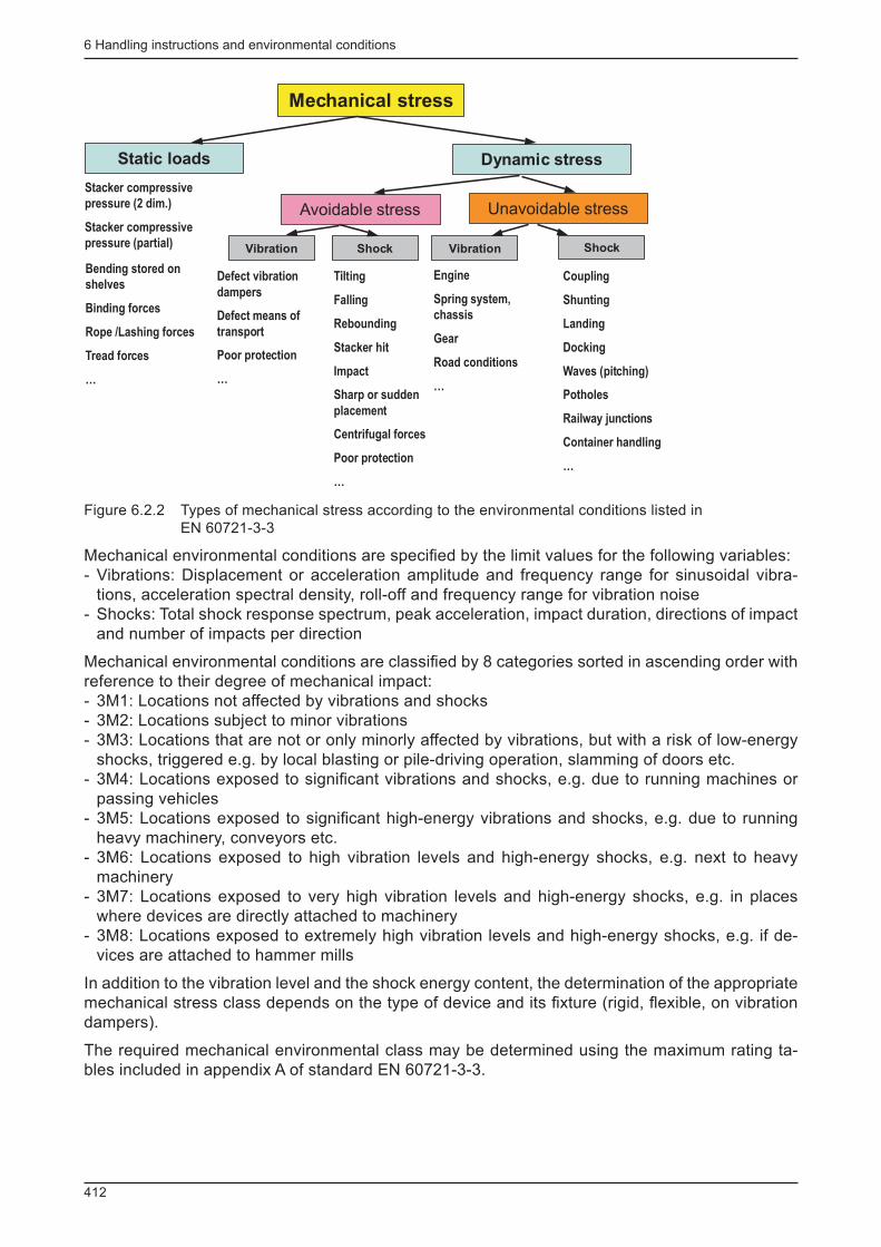
6 Handling instructions and environmental conditions
412
Mechanical stress
Static loads Dynamic stress
Stacker compressive
pressure (2 dim.)
Stacker compressive
pressure (partial)
Avoidable stress Unavoidable stress
Shock Vibration Shock
Tilting
Falling
Rebounding
Stacker hit
Impact
Sharp or sudden
placement
Centrifugal forces
Poor protection
…
Engine
Spring system,
chassis
Gear
Road conditions
…
Coupling
Shunting
Landing
Docking
Waves (pitching)
Potholes
Railway junctions
Container handling
…
Bending stored on
shelves
Binding forces
Rope /Lashing forces
Tread forces
…
Vibration
Defect vibration
dampers
Defect means of
transport
Poor protection
…
Figure 6.2.2 Types of mechanical stress according to the environmental conditions listed in EN 60721-3-3
Mechanical environmental conditions are specifi ed by the limit values for the following variables: - Vibrations: Displacement or acceleration amplitude and frequency range for sinusoidal vibra-tions, acceleration spectral density, roll-off and frequency range for vibration noise
- Shocks: Total shock response spectrum, peak acceleration, impact duration, directions of impact and number of impacts per direction
Mechanical environmental conditions are classifi ed by 8 categories sorted in ascending order with reference to their degree of mechanical impact: - 3M1: Locations not affected by vibrations and shocks - 3M2: Locations subject to minor vibrations - 3M3: Locations that are not or only minorly affected by vibrations, but with a risk of low-energy shocks, triggered e.g. by local blasting or pile-driving operation, slamming of doors etc.
- 3M4: Locations exposed to signifi cant vibrations and shocks, e.g. due to running machines or passing vehicles
- 3M5: Locations exposed to signifi cant high-energy vibrations and shocks, e.g. due to running heavy machinery, conveyors etc.
- 3M6: Locations exposed to high vibration levels and high-energy shocks, e.g. next to heavy machinery
- 3M7: Locations exposed to very high vibration levels and high-energy shocks, e.g. in places where devices are directly attached to machinery
- 3M8: Locations exposed to extremely high vibration levels and high-energy shocks, e.g. if de-vices are attached to hammer mills
In addition to the vibration level and the shock energy content, the determination of the appropriate mechanical stress class depends on the type of device and its fi xture (rigid, fl exible, on vibration dampers).
The required mechanical environmental class may be determined using the maximum rating ta-bles included in appendix A of standard EN 60721-3-3.

6 Handling instructions and environmental conditions
413
6.2.3 Biological environmental conditions
Biological environmental conditions are classifi ed by 3 categories sorted in ascending order ac-cording to the degree of contamination by mould / fungus formation, rodents and other animal pests: - 3B1: Locations not explicitly exposed to detrimental biological impact; mould formation or detri-ment due to animal pests, for example, are unlikely
- 3B2: Locations with a risk of mould formation and infestation by animal pests (with the exception of termites)
- 3B3: Locations with a risk of mould formation and infestation by animal pests, including termites
The required biological environmental class may be determined using the maximum rating tables included in appendix A of standard EN 60721-3-3.
6.2.4 Environmental impact due to chemically active substances
Impact caused by chemically active substances such as sea salt / road salt, sulphur dioxide, hydrogen sulphide, chlorine, hydrogen chloride, hydrogen fl uoride, ammonia, ozone and nitrous gases are classifi ed according to 6 categories arranged in ascending order with reference to their degree of environmental impact. - 3C1R: Locations with thorough atmosphere control and monitoring (cleanroom category) - 3C1L: Locations with continuous atmospheric control - 3C1: Locations with little industry and moderate traffi c density; higher risk of air pollution in more densely populated areas in winter due to heating; risk of salt spray in coastal regions and at non-fully-enclosed locations at sea
- 3C2: Locations with air pollution levels typical of more densely populated areas with industrial facilities and high traffi c volumes
- 3C3: Locations in the direct vicinity of industrial facilities with chemical emissions - 3C4: Locations within industrial facilities where emissions containing high concentrations of chemical pollutants are permissible.
The standard does not take into account chemically active liquids and other existing chemically active solids. The required chemical environmental class can be determined from the tables of maximum ratings included in appendix A of standard EN 60721-3-3.
6.2.5 Environmental impact caused by mechanically active substances
Impact caused by mechanically active substances such as sand particles in the air and dust par-ticles in air or precipitation are classifi ed into 4 categories arranged in ascending order with refer-ence to their degree of environmental impact: - 3S1: Locations with minimum dust formation; sand ingression is prevented - 3S2: Locations where no particular measures are taken to minimise dust formation or sand in-gression, but which are not situated near to dust or sand sources
- 3S3: Locations where no particular measures are taken to minimise dust formation or sand in-gression and which are situated near to dust or sand sources
- 3S4: Locations subject to sand or dust due to technical processes or situated in geographic re-gions with a permissible naturally high sand or dust concentration in the air
The required mechanical environmental class can be determined from the tables of maximum rat-ings included in appendix A of standard EN 60721-3-3.

6 Handling instructions and environmental conditions
414
6.2.6 Notes on operation at high altitudes
Depending on the particular circuit design, it might be necessary to limit the operating area when operating systems at heights greater than 2,000 m above sea level. - Reduction of the output power or maximum operating temperature of air-cooled systems due to the low atmospheric density and barometric pressure, which adversely affects the cooling sys-tem; cf. chapter 5.3
- Reduction of the insulation capacity, because the dielectric strength of the air decreases in line with the increase in assembly height (decreasing barometric pressure)
Most SEMIKRON power modules comply with EN 50178 as far as insulation distances (clearances and creepage distances) are concerned. For assembly heights higher than 2000 m above sea level, however, stricter clearance requirements apply. In this case, clearances should be increased by a correction factor or, if this is not feasible, upstream transformers could be used, for example, to reduce the line voltage. The particular correction factors are stipulated below according to IEC 60664-1, Table A.2.
Operating height (in metres)
above sea level
Barometric pressure in kPa Correction factor
2,000 82 1.00
2,500 76 1.075
3,000 70 1.14
4,000 62 1.29
5,000 50 1.48
Table 6.2.1 Effect of operating height on insulation distances
Example SKiiP3, 1700 V:
For appliances supplied with V N = 690 V
eff phase-to-phase voltage with grounded neutral point, the
minimum clearance for safe insulation up to 2,000 m above sea level is 8 mm (EN 50178, Table 3). At operating heights above 2,000 m, this clearance must be multiplied by the respective correction factor. As the clearance is 9 mm for SKiiP3 (= 1.125 x 8 mm), the component may be operated at heights of up to 2,880 m (correction factor approximated between 2,500 m and 3,000 m).
Infl uence of cosmic radiation on the failure rate
Cosmic radiation is high-energy particle radiation from outer space. Primary radiation consists mainly of electrons and fully ionised atoms penetrating the Earth's atmosphere. Primary radiation is emitted mainly by supernovas and by the sun as well. The Earth's outer atmosphere is exposed to around 1,000 particles per square meter and second, but only a very small portion of this reach-es the Earth's surface directly, since most primary particles collide with the gas molecules of the Earth's atmosphere (O
2 , N
2 ). The secondary particles generated in this process once again collide
with gas molecules in the Earth's atmosphere, causing them to disintegrate into a vast number of even smaller particles (pions, muons and neutrons), also referred to as cosmic ray shower, cf. Figure 6.2.3).
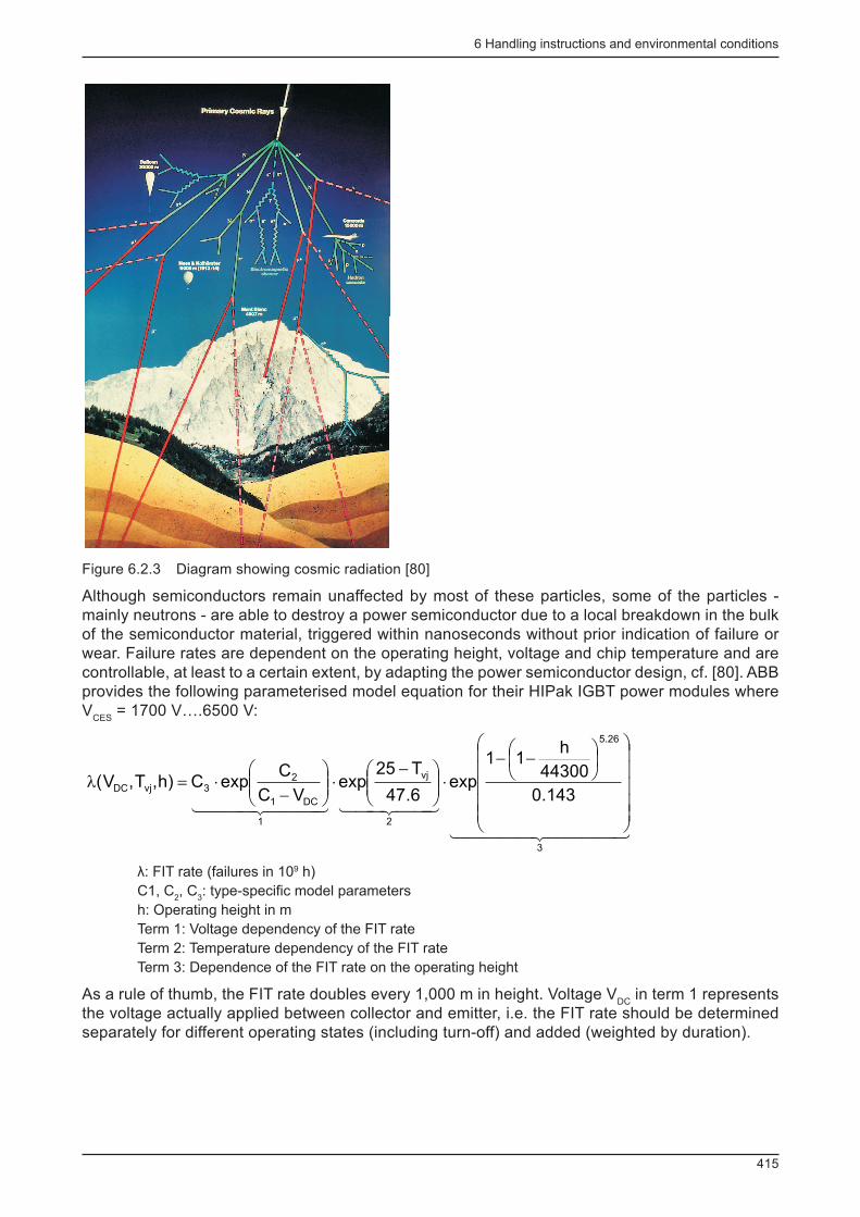
6 Handling instructions and environmental conditions
415
Figure 6.2.3 Diagram showing cosmic radiation [80]
Although semiconductors remain unaffected by most of these particles, some of the particles - mainly neutrons - are able to destroy a power semiconductor due to a local breakdown in the bulk of the semiconductor material, triggered within nanoseconds without prior indication of failure or wear. Failure rates are dependent on the operating height, voltage and chip temperature and are controllable, at least to a certain extent, by adapting the power semiconductor design, cf. [80]. ABB provides the following parameterised model equation for their HIPak IGBT power modules where V
CES = 1700 V….6500 V:
4444 34444 21
44 344 21444 3444 21
3
26.5
2
vj
1
DC1
23vjDC
143.0
44300
h11
exp6.47
T25exp
VC
CexpC)h,T,V(
÷÷÷÷÷
ø
ö
ççççç
è
æ÷øö
çèæ --
×÷÷ø
öççè
æ -×÷÷
ø
öççè
æ-
×=l
λ: FIT rate (failures in 109 h) C1, C
2 , C
3 : type-specifi c model parameters
h: Operating height in m Term 1: Voltage dependency of the FIT rate Term 2: Temperature dependency of the FIT rate Term 3: Dependence of the FIT rate on the operating height
As a rule of thumb, the FIT rate doubles every 1,000 m in height. Voltage V DC
in term 1 represents the voltage actually applied between collector and emitter, i.e. the FIT rate should be determined separately for different operating states (including turn-off) and added (weighted by duration).

6 Handling instructions and environmental conditions
416
6.2.7 Air humidity limits and condensation protection
Silicone-based single-layer coating and encapsulation systems have become increasingly used to provide electrical insulation on the surface of DBC substrates. This is done for numerous reasons, e.g. polluting environment in production, recyclability, minimisation of mechanical stress, weight reduction.
Different humidity levels are balanced in both directions within these encapsulating systems. Thus, the speed of diffusion of water ions in the silicone gel amounts to 0.04 mm/s at 18°C, increasing up to 1 mm/s at 100°C. For silicon layers of approx. 5 mm in thickness, the saturation state is reached within 5 hours.
Example SKiiP3:
A time constant of τ = 8 h, the residual moisture left in the silicone gel after 4 hours of drying time is 40%.
Basically, the accumulation of water ions induces changes in the fi eld line patterns in the barrier layers between semiconductor and casting compound, as well as in the fotoimide insulation layer of the chips. Electrolytic processes may be involved as well. Most SEMIKRON power modules conform to climate class 3K3 as per EN 60721-3-3 in compliance with EN 50178 and, with regard to clearances and creepage distances, may be operated under pollution degree 2 conditions stipu-lated by EN 50178 and EN 61800-5-1.
Accordingly, operation is not permitted in places of operation or installation where dripping or condensation water impacts on the power modules for example. Condensation is admissible oc-casionally only, and on provision that the system is not under voltage. Under no circumstances may condensation residue resulting from occasional condensation be allowed to accumulate due to frequent condensation / drying cycles.
To prevent power semiconductor failure due to condensation, applications must comply with the component-specifi c climatic requirements. For operation, additional anti-condensation measures such as standstill heating, air conditioning, continuous duty, cooling water temperature control etc., must be taken. According to climate class 3K3, operation must take place in shielded locations which must not be exposed to weather and which have a maximum relative air humidity of 85% and an absolute air humidity of 26 g/m³. Interpreting the climatogram in Figure 6.2.4, this means that at an air temperature of 40°C, for example, the relative air humidity must not exceed 50%.
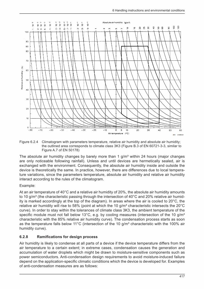
6 Handling instructions and environmental conditions
417
Figure 6.2.4 Climatogram with parameters temperature, relative air humidity and absolute air humidity; the outlined area corresponds to climate class 3K3 (Figure B.3 of EN 60721-3-3, similar to Figure A.7 of EN 50178)
The absolute air humidity changes by barely more than 1 g/m³ within 24 hours (major changes are only noticeable following rainfall). Unless and until devices are hermetically sealed, air is exchanged with the environment. Consequently, the absolute air humidity inside and outside the device is theoretically the same. In practice, however, there are differences due to local tempera-ture variations, since the parameters temperature, absolute air humidity and relative air humidity interact according to the rules of the climatogram.
Example:
At an air temperature of 40°C and a relative air humidity of 20%, the absolute air humidity amounts to 10 g/m³ (the characteristic passing through the intersection of 40°C and 20% relative air humid-ity is marked accordingly at the top of the diagram). In areas where the air is cooled to 20°C, the relative air humidity will rise to 58% (point at which the 10 g/m³ characteristic intersects the 20°C curve). In order to stay within the tolerances of climate class 3K3, the ambient temperature of the specifi c module must not fall below 13°C, e.g. by cooling measures (intersection of the 10 g/m³ characteristic with the 85% relative air humidity curve). The condensation process starts as soon as the temperature falls below 11°C (intersection of the 10 g/m³ characteristic with the 100% air humidity curve).
6.2.8 Ramifi cations for design process
Air humidity is likely to condense at all parts of a device if the device temperature differs from the air temperature to a certain extent; in extreme cases, condensation causes the generation and accumulation of water droplets which might be drawn to moisture-sensitive components such as power semiconductors. Anti-condensation design requirements to avoid moisture-induced failure depend on the application-specifi c climatic conditions which the device is developed for. Examples of anti-condensation measures are as follows:

6 Handling instructions and environmental conditions
418
a) Case with separate internal air circulation - closed system (min. protection degree IP65) with an air-to-air or water-to-air heat exchanger - closed system with internal air conditioning (air temperature and air humidity regulation) - open system with in-case forced ventilation
Power semiconductors integrated in such systems are usually liquid-cooled or cooled by heat sinks located outside the case and separated by a seal.
b) Heat sink temperature control using cooling-air intake control (fan speed or fan duty cycle)
c) Internal temperature control using interior heating
The diagram in Figure 6.2.5 illustrates the relevant design features with the example of a switch-gear cabinet with integrated SKiiP power modules.
Figure 6.2.5 Design details of a power electronic switchgear cabinet1. Power module to be protected from moisture2. Critical zone: Heat sink, heat sink temperature T1, e.g. adjustable with a two-step controller to T1 ≥ T2 → Risk of condensation, if T1 < T23. Heating: Interior temperature is adjusted to T2 within the admissible operating temperature range of the components4. Cooling-air intake to the switchgear cabinet (air fl ow and air humidity control)5. Air intake and outlet: Possible chimney effects must be attenuated by way of air channelling to make sure that the cooling air is evenly distributed 6. Case with IP54 protection min.7. Defl ection of water droplets from the case top8. Optional: Water-absorbing granulate for passive air humidity control 9. Critical zones: Cabinet side panels
In a closed case, surfaces that are colder than the interior air temperature are likely to be affected by condensation or even ice formation. Condensation water is typically generated if the tempera-ture of the interior environment drops to a point where the relative air humidity reaches 100%. The air humidity will then condensate on surfaces with temperatures below the interior temperature (e.g. air intake and outlet, case panels, heat sink). The requirements for ventilation inside the de-vice depend on the respective climatic conditions of use.
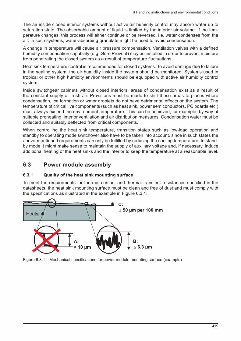
6 Handling instructions and environmental conditions
419
The air inside closed interior systems without active air humidity control may absorb water up to saturation state. The absorbable amount of liquid is limited by the interior air volume. If the tem-perature changes, this process will either continue or be reversed, i.e. water condenses from the air. In such systems, water-absorbing granulate might be used to avoid condensation.
A change in temperature will cause air pressure compensation. Ventilation valves with a defi ned humidity compensation capability (e.g. Gore Prevent) may be installed in order to prevent moisture from penetrating the closed system as a result of temperature fl uctuations.
Heat sink temperature control is recommended for closed systems. To avoid damage due to failure in the sealing system, the air humidity inside the system should be monitored. Systems used in tropical or other high humidity environments should be equipped with active air humidity control system.
Inside switchgear cabinets without closed interiors, areas of condensation exist as a result of the constant supply of fresh air. Provisions must be made to shift these areas to places where condensation, ice formation or water droplets do not have detrimental effects on the system. The temperature of critical live components (such as heat sink, power semiconductors, PC boards etc.) must always exceed the environment temperature. This can be achieved, for example, by way of suitable preheating, interior ventilation and air distribution measures. Condensation water must be collected and suitably defl ected from critical components.
When controlling the heat sink temperature, transition states such as low-load operation and standby to operating mode switchover also have to be taken into account, since in such states the above-mentioned requirements can only be fulfi lled by reducing the cooling temperature. In stand-by mode it might make sense to maintain the supply of auxiliary voltage and, if necessary, induce additional heating of the heat sinks and the interior to keep the temperature at a reasonable level.
6.3 Power module assembly
6.3.1 Quality of the heat sink mounting surface
To meet the requirements for thermal contact and thermal transient resistances specifi ed in the datasheets, the heat sink mounting surface must be clean and free of dust and must comply with the specifi cations as illustrated in the example in Figure 6.3.1:
A:
> 10 µm
B:
6.3 µm£
Heatsink
C:
50 µm per 100 mm£
Figure 6.3.1 Mechanical specifi cations for power module mounting surface (example)
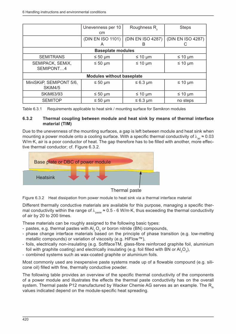
6 Handling instructions and environmental conditions
420
Unevenness per 10 cm
Roughness R z
Steps
(DIN EN ISO 1101)A
(DIN EN ISO 4287)B
(DIN EN ISO 4287)C
Baseplate modules
SEMITRANS ≤ 50 μm ≤ 10 μm ≤ 10 μm
SEMIPACK, SEMiX, SEMIPONT…4
≤ 50 μm ≤ 10 μm ≤ 10 μm
Modules without baseplate
MiniSKiiP, SEMIPONT 5/6, SKiM4/5
≤ 50 μm ≤ 6.3 μm ≤ 10 μm
SKiM63/93 ≤ 50 μm ≤ 10 μm ≤ 10 μm
SEMITOP ≤ 50 μm ≤ 6.3 μm no steps
Table 6.3.1 Requirements applicable to heat sink / mounting surface for Semikron modules
6.3.2 Thermal coupling between module and heat sink by means of thermal interface
material (TIM)
Due to the unevenness of the mounting surfaces, a gap is left between module and heat sink when mounting a power module onto a cooling surface. With a specifi c thermal conductivity of λ
air ≈ 0.03
W/m·K, air is a poor conductor of heat. The gap therefore has to be fi lled with another, more effec-tive thermal conductor; cf. Figure 6.3.2.
Thermal paste
Heatsink
Base plate or DBC of power module
Figure 6.3.2 Heat dissipation from power module to heat sink via a thermal interface material
Different thermally conductive materials are available for this purpose, managing a specifi c ther-mal conductivity within the range of λ
paste ≈ 0.5 - 6 W/m·K, thus exceeding the thermal conductivity
of air by 20 to 200 times.
These materials can be roughly assigned to the following basic types: - pastes, e.g. thermal pastes with Al
2 O
3 or boron nitride (BN) compounds,
- phase change interface materials based on the principle of phase transition (e.g. low-melting metallic compounds) or variation of viscosity (e.g. HiFlow™),
- foils, electrically non-insulating (e.g. SoftfaceTM, glass-fi bre reinforced graphite foil, aluminium foil with graphite coating) and electrically insulating (e.g. foil fi lled with BN or Al
2 O
3 ),
- combined systems such as wax-coated graphite or aluminium foils.
Most commonly used are inexpensive paste systems made up of a fl owable compound (e.g. sili-cone oil) fi lled with fi ne, thermally conductive powder.
The following table provides an overview of the specifi c thermal conductivity of the components of a power module and illustrates the effects the thermal paste conductivity has on the overall system. Thermal paste P12 manufactured by Wacker Chemie AG serves as an example. The R
th
values indicated depend on the module-specifi c heat spreading.
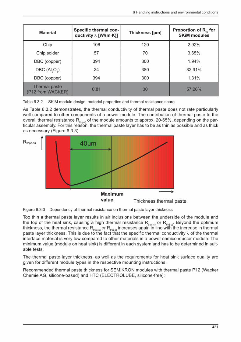
6 Handling instructions and environmental conditions
421
Material Specifi c thermal con-
ductivity λ [W/(m·K)] Thickness [µm]
Proportion of R th for
SKiM modules
Chip 106 120 2.92%
Chip solder 57 70 3.65%
DBC (copper) 394 300 1.94%
DBC (Al 2 O
3 ) 24 380 32.91%
DBC (copper) 394 300 1.31%
Thermal paste (P12 from WACKER)
0.81 30 57.26%
Table 6.3.2 SKiM module design: material properties and thermal resistance share
As Table 6.3.2 demonstrates, the thermal conductivity of thermal paste does not rate particularly well compared to other components of a power module. The contribution of thermal paste to the overall thermal resistance R
th(j-s) of the module amounts to approx. 20-65%, depending on the par-
ticular assembly. For this reason, the thermal paste layer has to be as thin as possible and as thick as necessary (Figure 6.3.3).
Rth(c-s)
Thickness thermal paste
Maximum
value
40µm
Figure 6.3.3 Dependency of thermal resistance on thermal paste layer thickness
Too thin a thermal paste layer results in air inclusions between the underside of the module and the top of the heat sink, causing a high thermal resistance R
th(c-s) or R
th(j-s) . Beyond the optimum
thickness, the thermal resistance R th(c-s)
or R th(j-s)
increases again in line with the increase in thermal paste layer thickness. This is due to the fact that the specifi c thermal conductivity λ of the thermal interface material is very low compared to other materials in a power semiconductor module. The minimum value (module on heat sink) is different in each system and has to be determined in suit-able tests.
The thermal paste layer thickness, as well as the requirements for heat sink surface quality are given for different module types in the respective mounting instructions.
Recommended thermal paste thickness for SEMIKRON modules with thermal paste P12 (Wacker Chemie AG, silicone-based) and HTC (ELECTROLUBE, silicone-free):

6 Handling instructions and environmental conditions
422
Baseplate modules
SEMIPACK approx. 50 μm
SEMITRANS approx. 50 μm
SEMiX50…approx. 100 μm
SEMIPONT4 approx. 50 μm
Modules without baseplate
MiniSKiiP025…40 μm
MiniSKiiP135…50 μm
MiniSKiiP265…85 μm
MiniSKiiP345…65 μm
SEMIPONT5/650…55 μm
SKiM4/540...60 μm
SKiM63/9330…50 μm
SEMITOP120…25 μm
SEMITOP130…35 μm
SEMITOP350…55 μm
SEMITOP450…55 μm
Table 6.3.3 Recommended thermal paste layer thicknesses for Semikron modules
The specifi c thermal conductivity λ of P12 thermal paste recommended by SEMIKRON is at the lower end of the scale. The use of this particular thermal paste is recommended for the following reasons: - R
th test series have proven that the thermal conductivity of a thermal paste in actual application
depends not only on its thermal conductivity λ, but also on its specifi c composition. The larger the fi ller particles in a thermal paste, the higher the specifi c thermal conductivity. The particle size of the fi ller determines the minimum thermal layer thickness. In other words, the thermal paste layer applied cannot be thinner than the largest particles in the paste. After several temperature cycles, a paste with small particles (e.g. P12: particle size 0.04…4 µm) provides almost metal-to-metal contact at points where the contact pressure is particularly high, usually resulting in a substantial reduction in R
th(c-s) or R
th(j-s) .
- The paste is highly resistant to "bleeding" and "drying out".
The following table illustrates the properties of the most important thermal interface materials which have undergone testing at SEMIKRON.
Product
name;
manufac-
turer
Description Containing
silicone
Conductive Methods of
application
Applicable
thickness
of TIM in
µm
Thermal
resistance
Specifi c
thermal
conductiv-
ity λ W/
(m*K) (da-
tasheet)
P12, Wacker Paste, fi ller: Al
2 O
3
Yes No Rolling, screen / stencil print-ing
10-100 + 0.81
HTC, Elec-trolube
Paste, fi ller: Al
2 O
3
No No Rolling, screen / stencil print-ing
10-100 + 0.9
PSX-P8, Hala Contec GmbH
Phase changer, fi ller: aluminium powder
No No Rolling, screen / stencil print-ing
10-100 + 3.4
Keratherm 86/50; Kerafoil
Foil, fi ller: boron nitride
Yes No Manually 120 - 2.9
Q2 Pad; Bergquist
Aluminium foil with graphite coating
Yes Yes Manually 152 - 2.5

6 Handling instructions and environmental conditions
423
Product
name;
manufac-
turer
Description Containing
silicone
Conductive Methods of
application
Applicable
thickness
of TIM in
µm
Thermal
resistance
Specifi c
thermal
conductiv-
ity λ W/
(m*K) (da-
tasheet)
TIC 1000 A, Bergquist
Paste, fi ller: Al
2 O
3
Yes Yes Rolling, screen / stencil print-ing
15-100 O 1.5
TIC 4000, Bergquist
Paste, fi ller: fl uid metal
Yes yes Rolling, screen / stencil print-ing
approx. 100 + 4.0
KU ALC-5, Kunze
Phase-change aluminium foil with wax coating
No Yes Manually approx. 76 O 220
KU ALF; Kunze
Phase-change aluminium foil with wax and graphite coating
No Yes Manually approx. 76 + 220
Table 6.3.4 Types and properties of TIMs (thermal pastes and others)
Methods of thermal paste application
In addition to compliance with the recommended layer thicknesses, care must also be taken to ensure that the thermal paste is applied evenly and homogeneously across the module underside or heat sink surface. Non-homogeneity of the thermal paste layer (in extreme cases: application of one or more thermal paste blobs) may either cause cracks in the DBC substrate or lead to lo-cal overheating at spots where air inclusions remain between module underside and heat sink surface. This is particularly true when mounting modules with no baseplate, since, in such cases, the heat sink serves almost exclusively as thermal capacitance to manage transient thermal loads.
Application using a rubber roller
Applying thermal paste with a rubber roller may lead to suffi cient results, provided the procedure is carried out by experienced professional and suitably trained staff. This process, however, in-volves shortcomings such as non-homogeneity, poor reproducibility and risk of contamination. An ultrathin layer of thermal paste must be applied homogeneously either to the module or the heat sink contact surface using a hard rubber roller. Layer thicknesses for the different SEMIKRON product groups are specifi ed in the table above.
Stencil and screen printing
In stencil printing, a stainless steel stencil and stainless steel scraper are normally used to print the thermal interface material on the module or heat sink. The "effective" thermal paste layer thick-ness is determined by the ratio of fi lled area to non-fi lled area, as well as by the height of the dots applied, which in turn is determined by the thickness of the stencil itself.
In screen printing, Monolen PET meshes and a polyurethane scraper with a shore hardness of 75 are commonly used. The thickness of the yarn and the number of yarns per unit of length deter-mine the thickness of the thermal paste layer.
In stencil and screen printing, far better results can be achieved than in the roller process, provided the printing is done automatically. Performing this process manually can lead to substantial proc-ess fl uctuations.
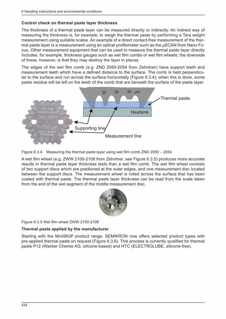
6 Handling instructions and environmental conditions
424
Control check on thermal paste layer thickness
The thickness of a thermal paste layer can be measured directly or indirectly. An indirect way of measuring the thickness is, for example, to weigh the thermal paste by performing a Tara weight measurement using suitable scales. An example of a direct contact-free measurement of the ther-mal paste layer is a measurement using an optical profi lometer such as the μSCAN from Nano Fo-cus. Other measurement equipment that can be used to measure the thermal paste layer directly includes, for example, thickness gauges such as wet fi lm combs or wet fi lm wheels; the downside of these, however, is that they may destroy the layer in places.
The edges of the wet fi lm comb (e.g. ZND 2050-2054 from Zehntner) have support teeth and measurement teeth which have a defi ned distance to the surface. The comb is held perpendicu-lar to the surface and run across the surface horizontally (Figure 6.3.4); when this is done, some paste residue will be left on the teeth of the comb that are beneath the surface of the paste layer.
Thermal paste
Supporting tine
Measurement tine
20 25 30 µm
Heatsink
Figure 6.3.4 Measuring the thermal paste layer using wet fi lm comb ZND 2050 – 2054
A wet fi lm wheel (e.g. ZWW 2100-2108 from Zehntner, see Figure 6.3.5) produces more accurate results in thermal paste layer thickness tests than a wet fi lm comb. The wet fi lm wheel consists of two support discs which are positioned at the outer edges, and one measurement disc located between the support discs. The measurement wheel is rolled across the surface that has been coated with thermal paste. The thermal paste layer thickness can be read from the scale taken from the end of the wet segment of the middle measurement disc.
Figure 6.3.5 Wet fi lm wheel ZWW 2100-2108
Thermal paste applied by the manufacturer
Starting with the MiniSKiiP product range, SEMIKRON now offers selected product types with pre-applied thermal paste on request (Figure 6.3.6). This process is currently qualifi ed for thermal paste P12 (Wacker Chemie AG, silicone-based) and HTC (ELECTROLUBE, silicone-free).
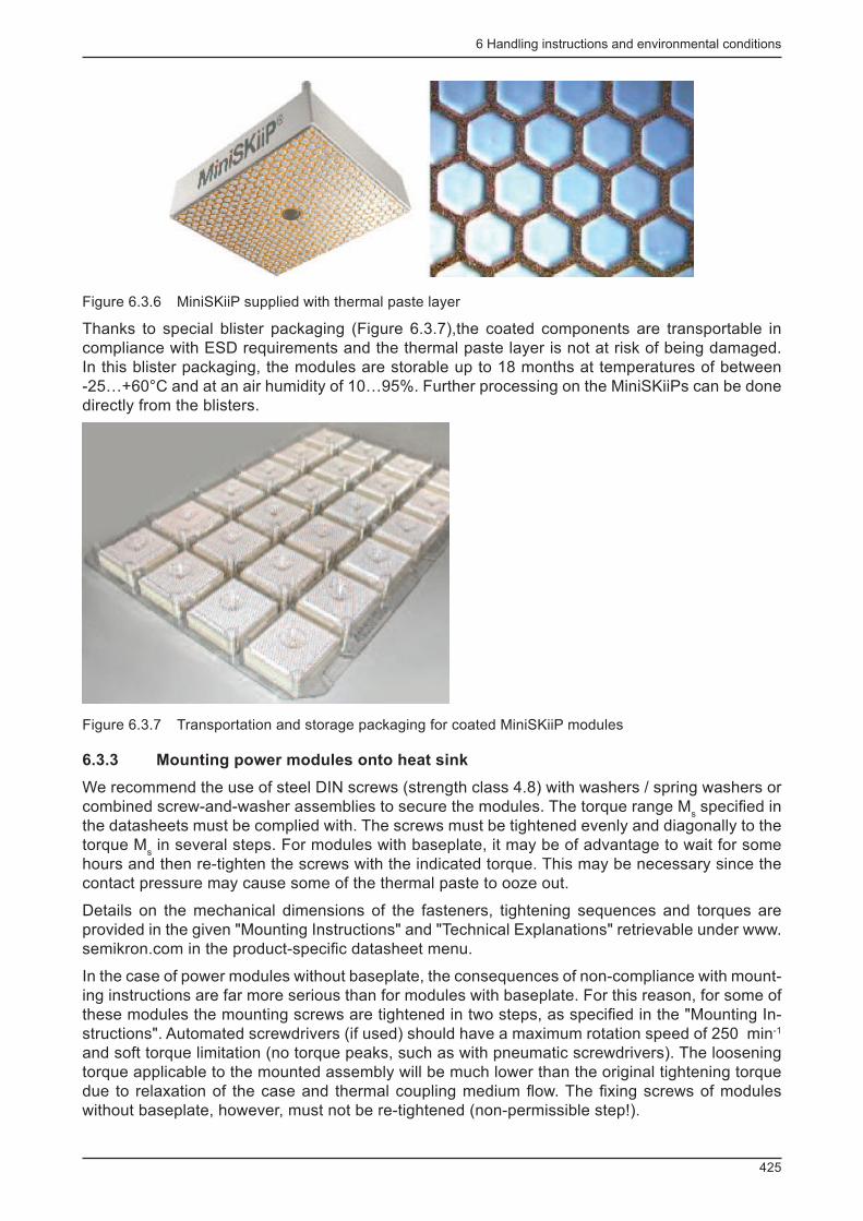
6 Handling instructions and environmental conditions
425
Figure 6.3.6 MiniSKiiP supplied with thermal paste layer
Thanks to special blister packaging (Figure 6.3.7),the coated components are transportable in compliance with ESD requirements and the thermal paste layer is not at risk of being damaged. In this blister packaging, the modules are storable up to 18 months at temperatures of between -25…+60°C and at an air humidity of 10…95%. Further processing on the MiniSKiiPs can be done directly from the blisters.
Figure 6.3.7 Transportation and storage packaging for coated MiniSKiiP modules
6.3.3 Mounting power modules onto heat sink
We recommend the use of steel DIN screws (strength class 4.8) with washers / spring washers or combined screw-and-washer assemblies to secure the modules. The torque range M
s specifi ed in
the datasheets must be complied with. The screws must be tightened evenly and diagonally to the torque M
s in several steps. For modules with baseplate, it may be of advantage to wait for some
hours and then re-tighten the screws with the indicated torque. This may be necessary since the contact pressure may cause some of the thermal paste to ooze out.
Details on the mechanical dimensions of the fasteners, tightening sequences and torques are provided in the given "Mounting Instructions" and "Technical Explanations" retrievable under www.semikron.com in the product-specifi c datasheet menu.
In the case of power modules without baseplate, the consequences of non-compliance with mount-ing instructions are far more serious than for modules with baseplate. For this reason, for some of these modules the mounting screws are tightened in two steps, as specifi ed in the "Mounting In-structions". Automated screwdrivers (if used) should have a maximum rotation speed of 250 min -1 and soft torque limitation (no torque peaks, such as with pneumatic screwdrivers). The loosening torque applicable to the mounted assembly will be much lower than the original tightening torque due to relaxation of the case and thermal coupling medium fl ow. The fi xing screws of modules without baseplate, however, must not be re-tightened (non-permissible step!).
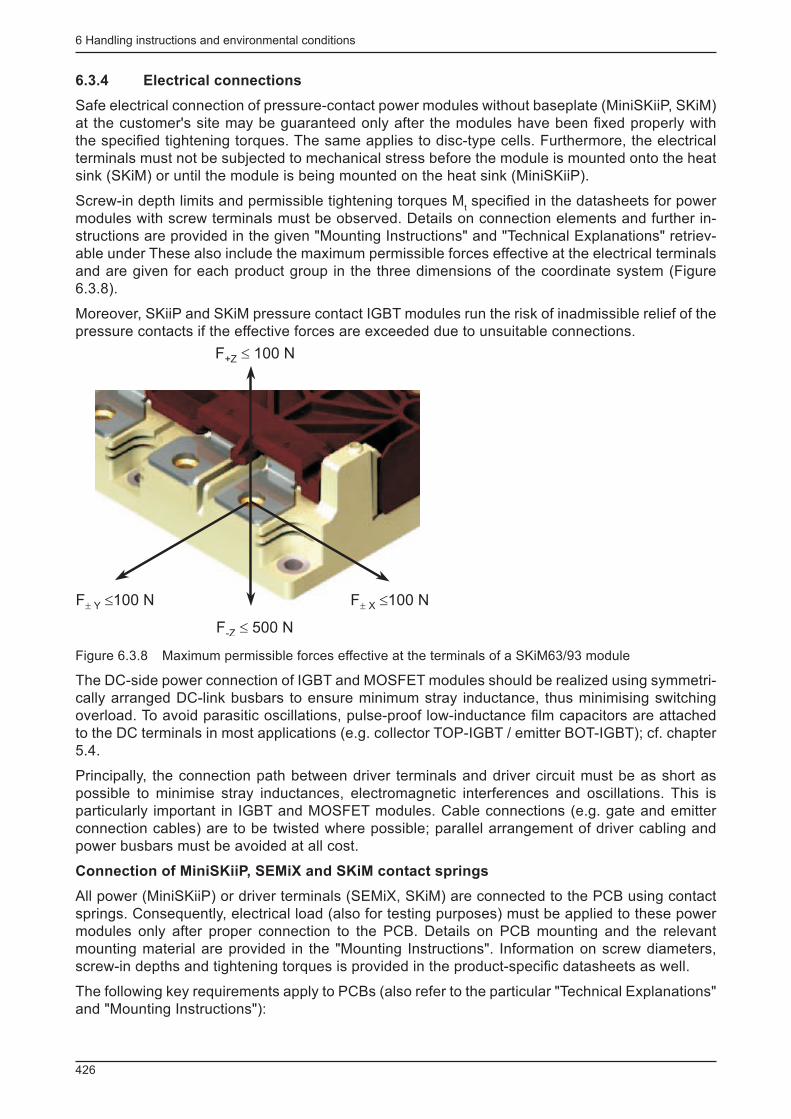
6 Handling instructions and environmental conditions
426
6.3.4 Electrical connections
Safe electrical connection of pressure-contact power modules without baseplate (MiniSKiiP, SKiM) at the customer's site may be guaranteed only after the modules have been fi xed properly with the specifi ed tightening torques. The same applies to disc-type cells. Furthermore, the electrical terminals must not be subjected to mechanical stress before the module is mounted onto the heat sink (SKiM) or until the module is being mounted on the heat sink (MiniSKiiP).
Screw-in depth limits and permissible tightening torques M t specifi ed in the datasheets for power
modules with screw terminals must be observed. Details on connection elements and further in-structions are provided in the given "Mounting Instructions" and "Technical Explanations" retriev-able under These also include the maximum permissible forces effective at the electrical terminals and are given for each product group in the three dimensions of the coordinate system (Figure 6.3.8).
Moreover, SKiiP and SKiM pressure contact IGBT modules run the risk of inadmissible relief of the pressure contacts if the effective forces are exceeded due to unsuitable connections.
F+Z £ 100 N
F-Z £ 500 N
F± X £100 NF± Y £100 N
Figure 6.3.8 Maximum permissible forces effective at the terminals of a SKiM63/93 module
The DC-side power connection of IGBT and MOSFET modules should be realized using symmetri-cally arranged DC-link busbars to ensure minimum stray inductance, thus minimising switching overload. To avoid parasitic oscillations, pulse-proof low-inductance fi lm capacitors are attached to the DC terminals in most applications (e.g. collector TOP-IGBT / emitter BOT-IGBT); cf. chapter 5.4.
Principally, the connection path between driver terminals and driver circuit must be as short as possible to minimise stray inductances, electromagnetic interferences and oscillations. This is particularly important in IGBT and MOSFET modules. Cable connections (e.g. gate and emitter connection cables) are to be twisted where possible; parallel arrangement of driver cabling and power busbars must be avoided at all cost.
Connection of MiniSKiiP, SEMiX and SKiM contact springs
All power (MiniSKiiP) or driver terminals (SEMiX, SKiM) are connected to the PCB using contact springs. Consequently, electrical load (also for testing purposes) must be applied to these power modules only after proper connection to the PCB. Details on PCB mounting and the relevant mounting material are provided in the "Mounting Instructions". Information on screw diameters, screw-in depths and tightening torques is provided in the product-specifi c datasheets as well.
The following key requirements apply to PCBs (also refer to the particular "Technical Explanations" and "Mounting Instructions"):
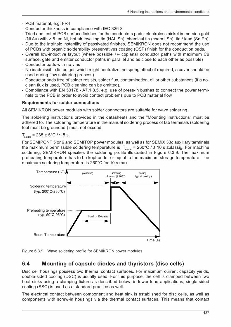
6 Handling instructions and environmental conditions
427
- PCB material, e.g. FR4 - Conductor thickness in compliance with IEC 326-3 - Tried and tested PCB surface fi nishes for the conductors pads: electroless nickel immersion gold (Ni Au) with > 5 μm Ni, hot air levelling tin (HAL Sn), chemical tin (chem.l Sn), tin / lead (Sn Pb)
- Due to the intrinsic instability of passivated fi nishes, SEMIKRON does not recommend the use of PCBs with organic solderability preservatives coating (OSP) fi nish for the conduction pads.
- Overall low-inductive layout (where possible +/- coplanar conductor paths with maximum Cu surface, gate and emitter conductor paths in parallel and as close to each other as possible)
- Conductor pads with no vias - No inadmissible tin bulges which might neutralize the spring effect (if required, a cover should be used during fl ow soldering process)
- Conductor pads free of solder resists, solder fl ux, contamination, oil or other substances (if a no-clean fl ux is used, PCB cleaning can be omitted).
- Compliance with EN 50178 - A7.1.8.5, e.g. use of press-in bushes to connect the power termi-nals to the PCB in order to avoid contact problems due to PCB material fl ow
Requirements for solder connections
All SEMIKRON power modules with solder connectors are suitable for wave soldering.
The soldering instructions provided in the datasheets and the "Mounting Instructions" must be adhered to. The soldering temperature in the manual soldering process of tab terminals (soldering tool must be grounded!) must not exceed
T solder
= 235 ± 5°C / ≤ 5 s.
For SEMIPONT 5 or 6 and SEMITOP power modules, as well as for SEMiX 33c auxiliary terminals the maximum permissible soldering temperature is T
solder = 260°C / ≤ 10 s zulässig. For machine
soldering, SEMIKRON specifi es the soldering profi le illustrated in Figure 6.3.9. The maximum preheating temperature has to be kept under or equal to the maximum storage temperature. The maximum soldering temperature is 260°C for 10 s max.
Figure 6.3.9 Wave soldering profi le for SEMIKRON power modules
6.4 Mounting of capsule diodes and thyristors (disc cells)
Disc cell housings possess two thermal contact surfaces. For maximum current capacity yields, double-sided cooling (DSC) is usually used. For this purpose, the cell is clamped between two heat sinks using a clamping fi xture as described below; in lower load applications, single-sided cooling (SSC) is used as a standard practice as well.
The electrical contact between component and heat sink is established for disc cells, as well as components with screw-in housings via the thermal contact surfaces. This means that contact
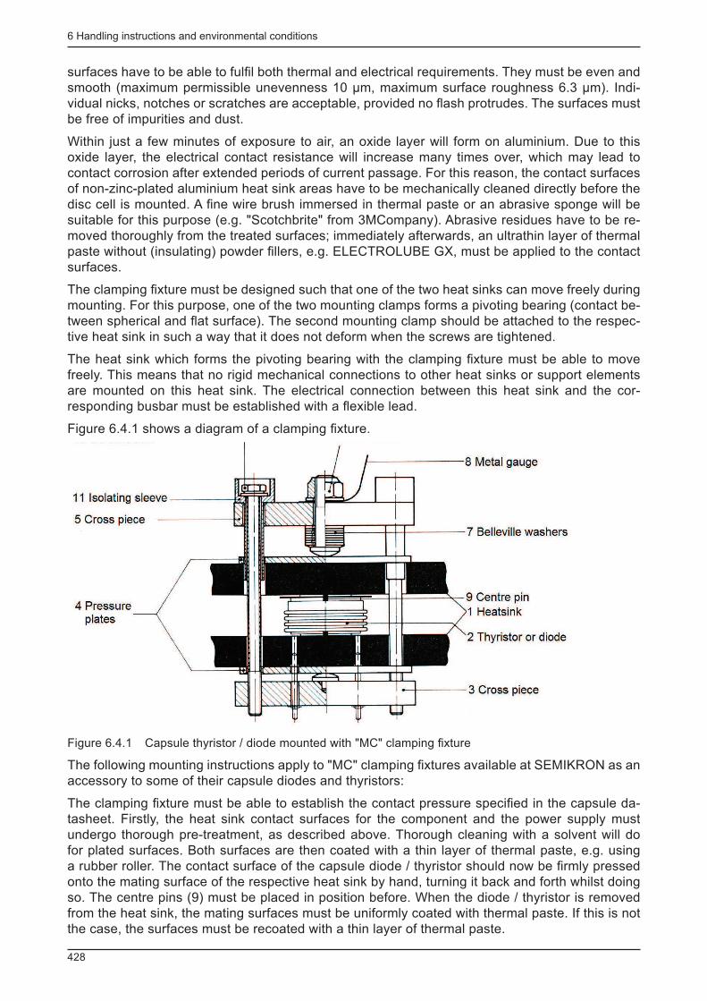
6 Handling instructions and environmental conditions
428
surfaces have to be able to fulfi l both thermal and electrical requirements. They must be even and smooth (maximum permissible unevenness 10 µm, maximum surface roughness 6.3 µm). Indi-vidual nicks, notches or scratches are acceptable, provided no fl ash protrudes. The surfaces must be free of impurities and dust.
Within just a few minutes of exposure to air, an oxide layer will form on aluminium. Due to this oxide layer, the electrical contact resistance will increase many times over, which may lead to contact corrosion after extended periods of current passage. For this reason, the contact surfaces of non-zinc-plated aluminium heat sink areas have to be mechanically cleaned directly before the disc cell is mounted. A fi ne wire brush immersed in thermal paste or an abrasive sponge will be suitable for this purpose (e.g. "Scotchbrite" from 3MCompany). Abrasive residues have to be re-moved thoroughly from the treated surfaces; immediately afterwards, an ultrathin layer of thermal paste without (insulating) powder fi llers, e.g. ELECTROLUBE GX, must be applied to the contact surfaces.
The clamping fi xture must be designed such that one of the two heat sinks can move freely during mounting. For this purpose, one of the two mounting clamps forms a pivoting bearing (contact be-tween spherical and fl at surface). The second mounting clamp should be attached to the respec-tive heat sink in such a way that it does not deform when the screws are tightened.
The heat sink which forms the pivoting bearing with the clamping fi xture must be able to move freely. This means that no rigid mechanical connections to other heat sinks or support elements are mounted on this heat sink. The electrical connection between this heat sink and the cor-responding busbar must be established with a fl exible lead.
Figure 6.4.1 shows a diagram of a clamping fi xture.
Figure 6.4.1 Capsule thyristor / diode mounted with "MC" clamping fi xture
The following mounting instructions apply to "MC" clamping fi xtures available at SEMIKRON as an accessory to some of their capsule diodes and thyristors:
The clamping fi xture must be able to establish the contact pressure specifi ed in the capsule da-tasheet. Firstly, the heat sink contact surfaces for the component and the power supply must undergo thorough pre-treatment, as described above. Thorough cleaning with a solvent will do for plated surfaces. Both surfaces are then coated with a thin layer of thermal paste, e.g. using a rubber roller. The contact surface of the capsule diode / thyristor should now be fi rmly pressed onto the mating surface of the respective heat sink by hand, turning it back and forth whilst doing so. The centre pins (9) must be placed in position before. When the diode / thyristor is removed from the heat sink, the mating surfaces must be uniformly coated with thermal paste. If this is not the case, the surfaces must be recoated with a thin layer of thermal paste.

6 Handling instructions and environmental conditions
429
The clamping fi xture is then positioned such that the cross piece (5) and pressure plate (4) with the tension bolts (10) is at the top. The cross piece (3) and pressure plate (4) is inserted from below, and the two tension bolts (10) are tightened alternately until a slight resistance is felt. Now check that both cross pieces (3) and (5) are parallel. To do so, it is suffi cient to measure the lengths of the ends of the bolts protruding from the bottom of the two cross pieces (3). The bolt ends must be equal in length. The two tension bolts (10) should now be tightened alternately up to the point where the metal gauge (8) can be easily moved. Under no circumstances should the tension bolts be tightened beyond this point, as doing so would mean that the permissible mounting force has been exceeded. For the same reason, the pre-set nut (6) of the Belleville washer assembly (7) should never be adjusted. The metal gauge (8) is secured to prevent it from falling out.
As an alternative to such clamping fi xtures, which may be installed by the customer, more simple mechanical clamping systems are used for the SEMISTACK product range (see chapter 5.5), which must be mounted in presses using force measuring devices only. These clamping systems are not suitable for changing disc cells on the part of the customer.

6 Handling instructions and environmental conditions
430

7 Software tool as a dimensioning aid
431
7 Software tool as a dimensioning aid
7.1 SemiSel
As an additional service to aid customers with product selection and loss and temperature calcula-tions SEMIKRON has introduced the extensive free software program SEMISEL to its homepage to enable customers to perform numerous simulations with power-electronic switches under a wide range of operating conditions. This program went live in 2001 and has since been continually expanded and improved on. The description below refers to the functions included in version 3.1 of the program. The calculation possibilities that the tool offers range from simple product sugges-tions for one nominal operating point to driver and heatsink specifi cations and complex calcula-tions for complete load cycles. One of the main criteria when developing this program was to have a very simple user interface that would enable users to quickly familiarize themselves with the program and produce quick "estimations" on the required component application at the same time.
This tool is suitable for the following: - selecting power semiconductors when designing new converters; - specifying the necessary cooling measures; - calculating effi ciency rates; - calculating maximum temperatures and thermal cycles for module life time calculations; - comparing products with different semiconductor technologies and of different generations; - selecting the optimum price-to-performance-to-size ratio by comparing existing degrees of free-dom in the system design (switching frequency, cooling measures, overload capability);
- risk assessments as regards variation in both components and electric circuit parameters.
Some of the pros and cons of this type of calculation and simulation tool in comparison to com-mercial circuit simulators are listed in the table below.
Advantages Disadvantages
High-level availability thanks to ready access via the Internet
Limited to certain key application areas, e.g. PWM inverters, which is why its suitability for new developments in the fi eld of circuit technol-ogy and niche applications is somewhat limited
High-speed thanks to analytical calculations for cycle duration and the use of mean value models
Time functions of current and voltage cannot be calculated (switching edges); instead mean values over periodic functions only
Product database continuously updated and maintained by manufacturer
Simplifi ed modelling, e.g. of the on-state char-acteristic as a linear equation or simplifi ed thermal equivalent circuits
Application engineers' expertise in the area of power semiconductors made available to a broad range of users
User has no infl uence on the calculation algo-rithms used, but has to assume they are suit-able for his purpose
Table 7.1.1 Pros and cons of online simulation tools for loss and temperature calculations

7 Software tool as a dimensioning aid
432
7.1.1 Program functions
The program offers the user 4 different tools to aid him in the semiconductor confi guration and design process. An overview of these is given in the table below.
In "Step by Step" design, the power electronic circuit is specifi ed step by step in accordance with the user's requirements and the thermal calculations then per-formed. This tool offers the greatest freedom and fl ex-ibility, as well as scope of infl uence on the calculations.
The “Device Proposal” option gives the user a number of suitable components for a single chosen nominal operating point.
DriverSel is used to select a suitable SEMIKRON IGBT driver. The switching frequency, gate charge, peak and mean driver current values, and IGBT reverse voltage are taken into account in the selection.
The "Stacksel" function is used to test the suitability of pre-fabricated stacks comprising power semiconductors and heatsink from the SEMIKRON Solution Centres.
Table 7.1.2 SemiSel program functions
7.1.2 Using SemiSel
The process steps involved in the most commonly used "step by step" circuit design tool are shown in Figure 7.1.1.
Start
Results
Circuit topology Selection of a circuit topology: rectifier, AC
controller, Inverter, DC/DC Converter
Circuit parameter Input of circuit parameter: current, voltage,
frequency und overload conditions
Device selection Device selection supported by case type,
device type and voltage filter
Cooling Specification of cooling conditions and
temperatures
Figure 7.1.1 Program steps in "step by step" dimensioning
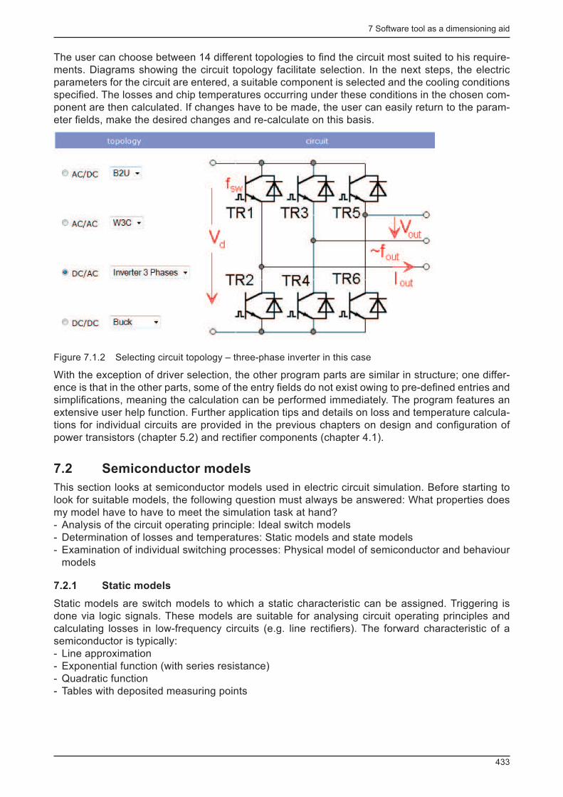
7 Software tool as a dimensioning aid
433
The user can choose between 14 different topologies to fi nd the circuit most suited to his require-ments. Diagrams showing the circuit topology facilitate selection. In the next steps, the electric parameters for the circuit are entered, a suitable component is selected and the cooling conditions specifi ed. The losses and chip temperatures occurring under these conditions in the chosen com-ponent are then calculated. If changes have to be made, the user can easily return to the param-eter fi elds, make the desired changes and re-calculate on this basis.
Figure 7.1.2 Selecting circuit topology – three-phase inverter in this case
With the exception of driver selection, the other program parts are similar in structure; one differ-ence is that in the other parts, some of the entry fi elds do not exist owing to pre-defi ned entries and simplifi cations, meaning the calculation can be performed immediately. The program features an extensive user help function. Further application tips and details on loss and temperature calcula-tions for individual circuits are provided in the previous chapters on design and confi guration of power transistors (chapter 5.2) and rectifi er components (chapter 4.1).
7.2 Semiconductor models
This section looks at semiconductor models used in electric circuit simulation. Before starting to look for suitable models, the following question must always be answered: What properties does my model have to have to meet the simulation task at hand? - Analysis of the circuit operating principle: Ideal switch models - Determination of losses and temperatures: Static models and state models - Examination of individual switching processes: Physical model of semiconductor and behaviour models
7.2.1 Static models
Static models are switch models to which a static characteristic can be assigned. Triggering is done via logic signals. These models are suitable for analysing circuit operating principles and calculating losses in low-frequency circuits (e.g. line rectifi ers). The forward characteristic of a semiconductor is typically: - Line approximation - Exponential function (with series resistance) - Quadratic function - Tables with deposited measuring points
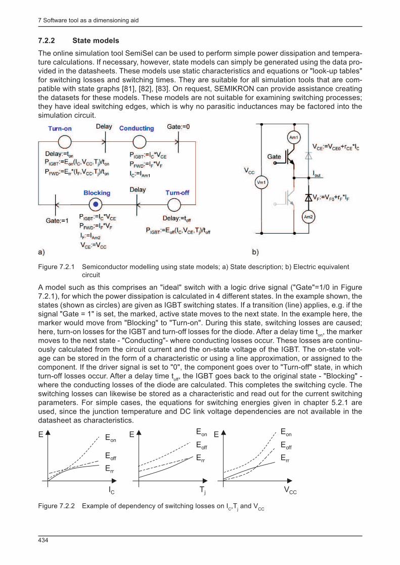
7 Software tool as a dimensioning aid
434
7.2.2 State models
The online simulation tool SemiSel can be used to perform simple power dissipation and tempera-ture calculations. If necessary, however, state models can simply be generated using the data pro-vided in the datasheets. These models use static characteristics and equations or "look-up tables" for switching losses and switching times. They are suitable for all simulation tools that are com-patible with state graphs [81], [82], [83]. On request, SEMIKRON can provide assistance creating the datasets for these models. These models are not suitable for examining switching processes; they have ideal switching edges, which is why no parasitic inductances may be factored into the simulation circuit.
Figure 7.2.1 Semiconductor modelling using state models; a) State description; b) Electric equivalent circuit
A model such as this comprises an "ideal" switch with a logic drive signal ("Gate"=1/0 in Figure 7.2.1), for which the power dissipation is calculated in 4 different states. In the example shown, the states (shown as circles) are given as IGBT switching states. If a transition (line) applies, e.g. if the signal "Gate = 1" is set, the marked, active state moves to the next state. In the example here, the marker would move from "Blocking" to "Turn-on". During this state, switching losses are caused; here, turn-on losses for the IGBT and turn-off losses for the diode. After a delay time t
on , the marker
moves to the next state - "Conducting"- where conducting losses occur. These losses are continu-ously calculated from the circuit current and the on-state voltage of the IGBT. The on-state volt-age can be stored in the form of a characteristic or using a line approximation, or assigned to the component. If the driver signal is set to "0", the component goes over to "Turn-off" state, in which turn-off losses occur. After a delay time t
off , the IGBT goes back to the original state - "Blocking" -
where the conducting losses of the diode are calculated. This completes the switching cycle. The switching losses can likewise be stored as a characteristic and read out for the current switching parameters. For simple cases, the equations for switching energies given in chapter 5.2.1 are used, since the junction temperature and DC link voltage dependencies are not available in the datasheet as characteristics.
IC
E Eon
Eoff
Err
Tj
E Eon
Eoff
Err
VCC
E Eon
Eoff
Err
Figure 7.2.2 Example of dependency of switching losses on I C ,T
j and V
CC
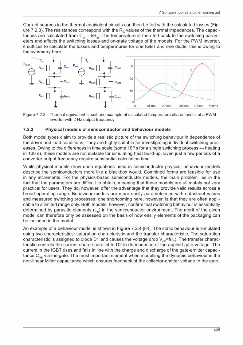
7 Software tool as a dimensioning aid
435
Current sources in the thermal equivalent circuits can then be fed with the calculated losses (Fig-ure 7.2.3). The resistances correspond with the R
th values of the thermal impedances. The capaci-
tances are calculated from C th = t/R
th . The temperature is then fed back to the switching param-
eters and affects the switching losses and on-state voltage of the models. For the PWM inverter, it suffi ces to calculate the losses and temperatures for one IGBT and one diode; this is owing to the symmetry here.
PIGBT
TjI
0
10
20
30
0 500ms200ms 400ms
TjI
TjD
100ms 300ms
RthD3 CthD3
PFWD
TjD
RthD2
RthD1
CthD2
CthD1
CthI3
CthI2
CthI1
RthI3
RthI2
RthI1
Figure 7.2.3 Thermal equivalent circuit and example of calculated temperature characteristic of a PWM inverter with 2 Hz output frequency
7.2.3 Physical models of semiconductor and behaviour models
Both model types claim to provide a realistic picture of the switching behaviour in dependence of the driver and load conditions. They are highly suitable for investigating individual switching proc-esses. Owing to the differences in time scale (some 10 -9 s for a single switching process ↔ heating in 100 s), these models are not suitable for simulating heat build-up. Even just a few periods of a converter output frequency require substantial calculation time.
While physical models draw upon equations used in semiconductor physics, behaviour models describe the semiconductors more like a blackbox would. Combined forms are feasible for use in any increments. For the physics-based semiconductor models, the main problem lies in the fact that the parameters are diffi cult to obtain, meaning that these models are ultimately not very practical for users. They do, however, offer the advantage that they provide valid results across a broad operating range. Behaviour models are more easily parameterised with datasheet values and measured switching processes; one shortcoming here, however, is that they are often appli-cable to a limited range only. Both models, however, confi rm that switching behaviour is essentially determined by parasitic elements (L
S ) in the semiconductor environment. The merit of the given
model can therefore only be assessed on the basis of how easily elements of the packaging can be included in the model.
An example of a behaviour model is shown in Figure 7.2.4 [84]. The static behaviour is simulated using two characteristics: saturation characteristic and the transfer characteristic. The saturation characteristic is assigned to diode D1 and causes the voltage drop V
CE =f(I
C ). The transfer charac-
teristic controls the current source parallel to D2 in dependence of the applied gate voltage. The current in the IGBT rises and falls in line with the charge and discharge of the gate-emitter capaci-tance C
GE via the gate. The most important element when modelling the dynamic behaviour is the
non-linear Miller capacitance which ensures feedback of the collector-emitter voltage to the gate.
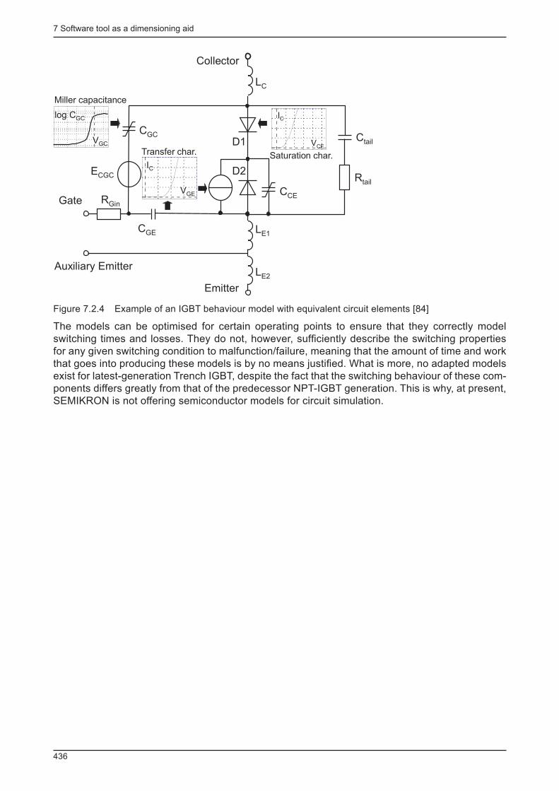
7 Software tool as a dimensioning aid
436
LC
CGC
CGE
CCE
Ctail
Rtail
ECGC
LE1
LE2
RGin
log CGC
VGC
Miller capacitance
IC
VCE
Saturation char.
VGE
IC
Transfer char.
Auxiliary Emitter
D2
D1
Gate
Emitter
Collector
Figure 7.2.4 Example of an IGBT behaviour model with equivalent circuit elements [84]
The models can be optimised for certain operating points to ensure that they correctly model switching times and losses. They do not, however, suffi ciently describe the switching properties for any given switching condition to malfunction/failure, meaning that the amount of time and work that goes into producing these models is by no means justifi ed. What is more, no adapted models exist for latest-generation Trench IGBT, despite the fact that the switching behaviour of these com-ponents differs greatly from that of the predecessor NPT-IGBT generation. This is why, at present, SEMIKRON is not offering semiconductor models for circuit simulation.
References
437
References
[AN1] AN-7006: IGBT Peak Voltage Measurement and Snubber Capacitor Specifi cation; www.semikron.com
[AN2] AN-8003: SEMIKUBE B6CI USER MANUAL, SEMIKUBE selection guide; www.semikron.com
[AN3] AN-7002: Connection of Gate Drivers; www.semikron.com
[AN4] AN-9001: IGBT4 and free wheeling diode CAL4 in IGBT modules; www.semikron.com
[AN5] AN-7003: Gate Resistor; www.semikron.com
[AN6] AN-7004: IGBT Driver Calculation; www.semikron.com
[1] Backlund, B.; Rahimo, M.: "High Voltage Bipolar Semiconductor Technologies", Bodo’s Power Systems, 12/2009, pp. 34-36
[2] Kaminski, N.: "State of the Art and the Future of Wide Band-Gap Devices", EPE 2009, Conference Proceedings
[3] Majumdar, G.; Oomori, T.: "Some key researches on SiC device technologies and their predicted advantages", EPE 2009, Conference Proceedings
[4] Silber, D.; Novak, W.-D.; Wondrak, W.; Thomas, B.; Berg, H.: "Improved Dynamic Pro-perties of GTO-Thyristors and Diodes by Proton Implantation", Electron Device Meeting, 1985
[5] Lutz, J.; Scheuermann, U.: "Advantages of the New Controlled Axial Lifetime Diode", PCIM Europe 1994, Conference Proceedings
[6] Lutz, J.: "Axial Recombination Center Technology for Freewheeling Diodes", EPE 1997, Conference Proceedings
[7] Lutz, J.: "The Freewheeling Diode - No Longer the Weak Component", PCIM Europe 1997, Conference Proceedings
[8] Weber, A.; Galsterer, N.; Tsyplakow, E.: "A New Generation of Asymmetric and Reverse Conducting GTOs and Their Snubber Diodes", PCIM Europe 1997, Conference Procee-dings
[9] Baliga, B.J.: "Analysis of a High Voltage Merged p-i-n/Schottky (MPS) Rectifi er", IEEE El. Dev. Letters Vol. Edl.-8, No.9 (1987)
[10] Sze, S.M.: "Physics of Semiconductor Devices", John Wiley & Sons, Inc., New York, 2006, ISBN 978-0471143239
[11] Dannhäuser, F.; Krausse, J.: "Die Abhängigkeit der Trägerbeweglichkeit in Silizium von der Konzentration der freien Ladungsträger", Solid State Electronics Vol. 15, pp. 1371-1381, (1972)
[12] Baliga, B.J.: "Modern Power Devices", John Wiley & Sons, Inc., New York, 1987
[13] Wolley, E.D.; Bevaqua, S.F.: "High speed, soft recovery epitaxial diodes for power inverter circuits", IEEE IAS Meeting Digest; 1981
[14] Silber, D.: "Leistungsbauelemente: Funktionsprinzipien und Entwicklungstendenzen", ETG-Fachtagung "Bauelemente der Leistungselektronik und ihre Anwendungen", Bad Nauheim 1998, Proceedings, pp. 9-25
[15] Satoh,K.; Takahashi, T.; Fujii, H.; Yoshino, M.; Donlon, J.F.: "New chip design technology for next generation power module", PCIM Europe 2007, Conference Proceedings
[16] Bayerer, R.: "Higher Junction Temperature in Power Modules – a demand from hybrid cars, a potential for the next step increase in power density for various Variable Speed Drives", PCIM Europe 2008, Conference Proceedings
References
438
[17] Lutz, J.: "Halbleiter-Leistungsbaulemente: Physik, Eigenschaften, Zuverlässigkeit", Springer Verlag Berlin Heidelberg 2006, ISBN 3-540-34206-0
[18] Rusche, W.: "Die vierte IGBT-Generation. Moderne IGBT ermöglichen Energieeinsparun-gen bei industriellen Anwendungen", www.elektroniknet.de
[19] Dewar, S.; Linder, S.; von Arx, C.; Mukhitinov, A.; Debled, G.: "Soft Punch Through (SPT) – Setting new Standards in 1200 V IGBT", PCIM Europe 2006, Conference Proceedings
[20] Cammarata, M.; Kopta, A.; Rahimo, M.; Klaka, S.; Richter, F.; Geissman, S.: "1200 V SPT+ IGBT and Diode Chip-Set for High DC-link Voltage Applications", PCIM Europe 2009, Conference Proceedings
[21] IGBT Modules Application Note: "The 5th Generation IGBT Chip", Mitsubishi 12/2007
[22] Takeda, T.; Kuwahara, M.; Kamata, S.; Tsunoda, T.; Imamura, K.; Nakao, S.: "1200 V trench gate NPT-IGBT (IEGT) with excellent low on-state voltage", ISPSD 1998, Confer-ence Proceedings
[23] Eckel, H.-G.: "Potential of Reverse Conducting IGBT in Voltage Source Inverters", PCIM Europe 2009, Conference Proceedings
[24] Buonomo, S.; Crisafulli, V.; Vitale, G.; Nania, M.; Scollo, R.: "ESBT® Technology in In-dustrial Converters: The Best Way to Cut Your Losses", PCIM Europe 2008, Conference Proceedings
[25] Kapels, H.; Schmitt, M.; Kirchner, U.; Aloise, G.; Bjoerk, F.: "New 900 V Voltage Class for Junction Devices – A New Horizon for SMPS and Renewable Energy Applications", PCIM Europe 2008, Conference Proceedings
[26] Stengl, J.P.; Tihanyi, J.: "Leistungs-MOSFET-Praxis", Pfl aum Verlag Munich, 2nd edition, 1992
[27] Gillberg, J.: "Mixed Signal and Power Integration Packaging Solutions", Bodo's Power Systems, 10/2009, pp. 32-34
[28] Lutz, J.; Reimann, T.: "Advanced Design with MOSFET and IGBT Power Modules", Tuto-rial, PCIM Europe 2007, Conference Proceedings
[29] Siemieniec, R.; Hirler, F.; Geissler, D.: "Space-saving edge-termination structures for verti-cal charge compensation devices", EPE 2009, Conference Proceedings
[30] Eisele, R.; Rudzki, J.; Kock, M.: "Pressure Sintering for Thermal Stack Assembly", PCIM Europe 2007, Conference Proceedings
[31] Rudzki, J.: "Aufbaukonzepte für die Leistungselektronik mit der Niedertemperatur-Verbind-ungstechnik", diss., VDI Verlag, Düsseldorf, 2006, ISBN 3-18-337621-0
[32] Eisele, Migdalek, Rabsch, Rudzki: "Reliable Chip Contact Joining", PCIM Europe 2009, Conference Proceedings
[33] Sleven, M.; Luniewski, P.: "Wind Turbine Inverter Technology – the Quest for Increased Reliability", Power Systems Design Europe, 09/2009
[34] Chandler, G.; Zimmer, J.: "SOD Substrates: The next Step in Electronics Thermal Man-agement", Workshop on thermal management, Palo Alto USA, 09/2006
[35] Mitsubishi IGBT manual 2009, http://www.mitsubishichips.com/Global/fi les/manuals/igbt_note_e.pdf
[36] Maruta, A.; Tabata, M.: "2500 A / 1200 V Dual IGBT Module", PCIM Europe 2009, Confer-ence Proceedings
[37] Konrad, S.: "Ein Beitrag zur Auslegung und Integration spannungsgespeister IGBT-Wech-selrichter", diss. TU Ilmenau 1997, ISLE Verlag, ISBN 3-932633-09-1
References
439
[38] Klotz, F.: "Leitungsgebundene elektrische Störemissionen von Leistungshalbleitertopolo-gien", diss. TU Ilmenau 1997; ISLE Verlag, ISBN 3-932633-00-8
[39] Zeller, H.: "High Power Components", PCIM Europe 1998, Conference Proceedings
[40] Setz, T.; Lüscher, M.: Application note "Applying IGCT”, www.abb.com/semiconductors
[41] Mitsubishi Datasheet MG400V1US51A, http://www.mitsubishichips.com/Global/
[42] Wolfgang, E.: ECPE Workshop "Semiconductor Robustness - What Kills Power Devices", Munich, 06/2009
[43] ZVEI, Handbook for Robustness Validation of Semiconductor Devices in Automotive Ap-plications, http://www.zvei.org/
[44] Lang, F.; Scheuermann, U.: "Reliability of spring pressure contacts under environmental stress”, European Symposium on Reliability of Electronic Devices, Failure Physics and Analysis 2007, Proceedings Microelectronics Reliability
[45] Slade, P. G.: "Electrical Contacts: Principles and Application", Marcel Dekker Inc. 1999, pp. 343-345
[46] Lang, F.; Scheuermann, U.: "Spring Pressure Contacts for Flexible Reliable Interconnec-tions in Power Modules", PCIM China 2009, Conference Proceedings
[47] Lutz, J. et al.: "Power cycling induced failure mechanisms in the viewpoint of rough tem-perature environment", CIPS 2008, Conference Proceedings
[48] Amro; Lutz; Lindemann: "Power Cycling with High Temperature Swing of Discrete Compo-nents based on Different Technologies", Power Electronics Specialists Conference 2004 (PESC04), Aachen, Conference Proceedings
[49] Ramminger, S.; Seliger, N.; Wachutka, G.: "Reliability Model for Al Wire Bonds Subjected to Heel Crack Failures", Microelectronics Reliability 40 (2000)
[50] Eicher, S.; Rahimo, M.; Tsyplakov, E.; Schneider, D.; Kopta, A.; Schlapbach, U.; Carroll, E.: "4.5 kV Press Pack IGBT Designed for Ruggedness and Reliability", IAS Annual Meet-ing 2004, Seattle, Conference Proceedings
[51] Hamidi, A.; Kaufmann, S.; Herr, E.: "Increased Lifetime of Wire Bond Connections for IGBT Power Modules", IEEE Applied Power Electronic Conference and Exhibition (APEC), Ana-heim, 2001, Conference Proceedings
[52] Held, M.; Jacob, P.; Nicoletti, G.; Scacco, P.; Poech, M.H.: "Fast Power Cycling Test for IGBT Modules in Traction Application", Power Electronics and Drive Systems 1997, Con-ference Proceedings
[53] Bayerer, R.; Herrmann, T.; Licht, T.; Lutz, J.; Feller, M.: "Model for Power Cycling Lifetime of IGBT Modules – Various Factors Infl uencing Lifetime", CIPS 2008, Conference Pro-ceedings
[54] Pfeiffer, W. (ed.): "Isolationskoordination in Niederspannungsanlagen", VDE 0110, expert-Verlag Böblingen, 1990
[55] Srajber, D. Lukasch, W.: "The calculation of the power dissipation for the IGBT and the inverse diode in circuits with sinusoidal output voltage", electronica‘92, Conference Pro-ceedings
[56] "Simulation tool R-theta", www.r-theta.com
[57] Seri Lee: Electronics Cooling Magazine, Aavid Thermal Technologies
[58] Lytron: "Die besten Wärmeübertragungsfl üssigkeiten für Flüssigkeitskühlung", http://www.lytron.de/tools-technical/notes/
[59] Eisele, R.; Olesen, K.K.; Osterwald, F.: "ShowerPower — Brausestrahl versus traditionelle Flüssigkeitskühlung", Elektronik Praxis 10/2008

References
440
[60] Zverev, I.: "Untersuchungen energiearmer Prozesse in Stromrichtern", diss., University of Rostock, 1999, ISLE Verlag, Ilmenau, 1999, ISBN 3-932633-39-3
[61] Scheuermann, U.: "Paralleling of Chips – From the Classical ‘Worst Case’ Consideration to a Statistical Approach", PCIM Europe 2005, Conference Proceedings
[62] Wintrich, A.; Nascimento, J.; Leipenat, M.: "Infl uence of parameter distribution and me-chanical construction on switching behaviour of parallel IGBT", PCIM Europe 2006, Con-ference Proceedings
[63] Bruckmann, M.; Sigg, J.; Türkes, P.: "Reihenschaltung von IGBT’s in Experiment und Simulation", 24. Colloquium "Halbleiter-Leistungsbauelemente und Materialgüte von Sil-izium", Freiburg, 1995, Conference Proceedings, Paper no. 6
[64] Bruckmann, M.: "Einsatz von IGBT für Hochleistungsstromrichter",ETG-Fachtagung "Bauelemente der Leistungselektronik und ihre Anwendungen", Bad Nauheim, 1998, Proc. pp. 221-234
[65] Gerster, Ch.; Hofer, P.; Karrer, N.: "Gate-control Strategies for Snubberless Operation of Series Connected IGBTs”, PESC’96, Baveno, Proc. Vol. II, pp. 1739-1742
[66] Ruedi, H.; Köhli, P.; u.a.: "Dynamic Gate Controller (DGC) – A New IGBT Gate Unit for High Current / High Voltage IGBT Modules", PCIM Europe 1995, Conference Proceedings
[67] Helsper; Fuchs: "Adaptation of IGBT Switching Behaviour by Means of Active Gate Drive Control for Low and Medium Power", EPE 2003, Conference Proceedings
[68] Palmer, P.R.; Githiari, A.N.: "The Series Connection of IGBTs with Optimized Voltage Shar-ing in the Switching Transient", PESC 1995, Atlanta, USA, Proc. Vol. I, pp. 44-49
[69] Reimann, T.; Krümmer, R.; Petzoldt, J.: "Active Voltage Clamping Techniques for Overvolt-age Protection of MOS-Controlled Power Transistors", EPE 1997, Conference Proceed-ings
[70] Reimann, T.; Krümmer, R.; Petzoldt, J.: "Experimental and Simulative Investigations of Power Losses in Active Voltage Clamping Circuits", PEMC’98, Prague, Vol. 1, pp. 1-1 – 1-6
[71] Eckel, H.G.: "Series Connection of IGBTs in Zero Voltage Switching Inverters"PCIM Europe 1997, Conference Proceedings
[72] Teigelkötter, J.: "Schaltverhalten und Schutzbeschaltungen von Hochleistungshalbleitern", diss., Ruhr-Universität Bochum, 1996, VDI-Verlag, 1996, ISBN 3-18-320621-8
[73] Krümmer, R.: "Beitrag zur Verbesserung der elektrischen und thermischen Ausnutzung von Leistungshalbleiterschaltern", diss., TU Ilmenau, 2005, ISLE Verlag, Ilmenau, 2005, ISBN 3-938843-04-7
[74] Helsper, M.: "Analyse und Verbesserung des Verhaltens von Planar- und Trench-IGBT-Modulen in hart bzw. weich schaltenden Applikationen", diss., Christian-Albrechts-Univer-sität Kiel, 2003, Shaker Verlag, Aachen, 2004, ISBN 3-8322-2621-4
[75] Dörlemann, Ch.: "Geregelte Ansteuerung von Insulated Gate Bipolar Transis-toren (IGBT)", diss., Ruhr-Universität Bochum, 2002, Shaker Verlag, Aachen, 2002, ISBN 3-8322-0701-5
[76] Reimann, T.: "Verhalten abschaltbarer Leistungshalbleiterbauelemente im ZVS-Mode", diss., TU Ilmenau, 1994, Verlag Shaker, Aachen, 1995, ISBN 3-8265-0538-7
[77] Bernet, S.: "Leistungshalbleiter als Nullstromschalter in Stromrichtern mit weichen Schaltvorgängen", diss., TU Ilmenau, 1995, Verlag Shaker, Aachen, 1995, ISBN 3-8265-0762-2
[78] Dehmlow, M.: "Vergleichende Betrachtung unterschiedlicher resonanter Umrichtertopolo-gien", diss., TU Berlin, 1995

References
441
[79] Hoffmann, K.F.; Kärst, J.P.; Rexhausen, W.: "Reduced IGBT Conducting Power Losses by Miller Effect Triggered Gate Current Injection”, PCIM Europe 2006, Conference Procee-dings
[80] "Failure Rates of HiPak Modules Due to Cosmic Rays", Application Note 5SYA 2042-03. Nando Kaminski, Arnost Kopta ABB Switzerland Ltd, Semiconductors, July 2009
[81] PORTUNUS® www.adapted-solutions.com
[82] SIMPLORER® www.ansoft.com
[83] PLECS® www.plexim.com
[84] Wintrich, A.: "Verhaltensmodellierung von Leistungshalbleitern für den rechnergestützten Entwurf leistungselektronischer Schaltungen", diss., TU Chemnitz, 1996; http://archiv.tu-chemnitz.de/pub/1998/0023/data/inhalt.htm

Abbreviations used in SEMIKRON Datasheets
442
Abbreviations used in SEMIKRON Datasheets
Acronym English German
(di/dt) cr
Critical rate of rise of on-state current
Kritische Stromsteilheit
(dv/dt) cr
Critical rate of rise of off-state voltage
Kritische Spannungssteilheit
∫ vdt Voltage-time integral at no load Spannungs-Zeit-Fläche bei Leerlauf
a Maximum acceleration under vibration
Zulässige Beschleunigung beim Schalten
b Width of the module base Breite des Modulbodens
B2 Two-pulse bridge connection Zweipuls-Brückenschaltung
B25/85 Exponent of temperature sen-sor equation
Exponent für Temperatursen-sor Gleichung
B6 Six-pulse bridge connection Sechspuls-Brückenschaltung
BW Ioutsens
Bandwith of output current sensing
Bandbreite der Strommessung
BW TBsens
Bandwith of temperatur sens-ing on driver board
Bandbreite der Temperatur-Messelektronik
BW TCSsens
Bandwith of temperatur sens-ing on ceramic-substrate
Bandbreite des Temper-atursensors
BW VDCsens
Bandwith of DC-link-voltage sensing
Bandbreite der Zwischenkre-isspannungserfassung
C CHC
Capacitance chip-case (base-plate)
Kapazität Chip-Gehäuse (Grundplatte)
C DC
Capacitance of DC-link capaci-tor bank
Kapazität des Zwischenkre-iskondensators
C eqvl
Equivalent capacitance of a DC-link capacitor bank
Ersatzkapazität einer Zwischenkreiskondensator-bank
C ies
Input capacitance, output short-circuited (IGBT)
Eingangskapazität, Ausgang kurzgeschlossen (IGBT)
C IN
Input capacitance Input capacitance
C iss
Input capacitance, output short-circuited (MOS)
Eingangskapazität, Ausgang kurzgeschlossen (MOSFET)
C j
Junction capacitance Sperrschichtkapazität
C L
Load capacitor Lastkondensator
C max
Maximum value of reservoir capacitor
Größter Ladekondensator (bei größerem C Strom verringern)
C oes
Output capacitance, input short-circuited (IGBT)
Ausgangskapazität, Eingang kurzgeschlossen (IGBT)
C oss
Output capacitance, input short-circuited (MOSFET)
Ausgangskapazität, Eingang kurzgeschlossen (MOSFET)

Abbreviations used in SEMIKRON Datasheets
443
C ps
Coupling capacitance, primary to secondary winding
Koppelkapazität zwischen Primär- und Sekundärwicklung
C res
Reverse transfer capacitance (Miller capacitance) (IGBT)
Rückwirkkapazität (Miller-Ka-pazität) (IGBT)
C rss
Reverse transfer capacitance (Miller capacitance) (MOSFET)
Rückwirkkapazität (Miller-Ka-pazität) (MOSFET)
D Duty cycle. D =f · tp Tastverhältnis D=f · tp
di/dt change of current per time Stromänderung pro Zeiteinheit
di D /dt
Rate of fall ot the drain current (MOSFET)
Abklingsteilheit des Drain-stroms (MOSFET)
di F /dt
Rate of rise of the forward cur-rent (Diode)
Anstiegssteilheit des Durch-lassstromes (Diode)
di F /dt
Rate of fall of the forward cur-rent (Diode)
Abklingsteilheit des Durch-lassstromes (Diode)
di G /dt Rate of rise of gate current
Anstiegssteilheit des Durch-lassstromes (Thyr.)
di T /dt Rate of rise of Thyristor current
Anstiegssteilheit des Steuer-stroms
di T /dt Rate of fall of Thyristor current
Abklingsteilheit des Durch-lassstromes (Thyr.)
DSC Double sided cooling Beidseitige Kühlung
d tp
thickness of thermal paste Dicke der Wärmeleitpaste
dv/dt change of voltage per time Spannungsänderung pro Zeiteinheit
dV/dt Volume fl ow Volumenstrom
E cond
Energy dissipation during con-duction time
Verlustenergie während der Stromfl usszeit
ED Intermittend duty Relative Einschaltdauer (Aus-setzbetrieb) = te/tsp
E off
Energy dissipation during turn-off
Verlustenergie während der Abschaltzeit
E on
Energy dissipation during turn-on
Verlustenergie während der Einschaltzeit
E P
Maximum permissible non-repetitive peak pulse energy (rectangular pulse 2 ms)
Höchstzulässiger nichtperio-discher Impulsenergie Spitzen-wert (Rechteckpuls 2 ms)
E rr
Energy dissipation during re-verse recovery (diode)
Verlustenergie während der Sperrverzögerungszeit
E RSM
Non repetitive peak reverse avalanche energy
Einmalig zulässige Avalanche Energie
E tp
dielectric strength of thermal paste
Durchschlagsfestigkeit der Wärmeleitpaste
f Operating frequency Betriebsfrequenz
F Mounting force Montagekraft
f Fan
AC voltage frequency for fan operation
Frequenz der Lüfterspannung
f max
Maximum frequency Maximale Frequenz

Abbreviations used in SEMIKRON Datasheets
444
f out
Output requency of a circuit Ausgangsfrequenz einer Schaltung
f sw
Switching frequency Puls-, Schaltfrequenz
Fu Recommended fuse (fast act-ing)
Empfohlene Sicherung (fl ink bzw. überfl ink)
g fs
Forward transconductance Übertragungssteilheit
g tp (γ)
specifi c gravity of thermal paste
Spezifi sches Gewicht der Wärmeleitpaste
HIN PWM signal input high side switch
Eingang PWM Signal TOP Schalter
I Length of the heatsink profi le Länge des Kühlprofi ls
i 2 t i2t value Grenzlastintegral
I AC-terminal
AC-Terminal current Wechselstrom-Anschluss Strom
I analogOUT
Current sensor refference value (SKiiP)
Nennstrom der Stromsensor-auswertung (SKiiP)
I C
Continuous collector current Kollektor-Gleichstrom
I CES
Collector-emitter cut-off cur-rent with gate-emitter short-circuited
Kollektor-Emitter-Leckstrom, Gate-Emitter kurzgeschlossen
I Cnom
Nominal collector current Kollektor Nennstrom
I CRM
Repetitive peak collector cur-rent
Periodischer Kollektor Spitzen-strom
I CSM
Non-repetitive peak collector current
Nichtperiodischer Kollektor-Spitzenstrom
I D
Direct output current (of a recti-fi er connection)
Ausgangsgleichstrom (einer Gleichrichterschaltung)
I D
Continuous drain current (MOSFET)
Drain-Dauergleichstrom (MOSFET)
I D(CL)
Direct output current with ca-pacitive load (limiting value)
Ausgangsgleichstrom bei C-Last (Grenzwert)
I DD
Forward off-state current (Thy-ristor)
Gleichsperrstrom (in Vorwärt-srichtung)
I DM
Peak value drain current Spitzenwert Drainstrom
I DR
Continuous reverse drain cur-rent (inverse diode forward current)
Drain-Gleichstrom in Rückwärt-srichtung (Durchlassstrom der Inversdiode)
I DRM
Peak value of reverse drain current, (inverse diode forward current)
Spitzenwert des Drainstroms in Rückwärtsrichtung (Durch-lassstrom der Inversdiode)
I DSS
Drain-Source cut-off current with gate source short-circuited
Drain-Source-Leckstrom, Gate-Source kurzgeschlossen
I E
Continuous emitter current Emitter-Gleichstrom
i F
Forward current (actual value) Durchlassstrom (Augenblick-swert)
I F(CL)
Mean forward current with capacitive load
Dauergrenzstrom bei kapazi-tiver Last

Abbreviations used in SEMIKRON Datasheets
445
I F(OV)
Overload forward current Überlast-Durchlassstrom
I Fan
Current for fan operation Lüfterstrom
I FAV
Mean forward current Mean forward current
I FM
Peak forward current Durchlassstrom-Spitzenwert
I FN
Recommended mean forward current
Empfohlener Durchlassstrom-Mittelwert
I FRM
Repetitive peak forward current Periodischer Spitzenstrom
I FRMS
RMS forward current Durchlassstrom-Effektivwert
I FSM
Surge forward current Stoßstrom-Grenzwert
I G
Gate current Gatestrom
I GD
Gate non-trigger current höchster nichtzündender Gat-estrom
I GES
Gate-emitter leakage current, collector emitter short-circuited
Gate-Emitter-Leckstrom, Kolle-ktor-Emitter kurzgeschlossen
I Goff
max. turn-off output current (driver)
Max. Ausgangs-Abschalt-spitzenstrom (Treiber)
I Gon
max. turn-on output current (driver)
Max. Ausgangs-Einschalt-spitzenstrom (Treiber)
I GSS
Gate-source leakage current, drain-source short-circuited
Gate-Source-Leckstrom, Kolle-ktor-Emittler kurzgeschlossen
I GT
Minimum guaranteed gate trig-ger current
Mindestzündstrom für sicheres Einschalten
I H
Hold current Haltestrom
I iH
Input signal current (High) Eingangssignalstrom (High)
I L
Latching current Einraststrom
I M
Highest peak current obtain-able at a rise time lower than 1 ųs (pulse transformers)
Höchster bei einer Anstiegszeit unter 1µs erreichbarer Spitzen-strom (Impulsübertrager)
I max(EO)
Maximum Error Output Current Maximaler Strom des Fehler-ausgangs
I N
Nominal current Empfohlener Gleichstrom
I N(CL)
Recommended direct output current with capacitive load
Empfohlener Gleichstrom bei C-Last
I nom
Nominal current Nennstrom
I Omax
Max. output current (driver) Max. Ausgangsstrom (Treiber)
I out
Output current of a circuit Ausgangsstrom einer Schaltung
I outAV
Output average current (driver) Ausgangsstrommittelwert (Treiber)
I outPEAK
Output peak current (driver) Ausgangsstromspitzenwert (Treiber)
I outsens
AC sensing range Wechselstrom Messbereich
I outtrip
AC over current trip level Überstrom-Fehler Grenzwert

Abbreviations used in SEMIKRON Datasheets
446
I overload
Overload current for a speci-fi ed time
Überlaststrom für eine bestim-mte Zeit
I peak(1)
magnitude of the fi rst hamonic of a current
Amplitude der ersten Harmo-nischen eines Stromes
I R
Reverse current Off-state current
I RD
Direct reverse current (Thyris-tor)
Gleichsperrstrom in Rückwärt-srichtung (Thyristor)
I RMS
Maximum r.m.s current of a complete AC-controller circuit
Maximaler Effektivstrom eines Wechselspannungsstellers
I rr
Reverse recovery current (measuring condition for t
f and
t rr )
Sperrverzögerungsstrom (Messbedingung für t
f und t
rr )
I RRM
Peak reverse recovery current Rückstromspitze
I RSM
Maximum non-repetitive peak reverse current (avalanche diodes)
Höchstzulässiger nichtperio-discher Stoßspitzensperrstrom (Avalanche-Dioden)
I S
Supply current primary side Versorgungsstrom primärseitig (Treiber)
I S0
Supply current primary side (driver) at no load
Versorgungsstrom prim. Leer-lauf (Treiber)
i T
On-State current (instantane-ous value)
Durchlassstrom (Augenblick-swert)
I T
(Direct) on-state current Durchlass(gleich)strom
I T(OV)
Overload on-state current Durchlass-Überstrom
I TAV
Mean on-state current Mean forward current
I TM
Peak on-state current Durchlassstrom-Spitzenwert
ITRIP Comperator input for current measurement
Komperatorschwellwert für Strommess-Eingang
I TRIPLG
Ground fault current trip level (SKiiP)
Erdschlussfehler Stromgren-zwert (SKiiP)
I TRIPSC
Over current trip level (SKiiP) Überstrom-Fehler Grenzwert (SKiiP)
I TRMS
RMS on-state current Durchlassstrom-Effektivwert
I TSM
Surge on-state curren Stoßstrom-Grenzwert
I z
Tail current (IGBT) Schweifstrom (IGBT)
L inductance Induktivität
L CE
Parasitic collector-emitter inductance
Parasitäre Kollektor-Emitter-Induktivität
L DS
Parasitic drain-source induct-ance
Parasitäre Drain-Source-Induk-tivität
L ext
External circuit inductance (short circuit)
Externe Schaltungsinduktivität (im Kurzschluss)
LIN PWM singnal input low side switch
Eingang PWM Signal BOT-TOM Schalter
L p
Inductance of the primary winding at 1 kHz
Induktivität der Primärwicklung bei 1 kHz

Abbreviations used in SEMIKRON Datasheets
447
L s
Stray inductance Streuinduktivität
L ss
Parasitic stray inductance (Transformer secundary side)
Streuinduktivität (Sekundär-seite Übertrager)
l tp (λ)
thermal conductivity of thermal paste
Wärmeleitfähigkeit der Wärme-leitpaste
M Mounting torque Anzugsdrehmoment bei der Montage
M 1
Torque for mounting the semi-conductor to the heatsink
Anzugsdrehmoment für die Montage des Bauelements auf dem Kühlkörper
M 2
Torque for mounting the bus-bars to the semiconductor
Anzugsdrehmoment für die Montage der Stromschienen auf dem Bauelement
M ac
Mounting torque for AC termi-nals
Anzugsdrehmoment für AC - Anschluss
M dc
Mounting torque for DC termi-nals
Anzugsdrehmoment für DC - Anschluss
M s
Mounting torque on heat sink Anzugsdrehmoment für Mon-tage auf Kühlkörper
M t
Mounting torque for terminals Anzugsdrehmoment für An-schlüsse
n specifi ed number Anzahl von…
N Maximum number of serie con-nected silicon elements
Höchstzahl der Siliziumele-mente in Reihenschaltung
N p /N
s
Ratio of winding primary to secondary
Übersetzungsverhältnis Wind-ungszahl prim/sec.
Ø d Contact diameter of capsule devices
Kontaktdurchmesser bei Scheibenzellen
P AV
Maximum permissible average power dissipation
Hochzulässige Dauerver-lustleistung Mittelwert
p coolant
pressure of coolant Druckabfall Kühlfl üssigkeit
P D
Power dissipation of one com-ponent
Verlustleistung eines Bauele-ments
P Fan
Power consumption of fan Leistungsaufnahme des Lüfters
P FAV
Mean forward power dissipa-tion
Mittlere Durchlassverlustleis-tung
P FM
Peak forward power dissipation Spitzenwert der Durchlassver-lustleistung
P G
Peak gate power dissipation Spitzenwert der Steuerver-lustleistung
P R
Reverse power dissipation Sperrverlustleistung
P RAV
Mean reverse power dissipa-tion
Mittlere Sperrverlustleistung
P RRM
Peak repetitive reverse power dissipatiom
Periodischer Spitzen-Sperrver-lustleistung
P RSM
Non-repetitive peak reverse power dissipation
Stoßspitzen-Sperrverlustleis-tung

Abbreviations used in SEMIKRON Datasheets
448
P TAV
Mean on-state power dissipa-tion (Thyristor)
Mittlere Durchlass-Verlustleis-tung (Thyristor)
P tot
Total power dissipation Gesamt-Verlustleistung
P W
Water pressure Wasserdruck
P ZSM
Non repetitive peak power dis-sipation (Zener diodes)
Stoßspitzen-Verlustleistung (Zener Dioden)
Q f
Charge recovered during the reverse current fall time
Ladung, die während der Rückstrom-Fallzeit abfl ießt
Q G
Gate charge (IGBT; MOSFET) Gate-Ladung (IGBT; MOSFET)
Qout/pulse Output charge per pulse (Driver)
Ausgangsladung pro pulse (Treiber)
Q rr
Reverse recovery charge Sperrverzögerungsladung
R CC'+EE'
Resistance of the interconnec-tions between terminals and die
Kompletter Anschlusswider-stand Terminal-Chip-Terminal
r CE
On-State slope resistance (IGBT)
Bahnwiderstand IGBT
R CE
Resistor for V CE
monitoring Widerstand für V
CE -Überwac-
hung (Treiber)
r DS(on)
Drain-source on-resistance (MOSFET)
Drain-Source-Einschaltwider-stand (On-Widerstand) MOS-FET
rec. Rectangular current waveform Rechteckförmiger Stromverlauf
rec. 120 Rectangular current pulse, 120° conduction angle
Rechteck-Strompuls, 120° Stromfl usswinkel
R EX
Auxiliary emitter series resistor (parallel IGBT)
Widerstand vor Hilfsemitter (für parallelgeschaltete IGBT)
r F
On-state slope resistance, for-ward slope resistance (Diode)
Durchlass- Ersatzwiderstand (Diode)
R G
Gate circuit resistance Externer Gate Widerstand
R Gint
Internal gate resistance Interner Gate Widerstand
R Goff
External gate series resistor at switch-off (MOSFET, IGBT)
Gatevorwiderstand zum Ab-schalten
R Goffmin
Minimum value of an external switch-off gate resistor (Driver)
Minimalwert für einen Externen Ausschalt-Gatewiderstand
R gon
External gate series resistor at switch-on (MOSFET, IGBT)
Gatevorwiderstand zum Ein-schalten
R Gonmin
Minimum value of an external switch-on gate resistor (Driver)
Minimalwert für einen Externen Einschalt-Gatewiderstand
R GS
Gate-source resistance (MOSFET)
Gate-Source-Widerstand (MOSFET)
RH storage
storage humidity Luftfeuchte bei Lagerung
R IN
Input resistance Eingangswiderstand
R iso
Insulation resistance Isolationswiderstand
R L
Load resistance Lastwiderstand

Abbreviations used in SEMIKRON Datasheets
449
R min(CL)
Minimum series resistor für capacitive load
Minimaler Schutzwiderstand bei C-Last
R P
Recommended parallel resis-tor for a series connection of demiconductors
Empfohlener Parallelwider-stand bei Reihenschaltung von Halbleitern
R p
D.C. resistance of the primary winding
Gleichstromwiderstand der Primärwicklung
R s
D.C. resistance of each sec-ondary winding
Gleichstromwiderstand jeder Sekundärwicklung
R softcharge
Recommendet DC-Link charge resistor
Empfohlener Ladewiderstand für kapazitiven Zwischenkreis
r T
On-state slope resistance, for-ward slope resistance (Thyris-tor)
Durchlass-Ersatzwiderstand (Thyristor)
RTD Resistor for interlock dead time (Driver)
Beschaltungswiderstand für Verriegelungstotzeit (Treiber)
R th(c-a)
Thermal resistance case to ambient
Thermischer Widerstand Gehäuse-Umgebung
R th(c-s)
thermal resistance case to heat sink
Thermischer Widerstand Gehäuse-Kühlkörper
R th(j-a)
Thermal resistance junction to ambient
Thermischer Widerstand Sperrschicht-Umgebung
R th(j-c)
Thermal resistance junction to case
Thermischer Widerstand Sperrschicht-Gehäuse
R th(j-c)D
Thermal resistance junction to case inverse diode
Thermischer Widerstand Sperrschicht-Gehäuse Inverse-Diode
R th(j-c)FD
Thermal resistance junction to case free wheeling diode
Thermischer Widerstand Sperrschicht-Gehäuse Frei-laufdiode
R th(j-r)
Thermal resistance junction to reference point (temperature sensor)
Thermischer Widerstand Sperrschicht-Bezugspunkt (Temperatur Sensor)
R th(j-s)
Thermal resistance junction to sink
Thermischer Widerstand Sperrschicht-Kühlkörper
R th(j-s)
D Thermal resistance junction to sink (Diode)
Thermischer Widerstand Sperrschicht-Kühlkörper (Diode)
R th(j-s)
I Thermal resistance junction to sink (IGBT)
Thermischer Widerstand Sperrschicht-Kühlkörper (IGBT)
R th(j-T)
Thermal resistance junction to terminal
Thermischer Widerstand Sperrschicht-Anschluss
R th(r-w)
Thermal resistance thermal trip-cooling water
Thermischer Widerstand Ther-mostat Kühlwasser
R th(s-a)
Thermal resistance heat sink to ambient
Thermischer Widerstand Kühlkörper-Umgebung
R tp
resistivity of thermal paste Elektrischer Widerstand der Wärmeleitpaste

Abbreviations used in SEMIKRON Datasheets
450
R TS
resistance of a temperature sensor
Widerstand des Temper-atursensors
sin. Sinusoidal current waveform Sinusförmiger Stromverlauf
sin. 180 Half sinewaves, 180° conduc-tion angle
Sinus-Halbschwingungen, 180° Stromfl usswinkel
SSC Single sided cooling Einseitige Kühlung
T a
Ambient temperature Umgebungs-, Kühlmitteltem-peratur
T c
Case temperature Gehäusetemperatur
tcond Conducting time Einschaltdauer, Stromführung-szeit
T coolant
Coolant temperature Temperatur des Kühlmediums
T cop
Case operating temperature Gehäusetemperatur im Betrieb
t d
Delay time Verzögerungszeit
t d(err)
Propagation delay time on ER-ROR
Fehlersignalverzögerungszeit
t d(err)io
ERROR input-output propaga-tion delay time (driver)
Fehlereingang-Ausgangs-verzögerungszeit (Treiber)
t d(off)
Turn-off delay time Abschalt-Verzögerungszeit
t d(off)io
Input-output turn-off propaga-tion delay time (driver)
Eingangs-Ausgangs-Ab-schaltverzögerungszeit (Treib-er)
t d(on)
Turn-on delay time Einschalt-Verzögerungszeit
t d(on)io
Input-output turn-on propaga-tion delay time (driver)
Eingangs-Ausgangs-Ein-schaltverzögerungszeit (Treib-er)
T err
Max. temperature for setting ERROR
Max. Grenztemperatur für Feh-lersignale
t f
Fall time Abfallzeit
t fr
Forward recovery time Durchlass-Verzögerungszeit
t gd
Gate controlled delay time Zündverzögerungszeit
t gr
Gate controlled rise time Durchschaltzeit
T j
Junction temperature Sperrschichttemperatur
t off
Turn-off time Abschaltzeit
t on
Turn-on time Einschaltzeit
T op
Operating temperature range Operating temperature range
t p
Pulse duration Impulsdauer
t pRESET
Min. pulse width ERROR memory RESET time
Min. Fehlerspeicher Rück-setzzeit
t q
Circuit commutated turn-off time (thyristor)
Freiwerdezeit
t r
Rise time Anstiegzeit

Abbreviations used in SEMIKRON Datasheets
451
t R
Reverse blocking time: t R = t
c - t
p
Zeit, während der Sperrspan-nung anliegt: t
R = t
c - t
p
T r
Reference point temperature (temperature sensor)
Bezugspunkttemperatur (Tem-peratur Sensor)
t rr
Reverse recovery time Sperrverzögerungszeit
T s
Heatsink temperature Kühlkörper-Temperatur
t SC
Short circuit time Kurzschlusszeit
T sold
Solder temperature Löttemperatur
T stg
Storage temperature Lagerungs-Temperatur
t stg
storage time Lagerzeit
t TD
Interlock time Verriegelungszeit
T Trip
Trip level of over temperature protection (SKiiP)
Ansprechschwelle für Über-temperaturschutz (SKiiP)
T vj
(Virtual) junction temperature Ersatzsperrschichttemperatur
T w
Water temperature Wassertemperatur
t z
Tail time (IGBT) Schweifzeit (IGBT)
V (BR)
Avalanche breakdown voltage Durchbruchspannung (Ava-lanche-Spannung)
V (BR)CES
Collector-emitter breakdown voltage, gate-emitter short circuited
Kollektor-Emitter-Durchbruchs-pannung, Gate-Emitter kurzge-schlossen
V (BR)DSS
Drain-source breakdown voltage, gate-source short circuited
Drain-Source-Durchbruchs-pannung, Gate-Source kurzge-schlossen
V (TO)
Threshold voltage Thyristor Schleusenspannung Thyristor
v air
Air velocity Luftgeschwindigkeit
V air
Air volume Luftmenge
V air
/t Air fl ow Luftdurchsatz
V CC
Collector-emitter supply volt-age
Kollektor-Emitter-Ver-sorgungsspannung
V CE
Collector-emitter voltage Kollektor-Emitter-Spannung
V CE(clamp)
Collector-emitter clamping volt-age during turn-off
Begrenzte Kollektor-Emitter-Spannung beim Abschalten
V CE0
Collector-emitter threshold voltage (static)
Kollektor-Emitter-Schleusens-pannung (statisch)
V CEdyn
Dynamic threshold voltage for collector-emitter voltage moni-toring (driver)
dyn. V CE
-Überwac-hungsschwellspannung
V CES
Collector-emitter voltage with gate-emitter short circuited
Kollektor-Emitter-Spannung bei kurzgeschlossenen Gate-Emitter-Anschlüssen
V CEsat
Collector-emitter saturation voltage
Kollektor-Emitter-Sättigungss-pannung

Abbreviations used in SEMIKRON Datasheets
452
V CEstat
Static threshold voltage for collector-emitter voltage moni-toring (driver)
stat. V CE
-Überwac-hungsschwellspannung
V ChopperError
Chopper error voltage level Chopper Fehlermeldungsspan-nung
V ChopperOff
Chopper deactivation voltage level
Chopper Deaktivierungsspan-nung
V ChopperOn
Chopper activation voltage level
Chopper Aktivierungsspannung
V D
Direct output voltage (bridge rectifi er)
Gleichgerichtete Spannung (Brückengleichrichter)
V DCTRIP
Trip level of DC link voltage monitoring (SKiiP)
Schwellspannung der Zwischenkreisüberwachung (SKiiP)
V DD
Direct off-state voltage (thyris-tor)
Gleichsperrspannung in Vor-wärtsrichtung (Thyristor)
V DD
Drain-source supply voltage (MOSFET)
Drain-Source-Versorgungss-pannung (MOSFET)
V DGR
Drain-gate voltage with speci-fi ed input resistance
Drain-Gate-Spannung bei angegebenem Eingangswider-stand
V DRM
Repetitive peak off-state volt-age
Periodische Spitzensperrspan-nung (in Vorwärtsrichtung)
V DS
Drain-source voltage Drain-Source Spannung
V DSS
Drain-source voltage with gate-source short circuited
Drain-Source Spannung bei kurzgeschlossenen Gate-Source-Anschlüssen
V EC
Emitter-Collector voltage Emitter-Kollektor Spannung
V EE
Emitter supply voltage Emitter-Betriebsspannung
VF
Forward voltage (instantaneos value)
Durchlassspannung (Augen-blickswert)
V F
Forward voltage On-state voltage
V F0
Forward threshold voltage (Diode)
Schleusenspannung Diode
V Fan
Operating voltage fan Lüfter-Betriebsspannung
V G
Gate voltage Gaterspannung
V G(off)
Turn-off gate voltage level (driver)
Gateabschaltspannung (Treib-er)
V G(on)
Turn-on gate voltage level (driver)
Gateeinschaltspannung (Treib-er)
V GD
Gate non-trigger voltage Untere Zündspannung (höch-ste nichtzündende Spannung)
V GE
Gate-emitter voltage Gate-Emitter-Spannung
V GE(th)
Gate-emitter threshold voltage Gate-Emitter Schwellenspan-nung
V GES
Gate-emitter voltage, collector-emitter short-circuited
Gate-Emitter-Spannung, Kolle-ktor-Emitter kurzgeschlossen

Abbreviations used in SEMIKRON Datasheets
453
V GS
Gate-source voltage Gate-Source Spannung
V GS(th)
Gate-source threshold voltage Gate-Schwellenspannung
V GSS
Gate-source voltage, drain-source short circuited
Gate-Source Spannung, Drain-Source kurzgeschlossen
V GT
Gate trigger voltage Zündspannung
V iH
Input signal voltage (HIGH) max.
Eingangssignalspannung (HIGH) max.
V in
Input voltage Eingangsspannung
Visol Insulation test voltage (r.m.s.) Isolations-Prüfspannung (Ef-fektivwert)
V isol(12)
Isolation test voltage (r.m.s. /1 min.) output 1 - output 2 (driver)
Isolations-Prüfspannung (eff. 1 min.) Ausgang 1 - Ausgang 2
V isol(IO)
Isolation test voltage (r.m.s. /1 min.) input-output (driver)
Isolations-Prüfspannung (eff. 1 min.) Eingang-Ausgang
V isolPD
Partial discharge extinction voltage
Teilentladungsaussetzspan-nung
V iT-
Input threshold voltage (LOW) max.
Maximale Eingangssignals-chwellspannung (LOW)
V iT+
Input threshold voltage (HIGH) min.
Minimale Eingangssignals-chwellspannung (HIGH)
V M
Peak pulse voltage Impuls-Spitzenspannung
V oH
Logic HIGH output voltage (driver)
Signalausgangsspannung (HIGH) (Treiber)
V oL
Logic LOW output voltage (driver)
Signalausgangsspannung (LOW) (Treiber)
V out
Output voltage Output voltage
V R
(Direct) reverse voltage Sperr(gleich)spannung (in Rückwärtsrichtung)
V RD
Direct reverse voltage Gleichsperrspannung (in Rück-wärtsrichtung)
V RGM
Peak reverse gate voltage Rückwärts-Spitzensteuerspan-nung
V RGO
No-load reverse gate voltage Rückwärts-Steuerspannung im Leerlauf
V RRM
Repetitive peak reverse volt-age
Periodische Spitzensperrspan-nung (in Rückwärtsrichtung)
V RSM
Non-repetitive peak reverse voltage
Stoßspitzensperrspannung in Rückwärtsrichtung
V S
Supply voltage primary (for gate driver)
Versorgungsspannung
V S1
Supply voltage stabilized stabilisierte Versorgungsspan-nung
V S2
Supply voltage non stabilized nicht stabilisierte Ver-sorgungsspannung
V SD
Negative source-drain voltage (inverse diode forward voltage)
Source-Drain-Spannung in Rückwärtsrichtung

Abbreviations used in SEMIKRON Datasheets
454
v T
On-state voltage (instantane-ous value)
Durchlassspannung (Augen-blickswert)
V T
On-state voltage (Thyristor) Durchlassspannung (Thyristor)
V VRMS
Alternating input voltage (r.m.s. value)
Eingangswechselspannung (Effektivwert)
V w
Water volume per unit time Wassermenge in der Zeitein-heit
V w
Water volume Wassermenge (Volumen)
V WW
Maximum alternating work-ing voltage between windings (r.m.s. value) (pulse trans-former)
Höchstzulässige Betriebswech-selspannung zwischen den Wicklungen (Effektivwert)
w Weight Gewicht
W1 Single phase a.c. controller connection
Einphasige Wechselweg-schaltung (antiparallel)
W3 Three phase a.c. controller connection
Dreiphasige Wechselweg-schaltung (antiparallel)
Z th
Transient thermal impedance Thermische Impedanz
Z th(c-a)
Transient thermal impedance case to ambient
Thermische Impedanz Ge-häuse-Umgebung
Z th(j-c)
Transient thermal impedance junction to case
Thermische Impedanz Sperrs-chicht-Gehäuse
Z th(j-c)FD
Transient thermal impedance junction to case of the free-wheeling diode
Thermische Impedanz Sperrs-chicht-Gehäuse der Freilaufdi-ode
Z th(j-r)
D Transient thermal impedance junction to reference (sensor) inverse Diode
Thermische Impedanz Sperrs-chicht-Temperatursensor der Freilaufdiode
Z th(j-r)
I Transient thermal impedance junction to reference (sensor) IGBT
Thermische Impedanz Sperrs-chicht-Temperatursensor der IGBT
Z th(j-s)
Transient thermal impedance junction to heat sink
Thermische Impedanz Sperrs-chicht-Kühlkörper
Z th(r-a)
Transient thermal impedance reference (sensor) to ambient
Thermische Impedanz Tem-peratursensor - Umgebung
Z th(s-a)
Transient thermal impedance heat sink to ambient
Thermische Impedanz Küh-lkörper - Umgebung
Z thp
Transient thermal impedance under pulse conditions
Pulswärmewiderstand
∆p Pressure drop Druckdifferenz
Θ Conduction angle Stromfl usswinkel

Application Manual Power SemiconductorsToday, IGBT and power MOSFET modules are instrumental in power electronic systems and are increasingly gaining ground in new fields. This goes hand in hand with the ever increasing need for rectifier diodes and thyristors as cost-efficient means of connecting to the power supply grid. This application manual is intended to assist users with component selection and application. This manual contains basic explanations and background information on semiconductor physics where needed to provide a better understanding of the application possibilities and limits. A larger section of the manual contains descriptions of different packaging technologies, examining the different impacts on module properties and ratings in field applications. This section is rounded off with statements on component reliability and service life, as well as the relevant test procedures. The manual also explains the structure of data sheets and provides useful tips on how to interpret data sheet specifications. An important focus of the manual is the examination of application-specific aspects which must be taken into account in component selection and application. This includes, for example, electric circuits for the most important operating scenarios, driver technology and component protection, thermal dimensioning and heat sink solutions, notes on parallel and series circuits, notes on optimum power layouts with regard to parasitic elements, as well as requirements associated with certain ambient conditions.
Power Electronics
eCommerce Portal,
Telephone Hotline and TechChat
www.sindopower.co
m www.sin
dopower.cn
SEMIKRON INTERNATIONAL GmbH