Embed Size (px)
Citation preview

TR1309 Application Hints - High speed CAN transceiver for partial networking TJA1145 Rev. 01.01 — 10 March 2015
Info Content
Title Application Hints - High speed CAN transceiver for partial
networking TJA1145
Department André Ix, Janett Habermann, Matthias Muth
Department Systems & Applications, Automotive Innovation Center
Keywords HSCAN, TJA1145, TJA1145/FD, ISO11898-5, ISO11898-6, partial
networking

NXP Semiconductors TR1309 S&A, Automotive Innovation Center
DOC-177389 © NXP B.V. 2015. All rights reserved.
Technical Report Rev. 01.01 — 10 March 2015 2 of 82
Contact information
For additional information, please visit: http://www.nxp.com
For sales office addresses, please send an email to: [email protected]
Abstract
The intention of this application hints document is to provide the necessary information for hardware and
software designers for creation of automotive applications using the HS-CAN transceivers TJA1145 and
TJA1145FD.
This version of the document contains fundamental information needed to develop an application and understand
the operation of the TJA1145 and the TJA1145/FD. An extension to this document is planned. This version is
planned to be released in Q4 2013 and will supersede this version.
Revision history
Rev Date Description
01.00 2012-09-27 Initial Version
01.01 2015-03-10 Upgrading information TJA1041/43 regarding BAT supply connection (chapter 2.3)

NXP Semiconductors TR1309 S&A, Automotive Innovation Center
DOC-177389
© NXP B.V. 2015. All rights reserved.
Technical Report Rev. 01.01 — 10 March 2015 3 of 82
Contents
1. Introduction .............................................................................................................................................................. 5 1.1 High speed CAN transceiver for partial networking ................................................................................................. 5 1.2 Customer Benefits of the TJA1145 together with the UJA116x family .................................................................... 6 2. The TJA1145 – HS-CAN transceiver for partial networking .................................................................................. 8 2.1 Block diagram and pinning ...................................................................................................................................... 8 2.2 Hardware application ............................................................................................................................................ 11 2.3 Upgrading a TJA1041 / TJA1043 application, BAT supply .................................................................................... 12 3. Microcontroller Interface ....................................................................................................................................... 13 3.1 SPI ........................................................................................................................................................................ 13 3.1.1 Functionality of the SPI pins .................................................................................................................................. 13 3.1.2 Configuration of the SPI Interface ......................................................................................................................... 14 3.1.3 SPI Register Architecture ...................................................................................................................................... 15 3.2 Wake-up and interrupt event diagnosis via pin RXD in CAN Offline ..................................................................... 18 3.2.1 Overview of events ................................................................................................................................................ 18 3.2.2 Event control & detection ...................................................................................................................................... 19 3.2.3 Limiting microcontroller disturbance by events...................................................................................................... 20 3.2.4 Sleep Mode protection .......................................................................................................................................... 20 4. CAN transceiver Interface...................................................................................................................................... 21 4.1 High speed CAN basics ........................................................................................................................................ 21 4.2 New high-speed CAN functionalities in the TJA1145 ............................................................................................ 22 4.2.1 Autonomous CAN voltage biasing ......................................................................................................................... 22 4.2.2 Partial networking .................................................................................................................................................. 23 4.2.3 CAN FD passive .................................................................................................................................................... 23 4.3 CAN Transceiver Overview ................................................................................................................................... 24 4.4 CAN Transceiver Operating Modes ...................................................................................................................... 25 4.4.1 Active Mode .......................................................................................................................................................... 25 4.4.1.1 CAN Transmitter status check in Active Mode ...................................................................................................... 25 4.4.1.2 TXD clamping check in Active Mode ..................................................................................................................... 25 4.4.2 Listen-only Mode ................................................................................................................................................... 26 4.4.3 Offline Mode with Autonomous Bus Biasing.......................................................................................................... 27 4.4.3.1 Entering Sleep Mode at CAN bus silence only ...................................................................................................... 27 4.4.3.2 Standard CAN wake-up in Offline Mode ............................................................................................................... 28 4.4.3.3 Selective CAN wake-up in Offline Mode ............................................................................................................... 29 4.4.4 Off Mode ............................................................................................................................................................... 29 4.4.5 CAN supply undervoltage detection ...................................................................................................................... 30 4.5 CAN Transceiver RXD/TXD .................................................................................................................................. 31 4.6 CAN bus termination ............................................................................................................................................. 31 4.7 CAN ESD protection ............................................................................................................................................. 32 5. Software Flow ......................................................................................................................................................... 34 5.1 Startup Operation .................................................................................................................................................. 36 5.1.1 Microcontroller initialization ................................................................................................................................... 39 5.1.2 Application initialization ......................................................................................................................................... 39 5.1.3 Check device identification .................................................................................................................................... 39 5.1.4 Flash programming ............................................................................................................................................... 39 5.1.5 Check reason for entering Sleep Mode before ...................................................................................................... 39 5.1.6 Event Handling during Startup .............................................................................................................................. 40 5.1.7 Transition to Normal Mode .................................................................................................................................... 40

NXP Semiconductors TR1309 S&A, Automotive Innovation Center
5.2 Normal Operation .................................................................................................................................................. 41 5.2.1 Transition to Normal Mode .................................................................................................................................... 42 5.2.2 Transceiver Control ............................................................................................................................................... 44 5.2.3 Run Default Application ......................................................................................................................................... 46 5.2.4 Event Handling ...................................................................................................................................................... 47 5.2.5 Transition to Low Power Operation ....................................................................................................................... 50 5.3 Low Power Operation ............................................................................................................................................ 51 5.3.1 Wake-Up Handling ................................................................................................................................................ 52 5.3.1.1 RXD Low Handling ................................................................................................................................................ 53 5.3.2 Sleep Operation .................................................................................................................................................... 56 5.3.3 Standby Operation ................................................................................................................................................ 59 5.3.3.1 Stop/Sub Clock operation ..................................................................................................................................... 60 5.4 In-Vehicle Flash Operation .................................................................................................................................... 62 6. Appendix ................................................................................................................................................................. 64 6.1 Printed Circuit board design rules ......................................................................................................................... 64 6.2 Pin FMEA .............................................................................................................................................................. 65 6.3 Attached Files ....................................................................................................................................................... 71 6.4 NXPs self supplied high speed CAN transceiver ................................................................................................... 72 6.4.1 UJA1161 – Self supplied high CAN transceiver with Standby Mode ..................................................................... 72 6.4.2 UJA1162 – Self supplied high CAN transceiver with Sleep Mode ......................................................................... 72 6.5 NXPs mini high speed CAN SBC family ................................................................................................................ 73 6.5.1 UJA1163 – Mini HSCAN SBC with Standby Mode w/o watchdog ......................................................................... 73 6.5.2 UJA1164 – Mini HSCAN SBC with Standby Mode ................................................................................................ 73 6.5.3 UJA1167 – Mini HSCAN SBC with Sleep Mode.................................................................................................... 74 6.5.4 UJA1168 – Mini HSCAN SBC for Partial Networking ............................................................................................ 74 6.6 NXPs standalone high speed CAN transceiver products ...................................................................................... 75 6.6.1 TJA1051 – Basic high speed CAN transceiver...................................................................................................... 75 6.6.2 TJA1042 – High speed CAN transceiver with Standby Mode ............................................................................... 76 6.6.3 TJA1048 – Dual high speed CAN transceiver with Standby Mode........................................................................ 76 6.6.4 TJA1043 – High speed CAN transceiver with Sleep Mode and diagnostics ......................................................... 77 6.6.5 TJA1044 / TJA1057 – Optimized high speed CAN transceiver; MANTISTM .......................................................... 77 6.7 NXPs integrated high speed CAN transceiver products ........................................................................................ 78 6.7.1 UJA107xA – Core System Basis Chip with integrated high speed CAN ............................................................... 78 6.7.2 UJA106x – Fail-safe System Basis Chip with integrated high speed CAN ............................................................ 79 7. Abbreviations ......................................................................................................................................................... 80 8. References .............................................................................................................................................................. 81

NXP Semiconductors TR1309 S&A, Automotive Innovation Center
DOC-177389 All information provided in this document is subject to legal disclaimers. © NXP B.V. 2015. All rights reserved.
Technical Report Rev. 01.01 — 10 March 2015 5 of 82
1. Introduction
1.1 High speed CAN transceiver for partial networking
The TJA1145 and TJA1145/FD are NXPs first high speed CAN standalone transceivers
offering ISO11898-6 compliant selective wake-up capabilities to build up CAN networks
supporting partial networking. Beside of this the TJA1145/FD variant offers a passive
behavior to new CAN FD (flexible data rate) messages while waiting for a (classic) CAN
wake-up message.
Table 1. Feature overview of the TJA1145 and the UJA116x high-speed CAN family
Device
Modes Supplies Host interface Additional features Package
No
rma
l +
Sta
nd
by
Sle
ep
Res
et
V1
: S
up
ply
fo
r C
AN
and
mic
ro
VB
uf:
Su
pp
ly f
or
CA
N
VIO
: H
ost
inte
rface
re
fere
nce
VE
XT
: 5
V e
xte
rna
l su
pply
INH
: H
igh
vo
ltag
e o
utp
ut
ST
BN
or
SL
PN
: m
od
e c
on
tro
l p
in
SP
I: f
or
co
ntr
ol &
dia
gn
osis
RS
TN
: R
ese
t p
in
CT
S:
CA
N T
ran
sm
itte
r S
tatu
s
Wa
tch
do
g
Lo
ca
l W
AK
E p
in
No
n-v
ola
tile
me
mo
ry
CA
N P
art
ial
Netw
ork
ing
CA
N F
D t
ole
ran
ce
SO
14
HV
SO
N14
High Speed CAN Transceivers for Partial Networking
TJA1145
TJA1145/FD
Mini High Speed CAN System Basis Chips
UJA1163
UJA1164
UJA1167
UJA1167/VX
UJA1168
UJA1168/VX
UJA1168/FD
UJA1168/VX/FD
Self–supplied High Speed CAN Transceivers
UJA1161

NXP Semiconductors TR1309 S&A, Automotive Innovation Center
DOC-177389 All information provided in this document is subject to legal disclaimers. © NXP B.V. 2015. All rights reserved.
Technical Report Rev. 01.01 — 10 March 2015 6 of 82
Device
Modes Supplies Host interface Additional features Package
No
rma
l +
Sta
nd
by
Sle
ep
Re
se
t
V1
: S
up
ply
fo
r C
AN
and
mic
ro
VB
uf:
Su
pp
ly f
or
CA
N
VIO
: H
ost
inte
rface
re
fere
nce
VE
XT
: 5
V e
xte
rna
l su
pply
INH
: H
igh
vo
ltag
e o
utp
ut
ST
BN
or
SL
PN
: m
od
e c
on
tro
l p
in
SP
I: f
or
co
ntr
ol &
dia
gn
osis
RS
TN
: R
ese
t p
in
CT
S:
CA
N T
ran
sm
itte
r S
tatu
s
Wa
tch
do
g
Lo
ca
l W
AK
E p
in
No
n-v
ola
tile
me
mo
ry
CA
N P
art
ial
Ne
two
rkin
g
CA
N F
D t
ole
ran
ce
SO
14
HV
SO
N1
4
UJA1162
The TJA1145 and TJA1145/FD share the same package and pinning, all being available
in 14-pin HVSON package as well as in SO-14. The same common pinning is also
available in the UJA116x family and thus easy migration from / to the UJA116x family is
supported to:
- the self supplied transceivers UJA1161 and UJA1162 (see chapter 6.4 for more
details), also available in 14-pin HVSON packages;
- the UJA116x mini high speed CAN System Basis Chip variants (see chapter 6.5
for more details), also available in 14-pin HVSON packages;
- and to the standalone transceiver TJA1043 (without selective wake-up
functionality) (see chapter 6.6.4 for more details).
The TJA1145 is targeted for applications which are always connected to the battery line,
but only need to be active when required by the application and else stay in low power
modes to minimize the nodes current consumption.
1.2 Customer Benefits of the TJA1145 together with the UJA116x family
Benefits offered by the TJA1145 / UJA116x family approach are:
- Reduced complexity, time and cost of ECU development and validation, due to
the family approach of seven IC variants, operating with one main software
driver.
- Greater reuse and flexibility of board layout design due to common small
footprint across the complete family, allowing simple migration for different
application requirements.
- Flexible ECU development due to seven family members with different feature
sets targeting different applications and a smooth migration path towards the
new partial networking standard possible within the same family.
- Offering excellent EMC and ESD performance, compliant with industry standards
including autonomous CAN biasing according the new standard ISO11898-6 and
variants providing selective wake-up for the new industry trend towards CAN
partial networking and CAN FD communication (TJA1145/UJA1168).

NXP Semiconductors TR1309 S&A, Automotive Innovation Center
DOC-177389 All information provided in this document is subject to legal disclaimers. © NXP B.V. 2015. All rights reserved.
Technical Report Rev. 01.01 — 10 March 2015 7 of 82

NXP Semiconductors TR1309 S&A, Automotive Innovation Center
DOC-177389 All information provided in this document is subject to legal disclaimers. © NXP B.V. 2015. All rights reserved.
Technical Report Rev. 01.01 — 10 March 2015 8 of 82
2. The TJA1145 – HS-CAN transceiver for partial networking
2.1 Block diagram and pinning
The figure below shows the block diagram of the TJA1145 and TJA1145/FD.
TemperatureSystem Controller
Wake-Up
Filter
CANL
CANHSlope Control
and Driver
GND2
Selective
wake-up
CAN FD passive
Oscillator
WAKE
SPI
SCK
SDI
SDO
SCSN
WAKE
VCC
UV
HSCAN
Normal
Receiver
Low Power
Receiver
BAT
VCC
Auto bias
9
14
6
11
8
10
13
12
(1)
(1) Only present in TJA1145/FD
BAT
INH7
Time-
OutTXD
RXD4
Mux
and
Driver
VIO5
1
VIO
UV
VIO
le
ve
l sh
ifte
r
VCC
3
to CAN
driver
BAT
UV
Fig 1. Block diagram of the TJA1145 and TJA1145/FD

NXP Semiconductors TR1309 S&A, Automotive Innovation Center
DOC-177389 All information provided in this document is subject to legal disclaimers. © NXP B.V. 2015. All rights reserved.
Technical Report Rev. 01.01 — 10 March 2015 9 of 82
The TJA1145 includes a high-speed CAN transceiver which is fully compliant to the
ISO11898-2/5/6 specifications. It can be run in Normal operation mode with full CAN
communication capabilities as well as in low power modes Standby or Sleep.
The TJA1145 is a high speed CAN transceiver which provides full ISO11898-6 compliant
selective wake-up capability to support partial networking (see section 4.2.2) and the
option of CAN FD passive behavior (see section 4.2.3).
It is featured for permanent battery powered (”Clamp-30” applications) with the addition
that it optionally only wakes-up by bus traffic if dedicated pre-defined wake-up frames are
sent by other nodes on the bus (selective wake-up). With the partial networking
capability, the ECU up-time and current consumption can be squeezed to a minimum for
applications which only need to be available temporarily.
In high-speed CAN networks which implement CAN FD for fast data transmission, the
TJA1145 offers as add on two versions that can be set to CAN FD passive mode. This
feature used in combination with partial networking is an enabler for hybrid networks in
which only part of the network nodes require CAN FD operation, allowing the other nodes
to use classic high speed CAN on the same network. This is achieved by placing the
non-CAN FD nodes into Standby or Sleep Mode with selective wake-up and the CAN FD
passive feature active. This causes the TJA1145 to not wake-up at CAN FD frames
including a higher speed data field and without generating bus errors. Based on that
function, ECUs without CAN FD protocol engine can be temporarily set in Sleep or
standby while the rest of the nodes within the same network can make use of CAN FD
communication. This is very powerful for e.g. vehicle flashing of ECUs with CAN FD
capability and speed. All selective wake-up and CAN FD settings can be done via the
TJA1145’s SPI interface.
As well the TJA1145 offers an additional wake-up input via pin WAKE in order to allow
activation of the TJA1145 and its application via a local ECU wake-up without global
CAN bus activation.
The SPI interface enables the application to dedicatedly control the devices behavior
(e.g. enable wake-up and event capturing, etc.) as well as to diagnose the applications
behavior (e.g. on wake-up events, voltage conditions, etc.).
The TJA1145 comes in two functional versions:
- TJA1145 (not CAN FD passive)
- TJA1145/FD (CAN FD passive)
NXP Semiconductors TR1309 S&A, Automotive Innovation Center
DOC-177389 All information provided in this document is subject to legal disclaimers. © NXP B.V. 2015. All rights reserved.
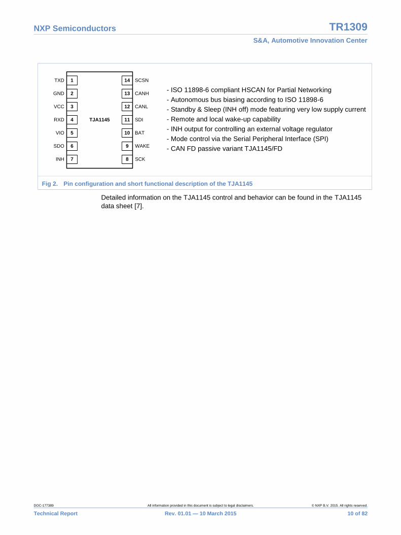
Technical Report Rev. 01.01 — 10 March 2015 10 of 82
1
TJA11454
3
2
5
6
14
11
12
13
10
9
7 8
TXD
GND
VCC
RXD
VIO
SDO
INH
SCSN
CANH
CANL
SDI
BAT
WAKE
SCK
- ISO 11898-6 compliant HSCAN for Partial Networking
- Autonomous bus biasing according to ISO 11898-6
- Standby & Sleep (INH off) mode featuring very low supply current
- Remote and local wake-up capability
- INH output for controlling an external voltage regulator
- Mode control via the Serial Peripheral Interface (SPI)
- CAN FD passive variant TJA1145/FD
Fig 2. Pin configuration and short functional description of the TJA1145
Detailed information on the TJA1145 control and behavior can be found in the TJA1145
data sheet [7].

NXP Semiconductors TR1309 S&A, Automotive Innovation Center
DOC-177389 All information provided in this document is subject to legal disclaimers. © NXP B.V. 2015. All rights reserved.
Technical Report Rev. 01.01 — 10 March 2015 11 of 82
2.2 Hardware application
The figure below shows an example hardware application of the TJA1145.
C
+
CAN
TJA1145
TJA1145/FD
CAN
bus
e.g.
100pF
e.g.
100pF
e.g.
4,7nF
13
12
GND
VDD
TxD
RxD
I/O
4
1
14
3
2
CANH
CANL
TxD
RxD
SCSN
GND
I/O6SDO
** RT
** RT
I/O8SCK
I/O11SDI
Battery
KL30
10
e.g.
47nF
BAT
7
Battery
KL15
e.g. 47k
9WAKE
e.g.
22uF
*
VCC
e.g.
47nF
3V*
VIO
INH
5V
e.g.
47nF
5
Size of capacitor depends on regulator.
For bus line end nodes RT = 60 Ohm in order to support the „Split termination approach“
For stub nodes an optional „weak“ termination of e.g. RT = 1,3kOhm can be foreseen, if required by the OEM.
General remark: A dedicated application may depend on specific OEM requirements.
*
**
10k
10nF
Fig 3. Typical application with the TJA1145
NXP Semiconductors TR1309 S&A, Automotive Innovation Center
DOC-177389 All information provided in this document is subject to legal disclaimers. © NXP B.V. 2015. All rights reserved.
Technical Report Rev. 01.01 — 10 March 2015 12 of 82
2.3 Upgrading a TJA1041 / TJA1043 application, BAT supply
From old applications based on transceivers without CAN Partial Networking functionality
like the TJA1041 and TJA1043 it is known to apply a series resistor in the BAT supply
line of the transceiver. Typical applications where making use of e.g. a 1k series resistor
in the BAT line of the transceiver, which was possible for these parts since the BAT
supply current was very low under all application conditions.
With introducing the TJA1145, such series resistor in the BAT supply shall not be used
anymore, since the supply current of the TJA1145 might get higher temporarily during
start-up of a system. This temporary current would cause some extra voltage drop cross
such a resistor and with that may lead to a non-starting system at low BAT conditions
(e.g. during deep BAT cranking). Since that current is no static current, any kind of cyclic
start-up effects may occur with low battery voltages. This can be avoided with not using
any series resistor as shown in the application diagram in Fig 3.
Background of the temporary extra BAT current are two functions:
- Internal BOOT sequence of the IC
- VCC RAM retention feature, used for SBC variants on the same die
The BOOT sequence is used to copy data from internal Non Volatile Memory (NVM) into
the digital core of the transceiver distinguishing various features on the chip. Such a copy
needs an internal small state engine to be active consuming some extra current for a few
ms (typ 4ms). The transceiver enters its normal operating behavior with successful finish
of the BOOT sequence. An interrupted BOOT sequence (e.g. due to under-voltage event
on BAT) is repeated until successfully completed.
The VCC RAM retention feature is a function used for the SBC variants from the same
die. If the VCC supply of the system was present once, the RAM retention function tries
to keep the VCC supply present as long as possible, especially during deep cranking
condition, if the device is configured to be an SBC. This RAM retention function may get
active as well, if there is a deep BAT cranking condition falling below the BAT under-
voltage detection threshold, even if the device is used as TJA1145 transceiver. So, if
VCC of the application was present before cranking and the BAT supply drops, the RAM
retention function consumes about 10mA (typ) up to 25mA from the BAT pin at start-up
and would become visible with typically 4V output voltage on VCC. Such a temporary
extra current would cause a significant voltage drop cross an external series resistor in
the BAT line and may force a cyclic start-up behavior during deep cranking. This can be
easily avoided with direct connection of the BAT supply input with the battery supply of
the application as shown in Fig 3.

NXP Semiconductors TR1309 S&A, Automotive Innovation Center
DOC-177389 All information provided in this document is subject to legal disclaimers. © NXP B.V. 2015. All rights reserved.
Technical Report Rev. 01.01 — 10 March 2015 13 of 82
3. Microcontroller Interface
3.1 SPI
The SPI interface is the main communication channel between the TJA1145 and the
microcontroller. Using the SPI interface, the microcontroller configures the TJA1145 and
reads back status information. Communication speed is at most 1Mbps, when the device
is in sleep, otherwise 4Mbps.
3.1.1 Functionality of the SPI pins
The TJA1145 is controlled via the 4-wire SPI interface as shown in Fig 4. It consists of
four digital pins:
- Serial Data Input (SDI)
- Serial Data Output (SDO); floating when SCSN is HIGH
- SPI clock in (SCK); default input level shall be LOW due to low-power-concept
- SPI Chip Select (SCSN); active LOW
The SPI connections can optionally be applied with e.g. 1k series-resistors that may
help to reduce EMC emission, especially if there is a long distance between the host
controller and the TJA1145.
To ensure that the SCSN pin and the SCK pin are always on a defined level, the
TJA1145 contains an internal pull-up resistor to VIO at SCSN and an internal pull-down
resistor to GND at SCK. Pin SDO is driven by an internal push-pull output that is only
active if the SCSN pin is LOW. Otherwise the SDO pin is floating. Therefore, it is possible
to connect another SPI device in parallel if it has an own chip select pin.
Sta
nd
ard
µC
Po
rts
Micro-
controller1k*
1k*
1k*
* optional
UJA107
x
SCSN
SDI
SDO
SCK
Typ
60k
Typ
60k
VIO VCC
1k*
TJA1145
Fig 4. SPI interface

NXP Semiconductors TR1309 S&A, Automotive Innovation Center
DOC-177389 All information provided in this document is subject to legal disclaimers. © NXP B.V. 2015. All rights reserved.
Technical Report Rev. 01.01 — 10 March 2015 14 of 82
Fig 5 shows an example configuration when an additional SPI device is connected in
parallel to the same microcontroller SPI interface. Except for the SCSN all pins can be
shared between the TJA1145 and the second slave, provided that the SDO of the
second slave is also floating when its SCSN is HIGH. This configuration can be extended
by other SPI devices that also have SDO pins with the same characteristic.
Sta
nd
ard
µC
Po
rts
Micro-
controller
SCSN
SDI
SDO
SCK
VIO VCC
TJA1145
Slave 2
SDO
SCSN
SCK
SDI
Fig 5. SPI configuration if two slaves are connected to the same MCU SPI Interface
It should be noted, that the microcontroller input/output lines connected to SDO/SDI shall
provide a weak pull-up or pull-down behavior in order to avoid a floating net while SCSN
is HIGH. If the microcontroller port does not provide such pull-up or pull-down it is
recommended to add an external resistor here in order to avoid extra quiescent current
caused by a floating net.
3.1.2 Configuration of the SPI Interface
The TJA1145 SPI interface can be used for 16-, 24- or 32 bit SPI read/write accesses.
The TJA1145 tolerates also SPI messages with more than 32 bits during a read
operation, but only the first 32 bits are considered. In this case the SDI is reflected on
SDO from bit 33 onwards. SPI messages with less than 16 bits are completely ignored.
Fig 6 shows how the SPI interface has to be configured. The TJA1145 shifts data with
the rising edge and samples with the falling edge of the pin SCK. The initial setting on the
microcontroller side of SCK when SCSN goes down shall be LOW. Furthermore, the
TJA1145 expects that the most significant bit is sent first. Any SPI access is a

NXP Semiconductors TR1309 S&A, Automotive Innovation Center
DOC-177389 All information provided in this document is subject to legal disclaimers. © NXP B.V. 2015. All rights reserved.
Technical Report Rev. 01.01 — 10 March 2015 15 of 82
bidirectional data transfer. As one bit is written into SDI, another bit is shifted out of SDO
(see Fig 6).
SCSN
SCK
SDI
SDO
01 02 03
X MSB
sampled
14 13 12
03
X MSB 14 13 12
n-1 n
01 LSB X
01 LSBfloating floating
Fig 6. Configuration of SPI interface, example with 16-bit access
3.1.3 SPI Register Architecture
The SPI allows for full duplex data transfer, meaning that status information is returned
when new control data is shifted in. Fig 7 shows the register structure of the TJA1145.
The upper seven bits of the 16-, 24- or 32-bit SPI message determine which register is
addressed. Bit number 8 contains the ‘Read-Only’ bit (the LSB). The ‘Read Only’ bit
(RO), determines whether something is actually written into the addressed register(s) or
not. Hence, this bit allows a read-only access option where registers are read back by
the application without changing the register content. If this bit is set to 1 the SPI transfer
is a read-only access and all data bits (bit 0 to n) written into SDI are ignored. If the RO
bit is 0, the data bits (bit 0 to n) are written into the addressed register. The written data
become valid as soon as the SCSN pin returns back to HIGH level.

NXP Semiconductors TR1309 S&A, Automotive Innovation Center
DOC-177389 All information provided in this document is subject to legal disclaimers. © NXP B.V. 2015. All rights reserved.
Technical Report Rev. 01.01 — 10 March 2015 16 of 82
0x00 0x01 0x02 0x03 0x04 0x05 0x06
ID =
0x03data data data
Addressable data range of the TJA1145
the TJA1145 accepts 16-, 24- or 32-bit
SPI messages
A6 A5 A4 A3 A2 A1 A0 RO X X X X X X X X
0x07 0x7D 0x7E 0x7F
Identifier byte Data byte
data bitsaddress bits read-only bit
Fig 7. Structure of SPI register
Within a 16-bit SPI access, the first 7 bits determine the addressed register; bit number 8
determines whether a read-only or read/write access is request. Byte two (bits 9 to 16)
represents the data to be written into the addressed register in case of RO = 0.
Within a 32-bit SPI access the first 7 bits determine the first addressed register; bit
number 8 determines whether a read-only or read/write access is request. Bytes two to
four (bits 9 to 32) represent the data to be written into the addressed registers in case of
RO = 0. The register address is automatically incremented.
The TJA1145 also tolerates attempts to write to registers that do not exist. The
corresponding data is lost in that case. If the available address space is exceeded during
a write operation (possible only with a 24 or 32 bit access), the data overflows into
address 0x00 and potentially the following addresses.
During a write operation, the TJA1145 monitor the number of SPI bits transmitted. If the
number does not fit 16, 32 or 32, then the write operation gets aborted and an SPI failure
event is captured in the SPIF (SPI Failure) bit in the System event status register
(address 0x61) if the according event capturing got enabled by the SPIFE (SPI Failure
Enable) bit.
Remark: An SPI Failure event is also captured in case of writing an illegal code to the
MC (Mode Control) bits as well as with the attempt to write access to a locked register.
An SPI failure is not captured in Sleep Mode (see chapter 3.2 for more details on failure
event detection).
The following tables give an overview on the SPI register map of the TJA1145. Note that
the SPI addresses and bit positions are the same for equal functionalities in the TJA1145

NXP Semiconductors TR1309 S&A, Automotive Innovation Center
DOC-177389 All information provided in this document is subject to legal disclaimers. © NXP B.V. 2015. All rights reserved.
Technical Report Rev. 01.01 — 10 March 2015 17 of 82
and the complete UJA116x SBC family (family approach; also NXPs UJA113x family
offers the same main SPI register architecture).
Table 2. General Register Map (valid for all: TJA1145)
Address Bits A6 to A0 Register (Read/Write depending on RO)
Primary Control Registers
0x01 000 0001 Mode Control
0x03 000 0011 Main Status
0x04 000 0100 System Event Enable
General Purpose Memory and Lock Control Registers
0x06 000 0110 Memory 0
0x07 000 0111 Memory 1
0x08 000 1000 Memory 2
0x09 000 1001 Memory 3
0x0A 000 1010 Lock Control
CAN Transceiver Registers
0x20 010 0000 CAN Control
0x22 010 0010 Transceiver Status
0x23 010 0011 Transceiver Event Enable
Event Capture Registers
0x60 110 0000 Global Event Status
0x61 110 0001 System Event Status
0x63 110 0011 Transceiver Event Status
0x64 110 0100 WAKE Pin Event Status
Identification Register
0x7E 111 1110 Identification
WAKE Pin Registers
0x4B 100 1011 WAKE Pin Status
0x4C 100 1100 WAKE Pin Enable
CAN Partial Networking Registers
0x26 010 0110 Data Rate
0x27 010 0111 Identifier 0

NXP Semiconductors TR1309 S&A, Automotive Innovation Center
DOC-177389 All information provided in this document is subject to legal disclaimers. © NXP B.V. 2015. All rights reserved.
Technical Report Rev. 01.01 — 10 March 2015 18 of 82
Address Bits A6 to A0 Register (Read/Write depending on RO)
0x28 010 1000 Identifier 1
0x29 010 1001 Identifier 2
0x2A 010 1010 Identifier 3
0x2B 010 1011 Mask 0
0x2C 010 1100 Mask 1
0x2D 010 1101 Mask 2
0x2E 010 1110 Mask 3
0x2F 010 1111 Frame Control
0x68 110 1000 Data Mask 0
0x69 110 1001 Data Mask 1
0x6A 110 1010 Data Mask 2
0x6B 110 1011 Data Mask 3
0x6C 110 1100 Data Mask 4
0x6D 110 1101 Data Mask 5
0x6E 110 1110 Data Mask 6
0x6F 110 1111 Data Mask 7
3.2 Wake-up and interrupt event diagnosis via pin RXD in CAN Offline
3.2.1 Overview of events
The TJA1145 offers the ability to feedback to the application if conditions apply to the
TJA1145 which might be important for the application either to provoke a wake-up from
Standby or Sleep Mode or signal interrupts to the running application in case certain
conditions are changed which e.g. exceed critical values or are important for the
application to perform next steps.
The tables below show all supported regular wake-up events and interrupt events of the
TJA1145. The event name is given followed by a short description when such an event is
detected. Column three explains whether detection of specific events is enabled after
initial BAT power-on or whether it needs to be actively enabled. This is useful for
selection of dedicated interrupt event detection based on the application need. Some
interrupt events are always enabled (e.g. power-on (PO)).

NXP Semiconductors TR1309 S&A, Automotive Innovation Center
DOC-177389 All information provided in this document is subject to legal disclaimers. © NXP B.V. 2015. All rights reserved.
Technical Report Rev. 01.01 — 10 March 2015 19 of 82
Table 1. Regular wake-up events
Event Description Default function after
power-on
CAN wake-up
(CW)
A CAN wake-up was detected, either
- Standard wake-up pattern in CAN Offline or
- Selective wake-up frame (only if selective wake-up enabled)
off
Rising WAKE edge
(WPR)
Rising edge on pin WAKE detected off
Falling WAKE edge
(WPF)
Falling edge on pin WAKE detected off
Table 2. Interrupt Events
Event Description Default function after
power-on
Power-on
(PO)
The TJA1145 has exited Off Mode
(Rising BAT voltage passed Vth(det)pon)
always on
CAN bus silence
(CBS)
No activity on CAN bus for tto(silence) off
CAN failure
(CF)
A CAN failure was detected, either
- CAN transceiver deactivated due to VCC undervoltage (only if CMC = 01)
or
- CAN transceiver deactivated due to a dominant clamped TXD pin
(only captured if CAN in Active Mode)
off
SPI failure
(SPIF)
A SPI failure was detected, either
- SPI clock count error or
- Illegal MC code
- Write attempt to locked registers
off
Over temperature
warning
(OTW)
The IC temperature exceeded Tth(warn)ot off
Partial Networking
Frame Detection
Error
(PNFDE)
Partial networking frame detection error detected
(only if selective wake-up enabled)
always on
3.2.2 Event control & detection
All events (except PO and PNFDE) can be can be enabled or disabled via the Event
Capture Enable Registers:
- System event capture enable register (0x04)

NXP Semiconductors TR1309 S&A, Automotive Innovation Center
DOC-177389 All information provided in this document is subject to legal disclaimers. © NXP B.V. 2015. All rights reserved.
Technical Report Rev. 01.01 — 10 March 2015 20 of 82
- Transceiver event capture enable register (0x23)
- WAKE pin event capture enable register (0x04)
where a ‘1’ means capturing enabled while a ‘0’ means capturing disabled.
In case an enabled capture function detects an event the following happens:
- The relevant event status bit is set (address range 0x61 to 0x64)
- In case CAN is in Offline Mode the RXD pin is forced LOW
- If the TJA1145 is in Sleep Mode a transition to Standby Mode is performed
including activation of the INH pin
Monitoring of events can be done by regular polling of the event status bits in the
registers 0x61 to 0x64, e.g. when CAN is Active or Listen-only and thus event detection
would not generate a LOW level on pin RXD. In order to allow a shorter polling time the
TJA1145 offers the Global Event Status Register at address 0x60, summarizing whether
and which of the other registers have an event status bit currently set.
Clearing event status bits in registers 0x61 to 0x64 can be done by writing a 1 to the
relevant bit (writing a 0 will have no effect). During one write access also several status
bits can be cleared, if needed.
3.2.3 Limiting microcontroller disturbance by events
In order to limit the impact on the software processing time, an event delay timer is
incorporated for pin RXD. Whenever a pending event status bit is cleared while the CAN
block is in CAN Offline Mode the pin RXD is released to HIGH and an internal delay timer
(td(event)) starts running. Pin RXD will not go LOW again before td(event) overflows even if
there is another pending event or a event gets captured just during td(event). Nevertheless
the event status bits can be read and cleared at any time.
The timer gets stopped immediately when Sleep Mode gets entered. If on top at entering
Sleep Mode an event is still pending this is immediately shown by a LOW level at RXD
indicating the wake-up from Sleep as described in the following chapter.
3.2.4 Sleep Mode protection
A distinction is made regarding regular wake-up events (Table 1) and interrupts (Table
2). In order to be able to wake-up the TJA1145 from Sleep Mode the application needs to
enable at least one of the regular wake-up events (via pin WAKE or the CAN bus) before
entering Sleep Mode in order to avoid a deadlock situation in which the TJA1145 could
not be woken up by external sources. Entering Sleep Mode requires as well clearing of
all pending events.
If one of those two conditions is not met, the TJA1145 will perform a transition to Standby
Mode instead as a reaction on a Sleep Mode attempt.

NXP Semiconductors TR1309 S&A, Automotive Innovation Center
DOC-177389 All information provided in this document is subject to legal disclaimers. © NXP B.V. 2015. All rights reserved.
Technical Report Rev. 01.01 — 10 March 2015 21 of 82
4. CAN transceiver Interface
4.1 High speed CAN basics
The core function of the TJA1145 is transmission and reception of CAN signals via the
two bus pins CANH and CANL and to the protocol controller via the pins TXD and RXD.
The protocol controller outputs a serial transmit data stream to the TXD input of the
TJA1145. An internal pull-up function drives the TXD input to logic HIGH if unconnected,
which means that the bus output driver stays recessive in this fault scenario. In the
recessive state (Fig 8) the CANH and CANL pins are biased to a voltage level of VCC
divided by 2. If a logic LOW level is applied to TXD, the output stage is activated,
generating a dominant state on the bus line (Fig 8).
time
Differential
Bus Voltage
Single Ended
Bus Voltage
-1.0V
0.5V
0.9V
5.0V
Recessive Dominant Recessive
1.4V
2.5V
3.6VCANH
CANL
Differential input voltage
range for dominant state
Differential input voltage
range for recessive state
Fig 8. Nominal bus levels according to ISO11898
If no bus node transmits a dominant bit, the bus stays in recessive state. If one or
multiple bus nodes transmit a dominant bit, then the bus lines enter the dominant state
overriding the recessive state (wired-AND characteristic).
The receiver converts the differential bus signal to a logic level signal, which is output at
RXD. The serial receive data stream is provided to the bus protocol controller for
decoding. The internal receiver comparator is always active. It monitors the bus while the
bus node is transmitting a message. This is required to support the non-destructive bit-
by-bit arbitration scheme of CAN.
NXP Semiconductors TR1309 S&A, Automotive Innovation Center
DOC-177389 All information provided in this document is subject to legal disclaimers. © NXP B.V. 2015. All rights reserved.
Technical Report Rev. 01.01 — 10 March 2015 22 of 82
Details about high speed CAN applications in general are explained in the NXP
application hints document “Rules and recommendations for in-vehicle CAN
networks” [8].
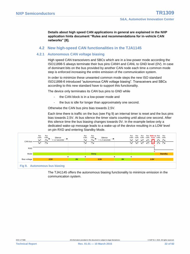
4.2 New high-speed CAN functionalities in the TJA1145
4.2.1 Autonomous CAN voltage biasing
High speed CAN transceivers and SBCs which are in a low-power mode according the
ISO11898-5 always terminate their bus pins CANH and CANL to GND level (0V). In case
of dominant bits on the bus provided by another CAN node each time a common mode
step is enforced increasing the entire emission of the communication system.
In order to minimize these unwanted common mode steps the new ISO standard
ISO11898-6 introduced “autonomous CAN voltage biasing”. Transceivers and SBCs
according to this new standard have to support this functionality.
The device only terminates its CAN bus pins to GND while
- the CAN block is in a low-power mode and
- the bus is idle for longer than approximately one second.
Otherwise the CAN bus pins bias towards 2,5V.
Each time there is traffic on the bus (see Fig 9) an internal timer is reset and the bus pins
bias towards 2,5V. At bus silence the timer starts counting until about one second. After
this silence time the bus biasing changes towards 0V. In the example below only a
dedicated wake-up message leads to a wake-up of the device resulting in a LOW level
on pin RXD and entering Standby Mode.
Bus
traffic
Bus
traffic
Bus
traffic
Bus
traffic
Bus
traffic
Bus
traffic
Bus
traffic
Bus
traffic
Wake-up
frame
Bus
traffic
Bus
trafficSilence
< 1.2 seconds
Silence
< 1.2 secondsCAN bus
RXD
Mode
Bias voltage
Sleep Standby
2.5V 0V 2.5V 0V 2.5V
Fig 9. Autonomous bus biasing
The TJA1145 offers the autonomous biasing functionality to minimize emission in the
communication system.

NXP Semiconductors TR1309 S&A, Automotive Innovation Center
DOC-177389 All information provided in this document is subject to legal disclaimers. © NXP B.V. 2015. All rights reserved.
Technical Report Rev. 01.01 — 10 March 2015 23 of 82
4.2.2 Partial networking
Besides autonomous biasing, the core feature of the ISO11898-6 standard is the
“selective wake-up” functionality of a CAN device in order to allow “partial networking” in
a CAN bus system.
Partial networking is the ability of a network to allow only a sub group of nodes to actively
communicate, while the remaining nodes are inactive and in a low-power mode watching
the bus traffic for a wake-up message.
Upon reception of a wake-up message the CAN device can activate the entire node.
Such wake-up messages may address nodes individually or as a group.
The functionality, which is needed in the transceivers for this kind of network operation, is
called “selective wake-up”.
The decision to stop active communication of a node needs to be made on application
software level and is thus controlled by the microcontroller and not by the CAN device.
Partial Networking is to support following use cases:
- Saving power and reducing CO2:
CAN nodes which offer functionality which is not constantly required like e.g.
auxiliary heating, seat heating, and trailer interface can be set into Sleep Mode
with selective wake-up instead of being active on the bus and wasting power.
- Minimizing wake-up lines and relays:
In today’s cars partially used CAN nodes are activated / deactivated by additional
wake-up lines and relays (un-powering nodes). Using partial networking allows
getting rid of this extra hardware and wiring, reducing cost, weight and enabling
higher flexibility in terms of partial networking use case scenarios.
- Reducing ECU operation and up times:
Partially running the CAN bus nodes (except of the CAN transceiver) in Sleep
Mode reduces the up time of components in the module like voltage regulators,
capacitors, microcontrollers. This offers a high advantage especially for hybrid and
electrical vehicles, where the battery charging time adds to the driving cycle. By
use of partial networking it may be avoided to specify longer up times for modules
that do not need to take part in the communication related to battery charging.
Both TJA1145 variants offer the selective wake-up functionality to support and build up
partial networking networks.
Further details about partial networking are explained in the NXP application hints
document “Partial Networking in high speed CAN networks” [9].
4.2.3 CAN FD passive
In 2012, Bosch proposed a new frame format called CAN FD that allows more than 8
bytes of data per frame and moreover a higher bit rate in the data field than in the
arbitration field. This is not backward compatible to ISO11898-1:2003 (defining the CAN
protocol) and thus CAN FD frames cannot be decoded by partial networking
transceivers. A CAN FD frame would cause decoding errors within a typical partial
networking capable transceiver and thus leads to unintended wake-up in case of too
many CAN FD frames are interleaved with classic CAN frames on the bus.

NXP Semiconductors TR1309 S&A, Automotive Innovation Center
DOC-177389 All information provided in this document is subject to legal disclaimers. © NXP B.V. 2015. All rights reserved.
Technical Report Rev. 01.01 — 10 March 2015 24 of 82
To facilitate simple migration towards CAN FD adoption, NXP offers an innovative new
feature, used in combination with partial networking. This allows nodes which only
support standard high speed CAN controllers to remain in sleep (or standby) while
CAN FD frames are transmitted on the bus, without generating bus errors. An ISO11898-
6 (partial networking) compliant device still can be woken by the configured wake-up
frames in the classic CAN frame format according ISO11898-1:2003.
CAN FD passive CAN modules, which are not equipped with a CAN FD capable CAN
controller, can be set to Sleep or Standby, while other nodes communicate using CAN
FD frames. Offering CAN FD tolerance is the only way to operate a network with a
mixture of CAN and CAN FD controllers.
The TJA1145/FD variant offers CAN FD passive behavior allowing other nodes to send
CAN FD frames on the bus.
Further details about CANFD tolerance are explained in the NXP application hints
document “Partial Networking in high speed CAN networks” [9].
4.3 CAN Transceiver Overview
The TJA1145 includes a high speed CAN transceiver compliant to the ISO11898-6
standard.
The CAN transmitter is supplied by the external VCC supply pin. Fig 10 shows the
operating voltage range of VCC for the CAN transmitter. The CAN transmitter is fully
specified between 4.75V≤VVCC≤5.5V for a CAN termination between 45Ω and 65Ω.
During CAN Active mode also the recessive bias voltage is derived from VCC.
The CAN receiver is supplied directly from the BAT supply pin.
CAN offline
4.25V
4.75VCAN supply (VCC) undervoltage
detection & recovery
CAN fully specified @ 45-65Ω
CAN functional specified (some
parameters out of spec)5.5V
0V
6V
Fig 10. CAN transmitter VCC operating range
NXP Semiconductors TR1309 S&A, Automotive Innovation Center
DOC-177389 All information provided in this document is subject to legal disclaimers. © NXP B.V. 2015. All rights reserved.
Technical Report Rev. 01.01 — 10 March 2015 25 of 82
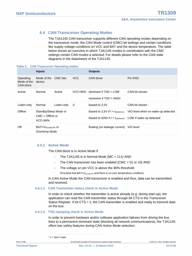
4.4 CAN Transceiver Operating Modes
The TJA1145 CAN transceiver supports different CAN operating modes depending on
the transceiver mode, the CAN Mode control (CMC) bit settings and certain conditions
like supply voltage conditions on VCC and BAT and the device temperature. The table
below shows an overview in which TJA1145 modes in combination with the CMC
settings certain CAN modes a selected. For details please refer to the CAN state
diagrams in the datasheets of the TJA1145.
Table 3. CAN Transceiver Operating modes
Inputs Outputs
Operating
Mode of the
CAN block
Mode of the
device
CMC bits VCC CAN driver Pin RXD
Active Normal Active VCC>90% dominant if TXD = LOW CAN bit stream
recessive if TXD = HIGH
Listen-only Normal Listen-only x1 biased to 2,5V CAN bit stream
Offline
Standby/Sleep Mode or
CMC = Offline or
VCC<90%
biased to 2,5V if t < tto(silence) VIO level when no wake-up detected
biased to GND if t > tto(silence) LOW if wake-up detected
Off BAT<Vth(uvd)CAN or
Overtemp Mode
floating (no leakage current) VIO level
4.4.1 Active Mode
The CAN block is in Active Mode if
- The TJA1145 is in Normal Mode (MC = 111) AND
- The CAN transceiver has been enabled (CMC = 01 or 10) AND
- The voltage on pin VCC is above the 90% threshold
(Provided that BAT<Vth(uvd)CAN and there is no over temperature condition)
In CAN Active Mode the CAN transceiver is enabled and thus, data can be transmitted
and received.
4.4.1.1 CAN Transmitter status check in Active Mode
In order to check whether the transmitter is active already (e.g. during start-up), the
application can read the CAN transmitter status through bit CTS in the Transceiver
Status Register. If bit CTS = 1, the CAN transmitter is enabled and ready to transmit data
on the bus.
4.4.1.2 TXD clamping check in Active Mode
In order to prevent hardware and/or software application failures from driving the bus
lines to a permanent dominant state (blocking all network communications), the TJA1145
offers two safety features during CAN Active Mode selection:
1 x = don´t care

NXP Semiconductors TR1309 S&A, Automotive Innovation Center
DOC-177389 All information provided in this document is subject to legal disclaimers. © NXP B.V. 2015. All rights reserved.
Technical Report Rev. 01.01 — 10 March 2015 26 of 82
- Entering CAN Active is possible only while the TXD pin is HIGH. If pin TXD pin is
LOW at CAN Active selection, the SBCs will not enable the transmitter until TXD
was first released HIGH again.
- During CAN Active, a LOW level on pin TXD that persists longer than tto(dom)TXD
will disable the transmitter, releasing the bus lines to recessive state.
If the TXD dominant timeout time is exceeded, this will be indicated as well as a
CAN failure in bit CFS in the Transceiver Status Register. Additionally, the CF bit
in the Transceiver event status register will be set in case this interrupt is
enabled via bit CFE.
Note that pin TXD is internally pulled-up (towards VIO) to ensure a recessive condition in
Active Mode on the bus in case the pin is left floating.
CAN
Offline
CAN
Active
CAN
Listen-
only
CAN
OffOff or Over-
temp Mode
Normal Mode AND
CMC = Active
CMC = Active
CMC = Listen-only
Normal Mode AND
CMC = Active
Standby / Sleep Mode OR
CMC = Offline
leaving Off or
Overtemp
Fig 11. Simplified CAN state diagram (while VCC>90% nom. voltage)
4.4.2 Listen-only Mode
The CAN block is in Listen-only Mode if:
- The TJA1145 is in Normal Mode (MC = 111) AND
- The CAN receiver only has been enabled (CMC = 11)

NXP Semiconductors TR1309 S&A, Automotive Innovation Center
DOC-177389 All information provided in this document is subject to legal disclaimers. © NXP B.V. 2015. All rights reserved.
Technical Report Rev. 01.01 — 10 March 2015 27 of 82
(Provided that BAT<Vth(uvd)CAN and no over temperature condition consists)
In CAN Listen-only, the normal CAN receiver is enabled while the CAN transmitter is
disabled.
This facility could be used by development tools that need to listen to the bus, but do not
need to transmit or receive data or for software driven selective wake-up. Dedicated
microcontrollers could be used for selective wake-up, providing an embedded low power
CAN engine designed to monitor the bus for potential wake-ups.
4.4.3 Offline Mode with Autonomous Bus Biasing
The CAN block is in Offline Mode if
- The TJA1145 is in Standby / Sleep Mode OR
- CAN has been actively disabled (CAN = 00) OR
- The CAN supply (VCC) is below 90% of its nominal value while CMC = 01
(Provided that BAT<Vth(uvd)CAN and no over temperature condition consists)
In CAN Offline Mode, the transceiver monitors the CAN bus for a wake-up, provided CAN
wake-up detection is enabled (CWE = 1) in the Transceiver Event Enable Register.
The TJA1145 offers autonomous bus biasing. The device only terminates its CAN bus
pins to GND while
- CAN is Offline Mode AND
- The CAN bus is idle for longer than tto(silence), which is approximately one second.
Otherwise the CAN bus pins bias towards 2,5V. See Fig 12 for the autonomous bus
biasing principal.
4.4.3.1 Entering Sleep Mode at CAN bus silence only
If the tto(silence) timer is expired, this will be indicated in bit CBSS in the Transceiver Status
Register. Additionally, the CBS bit in the Transceiver event status register will be set in
case this interrupt is enabled via bit CBSE.
The CAN bus silence event capturing can be useful in case the TJA1145 is set to
Standby Mode while CAN traffic persists in order to notify the application in case the bus
comes to complete silence; e.g. allowing the ECU to enter sleep mode.

NXP Semiconductors TR1309 S&A, Automotive Innovation Center
DOC-177389 All information provided in this document is subject to legal disclaimers. © NXP B.V. 2015. All rights reserved.
Technical Report Rev. 01.01 — 10 March 2015 28 of 82
0
Bias GND
1
Bias GND
2
Bias GND
3
Bias 2,5V
4
Bias 2,5V
Off
floating
VBAT
> Vth(uvr)CAN
Bus dominant
> twake(dom)bus
Bus recessive
> twake(rec)bus
Bus dominant
> twake(dom)bus
Entering
CAN Active
Bus recessiveBus dominant
tto(wake)bus expired
tto(wake)bus expired
tto(silence) expired AND
CAN Offline
tto(silence) expired AND
CAN Offline
0
Bias GND
Bus recessive
tto(wake)bus = ~700us
twake(dom)bus = twake(rec)bus = 0.5µs to 3µs
tto(silence) = ~1s
Fig 12. Autonomous bus biasing
4.4.3.2 Standard CAN wake-up in Offline Mode
A dedicated wake-up sequence (specified in ISO11898-5) must be received to wake-up
the TJA1145 from Standby or Sleep Mode via CAN and also to activate CAN biasing to
2,5V. This filtering improves the robustness against spurious wake-up events due to a
dominant clamped CAN bus or dominant phases caused by noise or spikes on the bus.
The wake-up pattern consists of the following sequence on the bus:

NXP Semiconductors TR1309 S&A, Automotive Innovation Center
DOC-177389 All information provided in this document is subject to legal disclaimers. © NXP B.V. 2015. All rights reserved.
Technical Report Rev. 01.01 — 10 March 2015 29 of 82
A dominant phase of at least twake(busdom)
A recessive phase of at least twake(busrec)
A dominant phase of at least twake(busdom)
The complete dominant-recessive-dominant pattern must be completed within tto(wake) to be
recognized as a valid wake-up pattern (see Fig 13). Otherwise, the internal wake-up logic
gets reset and the complete wake-up pattern needs to be re-applied to the low power CAN
receiver in CAN Offline Mode before generating a proper remote wake-up. Pin RXD will
remain recessive until the bus wake-up event has been triggered.
tto(wake)bus
VO(diff)bus
twake(dom)bus twake(dom)bustwake(rec)bus
CANH
CANL
RXD
tto(wake)bus = ~700us
twake(dom)bus = twake(rec)bus = 0.5µs to 3µs
Fig 13. Standard wake-up timing
4.4.3.3 Selective CAN wake-up in Offline Mode
The selective wake-up capability is offered in both TJA1145 variants. In case of selective
wake-up enabled in Standby or Sleep Mode, the autonomous biasing is still active as
described in the previous chapter upon reception of a standard CAN wake-up.
Nevertheless, this does not lead to trigger a bus wake-up until a so-called complete CAN
wake-up frame is detected that fits to the pre-configuration in the CAN partial networking
registers of the TJA1145.
Further details about partial networking and the configuration capabilities of the
TJA1145 are explained in the NXP application hints document “Partial Networking
in high speed CAN networks” [9].
4.4.4 Off Mode
The CAN Transceiver is in Off Mode if the TJA1145 is in Off or Overtemp Mode. In CAN
Off Mode the transceiver is switched off completely with the bus lines floating in order to

NXP Semiconductors TR1309 S&A, Automotive Innovation Center
DOC-177389 All information provided in this document is subject to legal disclaimers. © NXP B.V. 2015. All rights reserved.
Technical Report Rev. 01.01 — 10 March 2015 30 of 82
behave passive to the remaining bus, e.g. if the ECU is unsupplied, but still physically
connected to the bus.
4.4.5 CAN supply undervoltage detection
Undervoltage on the CAN transceiver supply pin VCC can be detected depending on the
settings of the CMC bits in CAN Active:
- CMC = 01 CAN Active (with VCAN undervoltage detection enabled)
- CMC = 10 CAN Active (with VCAN undervoltage detection disabled)
Option 1: CMC = 01 undervoltage detection enabled
In case the CAN transceiver is in Active Mode, thus the transmitter and receiver are
enabled and the V1 supply decreases below 90% of its nominal value the TJA1145 takes
the following consequences:
- The CAN transmitter and receiver get disabled CAN Offline Mode entered
- The VCAN supply bit in the Transceiver Status Register indicates an
undervoltage (VCS = 1)
- The CF bit in the Transceiver event status register will be set in case this
interrupt is enabled via bit CFE.
On the automatic recovery of VCC above the 90% threshold, CAN Active get entered
again and the VCAN bit gets cleared automatically.
This feature can be used for automatic disabling the CAN transmitter in case the CAN
supply leaves its allowed operating range and thus the bus level schemes on the CAN
bus do not fully comply to the parameters as being requested by the ISO11898-5 any
longer.
Remark: When the transmitter gets disabled due to a VCC undervoltage condition
while
o a dominant condition on pin TXD is applied and
o the CFE = 1 events are enabled than
pin RXD gets HIGH for ~8us (CAN transmitter got disabled) until RXD gets LOW
again, indicating the captured interrupt of the VCC undervoltage and/or the CAN
failure.
REMARK: Be aware that the VCC undervoltage detection is very precise and might be
able to disable the transmitter immediately in case the VCC drops just below the
undervoltage detection level (e.g. in case of CAN frames being transmitted with too low
buffering on the VCC pin). In case this is unwanted, CMC shall be set to 10 (thus VCC
undervoltage detection gets disabled.
Option 2: CMC = 10 undervoltage detection disabled
NXP Semiconductors TR1309 S&A, Automotive Innovation Center
DOC-177389 All information provided in this document is subject to legal disclaimers. © NXP B.V. 2015. All rights reserved.
Technical Report Rev. 01.01 — 10 March 2015 31 of 82
In case the CAN transceiver is in Active Mode, thus the transmitter and receiver are
enabled and the VCC supply decreases below 90% of its nominal value the TJA1145
takes the following consequences:
- The CAN transmitter and receiver stay enabled until
o the transmitter is not longer capable of transmitting bits on the CAN bus
because of a too low CAN supply
- Both, VCS and CF, do not react on an undervoltage with CMC = 10
This feature can be used in case CAN shall still be functional as long as possible below
the 90% nominal value even without guaranteeing the voltage scheme as requested by
the ISO11898-5.
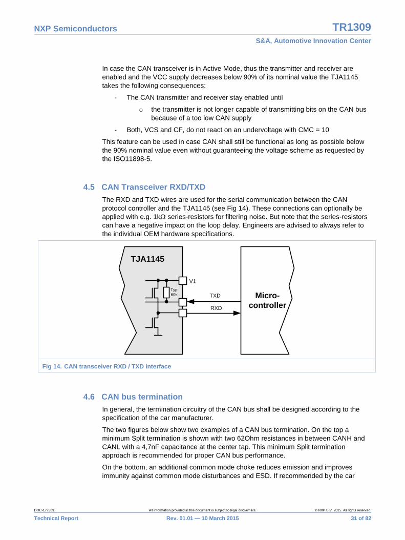
4.5 CAN Transceiver RXD/TXD
The RXD and TXD wires are used for the serial communication between the CAN
protocol controller and the TJA1145 (see Fig 14). These connections can optionally be
applied with e.g. 1k series-resistors for filtering noise. But note that the series-resistors
can have a negative impact on the loop delay. Engineers are advised to always refer to
the individual OEM hardware specifications.
Micro-
controllerRXD
V1
TXDTyp
60k
TJA1145
Fig 14. CAN transceiver RXD / TXD interface
4.6 CAN bus termination
In general, the termination circuitry of the CAN bus shall be designed according to the
specification of the car manufacturer.
The two figures below show two examples of a CAN bus termination. On the top a
minimum Split termination is shown with two 62Ohm resistances in between CANH and
CANL with a 4,7nF capacitance at the center tap. This minimum Split termination
approach is recommended for proper CAN bus performance.
On the bottom, an additional common mode choke reduces emission and improves
immunity against common mode disturbances and ESD. If recommended by the car

NXP Semiconductors TR1309 S&A, Automotive Innovation Center
DOC-177389 All information provided in this document is subject to legal disclaimers. © NXP B.V. 2015. All rights reserved.
Technical Report Rev. 01.01 — 10 March 2015 32 of 82
manufacturer, a common mode choke can be used to reduce the impact of RF-
interferences.
Further details about high speed CAN termination is explained in the NXP
application hints document “Rules and recommendations for in-vehicle CAN
networks” [8].
TJA1145
V1
CANH
CANL
e.g.
100pF
e.g.
100pF
Choke*
PESD1CAN*
CAN Wires
e.g. 4.7nF
e.g.
60
e.g.
60
* optional
TJA1145
V1
CANH
CANL CAN Wires
e.g.
60
e.g.
60
e.g. 4.7nF
(1) Top: example for minimum circuitry needed for full CAN bus functionality
(2) Bottom: example for maximum circuitry with use of common mode choke and ESD protection
Fig 15. Typical Application of the CAN bus pins
4.7 CAN ESD protection
The TJA1145 is designed to withstand ESD pulses up to 8kV according to the Human
Body Model (HBM, C = 100pF, R = 1.5k) and at least 6kV according to the IEC61000-
4-2 (C = 150pF, R = 330) at the bus pins CANH, CANL without external components.
Nevertheless, if higher protection is required, external clamping circuits can be applied to
the CANH and CANL line, e.g. PESD1CAN or PESD2CAN (see Fig 15).

NXP Semiconductors TR1309 S&A, Automotive Innovation Center
DOC-177389 All information provided in this document is subject to legal disclaimers. © NXP B.V. 2015. All rights reserved.
Technical Report Rev. 01.01 — 10 March 2015 33 of 82

NXP Semiconductors TR1309 S&A, Automotive Innovation Center
DOC-177389 All information provided in this document is subject to legal disclaimers. © NXP B.V. 2015. All rights reserved.
Technical Report Rev. 01.01 — 10 March 2015 34 of 82
5. Software Flow
This chapter introduces the software perspective of the TJA1145. It discusses the
different operations, which are used in automotive applications. Fig 16 illustrates the
different operations between “Power-on” and “Power-off”. Moreover, the figure below
provides a quick overview about:
Different kind of operations
Order of the operations
Subchapter, where the operation is discussed in more detail.
Power-onVBAT > 4.5V
Reset
Startup Operation(chapter 5.1)
Normal Operation(chapter 5.2)
Standby Mode requested?
Sleep Mode (chapter 5.3.2)
No
Stop Mode(chapter 5.3.3.1)
Yes
Wake-up
Wait for wake-up event
Wait for interrupt event
RXD Low Handling(chapter 5.3.1.1)
Preparation of In-Vehicle flashing
Low Power Operation Mode
(chapter 5.3)
In-Vehicle Flashing (no change of SBC
MTP configuration)
In-Vehicle Flashing (chapter 5.4)
Fig 16. Abstract view in Software Flow
Example code of all different operations can be found in the appendix chapter 6.3.

NXP Semiconductors TR1309 S&A, Automotive Innovation Center
DOC-177389 All information provided in this document is subject to legal disclaimers. © NXP B.V. 2015. All rights reserved.
Technical Report Rev. 01.01 — 10 March 2015 35 of 82
The figure below shows the simplified state diagram of the TJA1145 from software
perspective. This state diagram will be used in the following subchapters to establish the
link between the different software operations and the related TJA1145 operating modes.
Standby
SleepNormal
SPI command
Wake-up
Power-on
SPI command
SPI command
SPI command
leaving Overtemp
VCC or VIO undervoltage
Fig 17. Simplified mode diagram from SW perspective for TJA1145

NXP Semiconductors TR1309 S&A, Automotive Innovation Center
DOC-177389 All information provided in this document is subject to legal disclaimers. © NXP B.V. 2015. All rights reserved.
Technical Report Rev. 01.01 — 10 March 2015 36 of 82
5.1 Startup Operation
This section introduces the software operations, which are related to the startup of the
application. The Startup Operation takes place in Standby Mode of the TJA1145 and is
executed after “Power-On” or “Wake-up” from Sleep. The figure below shows the
different hardware events that trigger the execution of the Startup Operation. At the end
of the Startup Operation a transition to Normal Operation Mode is performed via the
related SPI command.
Standby
SleepNormal
SPI command
Wake-up
Power-on
SPI command
SPI command
SPI command
leaving Overtemp
VCC or VIO undervoltage
Fig 18. Simplified mode diagram with focus on Startup Operation
The Startup Operation typically consists of the following parts:
- Microcontroller initialization
- Application initialization
- Check of device identification
- In-vehicle Flashing of ECUs (if implemented)
- Check reason of last Sleep Mode (SPI command or VIO /VCC undervoltage)
- Event handling
- Transition to Normal Operation Mode
Fig 19 shows the complete flow of the Startup Operation with its different parts.
Moreover, it guides to the related subchapter for a detailed explanation.

NXP Semiconductors TR1309 S&A, Automotive Innovation Center
DOC-177389 All information provided in this document is subject to legal disclaimers. © NXP B.V. 2015. All rights reserved.
Technical Report Rev. 01.01 — 10 March 2015 37 of 82
System Reset
Init MCU(chapter 5.1.1)
In-Vehicle Flashing (chapter 5.4)
YesFlash
programming?(chapter 5.1.4)
Event Handling(chapter 5.1.6)
Start Normal Operation (chapter 5.1.7)
Get Device ID
No
Yes
Init Application(chapter 5.1.2)
SW running for correct hardware?
Yes
End of Startup OperationNo
Check Device ID (chapter 5.1.3)
Check FSMS (chapter 5.1.5)
Fig 19. Startup Operation Software Flow

NXP Semiconductors TR1309 S&A, Automotive Innovation Center
DOC-177389 All information provided in this document is subject to legal disclaimers. © NXP B.V. 2015. All rights reserved.
Technical Report Rev. 01.01 — 10 March 2015 38 of 82

NXP Semiconductors TR1309 S&A, Automotive Innovation Center
DOC-177389 All information provided in this document is subject to legal disclaimers. © NXP B.V. 2015. All rights reserved.
Technical Report Rev. 01.01 — 10 March 2015 39 of 82
5.1.1 Microcontroller initialization
The microcontroller initialization is always the first part of the startup routine. It is a
microcontroller specific routine that configures the microcontroller and its periphery. With
respect to the TJA1145 transceiver, at least it has to be insured that after the initialization
the SPI periphery of the microcontroller is working properly. Otherwise no communication
with the TJA1145 can take place.
5.1.2 Application initialization
The application initialization is also necessary at the beginning of the startup routine. It is
an application specific routine that initializes the global application specific variables.
Hence, it is insured that after the initialization the application software is working
properly. Otherwise e.g. the scheduler or counters are not working correctly.
5.1.3 Check device identification
In order to check, if the running application software is used for the correct hardware
device type, the identification register is read and the TJA1145 type is determined. This
is required to ensure that the software runs on the correct hardware.
5.1.4 Flash programming
Here it is checked whether a re-flashing of the microcontroller is requested (flash
signature invalid) or not. In case the microcontroller must be flashed, Startup Operation is
aborted and Flash programming (see chapter 5.4) is started.
5.1.5 Check reason for entering Sleep Mode before
In order to check, if the transceiver has been forced to Sleep Mode before due to
undervoltage event, the FSMS bit in the Main Status Register is read. If FSMS is set, the
transition to Sleep Mode has been forced by a VCC or VIO undervoltage and CAN wake-
up, local wake-up via the WAKE pin have been enabled and Partial Networking has been
disabled (CPNC = 0). Hence if FSMS is set, the initialization configuration shall be
restored in Startup Operation.

NXP Semiconductors TR1309 S&A, Automotive Innovation Center
DOC-177389 All information provided in this document is subject to legal disclaimers. © NXP B.V. 2015. All rights reserved.
Technical Report Rev. 01.01 — 10 March 2015 40 of 82
5.1.6 Event Handling during Startup
As several events might have caused a reset and rather the Startup Operation, all
pending events should be read, handled and cleared in during startup. As long as the
CAN transceiver is not in Active or Listen-only Mode, the RXD pin signals whether an
event is pending or not. If events are pending after Startup Operation and CAN is not in
Active or Listen-only Mode, the RXD pin connected to the CAN Controller cannot trigger
any further software actions because it remains low.
It must be ensured that all event sources are cleared (to release RXD) and that an
initialization of the TJA1145 has been performed. If the Power-On event is set, the reset
was caused by leaving the Off-state. In this case the TJA1145 must be initialized, which
means an initial configuration of:
- CAN Transceiver incl. Partial Networking, if desired
- General Purpose Memories
- System events
- Transceiver events
- Wake pin events
Additionally, if desired, the configuration can be locked by writing to the related bits in the
Lock Control Register (register address 0x0A). For that reason it is possible to only lock
the partial networking configuration registers and allow write access to the other registers
at any point in time.
The event handling in Startup Operation Mode does not differ from the Event Polling and
Handling done during Normal Operation. For that reason further information on that topic
incl. software flows can be found in chapter 0.
5.1.7 Transition to Normal Mode
Normal Mode is entered by writing 0x07 to the Mode Control Register. For more
information on Normal Operation refer to chapter 0.

NXP Semiconductors TR1309 S&A, Automotive Innovation Center
DOC-177389 All information provided in this document is subject to legal disclaimers. © NXP B.V. 2015. All rights reserved.
Technical Report Rev. 01.01 — 10 March 2015 41 of 82
5.2 Normal Operation
This section introduces the software operations which are associated to Normal
Operation of the application. Normal Operation is related to the Normal Mode of the
TJA1145. This mode can only be entered after a successful Startup Operation. Therefore
the beginning of Normal Operation is a transition from Standby to Normal Mode caused
by the related SPI command.
Standby
SleepNormal
SPI command
Wake-up
Power-on
SPI command
SPI command
SPI command
leaving Overtemp
VCC or VIO undervoltage
Fig 20. Simplified mode diagram with focus on Normal Operation
The most important operations of the Normal Operation are the transceiver control,
polling for events and the execution of the application. For that reason this chapter shows
how to enable the CAN Transceiver and poll transceiver for events. At the end of the
Normal Operation a transition to Low Power Operation (Standby, Sleep) is performed via
the related SPI command.
Fig 20 shows the different parts of Normal Operation. It consists of:
- Enter Normal Operation
- CAN Transceiver control
- Event Handling
- Run default application
- Transition to Low Power Operation (Standby, Sleep)

NXP Semiconductors TR1309 S&A, Automotive Innovation Center
DOC-177389 All information provided in this document is subject to legal disclaimers. © NXP B.V. 2015. All rights reserved.
Technical Report Rev. 01.01 — 10 March 2015 42 of 82
5.2.1 Enter Normal Mode
5.2.5 Enter Low Power Mode
5.2.3 Run Application
5.2.2 Transceiver Control
5.1 Startup Operation
5.2.4 Event Handling
Fig 21. Normal Operation Software Flow
5.2.1 Transition to Normal Mode
Fig 22 illustrates the software flow of the transition to Normal Operation and summarizes
all steps that are recommended.
The transition to Normal Operation is done by changing the TJA1145 mode from Standby
Mode to Normal Mode. This is done by writing the value 0x7 to the Mode Control bits of
the Mode Control Register (SPI command = 0x0207).

NXP Semiconductors TR1309 S&A, Automotive Innovation Center
DOC-177389 All information provided in this document is subject to legal disclaimers. © NXP B.V. 2015. All rights reserved.
Technical Report Rev. 01.01 — 10 March 2015 43 of 82
5.2.1 Enter Normal Mode
5.2.5 Enter Low Power Mode
5.2.4 Run Application
5.2.3 Transceiver Control
5.1 Startup Operation
SBC enters Normal Mode (SPI command = 0x0207)
Event configuration for Normal Mode
5.2.5 Event Handling
Fig 22. Transition to Normal Operation
In Normal Mode additional functionality of the Transceiver becomes available. If
configured, the CAN Transceiver becomes active. The CAN Transceiver enters its Active
Mode automatically, if the CAN Mode Control (CMC) bits in the CAN Control Register
have been initialized with value 1 or 2 before. If CMC is 0, the CAN Transceiver is Offline
and if CMC is 3, the CAN Transceiver is in Listen-only Mode in any Transceiver Mode.
Due to the new functionalities in Normal Mode, it is recommended to at least enable the
CAN Failure Event in Transceiver Event Enable Register, in order to monitor CAN
failures events and react quickly if necessary.
In general it is recommended to disable all regular wake-up sources while in Normal
Mode. Benefit of this is that any unintended exit out of Normal Mode would immediately
cause a system reset. This is to prevent a dead-lock situation of the system with having
all wake-up sources disabled and leaving Normal Operating Mode. Therefore, it is
recommended to not only clear the CWE but also the WPRE and WPFE, which disables
the local wake-ups. Therefore SPI write accesses are necessary to the Transceiver
Event Enable Register (SPI command: 0x4602) and WAKE Pin Enable Register
(0x9800). The result of these SPI commands is that all regular wake-up sources are
disabled. The CAN Failure detection feature is still enabled.

NXP Semiconductors TR1309 S&A, Automotive Innovation Center
DOC-177389 All information provided in this document is subject to legal disclaimers. © NXP B.V. 2015. All rights reserved.
Technical Report Rev. 01.01 — 10 March 2015 44 of 82
5.2.2 Transceiver Control
The next step after the transition to Normal Mode is the control of the TJA1145 CAN
transceiver. The transceiver control is done by the Transceiver Mode Control bits (CMC)
in the CAN Control Register. Enabling the transceiver in Normal Mode is done by
initializing CMC with 2 or 3 during transceiver initialization or later on.
Before starting CAN communication, or rather enabling the CAN PE it is recommended
to check if the CAN transceiver is supplied and everything is working properly. Hence,
the VCAN Status (VCS) bit, the CAN Failure Status (CFS) bit and the CAN Transmitter
Status (CTS) bit in the Transceiver Status Register should be read. Only if
- VCAN is above its undervoltage threshold,
- No CAN failure is present and
- The CAN transmitter is ready to transmit
the CAN PE should be activated and CAN communication should be started. If this
sequence is not considered, active sending on CAN may lead to error messages on the
bus.
5.2.1 Enter Normal Mode
5.2.5 Enter Low Power Mode
5.2.4 Run Application
5.2.3 Transceiver Control
5.1 Startup Operation
5.2.5 Event Handling
Fig 23. Transceiver Control
Any change of the TJA1145 to Standby or Sleep Mode will automatically deactivate the
TJA1145 CAN transceiver. Moreover, if CMC = 2, a VCC undervoltage will make the CAN
transceiver leaving Active Mode. The CAN transceiver will automatically recover when

NXP Semiconductors TR1309 S&A, Automotive Innovation Center
DOC-177389 All information provided in this document is subject to legal disclaimers. © NXP B.V. 2015. All rights reserved.
Technical Report Rev. 01.01 — 10 March 2015 45 of 82
the undervoltage is gone and CMC is still configured for Active Mode in TJA1145 Normal
Mode.
The CAN Failure Event (CF) and the status flags CAN Failure Status (CFS), CAN
Transmitter Status (CTS) and VCAN Status (VCS) can be used to control the CAN
Protocol Engine (PE) within the microcontroller in case of a CAN transceiver failure. This
is illustrated by the Fig 24.
CFE pending
(CTS == 0) || (VCS == 1) || (CFS == 1)?
Normal Operation
No
YesDisable CAN
communication and CAN PE
Wait several ms
Enable CAN PE and CAN communication
Clear CAN Failure Event
Read Transceiver Status Register
Fig 24. CAN failure operation (Poll Transceiver Status Function)
The CAN failure event indicates any failure on CAN. This means, evaluating the
transceiver status bits is necessary, to get further information, when a CAN failure event
was triggered. Hence, at first the Transceiver Status Register is read (SPI command:
0x4500). If VCS is ok (VCS = 0), TXD is not clamped dominant (CFS = 0) and the CAN
transmitter is enabled (CTS = 1), the CAN communication can continue because the
Transceiver is active again. If any failure condition is still present, it is recommended to
disabled the CAN PE or at least stop transmitting CAN frames because the CAN
Transceiver is disabled. Active sending on CAN with will lead to an increase of the CAN
PE failure counters. The CAN Protocol Engine can be re-enabled or data can be
transmitted again, when all failure conditions are gone. Therefore, it is recommended to
poll the Transceiver Status Register with a timeout of several ms to prevent a lock of the
application in case of a long/permanent CAN failure.

NXP Semiconductors TR1309 S&A, Automotive Innovation Center
DOC-177389 All information provided in this document is subject to legal disclaimers. © NXP B.V. 2015. All rights reserved.
Technical Report Rev. 01.01 — 10 March 2015 46 of 82
5.2.3 Run Default Application
This is the most important part of the software flow and highly depends on the dedicated
application. Therefore this chapter only gives an example of what is possible. The
execution of the application can e.g. include CAN message routing, periodic
microcontroller input pin polling, Wake Pin status polling, periodic event handling. From
TJA1145 perspective it is important to keep the transceiver in Normal Mode and stop the
CAN communication in case of a CAN failure. Therefore the user of the TJA1145 has the
freedom to adopt the software to its individual needs. Transition to Low Power Operation
like Standby and Sleep Mode is always possible at any point in time.
5.2.1 Enter Normal Mode
5.2.5 Enter Low Power Mode
5.2.4 Run Application
5.2.3 Transceiver Control
5.1 Startup Operation
5.2.5 Event Handling
Fig 25. Run Application

NXP Semiconductors TR1309 S&A, Automotive Innovation Center
DOC-177389 All information provided in this document is subject to legal disclaimers. © NXP B.V. 2015. All rights reserved.
Technical Report Rev. 01.01 — 10 March 2015 47 of 82
5.2.4 Event Handling
The TJA1145 Transceiver has no dedicated pin that signals pending events. In both,
Standby and Sleep Mode, the RXD pin is used to not only signal pending CAN events,
but also other wake-up and diagnosis events, which are enabled. In Normal Mode the
RXD pin is used for CAN communication and therefore the Event Status bits need to be
polled periodically and pending events need to be handled and cleared.
5.2.1 Enter Normal Mode
5.2.5 Enter Low Power Mode
5.2.4 Run Application
5.2.3 Transceiver Control
5.1 Startup Operation
5.2.5 Event Handling
Fig 26. Event Handling
Fig 27 to Fig 28 illustrate the software flow of the Event Handler that is periodically called
during Normal Operation. Within the Event Handler the Event Capture Status Register is
read. This register gives a summary of all possible kinds of pending events and allows
getting an overview about event sources by only reading out one register. Hence, having
read the Event Capture Status Register, the registers are known where events are
pending and which should be read out afterwards to identify the pending event sources in
detail.
After reading the detailed event registers (e.g. System Event Status Register,
Transceiver Event Status Register etc.) the read data are evaluated. If a pending event is
determined, the associated event service routine is called. The service routine clears the
pending event and contains application specific functionality. For example, in case of the
CAN failure service routine the CAN PE is disabled according to Fig 24.

NXP Semiconductors TR1309 S&A, Automotive Innovation Center
DOC-177389 All information provided in this document is subject to legal disclaimers. © NXP B.V. 2015. All rights reserved.
Technical Report Rev. 01.01 — 10 March 2015 48 of 82

NXP Semiconductors TR1309 S&A, Automotive Innovation Center
DOC-177389 All information provided in this document is subject to legal disclaimers. © NXP B.V. 2015. All rights reserved.
Technical Report Rev. 01.01 — 10 March 2015 49 of 82
Read Global Event Status Register
System Event pending?
No
Transceiver Event pending?
No
Yes
Yes
Start Event Handling
Read System Event Status Register
OTW pending?
SPIF pending?
No
No
Application specific actions (e.g. store important data in NVM, store error in failure memory)
Clear OTWYes
Application specific actions (e.g. store error in failure memory)
Clear SPIFYes
Application specific
Associated Event Service Routine
PO pending?
No
Application specific actions Init TJA1145Yes Clear PO
Read Transceiver Event Status
Register
CW pending?
CF pending?
No
No
CBS pending?
Clear CWYes
Application specific actions, e.g. start polling Transceiver Status (CFS, CTS, VCS); store
error in failure memory
Clear CFYes
Application specific actions Clear CBSYes
CAN wake-up actions, e.g. store wake-up reason (WUP
or WUF)
PNFDE pending?
No
Clear PNFDE
Application specific actions (e.g. store error in failure
memory, reconfigure partial networking registers)
Yes
No
Fig 27. Software Flow of Event Handling (1)
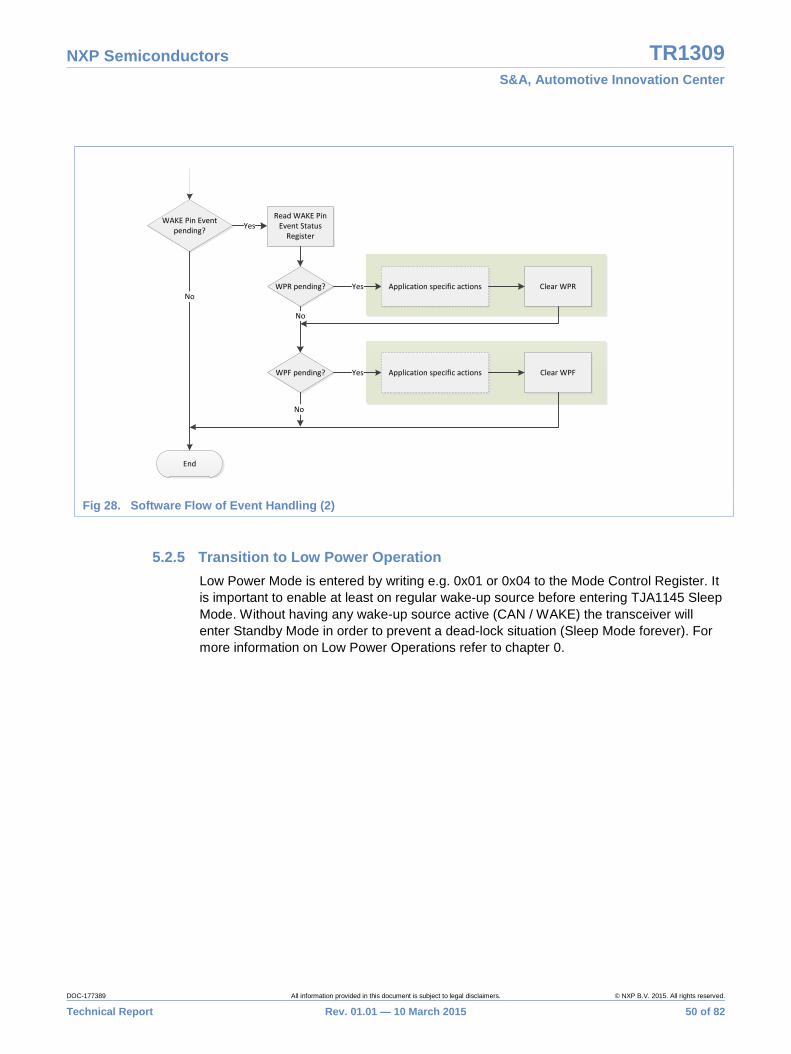
NXP Semiconductors TR1309 S&A, Automotive Innovation Center
DOC-177389 All information provided in this document is subject to legal disclaimers. © NXP B.V. 2015. All rights reserved.
Technical Report Rev. 01.01 — 10 March 2015 50 of 82
WAKE Pin Event pending?
Yes
End
No
Read WAKE Pin Event Status
Register
WPR pending?
WPF pending?
No
Clear WPRYes
Clear WPF Yes
No
Application specific actions
Application specific actions
Fig 28. Software Flow of Event Handling (2)
5.2.5 Transition to Low Power Operation
Low Power Mode is entered by writing e.g. 0x01 or 0x04 to the Mode Control Register. It
is important to enable at least on regular wake-up source before entering TJA1145 Sleep
Mode. Without having any wake-up source active (CAN / WAKE) the transceiver will
enter Standby Mode in order to prevent a dead-lock situation (Sleep Mode forever). For
more information on Low Power Operations refer to chapter 0.

NXP Semiconductors TR1309 S&A, Automotive Innovation Center
DOC-177389 All information provided in this document is subject to legal disclaimers. © NXP B.V. 2015. All rights reserved.
Technical Report Rev. 01.01 — 10 March 2015 51 of 82
5.3 Low Power Operation
This section introduces the software operations, which are associated to Low Power
Operation of the application. It is related to the Standby and Sleep Mode of TJA1145.
The difference between both modes is the amount of power that can be saved. In Sleep
Mode, there is the lowest current consumption but the delay between wake-up event and
restart of application is longer, because the system has to start from an un-powered
situation. In Standby Mode the current consumption is slightly higher compared to Sleep
mode with the benefit of a much shorter delay between wake-up event and re-start of
application. Therefore the following subchapters discuss the Standby and Sleep Mode in
more details.
As illustrated in Fig 29, Low Power Operation can be entered directly from Normal Mode
via SPI command. Moreover, Sleep Mode can also be entered via a temporary transition
to Standby Mode by using two consecutive SPI commands (1. enter Standby Mode, 2.
enter Sleep Mode). All mode transitions are performed by the dedicated SPI commands.
Standby
SleepNormal
SPI command
Wake-up
Power-on
SPI command
SPI command
SPI command
leaving Overtemp
VCC or VIO undervoltage
Fig 29. Simplified mode diagram with focus on Low Power Operation

NXP Semiconductors TR1309 S&A, Automotive Innovation Center
DOC-177389 All information provided in this document is subject to legal disclaimers. © NXP B.V. 2015. All rights reserved.
Technical Report Rev. 01.01 — 10 March 2015 52 of 82
5.3.1 Wake-Up Handling
The different events in the Event Status registers can be used as a wake-up event from
Low Power Operation. All events can be used as wake-up out of Low power (Standby
and Sleep Mode).
The TJA1145 Transceiver does not distinguish between wake-up and events. That
means that every enabled event source also causes a wake-up out of Low Power. So
after awaking out of Low Power Mode the RXD pin is forced low, as long as the event is
pending.
Power-onVBAT > 4.5V
Reset
Startup Operation(chapter 5.1)
Normal Operation(chapter 5.2)
Standby Mode requested?
Sleep Mode (chapter 5.3.2)
No
Stop Mode(chapter 5.3.3.1)
Yes
Wake-up
Wait for wake-up event
Wait for interrupt event
RXD Low Handling(chapter 5.3.1.1)
Preparation of In-Vehicle flashing
Low Power Operation Mode
(chapter 5.3)
In-Vehicle Flashing
In-Vehicle Flashing (chapter 5.3)
Fig 30. Event handling in Sleep and Standby Mode
In case of wake-up out of Sleep the “event handling” is performed by the Startup
operation because it is linked to a system reset event with powering up the application
(chapter 5.1). The only difference is the trigger event of the Startup Operation, which is a
wake-up event and not a power-on.

NXP Semiconductors TR1309 S&A, Automotive Innovation Center
DOC-177389 All information provided in this document is subject to legal disclaimers. © NXP B.V. 2015. All rights reserved.
Technical Report Rev. 01.01 — 10 March 2015 53 of 82
In case of wake-up out of Standby Mode the “event handling” is performed by the
interrupt service routine, triggered by the falling edge of the RXD pin. Hence, event
handling is called “RXD Low Handling” in this case. This functions differs slightly from the
Event Handling done after Startup or during Normal Operation because additional
actions are required for some events e.g. Enter Stop Mode again. Further information is
given in the following section.
5.3.1.1 RXD Low Handling
Error! Reference source not found. illustrates the software flow of the RXD Low
Handling. When any kind of event is pending in Standby Mode, the RXD pin is forced on
low level. The interrupt service can be implemented in the microcontroller with an CAN
Controller Wake-up interrupt that is triggered with a falling edge of the RXD pin or by
reading the Event Capture Status Register on a regular basis (polling).
The Event Capture Status Register gives a summary of all possible kinds of pending
events and allows getting an overview about event sources by only reading out one
register. After a read access to the Event Capture Status Register, the registers are
known where events are pending and which should be read out afterwards to identify the
pending event sources in detail.
After reading the detailed event registers (Transceiver Event Status Register, System
Event Status Register, Wake Pin Event Status Register) the read data are evaluated. If a
pending event is determined, the related service routine is called. The service routines
are application specific functions and depend on the need of the application. For
example, in case of the PNFDE event all registers related to Partial networking should be
reconfigured and checked.
Fig 31 and Fig 32 illustrate the software flow in case a RXD Low interrupt (CAN wake-up)
occurs.

NXP Semiconductors TR1309 S&A, Automotive Innovation Center
DOC-177389 All information provided in this document is subject to legal disclaimers. © NXP B.V. 2015. All rights reserved.
Technical Report Rev. 01.01 — 10 March 2015 54 of 82
Read Global Event Status Register
System Event pending?
No
Yes
Start Event Handling
Read System Event Status Register
OTW pending?
SPIF pending?
No
No
Application specific actions (e.g. store important data in NVM, store error in failure memory)
Clear OTWYes
Application specific actions (e.g. store error in failure memory)
Clear SPIFYes
Application specific
Associated Event Service Routine
Schedule change to Standby Operation
Schedule change to Standby Operation
Fig 31. Software flow of RXD Low Handler (1)

NXP Semiconductors TR1309 S&A, Automotive Innovation Center
DOC-177389 All information provided in this document is subject to legal disclaimers. © NXP B.V. 2015. All rights reserved.
Technical Report Rev. 01.01 — 10 March 2015 55 of 82
Transceiver Event pending?
No
WAKE Pin Event pending?
Yes
Yes
End
No
Read Transceiver Event Status
Register
CW pending?
CF pending?
No
No
CBS pending?
Clear CWYes
Application specific actions, e.g. start polling Transceiver Status (CFS, CTS, VCS); store
error in failure memory
Clear CFYes
Application specific actions Clear CBSYes
CAN wake-up actions, e.g. store wake-up reason (WUP
or WUF)
PNFDE pending?
No
Clear PNFDE
Application specific actions (e.g. store error in failure
memory, reconfigure partial networking registers)
Yes
No
Read WAKE Pin Event Status
Register
WPR pending?
WPF pending?
No
Clear WPRYes
Clear WPF Yes
No
Application specific actions
Application specific actions
Schedule change to Normal Operation
Schedule change to Standby Operation
Schedule change to Sleep
Operation
Schedule change to Normal Operation
Store Wake-up reason SYSERR
Schedule change to Normal Operation
Store Wake-up reason PIN
Schedule change to Normal Operation
Store Wake-up reason PIN
Fig 32. Software flow of RXD Low Handler (2)

NXP Semiconductors TR1309 S&A, Automotive Innovation Center
DOC-177389 All information provided in this document is subject to legal disclaimers. © NXP B.V. 2015. All rights reserved.
Technical Report Rev. 01.01 — 10 March 2015 56 of 82
5.3.2 Sleep Operation
Sleep Mode is a special kind of Low Power Operation. It can be entered from Standby
and Normal Mode via the 0x01 SPI command, which is a write access the Mode Control
Register. There are many possibilities to leave Sleep Mode and enter Standby Mode,
e.g. wake-up event on CAN or the WAKE pin or diagnosis events. It depends on the
events enabled when entering Sleep Mode.
After the wake-up event the Startup Operation is performed. For more information on
Startup Operations refer to chapter 5.1.
Standby
SleepNormal
SPI command
Wake-up
Power-on
SPI command
SPI command
SPI command
leaving Overtemp
VCC or VIO undervoltage
Fig 33. Simplified mode diagram with focus on Low Power Operation (Sleep Mode)
The software flow for entering Sleep Mode is shown in Fig 34.

NXP Semiconductors TR1309 S&A, Automotive Innovation Center
DOC-177389 All information provided in this document is subject to legal disclaimers. © NXP B.V. 2015. All rights reserved.
Technical Report Rev. 01.01 — 10 March 2015 57 of 82
Enter Sleep Operation Mode
Is Sleep Event / Wake-up configuration ok?
Yes
Event configuration for Sleep Mode
Is at least one regular wake-up enabled?
SBC enters Sleep Mode (SPI command = 0x0201)
Sleep Mode
Abort Sleep Mode transitionNo
Abort Sleep Mode transition: Schedule Event Handling & Change to
Normal Operation Mode
If SBC is in Normal Mode, stop CAN transmission
Configure Can Partial Networking Control
(CPNC)
Any event pending? Yes
Partial Networking enabled (CPNC == 1)?
No
Clear WUF flagEnter CAN PE Stop Mode;
wake-up disabled
Enter CAN PE Stop Mode; wake-up disabled
SBC enters Standby Mode (SPI command = 0x0204 )
Enter CAN PE Sleep Mode; wake-up enabled
Enter CAN PE Sleep Mode; wake-up enabled
SBC enters Standby Mode (SPI command = 0x0204 )
RXD low? Event pending? (Check WUF
flag)
No Yes
No Yes

NXP Semiconductors TR1309 S&A, Automotive Innovation Center
DOC-177389 All information provided in this document is subject to legal disclaimers. © NXP B.V. 2015. All rights reserved.
Technical Report Rev. 01.01 — 10 March 2015 58 of 82
Fig 34. Transition to Sleep Mode software flow
The first action during Sleep Mode preparation is to check if the required wake-up
sources will be enabled in Sleep Mode. Entering Sleep Mode without any active wake-up
source will end up into Standby Mode in order to prevent a possible dead-lock.
Therefore, at least one regular wake-up source must be enabled.
If the wake-up configuration in Sleep Mode is successfully checked, CAN communication
is stopped (if still enabled) and all wake-up sources for Sleep Mode are enabled by write
accesses to the related Event Enable Registers. For example, the 0x4601 SPI command
enables the CAN wake-up sources. Furthermore, the CAN Partial Networking Control
(CPNC) bit must be configured in the CAN Control Register.
When the wake-up sources and CPNC bit are configured properly, the software can
check if events are still pending. Therefore a read access to the Event Capture Status
Register is performed (SPI command: 0xC100). If an event is pending the TJA1145
cannot enter Sleep Mode and any attempt to enter Sleep Mode would lead to enter
Standby Mode. Therefore, the Sleep transition should be aborted (change to Normal
Operation and Event Handing). If no event is pending and CAN Partial Networking is
disabled, the CAN PE is put into Sleep Mode and afterwards the TJA1145 directly enters
Standby Mode, by a write access to the Mode Control Register (SPI command: 0x0204).
If no event is pending and CAN Partial Networking is enabled, a special shutdown
sequence is necessary in order not to lose any event:
1. The WUF flag in the transceiver is cleared.
2. The CAN PE is put into Stop Mode (wake-up disabled) in order not to wake-up
on any CAN communication, until the transceiver has entered Standby Mode.
3. Then transceiver is put into Standby Mode (SPI command = 0x0204)
4. The CAN PE is put into Sleep Mode (wake-up enabled) to allow signalling every
Transceiver event by a CAN wake-up interrupt.
5. As there might have occurred an event in between change of CAN PE from Stop
to Sleep Mode and RXD might clamp on low level (especially for edge sensitive
CAN Controller), e.g. due to CAN wake-up frame, a read access to the Event
Capture Status Register must be performed (SPI command: 0xC100). If an event
is pending, the Sleep transition should be aborted (Change to Normal Operation
and Event Handing).
Having successfully configured the CAN PE to Sleep Mode and the transceiver to
Standby Mode, the TJA1145 can enter Sleep Mode with a SPI write access (SPI
command: 0x0201) to the Mode Control Register.

NXP Semiconductors TR1309 S&A, Automotive Innovation Center
DOC-177389 All information provided in this document is subject to legal disclaimers. © NXP B.V. 2015. All rights reserved.
Technical Report Rev. 01.01 — 10 March 2015 59 of 82
5.3.3 Standby Operation
A different kind of Low Power Operation is the so called Stop or Sub Clock operation.
This operation is related to the Standby Mode of the TJA1145 because it requires a
supplied microcontroller. Stop or Sub Clock operation is a low power feature of the
microcontroller itself. Therefore, it will take place in Standby Mode of the TJA1145 and a
wake-up from Stop/Sub Clock operation will not lead to mode changes of the TJA1145.
Standby
SleepNormal
SPI command
Wake-up
Power-on
SPI command
SPI command
SPI command
leaving Overtemp
VCC or VIO undervoltage
Fig 35. Simplified mode diagram with focus on Low Power Operation (Standby Mode)
Stop or Sub clock operation can be realized by two different ways that are discussed
within the next subchapter. One part is the pure Stop operation and the other one is the
cyclic wake-up out of Stop operation.

NXP Semiconductors TR1309 S&A, Automotive Innovation Center
DOC-177389 All information provided in this document is subject to legal disclaimers. © NXP B.V. 2015. All rights reserved.
Technical Report Rev. 01.01 — 10 March 2015 60 of 82
5.3.3.1 Stop/Sub Clock operation
Fig 36 shows the required actions before entering Stop Mode. The first part of the Stop
Operation is to check if the necessary wake-ups will be enabled in Stop Mode. If the
wake-up configuration in Standby Mode or rather Stop Operation is successfully
checked, the CAN communication is stopped (if still enabled) and the wake-up sources
for Standby Mode are enabled by write accesses to the related Event Enable Registers.
For example, the 0x4601 SPI command enables the CAN wake-up source. Furthermore,
the CAN Partial Networking Control (CPNC) bit must be configured in the CAN Control
Register.
When the event sources and CPNC bit are configured properly the software can check if
events are still pending. This is done by a read access to the Event Capture Status
Register (SPI command: 0xC100). If an event is pending for safety reasons no Stop
Mode of the microcontroller and hence also no Transceiver Standby Mode is possible. As
consequence the transition to Stop Operation should be aborted (change to Normal
Operation and handle event).
If no event is pending, depending on the CPNC configuration the CAN PE is brought into
Sleep Mode and the TJA1145 is put into Standby Mode in a special sequence:
a. If CAN Partial Networking is disabled, the CAN PE is put into Sleep Mode and
afterwards the TJA1145 directly enters Standby Mode, by a write access to the
Mode Control Register (SPI command: 0x0204).
b. If CAN Partial Networking is enabled a special shutdown sequence is necessary in
order not to lose any event:
1. The WUF flag in the transceiver is cleared.
2. The CAN PE is put into Stop Mode (wake-up disabled) in order not to wake-up
on any CAN communication, until the transceiver has entered Standby Mode.
3. Then transceiver is put into Standby Mode (SPI command = 0x0204)
4. The CAN PE is put into Sleep Mode (wake-up enabled) to allow signalling every
Transceiver event by a CAN wake-up interrupt.
5. As there might have occurred an event in between change of CAN PE from Stop
to Sleep Mode and RXD might clamp on low level (especially for edge sensitive
CAN Controller), e.g. due to CAN wake-up frame, a read access to the Event
Capture Status Register must be performed (SPI command: 0xC100). If an event
is pending, the Sleep transition should be aborted (Change to Normal Operation
and Event Handing).
Having successfully configured the CAN PE to Sleep Mode and the transceiver to
Standby Mode, the Stop/Sub Clock operation of the microcontroller can be entered by
disabling the oscillator completely or switching to a lower clock frequency.

NXP Semiconductors TR1309 S&A, Automotive Innovation Center
DOC-177389 All information provided in this document is subject to legal disclaimers. © NXP B.V. 2015. All rights reserved.
Technical Report Rev. 01.01 — 10 March 2015 61 of 82
Enter Stop Operation Mode
Is Standby Event /wake-up
configuration ok?
Yes
Event configuration for Standby Mode
Disable MCU Oscillator
Abort Standby Mode transition
No
Abort Stop Mode transition: Schedule Event Handling & Change to
Normal Operation Mode
If SBC is in Normal Mode, stop CAN transmission
Configure CAN Partial Networking Control
(CPNC)Any event pending? Yes
Partial Networking enabled (CPNC == 1)?
No
Clear WUF flagEnter CAN PE Stop Mode;
wake-up disabled
Enter CAN PE Stop Mode; wake-up disabled
SBC enters Standby Mode (SPI command = 0x0204 )
Enter CAN PE Sleep Mode; wake-up enabled
Enter CAN PE Sleep Mode; wake-up enabled
SBC enters Standby Mode (SPI command = 0x0204 )
Any TJA1145 Event pending?
(Check WUF flag)
No Yes
No Yes
Stop Mode
Is RXD pin high?
Yes
No

NXP Semiconductors TR1309 S&A, Automotive Innovation Center
DOC-177389 All information provided in this document is subject to legal disclaimers. © NXP B.V. 2015. All rights reserved.
Technical Report Rev. 01.01 — 10 March 2015 62 of 82
Fig 36. Transition to Stop Mode software flow
5.4 In-Vehicle Flash Operation
This chapter will not explain the H.I.S Standard and how to flash a device within a
vehicle. It will only give a very short overview of the SW flow of the In-Vehicle Flash
process.
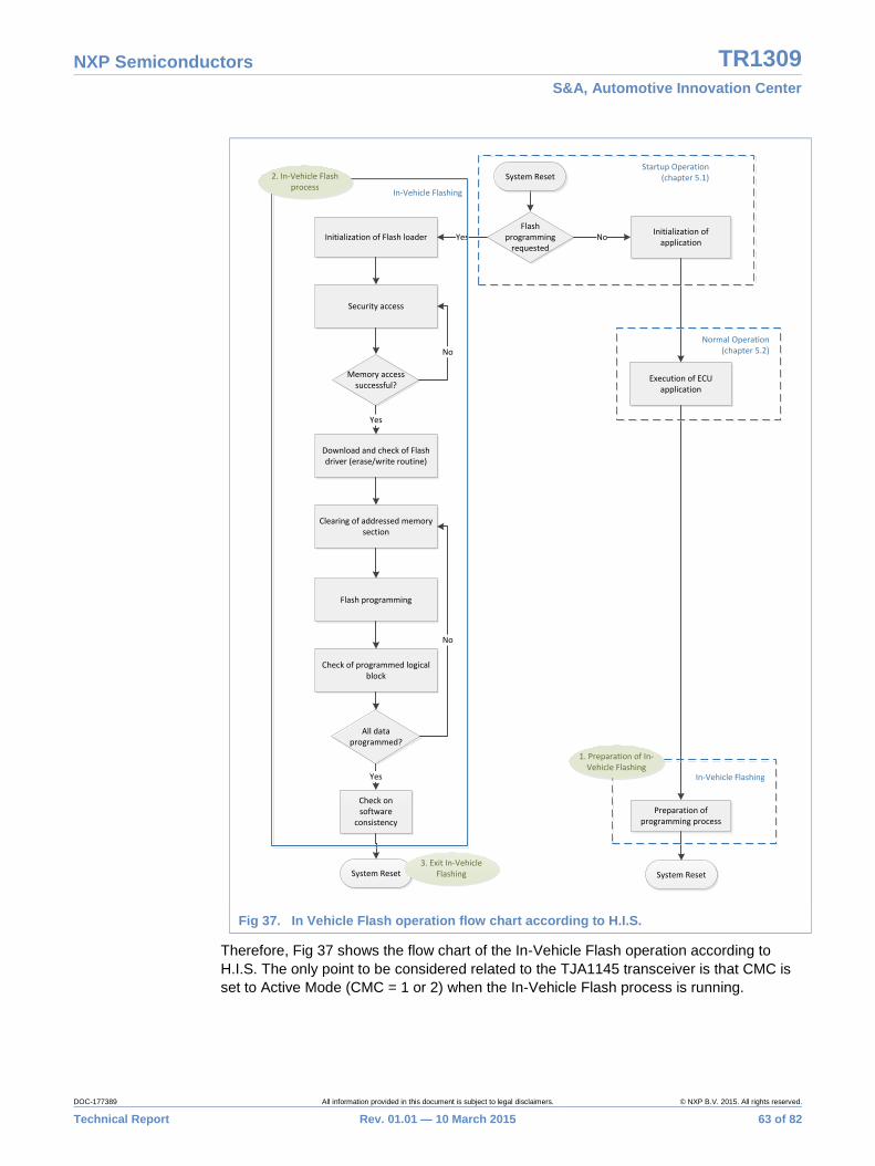
NXP Semiconductors TR1309 S&A, Automotive Innovation Center
DOC-177389 All information provided in this document is subject to legal disclaimers. © NXP B.V. 2015. All rights reserved.
Technical Report Rev. 01.01 — 10 March 2015 63 of 82
Flash programming
requestedInitialization of Flash loader
Initialization of application
Memory access successful?
Yes No
System Reset
System Reset
Execution of ECU application
Preparation of programming process
Security access
No
Download and check of Flash driver (erase/write routine)
Yes
Clearing of addressed memory section
Flash programming
Check of programmed logical block
All data programmed?
Check on software
consistency
Yes
System Reset
No
Startup Operation (chapter 5.1)
In-Vehicle Flashing
Normal Operation(chapter 5.2)
In-Vehicle Flashing
1. Preparation of In-Vehicle Flashing
2. In-Vehicle Flash process
3. Exit In-Vehicle Flashing
Fig 37. In Vehicle Flash operation flow chart according to H.I.S.
Therefore, Fig 37 shows the flow chart of the In-Vehicle Flash operation according to
H.I.S. The only point to be considered related to the TJA1145 transceiver is that CMC is
set to Active Mode (CMC = 1 or 2) when the In-Vehicle Flash process is running.

NXP Semiconductors TR1309 S&A, Automotive Innovation Center
DOC-177389 All information provided in this document is subject to legal disclaimers. © NXP B.V. 2015. All rights reserved.
Technical Report Rev. 01.01 — 10 March 2015 64 of 82
6. Appendix
6.1 Printed Circuit board design rules
Following rules should be considered for the PCB layout:
The TJA1145 with the ending -TK are delivered in a HVSON14 package with an
exposed die pad. In order to enhance thermal and electrical performance, it is
recommended to also solder the exposed center pad to board GND.
Additional PCB layout options improve the thermal resistance:
o Number of PCB layers (the more the better)
o Cu thickness (35μm/70μm; the thicker the better)
o Heat sink area on the PCB available for the TJA1145 (the bigger the
better)
o Number of vias (the more the better)
o An increase of the heat sink area on the top layer is more efficient than
an extension of the heat sink on the bottom layers. Hence, for a good
thermal performance of the PCB it is recommended to exploit as much
area on the top layer as heat sink as possible and use the other layers
for further optimization.
When a common mode choke is used, it should be placed close to the bus pins
CANH and CANL.
The PCB tracks for the bus signals CANH and CANL should be routed close
together in a symmetrical way. Its length should not exceed ~10cm.
Avoid routing other “off-board” signal lines parallel to the CANH/CANL lines on
the PCB due to potential “single ended” noise injection into CAN wires.
In case further ESD protection is required it should be connected close to the
ECU connector bus terminals.
The track length between communication controller / μC and the TJA1145 should
be as short as possible.
The ground impedance between communication controller (μC) and TJA1145
should be as low as possible.
Avoid applying filter elements into the GND signal of the μC or the TJA1145.
GND has to be the same for the TJA1145 and μC.

NXP Semiconductors TR1309 S&A, Automotive Innovation Center
DOC-177389 All information provided in this document is subject to legal disclaimers. © NXP B.V. 2015. All rights reserved.
Technical Report Rev. 01.01 — 10 March 2015 65 of 82
6.2 Pin FMEA
This chapter provides an FMEA (Failure Mode and Effect Analysis) for typical failure
situations, when dedicated pins of the TJA1145 are short-circuited to supply voltages like
BAT, VCC, GND or neighbored pins or simply left open. The individual failures are
classified, due to their corresponding effect on the transceiver, the application and the
bus communication. Following classes of severity are distinguished:
Table 4. Classification of severity of effects
Severity Class Effects
A - Damage to device
- Serial communication on CAN may be affected globally
B
- No damage to device
- Serial communication in the overall system not possible (global
problem)
C
- No damage to device
- Bus communication of other nodes in the system possible
- Corrupted node not able to communicate (local problem)
- Application might shut-down
D
- No damage to device
- Bus communication in the overall system possible
- Reduced functionality of application
- - Not affected at all

NXP Semiconductors TR1309 S&A, Automotive Innovation Center
DOC-177389 All information provided in this document is subject to legal disclaimers. © NXP B.V. 2015. All rights reserved.
Technical Report Rev. 01.01 — 10 March 2015 66 of 82
Table 5. Pin FMEA for TJA1145 and TJA1145/FD
Pin Name Failure Remark Severity
Class
Pin 1:
TXD
Shorted to neighbor (GND) TRX detects this short and disables the CAN transmitter;
no effects on other nodes. Consider functionality of
connected MCU pin.
C
Shorted to VCC No transmission of CAN messages possible; node runs
bus off; no effect on the communication of the other
nodes; reception still possible. Consider functionality of
connected MCU pin.
D
Shorted to BAT (>6V) TRX damaged by exceeding limiting value of pin TXD. A
Open Circuit No transmission of CAN frames possible; CAN controller
runs bus off; no effect on other nodes communication;
reception still possible.
D
Pin 2:
GND
Shorted to neighbor (VCC) VCC under voltage detection; TRX enters Sleep Mode. C
Shorted to BAT Fundamental problem of ECU; no supply available; TRX
not affected.
Shorted to GND Normal Operation -
Open Circuit Fundamental problem of ECU; no supply available; TRX
and components on ECU might become damaged. (A)
Pin 3:
VCC
Shorted to neighbor (RXD) Short-term disturbance of CAN communication until
CAN error counter reaches limit and CAN protocol
engine stops CAN transmission; bus is off; other nodes
not affected
C
Shorted to VCC Normal Operation -
Shorted to BAT (>6V) TRX damaged by exceeding limiting value of pin VCC. A
Shorted to GND VCC under voltage detection; TRX enters Sleep Mode. C
Open Circuit VCC under voltage detection; TRX enters Sleep Mode. C
Pin 4:
RXD
Shorted to neighbor (VIO) RXD clamped recessive; Short-term disturbance of CAN
communication until CAN error counter reaches limit and
CAN protocol engine stops CAN transmission; bus is off;
other nodes not affected
C

NXP Semiconductors TR1309 S&A, Automotive Innovation Center
DOC-177389 All information provided in this document is subject to legal disclaimers. © NXP B.V. 2015. All rights reserved.
Technical Report Rev. 01.01 — 10 March 2015 67 of 82
Pin Name Failure Remark Severity
Class
Shorted to VCC RXD clamped recessive; Short-term disturbance of CAN
communication until CAN error counter reaches limit and
CAN protocol engine stops CAN transmission; bus Is off;
other nodes not affected.
Consider functionality of connected MCU pin.
C
Shorted to BAT (>6V) TRX damaged by exceeding limiting value of pin RXD. A
Shorted to GND Short-term disturbance of CAN communication until
CAN error counter reaches limit and CAN protocol
engine stops CAN transmission; bus is off; other nodes
not affected
C
Open Circuit Short-term disturbance of CAN communication until
CAN error counter reaches limit and CAN protocol
engine stops CAN transmission; bus is off; other nodes
not affected
C
Pin 5:
VIO
Shorted to neighbor (SDO) Cannot read from TRX; behavior depends on software. C / D
Shorted to VCC Consider functionality of connected MCU pin. C
Shorted to BAT (>6V) TRX damaged by exceeding limiting value of pin VIO. A
Shorted to GND VIO under voltage detection; TRX enters Sleep Mode. C
Open Circuit VIO under voltage detection; TRX enters Sleep Mode. C
Pin 6:
SDO
Shorted to neighbor (INH) TRX damaged by exceeding limiting value of pin SDO
by INH = BAT level. A
Shorted to VCC Cannot read from TRX; behavior depends on software.
Consider functionality of connected MCU pin. C / D
Shorted to BAT (>6V) TRX damaged by exceeding limiting value of pin SDO. A
Shorted to GND Cannot read from TRX; behavior depends on software. C / D
Open Circuit Cannot read from TRX; behavior depends on software. C / D
Pin 7:
INH
Shorted to VCC TRX damaged by exceeding limiting value of pin VCC
by INH = BAT level. A
Shorted to BAT INH controlled components keep permanently on. D

NXP Semiconductors TR1309 S&A, Automotive Innovation Center
DOC-177389 All information provided in this document is subject to legal disclaimers. © NXP B.V. 2015. All rights reserved.
Technical Report Rev. 01.01 — 10 March 2015 68 of 82
Pin Name Failure Remark Severity
Class
Shorted to GND INH controlled components keep permanently off. C
Open Circuit INH controlled components keep permanently off. C
Pin 8:
SCK
Shorted to neighbor (WAKE) In case of WAKE pin input voltage related to BAT supply
TRX damaged by exceeding limiting value of pin SCK.
In case of WAKE pin input voltage related to SCK
limiting value range no communication towards TRX.
Consider functionality of connected MCU pin.
A
C
Shorted to VCC No communication towards TRX. Consider functionality
of connected MCU pin. C
Shorted to BAT (>6V) TRX damaged by exceeding limiting value of pin SCK. A
Shorted to GND No communication towards TRX. Consider functionality
of connected MCU pin. C
Open Circuit No communication towards TRX. C
Pin 9:
WAKE
Shorted to neighbor (BAT) No local wake-up possible D
Shorted to VCC In case of WAKE pin input voltage related to BAT supply
TRX damaged by exceeding limiting value of pin VCC.
In case of WAKE pin input voltage related to VCC
limiting value range a LOW input level on pin WAKE
cause a VVC under voltage detection. TRX enters Sleep
Mode.
A
C
Shorted to GND No local wake-up possible D
Open Circuit No local wake-up possible D
Pin 10:
BAT
Shorted to neighbor (SDI) In case of BAT>6V TRX damaged by exceeding limiting
value of pin SDI. A
Shorted to VCC In case of BAT>6V TRX damaged by exceeding limiting
value of pin VCC. A
Shorted to BAT Normal operation -
Shorted to GND Fundamental problem of ECU; no supply available; TRX
not affected

NXP Semiconductors TR1309 S&A, Automotive Innovation Center
DOC-177389 All information provided in this document is subject to legal disclaimers. © NXP B.V. 2015. All rights reserved.
Technical Report Rev. 01.01 — 10 March 2015 69 of 82
Open Circuit TRX not supplied; behaves passive to the bus. C
Pin 11:
SDI
Shorted to neighbor (CANL) No communication towards TRX. Consider functionality
of connected MCU pin. In case of CANL peak >6V TRX
damaged by exceeding limiting value of pin SDI. Serial
communication on CAN may be affected globally.
A
Shorted to VCC No communication towards TRX. Consider functionality
of connected MCU pin. C
Shorted to BAT In case of BAT>6V TRX damaged by exceeding limiting
value of pin SDI. C
Shorted to GND No communication towards TRX. Consider functionality
of connected MCU pin. C
Open Circuit No communication towards TRX. C
Pin 12:
CANL
Shorted to neighbor (CANH) No communication possible (no differential signal) B
Shorted to VCC No communication possible (no differential signal) B
Shorted to BAT No communication possible (no differential signal) B
Shorted to GND Communication still possible (differential signal still
available; CANH recessive level lowered to GND level) D
Open Circuit No communication possible (no differential signal) B
Pin 13:
CANH
Shorted to neighbor (SCSN) No communication towards TRX. Consider functionality
of connected MCU pin.
In case of CANH peak >6V TRX damaged by exceeding
limiting value of pin SCSN.
Serial communication on CAN may be affected globally.
A
Shorted to VCC Communication still possible (differential signal still
available; CANH recessive level increased to VCC
level)
D
Shorted to BAT Communication still possible (differential signal still
available; CANH recessive level increased to BAT level) D
Shorted to GND No communication possible (no differential signal) B
Open Circuit No communication possible (no differential signal) B
Pin 14: Shorted to VCC No communication towards TRX. Consider functionality
of connected MCU pin. C

NXP Semiconductors TR1309 S&A, Automotive Innovation Center
DOC-177389 All information provided in this document is subject to legal disclaimers. © NXP B.V. 2015. All rights reserved.
Technical Report Rev. 01.01 — 10 March 2015 70 of 82
SCSN Shorted to BAT (>6V) TRX damaged by exceeding limiting value of pin SCSN. A
Shorted to GND No communication towards TRX. Consider functionality
of connected MCU pin. C
Open Circuit No communication towards TRX. C

NXP Semiconductors TR1309 S&A, Automotive Innovation Center
DOC-177389 All information provided in this document is subject to legal disclaimers. © NXP B.V. 2015. All rights reserved.
Technical Report Rev. 01.01 — 10 March 2015 71 of 82
6.3 Attached Files
Attached to these application hints you can find source code for a TJA1145/FD
Transceiver example project and its software documentation. Table 6 specifies the
attachments and gives an overview and a detailed description of the files.
Table 6. Attached Files
Attached File Description
TJA1145FD_ApplHint.c C-file containing the main function
NXP_TJA1145FD_Functions.c Header file for TJA1145/FD/VX Transceiver
low level driver
NXP_TJA1145FD_Functions.h C-file implementing TJA1145/FD/VX
Transceiver low level driver
NXP_TJA1145FD_Sim.h Header file containing typedefs for the
TJA1145/FD/VX Transceiver registers
NXP_UJA11XX_defines.h Header file defining data types and general
typedefs
TJA1145FD_Application_Specific_Functions.h Header file defining application specific
functions
TJA1145FD_Application_Specific_Functions.c C-file implementing application specific
functions
uC_Specific_Functions.h Header file defining microcontroller specific
functions
uC_Specific_Function.c C-file containing microcontroller specific
functions that must be implemented by the
SW designer
TJA1145FD_Configuration.h Header file containing the application
configuration of the TJA1145/FD/VX
Transceiver in different operating modes
TJA1145FD_Appl_Hints_Software_Documentation.
zip.txt
Documentation of the example project;
Please remove the suffix “.txt” and extract
the ZIP-archive afterwards.

NXP Semiconductors TR1309 S&A, Automotive Innovation Center
DOC-177389
© NXP B.V. 2015. All rights reserved.
Technical Report Rev. 01.01 — 10 March 2015 72 of 82
6.4 NXPs self supplied high speed CAN transceiver
6.4.1 UJA1161 – Self supplied high CAN transceiver with Standby Mode
UJA1161 – Self supplied high speed CAN transceiver with Standby Mode
1
UJA11614
3
2
5
6
14
11
12
13
10
9
7 8
TXD
GND
BUF
RXD
VIO
CTS
n.c.
STBN
CANH
CANL
n.c.
BAT
n.c.
n.c.
- Self-supplied high-speed CAN transceiver
- ISO 11898-5 compliant
- Autonomous bus biasing according to ISO 11898-6
- Fully integrated 5 V supply (BUF) for CAN transmitter/receiver
- VIO allows for direct interfacing with 3.3 V to 5 V microcontrollers
- Standby mode featuring very low supply current
- Remote wake-up capability
Fig 38. Pin configuration and short functional description of the UJA1161
6.4.2 UJA1162 – Self supplied high CAN transceiver with Sleep Mode
UJA1162 – Self supplied high speed CAN transceiver with Sleep Mode
1
UJA11624
3
2
5
6
14
11
12
13
10
9
7 8
TXD
GND
BUF
RXD
VIO
CTS
INH
SLPN
CANH
CANL
n.c.
BAT
WAKE
n.c.
- Self-supplied high-speed CAN transceiver
- ISO 11898-5 compliant
- Autonomous bus biasing according to ISO 11898-6
- Fully integrated 5 V supply (BUF) for CAN transmitter/receiver
- VIO allows for direct interfacing with 3.3 V to 5 V microcontrollers
- Sleep mode featuring very low supply current (BUF off)
- Remote wake-up capability
- Local wake-up capability via the WAKE pin
- Entire node can be powered down via the inhibit output, INH
Fig 39. Pin configuration and short functional description of the UJA1162

NXP Semiconductors TR1309 S&A, Automotive Innovation Center
DOC-177389
© NXP B.V. 2015. All rights reserved.
Technical Report Rev. 01.01 — 10 March 2015 73 of 82
6.5 NXPs mini high speed CAN SBC family
6.5.1 UJA1163 – Mini HSCAN SBC with Standby Mode w/o watchdog
UJA1163 – Mini HSCAN SBC with Standby Mode w/o watchdog
1
UJA11634
3
2
5
6
14
11
12
13
10
9
7 8
TXD
GND
V1
RXD
RSTN
CTS
n.c.
STBN
CANH
CANL
n.c.
BAT
n.c.
n.c.
- ISO 11898-5 compliant high-speed CAN transceiver
- Autonomous bus biasing according to ISO 11898-6
- Fully integrated 5 V/100 mA microcontroller supply (V1)
- Standby mode featuring very low supply current (V1 on)
- Remote wake-up capability
Fig 40. Pin configuration and short functional description of the UJA1163
6.5.2 UJA1164 – Mini HSCAN SBC with Standby Mode
UJA1164 – Mini HSCAN SBC with Standby Mode
1
UJA11644
3
2
5
6
14
11
12
13
10
9
7 8
TXD
GND
V1
RXD
RSTN
SDO
n.c.
SCSN
CANH
CANL
SDI
BAT
n.c.
SCK
- ISO 11898-5 compliant high-speed CAN transceiver
- Autonomous bus biasing according to ISO 11898-6
- Fully integrated 5 V/100 mA microcontroller supply (V1)
- Standby mode featuring very low supply current (V1 on)
- Remote wake-up capability
- Mode control via the Serial Peripheral Interface (SPI)
- Watchdog with independent clock source
- Configuration of selected functions via non-volatile memory
Fig 41. Pin configuration and short functional description of the UJA1164

NXP Semiconductors TR1309 S&A, Automotive Innovation Center
DOC-177389
© NXP B.V. 2015. All rights reserved.
Technical Report Rev. 01.01 — 10 March 2015 74 of 82
6.5.3 UJA1167 – Mini HSCAN SBC with Sleep Mode
UJA1167 – Mini HSCAN SBC with Sleep Mode
1
UJA11674
3
2
5
6
14
11
12
13
10
9
7 8
TXD
GND
V1
RXD
RSTN
SDO
INH/
VEXT
SCSN
CANH
CANL
SDI
BAT
WAKE
SCK
- ISO 11898-5 compliant high-speed CAN transceiver
- Autonomous bus biasing according to ISO 11898-6
- Fully integrated 5 V/100 mA microcontroller supply (V1)
- Standby & Sleep (V1 off) mode featuring very low supply current
- Remote and local wake-up capability
- INH output for controlling an external voltage regulator
- Optional 5V sensor supply voltage regulator
- Mode control via the Serial Peripheral Interface (SPI)
- Watchdog with independent clock source
- Configuration of selected functions via non-volatile memory
Fig 42. Pin configuration and short functional description of the UJA1167
6.5.4 UJA1168 – Mini HSCAN SBC for Partial Networking
UJA1163 – Mini HSCAN SBC for Partial Networking
1
UJA11684
3
2
5
6
14
11
12
13
10
9
7 8
TXD
GND
V1
RXD
RSTN
SDO
INH/
VEXT
SCSN
CANH
CANL
SDI
BAT
WAKE
SCK
- ISO 11898-6 compliant HSCAN for Partial Networking
- Autonomous bus biasing according to ISO 11898-6
- Fully integrated 5 V/100 mA microcontroller supply (V1)
- Standby & Sleep (V1 off) mode featuring very low supply current
- Remote and local wake-up capability
- INH output for controlling an external voltage regulator
- Optional 5V sensor supply voltage regulator
- Mode control via the Serial Peripheral Interface (SPI)
- Watchdog with independent clock source
- Configuration of selected functions via non-volatile memory
- CAN FD passive variant
Fig 43. Pin configuration and short functional description of the UJA1168

NXP Semiconductors TR1309 S&A, Automotive Innovation Center
DOC-177389
© NXP B.V. 2015. All rights reserved.
Technical Report Rev. 01.01 — 10 March 2015 75 of 82
6.6 NXPs standalone high speed CAN transceiver products
6.6.1 TJA1051 – Basic high speed CAN transceiver
TJA1051 – Basic high speed CAN transceiver
TXD 8
7
6
5
1
2
3
4
GND
VCC
RXD
S
CANH
CANL
TJA1051
n.c.
- Successor of the TJA1050 basic high speed CAN transceiver
- Normal Mode (transmit / receive CAN data)
- Silent Mode (receiving CAN data only)
- Under voltage detection on pin VCC
TJA1051/3 – Basic high speed CAN transceiver with 3V microcontroller interface
TXD 8
7
6
5
1
2
3
4
GND
VCC
RXD
S
CANH
CANL
TJA1051/3
VIO
- Variant of the TJA1051 basic high speed CAN transceiver
including:
- Direct interfacing to microcontrollers with 3V to 5V supply voltage
- Under voltage detection on pin VIO
TJA1051/E – Basic high speed CAN transceiver with Off Mode
TXD 8
7
6
5
1
2
3
4
GND
VCC
RXD
S
CANH
CANL
TJA1051/E
EN
- Variant of the TJA1051 basic high speed CAN transceiver
including:
- Off Mode (disabled transceiver with zero bus load)
Fig 44. Pin configuration and short functional description of the TJA1051, TJA1051/3 and TJA1051/E

NXP Semiconductors TR1309 S&A, Automotive Innovation Center
DOC-177389
© NXP B.V. 2015. All rights reserved.
Technical Report Rev. 01.01 — 10 March 2015 76 of 82
6.6.2 TJA1042 – High speed CAN transceiver with Standby Mode
TJA1042 – High speed CAN transceiver with Standby Mode
TXD 8
7
6
5
1
2
3
4
GND
VCC
RXD
STB
CANH
CANL
TJA1042
SPLIT
- Successor of the TJA1040 high speed CAN transceiver
- Normal Mode (transmit / receive CAN data)
- Standby Mode (low power mode with CAN wake-up capability)
- SPLIT pin for recessive bus level stabilization
- Bus dominant time-out function in Standby Mode
- Undervoltage detection on pin VCC
TJA1042/3 – High speed CAN transceiver with Standby Mode and 3V microcontroller interface
TXD 8
7
6
5
1
2
3
4
GND
VCC
RXD
STB
CANH
CANL
TJA1042/3
VIO
- Variant of the TJA1042 high speed CAN transceiver
including:
- Direct interfacing to microcontrollers with 3V to 5V supply voltage
- Low power receiver supply in Standby Mode by VIO only
- Undervoltage detection on pin VIO
- No SPLIT pin for recessive bus level stabilization
Fig 45. Pin configuration and short functional description of the TJA1042 and TJA1042/3
6.6.3 TJA1048 – Dual high speed CAN transceiver with Standby Mode
TJA1048 – Dual high speed CAN transceiver with Standby Mode
TXD1 14
13
12
11
1
2
3
4
GNDA
VCC
RXD1
STBN1
CANH1
CANL1
TJA1048
5
6
7
10
9
8
GNDB
TXD2
RXD2
VIO
CANH2
CANL2
STBN2
- Dual CAN transceiver based on TJA1042/3
- Normal Mode (transmit / receive CAN data)
- Standby Mode (low power mode with CAN wake-up capability)
- Channel independent mode control
- Direct interfacing to microcontrollers with 3V to 5V supply voltage
- Low power receiver supply in Standby Mode by VIO only
- Under voltage detection on pins VCC and VIO
- Enhanced CAN wake-up pattern
Fig 46. Pin configuration and short functional description of the TJA1048

NXP Semiconductors TR1309 S&A, Automotive Innovation Center
DOC-177389
© NXP B.V. 2015. All rights reserved.
Technical Report Rev. 01.01 — 10 March 2015 77 of 82
6.6.4 TJA1043 – High speed CAN transceiver with Sleep Mode and diagnostics
TJA1043 – High speed CAN transceiver with Sleep Mode and diagnostics
TXD 14
13
12
11
1
2
3
4
GND
VCC
RXD
STBN
CANH
CANL
TJA1043 SPLIT
5
6
7
10
9
8
VIO
EN
INH
VBAT
WAKE
ERRN
- Successor of the TJA1041A high speed CAN transceiver
- Normal Mode (transmit / receive CAN data)
- Listen-only Mode (receiving CAN data only)
- Standby Mode (first-level low power mode – INH on)
- Sleep Mode (second-level low power mode – INH off)
- Local and remote wake-up with wake-up source recognition
- Direct interfacing to microcontrollers with 3V to 5V supply voltage
- SPLIT pin for recessive bus level stabilization
- Under voltage detection on pins VBAT, VCC and VIO
- Several protection and diagnostic functions
Fig 47. Pin configuration and short functional description of the TJA1043
6.6.5 TJA1044 / TJA1057 – Optimized high speed CAN transceiver; MANTISTM
TJA1057 / TJA1057/GT – Optimized high speed CAN transceiver
TXD 8
7
6
5
1
2
3
4
GND
VCC
RXD
S
CANH
CANL
TJA1057
TJA1057/GT
n.c.
- Optimized successor of the TJA1051 for 12V applications
- Suitable for choke less operation
- Logic levels compatible with 3.3 V and 5 V microcontrollers
- Dual sourced
- GT-version: EMC compliant up to 2 Mbps (with choke)
TJA1044 / TJA1044/GT – Optimized high speed CAN transceiver with Standby Mode
TXD 8
7
6
5
1
2
3
4
GND
VCC
RXD
STB
CANH
CANL
TJA1044
TJA1044/GT
n.c.
- Optimized successor of the TJA1052 for 12V applications
- Suitable for choke less operation
- Removal of the SPLIT pin (not required for modern networks)
- Logic levels compatible with 3.3 V and 5 V microcontrollers
- Dual sourced
- GT-version: EMC compliant up to 2 Mbps (with choke)
Fig 48. Pin configuration and short functional description of the TJA1057 and TJA1044

NXP Semiconductors TR1309 S&A, Automotive Innovation Center
DOC-177389
© NXP B.V. 2015. All rights reserved.
Technical Report Rev. 01.01 — 10 March 2015 78 of 82
6.7 NXPs integrated high speed CAN transceiver products
6.7.1 UJA107xA – Core System Basis Chip with integrated high speed CAN
UJA107xA – Core System Basis Chip with integrated high speed CAN transceiver
TXDL2 32
31
30
29
1
2
3
4
RXDL2
TXDL1
V1
BAT
VEXCTRL
TEST2
UJA107x
5
6
7
28
27
26
RXDL1
RSTN
INTN
VEXCC
WBIAS
LIN2
DLIN
8
9
10
11
12
13
14
15
16
25
24
23
22
21
20
19
18
17
EN
SDI
SDO
SCK
SCSN
TXDC
RXDC
TEST1
WDOFF
LIN1
SPLIT
GND
CANL
CANH
V2
WAKE2
WAKE1
LIMP
The core System Basis Chip (SBC) family replaces basis discrete components commonly found in ECUs:
- Advanced independent watchdog
- 250mA voltage regulator (150mA internal, scalable with PNP)
- Integrated voltage regulator for CAN
- Serial peripheral interface (SPI)
- 2 local wake-up input ports
- Limp home output port
- Advanced low-power concept
- Safe and controlled system start-up behavior
- Detailed status reporting on system and sub-system levels
High speed CAN variants:
- UJA1075A / High speed CAN / LIN core SBC
- UJA1076A / High speed CAN core SBC
- UJA1078A / High speed CAN / dual LIN core SBC
Fig 49. Pin configuration and short functional description of the UJA107xA

NXP Semiconductors TR1309 S&A, Automotive Innovation Center
DOC-177389
© NXP B.V. 2015. All rights reserved.
Technical Report Rev. 01.01 — 10 March 2015 79 of 82
6.7.2 UJA106x – Fail-safe System Basis Chip with integrated high speed CAN
UJA106x – Fail-safe System Basis Chip with integrated high speed CAN transceiver
n.c. 32
31
30
29
1
2
3
4
n.c.
TXDL
V1
BAT42
SENSE
V3
UJA106x
5
6
7
28
27
26
RXDL
RSTN
INTN
SYSINH
n.c.
BAT14
RTLIN
8
9
10
11
12
13
14
15
16
25
24
23
22
21
20
19
18
17
EN
SDI
SDO
SCK
SCS
TXDC
RXDC
n.c.
TEST
LIN
SPLIT
GND
CANL
CANH
V2
n.c.
WAKE
INH /
LIMP
The fail-safe System Basis Chip (SBC) family replaces basis discrete components commonly found in ECUs:
- Advanced independent watchdog
- Voltage regulators for microcontroller and CAN transceiver
- Serial peripheral interface (SPI)
- Local wake-up input port
- Inhibit/Limp home output port
- Advanced low-power concept
- Safe and controlled system start-up behavior
- Advanced fail-safe system behavior that prevents any deadlock
- Detailed status reporting on system and sub-system levels
High speed CAN variants:
- UJA1065 / High speed CAN / LIN fail-safe SBC
- UJA1066 / High speed CAN fail-safe SBC
Fig 50. Pin configuration and short functional description of the UJA106x

NXP Semiconductors TR1309 S&A, Automotive Innovation Center
DOC-177389
© NXP B.V. 2015. All rights reserved.
Technical Report Rev. 01.01 — 10 March 2015 80 of 82
7. Abbreviations
Table 1. Abbreviations
Acronym Description
CAN Controller Area Network
ECU Electronic Control Unit
EMC Electromagnetic Compatibility
EME Electromagnetic Emission
EMI Electromagnetic Immunity
ESD Electrostatic Discharge
FMEA Failure Mode and Effects Analysis
OEM Original Equipment Manufacturer
PE Protocol Engine
PCB Printed Circuit Board
SBC System Basis Chip
SPI Serial Peripheral Interface

NXP Semiconductors TR1309 S&A, Automotive Innovation Center
DOC-177389
© NXP B.V. 2015. All rights reserved.
Technical Report Rev. 01.01 — 10 March 2015 81 of 82
8. References
[1] Objective datasheet UJA1161, Self-supplied high-speed CAN transceiver with
Standby Mode – NXP Semiconductors, Rev. 00.04, 31 August 2012
[2] Objective datasheet UJA1162, Self-supplied high-speed CAN transceiver with
Sleep Mode – NXP Semiconductors, Rev. 00.06, 31 August 2012
[3] Objective datasheet UJA1163, Mini high-speed CAN system basis chip with
Standby Mode – NXP Semiconductors, Rev. 00.03, 3 May 2013
[4] Product datasheet UJA1164, Mini high-speed CAN system basis chip with Standby
Mode & Watchdog – NXP Semiconductors, Rev. 1.00, 5 August 2013
[5] Product datasheet UJA1167, Mini high-speed CAN system basis chip with Standby
/ Sleep Mode & Watchdog – NXP Semiconductors, Rev. 1.00, 5 August 2013
[6] Product datasheet UJA1168, Mini high-speed CAN system basis chip for partial
networking – NXP Semiconductors, Rev. 1.00, 5 August 2013
[7] Objective datasheet TJA1145, High-speed CAN transceiver for partial networking –
NXP Semiconductors, Rev. 00.15, 28 January 2013
[8] Application Hints, Rules and recommendations for in-vehicle CAN networks,
TR1135 – NXP Semiconductors, Rev. 00.01, 24 September 2012
[9] Application Hints, Partial Networking, AH1203 – NXP Semiconductors, Rev. 01.00,
22 February 2013

NXP Semiconductors TR1309 S&A, Automotive Innovation Center
Please be aware that important notices concerning this document and the product(s) described herein, have been included in the section 'Legal information'.
© NXP B.V. 2015. All rights reserved.
For more information, please visit: http://www.nxp.com
For sales office addresses, email to: [email protected]
Date of release: 10 March 2015
Document identifier: DOC-177389