Embed Size (px)
Citation preview
Technical University of GdañskDepartment of Medical and Ecological Electronics
Laboratory of Basic ElectronicsExercise 4
prepared by:Piotr Jasiñski
Gdañsk 1997
2
Exercise 4Active elements - basic applications of transistors and operational
amplifiers
1. Exercise programme
1. Transistor common emitter amplifier2. Transistor common collector amplifier (emitter follower)3. Operational amplifier as inverting amplifier4. Operational amplifier as low-pass filter5. Operational amplifier as high-pass filter
2. List of devices used in the exercise
1. Laboratory circuit2. Power supply unit3. Two multimeters4. Oscilloscope5. Generator6. Tuneable power supply7. Selective nanovoltmeter8. Decade resistor
3. Exercise
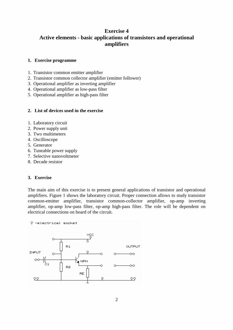
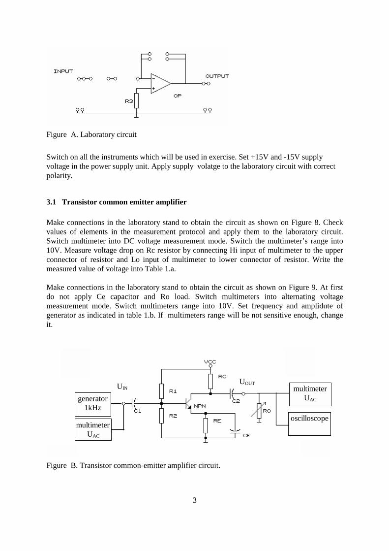
The main aim of this exercise is to present general applications of transistor and operationalamplifiers. Figure 1 shows the laboratory circuit. Proper connection allows to study transistorcommon-emitter amplifier, transistor common-collector amplifier, op-amp invertingamplifier, op-amp low-pass filter, op-amp high-pass filter. The role will be dependent onelectrical connections on board of the circuit.
3
Figure A. Laboratory circuit
Switch on all the instruments which will be used in exercise. Set +15V and -15V supplyvoltage in the power supply unit. Apply supply volatge to the laboratory circuit with correctpolarity.
3.1 Transistor common emitter amplifier
Make connections in the laboratory stand to obtain the circuit as shown on Figure 8. Checkvalues of elements in the measurement protocol and apply them to the laboratory circuit.Switch multimeter into DC voltage measurement mode. Switch the multimeter’s range into10V. Measure voltage drop on Rc resistor by connecting Hi input of multimeter to the upperconnector of resistor and Lo input of multimeter to lower connector of resistor. Write themeasured value of voltage into Table 1.a.
Make connections in the laboratory stand to obtain the circuit as shown on Figure 9. At firstdo not apply Ce capacitor and Ro load. Switch multimeters into alternating voltagemeasurement mode. Switch multimeters range into 10V. Set frequency and amplidute ofgenerator as indicated in table 1.b. If multimeters range will be not sensitive enough, changeit.
multimeterUAC
generator1kHz
multimeterUAC
oscilloscope
UINUOUT
Figure B. Transistor common-emitter amplifier circuit.
4
Apply to the circuit Ce capacitor and fill the Table 2. Then apply to the circuit Ro resistor(decade resistor) and fill in Table 3.
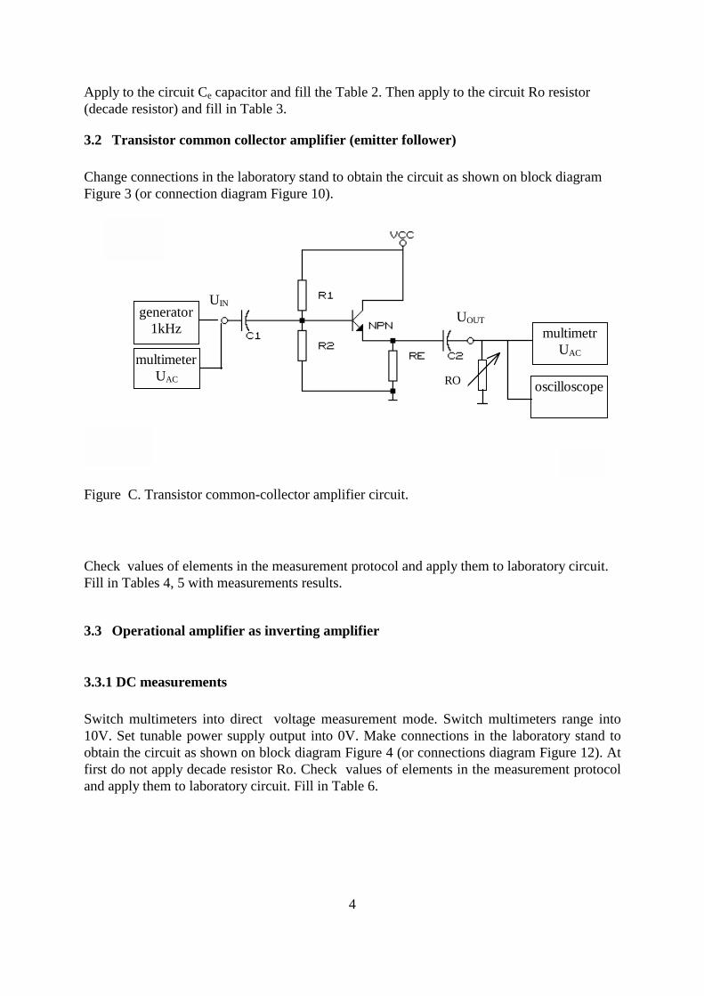
3.2 Transistor common collector amplifier (emitter follower)
Change connections in the laboratory stand to obtain the circuit as shown on block diagramFigure 3 (or connection diagram Figure 10).
multimeterUAC
generator1kHz multimetr
UAC
oscilloscopeRO
UIN
UOUT
Figure C. Transistor common-collector amplifier circuit.
Check values of elements in the measurement protocol and apply them to laboratory circuit.Fill in Tables 4, 5 with measurements results.
3.3 Operational amplifier as inverting amplifier
3.3.1 DC measurements
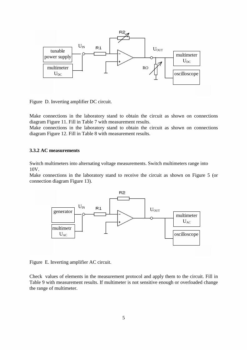
Switch multimeters into direct voltage measurement mode. Switch multimeters range into10V. Set tunable power supply output into 0V. Make connections in the laboratory stand toobtain the circuit as shown on block diagram Figure 4 (or connections diagram Figure 12). Atfirst do not apply decade resistor Ro. Check values of elements in the measurement protocoland apply them to laboratory circuit. Fill in Table 6.
5
multimeterUDC
tunablepower supply multimeter
UDC
oscilloscopeRO
UIN UOUT
Figure D. Inverting amplifier DC circuit.
Make connections in the laboratory stand to obtain the circuit as shown on connectionsdiagram Figure 11. Fill in Table 7 with measurement results.Make connections in the laboratory stand to obtain the circuit as shown on connectionsdiagram Figure 12. Fill in Table 8 with measurement results.
3.3.2 AC measurements
Switch multimeters into alternating voltage measurements. Switch multimeters range into10V.Make connections in the laboratory stand to receive the circuit as shown on Figure 5 (orconnection diagram Figure 13).
multimetrUAC
generatormultimeter
UAC
oscilloscope
UIN UOUT
Figure E. Inverting amplifier AC circuit.
Check values of elements in the measurement protocol and apply them to the circuit. Fill inTable 9 with measurement results. If multimeter is not sensitive enough or overloaded changethe range of multimeter.

6
3.4 Operational amplifier as low-pass filter
Change connections in the laboratory stand to obtain the circuit as shown on Figure 6 (orconnection diagram Figure 14).
multimeterUAC
generatormultimeter
UAC
oscilloscope
UIN UOUT
Figure F. Low-pass filter circuit.
Check values of elements in the measurement protocol and apply them to the circuit. Fill inTable 10 with measurement results. Change multimeter range if readout is overloaded or outof range.
3.5 Operational amplifier as high-pass filterChange connections in the laboratory stand to obtain the circuit as shown on Figure 7 (orconnection diagram Figure 15).
multimeterUAC
generatormultimeter
UAC
oscilloscope
UIN UOUT
Figure G. High-pass filter circuit.
Check values of elements in the measurement protocol and apply them to the circuit. Fill inTable 11 with measurement results. Change multimeter range if readout is overloaded or outof range.
4. Measurement data evaluation
For measurement data evaluation check protocol.
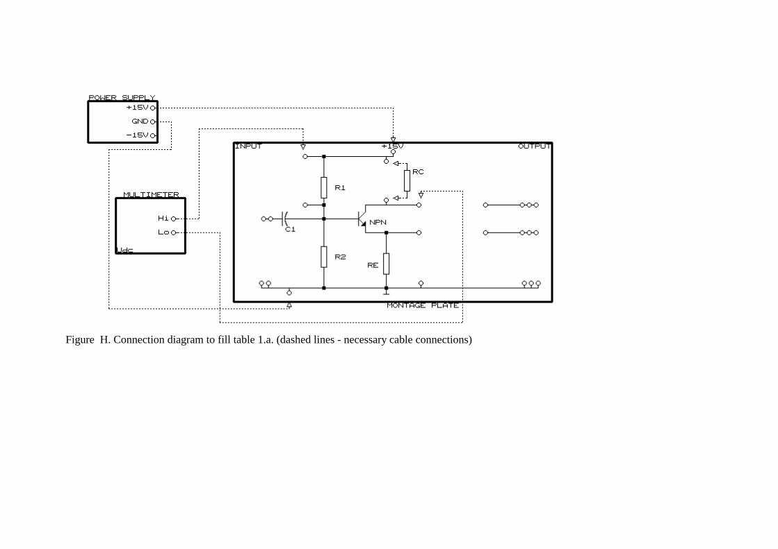
Figure H. Connection diagram to fill table 1.a. (dashed lines - necessary cable connections)

8
Figure 9. Connection diagram to fill tables 1.b., 2. and 3. (dashed lines - necessary cable connections)
9
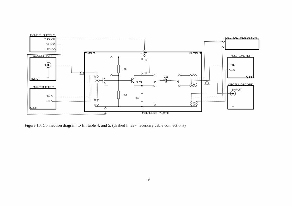
Figure 10. Connection diagram to fill table 4. and 5. (dashed lines - necessary cable connections)

10
Figure 11. Connection diagram to fill table 6. and 7. (dashed lines - necessary cable connections)
11
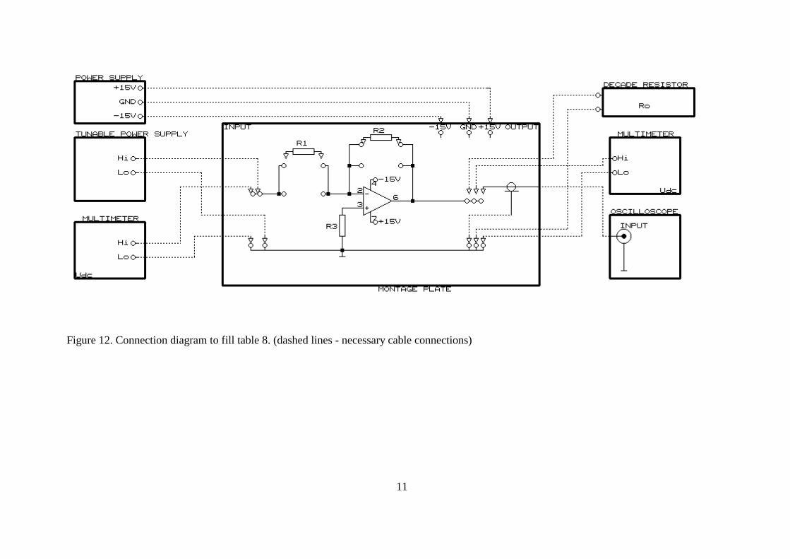
Figure 12. Connection diagram to fill table 8. (dashed lines - necessary cable connections)

12
Figure 13. Connection diagram to fill table 9. (dashed lines - necessary cable connections)
13
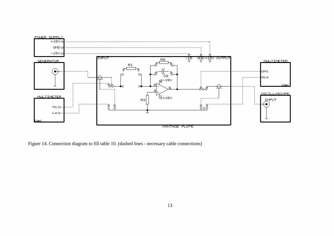
Figure 14. Connection diagram to fill table 10. (dashed lines - necessary cable connections)
14
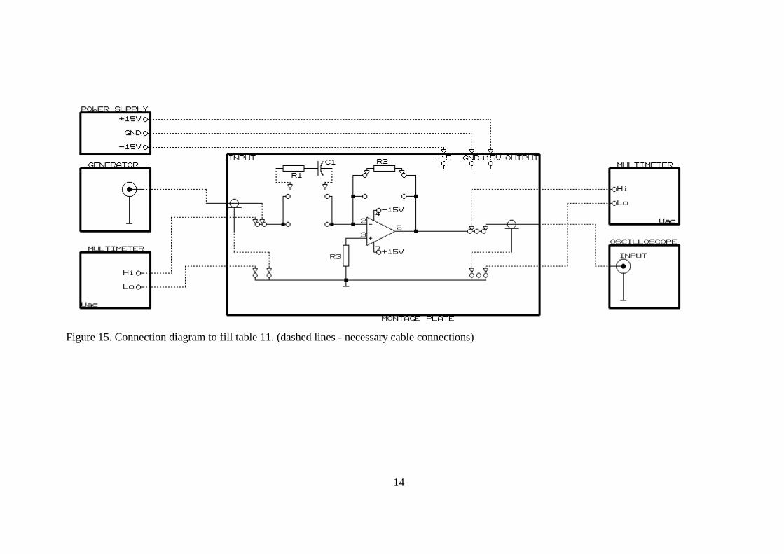
Figure 15. Connection diagram to fill table 11. (dashed lines - necessary cable connections)

5. Literature
P.Horowitz, W.Hill, Sztuka elektroniki, pp.72-121, 187-247.
6. Bipolar Junction Transistors and their applications as amplifier
The bipolar junction transistor is constructed with three doped semiconductor regionsseparated by two PN junctions. The three regions are called emitter, base and collector. Thereare two types of bipolar transistors: PNP (two P regions separated by N region) and NPN (twoN regions separated by P region). The PN junction joining the base region and the emitterregion is called the base-emitter junction. The junction joining the base region and thecollector region is called the base-collector junction. Wire leads connected to each of threeregions are named E, B and C for emitter, base and collector respectively.Figure shows the schematic symbols for the NPN and PNP bipolar transistors.
Figure 16. Transistor symbols
The term bipolar refers to the use of both holes and electrons as carriers in the transistorstructure.
6.1 Common - emitter amplifier
Figure 16 shows a typical common - emitter amplifier. C1 and C2 are coupling capacitorsused to pass the signal into and out of the amplifier so that the source or load will not affectthe DC bias voltage. CE capacitor is a bypass capacitor that shorts the AC emitter signalvoltage to ground without disturbing the DC emitter voltage. Because of the bypass capacitor,the emitter is at signal ground (but not DC ground), thus making the circuit a common -emitter amplifier. The purpose of the bypass capacitor is to increase the signal voltage gain.The voltage gain of the CE amplifier without the bypass capacitor shorting RE is:
A UU
I RI re R
Rre Rv
out
in
C C
E E
C
E
= =+
≅+( ) where re
mVIE
≅ 25
The voltage gain of the CE amplifier with the bypass capacitor shorting RE is:
A Rrev
C≅ where remVIE
≅ 25
16
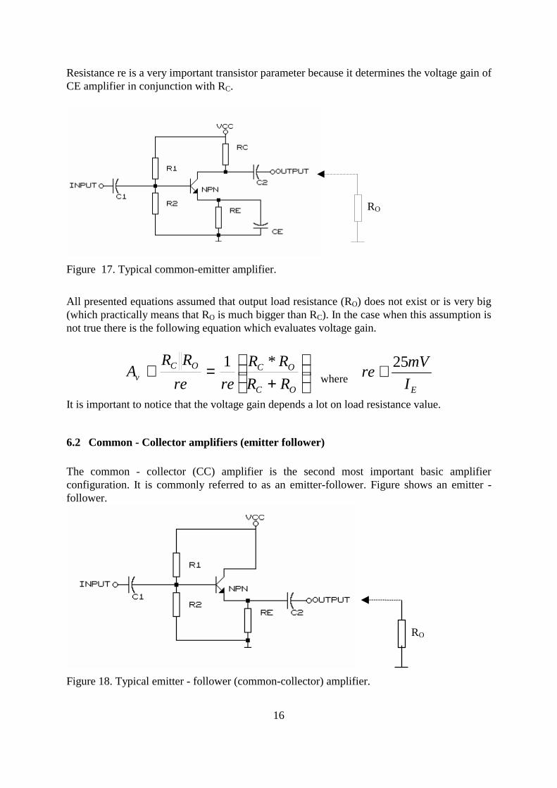
Resistance re is a very important transistor parameter because it determines the voltage gain ofCE amplifier in conjunction with RC.
Figure 17. Typical common-emitter amplifier.
All presented equations assumed that output load resistance (RO) does not exist or is very big(which practically means that RO is much bigger than RC). In the case when this assumption isnot true there is the following equation which evaluates voltage gain.
+
=≅OC
OCOCv RR
RRrere
RRA *1
where remVIE
≅ 25
It is important to notice that the voltage gain depends a lot on load resistance value.
6.2 Common - Collector amplifiers (emitter follower)
The common - collector (CC) amplifier is the second most important basic amplifierconfiguration. It is commonly referred to as an emitter-follower. Figure shows an emitter -follower.
Figure 18. Typical emitter - follower (common-collector) amplifier.
RO
RO

17
The voltage gain of the CC amplifier is:
AUU
I RI re R
Rre Rv
out
in
E E
E E
E
E
= =+
=+
≅( )
1
It is important to notice that the gain is always lower than 1. If re is much lower than RE(which is usually true), then a good approximation for the value of gain is 1.
Again all presented equations assumed that output load resistance (RO) does not exist or isvery big. In the case when this assumption is not true there is the following equation whichevaluates voltage gain.
AR R
R R revE O
E O
≅+( ) where re
mVIE
≅ 25
It is important to notice that the voltage gain even with very small load resistance does notpractically change the value. This is a very important feature of emitter follower and indicatesthat output resistance is very small. Input resistance of emiter follower is dependent on loadresistance. This feature is called transformation of resistance.
7. Operational Amplifiers (OP) and their applications
The operational amplifier is a linear integrated circuit which typically consists of two or moredifferential amplifier stages. As we will not go into details how OP is build it is enough to saythat OP has two input terminals (called the inverting input and the noninverting input) and oneoutput terminal. The typical OP operates with two DC supply voltages, one positive and theother negative. The standard OP symbol is shown in Figure 19.
Figure 19. Operational Amplifier symbol
The main characteristic of OP can be illustrated by equation:

18
VOUTPUT=A*(VINPUT+ - VINPUT-)where A is open-loop voltage gain (usually bigger than 10000). Also input impedance is verybig (close to infinite) and output impedance is very small (close to zero).
Application of OP as amplifier usually using a negative feedback design. This feedbackstabilizes the gain and increases frequency response. Negative feedback takes a portion of theoutput and applies it back out of the phase with the input, creating an effective reduction ingain. This gain is called closed-loop gain and is independent of open-loop gain.
7.1 OP as inverting amplifier
The circuit shown in the Figure represents OP connected as an inverting amplifier.
Figure 20. Inverting amplifier
To understand how this amplifier is working and to calculate close-loop gain, let’s assumethat an input impedance of OP has infinite value (what is good approximation). The infiniteinput impedance implies zero current to the inverting input. If there is zero current flowthrough the input impedance, then there must be no voltage drop between the inverting andnoniverting inputs. That means, the voltage at the inverting input is zero because the otherinput is grounded. The zero voltage at the inverting input terminal is referred to as virtualground. On this basis we can calculate closed-loop voltage gain.
19
I UR
I UR
I I
A UU
RR
Rout
RIN
R R
out
IN
22
11
1 2
2
1
= −
=
=
= = −
This clearly shows, that the closed-loop gain is independent of the OP internal open-loop gain.Thus, the negative feedback stabilizes the voltage gain. The negative sign indicates inversion.
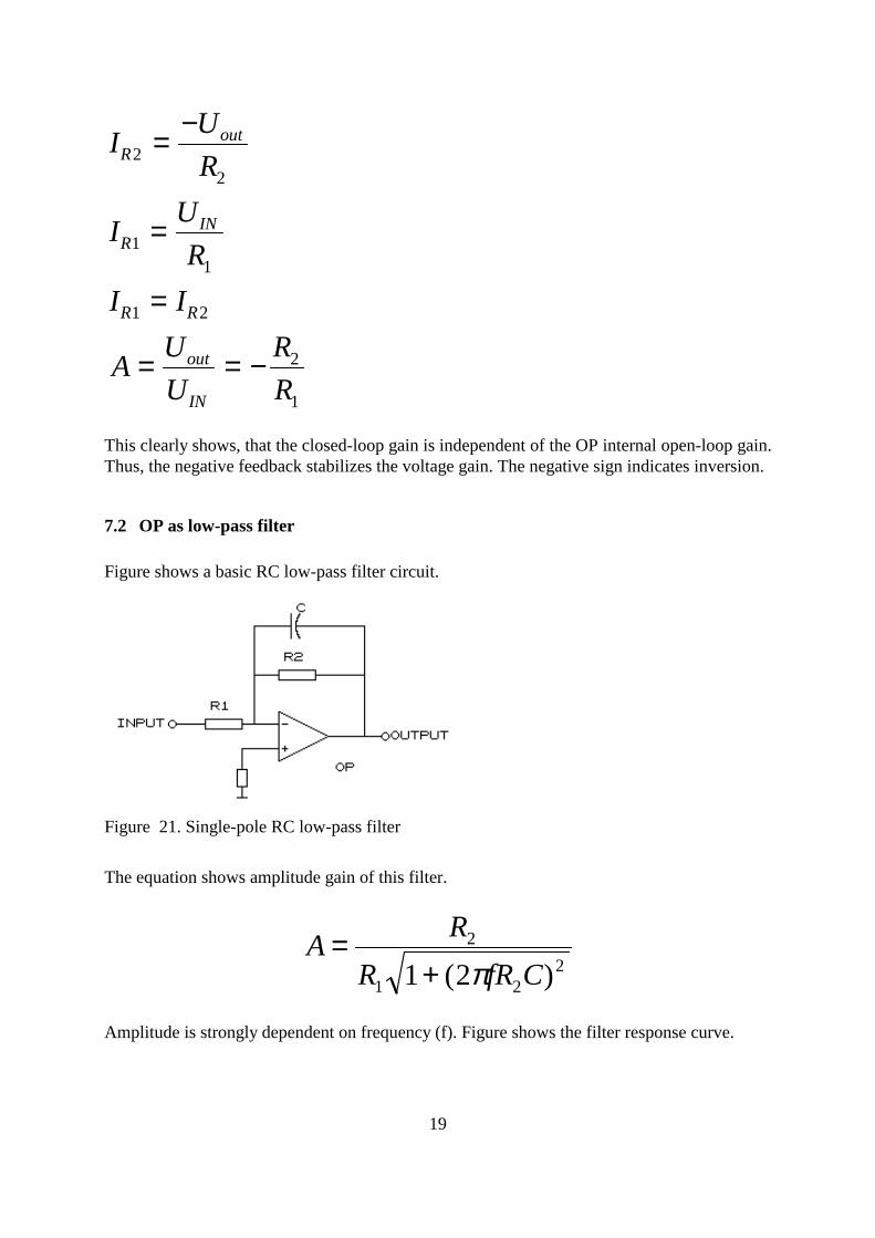
7.2 OP as low-pass filter
Figure shows a basic RC low-pass filter circuit.
Figure 21. Single-pole RC low-pass filter
The equation shows amplitude gain of this filter.
A RR fR C
=+
2
1 221 2( )π
Amplitude is strongly dependent on frequency (f). Figure shows the filter response curve.
20
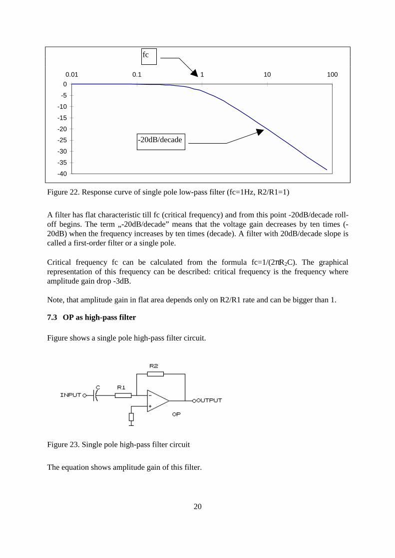
Figure 22. Response curve of single pole low-pass filter (fc=1Hz, R2/R1=1)
A filter has flat characteristic till fc (critical frequency) and from this point -20dB/decade roll-off begins. The term „-20dB/decade” means that the voltage gain decreases by ten times (-20dB) when the frequency increases by ten times (decade). A filter with 20dB/decade slope iscalled a first-order filter or a single pole.
Critical frequency fc can be calculated from the formula fc=1/(2πR2C). The graphicalrepresentation of this frequency can be described: critical frequency is the frequency whereamplitude gain drop -3dB.
Note, that amplitude gain in flat area depends only on R2/R1 rate and can be bigger than 1.
7.3 OP as high-pass filter
Figure shows a single pole high-pass filter circuit.
Figure 23. Single pole high-pass filter circuit
The equation shows amplitude gain of this filter.
-40
-35
-30
-25-20
-15
-10
-5
00.01 0.1 1 10 100
-20dB/decade
fc
21
A fR CfR C
=+2
1 22
12
ππ( )
Amplitude is strongly dependent on frequency (f). Figure shows the filter response curve.
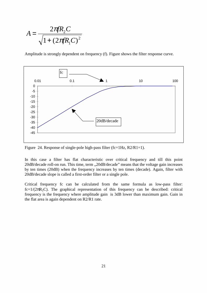
Figure 24. Response of single-pole high-pass filter (fc=1Hz, R2/R1=1).
In this case a filter has flat characteristic over critical frequency and till this point20dB/decade roll-on run. This time, term „20dB/decade” means that the voltage gain increasesby ten times (20dB) when the frequency increases by ten times (decade). Again, filter with20dB/decade slope is called a first-order filter or a single pole.
Critical frequency fc can be calculated from the same formula as low-pass filter:fc=1/(2πR2C). The graphical representation of this frequency can be described: criticalfrequency is the frequency where amplitude gain is 3dB lower than maximum gain. Gain inthe flat area is again dependent on R2/R1 rate.
-45-40-35-30-25-20-15-10-500.01 0.1 1 10 100
20dB/decade
fc