Embed Size (px)
Citation preview
Dynamic Behavior of the Triboelectric Chargesand Structural Optimization of the FrictionLayer for a Triboelectric NanogeneratorNuanyang Cui,†,‡ Long Gu,§ Yimin Lei,†,‡ Jinmei Liu,§ Yong Qin,§ Xiaohua Ma,*,†,‡ Yue Hao,*,†,‡
and Zhong Lin Wang∥
†School of Advanced Materials and Nanotechnology and ‡Wide Bandgap Semiconductor Technology Disciplines State KeyLaboratory, Xidian University, Xi’an 710071, China§Institute of Nanoscience and Nanotechnology, Lanzhou University, Lanzhou 730000, China∥School of Material Science and Engineering, Georgia Institute of Technology, Atlanta, Georgia 30332, United States
*S Supporting Information
ABSTRACT: Seeking to increase the triboelectric chargedensity on a friction layer is one of the most basic approachesto improve the output performance of triboelectric nano-generators (TENGs). Here, we studied the storage mechanismof triboelectric charge in the friction layer and discussed thefunction of carrier mobility and concentration in the charge-storing process. As guided by these results, a kind of compositestructure is constructed in the friction layer to adjust the depthdistribution of the triboelectric charges and improve the outputperformance of TENGs. To further elucidate this theory, asimple TENG, whose negative friction layer is a compositestructure by integrating polystyrene (PS) and carbon nanotubes (CNTs) into polyvinylidene fluoride (PVDF), wasfabricated, and its performance test was also carried out. Comparing with a pure PVDF friction layer, the compositefriction layer can raise the triboelectric charge density by a factor of 11.2. The extended residence time of electrons in thefriction layer is attributed to a large sum of electron trap levels from PS.
KEYWORDS: triboelectrification, nanogenerator, composite friction layer, triboelectric charge, charge storage
Recently, the triboelectric nanogenerator (TENG) basedon coupling of a triboelectric effect and electrostaticinduction has been extensively developed for harvesting
mechanical energy from ambient environment.1 Unlike atraditional chemical battery with limited lifespan2 and theneed for frequent replacement or recharging, a TENG candirectly translate mechanical energy into electrical energy andpower the functional electronics instantly. Although many otherapproaches based on different mechanisms have beendemonstrated for effectively harvesting mechanical energy,such as piezoelectric nanogenerators,3−12 electromagneticgenerators,13,14 and electrostatic generators,15 TENGs aremore dominant in power output and energy conversionefficiency.16−18 This makes TENGs most likely to be theenergy supply for portable electronics19−21 and even possibly tobe used for large-scale power generation in the near future.The working process of TENGs can be basically divided into
two steps: separation process of positive and negative chargescaused by friction or contact and an electricity output processinduced by electrostatic induction. The latter step is mainlyrelated to the device structure design, which usually focuses on
solving the problem of the device’s adaptability in differentenvironments.22−24 The first step, however, is mostly importantfor the output of TENG because both the current and voltageoutput are proportional to the triboelectric charge density onthe friction layer. Research in recent years suggested thatmatching appropriate materials and building surface micro-structure can greatly increase the triboelectric charge densityand the output of a TENG.25−27 However, these results areeither experimental outcomes or simple, qualitative theoreticalanalyses. Limited research is available about the fundamentalmechanism of the triboelectrification process. Therefore, wehave no definite guidelines on how to effectively adjust thetriboelectric charge density in the friction layer.Actually, the triboelectrification process can be further
divided into three subprocesses: the generation of thetriboelectric charges, the storage of the charges, and the loss
Received: March 25, 2016Accepted: April 29, 2016
Artic
lewww.acsnano.org
© XXXX American Chemical Society A DOI: 10.1021/acsnano.6b02076ACS Nano XXXX, XXX, XXX−XXX

of the charge, respectively. First, it is only possible to know thetendency of materials to gain or lose electrons based on thetriboelectric series, but the issues of most concern are the exactyield of triboelectric charges (TCY) in a certain condition aswell as its influence factor and extent. Second, after the positiveand negative charges are separated, the storage position oftriboelectric charges still needs to be considered. Third, ourprevious experiments indicated that the triboelectric chargestored in the friction layer will decay along with time. However,the factors that affect the process and the influence degree arestill mysteries until now. If all of these problems can be figuredout, the performance of TENGs can be further improved.In this work, the relationship between the friction layer
thickness and the transport process of triboelectric charges in apolyvinylidene fluoride (PVDF) film are investigated in detail.It is noticed that if the thickness of the friction layer is largerthan the storage depth, the stored charge can reach a maximum,and the excess increase of the storage depth does not contributeto the charge accumulation. More importantly, based on thecalculated results, a dielectric layer and a transport layer wereadded between the PVDF layer and the electrode. Thismultilayer structure design provided a factor of 11.2 improve-ment for the output performance of the TENG. As a generalconclusion, the study of the transport process of triboelectriccharges in the friction layer provides a new efficient approach toguide our work in TENG research.
RESULTS AND DISCUSSIONMonolayer Friction Layer. First, a model for the
generation, transport, and loss process of the triboelectriccharge was established. As seen in Figure 1a, the orange partrepresents the negative friction layer, which will captureelectrons from the positive friction layer (top aluminumelectrode in Figure 1a) during the triboelectrification process.As the electrons are accumulated on the contact surface, thepositive charges can be induced into the electrode. As shown inthe schematic, an electric field will be set up between thecontact surface and electrode, and the electric field direction isvertically upward. Therefore, two electron transfer modes exist:a drift process caused by the electric field and a diffusionprocess caused by the concentration gradient of electrons. Theloss of the triboelectric electrons comes from two aspects: oneis adsorbing positively charged ions or particles from air and theother one is the combination with the induced positive chargeson the electrode. In order to simplify the calculation, severalassumptions should be put forward:
(1) When the driving force is constant, the TCY is alsoconstant for a moment.
(2) Considering the actual electric field intensity is largeenough in our experiment, the diffusion process can beneglected.
(3) We take into account only the charge loss caused by thecombination of electrons and the induced positivecharges on the electrode.
(4) We neglect the impact of the trap levels on thetriboelectric electrons temporarily.
Figure 1. (a) Schematic of the transport process of triboelectric electrons in the negative friction layer of a TENG. (b) Theoreticaltriboelectric charge distribution in the friction layer. The red line is the result of only taking the carrier mobility μ0 into account, and the blackline is the result considering both carrier mobility μ0 and its intrinsic carrier density n0. (c) Theoretical relationship between the total storagecharge and the thickness of the friction layer. (d) Measured total surface charge in the PVDF friction layer with different thicknesses. Thecorresponding short-circuit currents are shown in the inset.
ACS Nano Article
DOI: 10.1021/acsnano.6b02076ACS Nano XXXX, XXX, XXX−XXX
B
(5) Compared with the sample thickness, the area of thecontact surface is large enough that the sample can beassumed as one-dimensional.
Under the above assumptions the electron drift process ismodeled by the drift equation and solved by the recursionmethod. The details are shown in the Supporting Information.As PVDF is one of the most commonly used negative
materials for TENGs, it will be the major research subject inthis work. The carrier mobility and intrinsic carrier density ofPVDF are μ0 = 1.2 × 10⁻¹⁰ cm2/V·s and n0 = 5.5 × 1016 cm−3,respectively. The contact surface area is about 1 cm2. The TCYis approximately equal to 0.1 nC/s (this is an average valuemeasured within 10 s after the TENG begins to work, takenfrom our following experimental test, shown in Figure 6).Figure 1b shows the theoretical triboelectric charge distributionthrough the depth of the friction layer under enough frictiontime. The red line is the result with only the PVDF carriermobility being taken into account, and the black line is the
result when considering both PVDF carrier mobility and itsintrinsic carrier density. Accounting for the carrier mobilitysolely, the triboelectric charge density will decrease with anincrease in the depth of the PVDF layer but never reach zero.Considering the relationship between total quantity of thetriboelectric charge and the thickness of the PVDF layer(Figure 1c), it is noticed that the thicker the friction layer, themore triboelectric charge that will be obtained. Actually, theintrinsic carriers in PVDF can promote the combination of thetriboelectric electrons, leading to the conversion of triboelectriccharge density to zero quickly in the friction layer (black line inFigure 1b). When the PVDF thickness reaches about 4 μm,there is a maximum value for the total charge amount stored inthe PVDF layer, and the excess thickness does not contribute tothe charge accumulation.To verify the calculated results through experiments, nine
TENGs were fabricated, in which the negative friction layers arePVDF films with different thicknesses prepared by spin-coatingand the positive friction layers are all aluminum foil. With
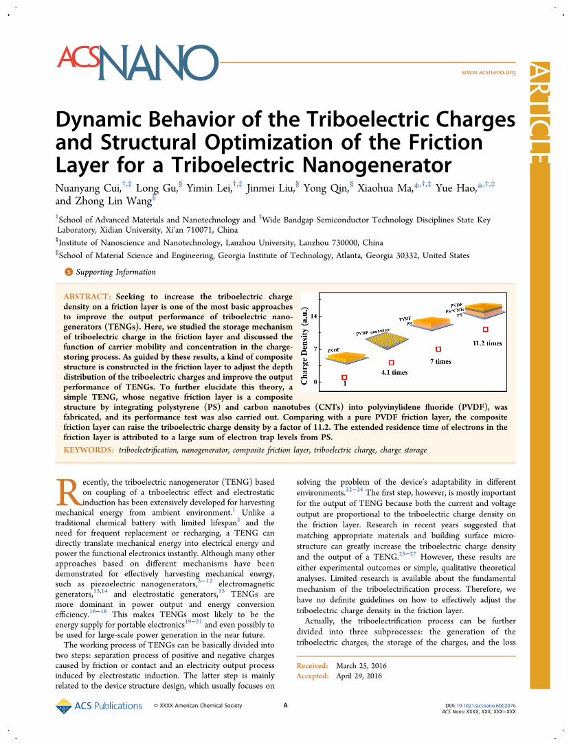
Figure 2. (a and b) Theoretical relationship between the total storage charge and the thickness of the friction layer with different carriermobility and intrinsic carrier density. (c and d) Theoretical triboelectric charge distribution in the bistratal friction layer. (e and f) Theoreticalrelationship between the total storage charge and the thickness of the bistratal friction layer.
ACS Nano Article
DOI: 10.1021/acsnano.6b02076ACS Nano XXXX, XXX, XXX−XXX
C
preparatory work completed, these TENGs were set to workfor 30 min under the same driving condition. The short-circuit
current of these devices was collected and are shown in theinset of Figure 1d. Figure 1d shows the change rule of the areal
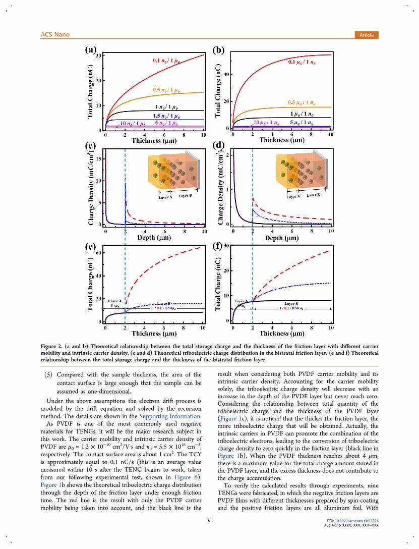
Figure 3. Short currents of device A (a), device B (b), and device C (c). Device A has a 12 μm thick PS friction layer and 3.5 μm thick PVDFdielectric layer; device B has a 3.5 μm thick PVDF friction layer only, and device C has a 3.5 μm thick PVDF friction layer and 12 μm thick PSdielectric layer. (d) Peak currents and total surface charge of these three devices.
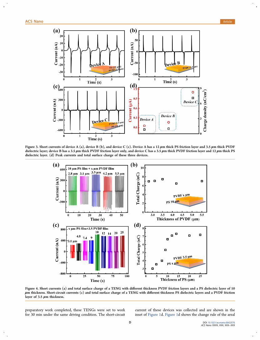
Figure 4. Short currents (a) and total surface charge of a TENG with different thickness PVDF friction layers and a PS dielectric layer of 10μm thickness. Short-circuit currents (c) and total surface charge of a TENG with different thickness PS dielectric layers and a PVDF frictionlayer of 3.5 μm thickness.
ACS Nano Article
DOI: 10.1021/acsnano.6b02076ACS Nano XXXX, XXX, XXX−XXX
D

density of the total triboelectric charge with the increase of thePVDF layer thickness. Similar to the theoretical calculation, thetriboelectric charge areal density in the PVDF layer increaseswith increasing its thickness at the beginning and then reaches astable status. In the calculation process above, the theoreticalmodel has been simplified, leading to the deviation of theresults from the experimental outcomes. However, from theirsimilar variation trend, a further understanding of thetriboelectric charge transport and storage processes can beobtained. Further analysis about the effect of the carriermobility and intrinsic carrier density on the storage oftriboelectric charge has been carried out, as shown in Figure2. It is noticed that the triboelectric charge distribution changeswith adjusting these two parameters independently, as shown inFigure S2. When the carrier mobility is reduced to 10%, thetotal amount of the triboelectric charge stored in the PVDFlayer is increased about 7 times (Figure 2a). Then on reducingthe intrinsic carrier density, the storage depth is obviously
increased while the incremental amount of the triboelectriccharge is less than that in reducing the carrier mobility. Thismeans that a smaller intrinsic carrier density can significantlyincrease the valid thickness of the friction layer (Figure 2b).Therefore, an ideal material for TENG needs to have a largerTCY, smaller carrier mobility, as well and smaller intrinsiccarrier density, but these requirements can hardly be metsimultaneously.
Double-Layer Composite Friction Layer. To assemblethe advantages of different materials into one, a compositestructure model is attempted to be established for the frictionlayer. First, layer A is selected as the contact surface, whosemobility and intrinsic carrier density are μ0 and n0, respectively.Then a thick dielectric layer, layer B, is added between layer Aand the electrode. This dielectric layer should have a smallercarrier mobility or smaller intrinsic carrier density. Thesimulation calculation results are shown in Figure 2c−f. It isproved theoretically that a composite layered structure can
Figure 5. (a) Theoretical triboelectric charge distribution in the friction layer for three different states: ideal states (no TCY decay) (blackline), considering the TCY decay (blue dotted line), and adding a transport layer on the surface (red dot-dashed line). (b) Theoreticalrelationship between the total storage charge and the thickness of the friction layer for the three different states. (c−f) Measured total surfacecharge in the friction layer of TENGs with different structures.
ACS Nano Article
DOI: 10.1021/acsnano.6b02076ACS Nano XXXX, XXX, XXX−XXX
E

improve the total storage charge and storage depthdramatically. To verify the feasibility of this method, TENGdevices were prepared accordingly: device A has a PS frictionlayer with a thickness of 12 μm and a PVDF dielectric layerwith a thickness of 3.5 μm. Device B has only a PVDF frictionlayer with a thickness of 3.5 μm, while device C has a PVDFfriction layer with a thickness of 3.5 μm and a 12 μm PSdielectric layer. The positive friction layers of these TENGdevices are all aluminum foils. After making these TENGs workfor 30 min under the same driving conditions, the short-circuitcurrent of these devices are collected respectively, as shown inFigure 3a−c. Figure 3d illustrates the current peak values andthe surface charge density of the three devices. Compared withPVDF, PS is not an ideal negative friction material for TENGdue to its weaker ability to capture electrons from the positivefriction layer; thus both the current peak and surface chargedensity of device A are smaller than those of device B. Theintrinsic carrier density of PS is smaller than that of PVDF, andthe electron mobility of PS is also smaller than that of PVDFbecause PS has abundant trap levels of electrons. These makePS one of the most suitable dielectric materials. TENG deviceC, with the PS dielectric layer, shows an amazing charge storageability that is 7 times as much as that in device B, with the purePVDF layer. To investigate the effect of the PVDF−PScomposite structure in depth, we prepared two groups of newTENG devices. One group has a varied thickness of the PVDFfriction layer while keeping the PS layer the same. The othergroup has a varied thickness of the PS dielectric layer whilekeeping the PVDF layer the same. With preparatory workcompleted, the outputs of these devices were obtained,respectively. Figure 4a is the short-circuit currents of devicesin group 1, and Figure 4b shows the surface total chargeaccumulated in the composite layer. Unlike the situation in
Figure 1d, the thickness variation of the PVDF layer does nothave a significant influence on the stored charges. From theabove results it can be surmised that most of the triboelectriccharges are stored in the PS dielectric layer, and this is soonconfirmed by the test results of devices in group 2 (Figure 4 cand d). As the thickness of the PS layer was increased from 3.1μm to 14 μm, the accumulated charge increases from 3 nC/cm2
to 7.3 nC/cm2 and then reaches a stable status. This trend iscompletely consistent with the pure PVDF device (Figure 1d)and the theoretical results (Figure 2c and d).
Three-Layer Composite Friction Layer. Although theexperimental result is well consistent with the calculated resultin the variation trend of triboelectric charges, there exists agreat gap between the total charge quantity of these two results.With a pure PVDF device, for example, the calculated value ofthe maximal stored charge is 8 nC/cm2, but the experimentalresult is only 1.5 nC/cm2. In our opinion, this gap probablycomes from the simplification of the theoretical model. Thetwo most important points can be summarized as thecombination of triboelectric charge and ions or chargedparticles in the air as well as the impact of the TCY. Atpresent, only the second point is addressed in this study. In theprevious calculation, the TCY is simply regarded as a constant.However, the triboelectric charge that enters the friction layerearly would in turn block the entrance of other charges, asshown in the left inset in Figure 5a. In this way, the TCY willdecrease gradually with the accumulation of triboelectriccharges. If there really exists an attenuation effect on theTCY, the most important factors must be the quantity oftriboelectric charge and the distance between the contactsurface and the charge. The more the charges are accumulated,the smaller the TCY. Also, the shallower the storage depth ofcharges, the smaller the TCY. In order to solve the problemtheoretically, two assumptions should be put forward:
(1) Only the charge stored at a depth of 0 to 2 μm affects theTCY, and all of these charges have the same impactdegree on the TCY.
(2) Along with the increase of the accumulated charge, theTCY tends to decay exponentially. The attenuationfunction can be described as
= × −I a q Aexp( / )c (1)
Here Ic is the actual TCY, a is the ideal maximum TCY, q is thetotal charge quantity accumulated at a depth from 0 to 2 μm,and A is an attenuation coefficient. When considering theattenuation of TCY, the new calculated results (blue line inFigure 5a and b) are significantly smaller than the early results(black line in Figure 5a and b). The most important thing tothe TENG is its output performance. However, now thecharges close to the contact surface will restrain the entering ofnew charges; thus a method to lead the superficial charges to adeep position should be found. On the basis of the aboveanalysis, we can replace a thin layer on the very surface with anew transport layer that has a high conductivity. In this way, theaccumulated charge in the top surface layer will become less,and accordingly the attenuation effect on TCY will also beweakened; the schematic is shown in the right inset in Figure5a. The red lines in Figure 5a and b are the calculated resultswhen the carrier mobility and intrinsic carrier density of thesurface layer of a thickness of 2 μm decreased by 5 timescompared with the original value. The red line in Figure 5bobviously shows that this adjustment is very effective.
Figure 6. (a) Improvement effects of different composite frictionlayer structure. (b) Accumulation process and decay process of thetriboelectric charge for a pure PVDF TENG device (red circle) anda PVDF-PS TENG device (black square).
ACS Nano Article
DOI: 10.1021/acsnano.6b02076ACS Nano XXXX, XXX, XXX−XXX
F

To form the transport layer mentioned above in thefollowing experiments, 0.7 wt % carbon nanotubes (CNTs)were added into PVDF or PS. This transport layer should besandwiched between the friction layer and the dielectric layerrather than put on the outermost layer; if not, triboelectriccharges will be lost through the transport layer. As shown inFigure 5c, when the transport layer is put on the outermostlayer, the total accumulated charge (red point) is less than thatin the pure PVDF device (black point). If this transport layer isadded between two PVDF layers, the charge density in thecomposite layer is improved significantly and is even larger thanthe maximum charge density of the pure PVDF device, asshown in Figure 5d. For the PVDF−PS composite layer device,the transport layer, which is composed of 99.3 wt % PS and 0.7wt % CNTs, was sandwiched between the PVDF layer and thePS layer; the charge storage capacity of these devices is shownin Figure 5e. The transport layer not only gives a better chargestorage capacity but also increases the storage depth of thetriboelectric charge. As we continue to increase the content ofCNTs in the PS transport layer, the total charge quantityincreases very slowly (Figure 5f), which means that the amountof stored charge increases more and more slowly whenincreasing the transport layer’s conductivity. This result isalso consistent with the calculation above. It is noticed that thestored charge decreases slower and slower along with theincrease in carrier mobility or density, as shown in Figure 2 aand b. In summary, the triboelectric charge density can go up 7times by adding a PS dielectric layer and 11.2 times by buildinga three-layer structure that includes a PVDF layer, a compositetransport layer, and a PS dielectric layer. However, in theprevious report, the PVDF nanowire structure can only increasethe charge density up to 4.1 times27 (Figure 6a).In addition, the charge accumulation process and its decay
process over time for the two kinds of TENGspure PVDFdevice (red circles in Figure 6b) and PVDF−PS compositelayer device (black squares in Figure 6b)were testedaccordingly. Here, a decay time τ is used to characterize theelectron storage capacity for different materials, which meansthe time it takes for 1/e charge to remain. For a pure PVDFdevice, the decay time τPVDF is only 22 min. However, when aPS dielectric layer is introduced, the decay time τPVDF−PSreaches up to 44 h. This is because most of the triboelectriccharges are stored in the PS layer; meanwhile, the abundanttrap levels of electrons in PS can bind the flowing electronseffectively.
CONCLUSIONIn summary, the transport and storage process of thetriboelectric charge in the friction layer was investigatedcomprehensively. On the basis of the theoretical analysis, weproposed two effective approaches to improve the outputperformance of the TENG. The first one is to add a PSdielectric layer between the PVDF friction layer and theelectrode. The areal density of the total triboelectric charge inthe new device is 6 times higher than that in the pure PVDFdevice. The other approach is to add a transport layer betweenthe friction layer and the dielectric layer or increase theconductivity of the middle layer by introducing a small amountof carbon nanotubes. This method can increase the triboelectriccharge yield effectively, and as such, the total charge quantity inthe friction layer could be further increased by a factor of 1.6.Aiming at improving the output performance, these twoapproaches can be widely used to guide the fabrication of
TENGs, which provides a solid foundation for TENG researchand development.
METHODSPreparation of the PVDF and PS Solutions. A 2.0 g amount of
PVDF was mixed with 8.0 g of N,N-dimethylformamide (DMF) in a50 mL triangular flask. The solution was stirred at 60 °C for 3 h andcooled to room temperature. A 3.0 g amount of PS was mixed with 8.0g of DMF in a 50 mL triangular flask; then it was stirred for 3 h toensure the dissolution of PS. All reagents were analytically pure andused without any further purification.
Fabrication of TENG Devices. First, to fabricate the negativefriction layer part of the TENG, a piece of glass slide with side lengthof 2.5 cm was prepared as substrate. Then the corresponding sizealuminum foil was adhered on the surface of this substrate by double-sided tape. After that, the negative friction layers were prepared on thesurface of the aluminum foil by the spin-coating method. By adjustingthe spin speed of coating, from 500 rpm to 4000 rpm, the thickness ofthe friction layer can be controlled easily. For the purpose offacilitating the comparison, all the different negative friciton layersshare a single positive friction layer part, which is composed of a glasssubstrate with a side lengh of 1 cm and a piece of aluminum foil affixedto it.
ASSOCIATED CONTENT*S Supporting InformationThe Supporting Information is available free of charge on theACS Publications website at DOI: 10.1021/acsnano.6b02076.
Calculated electron drift process in the friciton layer;figures comparing the triboelectric charge distributions inthe friction layers with different parameters (PDF)
AUTHOR INFORMATIONCorresponding Authors*E-mail: [email protected].*E-mail: [email protected] authors declare no competing financial interest.
ACKNOWLEDGMENTSResearch was supported by NSFC (Grant No. 61334002) andthe Fundamental Research Funds for the Central Universities(Grant Nos. JB161401 and JB161402).
REFERENCES(1) Fan, F.-R.; Tian, Z.-Q.; Wang, Z. L. Flexible TriboelectricGenerator. Nano Energy 2012, 1, 328−334.(2) Zou, Y.; Hu, X.; Ma, H.; Li, S. E. Combined State of Charge andState of Health Estimation Over Lithium Ion Battery Cell CycleLifespan for Electric Vehicles. J. Power Sources 2015, 273, 793−803.(3) Cui, N.; Wu, W.; Zhao, Y.; Bai, S.; Meng, L.; Qin, Y.; Wang, Z. L.Magnetic Force Driven Nanogenerators as a Noncontact EnergyHarvester and Sensor. Nano Lett. 2012, 12, 3701−3705.(4) Park, K. I.; Son, J. H.; Hwang, G. T.; Jeong, C. K.; Ryu, J.; Koo,M.; Choi, I.; Lee, S. H.; Byun, M.; Wang, Z. L. Highly Efficient,Flexible Piezoelectric PZT Thin Film Nanogenerator on PlasticSubstrates. Adv. Mater. 2014, 26, 2514−2520.(5) Mao, Y.; Zhao, P.; McConohy, G.; Yang, H.; Tong, Y.; Wang, X.Sponge Like Piezoelectric Polymer Films for Scalable and IntegratableNanogenerators and Self-Powered Electronic Systems. Adv. EnergyMater. 2014, 410.1002/aenm.201301624(6) Jeong, C. K.; Park, K.-I.; Son, J. H.; Hwang, G.-T.; Lee, S. H.;Park, D. Y.; Lee, H. E.; Lee, H. K.; Byun, M.; Lee, K. J. Self-PoweredFully Flexible Light Emitting System Enabled by Flexible EnergyHarvester. Energy Environ. Sci. 2014, 7, 4035−4043.
ACS Nano Article
DOI: 10.1021/acsnano.6b02076ACS Nano XXXX, XXX, XXX−XXX
G

(7) Jeong, C. K.; Park, K. I.; Ryu, J.; Hwang, G. T.; Lee, K. J. LargeArea and Flexible Lead Free Nanocomposite Generator Using AlkalineNiobate Particles and Metal Nanorod Filler. Adv. Funct. Mater. 2014,24, 2620−2629.(8) Hwang, G. T.; Park, H.; Lee, J. H.; Oh, S.; Park, K. I.; Byun, M.;Park, H.; Ahn, G.; Jeong, C. K.; No, K. Self-Powered CardiacPacemaker Enabled by Flexible Single Crystalline PMN PT Piezo-electric Energy Harvester. Adv. Mater. 2014, 26, 4880−4887.(9) Persano, L.; Dagdeviren, C.; Su, Y.; Zhang, Y.; Girardo, S.;Pisignano, D.; Huang, Y.; Rogers, J. A. High Performance PiezoelectricDevices Based on Aligned Arrays of Nanofibers of Poly (vinyl-idenefluoride-co-trifluoroethylene). Nat. Commun. 2013, 4, 1633.(10) Jeong, C. K.; Kim, I.; Park, K.-I.; Oh, M. H.; Paik, H.; Hwang,G.-T.; No, K.; Nam, Y. S.; Lee, K. J. Virus Directed Design of aFlexible BaTiO3 Nanogenerator. ACS Nano 2013, 7, 11016−11025.(11) Ramadoss, A.; Saravanakumar, B.; Lee, S. W.; Kim, Y.-S.; Kim, S.J.; Wang, Z. L. Piezoelectric Driven Self Charging SupercapacitorPower Cell. ACS Nano 2015, 9, 4337−4345.(12) Zi, Y.; Lin, L.; Wang, J.; Wang, S.; Chen, J.; Fan, X.; Yang, P. K.;Yi, F.; Wang, Z. L. Triboelectric Pyroelectric Piezoelectric Hybrid Cellfor High Efficiency Energy Harvesting and Self Powered Sensing. Adv.Mater. 2015, 27, 2340−2347.(13) Galchev, T.; McCullagh, J.; Peterson, R.; Najafi, K. HarvestingTraffic-Induced Vibrations for Structural Health Monitoring ofBridges. J. Micromech. Microeng. 2011, 21, 104005.(14) Beeby, S. P.; Torah, R.; Tudor, M.; Glynne-Jones, P.;O’Donnell, T.; Saha, C.; Roy, S. A Micro Electromagnetic Generatorfor Vibration Energy Harvesting. J. Micromech. Microeng. 2007, 17,1257.(15) Mitcheson, P. D.; Green, T. C.; Yeatman, E. M.; Holmes, A. S.Architectures for Vibration Driven Micropower Generators. J.Microelectromech. Syst. 2004, 13, 429−440.(16) Tang, W.; Jiang, T.; Fan, F. R.; Yu, A. F.; Zhang, C.; Cao, X.;Wang, Z. L. Liquid Metal Electrode for High PerformanceTriboelectric Nanogenerator at an Instantaneous Energy ConversionEfficiency of 70.6%. Adv. Funct. Mater. 2015, 25, 3718.(17) Lin, L.; Xie, Y.; Niu, S.; Wang, S.; Yang, P.-K.; Wang, Z. L.Robust Triboelectric Nanogenerator Based on Rolling Electrificationand Electrostatic Induction at an Instantaneous Energy ConversionEfficiency of∼ 55%. ACS Nano 2015, 9, 922−930.(18) Zi, Y.; Lin, L.; Wang, J.; Wang, S.; Chen, J.; Fan, X.; Yang, P. K.;Yi, F.; Wang, Z. L. Triboelectric Pyroelectric Piezoelectric Hybrid Cellfor High Efficiency Energy Harvesting and Self Powered Sensing. Adv.Mater. 2015, 27, 2340−2347.(19) Su, L.; Zhao, Z. X.; Li, H. Y.; Yuan, J.; Wang, Z. L.; Cao, G. Z.;Zhu, G. High Performance Organolead Halide Perovskite-Based Self-Powered Triboelectric Photodetector. ACS Nano 2015, 9, 11310−11316.(20) Li, X.; Yeh, M.-H.; Lin, Z.-H.; Guo, H.; Yang, P.-K.; Wang, J.;Wang, S.; Yu, R.; Zhang, T.; Wang, Z. L. Self-Powered TriboelectricNanosensor for Microfluidics and Cavity Confined SolutionChemistry. ACS Nano 2015, 9, 11056−11063.(21) Wang, S.; Mu, X.; Wang, X.; Gu, A. Y.; Wang, Z. L.; Yang, Y.Elasto-Aerodynamics-Driven Triboelectric Nanogenerator for Scav-enging Air Flow Energy. ACS Nano 2015, 9, 9554−9563.(22) Cui, N.; Gu, L.; Liu, J.; Bai, S.; Qiu, J.; Fu, J.; Kou, X.; Liu, H.;Qin, Y.; Wang, Z. L. High Performance Sound Driven TriboelectricNanogenerator for Harvesting Noise Energy. Nano Energy 2015, 15,321−328.(23) Cui, N.; Liu, J.; Gu, L.; Bai, S.; Chen, X.; Qin, Y. WearableTriboelectric Generator for Powering the Portable Electronic Devices.ACS Appl. Mater. Interfaces 2014, 7, 18225−18230.(24) Gu, L.; Cui, N.; Liu, J.; Zheng, Y.; Bai, S.; Qin, Y. PackagedTriboelectric Nanogenerator with High Endurability for SevereEnvironments. Nanoscale 2015, 7, 18049−18053.(25) Jeong, C. K.; Baek, K. M.; Niu, S.; Nam, T. W.; Hur, Y. H.; Park,D. Y.; Hwang, G.-T.; Byun, M.; Wang, Z. L.; Jung, Y. S.Topographically Designed Triboelectric Nanogenerator via BlockCopolymer Self-Assembly. Nano Lett. 2014, 14, 7031−7038.
(26) Tang, W.; Zhang, C.; Han, C. B.; Wang, Z. L. Enhancing OutputPower of Cylindrical Triboelectric Nanogenerators by SegmentationDesign and Multilayer Integration. Adv. Funct. Mater. 2014, 24, 6684−6690.(27) Zheng, Y.; Cheng, L.; Yuan, M.; Wang, Z.; Zhang, L.; Qin, Y.;Jing, T. An Electrospun Nanowire Based Triboelectric Nanogeneratorand Its Application in a Fully Self-Powered UV Detector. Nanoscale2014, 6, 7842−7846.
ACS Nano Article
DOI: 10.1021/acsnano.6b02076ACS Nano XXXX, XXX, XXX−XXX
H