Embed Size (px)
Citation preview
99 International Journal of Control Theory and Applications
Analysis and Evaluation of Sinusoidal Power clocked Adiabatic Logic Circuits
Analysis and Evaluation of Sinusoidal Power clocked Adiabatic LogicCircuits
Sandeep S*, Saraniya U*, P Sasipriya** and V S Kanchana Bhaaskaran*
* School of Electronics Engineering, VIT University, Chennai- 600 127, Tamil Nadu, IndiaE-mail: [email protected], [email protected], [email protected]** School of Electrical Engineering, VIT University, Chennai-600127, Tamil Nadu, IndiaE-mail: [email protected]
Abstract: Adiabatic switching that works based on the principle of charge recovery is one of the most promising nonconventional approaches for low power design of VLSI circuits. This paper focuses on the classification and comparisonof adiabatic circuits that are operated by sinusoidal clock signal. The performance analysis and comparison arecarried out by implementing the 8-bit array multiplier using static adiabatic logic families, namely, the QSERL,CEPAL and GFCAL. Comparison against the dynamic adiabatic logic families, namely, the CAL, PAL and SCALhave also been made. The performance of all of the circuits is evaluated in terms of the power dissipation for varyingrange of adiabatic frequencies. The drivability characteristics are also evaluated by using varying capacitive loads.Through post layout simulation of the full adder cells implemented using CEPAL and SCAL, the layout area requirementwhile keeping the layout density constant, for the static and dynamic adiabatic logic types is studied and compared.All the simulations have been carried out using the industry standard Cadence® Virtuoso tools using the 180nmtechnology library files.
Key Words: Adiabatic logic circuit; low power dissipation; charge recovery circuits; array multiplier;
1. INTRODUCTION
With the recent trend in modern day applications including hand held devices, wireless sensor networks, andbiomedical systems, the design of ultralow-power digital circuits has gained major importance. In recent years,a large number of charge recovery circuits with varying degrees of complexity have been presented in theliterature. This paper discusses the circuit level design techniques using the principles of adiabatic switching forlow power design. The design of adiabatic logic circuits [1] concentrates mainly on low power dissipation andthe speed is of secondary importance. In contrast to the static CMOS circuits, the adiabatic circuits dissipate veryless energy during any switching operation by employing a slowly varying power supply signal which is alsocalled as the power clock. The potential drop across the channel region of the MOS device is very small, andhence, the energy dissipation becomes very less. The amount of energy dissipated in the adiabatic circuits is(RC/T)CVdd
2 [2], where R is the resistance of the channel across drain to source of the MOS device in the
International Journal of Control Theory and Applications 100
Sandeep S, Saraniya U, P Sasipriya and V S Kanchana Bhaaskaran
charging/discharging path and T is transition time period between its logic ‘0’ and ‘1’ levels of the power clocksignal. The adiabatic circuits are broadly classified into two types, namely, trapezoidal clocked four phase adiabaticcircuits and single phase or two phase sinusoidal clocked adiabatic circuits [3]. The four phase adiabatic circuitsrequire more number of clock generator circuits and more complex circuit design for the clocking and distributionnetwork. Hence, the energy consumption on the clocking network can become high. However, the sinusoidalpower clocked adiabatic circuits are bound to reduce the above mentioned problems and thus, can be found moresuitable for the design of low power and optimal performance adiabatic logic circuits.
Most of the sinusoidal clocked adiabatic circuits with the differential outputs, such as the Clocked CMOSAdiabatic Logic (CAL) [4], Pass transistor Adiabatic Logic (PAL) [5], True Single phase Energy recoveryLogic (TSEL) and Source Coupled Adiabatic Logic (SCAL) [6] are dynamic in nature. In other words, theoutput nodes of the dynamic circuits charge and discharge for every clock cycle irrespective of the change in theinput signal. Hence, the switching activity remains high to the level of the clock frequency, and furthermore, theexistence of the differential signaling adds to the signal overhead. On the other hand, the static energy recoverycircuits such as the widely discussed Quasi Static Energy Recovery Logic (QSERL) [7], Complementary EnergyPath Adiabatic Logic (CEPAL) [8] and Glitch Free Cascadable Adiabatic Logic (GFCAL) [9] have realizedreduced switching power loss. In these circuits, the output nodes switches only when there is a change in theinput signal. This paper presents an elaborate analysis on various static and dynamic adiabatic logic circuits. Themain focus in the paper is to perform a comparative study on the static and dynamic adiabatic logic families andanalyse their comparable power dissipation characteristics, maximum possible operating frequencies under varyingoperating voltages.
The rest of the paper is presented as follows. Section 2 describes the working of sinusoidal clocked adiabaticcircuits and also explains the differences between the static and dynamic adiabatic circuits. Few representativestatic and dynamic adiabatic inverter structures have also been discussed. Section 3 describes the implementationof adiabatic an 8-bit array multiplier using all the adiabatic circuits. Section 4 presents the simulation results ofthe multiplier implemented using static and dynamic adiabatic circuits which were designed using 180 nmtechnology library file. Conclusions are given in section 5.
2. SINUSOIDAL CLOCKED ADIABATIC CIRCUITS
Static Adiabatic Circuits
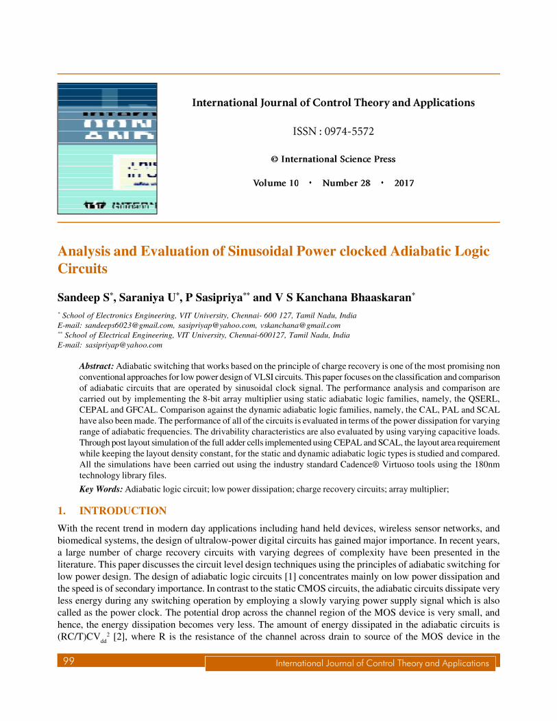
Fig. 1 shows the structure of static adiabatic inverter circuits namely, QSERL, CEPAL and GFCAL. All thestatic adiabatic inverters have a single rail output. The static adiabatic circuits employ diodes to maintain theoutput constant and the major advantage of these adiabatic circuits is the reduction in the switching power loss.However, the presence of the diodes results in the knee or cut-in voltage drop across the diodes and hence, theoutput voltage does not swing enough to reach the power clock peak value.
The QSERL being the preliminary version of static adiabatic logic was developed by Kaushik Roy [7]. Thestructure of QSERL is derived from the static CMOS logic inverter which is provided with two additional diodesconnected in the pull up and pull down path. The structure employs two complementary sinusoidal power clocksignals. On the other hand, the CEPAL is derived from the QSERL with two diodes in the charging path andanother set of two diodes in the discharging path. The presence of the additional diodes is to ensure the eliminationof the floating node output during the hold phase of adiabatic operation, and hence it is identified as the singlephase static adiabatic logic. Hence, the throughput of the CEPAL is twice that of the QSERL. The GFCAL isalso derived from the QSERL structure by replacing the complementary sinusoidal power supply with a singlesinusoidal power clock signal. The GFCAL gates connected in cascade uses the same power supply clock signaland it is also called as single phase static adiabatic circuit.
101 International Journal of Control Theory and Applications
Analysis and Evaluation of Sinusoidal Power clocked Adiabatic Logic Circuits
Dynamic Adiabatic Circuits
Figure 1: Static Adiabatic Inverters a) QSERL, b) CEPAL and c) GFCAL
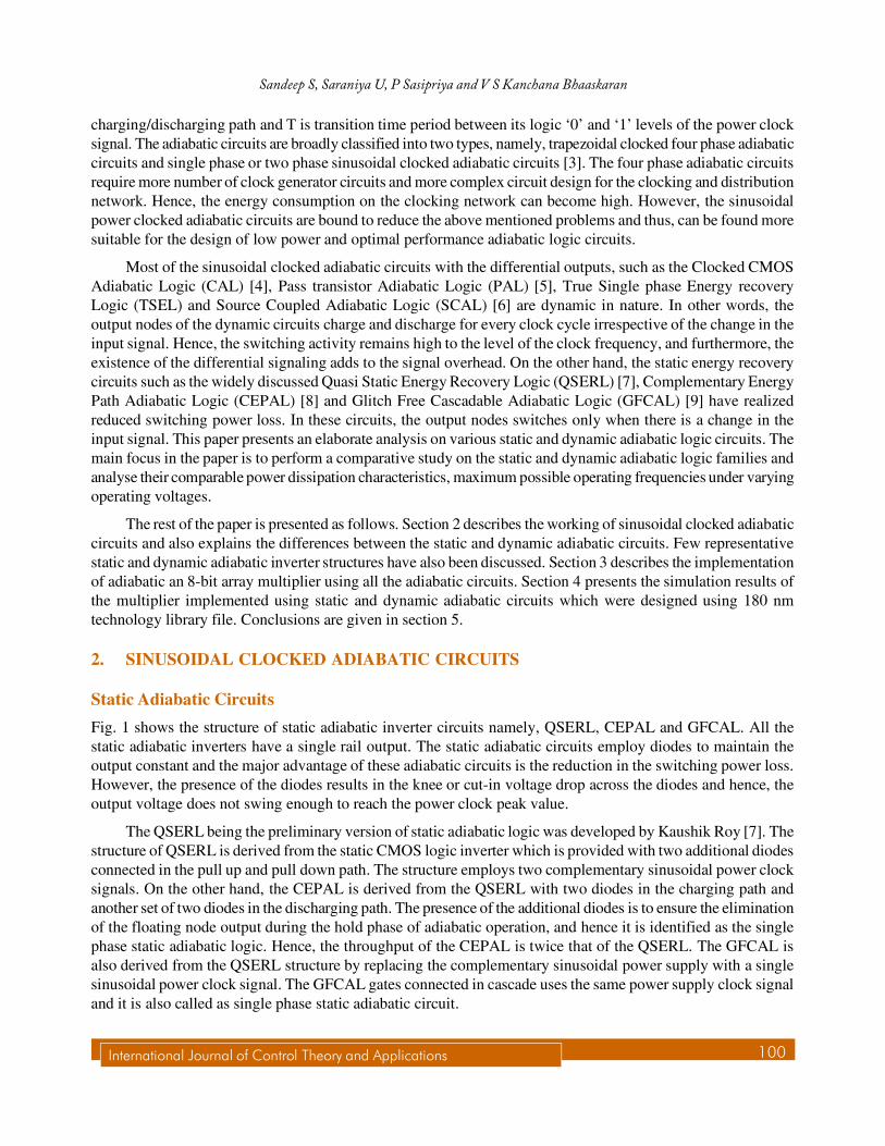
Figure 2: Dynamic Adiabatic Inverters a) CAL, b) PAL, c) SCAL- NMOS and d) SCAL – PMOS
International Journal of Control Theory and Applications 102
Sandeep S, Saraniya U, P Sasipriya and V S Kanchana Bhaaskaran
Fig. 2 shows the transistor based schematic of dynamic adiabatic circuit inverters/buffers, namely, CAL,PAL and SCAL. The dynamic adiabatic circuits have differential signaling, i.e., both the inputs and outputs areavailable in its standard and in its complementary form. All these dynamic adiabatic circuits have their functionaland complementary functional blocks, which are connected to the sense amplifier. The outputs (out and outbar)are taken out from the sense amplifier.
CAL is derived from efficient charge recovery logic ECRL [10] with an additional transistor for controllingits phase of operation. The CAL is a single phase dynamic adiabatic circuit which employs sinusoidal powerclock signal and an auxiliary clock signal source. CAL uses complementary auxiliary clock signal for its cascadedstages of pipelining operation. The auxiliary clock can be derived from the sinusoidal clock signal by usingfrequency divider circuit. PAL is a single phase dynamic adiabatic circuit which is similar to the ECRL instructure with modification in the power supply connection. The output node goes into high impedance statewhen the output node is logic ‘0’. The PAL uses two complementary sinusoidal power clock signal for itscascaded operation. SCAL is a single phase dynamic adiabatic circuit which employs NMOS and PMOS logicstructure. The NMOS and PMOS gates are connected in cascade for its multistage complex network. In contrastto other dynamic circuits, the SCAL uses current source transistor along with the functional block and senseamplifier. The sizing of the current source transistor plays an important role in the power dissipation of the logiccircuits designed using SCAL.
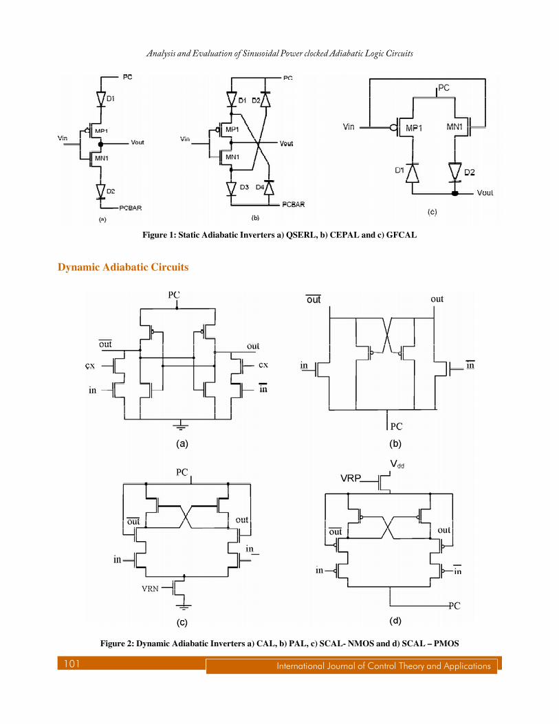
Fig. 3 shows the input and output (I/O) waveforms of the static and dynamic adiabatic inverters. Staticadiabatic inverters are similar to the static CMOS inverter having single rail inverted output. The output nodedoes not switch for every cycle and the change is reflected only when there is a change in the input signal duringevaluation phase of the power clock signal.
Figure 3: I/O Waveforms of adiabatic Inverters a) I/O of Waveform for Static inverter, b) Power clock andc) I/O Waveform for Dynamic inverter
103 International Journal of Control Theory and Applications
Analysis and Evaluation of Sinusoidal Power clocked Adiabatic Logic Circuits
Dynamic inverters have dual rail complementary output. Based on the input and its complementary signals,either the normal or complementary output at the output nodes follows the power clock during the evaluationphase of the power clock signal.
3. STRUCTURE AND DESIGN OF AN ADIABATIC MULTIPLIER
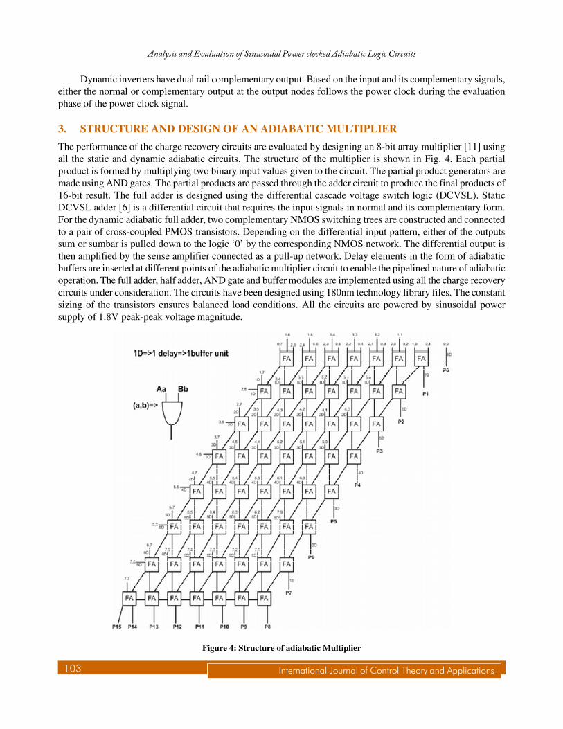
The performance of the charge recovery circuits are evaluated by designing an 8-bit array multiplier [11] usingall the static and dynamic adiabatic circuits. The structure of the multiplier is shown in Fig. 4. Each partialproduct is formed by multiplying two binary input values given to the circuit. The partial product generators aremade using AND gates. The partial products are passed through the adder circuit to produce the final products of16-bit result. The full adder is designed using the differential cascade voltage switch logic (DCVSL). StaticDCVSL adder [6] is a differential circuit that requires the input signals in normal and its complementary form.For the dynamic adiabatic full adder, two complementary NMOS switching trees are constructed and connectedto a pair of cross-coupled PMOS transistors. Depending on the differential input pattern, either of the outputssum or sumbar is pulled down to the logic ‘0’ by the corresponding NMOS network. The differential output isthen amplified by the sense amplifier connected as a pull-up network. Delay elements in the form of adiabaticbuffers are inserted at different points of the adiabatic multiplier circuit to enable the pipelined nature of adiabaticoperation. The full adder, half adder, AND gate and buffer modules are implemented using all the charge recoverycircuits under consideration. The circuits have been designed using 180nm technology library files. The constantsizing of the transistors ensures balanced load conditions. All the circuits are powered by sinusoidal powersupply of 1.8V peak-peak voltage magnitude.
Figure 4: Structure of adiabatic Multiplier
International Journal of Control Theory and Applications 104
Sandeep S, Saraniya U, P Sasipriya and V S Kanchana Bhaaskaran
4. RESULTS AND DISCUSSION
The 8-bit array multiplier has been employed as a benchmark circuit for validating the comparative performanceanalyses of all the charge recovery circuits. The performance of the circuits is evaluated through powerconsumption comparison at various power-clock frequency values. The drivability is also studied for differentcapacitive loads to identify the drivability characteristics and the adiabatic efficiency. The average powerconsumption incurred by the circuits is extracted from the transient simulations carried out using CADENCE®EDA tools, by integrating the power over the period of simulation. The power consumption of the clock generatorcircuit is considered negligible.
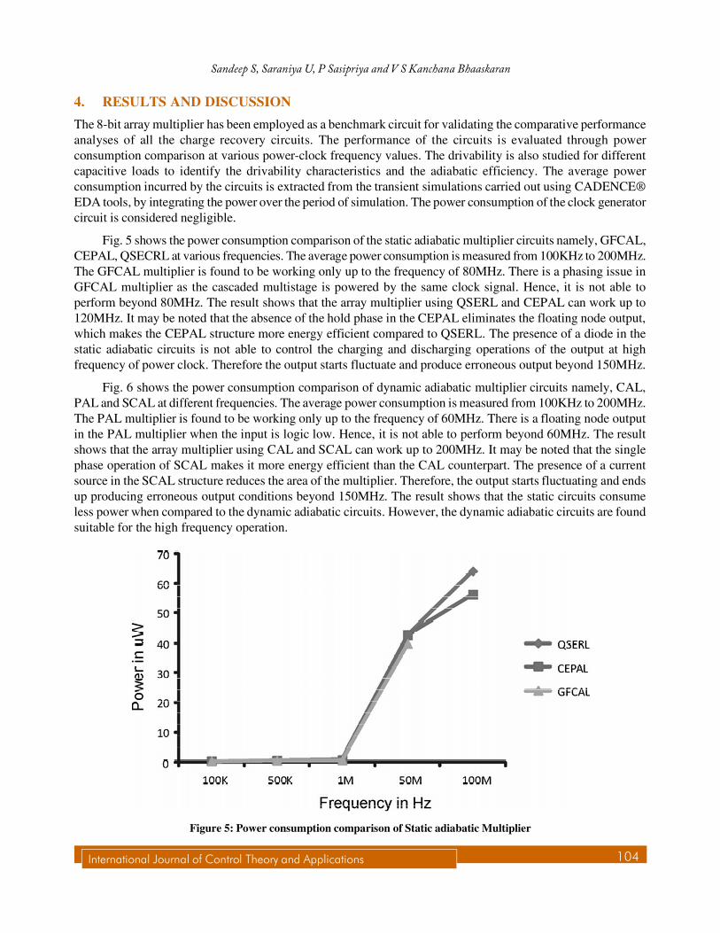
Fig. 5 shows the power consumption comparison of the static adiabatic multiplier circuits namely, GFCAL,CEPAL, QSECRL at various frequencies. The average power consumption is measured from 100KHz to 200MHz.The GFCAL multiplier is found to be working only up to the frequency of 80MHz. There is a phasing issue inGFCAL multiplier as the cascaded multistage is powered by the same clock signal. Hence, it is not able toperform beyond 80MHz. The result shows that the array multiplier using QSERL and CEPAL can work up to120MHz. It may be noted that the absence of the hold phase in the CEPAL eliminates the floating node output,which makes the CEPAL structure more energy efficient compared to QSERL. The presence of a diode in thestatic adiabatic circuits is not able to control the charging and discharging operations of the output at highfrequency of power clock. Therefore the output starts fluctuate and produce erroneous output beyond 150MHz.
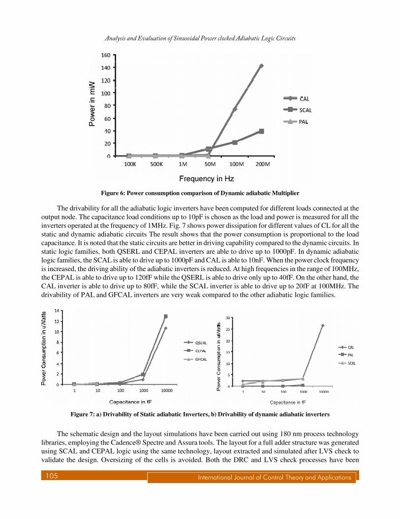
Fig. 6 shows the power consumption comparison of dynamic adiabatic multiplier circuits namely, CAL,PAL and SCAL at different frequencies. The average power consumption is measured from 100KHz to 200MHz.The PAL multiplier is found to be working only up to the frequency of 60MHz. There is a floating node outputin the PAL multiplier when the input is logic low. Hence, it is not able to perform beyond 60MHz. The resultshows that the array multiplier using CAL and SCAL can work up to 200MHz. It may be noted that the singlephase operation of SCAL makes it more energy efficient than the CAL counterpart. The presence of a currentsource in the SCAL structure reduces the area of the multiplier. Therefore, the output starts fluctuating and endsup producing erroneous output conditions beyond 150MHz. The result shows that the static circuits consumeless power when compared to the dynamic adiabatic circuits. However, the dynamic adiabatic circuits are foundsuitable for the high frequency operation.
Figure 5: Power consumption comparison of Static adiabatic Multiplier
105 International Journal of Control Theory and Applications
Analysis and Evaluation of Sinusoidal Power clocked Adiabatic Logic Circuits
Figure 6: Power consumption comparison of Dynamic adiabatic Multiplier
The drivability for all the adiabatic logic inverters have been computed for different loads connected at theoutput node. The capacitance load conditions up to 10pF is chosen as the load and power is measured for all theinverters operated at the frequency of 1MHz. Fig. 7 shows power dissipation for different values of CL for all thestatic and dynamic adiabatic circuits The result shows that the power consumption is proportional to the loadcapacitance. It is noted that the static circuits are better in driving capability compared to the dynamic circuits. Instatic logic families, both QSERL and CEPAL inverters are able to drive up to 1000pF. In dynamic adiabaticlogic families, the SCAL is able to drive up to 1000pF and CAL is able to 10nF. When the power clock frequencyis increased, the driving ability of the adiabatic inverters is reduced. At high frequencies in the range of 100MHz,the CEPAL is able to drive up to 120fF while the QSERL is able to drive only up to 40fF. On the other hand, theCAL inverter is able to drive up to 80fF, while the SCAL inverter is able to drive up to 20fF at 100MHz. Thedrivability of PAL and GFCAL inverters are very weak compared to the other adiabatic logic families.
Figure 7: a) Drivability of Static adiabatic Inverters, b) Drivability of dynamic adiabatic inverters
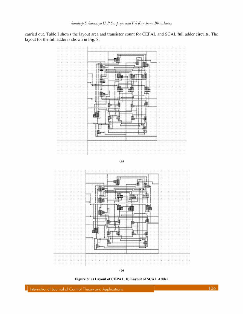
The schematic design and the layout simulations have been carried out using 180 nm process technologylibraries, employing the Cadence® Spectre and Assura tools. The layout for a full adder structure was generatedusing SCAL and CEPAL logic using the same technology, layout extracted and simulated after LVS check tovalidate the design. Oversizing of the cells is avoided. Both the DRC and LVS check processes have been
International Journal of Control Theory and Applications 106
Sandeep S, Saraniya U, P Sasipriya and V S Kanchana Bhaaskaran
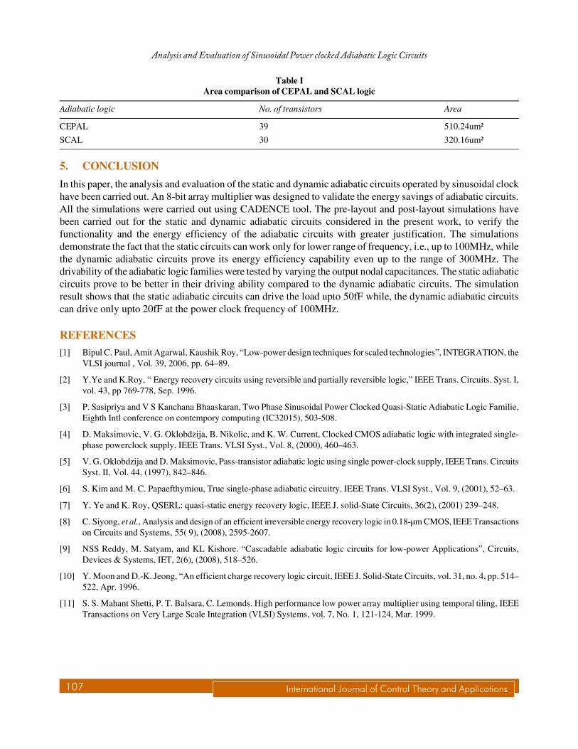
carried out. Table I shows the layout area and transistor count for CEPAL and SCAL full adder circuits. Thelayout for the full adder is shown in Fig. 8.
Figure 8: a) Layout of CEPAL, b) Layout of SCAL Adder
(a)
(b)
107 International Journal of Control Theory and Applications
Analysis and Evaluation of Sinusoidal Power clocked Adiabatic Logic Circuits
Table IArea comparison of CEPAL and SCAL logic
Adiabatic logic No. of transistors Area
CEPAL 39 510.24um²
SCAL 30 320.16um²
5. CONCLUSION
In this paper, the analysis and evaluation of the static and dynamic adiabatic circuits operated by sinusoidal clockhave been carried out. An 8-bit array multiplier was designed to validate the energy savings of adiabatic circuits.All the simulations were carried out using CADENCE tool. The pre-layout and post-layout simulations havebeen carried out for the static and dynamic adiabatic circuits considered in the present work, to verify thefunctionality and the energy efficiency of the adiabatic circuits with greater justification. The simulationsdemonstrate the fact that the static circuits can work only for lower range of frequency, i.e., up to 100MHz, whilethe dynamic adiabatic circuits prove its energy efficiency capability even up to the range of 300MHz. Thedrivability of the adiabatic logic families were tested by varying the output nodal capacitances. The static adiabaticcircuits prove to be better in their driving ability compared to the dynamic adiabatic circuits. The simulationresult shows that the static adiabatic circuits can drive the load upto 50fF while, the dynamic adiabatic circuitscan drive only upto 20fF at the power clock frequency of 100MHz.
REFERENCES
[1] Bipul C. Paul, Amit Agarwal, Kaushik Roy, “Low-power design techniques for scaled technologies”, INTEGRATION, theVLSI journal , Vol. 39, 2006, pp. 64–89.
[2] Y.Ye and K.Roy, “ Energy recovery circuits using reversible and partially reversible logic,” IEEE Trans. Circuits. Syst. I,vol. 43, pp 769-778, Sep. 1996.
[3] P. Sasipriya and V S Kanchana Bhaaskaran, Two Phase Sinusoidal Power Clocked Quasi-Static Adiabatic Logic Familie,Eighth Intl conference on contempory computing (IC32015), 503-508.
[4] D. Maksimovic, V. G. Oklobdzija, B. Nikolic, and K. W. Current, Clocked CMOS adiabatic logic with integrated single-phase powerclock supply, IEEE Trans. VLSI Syst., Vol. 8, (2000), 460–463.
[5] V. G. Oklobdzija and D. Maksimovic, Pass-transistor adiabatic logic using single power-clock supply, IEEE Trans. CircuitsSyst. II, Vol. 44, (1997), 842–846.
[6] S. Kim and M. C. Papaefthymiou, True single-phase adiabatic circuitry, IEEE Trans. VLSI Syst., Vol. 9, (2001), 52–63.
[7] Y. Ye and K. Roy, QSERL: quasi-static energy recovery logic, IEEE J. solid-State Circuits, 36(2), (2001) 239–248.
[8] C. Siyong, et al., Analysis and design of an efficient irreversible energy recovery logic in 0.18-µm CMOS, IEEE Transactionson Circuits and Systems, 55( 9), (2008), 2595-2607.
[9] NSS Reddy, M. Satyam, and KL Kishore. “Cascadable adiabatic logic circuits for low-power Applications”, Circuits,Devices & Systems, IET, 2(6), (2008), 518–526.
[10] Y. Moon and D.-K. Jeong, “An efficient charge recovery logic circuit, IEEE J. Solid-State Circuits, vol. 31, no. 4, pp. 514–522, Apr. 1996.
[11] S. S. Mahant Shetti, P. T. Balsara, C. Lemonds. High performance low power array multiplier using temporal tiling, IEEETransactions on Very Large Scale Integration (VLSI) Systems, vol. 7, No. 1, 121-124, Mar. 1999.