Embed Size (px)
Citation preview
Application Note 92
AN92-1
Bias Voltage and Current Sense Circuits forAvalanche PhotodiodesFeeding and Reading the APD
Jim Williams, Linear Technology Corporation
November 2002
INTRODUCTION
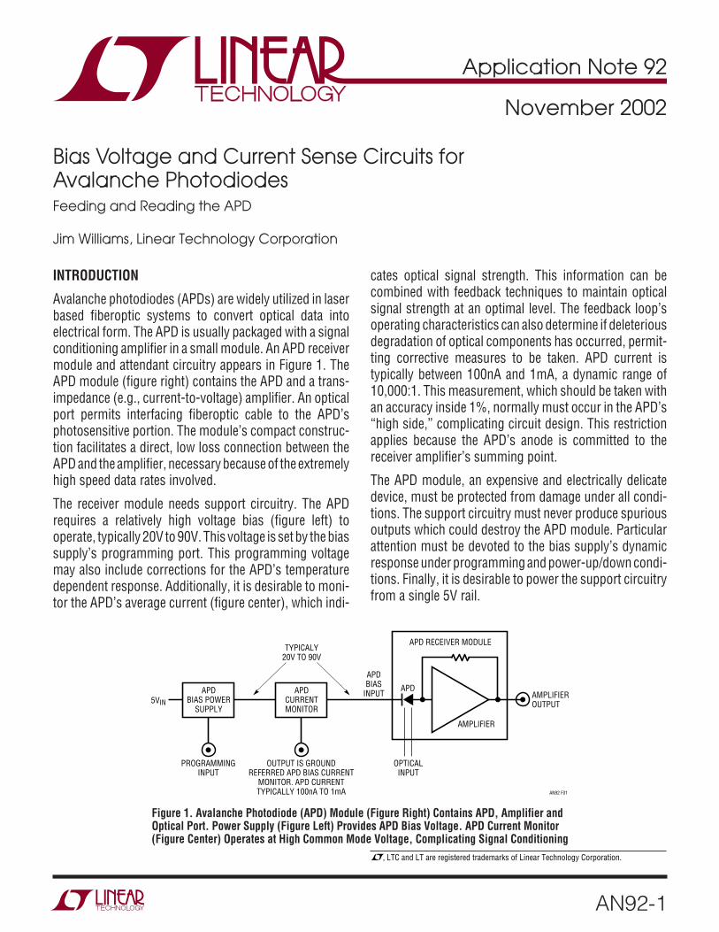
Avalanche photodiodes (APDs) are widely utilized in laserbased fiberoptic systems to convert optical data intoelectrical form. The APD is usually packaged with a signalconditioning amplifier in a small module. An APD receivermodule and attendant circuitry appears in Figure 1. TheAPD module (figure right) contains the APD and a trans-impedance (e.g., current-to-voltage) amplifier. An opticalport permits interfacing fiberoptic cable to the APD’sphotosensitive portion. The module’s compact construc-tion facilitates a direct, low loss connection between theAPD and the amplifier, necessary because of the extremelyhigh speed data rates involved.
The receiver module needs support circuitry. The APDrequires a relatively high voltage bias (figure left) tooperate, typically 20V to 90V. This voltage is set by the biassupply’s programming port. This programming voltagemay also include corrections for the APD’s temperaturedependent response. Additionally, it is desirable to moni-tor the APD’s average current (figure center), which indi-
, LTC and LT are registered trademarks of Linear Technology Corporation.
cates optical signal strength. This information can becombined with feedback techniques to maintain opticalsignal strength at an optimal level. The feedback loop’soperating characteristics can also determine if deleteriousdegradation of optical components has occurred, permit-ting corrective measures to be taken. APD current istypically between 100nA and 1mA, a dynamic range of10,000:1. This measurement, which should be taken withan accuracy inside 1%, normally must occur in the APD’s“high side,” complicating circuit design. This restrictionapplies because the APD’s anode is committed to thereceiver amplifier’s summing point.
The APD module, an expensive and electrically delicatedevice, must be protected from damage under all condi-tions. The support circuitry must never produce spuriousoutputs which could destroy the APD module. Particularattention must be devoted to the bias supply’s dynamicresponse under programming and power-up/down condi-tions. Finally, it is desirable to power the support circuitryfrom a single 5V rail.
AMPLIFIEROUTPUT
APD RECEIVER MODULE
APDBIAS
INPUT
TYPICALY20V TO 90V
AMPLIFIER
OUTPUT IS GROUNDREFERRED APD BIAS CURRENT
MONITOR. APD CURRENTTYPICALLY 100nA TO 1mA
OPTICALINPUT
APDAPDCURRENTMONITOR
PROGRAMMINGINPUT
5VIN
AN92 F01
APDBIAS POWER
SUPPLY
Figure 1. Avalanche Photodiode (APD) Module (Figure Right) Contains APD, Amplifier andOptical Port. Power Supply (Figure Left) Provides APD Bias Voltage. APD Current Monitor(Figure Center) Operates at High Common Mode Voltage, Complicating Signal Conditioning
Application Note 92
AN92-2
The bias voltage and current measurement requirementsdescribed above constitute a significant design challengeand are addressed in the following text.
Simple Current Monitor Circuits (with Problems)
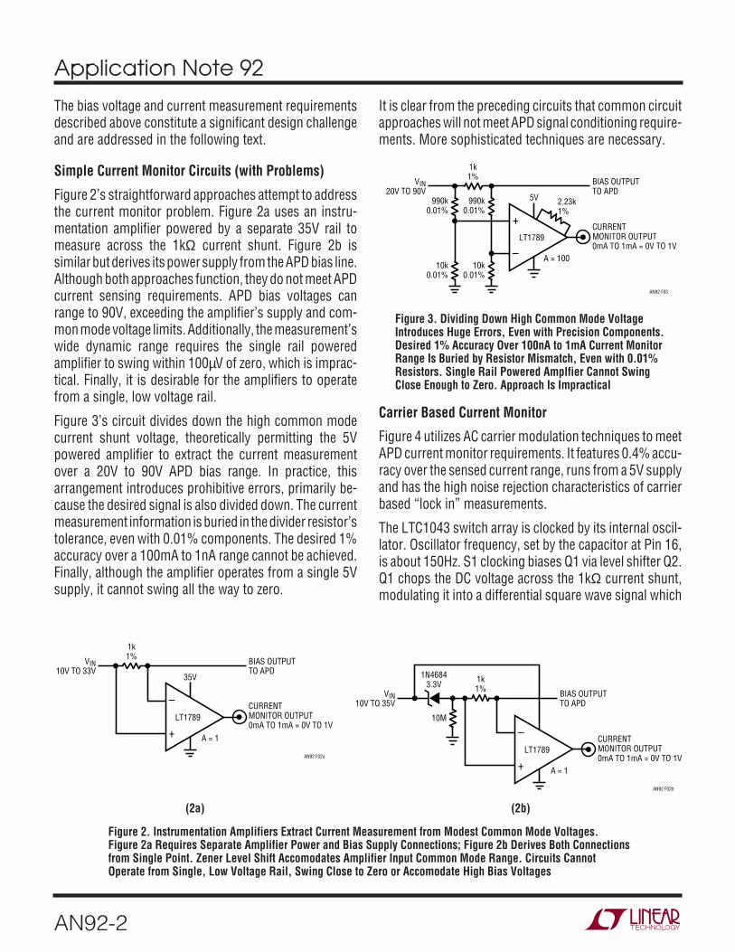
Figure 2’s straightforward approaches attempt to addressthe current monitor problem. Figure 2a uses an instru-mentation amplifier powered by a separate 35V rail tomeasure across the 1kΩ current shunt. Figure 2b issimilar but derives its power supply from the APD bias line.Although both approaches function, they do not meet APDcurrent sensing requirements. APD bias voltages canrange to 90V, exceeding the amplifier’s supply and com-mon mode voltage limits. Additionally, the measurement’swide dynamic range requires the single rail poweredamplifier to swing within 100µV of zero, which is imprac-tical. Finally, it is desirable for the amplifiers to operatefrom a single, low voltage rail.
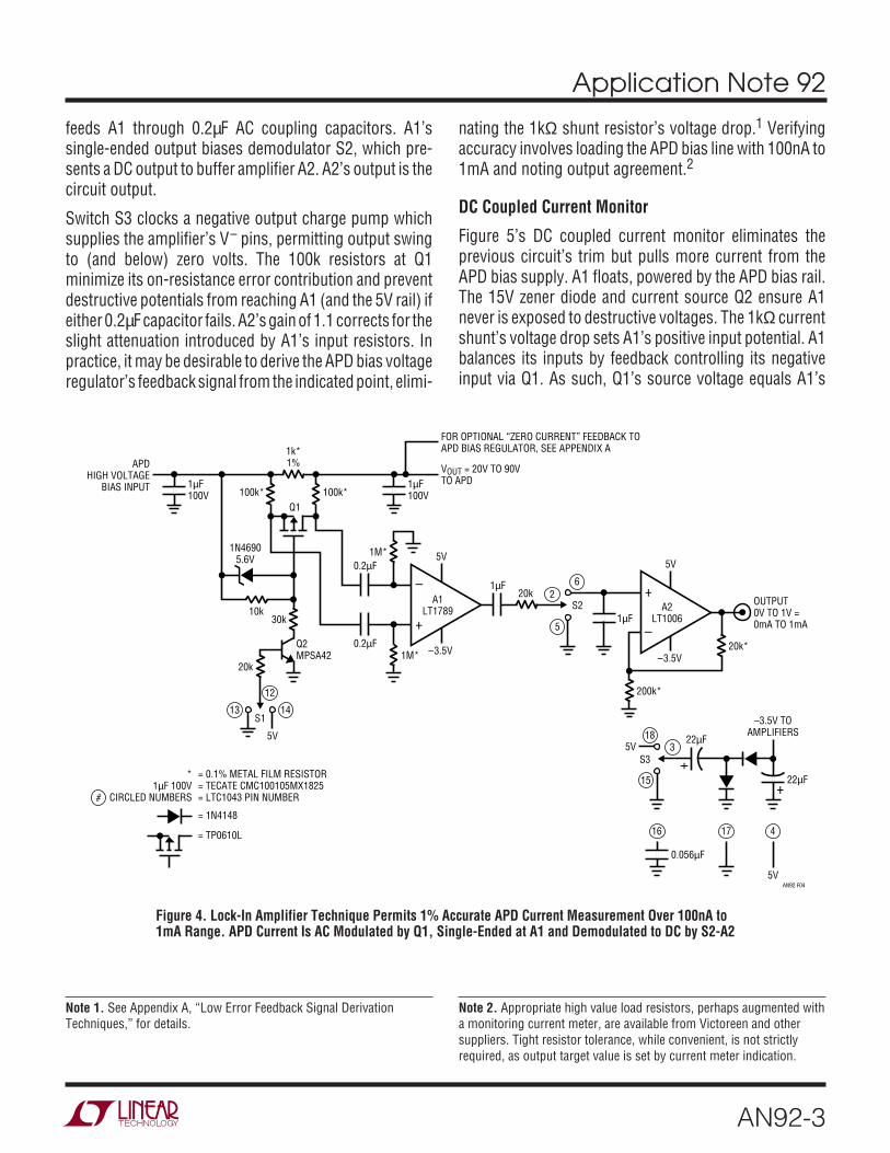
Figure 3’s circuit divides down the high common modecurrent shunt voltage, theoretically permitting the 5Vpowered amplifier to extract the current measurementover a 20V to 90V APD bias range. In practice, thisarrangement introduces prohibitive errors, primarily be-cause the desired signal is also divided down. The currentmeasurement information is buried in the divider resistor’stolerance, even with 0.01% components. The desired 1%accuracy over a 100mA to 1nA range cannot be achieved.Finally, although the amplifier operates from a single 5Vsupply, it cannot swing all the way to zero.
It is clear from the preceding circuits that common circuitapproaches will not meet APD signal conditioning require-ments. More sophisticated techniques are necessary.
CURRENT MONITOR OUTPUT0mA TO 1mA = 0V TO 1V
+
–
35V
LT1789
A = 1
BIAS OUTPUTTO APD
VIN10V TO 33V
AN92 F02a
1k1%
CURRENT MONITOR OUTPUT0mA TO 1mA = 0V TO 1V
+
–LT1789
A = 1
BIAS OUTPUTTO APD
VIN10V TO 35V
1N46843.3V
AN92 F02b
1k1%
10M
Figure 2. Instrumentation Amplifiers Extract Current Measurement from Modest Common Mode Voltages.Figure 2a Requires Separate Amplifier Power and Bias Supply Connections; Figure 2b Derives Both Connectionsfrom Single Point. Zener Level Shift Accomodates Amplifier Input Common Mode Range. Circuits CannotOperate from Single, Low Voltage Rail, Swing Close to Zero or Accomodate High Bias Voltages
(2a) (2b)
CURRENTMONITOR OUTPUT0mA TO 1mA = 0V TO 1V
–
+
5V
LT1789
A = 100
BIAS OUTPUTTO APD
VIN20V TO 90V
AN92 F03
1k1%
990k0.01%
990k0.01%
10k0.01%
10k0.01%
2.23k1%
Figure 3. Dividing Down High Common Mode VoltageIntroduces Huge Errors, Even with Precision Components.Desired 1% Accuracy Over 100nA to 1mA Current MonitorRange Is Buried by Resistor Mismatch, Even with 0.01%Resistors. Single Rail Powered Amplfier Cannot SwingClose Enough to Zero. Approach Is Impractical
Carrier Based Current Monitor
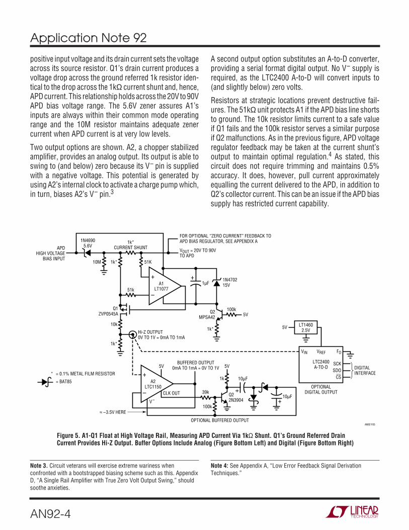
Figure 4 utilizes AC carrier modulation techniques to meetAPD current monitor requirements. It features 0.4% accu-racy over the sensed current range, runs from a 5V supplyand has the high noise rejection characteristics of carrierbased “lock in” measurements.
The LTC1043 switch array is clocked by its internal oscil-lator. Oscillator frequency, set by the capacitor at Pin 16,is about 150Hz. S1 clocking biases Q1 via level shifter Q2.Q1 chops the DC voltage across the 1kΩ current shunt,modulating it into a differential square wave signal which
Application Note 92
AN92-3
feeds A1 through 0.2µF AC coupling capacitors. A1’ssingle-ended output biases demodulator S2, which pre-sents a DC output to buffer amplifier A2. A2’s output is thecircuit output.
Switch S3 clocks a negative output charge pump whichsupplies the amplifier’s V– pins, permitting output swingto (and below) zero volts. The 100k resistors at Q1minimize its on-resistance error contribution and preventdestructive potentials from reaching A1 (and the 5V rail) ifeither 0.2µF capacitor fails. A2’s gain of 1.1 corrects for theslight attenuation introduced by A1’s input resistors. Inpractice, it may be desirable to derive the APD bias voltageregulator’s feedback signal from the indicated point, elimi-
nating the 1kΩ shunt resistor’s voltage drop.1 Verifyingaccuracy involves loading the APD bias line with 100nA to1mA and noting output agreement.2
DC Coupled Current Monitor
Figure 5’s DC coupled current monitor eliminates theprevious circuit’s trim but pulls more current from theAPD bias supply. A1 floats, powered by the APD bias rail.The 15V zener diode and current source Q2 ensure A1never is exposed to destructive voltages. The 1kΩ currentshunt’s voltage drop sets A1’s positive input potential. A1balances its inputs by feedback controlling its negativeinput via Q1. As such, Q1’s source voltage equals A1’s
OUTPUT0V TO 1V = 0mA TO 1mA
5V
+
–
5V
A1LT1789
–3.5V0.2µF
S1
0.2µF
VOUT = 20V TO 90VTO APD
FOR OPTIONAL “ZERO CURRENT” FEEDBACK TOAPD BIAS REGULATOR, SEE APPENDIX A
APDHIGH VOLTAGE
BIAS INPUT
AN92 F04
1k*1%
100k*
–
+
5V
A2LT1006
–3.5V
100k*Q1
1M*
1M*Q2MPSA42
5VS3
S2
20k
15
16 17 4
318
5
26
12
13 14
22µF
22µF
–3.5V TOAMPLIFIERS
0.056µF
5V
20k*
20k
200k*
1µF
1µF
1µF100V
1µF100V
30k10k
1N46905.6V
#
= 1N4148
= 0.1% METAL FILM RESISTOR= TECATE CMC100105MX1825= LTC1043 PIN NUMBER
= TP0610L
*1µF 100V
CIRCLED NUMBERS
+
+
Figure 4. Lock-In Amplifier Technique Permits 1% Accurate APD Current Measurement Over 100nA to1mA Range. APD Current Is AC Modulated by Q1, Single-Ended at A1 and Demodulated to DC by S2-A2
Note 1. See Appendix A, “Low Error Feedback Signal DerivationTechniques,” for details.
Note 2. Appropriate high value load resistors, perhaps augmented witha monitoring current meter, are available from Victoreen and othersuppliers. Tight resistor tolerance, while convenient, is not strictlyrequired, as output target value is set by current meter indication.
Application Note 92
AN92-4
positive input voltage and its drain current sets the voltageacross its source resistor. Q1’s drain current produces avoltage drop across the ground referred 1k resistor iden-tical to the drop across the 1kΩ current shunt and, hence,APD current. This relationship holds across the 20V to 90VAPD bias voltage range. The 5.6V zener assures A1’sinputs are always within their common mode operatingrange and the 10M resistor maintains adequate zenercurrent when APD current is at very low levels.
Two output options are shown. A2, a chopper stabilizedamplifier, provides an analog output. Its output is able toswing to (and below) zero because its V– pin is suppliedwith a negative voltage. This potential is generated byusing A2’s internal clock to activate a charge pump which,in turn, biases A2’s V– pin.3
A second output option substitutes an A-to-D converter,providing a serial format digital output. No V– supply isrequired, as the LTC2400 A-to-D will convert inputs to(and slightly below) zero volts.
Resistors at strategic locations prevent destructive fail-ures. The 51kΩ unit protects A1 if the APD bias line shortsto ground. The 10k resistor limits current to a safe valueif Q1 fails and the 100k resistor serves a similar purposeif Q2 malfunctions. As in the previous figure, APD voltageregulator feedback may be taken at the current shunt’soutput to maintain optimal regulation.4 As stated, thiscircuit does not require trimming and maintains 0.5%accuracy. It does, however, pull current approximatelyequalling the current delivered to the APD, in addition toQ2’s collector current. This can be an issue if the APD biassupply has restricted current capability.
Hi-Z OUTPUT0V TO 1V = 0mA TO 1mA
–
+A1
LT1077
VOUT = 20V TO 90VTO APD
APDHIGH VOLTAGE
BIAS INPUT
AN92 F05
1k*CURRENT SHUNT
1k*
–
+A2
LTC1150CLK OUT
BUFFERED OUTPUT0mA TO 1mA = 0V TO 1V5V
V –
≈ –3.5V HERE
51k
10k
1k*
1k*
51K
Q2MPSA42
Q22N3904
10µF
10µF
Q1ZVP0545A
100k
39k
1k
5V
1µF
= BAT85
= 0.1% METAL FILM RESISTOR*
10M
1N46905.6V
1N470215V
5V
5V
100k
VIN VREF
LTC2400A-TO-D
OPTIONALDIGITAL OUTPUT
OPTIONAL BUFFERED OUTPUT
FO
SCKDIGITALINTERFACESDO
CS
LT14602.5V
+
+
+FOR OPTIONAL “ZERO CURRENT” FEEDBACK TOAPD BIAS REGULATOR, SEE APPENDIX A
Figure 5. A1-Q1 Float at High Voltage Rail, Measuring APD Current Via 1kΩ Shunt. Q1’s Ground Referred DrainCurrent Provides Hi-Z Output. Buffer Options Include Analog (Figure Bottom Left) and Digital (Figure Bottom Right)
Note 3. Circuit veterans will exercise extreme wariness whenconfronted with a bootstrapped biasing scheme such as this. AppendixD, “A Single Rail Amplifier with True Zero Volt Output Swing,” shouldsoothe anxieties.
Note 4: See Appendix A, “Low Error Feedback Signal DerivationTechniques.”
Application Note 92
AN92-5
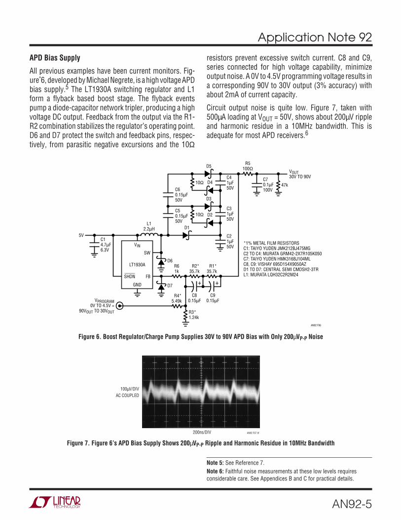
APD Bias Supply
All previous examples have been current monitors. Fig-ure 6, developed by Michael Negrete, is a high voltage APDbias supply.5 The LT1930A switching regulator and L1form a flyback based boost stage. The flyback eventspump a diode-capacitor network tripler, producing a highvoltage DC output. Feedback from the output via the R1-R2 combination stabilizes the regulator’s operating point.D6 and D7 protect the switch and feedback pins, respec-tively, from parasitic negative excursions and the 10Ω
resistors prevent excessive switch current. C8 and C9,series connected for high voltage capability, minimizeoutput noise. A 0V to 4.5V programming voltage results ina corresponding 90V to 30V output (3% accuracy) withabout 2mA of current capacity.
Circuit output noise is quite low. Figure 7, taken with500µA loading at VOUT = 50V, shows about 200µV rippleand harmonic residue in a 10MHz bandwidth. This isadequate for most APD receivers.6
VIN
L12.2µH
SW
R61k
R4*5.49k
R3*1.24k
*1% METAL FILM RESISTORSC1: TAIYO YUDEN JMK212BJ475MGC2 TO C4: MURATA GRM42-2X7R105K050C7: TAIYO YUDEN HMK316BJ104MLC8, C9: VISHAY 695D154X9050AZD1 TO D7: CENTRAL SEMI CMDSH2-3TRL1: MURATA LQH32C2R2M24
R2*35.7k
R1*35.7k
C80.15µF
C60.15µF50V
C21µF50V
C31µF50V
C41µF50V
C70.1µF100V
47k
C50.15µF50V
VPROGRAM0V TO 4.5V =
90VOUT TO 30VOUT
C90.15µF
LT1930A
FBSHDN
AN92 F06
D6
D1
D3
D2
D4
C14.7µF6.3V
5V
D7GND
D5
10Ω
10Ω
R5100Ω VOUT
30V TO 90V
+ +
Figure 6. Boost Regulator/Charge Pump Supplies 30V to 90V APD Bias with Only 200µVP-P Noise
Figure 7. Figure 6’s APD Bias Supply Shows 200µVP-P Ripple and Harmonic Residue in 10MHz Bandwidth
200ns/DIV AN92 F07.tif
100µV/DIVAC COUPLED
Note 5: See Reference 7.Note 6: Faithful noise measurements at these low levels requiresconsiderable care. See Appendices B and C for practical details.
Application Note 92
AN92-6
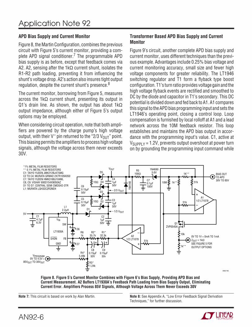
APD Bias Supply and Current Monitor
Figure 8, the Martin Configuration, combines the previouscircuit with Figure 5’s current monitor, providing a com-plete APD signal conditioner.7 The programmable APDbias supply is as before, except that feedback comes viaA2. A2, sensing after the 1kΩ current shunt, isolates theR1-R2 path loading, preventing it from influencing theshunt’s voltage drop. A2’s action also insures tight outputregulation, despite the current shunt’s presence.8
The current monitor, borrowing from Figure 5, measuresacross the 1kΩ current shunt, presenting its output inQ1’s drain line. As shown, the output has about 1kΩoutput impedance, although either of Figure 5’s outputoptions may be employed.
When considering circuit operation, note that both ampli-fiers are powered by the charge pump’s high voltageoutput, with their V– pin returned to the “2/3 VOUT” point.This biasing permits the amplifiers to process high voltagesignals, although the voltage across them never exceeds30V.
Transformer Based APD Bias Supply and CurrentMonitor
Figure 9’s circuit, another complete APD bias supply andcurrent monitor, uses different techniques than the previ-ous example. Advantages include 0.25% bias voltage andcurrent monitoring accuracy, small size and fewer highvoltage components for greater reliability. The LT1946switching regulator and T1 form a flyback type boostconfiguration. T1’s turn ratio provides voltage gain and thehigh voltage flyback events are rectified and smoothed toDC by the diode and capacitor in T1’s secondary. This DCpotential is divided down and fed back to A1. A1 comparesthis signal to the APD bias programming input and sets theLT1946’s operating point, closing a control loop. Loopcompensation is furnished by local rolloff at A1 and a leadnetwork across the 10M feedback resistor. This loopestablishes and maintains the APD bias output in accor-dance with the programming input’s value. C1, active atVSUPPLY = 1.2V, prevents output overshoot at power turnon by grounding the programming input command while
BIAS OUT TO APD30V TO 85V
VIN
L12.2µH
SW
R61k
R4*5.49k
R3*1.24k
*1% METAL FILM RESISTORS** 0.1% METAL FILM RESISTORSC1: TAIYO YUDEN JMK212BJ475MGC2 TO C4: MURATA GRM42-2X7R105K050C7: TAIYO YUDEN HMK316BJ104MLC8, C9: VISHAY 695D154X9050AZD1 TO D7: CENTRAL SEMI CMDSH2-3TRL1: MURATA LQH32C2R2M24
R2*35.7k
R1*32.3k
51k
C80.15µF
50V
C60.15µF50V
C21µF50V
C31µF50V
1/3 VOUT
VOUT
C41µF50V
C70.1µF100V
C50.15µF50V
VPROGRAM0V TO 4.5V =
85VOUT TO 30VOUT
0V TO 1V = 0mA TO 1mAZOUT ≈ 1kΩSEE FIGURE 5 FOR OUTPUT OPTIONS
C90.15µF
50v
LT1930A
FBSHDN
AN92 F06
D6
D1
D3
D2
D4
C14.7µF6.3V
5V
D7GND
D5
10Ω
10Ω
R5100Ω 1K**
1N46905.6V
1N41
48
+ +
–
+
+
–
51k
10k
1k**
1k**10M
A21/2 LT1078
A11/2 LT1078
Q1ZVP0545A
51k
2/3 VOUT
Figure 8. Figure 5’s Current Monitor Combines with Figure 6’s Bias Supply, Providing APD Bias andCurrent Measurement. A2 Buffers LT1930A’s Feedback Path Loading from Bias Supply Output, EliminatingCurrent Error. Amplifiers Process 85V Signals, Although Voltage Across Them Never Exceeds 30V
Note 7: This circuit is based on work by Alan Martin. Note 8: See Appendix A, “Low Error Feedback Signal DerivationTechniques,” for further discussion.

Application Note 92
AN92-7
simultaneously forcing A1’s output low. This shuts off theswitching regulator and no high voltage is produced.When power at turn on reaches ≈4V, C1 changes state andA1’s positive input ramps to the programming voltage.The switching regulator’s output follows this turn-onprofile and no overshoot occurs. The LT1004 clampsspurious programming inputs beyond 2.5V, preventingexcessive high voltage outputs.9
The circuit’s current monitor portion takes full advantageof T1’s floating secondary. Here, the 1kΩ current shuntresides in T1’s secondary return path (Pin 3), eliminatingthe high common mode voltages encountered in theprevious “high side” sensed examples. Circuit ground isdeclared at the shunt’s uncommitted terminal, meaning
T1’s Pin 3 will undergo increasing negative excursion withgreater APD current. Inverter A2 converts the shunt’snegative voltage to a buffered positive output. Its gain,scaled 1% above unity, compensates its input resistor’sshunt loading error. Swing to zero is facilitated by return-ing A2’s V– pin to a small negative potential derived fromthe LT1946’s VSW pin switching. The 10M-287k divider’scurrent loading error is prevented from appearing in A2’soutput by a compensatory current from the APD biasprogramming input. This compensating current, arrivingat A2 via the 100k-3.65k-1M network, is scaled to pre-cisely balance out the shunt’s output portion due to the10M-287k path’s loading error. See Appendix A for de-tailed discussion of this technique.
Note 9: Optional circuitry allows input clamping at any desired voltage.See Appendix E, “APD Protection Circuits.”
APD BIASPROGRAMMING
INPUT0.55V TO 2.5V =20V TO 90V OUT
APD CURRENTMONITOR OUTPUT0V TO 1V = 0mA TO 1mA
AN92 F09
+
+
–
5, 6MBR0540
1µF
–V TO LT1077
5V
5V
1, 21N970
5V
BAV21APD BIAS OUTPUT20V TO 90V
1k*
10µF
3
4T1
1µF100V
0.1µF100V
0.01µF
10M* 100k
100Ω
287k*VSWVSW
GNDVC
LT1946
SS
FB
SD
+
0.01µF
0.1µF
10k
39k
0.1µF
A2LT1077
–V
5V
TO –VAT LT1946
–
+A1
1/2 LT1635
+
–C1
1/2 LT1635
100k
1M*100k*
101k*
50k3.65k*
0.2VREFERENCE
39k**2k**
5V
NC
100k
LT10042.5V
0.1µF
200k200Ω
0.1µF
2k
= 1N4148
= 2N3904
= 0.1% METAL FILM RESISTOR= 1% METAL FILM RESISTOR= TDK SRW5EE-V01H003
***T1
100k
Figure 9. A1 Controls LT1946 Boost Regulator to Supply 20V to 90V Bias. C1 PreventsOutput Overshoot at Power Turn-On. A2 Senses APD Current Across 1kΩ Shunt in T1’sOutput Return. Programming Input Feedforward to A2 Cancels 10M-287k FeedbackDivider’s Loading Error, Preserving Current Monitor Accuracy
Application Note 92
AN92-8
Output noise for this circuit, shown in Figure 10, is about1mVP-P in a 10MHz bandwidth. This is characteristic offlyback regulators and somewhat higher than Figure 8’scharge pump based arrangement. It is still acceptable formost APD receivers, although special switching regulatortechniques (read on!) can considerably reduce this figure.
Inductor Based APD Bias Supply
Figure 11 borrows from Figure 9’s flyback technique toform a simple, small area APD bias supply. Figure 9’scurrent monitor function has been deleted—this circuitprovides only the bias supply. Additionally, Figure 9’stransformer has been replaced with a 2-terminal inductor.The circuit is a basic inductor flyback boost regulator witha single important deviation. Q1, a high voltage device, hasbeen interposed between the LT1946 switching regulatorand the inductor. This permits the regulator to control Q1’shigh voltage switching without undergoing high voltagestress. Q1, operating as a “cascode” with the LT1946’sinternal switch, withstands L1’s high voltage flybackevents.10 Diodes associated with Q1’s source terminalclamp L1 originated spikes arriving via Q1’s junctioncapacitance. The high voltage is rectified and filtered toDC, forming the circuit’s output. Feedback to the regulator
VPROGRAM0V TO 1V = 90VOUT TO 20VOUT
AN92 F09
5V
Q1
5V
5V
5V
BAV21
L16.8µH
APD BIAS OUTPUT20V TO 90V1µF
100V1µF100V
1µF
MBR0540
1N4148
100Ω
VSWV+
GNDFB
LT1946
VC
SD
SS
1500pF
43k
= 1% METAL FILM RESISTOR= ZETEX ZTN4424= SUMIDA CDRH4D28-6R8= TECATE CMC100105MX1825
*Q1L1
1µF 100V
0.1µF
14k*
1M*
Figure 11. Q1 Cascoded with LT1946 Switches L1,Providing 20V to 90V APD Bias Output. Q1’s Source DiodesClamp Parasitic Conducted Spikes to Safe Levels
Note 10: See Reference 11.
200ns/DIV AN92 F12.tif
500µV/DIV
Figure 12. Cascode Based Bias Supply Noisein 10MHz Bandwidth Is About 1.3mVP-P
200ns/DIV AN92 F08.tif
500µV/DIV
Figure 10. Figure 9’s Output NoiseMeasures 1mVP-P in 10MHz Bandwidth
stabilizes the output, which may be varied by appropriatebiasing at the VPROGRAM input. Components at the LT1946VC pin compensate the loop. Over a 20V to 90V outputrange, the circuit remains within 2% of the VPROGRAMinput dictated output voltage. Figure 12 shows switchingrelated output noise is about 1.3 millivolts peak-to-peak ina 10MHz bandwidth.
Application Note 92
AN92-9
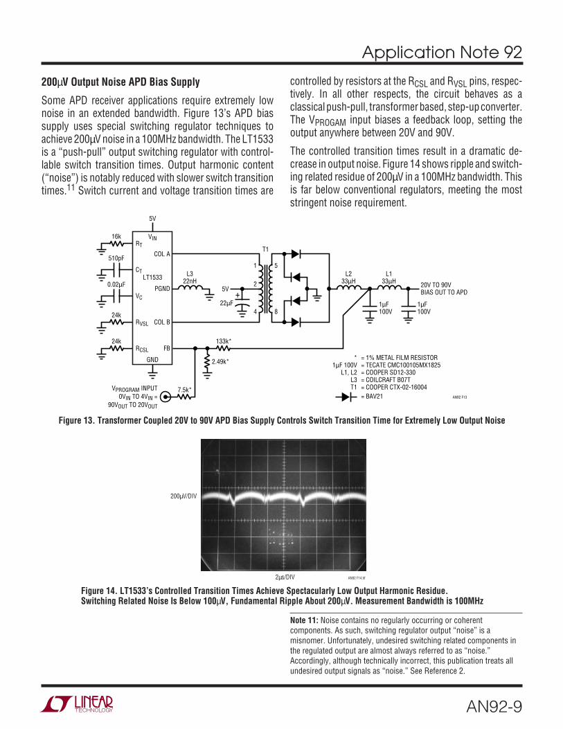
200µV Output Noise APD Bias Supply
Some APD receiver applications require extremely lownoise in an extended bandwidth. Figure 13’s APD biassupply uses special switching regulator techniques toachieve 200µV noise in a 100MHz bandwidth. The LT1533is a “push-pull” output switching regulator with control-lable switch transition times. Output harmonic content(“noise”) is notably reduced with slower switch transitiontimes.11 Switch current and voltage transition times are
controlled by resistors at the RCSL and RVSL pins, respec-tively. In all other respects, the circuit behaves as aclassical push-pull, transformer based, step-up converter.The VPROGAM input biases a feedback loop, setting theoutput anywhere between 20V and 90V.
The controlled transition times result in a dramatic de-crease in output noise. Figure 14 shows ripple and switch-ing related residue of 200µV in a 100MHz bandwidth. Thisis far below conventional regulators, meeting the moststringent noise requirement.
4
1
8
5
25V
22µF
L322nH
T1
+
L233µH
L133µH
16k
24k
24k
510pF
0.02µF
CT
VC
RTVIN
LT1533
5V
GND
RVSL
PGND
COL A
COL B
RCSL FB
2.49k*
AN92 F13
1µF100V
1µF100V
20V TO 90VBIAS OUT TO APD
7.5k*VPROGRAM INPUT0VIN TO 4VIN =
90VOUT TO 20VOUT
133k*
= BAV21
= 1% METAL FILM RESISTOR= TECATE CMC100105MX1825= COOPER SD12-330= COILCRAFT B07T= COOPER CTX-02-16004
*1µF 100V
L1, L2L3T1
2µs/DIV AN92 F14.tif
200µV/DIV
Figure 13. Transformer Coupled 20V to 90V APD Bias Supply Controls Switch Transition Time for Extremely Low Output Noise
Note 11: Noise contains no regularly occurring or coherentcomponents. As such, switching regulator output “noise” is amisnomer. Unfortunately, undesired switching related components inthe regulated output are almost always referred to as “noise.”Accordingly, although technically incorrect, this publication treats allundesired output signals as “noise.” See Reference 2.
Figure 14. LT1533’s Controlled Transition Times Achieve Spectacularly Low Output Harmonic Residue.Switching Related Noise Is Below 100µV, Fundamental Ripple About 200µV. Measurement Bandwidth is 100MHz
Application Note 92
AN92-10
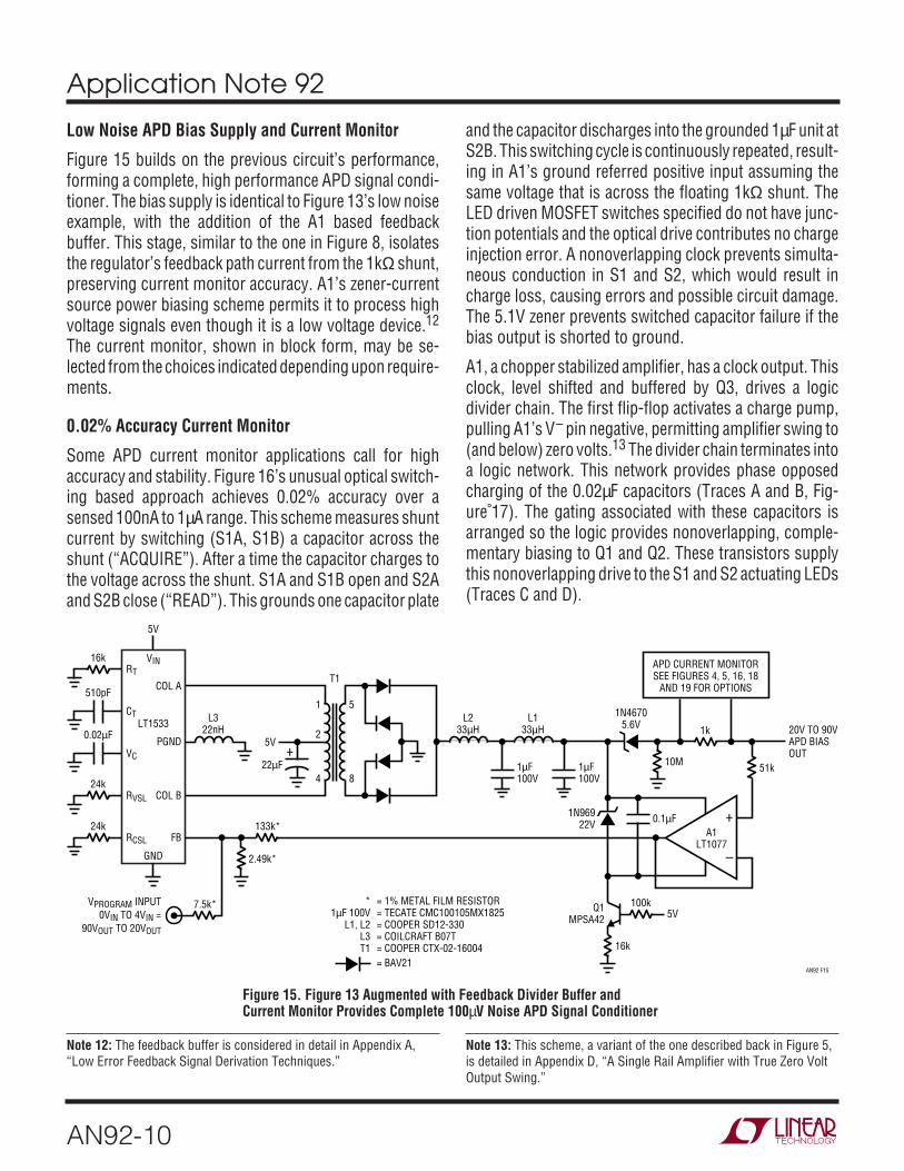
Low Noise APD Bias Supply and Current Monitor
Figure 15 builds on the previous circuit’s performance,forming a complete, high performance APD signal condi-tioner. The bias supply is identical to Figure 13’s low noiseexample, with the addition of the A1 based feedbackbuffer. This stage, similar to the one in Figure 8, isolatesthe regulator’s feedback path current from the 1kΩ shunt,preserving current monitor accuracy. A1’s zener-currentsource power biasing scheme permits it to process highvoltage signals even though it is a low voltage device.12
The current monitor, shown in block form, may be se-lected from the choices indicated depending upon require-ments.
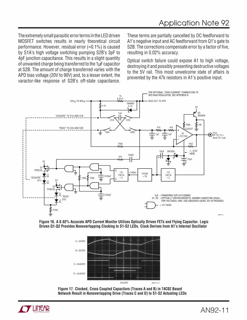
0.02% Accuracy Current Monitor
Some APD current monitor applications call for highaccuracy and stability. Figure 16’s unusual optical switch-ing based approach achieves 0.02% accuracy over asensed 100nA to 1µA range. This scheme measures shuntcurrent by switching (S1A, S1B) a capacitor across theshunt (“ACQUIRE”). After a time the capacitor charges tothe voltage across the shunt. S1A and S1B open and S2Aand S2B close (“READ”). This grounds one capacitor plate
and the capacitor discharges into the grounded 1µF unit atS2B. This switching cycle is continuously repeated, result-ing in A1’s ground referred positive input assuming thesame voltage that is across the floating 1kΩ shunt. TheLED driven MOSFET switches specified do not have junc-tion potentials and the optical drive contributes no chargeinjection error. A nonoverlapping clock prevents simulta-neous conduction in S1 and S2, which would result incharge loss, causing errors and possible circuit damage.The 5.1V zener prevents switched capacitor failure if thebias output is shorted to ground.
A1, a chopper stabilized amplifier, has a clock output. Thisclock, level shifted and buffered by Q3, drives a logicdivider chain. The first flip-flop activates a charge pump,pulling A1’s V– pin negative, permitting amplifier swing to(and below) zero volts.13 The divider chain terminates intoa logic network. This network provides phase opposedcharging of the 0.02µF capacitors (Traces A and B, Fig-ure 17). The gating associated with these capacitors isarranged so the logic provides nonoverlapping, comple-mentary biasing to Q1 and Q2. These transistors supplythis nonoverlapping drive to the S1 and S2 actuating LEDs(Traces C and D).
4
1
8
5
25V
22µF
L322nH
T1
+
L233µH
L133µH
16k
24k
24k
510pF
0.02µF
CT
VC
RTVIN
LT1533
5V
GND
RVSL
PGND
COL A
COL B
RCSL FB
2.49k*
AN92 F15
1µF100V
1µF100V
1N96922V
20V TO 90VAPD BIAS OUT
APD CURRENT MONITORSEE FIGURES 4, 5, 16, 18
AND 19 FOR OPTIONS
7.5k*VPROGRAM INPUT0VIN TO 4VIN =
90VOUT TO 20VOUT
133k*
= BAV21
= 1% METAL FILM RESISTOR= TECATE CMC100105MX1825= COOPER SD12-330= COILCRAFT B07T= COOPER CTX-02-16004
*1µF 100V
L1, L2L3T1
–
+A1
LT1077
51k10M
1k
100k5V
16k
Q1MPSA42
0.1µF
1N46705.6V
Figure 15. Figure 13 Augmented with Feedback Divider Buffer andCurrent Monitor Provides Complete 100µV Noise APD Signal Conditioner
Note 12: The feedback buffer is considered in detail in Appendix A,“Low Error Feedback Signal Derivation Techniques.”
Note 13: This scheme, a variant of the one described back in Figure 5,is detailed in Appendix D, “A Single Rail Amplifier with True Zero VoltOutput Swing.”
Application Note 92
AN92-11
Q1TP0610L
“ACQUIRE”(S1)
“READ”(S2)
“ACQUIRE” TO S1A AND S1B
“READ” TO S2A AND S2B
0.02µF
≈140Hz
10µF
10µF
IOUT0V TO 1V = 0mA TO 1mA
AN92 F16
BAT85s
510Ω
Q2TP0610L
5V
5V130k130k
0.02µF
Q1/2
74C74÷ 2
1/274C74
÷ 2Q
++
≈ –3.5VHERE
–
+
10Ω
A1LTC1150
47k
10k
5V
Q32N3906
100k
CLKOUT
1µF
47k
1µF
1µF
5.1k
BIAS OUT TO APD20VIN TO 90VIN
S1A S1B
S2A S2B
47k
150pF
750k
1k0.01%
1N46895.1V
FOR OPTIONAL “ZERO CURRENT” CONNECTION TOAPD BIAS REGULATOR, SEE APPENDIX A
= PANASONIC ECP-U1C105MA5= OPTICALLY DRIVEN MOSFETS. AROMAT AQW227NA (DUAL) FOR VOLTAGES <80V, USE AQS225SX (QUAD, SO-16 PACKAGE)
= 1/4 74C02
1µFS1, S2
74C90÷ 10
The extremely small parasitic error terms in the LED drivenMOSFET switches results in nearly theoretical circuitperformance. However, residual error (≈0.1%) is causedby S1A’s high voltage switching pumping S2B’s 3pF to4pF junction capacitance. This results in a slight quantityof unwanted charge being transferred to the 1µF capacitorat S2B. The amount of charge transferred varies with theAPD bias voltage (20V to 90V) and, to a lesser extent, thevaractor-like response of S2B’s off-state capacitance.
These terms are partially cancelled by DC feedforward toA1’s negative input and AC feedforward from Q1’s gate toS2B. The corrections compensate error by a factor of five,resulting in 0.02% accuracy.
Optical switch failure could expose A1 to high voltage,destroying it and possibly presenting destructive voltagesto the 5V rail. This most unwelcome state of affairs isprevented by the 47k resistors in A1’s positive input.
Figure 16. A 0.02% Accurate APD Current Monitor Utilizes Optically Driven FETs and Flying Capacitor. LogicDriven Q1-Q2 Provides Nonoverlapping Clocking to S1-S2 LEDs. Clock Derives from A1’s Internal Oscillator
2ms/DIV AN92 F17.tif
A = 5V/DIV
Figure 17. Clocked, Cross Coupled Capacitors (Traces A and B) in 74C02 BasedNetwork Result in Nonoverlapping Drive (Traces C and D) to S1-S2 Actuating LEDs
B = 5V/DIV
C = 5mA/DIV
D = 5mA/DIV

Application Note 92
AN92-12
Digital Output 0.09% Accuracy Current Monitor
Figure 18 modifies the optically based current monitor tosupply a digital output. The schematic is essentially iden-tical to Figure 16’s, with two significant differences. Here,a digital output is supplied via the LTC2431 A-to-D con-verter. The converter’s differential inputs allow the samefeedforward based error correction used in the previousexample. The divider chain countdown ratio has changedto accomodate a higher speed clock, sourced by theLTC1799 oscillator. This higher speed clock, which timesA-to-D operation, centers the A-to-D’s internal notch filterat the optical switches commutation frequency, maximiz-ing rejection.14
This circuit’s 0.09% accuracy does not equal the previousanalog ouput’s version because of the LT1460 reference’s0.075% tolerance, which is not trimmable. The circuit canbe adjusted to 0.02% accuracy by trimming the 1kΩ shuntso measured output current directly corresponds to A-to-Doutput.
Digital Output Current Monitor
Previous current monitor examples furnish digital outputfrom ground referenced A-to-D converters fed from ana-log level shifting stages. Figure 19 directly digitizes shuntcurrent by floating the A-to-D converter in the APD biasline. The A-to-D output is level shifted in the digital
Note 14: The LTC2431’s internal digital filter’s first null occurs at1/2560 of the frequency applied to its FO pin. For details, see theLTC2431 data sheet.
TP0610L
“ACQUIRE”(S1)
“READ”(S2)
“ACQUIRE” TO S1A AND S1B
“READ” TO S2A AND S12B
0.02µF
≈140Hz
AN92 F18
510Ω
TP0610L
5V
5V130k
56.2k*
5V
130k0.02µF
Q1/2
74C74÷ 2
74C90÷ 10
CD4024÷ 128
Q
LTC1799
RSET
OUT
VIN GND
47k
10Ω
1µF
1µF
S1A S1B
S2A S2B
33k
33k
150pF
750k
1k0.01%
= 1% METAL FILM RESISTOR= PANASONIC ECP-U1C105MA5= OPTICALLY DRIVEN MOSFETS. AROMAT AQW227NA (DUAL) FOR VOLTAGES <80V, USE AQS225SX (QUAD, SO-16 PACKAGE)= 1/4 74C02
*1µF
S1, S2
LTC2431A-TO-D
GND
VIN–
VIN+
CS
VREF
V+
5V
FO
5V
SCK DIGITALINTERFACE
≈179kHz
SDO
LT14602.5V
5.1k
BIAS OUT TO APD20VIN TO 90VIN1N4689
5.1V
FOR OPTIONAL “ZERO CURRENT” FEEDBACK CONNECTION TO APD BIAS REGULATOR, SEE APPENDIX A
Figure 18. Figure 16’s Optically Driven FET Based Current Monitor Modified for Digital Output.LTC1799 Clocks A-to-D and Optical Switch LEDs. 0.09% Accuracy, Trimmable to 0.02%

Application Note 92
AN92-13
domain, presenting ground referred digital data. Thissimple approach is attractive, although the available APDbias supply must supply about 3mA to the A-to-D and itsattendant circuitry.
The LTC2410 and its LT1029 reference are powereddirectly from the high voltage APD bias supply input.Current sink Q3 and the LT1029 bias the LTC2410 V– pin,maintaining 5V across the A-to-D over the 20V to 90V biasrail range. The A-to-D’s differential inputs measure acrossthe 1kΩ current shunt. Resistors and a zener clampprotect the A-to-D from excessive voltages if the APD biasline is shorted to ground. The A-to-D’s digital outputs,floating at high voltage, drive level shifts which provide
ground referred data. One of the identical stages is shown;the other indicated in conceptual form. The stage isdesigned for low quiescent and dynamic current con-sumption while maintaining data fidelity. This is necessaryto minimize current drain from the APD bias supply and toavoid modulating it with transient loading artifacts. Highvoltage common emitter Q1 sources current to Q2, whichprovides a ground referred logic compatible output. Ca-pacitive feedforwards maintain data edge speed whileminimizing standing current requirements.
This circuit’s 0.25% untrimmed accuracy is due to shuntand LT1029 tolerances. Trimming the LT1029 (see sche-matic note) permits 0.05% accuracy.
SDOOUT
AN92 F19
1M
LT10295V
1N46895.1V
TRIM(SEENOTES)
10µF
LT1029 TRIM PERMITS HIGHER ACCURACY. SEE DATA SHEET
LTC2410
LEVEL SHIFTIDENTICALTO Q1-Q2
STAGE
SCKOUT
SDO
+
–
V –
CS
VREF–
V+
SCK
VREF
1k0.05%
5.1k
VIN20V TO 90V
5.1k
33k
33k
5pF
Q22N2369
Q12N5400
33k1k
5V
Q3MPSA42
10k
470pF
2.2k
47k5V
BIAS OUT TO APD
FOR OPTIONAL “ZERO CURRENT” FEEDBACK CONNECTION TO APD BIAS REGULATOR, SEE APPENDIX A
Figure 19. A-to-D Converter Floats at High Voltage, Forming Digital Output Current Monitor.Q1-Q2 Level Shift Provides Ground Referenced Digital Output. 0.25% Accuracy Is Trimmable to 0.05%
Application Note 92
AN92-14
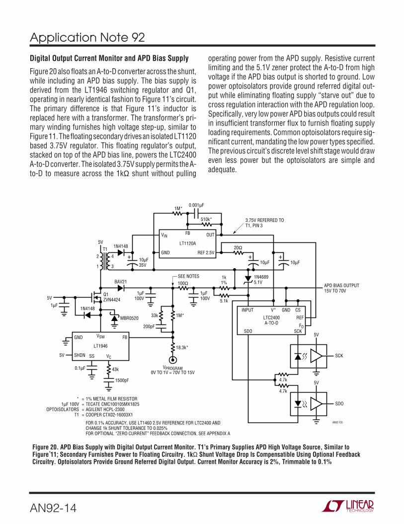
Digital Output Current Monitor and APD Bias Supply
Figure 20 also floats an A-to-D converter across the shunt,while including an APD bias supply. The bias supply isderived from the LT1946 switching regulator and Q1,operating in nearly identical fashion to Figure 11’s circuit.The primary difference is that Figure 11’s inductor isreplaced here with a transformer. The transformer’s pri-mary winding furnishes high voltage step-up, similar toFigure 11. The floating secondary drives an isolated LT1120based 3.75V regulator. This floating regulator’s output,stacked on top of the APD bias line, powers the LTC2400A-to-D converter. The isolated 3.75V supply permits the A-to-D to measure across the 1kΩ shunt without pulling
operating power from the APD supply. Resistive currentlimiting and the 5.1V zener protect the A-to-D from highvoltage if the APD bias output is shorted to ground. Lowpower optoisolators provide ground referred digital out-put while eliminating floating supply “starve out” due tocross regulation interaction with the APD regulation loop.Specifically, very low power APD bias outputs could resultin insufficient transformer flux to furnish floating supplyloading requirements. Common optoisolators require sig-nificant current, mandating the low power types specified.The previous circuit’s discrete level shift stage would draweven less power but the optoisolators are simple andadequate.
31
42
LT1120A
FBVIN
1µF100V
100ΩSEE NOTES
APD BIAS OUTPUT15V TO 70V
1M*
1µF100V
200pF
1k1%
5.1k
18.3k*
SCK
5V
VPROGRAM0V TO 1V = 70V TO 15V
33k
AN92 F20
BAV21
1µF
0.1µF
1500pF
10µF35V
GND
OUT
REF 2.5V+
1N41485V
T1
1N4148
Q1ZVN4424
MBR0520
LT1946
VSW
SS VC
GND
SHDN5V
5V
FB
LTC2400A-TO-D
V+
REF
FO
GND CSINPUT
SCKSDO
510k*
1M*0.001µF
10µF
3.75V REFERRED TOT1, PIN 3
1N46895.1V
20Ω
10µF+
43k
SDO
5V4.7k
4.7k
= 1% METAL FILM RESISTOR= TECATE CMC100105MX1825= AGILENT HCPL-2300= COOPER CTX02-16003X1
FOR 0.1% ACCURACY, USE LT1460 2.5V REFERENCE FOR LTC2400 ANDCHANGE 1k SHUNT TOLERANCE TO 0.025%FOR OPTIONAL “ZERO CURRENT” FEEDBACK CONNECTION, SEE APPENDIX A
*1µF 100V
OPTOISOLATORST1
+
Figure 20. APD Bias Supply with Digital Output Current Monitor. T1’s Primary Supplies APD High Voltage Source, Similar toFigure 11; Secondary Furnishes Power to Floating Circuitry. 1kΩ Shunt Voltage Drop Is Compensatible Using Optional FeedbackCircuitry. Optoisolators Provide Ground Referred Digital Output. Current Monitor Accuracy is 2%, Trimmable to 0.1%

Application Note 92
AN92-15
Note: This application note was derived from a manuscript originallyprepared for publication in EDN magazine.
The LT1120 2.5V reference and 1kΩ shunt tolerancesdictate 2% circuit accuracy. If the tighter tolerance com-ponents noted in the schematic are used, 0.1% accuracyis practical.
ANALOG DIGITALOUTPUT OUTPUT
BIAS CURRENT CURRENTFIGURE SUPPLY MONITOR MONITORNUMBER CAPABILITY (100nA to 1mA) (100nA to 1mA) COMMENTS
4 No Yes No 0.4% Accuracy. High Noise Rejection
5 No Yes Yes 0.5% Accuracy. Draws Current from APD Bias Supply Approximately Equalling CurrentDelivered to the APD in Addition to Housekeeping Current
6 Yes No No 200µV Noise in 10MHz Bandwidth. 3% Accuracy30V to 90V
8 Yes Yes No 3% Bias Voltage Accuracy. 0.5% Current Monitor Accuracy.30V to 85V Current Monitor Has 1kΩ Output Impedance
9 Yes Yes No 0.25% Bias Voltage Accuracy. 1mV Output Noise in 10MHz Bandwidth.20V to 90V 0.25% Current Monitor Accuracy. Small Size. Few Large Value, High Voltage
Capacitors Improves Reliability. Low Current Drain from APD Rail Permits SmallerHigh Voltage Capacitors for a Given Ripple Level
11 Yes No No 2% Bias Voltage Accuracy. 1.5mV Output Noise in 10MHz Bandwidth.20V to 90V Small Size, Simple
13 Yes No No 2% Bias Voltage Accuracy. 200µV Ripple and Noise in 100MHz Bandwidth.20V to 90V Relatively Large Solution Size Due to 250kHz Oscillator Frequency
15 Yes Yes Yes 2% Bias Voltage Accuracy. 200µV Ripple and Noise in 100MHz Bandwidth.20V to 90V Current Monitor Accuracy Depends on Option Selected. Relatively Large Solution Size
Due to 250kHz Oscillator Frequency
16 No Yes No 0.02% Accuracy. Low Current Drain from APD Rail Permits Smaller High VoltageCapacitors for a Given Ripple Level
18 No No Yes 0.09% Accuracy. 0.02% Achievable with Shunt Trimming. Low Current Drain fromAPD Rail Permits Smaller High Voltage Capacitors for a Given Ripple Level
19 No No Yes 0.25% Accuracy. Trimmable to 0.05% by Adjusting Reference
20 Yes No Yes 2% Bias Voltage Accuracy. 2% Current Monitor Accuracy.15V to 70V 0.1% Accuracy Obtainable with Optional LT1460 Reference. Low Current Drain from
APD Rail Permits Smaller High Voltage Capacitors for a Given Ripple Level
Figure 21. Summarized Characteristics of Techniques Presented. Applicable Circuit Depends on Application Specifics
Summary
Figure 21’s chart is an attempt to summarize the circuitspresented, although such brevity breeds oversimplifica-tion. As such, although the chart reviews salient features,there is no substitute for a thorough investigation of anyparticular application’s requirements.
Application Note 92
AN92-16
APPENDIX A
LOW ERROR FEEDBACK SIGNAL DERIVATIONTECHNIQUES
Various text circuits either detail or make reference tocounteracting loading effects of the APD bias supply’soutput feedback divider. If the divider is located before the1kΩ current shunt, its current drain is not included in thecurrent monitor’s output and no error is incurred. Apotential difficulty with this approach is that the 1kΩ shuntappears in series with the bias supply output, degradingload regulation. The maximum 1mA shunt current pro-duces a 1V output regulation drop. In some cases this ispermissible and no further consideration is required.Circumstances dictating tighter load regulation requirecompensation techniques.
Divider Current Error Compensation—“Low Side”Shunt Case
When the shunt is in a transformer’s return path (“low sideshunt”), divider error is cancelled by introducing a com-pensatory term into the APD current monitor circuitry.
Figure A1 shows details. The output voltage divider’scurrent loading error is prevented from appearing in A1’soutput by feeding forward a compensatory current fromthe APD bias programming input. This compensatingcurrent, arriving at A1 via RLARGE, is scaled to preciselybalance out the portion of shunt output contributed by thevoltage divider’s loading error.
Divider Current Error Compensation—“High Side”Shunt Case
Figure A2 addresses situations where the shunt resides inthe “high side.” Such arrangements involve high commonmode voltages, seemingly mandating a high voltage bufferamplifier to isolate the divider’s current loading. Figure A2shows a way around this, using standard low voltageamplifiers to process high voltage signals. A1, sensingafter the 1kΩ shunt, isolates the feedback divider’s load-ing while permitting the APD bias regulator to include theshunt within its feedback loop. A1 is powered directly fromthe bias regulator’s high voltage output but its V– pin is
REFERENCES
1. Meade, M.L., “Lock-In Amplifiers and Applications,”London, P. Peregrinus, Ltd.
2. Williams, J., “A Monolithic Switching Regulator with100µV Output Noise,” Linear Technology Corpora-tion, Application Note 70, October 1997.
3. Williams, J., “Measurement and Control Circuit Col-lection,” “∆VBE Based Thermometer,” Linear Technol-ogy Corporation, Application Note 45, June 1991,pp. 7–8
4. Williams, J., “Applications for a Switched CapacitorInstrumentation Building Block,” Linear TechnologyCorporation, Application Note 3, July 1985.
5. Williams, J., “Monolithic CMOS-Switch IC Suits Di-verse Applications,” EDN Magazine, October 4, 1984.
6. Williams, J., “A Fourth Generation of LCD BacklightTechnology,” “Floating Lamp Circuits,” Linear Tech-nology Corporation, Application Note 65, November1995, pp. 40–43, Figure 48.
7. Negrete, M., “Fiberoptic Communication SystemsBenefit from Tiny, Low Noise Avalanche PhotodiodeBias Supply,” Linear Technology Corporation, DesignNote 273, December 2001.
8. Martin, A., “Charge Pump Based APD Circuits,” Pri-vate Communication, May 2002.
9. Williams, J., “Applications of New Precision Op Amps,”“Instrumentation Amplifier with VCM = 300V and 160dBCMRR,” Linear Technology Corporation, ApplicationNote 6, January 1985, pp. 1–2.
10. Williams, J., “Bridge Circuits,” “Optically CoupledSwitched Capacitor Instrumentation Amplifier,” Lin-ear Technology Corporation, Application Note 43,June 1990, pp. 9–10
11. Hickman, R. W. and Hunt, F. V., “On Electronic VoltageStabilizers,” “Cascode,” Review of Scientific Instru-ments, January 1939, pp. 6–21, p. 16.

Application Note 92
AN92-17
+
–A1
101k100k
APD CURRENTMONITOR OUTPUT(IAPD – DIVIDER ERROR)
AN92 FA01
TO APD
I = APD + DIVIDER ERROR
10M DIVIDER ERROR CURRENT
THIS POINTGOES NEGATIVE WITHINCREASING CURRENT
(E.G., AT EAPD = 90VDIVIDER ERROR CURRENT = 8.75µA)
287k
OUTPUTVOLTAGEDIVIDER
V+
PWMCONTROLLER
FB
APD BIASPROGRAMMING
INPUT
CURRENTSHUNT
1k
RLARGE
I =EAPD
RDIVIDER
IAPD
FEEDFORWARDCOMPENSATION CURRENT
RLARGE SCALED SOVPROGRAM INDUCED CURRENT =
DIVIDER ERROR CURRENT
Figure A1. Output Voltage Divider Current Loading Error Is Compensated with Feedforward from Programming Input.A1 Algebraically Sums Feedforward Term and Current Shunt Information, Presents Corrected Output
zener clamped with respect to its V+ pin. Current sink Q1maintains this bias over the wide range of possible APDregulator outputs. Although A1 processes high voltagesignals, the voltage across it is held to safe levels. The 5.6Vzener in the APD bias line ensures A1’s inputs are alwaysinside their common mode operating range. The 10M
–
+A1
LT1077
0.1µF1N96922V
1N46905.6V 1k
TO APD BIASREGULATOR
FEEDBACKINPUT
FEEDBACKDIVIDER
Q1MPSA42
100k
16k
5V
AN92 FA02
V+51k
V–
FROM APD BIASREGULATOR
25VIN TO 95VIN
VOUT TO APD
10M
APDCURRENTMONITOR
Figure A2. A1 Follower Floats from High Voltage Rail,Eliminates Feedback Divider Current Loading Error. Q1Current Source and 22V Zener Maintain Low Voltage AcrossAmplifier; 5.6V Zener Accomodates A1’s Input Range
resistor maintains adequate zener bias when APD currentsare extremely low. A 51k resistor protects A1 from de-structive high voltage if the APD bias output is shorted toground. Similarly, the 100k resistor prevents high voltagefrom appearing on the 5V supply if Q1 fails.

Application Note 92
AN92-18
APPENDIX B
PREAMPLIFIER AND OSCILLOSCOPE SELECTION
The low level measurements described require some formof preamplification for the oscilloscope. Current genera-tion oscilloscopes rarely have greater than 2mV/DIV sen-sitivity, although older instruments offer more capability.Figure B1 lists representative preamplifiers and oscillo-scope plug-ins suitable for noise measurement. Theseunits feature wideband, low noise performance. It isparticularly significant that many of these instruments areno longer produced. This is in keeping with current instru-mentation trends, which emphasize digital signal acquisi-tion as opposed to analog measurement capability.
The monitoring oscilloscope should have adequate band-width and exceptional trace clarity. In the latter regard highquality analog oscilloscopes are unmatched. The excep-tionally small spot size of these instruments is well-suitedto low level noise measurement.1 The digitizing uncertain-ties and raster scan limitations of DSOs impose displayresolution penalties. Many DSO displays will not evenregister the small levels of switching-based noise.
INSTRUMENT MODEL MAXIMUMTYPE MANUFACTURER NUMBER BANDWIDTH SENSITIVITY/GAIN AVAILABILITY COMMENTS
Amplifier Hewlett-Packard 461A 150MHz Gain = 100 Secondary Market 50Ω Input, Standalone
Differential Amplifier Tektronix 1A5 50MHz 1mV/DIV Secondary Market Requires 500 Series Mainframe
Differential Amplifier Tektronix 7A13 100MHz 1mV/DIV Secondary Market Requires 7000 Series Mainframe
Differential Amplifier Tektronix 11A33 150MHz 1mV/DIV Secondary Market Requires 11000 Series Mainframe
Differential Amplifier Tektronix P6046 100MHz 1mV/DIV Secondary Market Standalone
Differential Amplifier Preamble 1855 100MHz Gain = 10 Current Production Standalone, Settable Bandstops
Differential Amplifier Preamble 1822 10MHz Gain = 1000 Current Production Standalone, Settable Bandstops
Figure B1. Some Applicable High Sensitivity, Low Noise Amplifiers. Trade-Offs Include Bandwidth, Sensitivity and Availability
Note 1: In our work we have found Tektronix types 453, 453A, 454,454A, 547 and 556 excellent choices. Their pristine trace presentationis ideal for discerning small signals of interest against a noise floorlimited background.
Application Note 92
AN92-19
APPENDIX C
PROBING AND CONNECTION TECHNIQUES FORLOW LEVEL, WIDEBAND SIGNAL INTEGRITY1
The most carefully prepared breadboard cannot fulfill itsmission if signal connections introduce distortion. Con-nections to the circuit are crucial for accurate informationextraction. The low level, wideband measurementsdemand care in routing signals to test instrumentation.
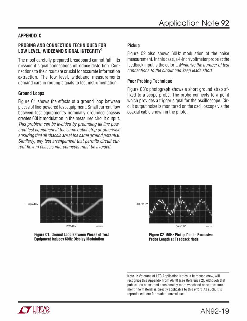
Ground Loops
Figure C1 shows the effects of a ground loop betweenpieces of line-powered test equipment. Small current flowbetween test equipment’s nominally grounded chassiscreates 60Hz modulation in the measured circuit output.This problem can be avoided by grounding all line pow-ered test equipment at the same outlet strip or otherwiseensuring that all chassis are at the same ground potential.Similarly, any test arrangement that permits circuit cur-rent flow in chassis interconnects must be avoided.
Pickup
Figure C2 also shows 60Hz modulation of the noisemeasurement. In this case, a 4-inch voltmeter probe at thefeedback input is the culprit. Minimize the number of testconnections to the circuit and keep leads short.
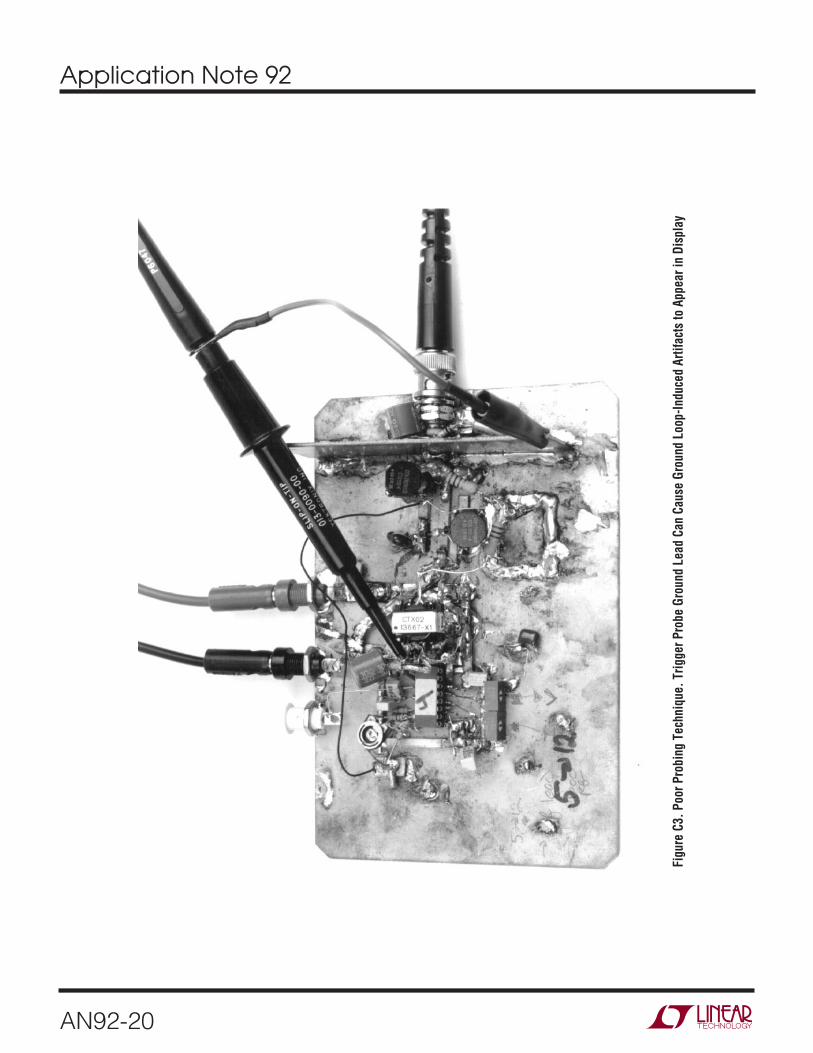
Poor Probing Technique
Figure C3’s photograph shows a short ground strap af-fixed to a scope probe. The probe connects to a pointwhich provides a trigger signal for the oscilloscope. Cir-cuit output noise is monitored on the oscilloscope via thecoaxial cable shown in the photo.
Note 1: Veterans of LTC Application Notes, a hardened crew, willrecognize this Appendix from AN70 (see Reference 2). Although thatpublication concerned considerably more wideband noise measure-ment, the material is directly applicable to this effort. As such, it isreproduced here for reader convenience.
100µV/DIV
2ms/DIV AN92 C01
Figure C1. Ground Loop Between Pieces of TestEquipment Induces 60Hz Display Modulation
500µV/DIV
5ms/DIV AN92 C02
Figure C2. 60Hz Pickup Due to ExcessiveProbe Length at Feedback Node
Application Note 92
AN92-20
Figu
re C
3. P
oor P
robi
ng T
echn
ique
. Trig
ger P
robe
Gro
und
Lead
Can
Cau
se G
roun
d Lo
op-In
duce
d Ar
tifac
ts to
App
ear i
n Di
spla
y
Application Note 92
AN92-21
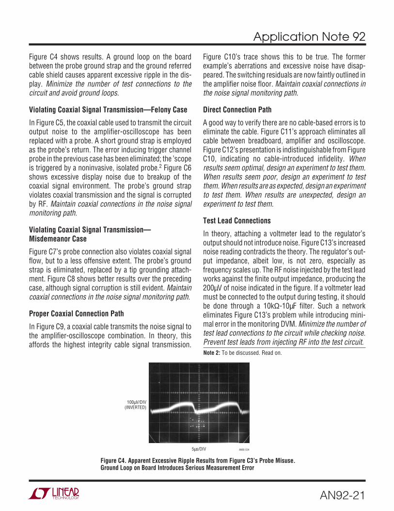
Figure C4 shows results. A ground loop on the boardbetween the probe ground strap and the ground referredcable shield causes apparent excessive ripple in the dis-play. Minimize the number of test connections to thecircuit and avoid ground loops.
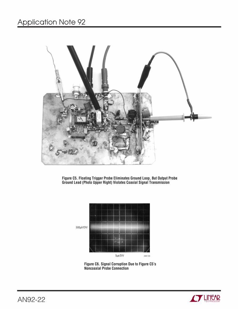
Violating Coaxial Signal Transmission—Felony Case
In Figure C5, the coaxial cable used to transmit the circuitoutput noise to the amplifier-oscilloscope has beenreplaced with a probe. A short ground strap is employedas the probe’s return. The error inducing trigger channelprobe in the previous case has been eliminated; the ’scopeis triggered by a noninvasive, isolated probe.2 Figure C6shows excessive display noise due to breakup of thecoaxial signal environment. The probe’s ground strapviolates coaxial transmission and the signal is corruptedby RF. Maintain coaxial connections in the noise signalmonitoring path.
Violating Coaxial Signal Transmission—Misdemeanor Case
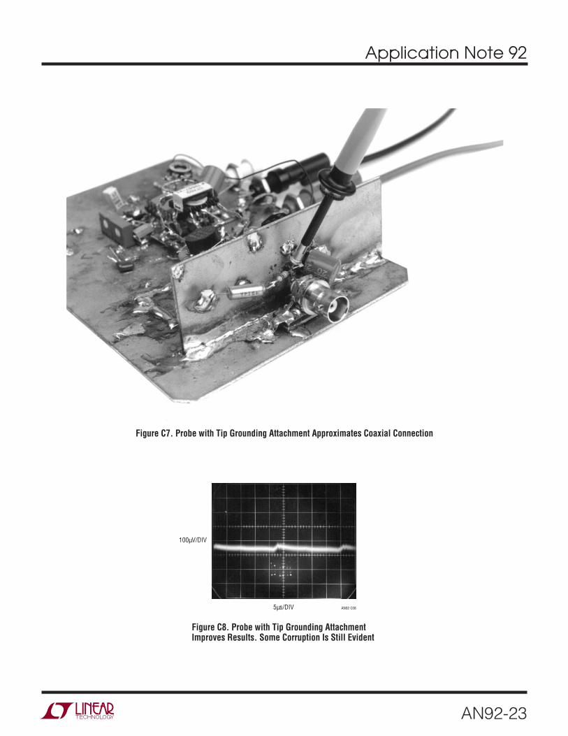
Figure C7’s probe connection also violates coaxial signalflow, but to a less offensive extent. The probe’s groundstrap is eliminated, replaced by a tip grounding attach-ment. Figure C8 shows better results over the precedingcase, although signal corruption is still evident. Maintaincoaxial connections in the noise signal monitoring path.
Proper Coaxial Connection Path
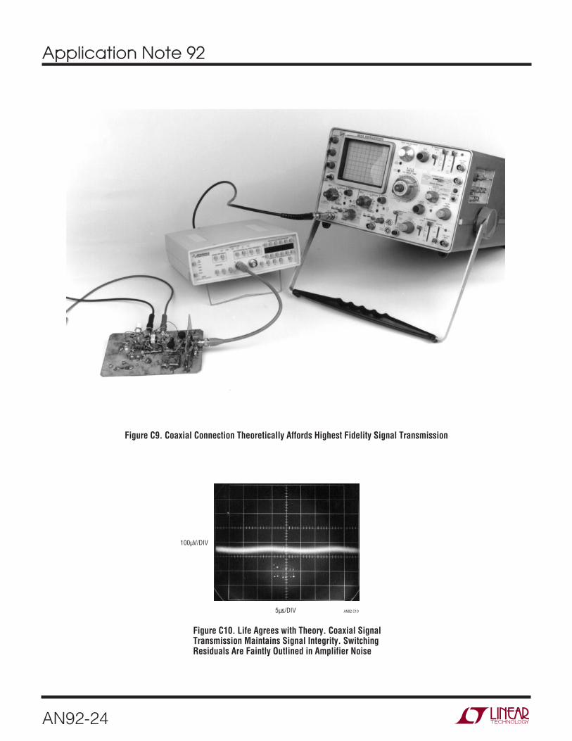
In Figure C9, a coaxial cable transmits the noise signal tothe amplifier-oscilloscope combination. In theory, thisaffords the highest integrity cable signal transmission.
Note 2: To be discussed. Read on.
100µV/DIV(INVERTED)
5µs/DIV AN85 C04
Figure C4. Apparent Excessive Ripple Results from Figure C3’s Probe Misuse.Ground Loop on Board Introduces Serious Measurement Error
Figure C10’s trace shows this to be true. The formerexample’s aberrations and excessive noise have disap-peared. The switching residuals are now faintly outlined inthe amplifier noise floor. Maintain coaxial connections inthe noise signal monitoring path.
Direct Connection Path
A good way to verify there are no cable-based errors is toeliminate the cable. Figure C11’s approach eliminates allcable between breadboard, amplifier and oscilloscope.Figure C12’s presentation is indistinguishable from FigureC10, indicating no cable-introduced infidelity. Whenresults seem optimal, design an experiment to test them.When results seem poor, design an experiment to testthem. When results are as expected, design an experimentto test them. When results are unexpected, design anexperiment to test them.
Test Lead Connections
In theory, attaching a voltmeter lead to the regulator’soutput should not introduce noise. Figure C13’s increasednoise reading contradicts the theory. The regulator’s out-put impedance, albeit low, is not zero, especially asfrequency scales up. The RF noise injected by the test leadworks against the finite output impedance, producing the200µV of noise indicated in the figure. If a voltmeter leadmust be connected to the output during testing, it shouldbe done through a 10kΩ-10µF filter. Such a networkeliminates Figure C13’s problem while introducing mini-mal error in the monitoring DVM. Minimize the number oftest lead connections to the circuit while checking noise.Prevent test leads from injecting RF into the test circuit.
Application Note 92
AN92-22
500µV/DIV
5µs/DIV AN92 C06
Figure C6. Signal Corruption Due to Figure C5’sNoncoaxial Probe Connection
Figure C5. Floating Trigger Probe Eliminates Ground Loop, But Output ProbeGround Lead (Photo Upper Right) Violates Coaxial Signal Transmission
Application Note 92
AN92-23
Figure C7. Probe with Tip Grounding Attachment Approximates Coaxial Connection
100µV/DIV
5µs/DIV AN92 C08
Figure C8. Probe with Tip Grounding AttachmentImproves Results. Some Corruption Is Still Evident
Application Note 92
AN92-24
Figure C9. Coaxial Connection Theoretically Affords Highest Fidelity Signal Transmission
100µV/DIV
5µs/DIV AN92 C10
Figure C10. Life Agrees with Theory. Coaxial SignalTransmission Maintains Signal Integrity. SwitchingResiduals Are Faintly Outlined in Amplifier Noise

Application Note 92
AN92-25
Figure C11. Direct Connection to Equipment Eliminates Possible Cable-TerminationParasitics, Providing Best Possible Signal Transmission
100µV/DIV
5µs/DIV AN92 C12
Figure C12. Direct Connection to Equipment ProvidesIdentical Results to Cable-Termination Approach.Cable and Termination Are Therefore Acceptable

Application Note 92
AN92-26
200µV/DIV
5µs/DIV AN92 C13
Figure C13. Voltmeter Lead Attached to Regulator OutputIntroduces RF Pickup, Multiplying Apparent Noise Floor
1k
4700pF
L1: J.W. MILLER #100267AN92 FC14
TERMINATION BOXSHIELDED
CABLE
L1PROBE
BNC CONNECTIONTO TERMINATION BOX
DAMPINGADJUST
BNCOUTPUT
Figure C14. Simple Trigger Probe Eliminates BoardLevel Ground Loops. Termination Box ComponentsDamp L1’s Ringing Response
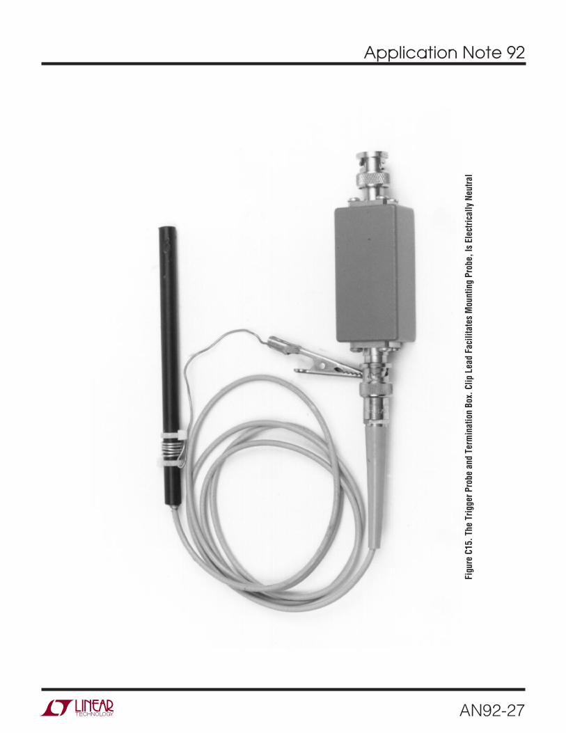
Isolated Trigger Probe
The text associated with Figure C5 somewhat crypticallyalluded to an “isolated trigger probe.” Figure C14 revealsthis to be simply an RF choke terminated against ringing.The choke picks up residual radiated field, generating anisolated trigger signal. This arrangement furnishes a ’scopetrigger signal with essentially no measurement corrup-tion. The probe’s physical form appears in Figure C15. Forgood results, the termination should be adjusted forminimum ringing while preserving the highest possibleamplitude output. Light compensatory damping producesFigure C16’s output, which will cause poor ’scope trigger-ing. Proper adjustment results in a more favorable output(Figure C17), characterized by minimal ringing and well-defined edges.
Trigger Probe Amplifier
The field around the switching magnetics is small and maynot be adequate to reliably trigger some oscilloscopes. Insuch cases, Figure C18’s trigger probe amplifier is useful.It uses an adaptive triggering scheme to compensate forvariations in probe output amplitude. A stable 5V triggeroutput is maintained over a 50:1 probe output range. A1,operating at a gain of 100, provides wideband AC gain. Theoutput of this stage biases a 2-way peak detector (Q1through Q4). The maximum peak is stored in Q2’s emittercapacitor, while the minimum excursion is retained in Q4’s
emitter capacitor. The DC value of the midpoint of A1’soutput signal appears at the junction of the 500pF capaci-tor and the 3MΩ units. This point always sits midwaybetween the signal’s excursions, regardless of absoluteamplitude. This signal-adaptive voltage is buffered by A2to set the trigger voltage at the LT1394’s positive input.The LT1394’s negative input is biased directly from A1’soutput. The LT1394’s output, the circuit’s trigger output,is unaffected by >50:1 signal amplitude variations. AnX100 analog output is available at A1.
Figure C19 shows the circuit’s digital output (Trace B)responding to the amplified probe signal at A1 (Trace A).
Figure C20 is a typical noise testing setup. It includes thebreadboard, trigger probe, amplifier, oscilloscope andcoaxial components.
Application Note 92
AN92-27
Figu
re C
15. T
he T
rigge
r Pro
be a
nd T
erm
inat
ion
Box.
Clip
Lea
d Fa
cilit
ates
Mou
ntin
g Pr
obe,
Is E
lect
rical
ly N
eutra
l

Application Note 92
AN92-28
10mV/DIV
10µs/DIV AN92 C16
Figure C16. Misadjusted Termination Causes InadequateDamping. Unstable Oscilloscope Triggering May Result
10mV/DIV
10µs/DIV AN92 C17
Figure C17. Properly Adjusted TerminationMinimizes Ringing with Small Amplitude Penalty
ANALOG BNC OUTPUTTO ’SCOPE TRIGGER INPUT
DIGITALTRIGGEROUT BNCTO ’SCOPE
5V
–
+A1
LT1227
–
+A2
LT1006
5V
5V
5V
AN92 C18
500pF
0.1µF
1k
470Ω
470Ω
750Ω
10Ω
13
2 4
1413
15
56
1210
11
2k
TRIGGER PROBEAND TERMINATION BOX
(SEE FIGURE C14 FOR DETAILS)
10µF
2k
2k+0.1µF
0.1µF
0.005µF
0.005µF
100µF+
Q1, Q2, Q3, Q4 = CA3096 ARRAY: TIE SUBSTRATE (PIN 16) TO GROUND= 1N4148
–
+
LT1394
Q1 Q2
Q3 Q4
3M
50Ω
3M
Figure C18. Trigger Probe Amplifier Has Analog and Digital Outputs. AdaptiveThreshold Maintains Digital Output Over 50:1 Probe Signal Variations
A = 1V/DIVAC COUPLED
B = 5V/DIV
10µs/DIV (UNCALIB) AN92 C19
Figure C19. Trigger Probe Amplifier Analog (Trace A)and Digital (Trace B) Outputs

Application Note 92
AN92-29
Figu
re C
20. T
ypic
al N
oise
Tes
t Set
up In
clud
es T
rigge
r Pro
be, A
mpl
ifier
, Osc
illos
cope
and
Coa
xial
Com
pone
nts
Application Note 92
AN92-30
–
+
Q12N3904
10µF
10µF
39k
100k
AN92 FD01
1k
5V
1k
≈ –3.5VHERE
V –
V +
5V
A1LTC1150
CLKOUT
100Ω
+
+
DASHED LINE CIRCUITRY = CLAMP OPTIONS. SEE TEXT
= BAT85
APPENDIX D
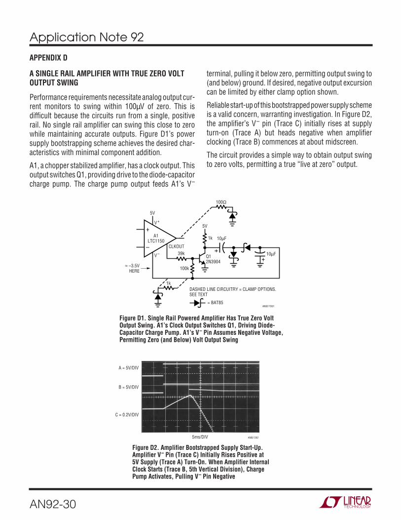
A SINGLE RAIL AMPLIFIER WITH TRUE ZERO VOLTOUTPUT SWING
Performance requirements necessitate analog output cur-rent monitors to swing within 100µV of zero. This isdifficult because the circuits run from a single, positiverail. No single rail amplifier can swing this close to zerowhile maintaining accurate outputs. Figure D1’s powersupply bootstrapping scheme achieves the desired char-acteristics with minimal component addition.
A1, a chopper stabilized amplifier, has a clock output. Thisoutput switches Q1, providing drive to the diode-capacitorcharge pump. The charge pump output feeds A1’s V–
terminal, pulling it below zero, permitting output swing to(and below) ground. If desired, negative output excursioncan be limited by either clamp option shown.
Reliable start-up of this bootstrapped power supply schemeis a valid concern, warranting investigation. In Figure D2,the amplifier’s V– pin (Trace C) initially rises at supplyturn-on (Trace A) but heads negative when amplifierclocking (Trace B) commences at about midscreen.
The circuit provides a simple way to obtain output swingto zero volts, permitting a true “live at zero” output.
Figure D1. Single Rail Powered Amplifier Has True Zero VoltOutput Swing. A1’s Clock Output Switches Q1, Driving Diode-Capacitor Charge Pump. A1’s V– Pin Assumes Negative Voltage,Permitting Zero (and Below) Volt Output Swing
A = 5V/DIV
5ms/DIV AN92 D02
Figure D2. Amplifier Bootstrapped Supply Start-Up.Amplifier V– Pin (Trace C) Initially Rises Positive at5V Supply (Trace A) Turn-On. When Amplifier InternalClock Starts (Trace B, 5th Vertical Division), ChargePump Activates, Pulling V– Pin Negative
B = 5V/DIV
C = 0.2V/DIV

Application Note 92
AN92-31
APPENDIX E
APD PROTECTION CIRCUITS
APD receiver modules are electrically delicate and expen-sive devices. Because of this, Figure E1’s protection cir-cuits may be of interest. They are designed to protect theAPD module from bias programming overvoltage error(Figure E1a), excessive current (E1b) or destructive volt-age (Figure E1c). In Figure E1a, Q1 is normally off andprogramming voltage passes to the bias regulator voltageprogramming input. Abnormally high inputs, defined bythe potentiometer’s setting, cause A1 to swing low, bias-ing Q1 and closing A1’s feedback loop. This causes Q1’semitter to clamp at the potentiometer wiper’s voltage,safely limiting the bias regulator’s programming input.
Figure E1b is an APD current limiter. This particular circuitis designed for use with “low side” shunts in transformercoupled APD supplies, such as text Figure 9, although thetechnique is generally applicable. As long as the shunt
current’s absolute value is below the current limit point, A2is saturated high and the associated APD bias regulatorfunctions normally. Shunt overcurrent forces A2’s outputlower, pulling the regulator’s control pin (VC) lower andlimiting current. The 100pF-1MΩ combination stabilizesA2 and the bias regulator assumes the characteristics of acurrent source.
Figure E1c is an overvoltage crowbar. It is intended as thelast line of defense against uncontrolled APD bias supplyhigh voltage outputs. Normally, the LTC1696 crowbar ICis below its 0.88V trigger threshold and the SCR is off. Ifthe APD bias rises too high the LTC1696 triggers, firing theSCR. SCR turn-on “crowbars” the APD bias line, arrestingthe high voltage and maintaining a short across the line viaits latch characteristic. If the APD bias supply has signifi-cant output impedance, prolonged SCR loading is notdeleterious; if not, the bias supply should be fused.
+
–A1
LT1006
VOLTAGECLAMPADJUST
4.7k
50k
5V
100Ω Q12N3906
TO BIAS REGULATORVOLTAGE PROGRAMMINGINPUT
INPUT FROMPROGRAMMING VOLTAGE
1K
–
+A2
LT1077
1M
1M*
1M* 100pF
TO APD BIASREGULATOR VC PIN
TO UNGROUNDEDSIDE OF 1kΩ SHUNT
AT TRANSFORMER
CURRENT LIMIT INPUT0V TO 1V = 0mA TO 1mA
SHUNT DERIVEDCURRENT
LIMITCURRENT
TO APD BIASOUTPUT
OUTFB1 LTC1696
+V
5V
GND
R
0.001µF
2N5063
VTRIG = 75.3V AN92 FE01c
AN92 FE01b
AN92 FE01a
88.7k*
7.5M*
TRIG AT0.88V
= 1N4148= 1% METAL FILM RESISTOR*
Figure E1. Protection Circuits Prevent APD Destruction Due to Hardware or Software Failures. Options IncludeProgramming Voltage Clamp (Figure E1a), Current Limiter (Figure E1b) and Bias Voltage Crowbar (Figure E1c)
(E1a) Programming Voltage Clamp
(E1b) Current Limiter (E1c) Bias Voltage Crowbar
Information furnished by Linear Technology Corporation is believed to be accurate and reliable.However, no responsibility is assumed for its use. Linear Technology Corporation makes no represen-tation that the interconnection of its circuits as described herein will not infringe on existing patent rights.
Application Note 92
AN92-32an92f LT/TP 1102 2K • PRINTED IN USA
LINEAR TECHNOLOGY CORPORATION 2002
Linear Technology Corporation1630 McCarthy Blvd., Milpitas, CA 95035-7417(408) 432-1900 FAX: (408) 434-0507 www.linear.com


![Chapter 5 BJT Biasing Circuits Engineering/833... · 2017. 12. 8. · BJT Biasing Circuits 5.1 The DC Operation Point [5] DC Bias: Bias establishes the dc operating point for proper](https://img.pdfslide.us/doc/110x75/6109b3612d57d967952ea81a/chapter-5-bjt-biasing-circuits-engineering833-2017-12-8-bjt-biasing-circuits.jpg)