Embed Size (px)
Citation preview
MVJCE III SEMESTER COURSE DIARY
Telecommunication Engineering PAGE 1
10ES32 – ANALOG ELECTRONIC CIRCUITS
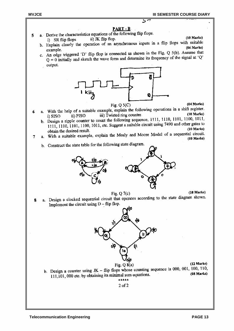
MVJCE III SEMESTER COURSE DIARY
Telecommunication Engineering PAGE 2
SYLLABUS
Sub Code: 10ES32 I A Marks: 25 Hours / Week: 05 Exam Hours: 03 Total Hours: 62 Exam Marks: 100
UNIT 1: Diode Circuits: Diode Resistance, Diode equivalent circuits, Transition and diffusion capacitance, Reverse recovery time, Load line analysis, Rectifiers, Clippers and clampers. UNIT 2: Transistor Biasing: Operating point, Fixed bias circuits, Emitter stabilized biased circuits, Voltage divider biased, DC bias with voltage feedback, Miscellaneous bias configurations, Design operations, Transistor switching networks, PNP transistors, Bias stabilization. UNIT 3: Transistor at Low Frequencies: BJT transistor modeling, CE Fixed bias configuration, Voltage divider bias, Emitter follower, CB configuration, Collector feedback configuration, Analysis of circuits re model; analysis of CE configuration using h- parameter model; Relationship between h-parameter model of CE,CC and CB configuration. UNIT 4: Transistor Frequency Response: General frequency considerations, low frequency response, Miller effect capacitance, High frequency response, multistage frequency effects. UNIT 5: (a) General Amplifiers: Cascade connections, Cascode connections, Darlington connections. (b) Feedback Amplifier: Feedback concept, Feedback connections type,Practical feedback circuits. Design procedures for the feedback amplifiers. UNIT 6: Power Amplifiers: Definitions and amplifier types, series fed class A amplifier, Transformer coupled Class A amplifiers, Class B amplifier operations, Class B amplifier circuits, Amplifier distortions. Designing of Power amplifiers UNIT 7: Oscillators: Oscillator operation, Phase shift Oscillator, Wienbridge Oscillator, Tuned Oscillator circuits, Crystal Oscillator. (BJT Version Only) Simple design methods of Oscillators. UNIT 8: FET Amplifiers: FET small signal model, Biasing of FET, Common drain common gate configurations, MOSFETs, FET amplifier networks. (Chapter 8.1 to 8.13) TEXT BOOK: 1. Robert L. Boylestad and Louis Nashelsky, “Electronic Devices and Circuit Theory”, PHI. 9TH Edition. REFERENCE BOOKS: 1. ‘Integrated Electronics’, Jacob Millman & Christos C. Halkias, Tata -McGraw Hill, 2nd Edition, 2010 2. “Electronic Devices and Circuits”, David A. Bell, PHI, 4th Edition, 2004 3.“Analog Electronics Circuits: A Simplified Approach”, U.B. Mahadevaswamy, Pearson/Saguine, 2007.
MVJCE III SEMESTER COURSE DIARY
Telecommunication Engineering PAGE 3
MVJ College of Engineering Department of Telecommunication
Lesson Plan Subject: ANALOG ELECTRONIC CIRCUITS Sub Code: 10ES32 Total No of Hours. : 62 Hour
s Topics to be covered
1. UNIT 1: Diode circuits Diode Resistance, Diode equivalent circuits, 2. Transition and diffusion capacitance 3. Reverse recovery time, Load line analysis, 4. Rectifiers 5. Rectifiers 6. Clippers and clampers. 7. Tutorial
8. UNIT 2: Transistor Biasing Operating point, Fixed bias circuits 9. Emitter stabilized biased circuits, Voltage divider biased 10. DC bias with voltage feedback 11. Miscellaneous bias configurations, Design operations 12. Transistor switching networks 13. PNP transistors, Bias stabilization. 14. Bias stabilization. 15. Tutorial
16. UNIT 3: Transistor at Low Frequencies BJT transistor modeling, Hybrid equivalent model
17. CE Fixed bias configuration, Voltage divider bias 18. Voltage divider bias 19. Emitter follower 20. CB configuration 21. Collector feedback configuration 22. Analysis of re model
23. Analysis CE configuration using h-parameter model 24. Relationship between h parameter model of CC,CE,and CB
25. UNIT 4: Transistor Frequency Response General frequency considerations
26. Low frequency response 27. Miller effect capacitance 28. High frequency response 29. High frequency response 30. Multistage frequency effects. 31. Tutorial
32. UNIT 5 : (a)General Amplifiers & (b)Feedback Amplifier (a): Cascade connections
33. Cascode connections 34. Darlington connections 35. (b): Feedback concept ,Feedback connections type. 36. Practical feedback circuits 37. Practical feedback circuits
MVJCE III SEMESTER COURSE DIARY
Telecommunication Engineering PAGE 4
38. Design procedure for the feedback amplifier 39. UNIT 6: Power Amplifiers Definitions and amplifier types 40. series fed class A amplifier 41. Transformer coupled Class A amplifiers 42. Class B amplifier operations 43. Class B amplifier circuits 44. Amplifier distortions 45. Amplifier distortions 46. Designing of power amplifier
47. UNIT 7: Oscillators Oscillator operation 48. Phase shift Oscillator 49. Phase shift Oscillator 50. Wienbridge Oscillator 51. Tuned Oscillator circuits 52. Crystal Oscillator 53. Simple design methods of oscillators
54. UNIT 8: FET Amplifiers FET small signal model 55. Biasing of FET 56. Common drain Configurations 57. Configurations 58. common gate Configurations 59. MOSFETs 60. FET amplifier networks. 61. FET amplifier networks. 62. Tutorial
Signature of Staff Signature of HOD
MVJCE III SEMESTER COURSE DIARY
Telecommunication Engineering PAGE 5
MVJCE III SEMESTER COURSE DIARY
Telecommunication Engineering PAGE 6

MVJCE III SEMESTER COURSE DIARY
Telecommunication Engineering PAGE 7
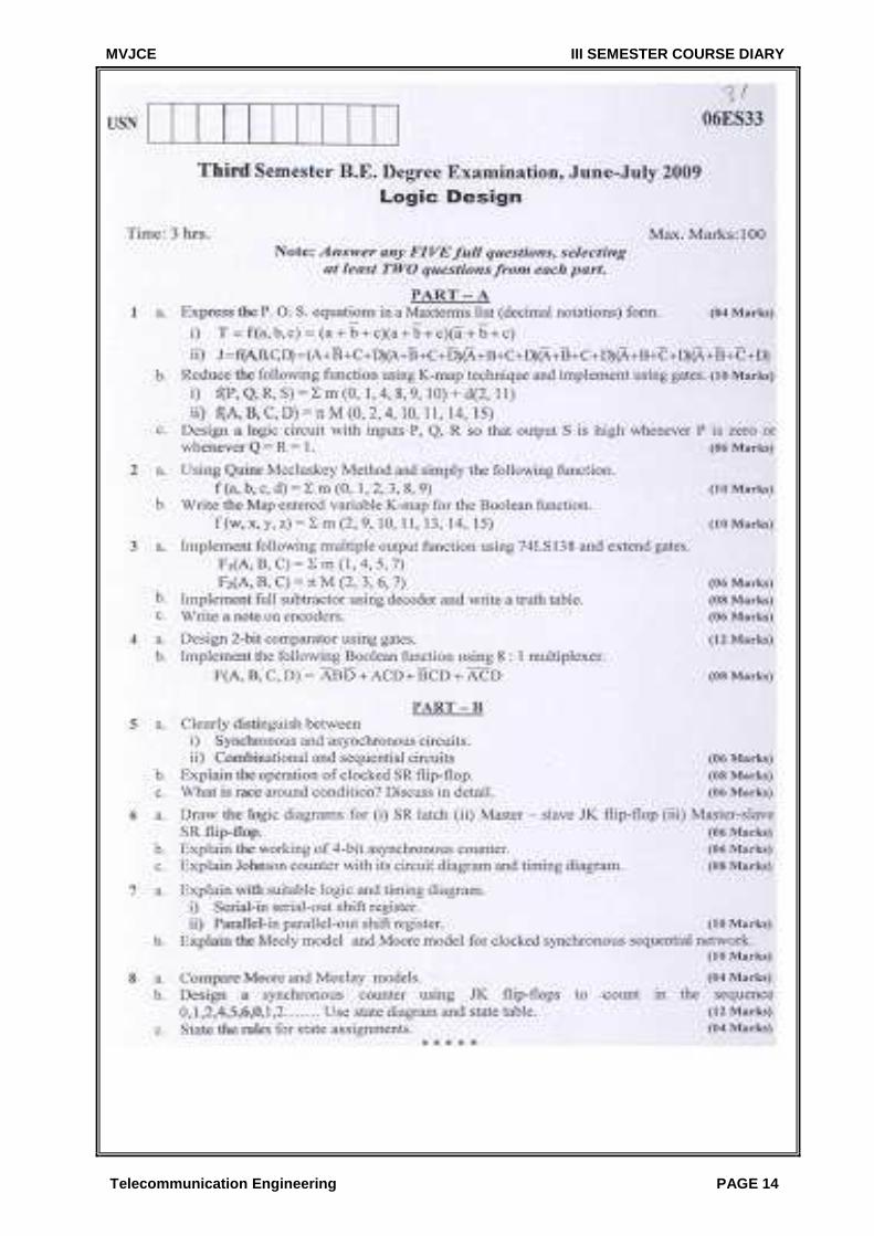
10ES33 – LOGIC DESIGN
MVJCE III SEMESTER COURSE DIARY
Telecommunication Engineering PAGE 8
SYLLABUS
Sub Code: 10ES33 I A Marks: 25 Hours / Week: 05 Exam Hours: 03 Total Hours: 62 Exam Marks: 100
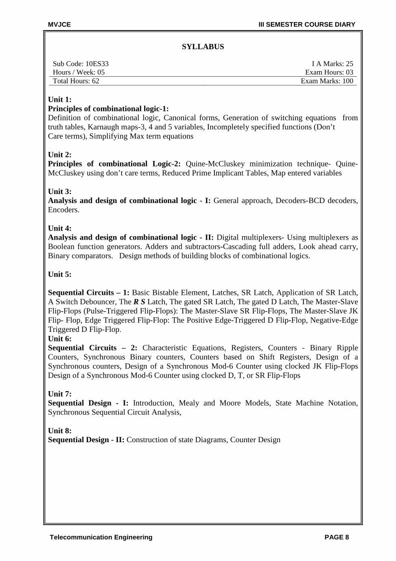
Unit 1: Principles of combinational logic-1: Definition of combinational logic, Canonical forms, Generation of switching equations from truth tables, Karnaugh maps-3, 4 and 5 variables, Incompletely specified functions (Don’t Care terms), Simplifying Max term equations Unit 2: Principles of combinational Logic-2: Quine-McCluskey minimization technique- Quine-McCluskey using don’t care terms, Reduced Prime Implicant Tables, Map entered variables Unit 3: Analysis and design of combinational logic - I: General approach, Decoders-BCD decoders, Encoders. Unit 4: Analysis and design of combinational logic - II: Digital multiplexers- Using multiplexers as Boolean function generators. Adders and subtractors-Cascading full adders, Look ahead carry, Binary comparators. Design methods of building blocks of combinational logics. Unit 5: Sequential Circuits – 1: Basic Bistable Element, Latches, SR Latch, Application of SR Latch, A Switch Debouncer, The R S Latch, The gated SR Latch, The gated D Latch, The Master-Slave Flip-Flops (Pulse-Triggered Flip-Flops): The Master-Slave SR Flip-Flops, The Master-Slave JK Flip- Flop, Edge Triggered Flip-Flop: The Positive Edge-Triggered D Flip-Flop, Negative-Edge Triggered D Flip-Flop. Unit 6: Sequential Circuits – 2: Characteristic Equations, Registers, Counters - Binary Ripple Counters, Synchronous Binary counters, Counters based on Shift Registers, Design of a Synchronous counters, Design of a Synchronous Mod-6 Counter using clocked JK Flip-Flops Design of a Synchronous Mod-6 Counter using clocked D, T, or SR Flip-Flops Unit 7: Sequential Design - I: Introduction, Mealy and Moore Models, State Machine Notation, Synchronous Sequential Circuit Analysis, Unit 8: Sequential Design - II: Construction of state Diagrams, Counter Design
MVJCE III SEMESTER COURSE DIARY
Telecommunication Engineering PAGE 9
TEXT BOOKS: 1. “Digital Logic Applications and Design”, John M Yarbrough, Thomson Learning, 2001. 2. “Digital Principles and Design “, Donald D Givone, Tata McGraw Hill Edition, 2002. REFERENCE BOOKS: 1. “Fundamentals of logic design”, Charles H Roth, Jr; Thomson Learning, 2004. 2. “Logic and computer design Fundamentals”, Mono and Kim, Pearson, Second edition, 2001. 3. “Logic Design”, Sudhakar Samuel, Pearson/Saguine, 2007
MVJ College of Engineering Department of Telecommunication
LESSON PLAN
Subject: Logic Design Subject Code: 10ES33 Total No. Of Hours –62
HOURS
TOPICS TO BE COVERED
MVJCE III SEMESTER COURSE DIARY
Telecommunication Engineering PAGE 10
HOURS
TOPICS TO BE COVERED
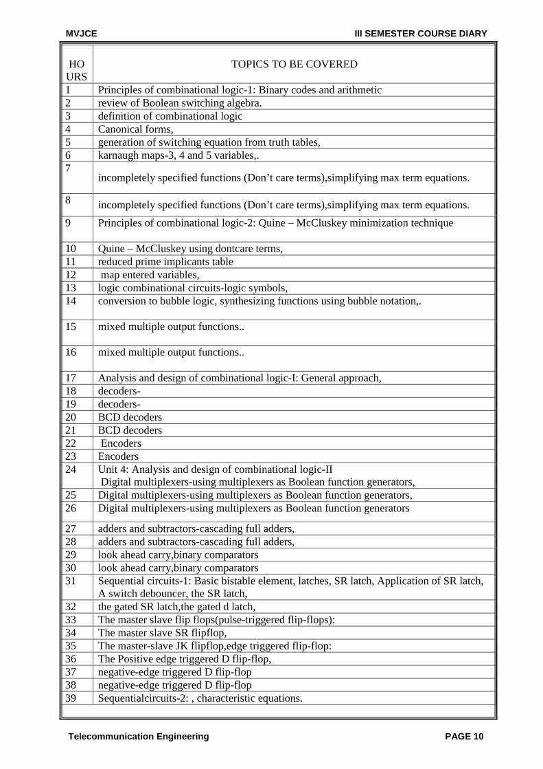
1 Principles of combinational logic-1: Binary codes and arithmetic 2 review of Boolean switching algebra. 3 definition of combinational logic 4 Canonical forms, 5 generation of switching equation from truth tables, 6 karnaugh maps-3, 4 and 5 variables,. 7
incompletely specified functions (Don’t care terms),simplifying max term equations.
8 incompletely specified functions (Don’t care terms),simplifying max term equations.
9 Principles of combinational logic-2: Quine – McCluskey minimization technique
10 Quine – McCluskey using dontcare terms, 11 reduced prime implicants table 12 map entered variables, 13 logic combinational circuits-logic symbols, 14 conversion to bubble logic, synthesizing functions using bubble notation,.
15 mixed multiple output functions..
16 mixed multiple output functions..
17 Analysis and design of combinational logic-I: General approach, 18 decoders- 19 decoders- 20 BCD decoders 21 BCD decoders 22 Encoders 23 Encoders 24 Unit 4: Analysis and design of combinational logic-II
Digital multiplexers-using multiplexers as Boolean function generators, 25 Digital multiplexers-using multiplexers as Boolean function generators, 26 Digital multiplexers-using multiplexers as Boolean function generators
27 adders and subtractors-cascading full adders, 28 adders and subtractors-cascading full adders, 29 look ahead carry,binary comparators 30 look ahead carry,binary comparators 31 Sequential circuits-1: Basic bistable element, latches, SR latch, Application of SR latch,
A switch debouncer, the SR latch, 32 the gated SR latch,the gated d latch, 33 The master slave flip flops(pulse-triggered flip-flops): 34 The master slave SR flipflop, 35 The master-slave JK flipflop,edge triggered flip-flop: 36 The Positive edge triggered D flip-flop, 37 negative-edge triggered D flip-flop 38 negative-edge triggered D flip-flop 39 Sequentialcircuits-2: , characteristic equations.
MVJCE III SEMESTER COURSE DIARY
Telecommunication Engineering PAGE 11
HOURS
TOPICS TO BE COVERED
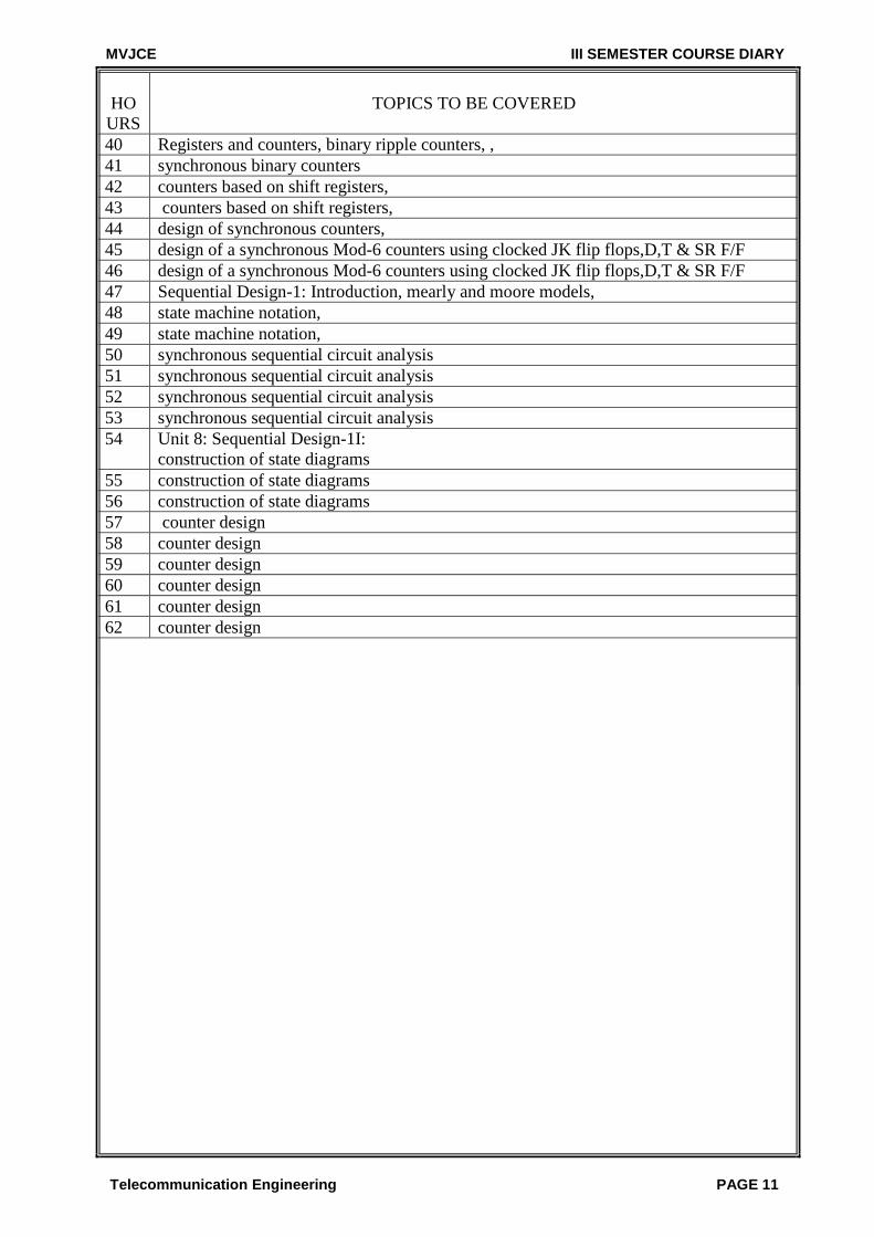
40 Registers and counters, binary ripple counters, , 41 synchronous binary counters 42 counters based on shift registers, 43 counters based on shift registers, 44 design of synchronous counters, 45 design of a synchronous Mod-6 counters using clocked JK flip flops,D,T & SR F/F 46 design of a synchronous Mod-6 counters using clocked JK flip flops,D,T & SR F/F 47 Sequential Design-1: Introduction, mearly and moore models, 48 state machine notation, 49 state machine notation, 50 synchronous sequential circuit analysis 51 synchronous sequential circuit analysis 52 synchronous sequential circuit analysis 53 synchronous sequential circuit analysis 54 Unit 8: Sequential Design-1I:
construction of state diagrams 55 construction of state diagrams 56 construction of state diagrams 57 counter design 58 counter design 59 counter design 60 counter design 61 counter design 62 counter design
MVJCE III SEMESTER COURSE DIARY
Telecommunication Engineering PAGE 12
MVJCE III SEMESTER COURSE DIARY
Telecommunication Engineering PAGE 13
MVJCE III SEMESTER COURSE DIARY
Telecommunication Engineering PAGE 14
MVJCE III SEMESTER COURSE DIARY
Telecommunication Engineering PAGE 15
10ES 34–NETWORK ANALYSIS
MVJCE III SEMESTER COURSE DIARY
Telecommunication Engineering PAGE 16
SYLLABUS
Sub Code: 10ES 34 I A Marks: 25 Hours / Week: 05 Exam Hours: 03 Total Hours: 62 Exam Marks: 100
PART – A
UNIT 1: Basic Concepts: Practical sources, Source transformations, Network reduction using Star – Delta transformation, Loop and node analysis With linearly dependent and independent sources for DC and AC networks, Concepts of super node and super mesh UNIT 2: Network Topology: Graph of a network, Concept of tree and co-tree, incidence matrix, tie -set, tie-set and cut-set schedules, Formulation of equilibrium equations in matrix form, Solution of resistive networks, Principle of duality. UNIT 3: Network Theorems – 1: Superposition, Reciprocity and Millman’s theorems UNIT 4: Network Theorems - II: Thevinin’s and Norton’s theorems; Maximum Power transfer theorem
PART – B UNIT 5: Resonant Circuits: Series and parallel resonance, frequency response of series and Parallel circuits, Q –factor, Bandwidth. UNIT 6: Transient behavior and initial conditions: Behavior of circuit elements under switching condition and their Representation, evaluation of initial and final conditions in RL, RC and RLC circuits for AC and DC excitations. UNIT 7: Laplace Transformation & Applications: Solution of networks, step, ramp and impulse responses, waveform Synthesis UNIT 8: Two port network parameters: Definition of z, y, h and transmission parameters, modeling with these parameters, relationship between parameters sets TEXT BOOKS: 1. “Network Analysis”, M. E. Van Valkenburg, PHI / Pearson Education, 3rd Edition. Reprint 2002. 2. “Networks and systems”, Roy Choudhury, 2nd edition, 2006 re-print, New Age International Publications.
REFERENCE BOOKS: 1. “Engineering Circuit Analysis”, Hayt, Kemmerly and DurbinTMH 7th Edition, 2010 2. “Basic Engineering Circuit Analysis”, J. David Irwin / R. Mark Nelms, John Wiley, 8th ed, 2006. 3.“ Fundamentals of Electric Circuits”, Charles K Alexander and Mathew N O Sadiku, Tata McGraw-Hill,3rd,2009.
MVJCE III SEMESTER COURSE DIARY
Telecommunication Engineering PAGE 17
MVJ College of Engineering Department of Telecommunication
LESSON PLAN
Subject: Network Analysis Subject code:10ES34 Total No. of Hours:62
Hours Topics to be covered
Chapter 1 – Basic Concepts
01 Network Topology, Network, Network element, Branch, Node, mesh, Circuit Elements, Energy Sources.
02 Series and parallel connection of elements. Network reduction and problem on network reduction
Series and parallel connection of elements. Network reduction and problem on network reduction
03 Network Reduction - Using Star – Delta transformation
04 Network Simplification Techniques - Introduction - Classification of Electrical Network - Circuit Elements - Energy Sources - Kirchoff’s laws - Review of loop and node - Linearly independent KVL - Linearly independent KCL
05 Solution of Networks using KVL for AC and DC 06 Solution of Networks using KCL for AC and DC 07 Source shifting problems on KCL, KVL and source shifting. Chapter 2 – Network Topology
08
Introduction to Graph theory and Network Equation - Interconnection of passive and active element constitutes an electric network. - Graph, Tree, Incidence Matrix - Linear graph for a network and its oriented graph - Planar graph, Non-planar graph, sub-graph - Rank of a graph, R = N-1 - Tree – Links / Chords,
09 Properties of trees - Incidence Matrix, Properties of Incidence Matrix - Complete Incidence Matrix - Reduced Incidence Matrix
10 Tie - Set Schedule - What do you mean by Tie-set? - How to write Tie-set matrix? - How to solve networks and obtain equilibrium equations using Tie-set schedule? - Using Loop Analysis.
11 Tie - Set Schedule - What do you mean by Tie-set? - How to write Tie-set matrix? - How to solve networks and obtain equilibrium equations using Tie-set schedule? - Using Loop Analysis.
12 Cut- Set Schedule – What do you mean by Cut-set? - How to write Cut-set matrix? - How to solve networks and obtain equilibrium equations using Cut-set schedule? - Using Nodal Analysis
13 Solving examination problems on Incidence Matrix, Tie-set and Cut-set schedule.
14 Network analysis using graph theory. Relation between branch element and loop element and branch voltage and node voltage.
15 Solving examination problems and on cut set and tie set. 16 Chapter 3 – Network Theorems
17 Superposition theorem - Explanation of the theorem - Steps to apply superposition theorem - Proof of superposition theorem
18 Problems on superposition theorem.
19 Thevenin’s theorem - Explanation of the theorem - Steps to apply Thevenin’s theorem - Proof of Thevenin’s theorem
20 Thevenin’s theorem - Explanation of the theorem - Steps to apply Thevenin’s theorem - Proof of Thevenin’s theorem
MVJCE III SEMESTER COURSE DIARY
Telecommunication Engineering PAGE 18
Hours Topics to be covered
21 Norton’s theorem - Explanation of the theorem - Steps to apply Norton’s theorem - Proof of Norton’s theorem
22 Problems on both thevinins and Norton theorem.
23 Maximum Power Transfer theorem - Explanation of the theorem - Steps to apply Maximum Power Transfer theorem - Proof of Max. Power Transfer theorem
24 Mill man’s theorem - Explanation of the theorem - Steps to apply Mill man’s theorem - Proof of Mill man’s theorem
25 Reciprocity theorem - Explanation of the theorem - Steps to apply Reciprocity theorem - Proof of Reciprocity theorem
26
Problems on reciprocity, Millman and Maximum power transfer theorems.
27 Chapter 4 – Resonant Circuits
28 Introduction - Series Resonance - Parallel Resonance - Series Resonance - Phasor diagram - Reactance Curves - Variation of impedance and admittance with frequency - Frequencies for maximum Vc and VL
29 Q Factor - Impedance of series RLC circuit in terms of Qo - Bandwidth and Selectivity - Voltage across L & C at Resonance
30 Q Factor - Impedance of series RLC circuit in terms of Qo - Bandwidth and Selectivity - Voltage across L & C at Resonance
31 Parallel Resonance - Variation of Reactance with frequency - Impedance of parallel resonant circuit in terms of Qo - Impedance of parallel resonant circuit near resonant frequency
32 Bandwidth and Selectivity-Currents in parallel resonant circuit - Relation between Ic and Il.
Chapter 5 – Transient behavior and Initial Conditions
33 Introduction - Mathematical background of differential equations - General and Particular solutions for homogenous
34 Initial conditions in network - Why study initial conditions - Initial conditions in elements
35 DC Excitation to RC series circuit - What will happen if DC excitation is given to RC circuit before and after initial conditions
36 DC Excitation to RL series circuit - What will happen if DC excitation is given to RL circuit before and after initial conditions
37 DC Excitation to RL series circuit - What will happen if DC excitation is given to RL circuit before and after initial conditions
38 DC Excitation to RLC series circuit - What will happen if DC excitation is given to RLC circuit before and after initial conditions
39 Revision - Clearing doubts on DC circuit transients
40 AC Excitation to RC series circuit - What will happen if AC excitation is given to RC circuit before and after initial conditions
41 AC Excitation to RL series circuit - What will happen if AC excitation is given to RL circuit before and after initial conditions
42 AC Excitation to RLC series circuit - What will happen if AC excitation is given to RLC circuit before and after initial conditions
43 AC Excitation to RLC series circuit - What will happen if AC excitation is given to RLC circuit before and after initial conditions
44 Revision - Clearing doubts on AC circuit transients Chapter 6 – Laplace transform and Applications
45 Introduction - Laplace transform from Fourier transform - Definition and properties of Laplace transform and Inverse Laplace transform
MVJCE III SEMESTER COURSE DIARY
Telecommunication Engineering PAGE 19
46 Theorems - Initial and Final value theorem - Shifting theorem - Convolution thm
47 Laplace transform for Standard Functions - Step function - Ramp function - Impulse function - For Periodic and Non-periodic function - Delayed functions
48 Laplace transform for Standard Functions - Step function - Ramp function - Impulse function - For Periodic and Non-periodic function - Delayed functions
49 Laplace transform for Standard Functions - Step function - Ramp function - Impulse function - For Periodic and Non-periodic function - Delayed functions
50 Network Analysis using Lap lace Transform - Single Resistor in Laplace domain - Single Capacitor in Laplace domain -
51 Single Inductor in Laplace domain - Use of convolution integral in network analysis
52 Transformed Networks and their solutions Chapter 7 – Two port Network Parameters
53 Introduction - Terminal pairs or Ports - Functions for one port and two port network - Driving point admittance - Transfer functions - Poles and Zero’s
54 Significance of location of Poles and Zero’s - Restriction of location of Poles and Zero’s in S-Plane
55 Time domain behavior from Pole-Zero plot - Determination of network function for a Two Port network
56 Time domain behavior from Pole-Zero plot - Determination of network function for a Two Port network
57 Introduction – Relationship of Two Port Variables - Characterization of linear time invariant two port network - Open circuit impedance parameters (Z-Parameters)
58 Short circuit admittance parameters (Y-Parameters) 59 Hybrid Parameters (H-Parameters) - Inverse hybrid parameters 60 ABCD Parameters/Transmission parameters 61 Relationship between parameters - Interconnection of Two Port networks 62 Revision - Clearing doubts on H,Y,Z Parameters
Signature of Staff Signature of HOD
MVJCE III SEMESTER COURSE DIARY
Telecommunication Engineering PAGE 20
MVJCE III SEMESTER COURSE DIARY
Telecommunication Engineering PAGE 21
MVJCE III SEMESTER COURSE DIARY
Telecommunication Engineering PAGE 22
QUESTION BANK
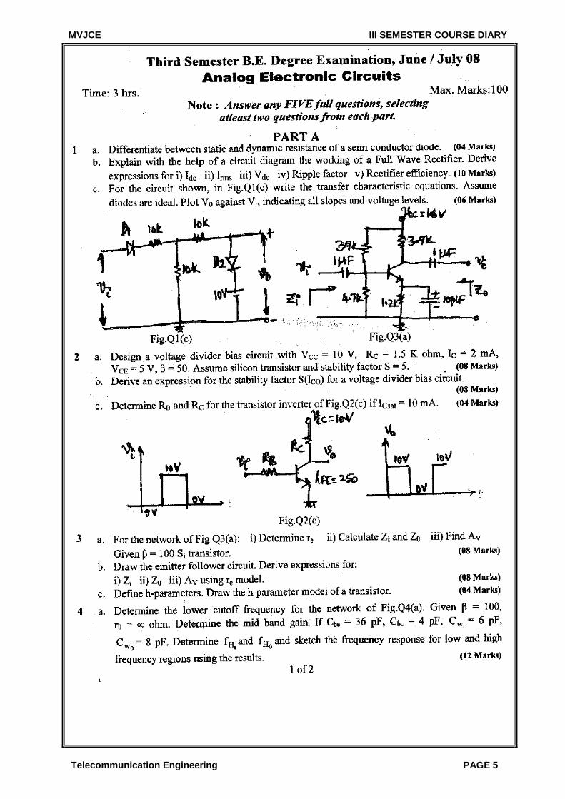
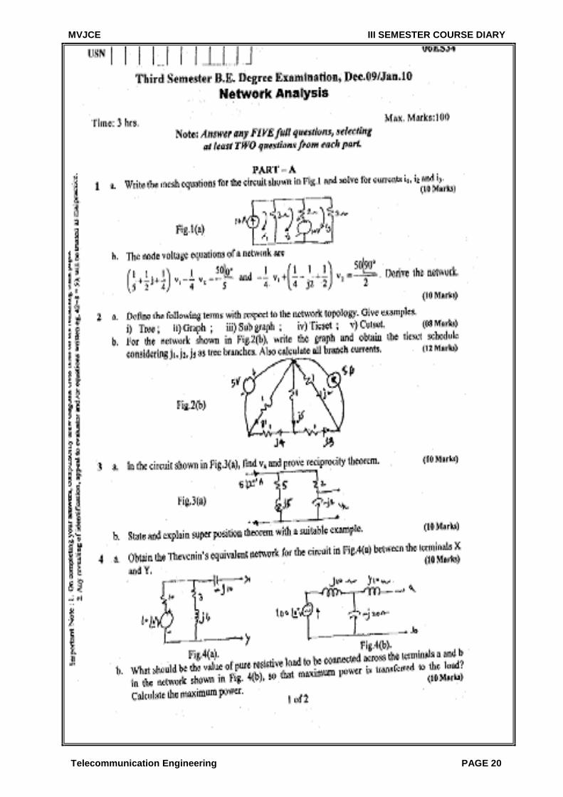
Note; Answer any five questions 1a. Develop a model equation for a general network in the form [Y][V]=[I]
Where [Y] – Admittance Matrix [V] – Node voltage Matrix [I] - Source Current Matrix (08) 1b. For the circuit shown in the fig, Determine the line currents IR , , Iy and IB using mesh
analysis (08)
Z2 = Z3 = Z1 =5∠100 V Fig 1b 1c. Explain Source transformation with suitable examples (04) 2a. Using Star- Delta transformation find RAB for the given network shown in fig (05) Fig 2a
2Ω 2Ω
2Ω
3Ω
1Ω
3Ω
1Ω
2Ω
1Ω
I2
IR
IY
Z3
I3
100∠1230 V 100∠-1230 V
Z2
Z1
IB
I1
100∠00 V
MVJCE III SEMESTER COURSE DIARY
Telecommunication Engineering PAGE 23
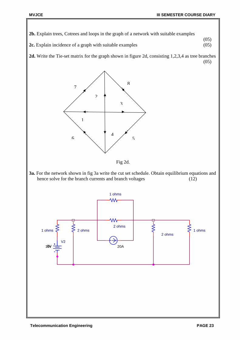
2b. Explain trees, Cotrees and loops in the graph of a network with suitable examples (05) 2c. Explain incidence of a graph with suitable examples (05) 2d. Write the Tie-set matrix for the graph shown in figure 2d, consisting 1,2,3,4 as tree branches (05)
Fig 2d. 3a. For the network shown in fig 3a write the cut set schedule. Obtain equilibrium equations and
hence solve for the branch currents and branch voltages (12) Fig 3a
8
2
1
6
7
3
4 5
1 ohms2 ohms
1 ohms 2 ohms2 ohms
1 ohms
20A10vV2
0V
MVJCE III SEMESTER COURSE DIARY
Telecommunication Engineering PAGE 24
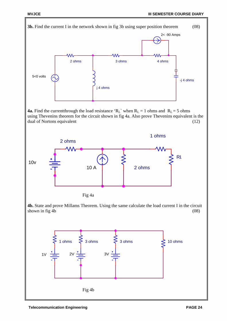
3b. Find the current I in the network shown in fig 3b using super position theorem (08) Fig 3b 4a. Find the currentthrough the load resistance ‘RL` when RL = 1 ohms and RL = 5 ohms using Thevenins theorem for the circuit shown in fig 4a. Also prove Thevenins equivalent is the dual of Nortons equivalent (12) Fig 4a 4b. State and prove Millams Theorem. Using the same calculate the load current I in the circuit shown in fig 4b (08) Fig 4b
2 ohms 4 ohms
j 4 ohms
-j 4 ohms5<0 volts
2< -90 Amps
3 ohms
2 ohms1 ohms
2 ohms
RL
10 A10v
1 ohms 3 ohms 3 ohms 10 ohms
1V 2V 3V
MVJCE III SEMESTER COURSE DIARY
Telecommunication Engineering PAGE 25
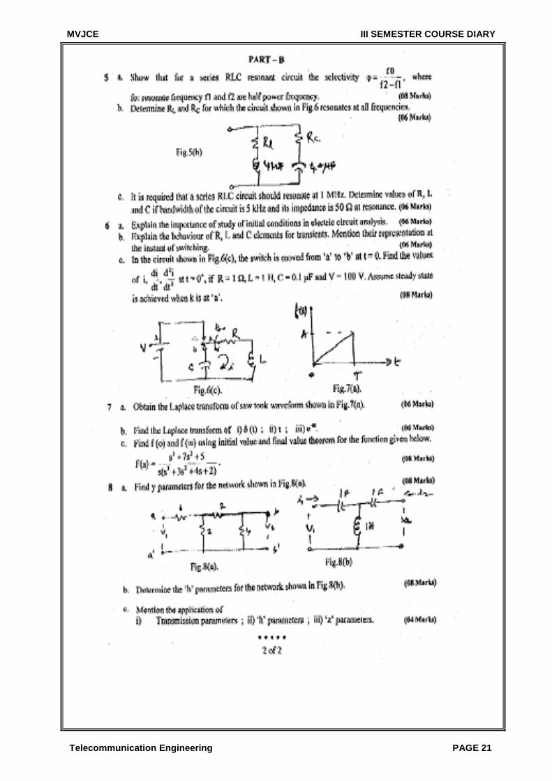
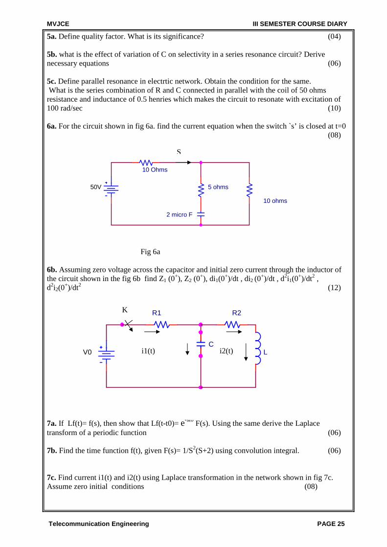
5a. Define quality factor. What is its significance? (04) 5b. what is the effect of variation of C on selectivity in a series resonance circuit? Derive necessary equations (06) 5c. Define parallel resonance in electrtic network. Obtain the condition for the same. What is the series combination of R and C connected in parallel with the coil of 50 ohms resistance and inductance of 0.5 henries which makes the circuit to resonate with excitation of 100 rad/sec (10) 6a. For the circuit shown in fig 6a. find the current equation when the switch `s’ is closed at t=0 (08) Fig 6a 6b. Assuming zero voltage across the capacitor and initial zero current through the inductor of the circuit shown in the fig 6b find Z1 (0
+), Z2 (0+), di1(0
+)/dt , di2 (0+)/dt , d2i1(0
+)/dt2 , d2i2(0
+)/dt2 (12) Fig 6b 7a. If Lf(t)= f(s), then show that Lf(t-t0)= e-st0 F(s). Using the same derive the Laplace transform of a periodic function (06) 7b. Find the time function f(t), given F(s)= 1/S2(S+2) using convolution integral. (06) 7c. Find current i1(t) and i2(t) using Laplace transformation in the network shown in fig 7c. Assume zero initial conditions (08)
10 Ohms
10 ohms
2 micro F
50V 5 ohms
S
R1 R2
LC
V0
i1(t) i2(t)
K
MVJCE III SEMESTER COURSE DIARY
Telecommunication Engineering PAGE 26
Fig 7c
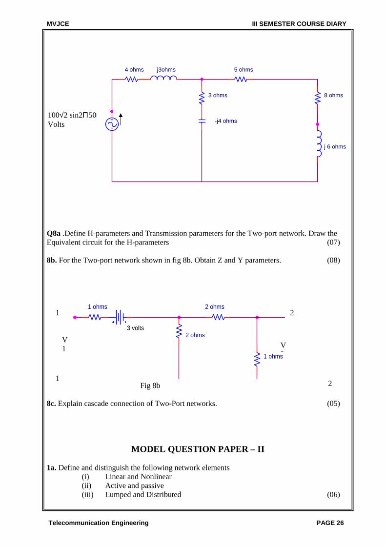
Q8a .Define H-parameters and Transmission parameters for the Two-port network. Draw the Equivalent circuit for the H-parameters (07) 8b. For the Two-port network shown in fig 8b. Obtain Z and Y parameters. (08) Fig 8b 8c. Explain cascade connection of Two-Port networks. (05)
MODEL QUESTION PAPER – II
1a. Define and distinguish the following network elements
(i) Linear and Nonlinear (ii) Active and passive (iii) Lumped and Distributed (06)
100√2 sin2Π50t Volts
4 ohms 5 ohms
8 ohms3 ohms
j3ohms
j 6 ohms
-j4 ohms
2
1 ohms 2 ohms
1 ohms
3 volts2 ohms
1
1
2
V1 V
2
MVJCE III SEMESTER COURSE DIARY
Telecommunication Engineering PAGE 27
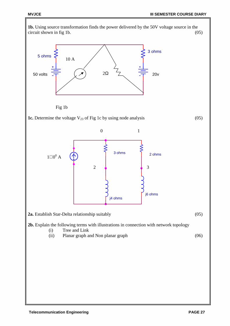
1b. Using source transformation finds the power delivered by the 50V voltage source in the circuit shown in fig 1b. (05) Fig 1b 1c. Determine the voltage V23 of Fig 1c by using node analysis (05) Fig 1c 2a. Establish Star-Delta relationship suitably (05) 2b. Explain the following terms with illustrations in connection with network topology
(i) Tree and Link (ii) Planar graph and Non planar graph (06)
1∠00 A 3 ohms 2 ohms
j4 ohmsj6 ohms
1 0
2 3
5 ohms3 ohms
50 volts 20v
2Ω
10 A
MVJCE III SEMESTER COURSE DIARY
Telecommunication Engineering PAGE 28
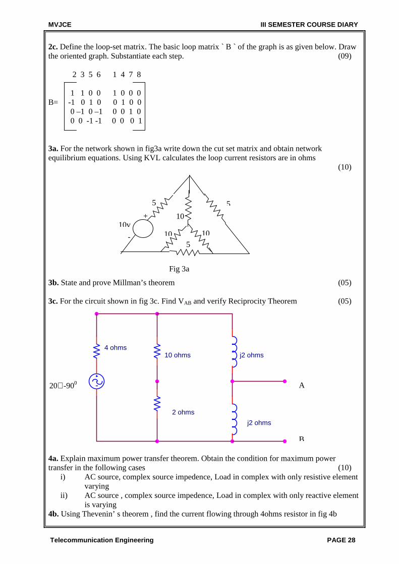
2c. Define the loop-set matrix. The basic loop matrix ` B ` of the graph is as given below. Draw the oriented graph. Substantiate each step. (09) 2 3 5 6 1 4 7 8 1 1 0 0 1 0 0 0 B= -1 0 1 0 0 1 0 0 0 –1 0 –1 0 0 1 0 0 0 -1 -1 0 0 0 1 3a. For the network shown in fig3a write down the cut set matrix and obtain network equilibrium equations. Using KVL calculates the loop current resistors are in ohms (10)
Fig 3a
3b. State and prove Millman’s theorem (05) 3c. For the circuit shown in fig 3c. Find VAB and verify Reciprocity Theorem (05) Fig 3c. 4a. Explain maximum power transfer theorem. Obtain the condition for maximum power transfer in the following cases (10)
i) AC source, complex source impedence, Load in complex with only resistive element varying
ii) AC source , complex source impedence, Load in complex with only reactive element is varying
4b. Using Thevenin’ s theorem , find the current flowing through 4ohms resistor in fig 4b
4 ohms10 ohms
2 ohms
j2 ohms
j2 ohms
20∠-900 A
B
5
5
10
10
10 -
+ 10v
5
MVJCE III SEMESTER COURSE DIARY
Telecommunication Engineering PAGE 29
(10)
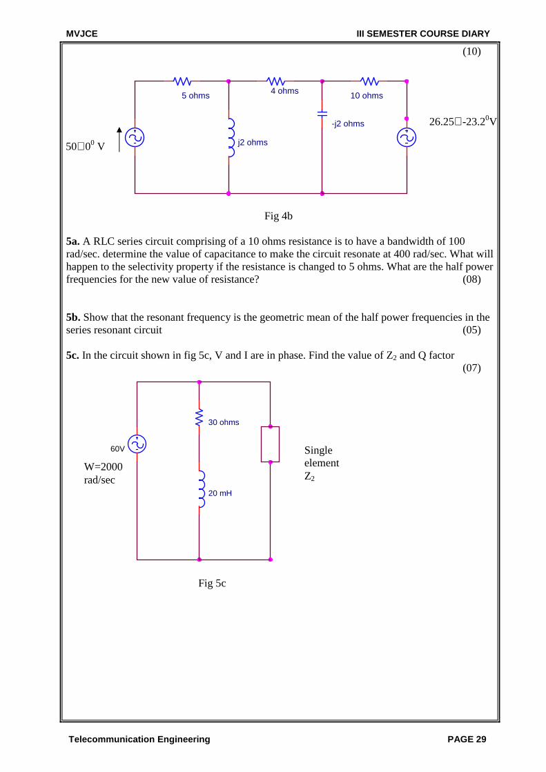
Fig 4b 5a. A RLC series circuit comprising of a 10 ohms resistance is to have a bandwidth of 100 rad/sec. determine the value of capacitance to make the circuit resonate at 400 rad/sec. What will happen to the selectivity property if the resistance is changed to 5 ohms. What are the half power frequencies for the new value of resistance? (08) 5b. Show that the resonant frequency is the geometric mean of the half power frequencies in the series resonant circuit (05) 5c. In the circuit shown in fig 5c, V and I are in phase. Find the value of Z2 and Q factor
(07) Fig 5c
5 ohms 4 ohms 10 ohms
j2 ohms
-j2 ohms
50∠00 V
26.25∠-23.20V
30 ohms
20 mH
60V
W=2000 rad/sec
Single element Z2
MVJCE III SEMESTER COURSE DIARY
Telecommunication Engineering PAGE 30
6a. Illustrate the procedure to determine the transient and steady state response of the circuit shown in fig 6a. when switch K is closed at t=0+. Assume all initial conditions are zero. Also compute di1/dt and di2/dt at t=0+ (10) Fig 6a) 6b.In the circuit shown in fig 6b. switch K is closed from 20V to 1µF at time t=0, steady state condition having been reached before switching. Find the values of i, di/dt and di2/dt2 all at t= 0+ (10)
Fig 6b. 7a. State and prove initial and final value theorems. Also find initial and final values of the following: (07) I(s) =S2+5/ S3+2S2+4S 7b.Construct the following waveform shown in fig 7b using step function and find the Laplace transform for the same, if the waveform is repeated after 4 sec. What is the Laplace transform for this periodic function (07)
Fig 7b.
R2
R1LE
C
K
i1
i2
10 ohms
1 H1micro F
20V
K
amplitude
V(t)
time 0
1v
2v
MVJCE III SEMESTER COURSE DIARY
Telecommunication Engineering PAGE 31
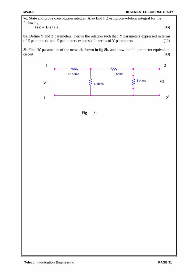
7c. State and prove convolution integral. Also find f(t) using convolution integral for the following F(s) = 1/(s+a)s (06) 8a. Define Y and Z parameters. Derive the relation such that Y parameters expressed in terms of Z parameters and Z parameters expressed in terms of Y parameters (12) 8b.Find ‘h’ parameters of the network shown in fig 8b. and draw the ‘h’ parameter equivalent circuit (08)
Fig 8b
12 ohms 3 ohms
6 ohms3 ohms
V1 V2
2
21
1
11
MVJCE III SEMESTER COURSE DIARY
Telecommunication Engineering PAGE 32
10IT 35 –ELECTRONIC INSTRUMENTATION
MVJCE III SEMESTER COURSE DIARY
Telecommunication Engineering PAGE 33
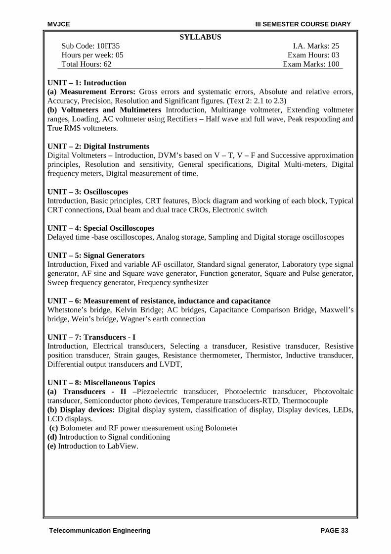
SYLLABUS Sub Code: 10IT35 I.A. Marks: 25 Hours per week: 05 Exam Hours: 03 Total Hours: 62 Exam Marks: 100
UNIT – 1: Introduction (a) Measurement Errors: Gross errors and systematic errors, Absolute and relative errors, Accuracy, Precision, Resolution and Significant figures. (Text 2: 2.1 to 2.3) (b) Voltmeters and Multimeters Introduction, Multirange voltmeter, Extending voltmeter ranges, Loading, AC voltmeter using Rectifiers – Half wave and full wave, Peak responding and True RMS voltmeters. UNIT – 2: Digital Instruments Digital Voltmeters – Introduction, DVM’s based on V – T, V – F and Successive approximation principles, Resolution and sensitivity, General specifications, Digital Multi-meters, Digital frequency meters, Digital measurement of time. UNIT – 3: Oscilloscopes Introduction, Basic principles, CRT features, Block diagram and working of each block, Typical CRT connections, Dual beam and dual trace CROs, Electronic switch UNIT – 4: Special Oscilloscopes Delayed time -base oscilloscopes, Analog storage, Sampling and Digital storage oscilloscopes UNIT – 5: Signal Generators Introduction, Fixed and variable AF oscillator, Standard signal generator, Laboratory type signal generator, AF sine and Square wave generator, Function generator, Square and Pulse generator, Sweep frequency generator, Frequency synthesizer UNIT – 6: Measurement of resistance, inductance and capacitance Whetstone’s bridge, Kelvin Bridge; AC bridges, Capacitance Comparison Bridge, Maxwell’s bridge, Wein’s bridge, Wagner’s earth connection UNIT – 7: Transducers - I Introduction, Electrical transducers, Selecting a transducer, Resistive transducer, Resistive position transducer, Strain gauges, Resistance thermometer, Thermistor, Inductive transducer, Differential output transducers and LVDT, UNIT – 8: Miscellaneous Topics (a) Transducers - II –Piezoelectric transducer, Photoelectric transducer, Photovoltaic transducer, Semiconductor photo devices, Temperature transducers-RTD, Thermocouple (b) Display devices: Digital display system, classification of display, Display devices, LEDs, LCD displays. (c) Bolometer and RF power measurement using Bolometer (d) Introduction to Signal conditioning (e) Introduction to LabView.
MVJCE III SEMESTER COURSE DIARY
Telecommunication Engineering PAGE 34
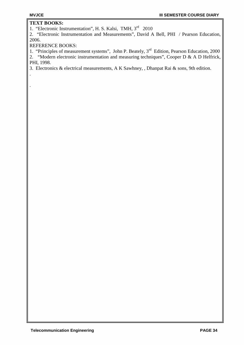
TEXT BOOKS: 1. “Electronic Instrumentation”, H. S. Kalsi, TMH, 3rd 2010 2. “Electronic Instrumentation and Measurements”, David A Bell, PHI / Pearson Education, 2006. REFERENCE BOOKS: 1. “Principles of measurement systems”, John P. Beately, 3rd Edition, Pearson Education, 2000 2. “Modern electronic instrumentation and measuring techniques”, Cooper D & A D Helfrick, PHI, 1998. 3. Electronics & electrical measurements, A K Sawhney, , Dhanpat Rai & sons, 9th edition. . .
MVJCE III SEMESTER COURSE DIARY
Telecommunication Engineering PAGE 35
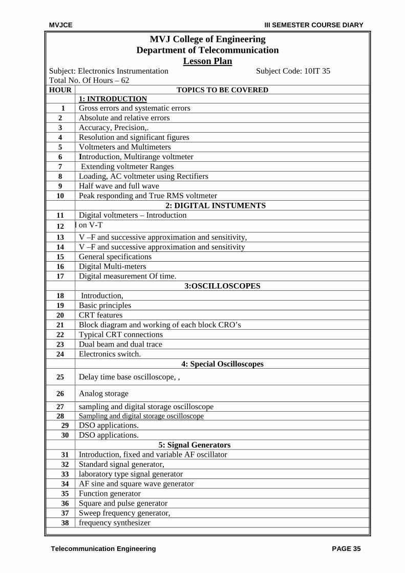
MVJ College of Engineering Department of Telecommunication
Lesson Plan Subject: Electronics Instrumentation Subject Code: 10IT 35 Total No. Of Hours – 62 HOUR TOPICS TO BE COVERED
1: INTRODUCTION 1 Gross errors and systematic errors
2 Absolute and relative errors 3 Accuracy, Precision,. 4 Resolution and significant figures 5 Voltmeters and Multimeters 6 Introduction, Multirange voltmeter 7 Extending voltmeter Ranges 8 Loading, AC voltmeter using Rectifiers 9 Half wave and full wave 10 Peak responding and True RMS voltmeter 2: DIGITAL INSTUMENTS
11 Digital voltmeters – Introduction 12 DVM’s Based on V-T
13 V –F and successive approximation and sensitivity, 14 V –F and successive approximation and sensitivity 15 General specifications 16 Digital Multi-meters 17 Digital measurement Of time. 3:OSCILLOSCOPES
18 Introduction, 19 Basic principles 20 CRT features 21 Block diagram and working of each block CRO’s 22 Typical CRT connections 23 Dual beam and dual trace 24 Electronics switch. 4: Special Oscilloscopes
25 Delay time base oscilloscope, ,
26 Analog storage
27 sampling and digital storage oscilloscope 28 Sampling and digital storage oscilloscope
29 DSO applications. 30 DSO applications.
5: Signal Generators 31 Introduction, fixed and variable AF oscillator 32 Standard signal generator, 33 laboratory type signal generator 34 AF sine and square wave generator 35 Function generator 36 Square and pulse generator 37 Sweep frequency generator, 38 frequency synthesizer
MVJCE III SEMESTER COURSE DIARY
Telecommunication Engineering PAGE 36
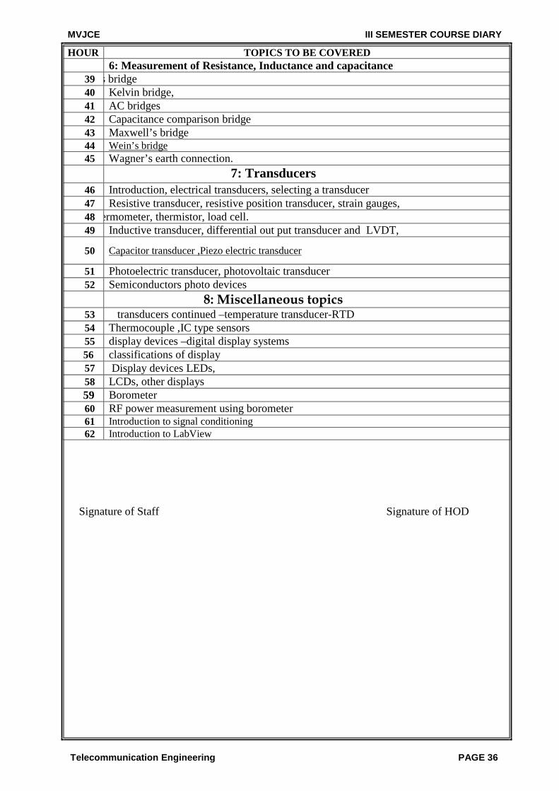
HOUR TOPICS TO BE COVERED 6: Measurement of Resistance, Inductance and capacitance 39 Wheat stone’s bridge 40 Kelvin bridge, 41 AC bridges 42 Capacitance comparison bridge 43 Maxwell’s bridge 44 Wein’s bridge 45 Wagner’s earth connection. 7: Transducers 46 Introduction, electrical transducers, selecting a transducer 47 Resistive transducer, resistive position transducer, strain gauges, 48 Resistance thermometer, thermistor, load cell. 49 Inductive transducer, differential out put transducer and LVDT,
50 Capacitor transducer ,Piezo electric transducer
51 Photoelectric transducer, photovoltaic transducer 52 Semiconductors photo devices
8: Miscellaneous topics 53 transducers continued –temperature transducer-RTD 54 Thermocouple ,IC type sensors 55 display devices –digital display systems
56 classifications of display 57 Display devices LEDs, 58 LCDs, other displays
59 Borometer 60 RF power measurement using borometer 61 Introduction to signal conditioning 62 Introduction to LabView
Signature of Staff Signature of HOD
MVJCE III SEMESTER COURSE DIARY
Telecommunication Engineering PAGE 37
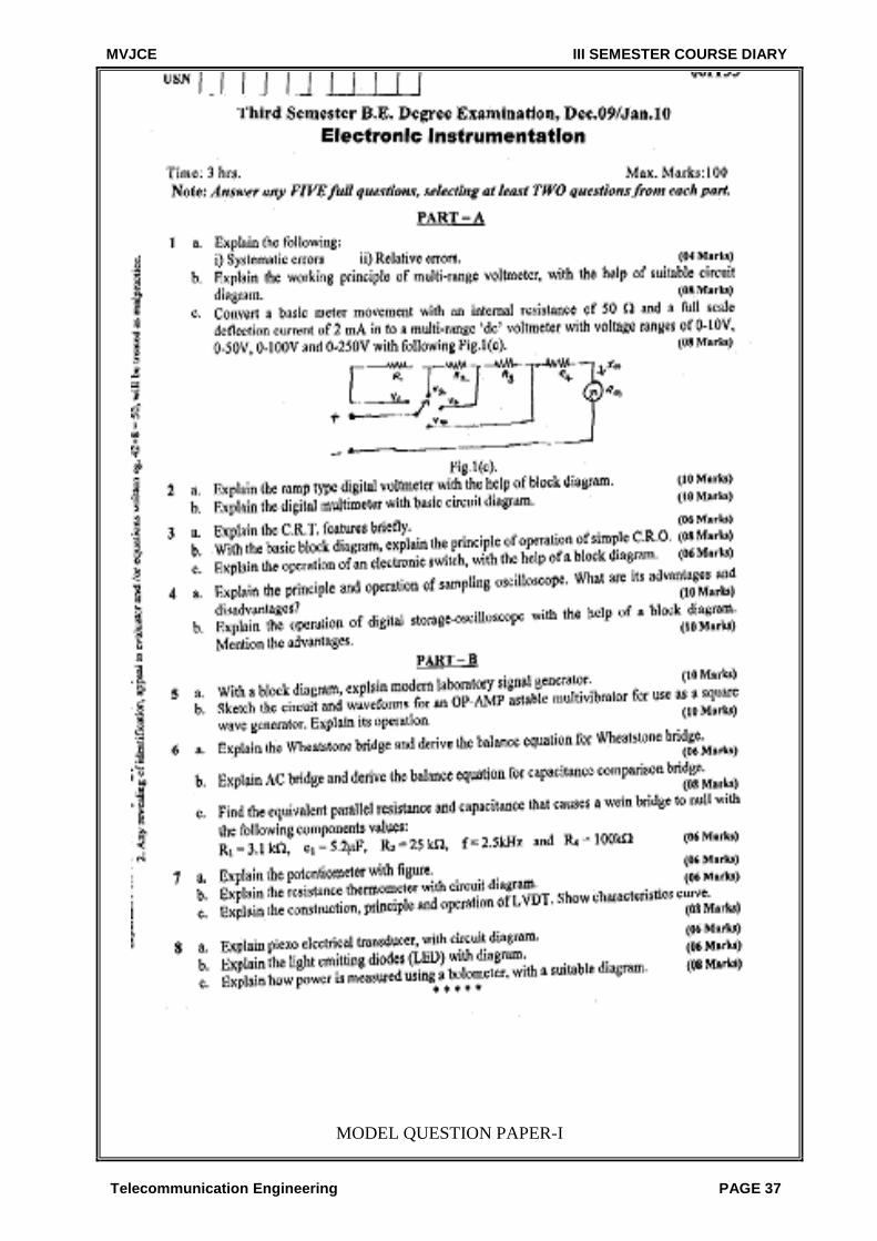
MODEL QUESTION PAPER-I
MVJCE III SEMESTER COURSE DIARY
Telecommunication Engineering PAGE 38
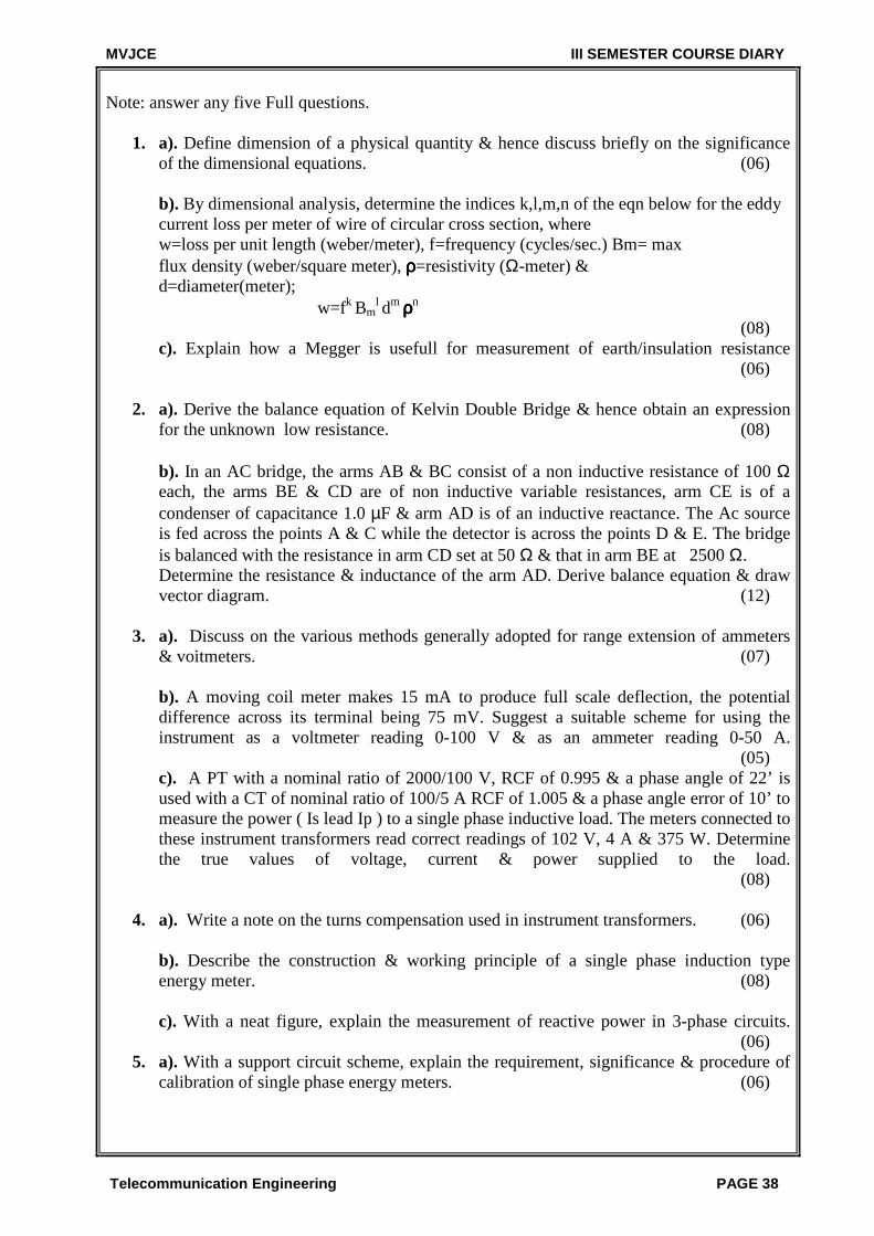
Note: answer any five Full questions.
1. a). Define dimension of a physical quantity & hence discuss briefly on the significance of the dimensional equations. (06)
b). By dimensional analysis, determine the indices k,l,m,n of the eqn below for the eddy current loss per meter of wire of circular cross section, where w=loss per unit length (weber/meter), f=frequency (cycles/sec.) Bm= max flux density (weber/square meter), ρρρρ=resistivity (Ω-meter) & d=diameter(meter);
w=fk Bml dm ρρρρn
(08) c). Explain how a Megger is usefull for measurement of earth/insulation resistance (06)
2. a). Derive the balance equation of Kelvin Double Bridge & hence obtain an expression for the unknown low resistance. (08)
b). In an AC bridge, the arms AB & BC consist of a non inductive resistance of 100 Ω each, the arms BE & CD are of non inductive variable resistances, arm CE is of a condenser of capacitance 1.0 µF & arm AD is of an inductive reactance. The Ac source is fed across the points A & C while the detector is across the points D & E. The bridge is balanced with the resistance in arm CD set at 50 Ω & that in arm BE at 2500 Ω. Determine the resistance & inductance of the arm AD. Derive balance equation & draw vector diagram. (12)
3. a). Discuss on the various methods generally adopted for range extension of ammeters
& voitmeters. (07)
b). A moving coil meter makes 15 mA to produce full scale deflection, the potential difference across its terminal being 75 mV. Suggest a suitable scheme for using the instrument as a voltmeter reading 0-100 V & as an ammeter reading 0-50 A. (05) c). A PT with a nominal ratio of 2000/100 V, RCF of 0.995 & a phase angle of 22’ is used with a CT of nominal ratio of 100/5 A RCF of 1.005 & a phase angle error of 10’ to measure the power ( Is lead Ip ) to a single phase inductive load. The meters connected to these instrument transformers read correct readings of 102 V, 4 A & 375 W. Determine the true values of voltage, current & power supplied to the load. (08)
4. a). Write a note on the turns compensation used in instrument transformers. (06)
b). Describe the construction & working principle of a single phase induction type energy meter. (08) c). With a neat figure, explain the measurement of reactive power in 3-phase circuits. (06)
5. a). With a support circuit scheme, explain the requirement, significance & procedure of calibration of single phase energy meters. (06)
MVJCE III SEMESTER COURSE DIARY
Telecommunication Engineering PAGE 39
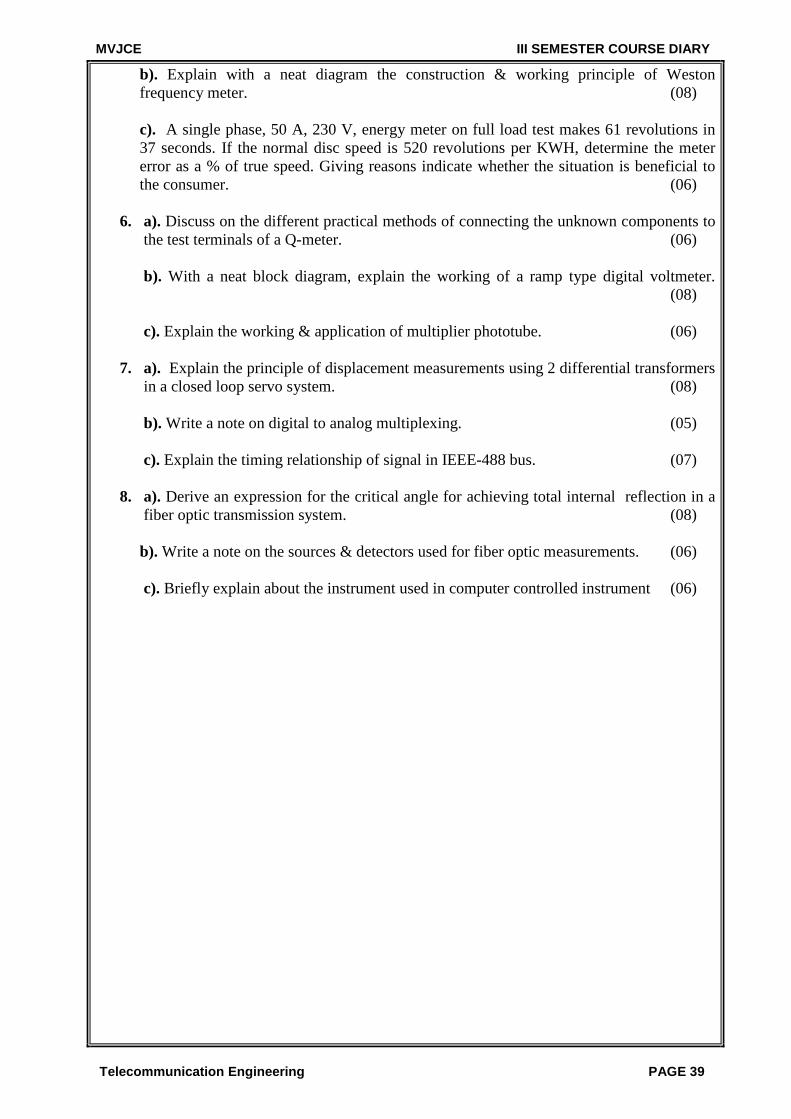
b). Explain with a neat diagram the construction & working principle of Weston frequency meter. (08)
c). A single phase, 50 A, 230 V, energy meter on full load test makes 61 revolutions in 37 seconds. If the normal disc speed is 520 revolutions per KWH, determine the meter error as a % of true speed. Giving reasons indicate whether the situation is beneficial to the consumer. (06)
6. a). Discuss on the different practical methods of connecting the unknown components to
the test terminals of a Q-meter. (06) b). With a neat block diagram, explain the working of a ramp type digital voltmeter. (08) c). Explain the working & application of multiplier phototube. (06) 7. a). Explain the principle of displacement measurements using 2 differential transformers
in a closed loop servo system. (08) b). Write a note on digital to analog multiplexing. (05) c). Explain the timing relationship of signal in IEEE-488 bus. (07) 8. a). Derive an expression for the critical angle for achieving total internal reflection in a
fiber optic transmission system. (08) b). Write a note on the sources & detectors used for fiber optic measurements. (06) c). Briefly explain about the instrument used in computer controlled instrument (06)
MVJCE III SEMESTER COURSE DIARY
Telecommunication Engineering PAGE 40
10ES36– FIELD THEORY
MVJCE III SEMESTER COURSE DIARY
Telecommunication Engineering PAGE 41
SYLLABUS
Sub Code: 10ES36 I.A. Marks: 25 Hours per week: 05 Exam Hours: 03 Total Hours: 62 Exam Marks: 100
UNIT 1: a. Coulomb’s Law and electric field intensity: Experimental law of Coulomb, Electric field intensity, Field due to continuous volume charge distribution, Field of a line charge b. Electric flux density, Gauss’ law and divergence: Electric flux density, Gauss’ law, Divergence, Maxwell’s First equation(Electrostatics), vector operator Ñ and divergence theorem UNIT 2: a. Energy and potential : Energy expended in moving a point charge in an electric field, The line integral, Definition of potential difference and Potential, The potential field of a point charge and system of charges, Potential gradient , Energy density in an electrostatic field b. Conductors, dielectrics and capacitance: Current and current density, Continuity of current, metallic conductors, Conductor properties and boundary conditions, boundary conditions for perfect Dielectrics, capacitance and examp les. UNIT 3: Poisson’s and Laplace’s equations: Derivations of Poisson’s and Laplace’s Equations, Uniqueness theorem, Examples of the solutions of Laplace’s and Poisson’s equations UNIT 4: The steady magnetic field: Biot-Savart law, Ampere’s circuital law, Curl, Stokes’ theorem, magnetic flux and flux density, scalar and Vector magnetic potentials UNIT 5: a. Magnetic forces: Force on a moving charge and differential current element, Force between differential current elements, Force and torque on a closed circuit. b. Magnetic materials and inductance: Magnetization and permeability, Magnetic boundary conditions, Magnetic circuit, Potential energy and forces on magnetic materials, Inductance and Mutual Inductance. UNIT 6: Time varying fields and Maxwell’s equations: Faraday’s law, displacement current, Maxwell’s equation in point and Integral form, retarded potentials. UNIT 7: Uniform plane wave: Wave propagation in free space and dielectrics, Poynting’s theorem and wave power, propagation in good conductors – (skin effect).
MVJCE III SEMESTER COURSE DIARY
Telecommunication Engineering PAGE 42
UNIT 8: Plane waves at boundaries and in dispersive media: Reflection of uniform plane waves at normal incidence, SWR, Plane wave propagation in general directions. TEXT BOOK: “ Engineering Electromagnetics”, William H Hayt Jr. and John A Buck, Tata McGraw-Hill, 7th edition, 2006 REFERENCE BOOKS: 1. “Electromagnetics with Applications”, John Krauss and Daniel A Fleisch, McGraw-Hill, 5th edition, 1999 2. “Electromagnetic Waves And Radiating Systems,” Edward C. Jordan and Keith G Balmain, Prentice – Hall of India / Pearson Education, 2nd edition, 1968.Reprint 2002 3. “Field and Wave Electromagnetics”, David K Cheng, Pearson Education Asia, 2nd edition, - 1989, Indian Reprint – 2001.
MVJCE III SEMESTER COURSE DIARY
Telecommunication Engineering PAGE 43
MVJ College of Engineering Department of Telecommunication
LESSON PLAN
Subject: – FIELD THEORY SUB CODE:10ES36 Total Hours: 62
Hours Topics to be covered
01 Introduction to electric fields. Fundamental relation of electrostatic field, Coulombs law.
02 Electric field intensity, Experiment law of coulomb, Relation between Electric field intensity & Electric field, Field due to Point charge.
03 Electric field intensity, Experiment law of coulomb, Relation between Electric field intensity & Electric field, Field due to Point charge.
04 Field due to continuous volume charge, line charge and sheet charge. Simple problems relating electric field, electric field intensity.
05 Electric flux density, Relation between vector D&E and Gauss law. 06 Application of Gauss law
Field at a point due to an infinite line charge of uniform liner charge density, Field at a point due to a spherical shell of charge.
07 Vector operator v, Divergence and Gauss divergence theorem. 08 Vector operator v, Divergence and Gauss divergence theorem.
09 Energy and potential, Expression for energy expended in moving a point charge in an electric field. Problems on the same.
10 Definition of potential difference and potential 11 Expression for Electrostatic potential due to point and a system of charges. 12 Expression for Electrostatic potential due to point and a system of charges. 13 Expression for potential gradient and energy density in an electric field. 14 Solving problems on potential gradient and energy density. 15 Definition for current and Current density and deriving expression for the same.
Problems on current density. 16 Obtaining an expression for continuity of current and definition for metallic
conductors. 17 Obtaining an expression for continuity of current and definition for metallic
conductors. 18 Conductor properties and boundary conditions. 19 Boundary conditions for perfect dielectrics, capacitance and examples. 20 Poisson and Laplace’s Equations 21 Uniqueness theorem. 22 Uniqueness theorem. 23 Examples of the solutions of Laplace’s and Poisson’s equations. 24 Introduction to magnetostatics and Biot-Savart law. 25 Amperes law, proof of Amperes circuital law. 26 Amperes law, proof of Amperes circuital law. 27 Solving problems based on Amperes circuital law. 28 Curl, Stoke’s Theorem. Problems on the same. 29 Definition for magnetic flux and flux density. 30 Scalar and Vector magnetic potential
MVJCE III SEMESTER COURSE DIARY
Telecommunication Engineering PAGE 44
31 Scalar and Vector magnetic potential 32 Problems on flux and flux density, scalar and vector magnetic potential. 33 Force on a moving charge and differential current element. 34 Force between differential current elements. 35 Force between differential current elements. 36 Force and torque on a closed circuit. 37 Magnetization and permeability 38 Magnetic boundary conditions, magnetic circuit 39 Magnetic boundary conditions, magnetic circuit 40 Energy & forces on magnetic materials, self-inductance. 41 Solving problems based on Magnetostatics. 42 Faraday’s law and displacement current. 43 Maxwell’s Equation: Modification of the Static field equation for time varying
fields 44 Maxwell’s equation in differential form. 45 Maxwell’s equation in Integral form and word statement form, retarded potential. 46 Problems on Maxwell’s equation. 47 Introduction to electromagnetic waves and wave propagation 48 Electric and Magnetic wave equation 49 Defining Uniform plane waves.
Relation between E and H for a uniform plane wave. 50 Defining Uniform plane waves.
Relation between E and H for a uniform plane wave. 51 Solution of wave equation for a uniform wave in (a) Conducting medium &
(b) in low –loss dielectric. 52 Solution of wave equation for a uniform wave in perfect dielectric 53 Wave propagation in free space and dielectrics. 54 Introduction to Poynting vector and Power flow. Power considerations. 55 Propagation in good conductors (skin effect), wave polarization. 56 Derivation of propagation constant, attenuation constant, phase velocity and
wavelength. 57 Reflection of uniform plane waves at the surface of the conductors and dielectrics-
Brewster angle 58 Reflection of uniform plane waves in dispersive media. 59 Reflection of uniform plane waves at normal incidence, SWR. 60 Reflection of uniform plane waves at oblique incidence, Brewster’s angle. 61 Problems on uniform plane waves and polarization. 62 Problems on pointing vector and power flow.
Signature of Staff Signature of HOD
MVJCE III SEMESTER COURSE DIARY
Telecommunication Engineering PAGE 45
MVJCE III SEMESTER COURSE DIARY
Telecommunication Engineering PAGE 46
MVJCE III SEMESTER COURSE DIARY
Telecommunication Engineering PAGE 47
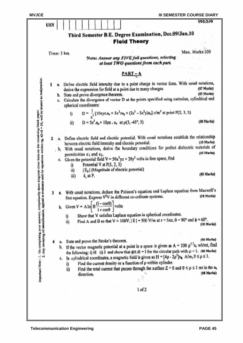
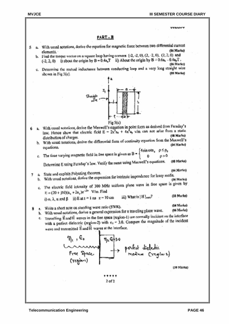
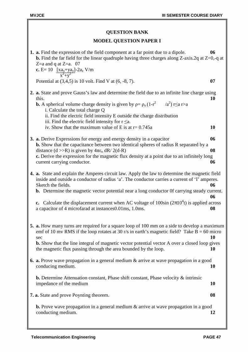
QUESTION BANK
MODEL QUESTION PAPER I 1. a. Find the expression of the field component at a far point due to a dipole. 06
b. Find the far field for the linear quadruple having three charges along Z-axis.2q at Z=0,-q at Z=a and q at Z=a. 07
c. E= 10 [xax+yay]-2az V/m x2+y2 Potential at (3,4,5) is 10 volt. Find V at (6, -8, 7). 07 2. a. State and prove Gauss’s law and determine the field due to an infinite line charge using
this. 10 b. A spherical volume charge density is given by ρ= ρo (1-r2 /a2) r≤a r>a
i. Calculate the total charge Q ii. Find the electric field intensity E outside the charge distribution iii. Find the electric field intensity for r ≤a. iv. Show that the maximum value of E is at r= 0.745a 10
3. a. Derive Expressions for energy and energy density in a capacitor 06
b. Show that the capacitance between two identical spheres of radius R separated by a distance (d >>R) is given by 4πεo dR/ 2(d-R) 08 c. Derive the expression for the magnetic flux density at a point due to an infinitely long current carrying conductor. 06
4. a. State and explain the Amperes circuit law. Apply the law to determine the magnetic field
inside and outside a conductor of radius ‘a’. The conductor carries a current of ‘I’ amperes. Sketch the fields. 06 b. Determine the magnetic vector potential near a long conductor 0f carrying steady current. 06 c. Calculate the displacement current when AC voltage of 100sin (2π104t) is applied across a capacitor of 4 microfarad at instances0.01ms, 1.0ms. 08
5. a. How many turns are required for a square loop of 100 mm on a side to develop a maximum
emf of 10 mv RMS if the loop rotates at 30 r/s in earth’s magnetic field? Take B = 60 micro sec 10 b. Show that the line integral of magnetic vector potential vector A over a closed loop gives the magnetic flux passing through the area bounded by the loop. 10
6. a. Prove wave propagation in a general medium & arrive at wave propagation in a good
conducing medium. 10
b. Determine Attenuation constant, Phase shift constant, Phase velocity & intrinsic impedance of the medium 10
7. a. State and prove Poynting theorem. 08
b. Prove wave propagation in a general medium & arrive at wave propagation in a good conducting medium. 12
MVJCE III SEMESTER COURSE DIARY
Telecommunication Engineering PAGE 48
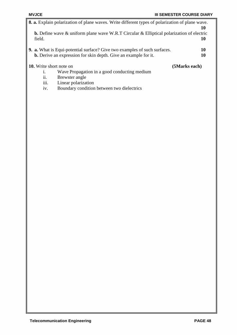
8. a. Explain polarization of plane waves. Write different types of polarization of plane wave. 10
b. Define wave & uniform plane wave W.R.T Circular & Elliptical polarization of electric field. 10
9. a. What is Equi-potential surface? Give two examples of such surfaces. 10 b. Derive an expression for skin depth. Give an example for it. 10 10. Write short note on (5Marks each)
i. Wave Propagation in a good conducting medium ii. Brewster angle iii. Linear polarization iv. Boundary condition between two dielectrics
MVJCE III SEMESTER COURSE DIARY
Telecommunication Engineering PAGE 49
QUESTION BANK
MODEL QUESTION PAPER II 1. (a) Define the following.
i) Electric field intensity. ii) Electric scalar potential. (4 marks)
(b) Volume charge density is located in free space as ρv=2e^-1000r nc/m^3 for 0< r< 1mm, and ρv = 0 elsewhere.
i) Find the total charge enclosed by the spherical surface r = 1mm. ii) By using Gauss’s law, calculate the value of Dr on the surface r = 1mm. (10 marks)
(c) Derive an expression for the relationship between electric field intensity, E and electric scalar potential, V. (6 marks)
2. (a) Calculate the divergence of D at the point specified if
(i) D=1/z2[10xyzax +5x2zay +(2z3-5x2y)az] at P[-2,3,5] (ii) D=5z2ap+10ρzaz at P [3, -45,5] (iii) D=2rsinθ sinΦ ar+rcosθ sinΦ aθ +r cosΦ aΦ at P [3,45, -45] (9 marks)
(b) Derive an expression for Gauss Law in differential form. (5 marks) (c) Discuss the boundary conditions on E and D at the boundary between two dielectrics. (6 marks) 3. (a) Given the potential field V=[ Ap4 + Bp-4] sin4 ρ
(i) Show that (ii) Select A and B so that V=100 volts and |E|=500V/m at P(ρ=1,Φ=22.5 ,z=2)
(10 marks) (b) Show that the energy density in an electrostatic field is given by ω=1/2εE2 J/m3 (6 marks) (c) Explain Biot-Savart law. (4 marks) 4 (a) Show that in a parallel plate capacitor subjected to a time –changing field, the
displacement current in the dielectric must be equal to conduction current in the wire. (6 marks) (b) Show that J=δ ρ v/ δt where ρv=volume charge density in c/m3. (6 marks) (c) Given the field H=20ρ2 aΦ A/m.
(i) Determine the current density J. (ii) Integrate J over the circular surface ρ=1,0<Φ<2π, z=0, to determine the total
current passing through that surface in the az direction. (8 marks) 5. (a) Show that the line integral of magnetic vector potential around a closed path must be equal to the flux passing through the area bounded by the closed path. (6 marks)
(b) Derive an expression for Maxwell’s Equation in vector differential form for time changing fields, starting from Faraday-Lenz’s law. (7marks)
(c) Assume A=50ρ2az ωb/m in a certain region of free space. Find H and B. (7 marks)
MVJCE III SEMESTER COURSE DIARY
Telecommunication Engineering PAGE 50
6. (a) Discuss the wave propagation of a uniform plane wave in the following: (i) Good dielectric medium. (ii) Good conducting medium. (b) Wet, marshy soil is characterized by
σ=10^-2 s/m, εr=15, and µr=1. At the frequencies 60Hz, 1MHz, 100MHz and 10 GHz, indicate whether the soil may be considered a conductor, a dielectric or neither.
(10 marks) 7. (a) State and prove Poynting’s Theorem . (10 marks) (b) Show that a uniform plane wave propagating in free space is transverse in nature. (6 marks) (c) Show that the wave impedance of free space is Zo=377Ω. (4 marks) 8. Write short notes on the following:
(i) Brewster angle. (ii) Ampere’s circuit law. (iii) Gauss law. (iv) Linear and Circular polarization.
(5*4=20 marks)
MVJCE III SEMESTER COURSE DIARY
Telecommunication Engineering PAGE 51
10ESL37 – ANALOG ELECTRONICS LAB
MVJCE III SEMESTER COURSE DIARY
Telecommunication Engineering PAGE 52
SYLLABUS
Sub Code: 10ESL37 I.A. Marks: 25 Hours per week: 03 Exam Hours: 03 Total Hours: 42 Exam Marks: 50
NOTE: Use the Discrete components to test the circuits. LabView can be used for the verification and testing along with the above. 1. Wiring of RC coupled Single stage FET & BJT amplifier and determination of the gain- frequency response, input and output impedances. 2. Wiring of BJT Darlington Emitter follower with and without bootstrapping and determination of the gain, input and output impedances (Single circuit) (One Experiment) 3. Wiring of a two stage BJT Voltage series feed back amplifier and determination of the gain, Frequency response, input and output impedances with and without feedback (One Experiment) 4. Wiring and Testing for the performance of BJT-RC Phase shift Oscillator for f0 ≤ 10 KHz 5. Testing for the performance of BJT – Hartley & Colpitts Oscillators for RF range f0 ≥100KHz. 6. Testing for the performance of BJT -Crystal Oscillator for f0 > 100 KHz 7 Testing of Diode clipping (Single/Double ended) circuits for peak clipping, peak detection 8. Testing of Clamping circuits: positive clamping /negative clamping. 9. Testing of a transformer less Class – B push pull power amplifier and determination of its conversion efficiency. 10. Testing of Half wave, Full wave and Bridge Rectifier circuits with and without Capacitor filter. Determination of ripple factor, regulation and efficiency 11. Verification of Thevinin’s Theorem and Maximum Power Transfer theorem for DC Circuits. 12. Characteristics of Series and Parallel resonant circuits.
MVJCE III SEMESTER COURSE DIARY
Telecommunication Engineering PAGE 53
LESSON PLAN Hours / Week: 3
IA Marks:25 Total Hours:42
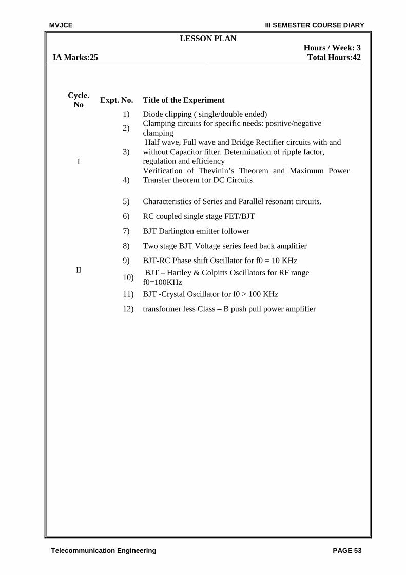
Cycle. No Expt. No. Title of the Experiment
I
1) Diode clipping ( single/double ended)
2) Clamping circuits for specific needs: positive/negative clamping
3) Half wave, Full wave and Bridge Rectifier circuits with and without Capacitor filter. Determination of ripple factor, regulation and efficiency
4) Verification of Thevinin’s Theorem and Maximum Power Transfer theorem for DC Circuits.
5) Characteristics of Series and Parallel resonant circuits.
6) RC coupled single stage FET/BJT
II
7) BJT Darlington emitter follower
8) Two stage BJT Voltage series feed back amplifier
9) BJT-RC Phase shift Oscillator for f0 = 10 KHz
10) BJT – Hartley & Colpitts Oscillators for RF range f0=100KHz
11) BJT -Crystal Oscillator for f0 > 100 KHz
12) transformer less Class – B push pull power amplifier
MVJCE III SEMESTER COURSE DIARY
Telecommunication Engineering PAGE 54
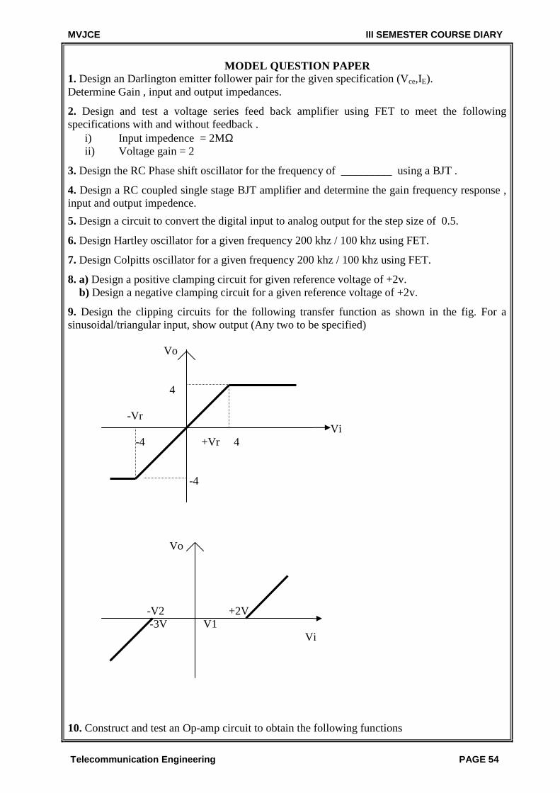
MODEL QUESTION PAPER
1. Design an Darlington emitter follower pair for the given specification (Vce,IE). Determine Gain , input and output impedances.
2. Design and test a voltage series feed back amplifier using FET to meet the following specifications with and without feedback .
i) Input impedence = 2MΩ ii) Voltage gain = 2
3. Design the RC Phase shift oscillator for the frequency of _________ using a BJT .
4. Design a RC coupled single stage BJT amplifier and determine the gain frequency response , input and output impedence.
5. Design a circuit to convert the digital input to analog output for the step size of 0.5.
6. Design Hartley oscillator for a given frequency 200 khz / 100 khz using FET.
7. Design Colpitts oscillator for a given frequency 200 khz / 100 khz using FET.
8. a) Design a positive clamping circuit for given reference voltage of +2v. b) Design a negative clamping circuit for a given reference voltage of +2v.
9. Design the clipping circuits for the following transfer function as shown in the fig. For a sinusoidal/triangular input, show output (Any two to be specified) Vo 4 -Vr Vi -4 +Vr 4 -4 Vo -V2 +2V -3V V1 Vi 10. Construct and test an Op-amp circuit to obtain the following functions
MVJCE III SEMESTER COURSE DIARY
Telecommunication Engineering PAGE 55
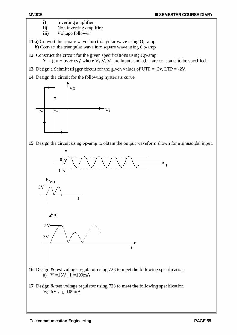
i) Inverting amplifier ii) Non inverting amplifier iii) Voltage follower
11.a) Convert the square wave into triangular wave using Op-amp b) Convert the triangular wave into square wave using Op-amp
12. Construct the circuit for the given specifications using Op-amp Y= -(av1+ bv2+ cv3) where V1,V2,V3 are inputs and a,b,c are constants to be specified.
13. Design a Schmitt trigger circuit for the given values of UTP =+2v, LTP = -2V.
14. Design the circuit for the following hysterisis curve Vo -3 -1 Vi 15. Design the circuit using op-amp to obtain the output waveform shown for a sinusoidal input. 0.5 t -0.5 Vo 5V t Vo 5V 3V t 16. Design & test voltage regulator using 723 to meet the following specification
a) V0=15V , IL=100mA
17. Design & test voltage regulator using 723 to meet the following specification V0=5V , IL=100mA
MVJCE III SEMESTER COURSE DIARY
Telecommunication Engineering PAGE 56
VIVA QUESTIONS
1. What is breakdown voltage in diodes? 2. What is cut-in voltage in diodes? 3. What are static and dynamic resistances of a diode? 4. What is reverse resistance of a diode? 5. What are the values of reverse resistances of different diodes? 6. What are the values of Cut-in Voltages of Si and Ge diode? 7. What are the values of Zener break down voltages of different Zener diode? 8. What is Zener breakdown voltage? 9. What is Avalanche breakdown voltage? 10. What are the differences between Avalanche and Zener Breakdown? 11. What is regulator? 12. What is Series Voltage Regulator? 13. What is Shunt Voltage Regulator? 14. What are the differences between Series and Shunt Voltage Regulator? 15. Define Stability factor 16. Define Regulation factor 17. What is the difference between AC and DC 18. What is rectifier? 19. What are different types of rectifier? 20. What is filter? 21. What are the different types of filter? 22. What is BJT? 23. What are the biasing techniques in CB / CE / CC mode? 24. What are the different types of configuration? 25. What are the h-parameters? 26. What are active, saturation and cutoff region? 27. What are the values of h-parameters in CE, CB and CC configuration? 28. What is the relation between α and β? 29. Define β and α. 30. Define the various regions in output characteristics in CE mode. 31. What is FET? 32. What are the differences between BJT and FET? 33. What is JFET? 34. What are the differences between UJT and BJT? 35. What is negative resistance? 36. What are KCL and KVL laws? 37. What is active element and give examples 38. What is passive element and give examples 39. What are the differences between active and passive elements? 40. What is voltage source? 41. What is current source? 42. What is the difference between dependent and independent sources? 43. Define bandwidth 44. Define half power frequencies 45. Why should we take –3dB to find the cutoff frequencies? 46. What is frequency response? 47. How will you convert amplitude in dB? 48. What are the differences between Series and Parallel Resonance? 49. What is RC Coupling?
MVJCE III SEMESTER COURSE DIARY
Telecommunication Engineering PAGE 57
50. What are the pros and cons of RC Coupling? 51. What are the applications of RC Coupling? 52. What is emitter follower? 53. What are the values of h-parameter in CC configurations? 54. Why is the output equal to input amplitude? 55. What are the applications of emitter follower? 56. What is the advantage of Darlington Emitter Follower over conventional 57. Emitter Follower Circuit. 58. What is the input & output impedances of Darlington Emitter Follower 59. What is the stability factor for Darlington Emitter Follower 60. What is the purpose of using Voltage series feedback amplifier? 61. State Barkheusan criterion 62. Why BJT is called current controlled device. 63. What are the other names of cut off frequencies? 64. If bandwidth is very high what is the Q –factor of an amplifier. 65. What is meant by resonant frequency? 66. What are the classifications of tuned amplifier? 67. What is the frequency range of a Hartley & collpits oscillator? 68. What are the applications of clampers & clippers? 69. What are the different types of biasing techniques. 70. What are the uses of coupling & by-pass capacitors. 71. What is the gain Band width product of an amplifier. Is it a variable or constant? 72. Why FET is called as an voltage controlled device. 73. Why Band width increases in Negative feed back amplifiers.

MVJCE III SEMESTER COURSE DIARY
Telecommunication Engineering PAGE 58
10ESL38 – LOGIC DESIGN LAB
MVJCE III SEMESTER COURSE DIARY
Telecommunication Engineering PAGE 59
SYLLABUS
Sub Code: 10ESL38 I.A. Marks: 25 Hours per week: 03 Exam Hours: 03 Total Hours: 42 Exam Marks: 50
NOTE: Use discrete components to test and verify the logic gates. LabView can be used for designing the gates along with the above. 1. Simplification, realization of Boolean expressions using logic gates/Universal gates. 2. Realization of Half/Full adder and Half/Full Subtractors using logic gates. 3. (i) Realization of parallel adder/Subtractors using 7483 chip (ii) BCD to Excess-3 code conversion and vice versa. 4. Realization of Binary to Gray code conversion and vice versa 5. MUX/DEMUX – use of 74153, 74139 for arithmetic circuits and code converter. 6. Realization of One/Two bit comparator and study of 7485 magnitude comparator. 7. Use of a) Decoder chip to drive LED display and b) Priority encoder. 8. Truth table verification of Flip-Flops: (i) JK Master slave (ii) T type and (iii) D type. 9. Realization of 3 bit counters as a sequential circuit and MOD – N counter design (7476, 7490, 74192, 74193). 10. Shift left; Shift right, SIPO, SISO, PISO, PIPO operations using 74S95. 11. Wiring and testing Ring counter/Johnson counter. 12. Wiring and testing of Sequence generator.
MVJCE III SEMESTER COURSE DIARY
Telecommunication Engineering PAGE 60
LESSON PLAN
SUB CODE:10ESL38 Hours / Week: 3 IA Marks:25 Total Hours:42
S. No. Topic to be covered
CYCLE I
1. Simplification, Realization of Boolean expressions using LOGIC gates / UNIVERSAL gates.
2. Realization of half/full adder and half/full subtractor using logic gates.
3. (i) Realization of parallel adder /subtractor using 7483 chip
(ii) BCD to Ex-3 code conversion & vice versa.
4. Realization of binary to gray code converter and vice versa .
5. MUX/DEMUX use of 74153,74139 for arithmetic circuits and code converter.
CYCLE II 6. Realization of one/two bit comparator & study of 7485 magnitude comparator.
7. Use of a) decoder chip to drive LED/LCD display and b) priority encoder.
8. Truth table verification of flip-flops (i) JK master slave (ii) T-type and (iii) D type.
9. Realization of 3-bit counters as a sequential circuit & mod-N counter design
(7476,7490,74192,74193)
10. Shift left, shift right, SIPO, SISO, PISO, PIPO operations using 7495.
11. Design and testing of ring counter/Johnson counter.
CYCLE III 12. Design of a sequence generator.
13. Design and testing of astable and mono-stable circuits using 555 timer.
14. Programming a RAM (2114).
MVJCE III SEMESTER COURSE DIARY
Telecommunication Engineering PAGE 61
VIVA QUESTION
1. What is Number System? Classify 2. Define Base of a number or Radix of a number system. 3. What is logic gate? Classify 4. Why NAND and NOR are called as Universal gates. 5. What is the difference between Binary addition and Boolean addition 6. What is the difference between postulate and Law? 7. What is Idempotent law? 8. Define truth table. 9. What is the need for simplification of Boolean expression? 10. What are the methods followed to simplify a given Boolean expression. 11. Which is the best method to perform simplification. 12. Using K-map, to haw many variables maximum can be simplified. 13. Define cell. 14. What is the difference between Prime implicants and essential prime implicants? 15. Difference between Minterm and Maxterm. 16. What is SOP and POS 17. In K-Map what type of coding is used? Why other codes are not used. 18. What do you mean by ORing of AND terms and ANDing of OR terms 19. Realize the XNOR function using only XOR gates. 20. What do π and Σ indicate. 21. How do you convert SOP into POS and vice versa 22. Does NAND gate obey the commutative, associative and distributive laws? Justify your
answer with Boolean equation. 23. Define the function of half adder, Full adder, half subtractor, and full Subtractor. 24. What is the difference between carry and overflow. 25. What is the function of Parallel adder and subtractor? 26. Give the pin configuration of IC 7483. 27. What is the need for complements? 28. Classify the types of complements. 29. The 10’s and 9’s complement are performed over ------------------- numbers and 1’s & 2’s
complements are performed over ---------------------- numbers. 30. How the two’s complement operation is achieved using IC 7483. 31. What is the need for XOR gates in Parallel adder and subtractor? 32. What are the conditions required to perform Parallel addition, 1’s complement parallel
subtraction, and 2’s complement parallel subtraction. 33. What is the largest decimal number that can be added with a parallel adder consisting of
four full adders? 34. To perform addition of two 6-bit numbers, we need a parallel adder having ---------- full adder circuits 35. Can addition of two BCD numbers be performed using IC 7483? If yes, what are the
changes to be made in the circuit? 36. While adding two BCD numbers, if the sum is not a BCD number, what is to be done? 37. What is the reason for adding only 6 and not any other number to the sum of BCD
number? 38. Is it possible to perform the addition of XS3 codes using IC 7483? 39. What is code conversion? 40. Explain the need for code conversion. 41. What are the steps involved to convert a binary number into a Gray Code? 42. What are the steps involved to convert a Gray number into a binary Code? 43. Is gray code a weighted code?
MVJCE III SEMESTER COURSE DIARY
Telecommunication Engineering PAGE 62
44. What is weighted code? Give examples 45. What is Non – weighted codes, give example? 46. What are reflected codes give examples? 47. What are self-complementary codes give examples? 48. What is BCD code? 49. Where are BCD codes used? 50. What was the need for binary number system? Give its advantages over others. 51. How are XS3 codes derived? 52. Define the function of Multiplier. 53. For a 16: 1 MUX, How many AND gates and select lines are needed. 54. What is the need for select lines or control lines 55. Give the relationship between number of input lines and number of select lines 56. To construct a 32:1 MUX how many 4:1 MUX is required. 57. Give some practical applications of Multiplexers. 58. Define the function of Demultiplexer. 59. What is the need for ENABLE input in DEMUX. 60. When does a DEMUX act as a decoder? What is the condition? 61. Give some practical applications of DEMUX. 62. How do you design any code converters using DEMUX IC. 63. Give the pin configuration of IC 74139 and IC 74153. 64. What is the function of comparator? 65. How can we compare any 2 bit binary numbers? 66. Is it possible to compare 2 bit binary number using IC 7483? If yes, how? 67. How do you compare 4 bit binary number 68. What is a magnitude comparator? 69. We can divide a number into two parts. What are they? 70. If a number is a positive number, then sign bit is ----------------- and a number if negative,
then sign bit is ---------------------. 71. What is magnitude of a number? 72. What is meant by cascading inputs? 73. Define Logic 1 and logic 0? 74. Let A be a 2 bit number and B be another 2 bit number, if A > B, then Cout = ------ and S
= ----------, if A < B, then Cout = ---------- and S = -------------, and if A = B, then Cout = ---------- and S = -------------.
75. Is it possible to perform comparison of two, 8-bit number using magnitude comparator? 76. Where are the comparators used? 77. What is a Flip-flop? 78. What is the difference between a flip-flop & latch? 79. How J-k flip-flop can be converted into T & D types? 80. What is the difference between Synchronous and Asynchronous clock pulse. 81. How to design a Mod-N counter? 82. How addition and subtraction is done in a parallel adder circuits. 83. Explain the design for a Sequence Generator if the sequence given is ………………... 84. What is the difference between a sequence generator and PRBS? 85. Give the difference between sequential and combinational circuit. 86. What is a shift register? 87. What are the different modes of operation in a shift register? 88. What is the function of mode-control pin? 89. What is the difference between common cathode configuration and common anode
configuration? 90. Give the difference between LED and LCD. 91. How does an LED work? 92. What is meant by active low and active High?
MVJCE III SEMESTER COURSE DIARY
Telecommunication Engineering PAGE 63
93. What does Pull-up resistor or current – limiting resistor, mean? 94. Why R is chosen as 330Ω? 95. What is the function of a decoder? 96. Give the pin configuration of decoder chip? 97. What is the function of RBO, RB1 and LT? 98. What is an Encoder? 99. What is priority encoder? 100. Give the difference between encoder and priority encoder?
101. What is the need for inverter in the priority encoder circuit? 102. Is AND gate equivalent to series switching circuit? 103. What are bubbled gates? 104. ------------------- Gate is also called all – or - nothing gate. 103.------------------- Gate is also called any – or – all gate. 104.Define byte, nibble and bit? 105.What do the following indicate – a bubble at input end and a bubble at output end? 106. What are the types of Multivibrator? 107. What is the other name of Astable Multivibrator? 108. How to change the duty cycle of an Astable Multivibrator of an output Frequency?


![Eee-III-Analog Electronic Ckts [10es32]-Notes](https://img.pdfslide.us/doc/110x75/577cd5561a28ab9e789a820d/eee-iii-analog-electronic-ckts-10es32-notes.jpg)
![Eee-III-Analog Electronic Ckts [10es32]-Solution](https://img.pdfslide.us/doc/110x75/5529d0b54a7959fa768b45d8/eee-iii-analog-electronic-ckts-10es32-solution.jpg)