Embed Size (px)
Citation preview
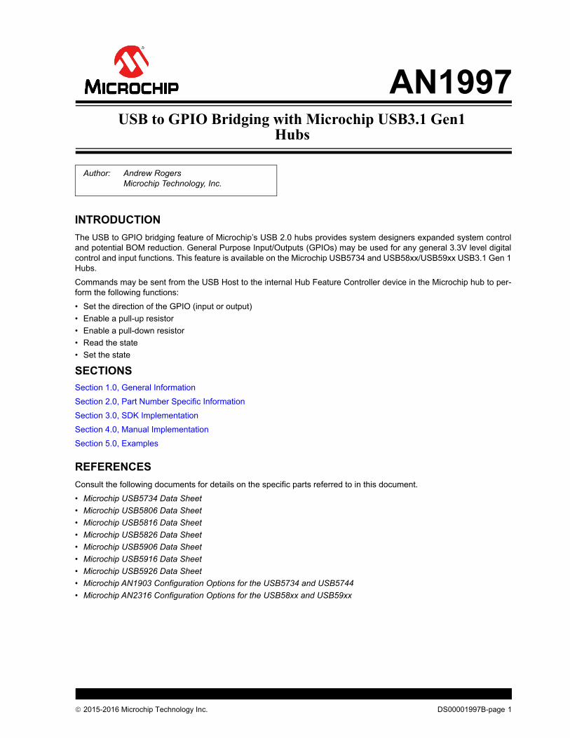
AN1997USB to GPIO Bridging with Microchip USB3.1 Gen1
Hubs
INTRODUCTION
The USB to GPIO bridging feature of Microchip’s USB 2.0 hubs provides system designers expanded system control and potential BOM reduction. General Purpose Input/Outputs (GPIOs) may be used for any general 3.3V level digital control and input functions. This feature is available on the Microchip USB5734 and USB58xx/USB59xx USB3.1 Gen 1 Hubs.
Commands may be sent from the USB Host to the internal Hub Feature Controller device in the Microchip hub to per-form the following functions:
• Set the direction of the GPIO (input or output)
• Enable a pull-up resistor
• Enable a pull-down resistor
• Read the state
• Set the state
SECTIONS
Section 1.0, General Information
Section 2.0, Part Number Specific Information
Section 3.0, SDK Implementation
Section 4.0, Manual Implementation
Section 5.0, Examples
REFERENCES
Consult the following documents for details on the specific parts referred to in this document.
• Microchip USB5734 Data Sheet
• Microchip USB5806 Data Sheet
• Microchip USB5816 Data Sheet
• Microchip USB5826 Data Sheet
• Microchip USB5906 Data Sheet
• Microchip USB5916 Data Sheet
• Microchip USB5926 Data Sheet
• Microchip AN1903 Configuration Options for the USB5734 and USB5744
• Microchip AN2316 Configuration Options for the USB58xx and USB59xx
Author: Andrew RogersMicrochip Technology, Inc.
2015-2016 Microchip Technology Inc. DS00001997B-page 1
AN1997
1.0 GENERAL INFORMATION
Microchip hub USB Bridging features in Microchip hubs work via host commands sent to a Hub Feature Controller embedded within the hub located on an additional internal USB port. In order for the bridging features to work correctly, this internal Hub Feature Controller must be enabled by default. Table 1 provides details on default Hub Feature Con-troller setters by device.
TABLE 1: DEFAULT SETTINGS FOR THE HUB FEATURE CONTROLLER ENABLE
Part Number Part SummaryHub Feature Controller Default
Setting
USB5734 4-Port USB3.1 Gen 1 Hub Enabled by default
USB5806 6-Port USB3.1 Gen1 Hub Enabled by default
USB5816 6-Port USB3.1 Gen1 Hub with Type-C™ Support on 1 Downstream Port
Enabled by default
USB5826 6-Port USB3.1 Gen1 Hub with Type-C Support on 2 Downstream Ports
Enabled by default
USB5906 6-Port USB3.1 Gen1 Hub with Type-C Support on the Upstream Port
Enabled by default
USB5916 6-Port USB3.1 Gen1 Hub with Type-C Support on the Upstream Port and 1 Downstream Port
Enabled by default
USB5926 6-Port USB3.1 Gen1 Hub with Type-C Support on the Upstream Port and 2 Downstream Ports
Enabled by default
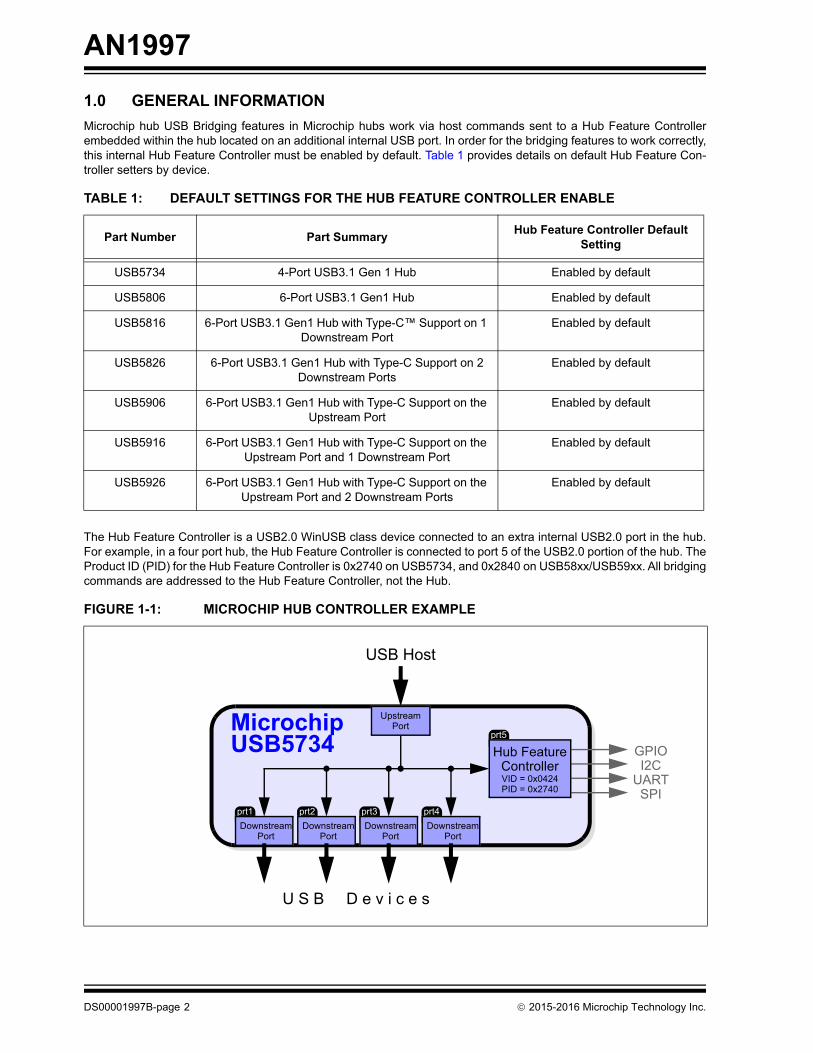
The Hub Feature Controller is a USB2.0 WinUSB class device connected to an extra internal USB2.0 port in the hub. For example, in a four port hub, the Hub Feature Controller is connected to port 5 of the USB2.0 portion of the hub. The Product ID (PID) for the Hub Feature Controller is 0x2740 on USB5734, and 0x2840 on USB58xx/USB59xx. All bridging commands are addressed to the Hub Feature Controller, not the Hub.
FIGURE 1-1: MICROCHIP HUB CONTROLLER EXAMPLE
USB Host
MicrochipUSB5734 GPIO
I2CUARTSPI
prt4prt1 prt2 prt3
prt5
UpstreamPort
Hub FeatureController
DownstreamPort
DownstreamPort
DownstreamPort
DownstreamPort
U S B D e v i c e s
VID = 0x0424PID = 0x2740
DS00001997B-page 2 2015-2016 Microchip Technology Inc.
AN1997
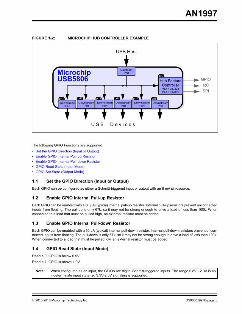
FIGURE 1-2: MICROCHIP HUB CONTROLLER EXAMPLE
USB Host
MicrochipUSB5806 GPIO
I2C
SPI
prt5prt2 prt3 prt4
prt7
UpstreamPort
Hub FeatureController
DownstreamPort
DownstreamPort
DownstreamPort
DownstreamPort
U S B D e v i c e s
VID = 0x0424PID = 0x2840
prt1
DownstreamPort
prt6
DownstreamPort
The following GPIO Functions are supported:
• Set the GPIO Direction (Input or Output)
• Enable GPIO Internal Pull-up Resistor
• Enable GPIO Internal Pull-down Resistor
• GPIO Read State (Input Mode)
• GPIO Set State (Output Mode)
1.1 Set the GPIO Direction (Input or Output)
Each GPIO can be configured as either a Schmitt-triggered input or output with an 8 mA sink/source.
1.2 Enable GPIO Internal Pull-up Resistor
Each GPIO can be enabled with a 50 μA (typical) internal pull-up resistor. Internal pull-up resistors prevent unconnected inputs from floating. The pull-up is only 67k, so it may not be strong enough to drive a load of less than 100k. When connected to a load that must be pulled high, an external resistor must be added.
1.3 Enable GPIO Internal Pull-down Resistor
Each GPIO can be enabled with a 50 μA (typical) internal pull-down resistor. Internal pull-down resistors prevent uncon-nected inputs from floating. The pull-down is only 67k, so it may not be strong enough to drive a load of less than 100k. When connected to a load that must be pulled low, an external resistor must be added.
1.4 GPIO Read State (Input Mode)
Read a 0: GPIO is below 0.9V
Read a 1: GPIO is above 1.9V
Note: When configured as an input, the GPIOs are digital Schmitt-triggered inputs. The range 0.8V - 2.0V is an indeterminate input state, so 3.3V-2.5V signaling is supported.
2015-2016 Microchip Technology Inc. DS00001997B-page 3
AN1997
1.5 GPIO Set State (Output Mode)
Set to 0: GPIO Drives to 0.0V. When driven low, an 8 mA sink is enabled driving the pin to 0.4V or lower.
Set to 1: GPIO Drives to 3.3V. When driven high, an 8 mA source is enabled driving the pin to VDD33 - 0.4V or higher.
DS00001997B-page 4 2015-2016 Microchip Technology Inc.
AN1997
2.0 PART NUMBER SPECIFIC INFORMATION
2.1 Part Summary
Table 2 summarizes the total number of available GPIOs by part number. Many of the GPIOs on the hub are only avail-able after configuration. The following methods may be used to configure the hub:
• ProTouch: If configuring via internal One-Time Programmable (OTP) memory, or if configuring via SPI EEPROM with a base firmware file.
• SMBus/I2C Configuration: If using an embedded SoC/I2C EEPROM to configure the hub at each start-up/reset.
• Pin Strapping: Many of the GPIOs are made available by specific pin strapping or by simply not populating a SPI EEPROM device.
TABLE 2: GPIO AVAILABILITY SUMMARY
USB5734 USB5806 USB5816 USB5826 USB5906 USB5916 USB5926
GPIOS Available By Default 7 0 4 3 4 3 2
Total Available GPIOs 16 14 10 9 10 9 8
2015-2016 Microchip Technology Inc. DS00001997B-page 5
AN1997
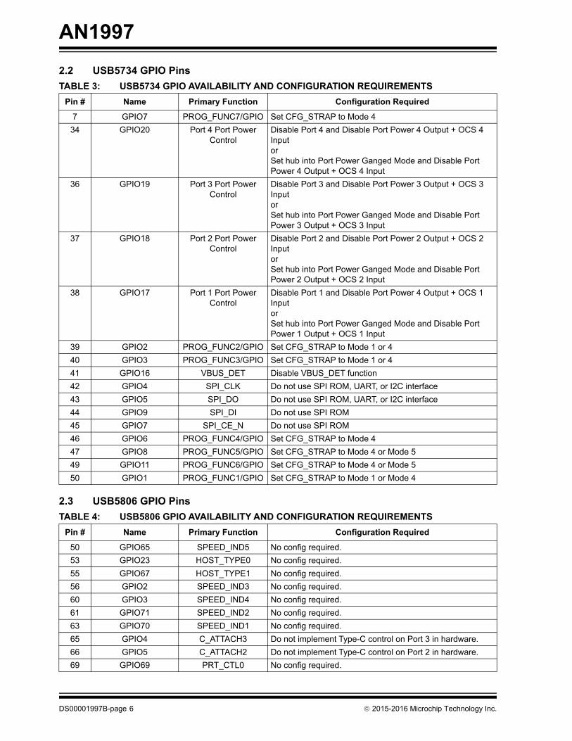
2.2 USB5734 GPIO Pins
TABLE 3: USB5734 GPIO AVAILABILITY AND CONFIGURATION REQUIREMENTS
Pin # Name Primary Function Configuration Required
7 GPIO7 PROG_FUNC7/GPIO Set CFG_STRAP to Mode 4
34 GPIO20 Port 4 Port Power Control
Disable Port 4 and Disable Port Power 4 Output + OCS 4 InputorSet hub into Port Power Ganged Mode and Disable Port Power 4 Output + OCS 4 Input
36 GPIO19 Port 3 Port Power Control
Disable Port 3 and Disable Port Power 3 Output + OCS 3 InputorSet hub into Port Power Ganged Mode and Disable Port Power 3 Output + OCS 3 Input
37 GPIO18 Port 2 Port Power Control
Disable Port 2 and Disable Port Power 2 Output + OCS 2 InputorSet hub into Port Power Ganged Mode and Disable Port Power 2 Output + OCS 2 Input
38 GPIO17 Port 1 Port Power Control
Disable Port 1 and Disable Port Power 4 Output + OCS 1 InputorSet hub into Port Power Ganged Mode and Disable Port Power 1 Output + OCS 1 Input
39 GPIO2 PROG_FUNC2/GPIO Set CFG_STRAP to Mode 1 or 4
40 GPIO3 PROG_FUNC3/GPIO Set CFG_STRAP to Mode 1 or 4
41 GPIO16 VBUS_DET Disable VBUS_DET function
42 GPIO4 SPI_CLK Do not use SPI ROM, UART, or I2C interface
43 GPIO5 SPI_DO Do not use SPI ROM, UART, or I2C interface
44 GPIO9 SPI_DI Do not use SPI ROM
45 GPIO7 SPI_CE_N Do not use SPI ROM
46 GPIO6 PROG_FUNC4/GPIO Set CFG_STRAP to Mode 4
47 GPIO8 PROG_FUNC5/GPIO Set CFG_STRAP to Mode 4 or Mode 5
49 GPIO11 PROG_FUNC6/GPIO Set CFG_STRAP to Mode 4 or Mode 5
50 GPIO1 PROG_FUNC1/GPIO Set CFG_STRAP to Mode 1 or Mode 4
2.3 USB5806 GPIO Pins
TABLE 4: USB5806 GPIO AVAILABILITY AND CONFIGURATION REQUIREMENTS
Pin # Name Primary Function Configuration Required
50 GPIO65 SPEED_IND5 No config required.
53 GPIO23 HOST_TYPE0 No config required.
55 GPIO67 HOST_TYPE1 No config required.
56 GPIO2 SPEED_IND3 No config required.
60 GPIO3 SPEED_IND4 No config required.
61 GPIO71 SPEED_IND2 No config required.
63 GPIO70 SPEED_IND1 No config required.
65 GPIO4 C_ATTACH3 Do not implement Type-C control on Port 3 in hardware.
66 GPIO5 C_ATTACH2 Do not implement Type-C control on Port 2 in hardware.
69 GPIO69 PRT_CTL0 No config required.
DS00001997B-page 6 2015-2016 Microchip Technology Inc.
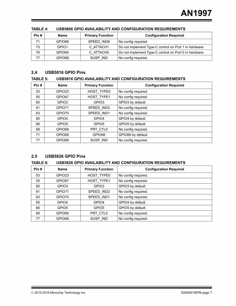
AN1997
2.4 USB5816 GPIO Pins
TABLE 5: USB5816 GPIO AVAILABILITY AND CONFIGURATION REQUIREMENTS
Pin # Name Primary Function Configuration Required
53 GPIO23 HOST_TYPE0 No config required.
55 GPIO67 HOST_TYPE1 No config required.
60 GPIO3 GPIO3 GPIO3 by default.
61 GPIO71 SPEED_IND2 No config required.
63 GPIO70 SPEED_IND1 No config required.
65 GPIO4 GPIO4 GPIO4 by default.
66 GPIO5 GPIO5 GPIO5 by default.
69 GPIO69 PRT_CTL0 No config required.
71 GPIO66 GPIO66 GPIO66 by default.
77 GPIO68 SUSP_IND No config required.
2.5 USB5826 GPIO Pins
TABLE 6: USB5826 GPIO AVAILABILITY AND CONFIGURATION REQUIREMENTS
Pin # Name Primary Function Configuration Required
53 GPIO23 HOST_TYPE0 No config required.
55 GPIO67 HOST_TYPE1 No config required.
60 GPIO3 GPIO3 GPIO3 by default.
61 GPIO71 SPEED_IND2 No config required.
63 GPIO70 SPEED_IND1 No config required.
65 GPIO4 GPIO4 GPIO4 by default.
66 GPIO5 GPIO5 GPIO5 by default.
69 GPIO69 PRT_CTL0 No config required.
77 GPIO68 SUSP_IND No config required.
71 GPIO66 SPEED_IND6 No config required.
73 GPIO1 C_ATTACH1 Do not implement Type-C control on Port 1 in hardware.
76 GPIO64 C_ATTACH0 Do not implement Type-C control on Port 0 in hardware.
77 GPIO68 SUSP_IND No config required.
TABLE 4: USB5806 GPIO AVAILABILITY AND CONFIGURATION REQUIREMENTS
Pin # Name Primary Function Configuration Required
2015-2016 Microchip Technology Inc. DS00001997B-page 7
AN1997
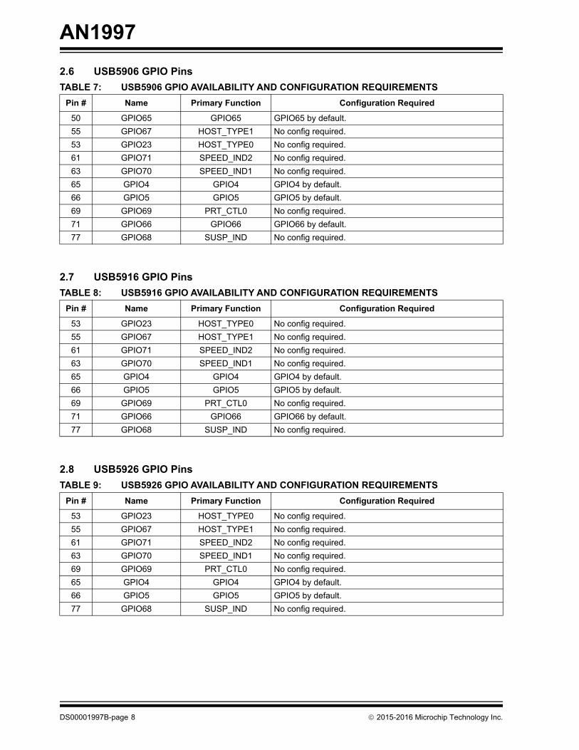
2.6 USB5906 GPIO Pins
TABLE 7: USB5906 GPIO AVAILABILITY AND CONFIGURATION REQUIREMENTS
Pin # Name Primary Function Configuration Required
50 GPIO65 GPIO65 GPIO65 by default.
55 GPIO67 HOST_TYPE1 No config required.
53 GPIO23 HOST_TYPE0 No config required.
61 GPIO71 SPEED_IND2 No config required.
63 GPIO70 SPEED_IND1 No config required.
65 GPIO4 GPIO4 GPIO4 by default.
66 GPIO5 GPIO5 GPIO5 by default.
69 GPIO69 PRT_CTL0 No config required.
71 GPIO66 GPIO66 GPIO66 by default.
77 GPIO68 SUSP_IND No config required.
2.7 USB5916 GPIO Pins
TABLE 8: USB5916 GPIO AVAILABILITY AND CONFIGURATION REQUIREMENTS
Pin # Name Primary Function Configuration Required
53 GPIO23 HOST_TYPE0 No config required.
55 GPIO67 HOST_TYPE1 No config required.
61 GPIO71 SPEED_IND2 No config required.
63 GPIO70 SPEED_IND1 No config required.
65 GPIO4 GPIO4 GPIO4 by default.
66 GPIO5 GPIO5 GPIO5 by default.
69 GPIO69 PRT_CTL0 No config required.
71 GPIO66 GPIO66 GPIO66 by default.
77 GPIO68 SUSP_IND No config required.
2.8 USB5926 GPIO Pins
TABLE 9: USB5926 GPIO AVAILABILITY AND CONFIGURATION REQUIREMENTS
Pin # Name Primary Function Configuration Required
53 GPIO23 HOST_TYPE0 No config required.
55 GPIO67 HOST_TYPE1 No config required.
61 GPIO71 SPEED_IND2 No config required.
63 GPIO70 SPEED_IND1 No config required.
69 GPIO69 PRT_CTL0 No config required.
65 GPIO4 GPIO4 GPIO4 by default.
66 GPIO5 GPIO5 GPIO5 by default.
77 GPIO68 SUSP_IND No config required.
DS00001997B-page 8 2015-2016 Microchip Technology Inc.
AN1997
3.0 SDK IMPLEMENTATION
The simplest method for implementing the USB to GPIO bridging functions is to use the publicly available DLL which is distributed with the ProTouch2 configuration tool. The DLL is compatible with Windows operating systems. Visit the USB5734 product page on microchip.com to download ProTouch2 with the DLL package. Using the libraries available in the DLL, the bridging features can be implemented in C-code.
The DLL package contains the following:
• User’s Manual (Protouch2 DLL User’s Guide) with detailed description of how to use the DLL and call each func-tion
• Release Notes
• Library Files:
- For Windows: A “.dll” and a “.lib” file
- For Linux: a “.cpp” file that can be built into a “.a” file
• Example code
3.1 Commands Included in the SDK
• MchpUsbGpioConfigureGPIO: Configures a pin to behave as a GPIO.
• MchpUsbGpioGet: Sets the queried GPIO to an input (if not already set as such) and then reads the input state.
• MchpUsbGpioSet: Sets the queried GPIO to an output (if not already set as such) and then sets the output state.
For additional details on how to use the SDK to implement USB to GPIO bridging, download the SDK package and refer to the User’s Manual.
2015-2016 Microchip Technology Inc. DS00001997B-page 9
AN1997
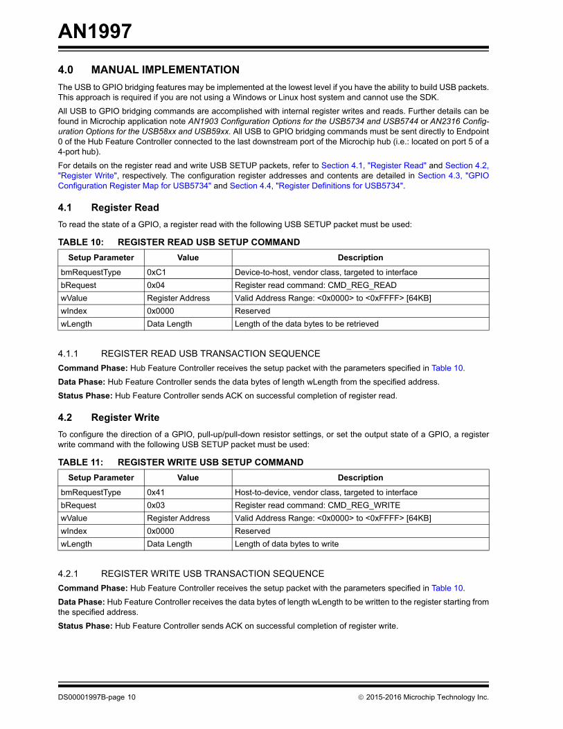
4.0 MANUAL IMPLEMENTATION
The USB to GPIO bridging features may be implemented at the lowest level if you have the ability to build USB packets. This approach is required if you are not using a Windows or Linux host system and cannot use the SDK.
All USB to GPIO bridging commands are accomplished with internal register writes and reads. Further details can be found in Microchip application note AN1903 Configuration Options for the USB5734 and USB5744 or AN2316 Config-uration Options for the USB58xx and USB59xx. All USB to GPIO bridging commands must be sent directly to Endpoint 0 of the Hub Feature Controller connected to the last downstream port of the Microchip hub (i.e.: located on port 5 of a 4-port hub).
For details on the register read and write USB SETUP packets, refer to Section 4.1, "Register Read" and Section 4.2, "Register Write", respectively. The configuration register addresses and contents are detailed in Section 4.3, "GPIO Configuration Register Map for USB5734" and Section 4.4, "Register Definitions for USB5734".
4.1 Register Read
To read the state of a GPIO, a register read with the following USB SETUP packet must be used:
TABLE 10: REGISTER READ USB SETUP COMMAND
Setup Parameter Value Description
bmRequestType 0xC1 Device-to-host, vendor class, targeted to interface
bRequest 0x04 Register read command: CMD_REG_READ
wValue Register Address Valid Address Range: <0x0000> to <0xFFFF> [64KB]
wIndex 0x0000 Reserved
wLength Data Length Length of the data bytes to be retrieved
4.1.1 REGISTER READ USB TRANSACTION SEQUENCE
Command Phase: Hub Feature Controller receives the setup packet with the parameters specified in Table 10.
Data Phase: Hub Feature Controller sends the data bytes of length wLength from the specified address.
Status Phase: Hub Feature Controller sends ACK on successful completion of register read.
4.2 Register Write
To configure the direction of a GPIO, pull-up/pull-down resistor settings, or set the output state of a GPIO, a register write command with the following USB SETUP packet must be used:
TABLE 11: REGISTER WRITE USB SETUP COMMAND
Setup Parameter Value Description
bmRequestType 0x41 Host-to-device, vendor class, targeted to interface
bRequest 0x03 Register read command: CMD_REG_WRITE
wValue Register Address Valid Address Range: <0x0000> to <0xFFFF> [64KB]
wIndex 0x0000 Reserved
wLength Data Length Length of data bytes to write
4.2.1 REGISTER WRITE USB TRANSACTION SEQUENCE
Command Phase: Hub Feature Controller receives the setup packet with the parameters specified in Table 10.
Data Phase: Hub Feature Controller receives the data bytes of length wLength to be written to the register starting from the specified address.
Status Phase: Hub Feature Controller sends ACK on successful completion of register write.
DS00001997B-page 10 2015-2016 Microchip Technology Inc.
AN1997
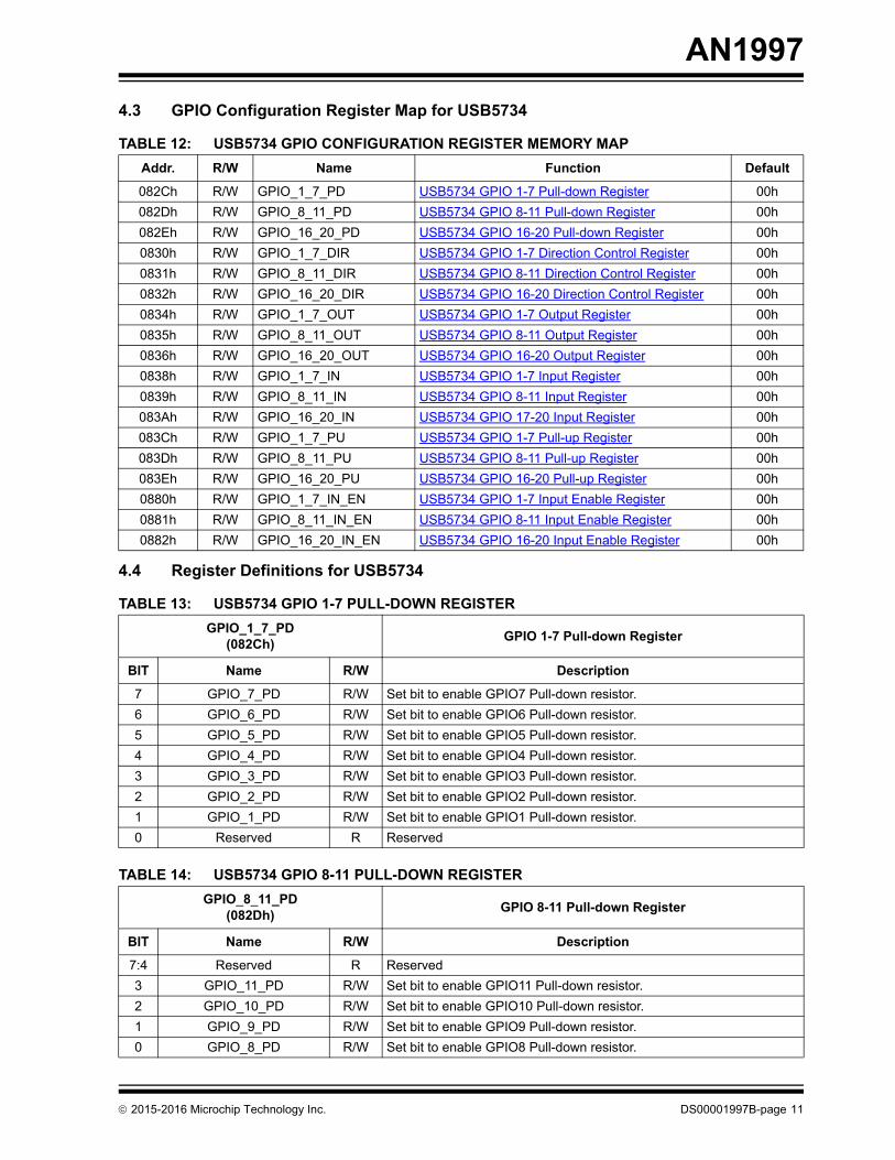
4.3 GPIO Configuration Register Map for USB5734
TABLE 12: USB5734 GPIO CONFIGURATION REGISTER MEMORY MAP
Addr. R/W Name Function Default
082Ch R/W GPIO_1_7_PD USB5734 GPIO 1-7 Pull-down Register 00h
082Dh R/W GPIO_8_11_PD USB5734 GPIO 8-11 Pull-down Register 00h
082Eh R/W GPIO_16_20_PD USB5734 GPIO 16-20 Pull-down Register 00h
0830h R/W GPIO_1_7_DIR USB5734 GPIO 1-7 Direction Control Register 00h
0831h R/W GPIO_8_11_DIR USB5734 GPIO 8-11 Direction Control Register 00h
0832h R/W GPIO_16_20_DIR USB5734 GPIO 16-20 Direction Control Register 00h
0834h R/W GPIO_1_7_OUT USB5734 GPIO 1-7 Output Register 00h
0835h R/W GPIO_8_11_OUT USB5734 GPIO 8-11 Output Register 00h
0836h R/W GPIO_16_20_OUT USB5734 GPIO 16-20 Output Register 00h
0838h R/W GPIO_1_7_IN USB5734 GPIO 1-7 Input Register 00h
0839h R/W GPIO_8_11_IN USB5734 GPIO 8-11 Input Register 00h
083Ah R/W GPIO_16_20_IN USB5734 GPIO 17-20 Input Register 00h
083Ch R/W GPIO_1_7_PU USB5734 GPIO 1-7 Pull-up Register 00h
083Dh R/W GPIO_8_11_PU USB5734 GPIO 8-11 Pull-up Register 00h
083Eh R/W GPIO_16_20_PU USB5734 GPIO 16-20 Pull-up Register 00h
0880h R/W GPIO_1_7_IN_EN USB5734 GPIO 1-7 Input Enable Register 00h
0881h R/W GPIO_8_11_IN_EN USB5734 GPIO 8-11 Input Enable Register 00h
0882h R/W GPIO_16_20_IN_EN USB5734 GPIO 16-20 Input Enable Register 00h
4.4 Register Definitions for USB5734
TABLE 13: USB5734 GPIO 1-7 PULL-DOWN REGISTER
GPIO_1_7_PD(082Ch)
GPIO 1-7 Pull-down Register
BIT Name R/W Description
7 GPIO_7_PD R/W Set bit to enable GPIO7 Pull-down resistor.
6 GPIO_6_PD R/W Set bit to enable GPIO6 Pull-down resistor.
5 GPIO_5_PD R/W Set bit to enable GPIO5 Pull-down resistor.
4 GPIO_4_PD R/W Set bit to enable GPIO4 Pull-down resistor.
3 GPIO_3_PD R/W Set bit to enable GPIO3 Pull-down resistor.
2 GPIO_2_PD R/W Set bit to enable GPIO2 Pull-down resistor.
1 GPIO_1_PD R/W Set bit to enable GPIO1 Pull-down resistor.
0 Reserved R Reserved
TABLE 14: USB5734 GPIO 8-11 PULL-DOWN REGISTER
GPIO_8_11_PD(082Dh)
GPIO 8-11 Pull-down Register
BIT Name R/W Description
7:4 Reserved R Reserved
3 GPIO_11_PD R/W Set bit to enable GPIO11 Pull-down resistor.
2 GPIO_10_PD R/W Set bit to enable GPIO10 Pull-down resistor.
1 GPIO_9_PD R/W Set bit to enable GPIO9 Pull-down resistor.
0 GPIO_8_PD R/W Set bit to enable GPIO8 Pull-down resistor.
2015-2016 Microchip Technology Inc. DS00001997B-page 11
AN1997
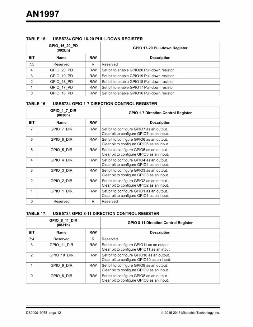
TABLE 15: USB5734 GPIO 16-20 PULL-DOWN REGISTER
GPIO_16_20_PD(082Eh)
GPIO 17-20 Pull-down Register
BIT Name R/W Description
7:5 Reserved R Reserved
4 GPIO_20_PD R/W Set bit to enable GPIO20 Pull-down resistor.
3 GPIO_19_PD R/W Set bit to enable GPIO19 Pull-down resistor.
2 GPIO_18_PD R/W Set bit to enable GPIO18 Pull-down resistor.
1 GPIO_17_PD R/W Set bit to enable GPIO17 Pull-down resistor.
0 GPIO_16_PD R/W Set bit to enable GPIO16 Pull-down resistor.
TABLE 16: USB5734 GPIO 1-7 DIRECTION CONTROL REGISTER
GPIO_1_7_DIR(0830h)
GPIO 1-7 Direction Control Register
BIT Name R/W Description
7 GPIO_7_DIR R/W Set bit to configure GPIO7 as an output.Clear bit to configure GPIO7 as an input.
6 GPIO_6_DIR R/W Set bit to configure GPIO6 as an output.Clear bit to configure GPIO6 as an input.
5 GPIO_5_DIR R/W Set bit to configure GPIO5 as an output.Clear bit to configure GPIO5 as an input.
4 GPIO_4_DIR R/W Set bit to configure GPIO4 as an output.Clear bit to configure GPIO4 as an input.
3 GPIO_3_DIR R/W Set bit to configure GPIO3 as an output.Clear bit to configure GPIO3 as an input.
2 GPIO_2_DIR R/W Set bit to configure GPIO2 as an output.Clear bit to configure GPIO2 as an input.
1 GPIO_1_DIR R/W Set bit to configure GPIO1 as an output.Clear bit to configure GPIO1 as an input.
0 Reserved R Reserved
TABLE 17: USB5734 GPIO 8-11 DIRECTION CONTROL REGISTER
GPIO_8_11_DIR(0831h)
GPIO 8-11 Direction Control Register
BIT Name R/W Description
7:4 Reserved R Reserved
3 GPIO_11_DIR R/W Set bit to configure GPIO11 as an output.Clear bit to configure GPIO11 as an input.
2 GPIO_10_DIR R/W Set bit to configure GPIO10 as an output.Clear bit to configure GPIO10 as an input.
1 GPIO_9_DIR R/W Set bit to configure GPIO9 as an output.Clear bit to configure GPIO9 as an input.
0 GPIO_8_DIR R/W Set bit to configure GPIO8 as an output.Clear bit to configure GPIO8 as an input.
DS00001997B-page 12 2015-2016 Microchip Technology Inc.
AN1997
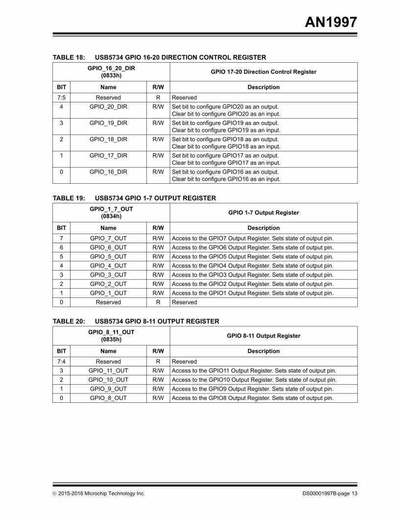
TABLE 18: USB5734 GPIO 16-20 DIRECTION CONTROL REGISTER
GPIO_16_20_DIR(0833h)
GPIO 17-20 Direction Control Register
BIT Name R/W Description
7:5 Reserved R Reserved
4 GPIO_20_DIR R/W Set bit to configure GPIO20 as an output.Clear bit to configure GPIO20 as an input.
3 GPIO_19_DIR R/W Set bit to configure GPIO19 as an output.Clear bit to configure GPIO19 as an input.
2 GPIO_18_DIR R/W Set bit to configure GPIO18 as an output.Clear bit to configure GPIO18 as an input.
1 GPIO_17_DIR R/W Set bit to configure GPIO17 as an output.Clear bit to configure GPIO17 as an input.
0 GPIO_16_DIR R/W Set bit to configure GPIO16 as an output.Clear bit to configure GPIO16 as an input.
TABLE 19: USB5734 GPIO 1-7 OUTPUT REGISTER
GPIO_1_7_OUT(0834h)
GPIO 1-7 Output Register
BIT Name R/W Description
7 GPIO_7_OUT R/W Access to the GPIO7 Output Register. Sets state of output pin.
6 GPIO_6_OUT R/W Access to the GPIO6 Output Register. Sets state of output pin.
5 GPIO_5_OUT R/W Access to the GPIO5 Output Register. Sets state of output pin.
4 GPIO_4_OUT R/W Access to the GPIO4 Output Register. Sets state of output pin.
3 GPIO_3_OUT R/W Access to the GPIO3 Output Register. Sets state of output pin.
2 GPIO_2_OUT R/W Access to the GPIO2 Output Register. Sets state of output pin.
1 GPIO_1_OUT R/W Access to the GPIO1 Output Register. Sets state of output pin.
0 Reserved R Reserved
TABLE 20: USB5734 GPIO 8-11 OUTPUT REGISTER
GPIO_8_11_OUT(0835h)
GPIO 8-11 Output Register
BIT Name R/W Description
7:4 Reserved R Reserved
3 GPIO_11_OUT R/W Access to the GPIO11 Output Register. Sets state of output pin.
2 GPIO_10_OUT R/W Access to the GPIO10 Output Register. Sets state of output pin.
1 GPIO_9_OUT R/W Access to the GPIO9 Output Register. Sets state of output pin.
0 GPIO_8_OUT R/W Access to the GPIO8 Output Register. Sets state of output pin.
2015-2016 Microchip Technology Inc. DS00001997B-page 13
AN1997
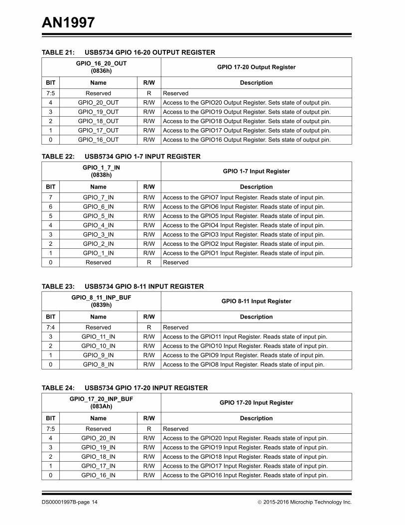
TABLE 21: USB5734 GPIO 16-20 OUTPUT REGISTER
GPIO_16_20_OUT(0836h)
GPIO 17-20 Output Register
BIT Name R/W Description
7:5 Reserved R Reserved
4 GPIO_20_OUT R/W Access to the GPIO20 Output Register. Sets state of output pin.
3 GPIO_19_OUT R/W Access to the GPIO19 Output Register. Sets state of output pin.
2 GPIO_18_OUT R/W Access to the GPIO18 Output Register. Sets state of output pin.
1 GPIO_17_OUT R/W Access to the GPIO17 Output Register. Sets state of output pin.
0 GPIO_16_OUT R/W Access to the GPIO16 Output Register. Sets state of output pin.
TABLE 22: USB5734 GPIO 1-7 INPUT REGISTER
GPIO_1_7_IN(0838h)
GPIO 1-7 Input Register
BIT Name R/W Description
7 GPIO_7_IN R/W Access to the GPIO7 Input Register. Reads state of input pin.
6 GPIO_6_IN R/W Access to the GPIO6 Input Register. Reads state of input pin.
5 GPIO_5_IN R/W Access to the GPIO5 Input Register. Reads state of input pin.
4 GPIO_4_IN R/W Access to the GPIO4 Input Register. Reads state of input pin.
3 GPIO_3_IN R/W Access to the GPIO3 Input Register. Reads state of input pin.
2 GPIO_2_IN R/W Access to the GPIO2 Input Register. Reads state of input pin.
1 GPIO_1_IN R/W Access to the GPIO1 Input Register. Reads state of input pin.
0 Reserved R Reserved
TABLE 23: USB5734 GPIO 8-11 INPUT REGISTER
GPIO_8_11_INP_BUF(0839h)
GPIO 8-11 Input Register
BIT Name R/W Description
7:4 Reserved R Reserved
3 GPIO_11_IN R/W Access to the GPIO11 Input Register. Reads state of input pin.
2 GPIO_10_IN R/W Access to the GPIO10 Input Register. Reads state of input pin.
1 GPIO_9_IN R/W Access to the GPIO9 Input Register. Reads state of input pin.
0 GPIO_8_IN R/W Access to the GPIO8 Input Register. Reads state of input pin.
TABLE 24: USB5734 GPIO 17-20 INPUT REGISTER
GPIO_17_20_INP_BUF(083Ah)
GPIO 17-20 Input Register
BIT Name R/W Description
7:5 Reserved R Reserved
4 GPIO_20_IN R/W Access to the GPIO20 Input Register. Reads state of input pin.
3 GPIO_19_IN R/W Access to the GPIO19 Input Register. Reads state of input pin.
2 GPIO_18_IN R/W Access to the GPIO18 Input Register. Reads state of input pin.
1 GPIO_17_IN R/W Access to the GPIO17 Input Register. Reads state of input pin.
0 GPIO_16_IN R/W Access to the GPIO16 Input Register. Reads state of input pin.
DS00001997B-page 14 2015-2016 Microchip Technology Inc.
AN1997
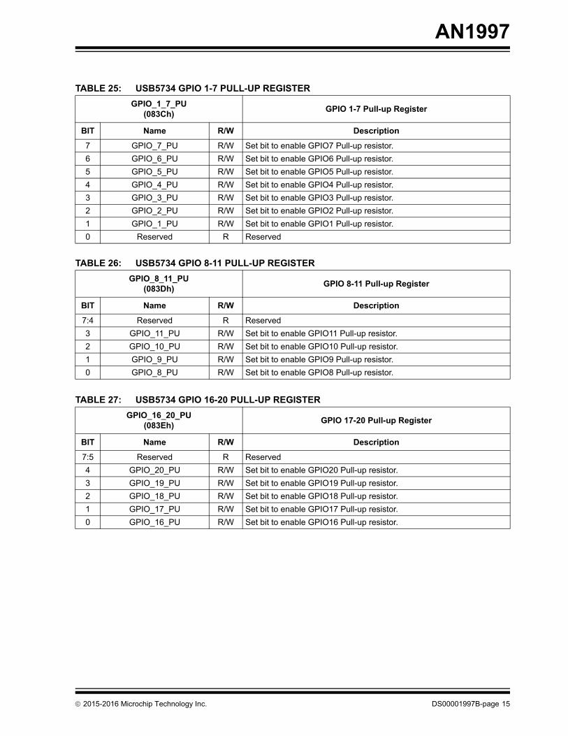
TABLE 25: USB5734 GPIO 1-7 PULL-UP REGISTER
GPIO_1_7_PU(083Ch)
GPIO 1-7 Pull-up Register
BIT Name R/W Description
7 GPIO_7_PU R/W Set bit to enable GPIO7 Pull-up resistor.
6 GPIO_6_PU R/W Set bit to enable GPIO6 Pull-up resistor.
5 GPIO_5_PU R/W Set bit to enable GPIO5 Pull-up resistor.
4 GPIO_4_PU R/W Set bit to enable GPIO4 Pull-up resistor.
3 GPIO_3_PU R/W Set bit to enable GPIO3 Pull-up resistor.
2 GPIO_2_PU R/W Set bit to enable GPIO2 Pull-up resistor.
1 GPIO_1_PU R/W Set bit to enable GPIO1 Pull-up resistor.
0 Reserved R Reserved
TABLE 26: USB5734 GPIO 8-11 PULL-UP REGISTER
GPIO_8_11_PU(083Dh)
GPIO 8-11 Pull-up Register
BIT Name R/W Description
7:4 Reserved R Reserved
3 GPIO_11_PU R/W Set bit to enable GPIO11 Pull-up resistor.
2 GPIO_10_PU R/W Set bit to enable GPIO10 Pull-up resistor.
1 GPIO_9_PU R/W Set bit to enable GPIO9 Pull-up resistor.
0 GPIO_8_PU R/W Set bit to enable GPIO8 Pull-up resistor.
TABLE 27: USB5734 GPIO 16-20 PULL-UP REGISTER
GPIO_16_20_PU(083Eh)
GPIO 17-20 Pull-up Register
BIT Name R/W Description
7:5 Reserved R Reserved
4 GPIO_20_PU R/W Set bit to enable GPIO20 Pull-up resistor.
3 GPIO_19_PU R/W Set bit to enable GPIO19 Pull-up resistor.
2 GPIO_18_PU R/W Set bit to enable GPIO18 Pull-up resistor.
1 GPIO_17_PU R/W Set bit to enable GPIO17 Pull-up resistor.
0 GPIO_16_PU R/W Set bit to enable GPIO16 Pull-up resistor.
2015-2016 Microchip Technology Inc. DS00001997B-page 15
AN1997
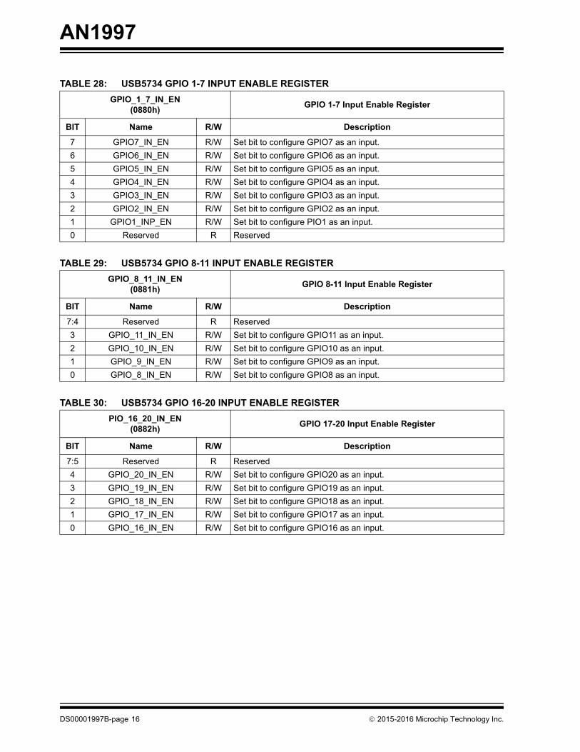
TABLE 28: USB5734 GPIO 1-7 INPUT ENABLE REGISTER
GPIO_1_7_IN_EN(0880h)
GPIO 1-7 Input Enable Register
BIT Name R/W Description
7 GPIO7_IN_EN R/W Set bit to configure GPIO7 as an input.
6 GPIO6_IN_EN R/W Set bit to configure GPIO6 as an input.
5 GPIO5_IN_EN R/W Set bit to configure GPIO5 as an input.
4 GPIO4_IN_EN R/W Set bit to configure GPIO4 as an input.
3 GPIO3_IN_EN R/W Set bit to configure GPIO3 as an input.
2 GPIO2_IN_EN R/W Set bit to configure GPIO2 as an input.
1 GPIO1_INP_EN R/W Set bit to configure PIO1 as an input.
0 Reserved R Reserved
TABLE 29: USB5734 GPIO 8-11 INPUT ENABLE REGISTER
GPIO_8_11_IN_EN(0881h)
GPIO 8-11 Input Enable Register
BIT Name R/W Description
7:4 Reserved R Reserved
3 GPIO_11_IN_EN R/W Set bit to configure GPIO11 as an input.
2 GPIO_10_IN_EN R/W Set bit to configure GPIO10 as an input.
1 GPIO_9_IN_EN R/W Set bit to configure GPIO9 as an input.
0 GPIO_8_IN_EN R/W Set bit to configure GPIO8 as an input.
TABLE 30: USB5734 GPIO 16-20 INPUT ENABLE REGISTER
PIO_16_20_IN_EN(0882h)
GPIO 17-20 Input Enable Register
BIT Name R/W Description
7:5 Reserved R Reserved
4 GPIO_20_IN_EN R/W Set bit to configure GPIO20 as an input.
3 GPIO_19_IN_EN R/W Set bit to configure GPIO19 as an input.
2 GPIO_18_IN_EN R/W Set bit to configure GPIO18 as an input.
1 GPIO_17_IN_EN R/W Set bit to configure GPIO17 as an input.
0 GPIO_16_IN_EN R/W Set bit to configure GPIO16 as an input.
DS00001997B-page 16 2015-2016 Microchip Technology Inc.
AN1997
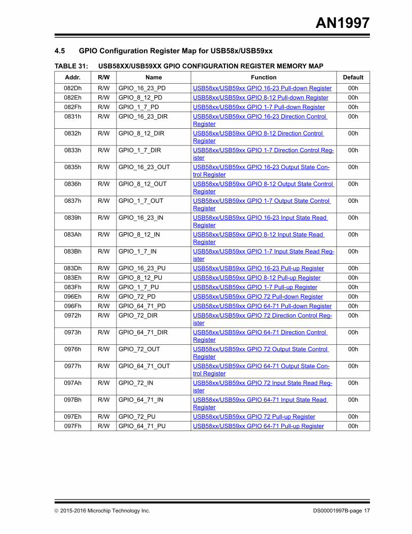
4.5 GPIO Configuration Register Map for USB58x/USB59xx
TABLE 31: USB58XX/USB59XX GPIO CONFIGURATION REGISTER MEMORY MAP
Addr. R/W Name Function Default
082Dh R/W GPIO_16_23_PD USB58xx/USB59xx GPIO 16-23 Pull-down Register 00h
082Eh R/W GPIO_8_12_PD USB58xx/USB59xx GPIO 8-12 Pull-down Register 00h
082Fh R/W GPIO_1_7_PD USB58xx/USB59xx GPIO 1-7 Pull-down Register 00h
0831h R/W GPIO_16_23_DIR USB58xx/USB59xx GPIO 16-23 Direction Control Register
00h
0832h R/W GPIO_8_12_DIR USB58xx/USB59xx GPIO 8-12 Direction Control Register
00h
0833h R/W GPIO_1_7_DIR USB58xx/USB59xx GPIO 1-7 Direction Control Reg-ister
00h
0835h R/W GPIO_16_23_OUT USB58xx/USB59xx GPIO 16-23 Output State Con-trol Register
00h
0836h R/W GPIO_8_12_OUT USB58xx/USB59xx GPIO 8-12 Output State Control Register
00h
0837h R/W GPIO_1_7_OUT USB58xx/USB59xx GPIO 1-7 Output State Control Register
00h
0839h R/W GPIO_16_23_IN USB58xx/USB59xx GPIO 16-23 Input State Read Register
00h
083Ah R/W GPIO_8_12_IN USB58xx/USB59xx GPIO 8-12 Input State Read Register
00h
083Bh R/W GPIO_1_7_IN USB58xx/USB59xx GPIO 1-7 Input State Read Reg-ister
00h
083Dh R/W GPIO_16_23_PU USB58xx/USB59xx GPIO 16-23 Pull-up Register 00h
083Eh R/W GPIO_8_12_PU USB58xx/USB59xx GPIO 8-12 Pull-up Register 00h
083Fh R/W GPIO_1_7_PU USB58xx/USB59xx GPIO 1-7 Pull-up Register 00h
096Eh R/W GPIO_72_PD USB58xx/USB59xx GPIO 72 Pull-down Register 00h
096Fh R/W GPIO_64_71_PD USB58xx/USB59xx GPIO 64-71 Pull-down Register 00h
0972h R/W GPIO_72_DIR USB58xx/USB59xx GPIO 72 Direction Control Reg-ister
00h
0973h R/W GPIO_64_71_DIR USB58xx/USB59xx GPIO 64-71 Direction Control Register
00h
0976h R/W GPIO_72_OUT USB58xx/USB59xx GPIO 72 Output State Control Register
00h
0977h R/W GPIO_64_71_OUT USB58xx/USB59xx GPIO 64-71 Output State Con-trol Register
00h
097Ah R/W GPIO_72_IN USB58xx/USB59xx GPIO 72 Input State Read Reg-ister
00h
097Bh R/W GPIO_64_71_IN USB58xx/USB59xx GPIO 64-71 Input State Read Register
00h
097Eh R/W GPIO_72_PU USB58xx/USB59xx GPIO 72 Pull-up Register 00h
097Fh R/W GPIO_64_71_PU USB58xx/USB59xx GPIO 64-71 Pull-up Register 00h
2015-2016 Microchip Technology Inc. DS00001997B-page 17
AN1997
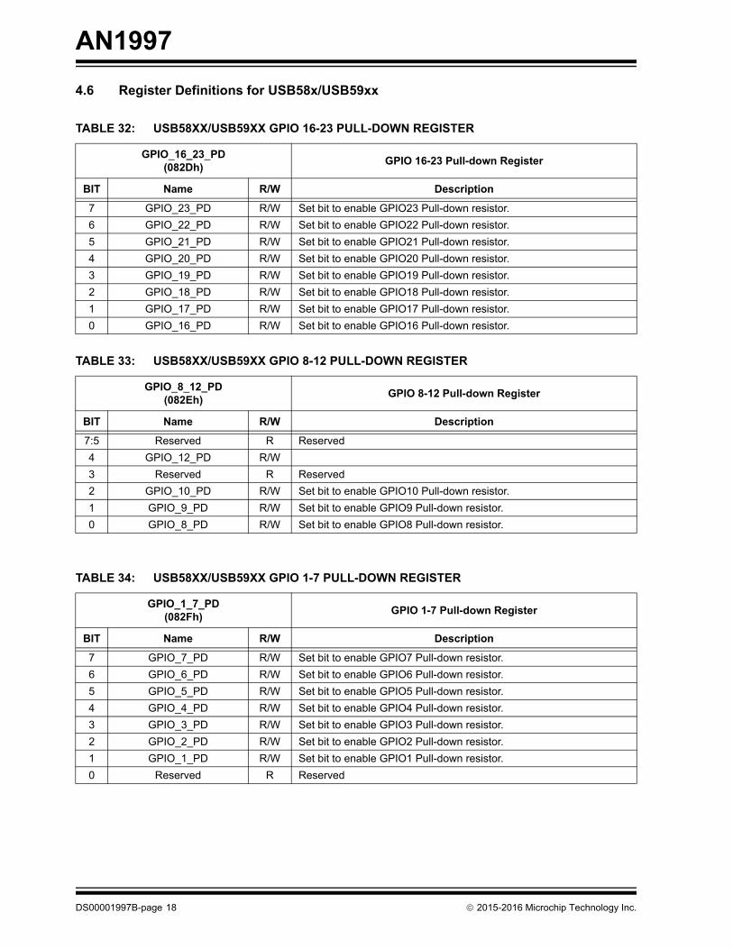
4.6 Register Definitions for USB58x/USB59xx
TABLE 32: USB58XX/USB59XX GPIO 16-23 PULL-DOWN REGISTER
GPIO_16_23_PD(082Dh)
GPIO 16-23 Pull-down Register
BIT Name R/W Description
7 GPIO_23_PD R/W Set bit to enable GPIO23 Pull-down resistor.
6 GPIO_22_PD R/W Set bit to enable GPIO22 Pull-down resistor.
5 GPIO_21_PD R/W Set bit to enable GPIO21 Pull-down resistor.
4 GPIO_20_PD R/W Set bit to enable GPIO20 Pull-down resistor.
3 GPIO_19_PD R/W Set bit to enable GPIO19 Pull-down resistor.
2 GPIO_18_PD R/W Set bit to enable GPIO18 Pull-down resistor.
1 GPIO_17_PD R/W Set bit to enable GPIO17 Pull-down resistor.
0 GPIO_16_PD R/W Set bit to enable GPIO16 Pull-down resistor.
TABLE 33: USB58XX/USB59XX GPIO 8-12 PULL-DOWN REGISTER
GPIO_8_12_PD(082Eh)
GPIO 8-12 Pull-down Register
BIT Name R/W Description
7:5 Reserved R Reserved
4 GPIO_12_PD R/W
3 Reserved R Reserved
2 GPIO_10_PD R/W Set bit to enable GPIO10 Pull-down resistor.
1 GPIO_9_PD R/W Set bit to enable GPIO9 Pull-down resistor.
0 GPIO_8_PD R/W Set bit to enable GPIO8 Pull-down resistor.
TABLE 34: USB58XX/USB59XX GPIO 1-7 PULL-DOWN REGISTER
GPIO_1_7_PD(082Fh)
GPIO 1-7 Pull-down Register
BIT Name R/W Description
7 GPIO_7_PD R/W Set bit to enable GPIO7 Pull-down resistor.
6 GPIO_6_PD R/W Set bit to enable GPIO6 Pull-down resistor.
5 GPIO_5_PD R/W Set bit to enable GPIO5 Pull-down resistor.
4 GPIO_4_PD R/W Set bit to enable GPIO4 Pull-down resistor.
3 GPIO_3_PD R/W Set bit to enable GPIO3 Pull-down resistor.
2 GPIO_2_PD R/W Set bit to enable GPIO2 Pull-down resistor.
1 GPIO_1_PD R/W Set bit to enable GPIO1 Pull-down resistor.
0 Reserved R Reserved
DS00001997B-page 18 2015-2016 Microchip Technology Inc.
AN1997
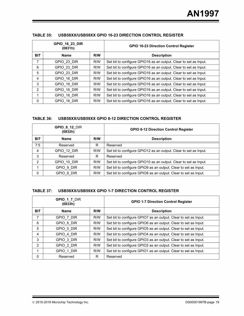
TABLE 35: USB58XX/USB59XX GPIO 16-23 DIRECTION CONTROL REGISTER
GPIO_16_23_DIR(0831h)
GPIO 16-23 Direction Control Register
BIT Name R/W Description
7 GPIO_23_DIR R/W Set bit to configure GPIO16 as an output. Clear to set as Input.
6 GPIO_23_DIR R/W Set bit to configure GPIO16 as an output. Clear to set as Input.
5 GPIO_23_DIR R/W Set bit to configure GPIO16 as an output. Clear to set as Input.
4 GPIO_16_DIR R/W Set bit to configure GPIO16 as an output. Clear to set as Input.
3 GPIO_16_DIR R/W Set bit to configure GPIO16 as an output. Clear to set as Input.
2 GPIO_16_DIR R/W Set bit to configure GPIO16 as an output. Clear to set as Input.
1 GPIO_16_DIR R/W Set bit to configure GPIO16 as an output. Clear to set as Input.
0 GPIO_16_DIR R/W Set bit to configure GPIO16 as an output. Clear to set as Input.
TABLE 36: USB58XX/USB59XX GPIO 8-12 DIRECTION CONTROL REGISTER
GPIO_8_12_DIR(0832h)
GPIO 8-12 Direction Control Register
BIT Name R/W Description
7:5 Reserved R Reserved
4 GPIO_12_DIR R/W Set bit to configure GPIO12 as an output. Clear to set as Input.
3 Reserved R Reserved
2 GPIO_10_DIR R/W Set bit to configure GPIO10 as an output. Clear to set as Input.
1 GPIO_9_DIR R/W Set bit to configure GPIO9 as an output. Clear to set as Input.
0 GPIO_8_DIR R/W Set bit to configure GPIO8 as an output. Clear to set as Input.
TABLE 37: USB58XX/USB59XX GPIO 1-7 DIRECTION CONTROL REGISTER
GPIO_1_7_DIR(0833h)
GPIO 1-7 Direction Control Register
BIT Name R/W Description
7 GPIO_7_DIR R/W Set bit to configure GPIO7 as an output. Clear to set as Input.
6 GPIO_6_DIR R/W Set bit to configure GPIO6 as an output. Clear to set as Input.
5 GPIO_5_DIR R/W Set bit to configure GPIO5 as an output. Clear to set as Input.
4 GPIO_4_DIR R/W Set bit to configure GPIO4 as an output. Clear to set as Input.
3 GPIO_3_DIR R/W Set bit to configure GPIO3 as an output. Clear to set as Input.
2 GPIO_2_DIR R/W Set bit to configure GPIO2 as an output. Clear to set as Input.
1 GPIO_1_DIR R/W Set bit to configure GPIO1 as an output. Clear to set as Input.
0 Reserved R Reserved
2015-2016 Microchip Technology Inc. DS00001997B-page 19
AN1997
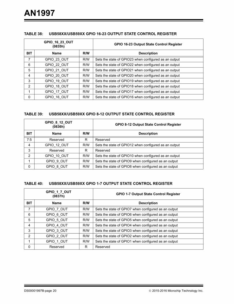
TABLE 38: USB58XX/USB59XX GPIO 16-23 OUTPUT STATE CONTROL REGISTER
GPIO_16_23_OUT(0835h)
GPIO 16-23 Output State Control Register
BIT Name R/W Description
7 GPIO_23_OUT R/W Sets the state of GPIO23 when configured as an output
6 GPIO_22_OUT R/W Sets the state of GPIO22 when configured as an output
5 GPIO_21_OUT R/W Sets the state of GPIO21 when configured as an output
4 GPIO_20_OUT R/W Sets the state of GPIO20 when configured as an output
3 GPIO_19_OUT R/W Sets the state of GPIO19 when configured as an output
2 GPIO_18_OUT R/W Sets the state of GPIO18 when configured as an output
1 GPIO_17_OUT R/W Sets the state of GPIO17 when configured as an output
0 GPIO_16_OUT R/W Sets the state of GPIO16 when configured as an output
TABLE 39: USB58XX/USB59XX GPIO 8-12 OUTPUT STATE CONTROL REGISTER
GPIO_8_12_OUT(0836h)
GPIO 8-12 Output State Control Register
BIT Name R/W Description
7:5 Reserved R Reserved
4 GPIO_12_OUT R/W Sets the state of GPIO12 when configured as an output
3 Reserved R Reserved
2 GPIO_10_OUT R/W Sets the state of GPIO10 when configured as an output
1 GPIO_9_OUT R/W Sets the state of GPIO9 when configured as an output
0 GPIO_8_OUT R/W Sets the state of GPIO8 when configured as an output
TABLE 40: USB58XX/USB59XX GPIO 1-7 OUTPUT STATE CONTROL REGISTER
GPIO_1_7_OUT(0837h)
GPIO 1-7 Output State Control Register
BIT Name R/W Description
7 GPIO_7_OUT R/W Sets the state of GPIO7 when configured as an output
6 GPIO_6_OUT R/W Sets the state of GPIO6 when configured as an output
5 GPIO_5_OUT R/W Sets the state of GPIO5 when configured as an output
4 GPIO_4_OUT R/W Sets the state of GPIO4 when configured as an output
3 GPIO_3_OUT R/W Sets the state of GPIO3 when configured as an output
2 GPIO_2_OUT R/W Sets the state of GPIO2 when configured as an output
1 GPIO_1_OUT R/W Sets the state of GPIO1 when configured as an output
0 Reserved R Reserved
DS00001997B-page 20 2015-2016 Microchip Technology Inc.
AN1997
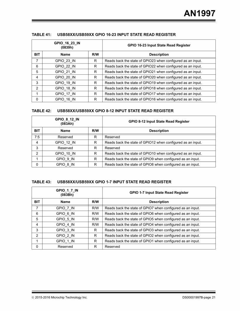
TABLE 41: USB58XX/USB59XX GPIO 16-23 INPUT STATE READ REGISTER
GPIO_16_23_IN(0839h)
GPIO 16-23 Input State Read Register
BIT Name R/W Description
7 GPIO_23_IN R Reads back the state of GPIO23 when configured as an input.
6 GPIO_22_IN R Reads back the state of GPIO22 when configured as an input.
5 GPIO_21_IN R Reads back the state of GPIO21 when configured as an input.
4 GPIO_20_IN R Reads back the state of GPIO20 when configured as an input.
3 GPIO_19_IN R Reads back the state of GPIO19 when configured as an input.
2 GPIO_18_IN R Reads back the state of GPIO18 when configured as an input.
1 GPIO_17_IN R Reads back the state of GPIO17 when configured as an input.
0 GPIO_16_IN R Reads back the state of GPIO16 when configured as an input.
TABLE 42: USB58XX/USB59XX GPIO 8-12 INPUT STATE READ REGISTER
GPIO_8_12_IN(083Ah)
GPIO 8-12 Input State Read Register
BIT Name R/W Description
7:5 Reserved R Reserved
4 GPIO_12_IN R Reads back the state of GPIO12 when configured as an input.
3 Reserved R Reserved
2 GPIO_10_IN R Reads back the state of GPIO10 when configured as an input.
1 GPIO_9_IN R Reads back the state of GPIO9 when configured as an input.
0 GPIO_8_IN R Reads back the state of GPIO8 when configured as an input.
TABLE 43: USB58XX/USB59XX GPIO 1-7 INPUT STATE READ REGISTER
GPIO_1_7_IN(083Bh)
GPIO 1-7 Input State Read Register
BIT Name R/W Description
7 GPIO_7_IN R/W Reads back the state of GPIO7 when configured as an input.
6 GPIO_6_IN R/W Reads back the state of GPIO6 when configured as an input.
5 GPIO_5_IN R/W Reads back the state of GPIO5 when configured as an input.
4 GPIO_4_IN R/W Reads back the state of GPIO4 when configured as an input.
3 GPIO_3_IN R Reads back the state of GPIO3 when configured as an input.
2 GPIO_2_IN R Reads back the state of GPIO2 when configured as an input.
1 GPIO_1_IN R Reads back the state of GPIO1 when configured as an input.
0 Reserved R Reserved
2015-2016 Microchip Technology Inc. DS00001997B-page 21
AN1997
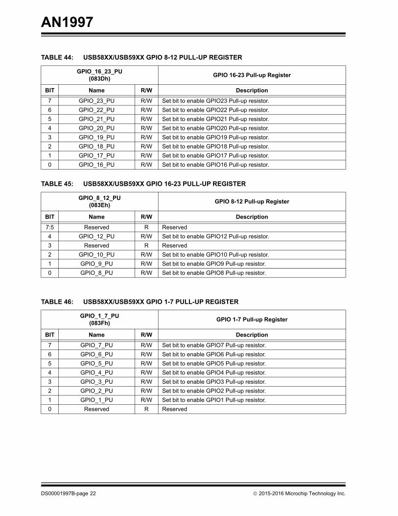
TABLE 44: USB58XX/USB59XX GPIO 8-12 PULL-UP REGISTER
GPIO_16_23_PU(083Dh)
GPIO 16-23 Pull-up Register
BIT Name R/W Description
7 GPIO_23_PU R/W Set bit to enable GPIO23 Pull-up resistor.
6 GPIO_22_PU R/W Set bit to enable GPIO22 Pull-up resistor.
5 GPIO_21_PU R/W Set bit to enable GPIO21 Pull-up resistor.
4 GPIO_20_PU R/W Set bit to enable GPIO20 Pull-up resistor.
3 GPIO_19_PU R/W Set bit to enable GPIO19 Pull-up resistor.
2 GPIO_18_PU R/W Set bit to enable GPIO18 Pull-up resistor.
1 GPIO_17_PU R/W Set bit to enable GPIO17 Pull-up resistor.
0 GPIO_16_PU R/W Set bit to enable GPIO16 Pull-up resistor.
TABLE 45: USB58XX/USB59XX GPIO 16-23 PULL-UP REGISTER
GPIO_8_12_PU(083Eh)
GPIO 8-12 Pull-up Register
BIT Name R/W Description
7:5 Reserved R Reserved
4 GPIO_12_PU R/W Set bit to enable GPIO12 Pull-up resistor.
3 Reserved R Reserved
2 GPIO_10_PU R/W Set bit to enable GPIO10 Pull-up resistor.
1 GPIO_9_PU R/W Set bit to enable GPIO9 Pull-up resistor.
0 GPIO_8_PU R/W Set bit to enable GPIO8 Pull-up resistor.
TABLE 46: USB58XX/USB59XX GPIO 1-7 PULL-UP REGISTER
GPIO_1_7_PU(083Fh)
GPIO 1-7 Pull-up Register
BIT Name R/W Description
7 GPIO_7_PU R/W Set bit to enable GPIO7 Pull-up resistor.
6 GPIO_6_PU R/W Set bit to enable GPIO6 Pull-up resistor.
5 GPIO_5_PU R/W Set bit to enable GPIO5 Pull-up resistor.
4 GPIO_4_PU R/W Set bit to enable GPIO4 Pull-up resistor.
3 GPIO_3_PU R/W Set bit to enable GPIO3 Pull-up resistor.
2 GPIO_2_PU R/W Set bit to enable GPIO2 Pull-up resistor.
1 GPIO_1_PU R/W Set bit to enable GPIO1 Pull-up resistor.
0 Reserved R Reserved
DS00001997B-page 22 2015-2016 Microchip Technology Inc.
AN1997
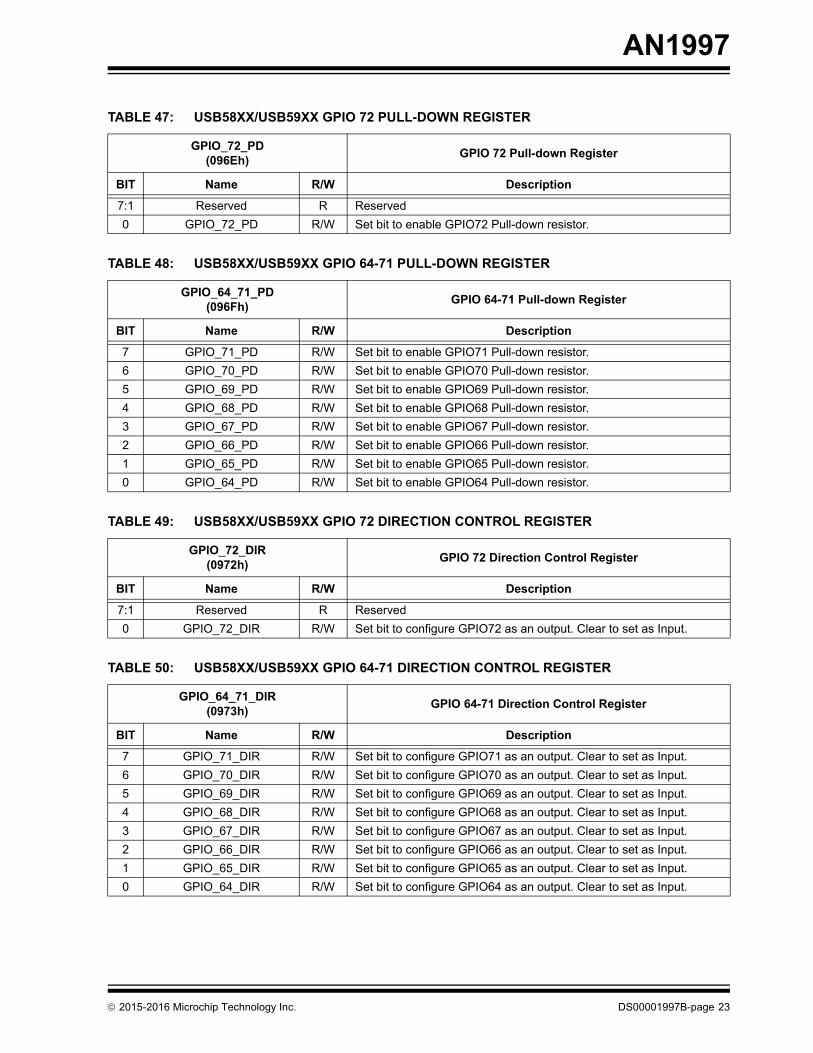
TABLE 47: USB58XX/USB59XX GPIO 72 PULL-DOWN REGISTER
GPIO_72_PD(096Eh)
GPIO 72 Pull-down Register
BIT Name R/W Description
7:1 Reserved R Reserved
0 GPIO_72_PD R/W Set bit to enable GPIO72 Pull-down resistor.
TABLE 48: USB58XX/USB59XX GPIO 64-71 PULL-DOWN REGISTER
GPIO_64_71_PD(096Fh)
GPIO 64-71 Pull-down Register
BIT Name R/W Description
7 GPIO_71_PD R/W Set bit to enable GPIO71 Pull-down resistor.
6 GPIO_70_PD R/W Set bit to enable GPIO70 Pull-down resistor.
5 GPIO_69_PD R/W Set bit to enable GPIO69 Pull-down resistor.
4 GPIO_68_PD R/W Set bit to enable GPIO68 Pull-down resistor.
3 GPIO_67_PD R/W Set bit to enable GPIO67 Pull-down resistor.
2 GPIO_66_PD R/W Set bit to enable GPIO66 Pull-down resistor.
1 GPIO_65_PD R/W Set bit to enable GPIO65 Pull-down resistor.
0 GPIO_64_PD R/W Set bit to enable GPIO64 Pull-down resistor.
TABLE 49: USB58XX/USB59XX GPIO 72 DIRECTION CONTROL REGISTER
GPIO_72_DIR(0972h)
GPIO 72 Direction Control Register
BIT Name R/W Description
7:1 Reserved R Reserved
0 GPIO_72_DIR R/W Set bit to configure GPIO72 as an output. Clear to set as Input.
TABLE 50: USB58XX/USB59XX GPIO 64-71 DIRECTION CONTROL REGISTER
GPIO_64_71_DIR(0973h)
GPIO 64-71 Direction Control Register
BIT Name R/W Description
7 GPIO_71_DIR R/W Set bit to configure GPIO71 as an output. Clear to set as Input.
6 GPIO_70_DIR R/W Set bit to configure GPIO70 as an output. Clear to set as Input.
5 GPIO_69_DIR R/W Set bit to configure GPIO69 as an output. Clear to set as Input.
4 GPIO_68_DIR R/W Set bit to configure GPIO68 as an output. Clear to set as Input.
3 GPIO_67_DIR R/W Set bit to configure GPIO67 as an output. Clear to set as Input.
2 GPIO_66_DIR R/W Set bit to configure GPIO66 as an output. Clear to set as Input.
1 GPIO_65_DIR R/W Set bit to configure GPIO65 as an output. Clear to set as Input.
0 GPIO_64_DIR R/W Set bit to configure GPIO64 as an output. Clear to set as Input.
2015-2016 Microchip Technology Inc. DS00001997B-page 23
AN1997
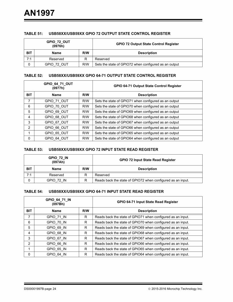
TABLE 51: USB58XX/USB59XX GPIO 72 OUTPUT STATE CONTROL REGISTER
GPIO_72_OUT(0976h)
GPIO 72 Output State Control Register
BIT Name R/W Description
7:1 Reserved R Reserved
0 GPIO_72_OUT R/W Sets the state of GPIO72 when configured as an output
TABLE 52: USB58XX/USB59XX GPIO 64-71 OUTPUT STATE CONTROL REGISTER
GPIO_64_71_OUT(0977h)
GPIO 64-71 Output State Control Register
BIT Name R/W Description
7 GPIO_71_OUT R/W Sets the state of GPIO71 when configured as an output
6 GPIO_70_OUT R/W Sets the state of GPIO70 when configured as an output
5 GPIO_69_OUT R/W Sets the state of GPIO69 when configured as an output
4 GPIO_68_OUT R/W Sets the state of GPIO68 when configured as an output
3 GPIO_67_OUT R/W Sets the state of GPIO67 when configured as an output
2 GPIO_66_OUT R/W Sets the state of GPIO66 when configured as an output
1 GPIO_65_OUT R/W Sets the state of GPIO65 when configured as an output
0 GPIO_64_OUT R/W Sets the state of GPIO64 when configured as an output
TABLE 53: USB58XX/USB59XX GPIO 72 INPUT STATE READ REGISTER
GPIO_72_IN(097Ah)
GPIO 72 Input State Read Register
BIT Name R/W Description
7:1 Reserved R Reserved
0 GPIO_72_IN R Reads back the state of GPIO72 when configured as an input.
TABLE 54: USB58XX/USB59XX GPIO 64-71 INPUT STATE READ REGISTER
GPIO_64_71_IN(097Bh)
GPIO 64-71 Input State Read Register
BIT Name R/W Description
7 GPIO_71_IN R Reads back the state of GPIO71 when configured as an input.
6 GPIO_70_IN R Reads back the state of GPIO70 when configured as an input.
5 GPIO_69_IN R Reads back the state of GPIO69 when configured as an input.
4 GPIO_68_IN R Reads back the state of GPIO68 when configured as an input.
3 GPIO_67_IN R Reads back the state of GPIO67 when configured as an input.
2 GPIO_66_IN R Reads back the state of GPIO66 when configured as an input.
1 GPIO_65_IN R Reads back the state of GPIO65 when configured as an input.
0 GPIO_64_IN R Reads back the state of GPIO64 when configured as an input.
DS00001997B-page 24 2015-2016 Microchip Technology Inc.
AN1997
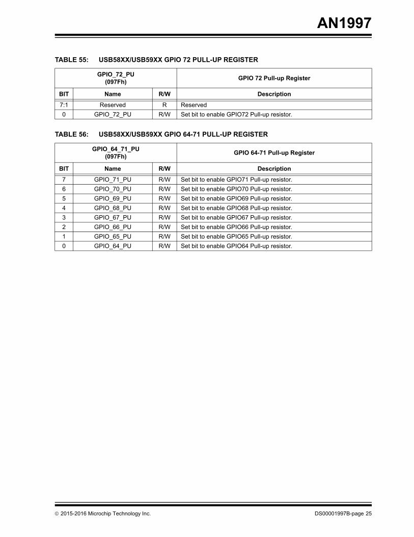
TABLE 55: USB58XX/USB59XX GPIO 72 PULL-UP REGISTER
GPIO_72_PU(097Fh)
GPIO 72 Pull-up Register
BIT Name R/W Description
7:1 Reserved R Reserved
0 GPIO_72_PU R/W Set bit to enable GPIO72 Pull-up resistor.
TABLE 56: USB58XX/USB59XX GPIO 64-71 PULL-UP REGISTER
GPIO_64_71_PU(097Fh)
GPIO 64-71 Pull-up Register
BIT Name R/W Description
7 GPIO_71_PU R/W Set bit to enable GPIO71 Pull-up resistor.
6 GPIO_70_PU R/W Set bit to enable GPIO70 Pull-up resistor.
5 GPIO_69_PU R/W Set bit to enable GPIO69 Pull-up resistor.
4 GPIO_68_PU R/W Set bit to enable GPIO68 Pull-up resistor.
3 GPIO_67_PU R/W Set bit to enable GPIO67 Pull-up resistor.
2 GPIO_66_PU R/W Set bit to enable GPIO66 Pull-up resistor.
1 GPIO_65_PU R/W Set bit to enable GPIO65 Pull-up resistor.
0 GPIO_64_PU R/W Set bit to enable GPIO64 Pull-up resistor.
2015-2016 Microchip Technology Inc. DS00001997B-page 25
AN1997
5.0 EXAMPLES
5.1 Read the Direction State of all GPIOs on USB5734
1. Command Phase (SETUP Transaction): Send the following SETUP Register Read Command to Endpoint 0 of the USB5734 Hub Feature Controller to read the contents of registers 0x830, 0x831, 0x832, and 0x833 which contain the direction control settings for all GPIOs.
TABLE 57: REGISTER READ SETUP COMMAND EXAMPLE
Setup Parameter Value Note
bmRequestType 0xC1 —
bRequest 0x04 —
wValue 0x0830 First register in a series of consecutive registers to read from.
wIndex 0x0000 —
wLength 0x0004 4 consecutive registers are to be read.
FIGURE 5-1: REGISTER READ SETUP TRANSACTION EXAMPLE
2. Data Phase (IN Transaction): Hub Feature Controller sends the data bytes of length wLength starting from the specified address after receiving an IN packet.
FIGURE 1: REGISTER READ IN TRANSACTION EXAMPLE
3. Status Phase (OUT Transaction): Host sends an OUT packet to complete the USB Transfer. Hub Feature Con-troller responds with a zero length data packet.
FIGURE 2: REGISTER READ OUT TRANSACTION EXAMPLE
DS00001997B-page 26 2015-2016 Microchip Technology Inc.
AN1997
5.2 Write Registers to Set GPIO10 as an output on the USB5734
1. Command Phase (SETUP Transaction): Send the following SETUP Register Write Command to Endpoint 0 of the USB5734 Hub Feature Controller to write the contents of registers 0x830, 0x831, 0x832, and 0x833 which contain the direction control settings for all GPIOs. In this example, GPIO10 will be set as an output, all other GPIOS will remain at the default input state.
TABLE 58: REGISTER WRITE SETUP COMMAND EXAMPLE
Setup Parameter Value Note
bmRequestType 0x41 —
bRequest 0x03 —
wValue 0x0830 First register in a series of consecutive registers to write from.
wIndex 0x0000 —
wLength 0x0004 4 consecutive registers are to be read.
FIGURE 3: REGISTER WRITE SETUP TRANSACTION EXAMPLE
2. Data Phase (OUT Transaction): Host sends the four data bytes to set 0x830 = 0x00, 0x831 = 0x04, 0x832 = 0x00, and 0x833 = 0x00 from the specified address after sending the OUT packet.
FIGURE 4: REGISTER WRITE OUT TRANSACTION EXAMPLE
3. Status Phase (OUT Transaction): Host sends an IN packet to complete the USB Transfer. Hub Feature Con-troller responds with a zero length data packet.
FIGURE 5: REGISTER WRITE IN TRANSACTION EXAMPLE
2015-2016 Microchip Technology Inc. DS00001997B-page 27
AN1997
APPENDIX A: APPLICATION NOTE REVISION HISTORY
TABLE A-1: REVISION HISTORY
Revision Level & Date Section/Figure/Entry Correction
DS00001997B (12-07-16) All Fixed references to AN2316 Configuration Options for the USB58xx and USB59xx throughout.
Trademark and Sales Listing pages updated.
Updated minor formatting and grammar issues throughout.
DS00001997A (09-10-15) All Initial release.
DS00001997B-page 28 2015-2016 Microchip Technology Inc.
AN1997
NOTES:
2015-2016 Microchip Technology Inc. DS00001997B-page 29
AN1997
DS00001997B-page 30 2015-2016 Microchip Technology Inc.
THE MICROCHIP WEB SITE
Microchip provides online support via our WWW site at www.microchip.com. This web site is used as a means to make files and information easily available to customers. Accessible by using your favorite Internet browser, the web site contains the following information:
• Product Support – Data sheets and errata, application notes and sample programs, design resources, user’s guides and hardware support documents, latest software releases and archived software
• General Technical Support – Frequently Asked Questions (FAQ), technical support requests, online discussion groups, Microchip consultant program member listing
• Business of Microchip – Product selector and ordering guides, latest Microchip press releases, listing of seminars and events, listings of Microchip sales offices, distributors and factory representatives
CUSTOMER CHANGE NOTIFICATION SERVICE
Microchip’s customer notification service helps keep customers current on Microchip products. Subscribers will receive e-mail notification whenever there are changes, updates, revisions or errata related to a specified product family or development tool of interest.
To register, access the Microchip web site at www.microchip.com. Under “Support”, click on “Customer Change Notifi-cation” and follow the registration instructions.
CUSTOMER SUPPORT
Users of Microchip products can receive assistance through several channels:
• Distributor or Representative
• Local Sales Office
• Field Application Engineer (FAE)
• Technical Support
Customers should contact their distributor, representative or Field Application Engineer (FAE) for support. Local sales offices are also available to help customers. A listing of sales offices and locations is included in the back of this document.
Technical support is available through the web site at: http://microchip.com/support
2015-2016 Microchip Technology Inc. DS00001997B-page 31
AN1997
Information contained in this publication regarding device applications and the like is provided only for your convenience and may be superseded by updates. It is your responsibility to ensure that your application meets with your specifications. MICROCHIP MAKES NO REPRESENTATIONS OR WARRANTIES OF ANY KIND WHETHER EXPRESS OR IMPLIED, WRITTEN OR ORAL, STATUTORY OR OTHERWISE, RELATED TO THE INFORMATION, INCLUDING BUT NOT LIMITED TO ITS CONDITION, QUALITY, PERFORMANCE, MERCHANTABILITY OR FITNESS FOR PURPOSE. Microchip disclaims all liability arising from this information and its use. Use of Micro-chip devices in life support and/or safety applications is entirely at the buyer’s risk, and the buyer agrees to defend, indemnify and hold harmless Microchip from any and all damages, claims, suits, or expenses resulting from such use. No licenses are conveyed, implicitly or otherwise, under any Microchip intellectual property rights unless otherwise stated.
Trademarks
The Microchip name and logo, the Microchip logo, AnyRate, AVR, AVR logo, AVR Freaks, BeaconThings, BitCloud, CryptoMemory, CryptoRF, dsPIC, FlashFlex, flexPWR, Heldo, JukeBlox, KEELOQ, KEELOQ logo, Kleer, LANCheck, LINK MD, maXStylus, maXTouch, MediaLB, megaAVR, MOST, MOST logo, MPLAB, OptoLyzer, PIC, picoPower, PICSTART, PIC32 logo, Prochip Designer, QTouch, RightTouch, SAM-BA, SpyNIC, SST, SST Logo, SuperFlash, tinyAVR, UNI/O, and XMEGA are registered trademarks of Microchip Technology Incorporated in the U.S.A. and other countries.
ClockWorks, The Embedded Control Solutions Company, EtherSynch, Hyper Speed Control, HyperLight Load, IntelliMOS, mTouch, Precision Edge, and Quiet-Wire are registered trademarks of Microchip Technology Incorporated in the U.S.A.
Adjacent Key Suppression, AKS, Analog-for-the-Digital Age, Any Capacitor, AnyIn, AnyOut, BodyCom, chipKIT, chipKIT logo, CodeGuard, CryptoAuthentication, CryptoCompanion, CryptoController, dsPICDEM, dsPICDEM.net, Dynamic Average Matching, DAM, ECAN, EtherGREEN, In-Circuit Serial Programming, ICSP, Inter-Chip Connectivity, JitterBlocker, KleerNet, KleerNet logo, Mindi, MiWi, motorBench, MPASM, MPF, MPLAB Certified logo, MPLIB, MPLINK, MultiTRAK, NetDetach, Omniscient Code Generation, PICDEM, PICDEM.net, PICkit, PICtail, PureSilicon, QMatrix, RightTouch logo, REAL ICE, Ripple Blocker, SAM-ICE, Serial Quad I/O, SMART-I.S., SQI, SuperSwitcher, SuperSwitcher II, Total Endurance, TSHARC, USBCheck, VariSense, ViewSpan, WiperLock, Wireless DNA, and ZENA are trademarks of Microchip Technology Incorporated in the U.S.A. and other countries.
SQTP is a service mark of Microchip Technology Incorporated in the U.S.A.
Silicon Storage Technology is a registered trademark of Microchip Technology Inc. in other countries.
GestIC is a registered trademark of Microchip Technology Germany II GmbH & Co. KG, a subsidiary of Microchip Technology Inc., in other countries.
All other trademarks mentioned herein are property of their respective companies.
© 2015-2016, Microchip Technology Incorporated, All Rights Reserved.
ISBN: 978-1-5224-1169-7
Note the following details of the code protection feature on Microchip devices:
• Microchip products meet the specification contained in their particular Microchip Data Sheet.
• Microchip believes that its family of products is one of the most secure families of its kind on the market today, when used in the intended manner and under normal conditions.
• There are dishonest and possibly illegal methods used to breach the code protection feature. All of these methods, to our knowledge, require using the Microchip products in a manner outside the operating specifications contained in Microchip’s Data Sheets. Most likely, the person doing so is engaged in theft of intellectual property.
• Microchip is willing to work with the customer who is concerned about the integrity of their code.
• Neither Microchip nor any other semiconductor manufacturer can guarantee the security of their code. Code protection does not mean that we are guaranteeing the product as “unbreakable.”
Code protection is constantly evolving. We at Microchip are committed to continuously improving the code protection features of our products. Attempts to break Microchip’s code protection feature may be a violation of the Digital Millennium Copyright Act. If such acts allow unauthorized access to your software or other copyrighted work, you may have a right to sue for relief under that Act.
Microchip received ISO/TS-16949:2009 certification for its worldwide headquarters, design and wafer fabrication facilities in Chandler and Tempe, Arizona; Gresham, Oregon and design centers in California and India. The Company’s quality system processes and procedures are for its PIC® MCUs and dsPIC® DSCs, KEELOQ® code hopping devices, Serial EEPROMs, microperipherals, nonvolatile memory and analog products. In addition, Microchip’s quality system for the design and manufacture of development systems is ISO 9001:2000 certified.
QUALITYMANAGEMENTSYSTEMCERTIFIEDBYDNV
== ISO/TS16949==
DS00001997B-page 32 2015-2016 Microchip Technology Inc.
AMERICASCorporate Office2355 West Chandler Blvd.Chandler, AZ 85224-6199Tel: 480-792-7200 Fax: 480-792-7277Technical Support: http://www.microchip.com/supportWeb Address: www.microchip.com
AtlantaDuluth, GA Tel: 678-957-9614 Fax: 678-957-1455
Austin, TXTel: 512-257-3370
BostonWestborough, MA Tel: 774-760-0087 Fax: 774-760-0088
ChicagoItasca, IL Tel: 630-285-0071 Fax: 630-285-0075
DallasAddison, TX Tel: 972-818-7423 Fax: 972-818-2924
DetroitNovi, MI Tel: 248-848-4000
Houston, TX Tel: 281-894-5983
IndianapolisNoblesville, IN Tel: 317-773-8323Fax: 317-773-5453Tel: 317-536-2380
Los AngelesMission Viejo, CA Tel: 949-462-9523Fax: 949-462-9608Tel: 951-273-7800
Raleigh, NC Tel: 919-844-7510
New York, NY Tel: 631-435-6000
San Jose, CA Tel: 408-735-9110Tel: 408-436-4270
Canada - TorontoTel: 905-695-1980 Fax: 905-695-2078
ASIA/PACIFICAsia Pacific OfficeSuites 3707-14, 37th FloorTower 6, The GatewayHarbour City, Kowloon
Hong KongTel: 852-2943-5100Fax: 852-2401-3431
Australia - SydneyTel: 61-2-9868-6733Fax: 61-2-9868-6755
China - BeijingTel: 86-10-8569-7000 Fax: 86-10-8528-2104
China - ChengduTel: 86-28-8665-5511Fax: 86-28-8665-7889
China - ChongqingTel: 86-23-8980-9588Fax: 86-23-8980-9500
China - DongguanTel: 86-769-8702-9880
China - GuangzhouTel: 86-20-8755-8029
China - HangzhouTel: 86-571-8792-8115 Fax: 86-571-8792-8116
China - Hong Kong SARTel: 852-2943-5100 Fax: 852-2401-3431
China - NanjingTel: 86-25-8473-2460Fax: 86-25-8473-2470
China - QingdaoTel: 86-532-8502-7355Fax: 86-532-8502-7205
China - ShanghaiTel: 86-21-3326-8000 Fax: 86-21-3326-8021
China - ShenyangTel: 86-24-2334-2829Fax: 86-24-2334-2393
China - ShenzhenTel: 86-755-8864-2200 Fax: 86-755-8203-1760
China - WuhanTel: 86-27-5980-5300Fax: 86-27-5980-5118
China - XianTel: 86-29-8833-7252Fax: 86-29-8833-7256
ASIA/PACIFICChina - XiamenTel: 86-592-2388138 Fax: 86-592-2388130
China - ZhuhaiTel: 86-756-3210040 Fax: 86-756-3210049
India - BangaloreTel: 91-80-3090-4444 Fax: 91-80-3090-4123
India - New DelhiTel: 91-11-4160-8631Fax: 91-11-4160-8632
India - PuneTel: 91-20-3019-1500
Japan - OsakaTel: 81-6-6152-7160 Fax: 81-6-6152-9310
Japan - TokyoTel: 81-3-6880- 3770 Fax: 81-3-6880-3771
Korea - DaeguTel: 82-53-744-4301Fax: 82-53-744-4302
Korea - SeoulTel: 82-2-554-7200Fax: 82-2-558-5932 or 82-2-558-5934
Malaysia - Kuala LumpurTel: 60-3-6201-9857Fax: 60-3-6201-9859
Malaysia - PenangTel: 60-4-227-8870Fax: 60-4-227-4068
Philippines - ManilaTel: 63-2-634-9065Fax: 63-2-634-9069
SingaporeTel: 65-6334-8870Fax: 65-6334-8850
Taiwan - Hsin ChuTel: 886-3-5778-366Fax: 886-3-5770-955
Taiwan - KaohsiungTel: 886-7-213-7830
Taiwan - TaipeiTel: 886-2-2508-8600 Fax: 886-2-2508-0102
Thailand - BangkokTel: 66-2-694-1351Fax: 66-2-694-1350
EUROPEAustria - WelsTel: 43-7242-2244-39Fax: 43-7242-2244-393
Denmark - CopenhagenTel: 45-4450-2828 Fax: 45-4485-2829
Finland - EspooTel: 358-9-4520-820
France - ParisTel: 33-1-69-53-63-20 Fax: 33-1-69-30-90-79
France - Saint CloudTel: 33-1-30-60-70-00
Germany - GarchingTel: 49-8931-9700Germany - HaanTel: 49-2129-3766400
Germany - HeilbronnTel: 49-7131-67-3636
Germany - KarlsruheTel: 49-721-625370
Germany - MunichTel: 49-89-627-144-0 Fax: 49-89-627-144-44
Germany - RosenheimTel: 49-8031-354-560
Israel - Ra’anana Tel: 972-9-744-7705
Italy - Milan Tel: 39-0331-742611 Fax: 39-0331-466781
Italy - PadovaTel: 39-049-7625286
Netherlands - DrunenTel: 31-416-690399 Fax: 31-416-690340
Norway - TrondheimTel: 47-7289-7561
Poland - WarsawTel: 48-22-3325737
Romania - BucharestTel: 40-21-407-87-50
Spain - MadridTel: 34-91-708-08-90Fax: 34-91-708-08-91
Sweden - GothenbergTel: 46-31-704-60-40
Sweden - StockholmTel: 46-8-5090-4654
UK - WokinghamTel: 44-118-921-5800Fax: 44-118-921-5820
Worldwide Sales and Service
11/07/16