Embed Size (px)
Citation preview
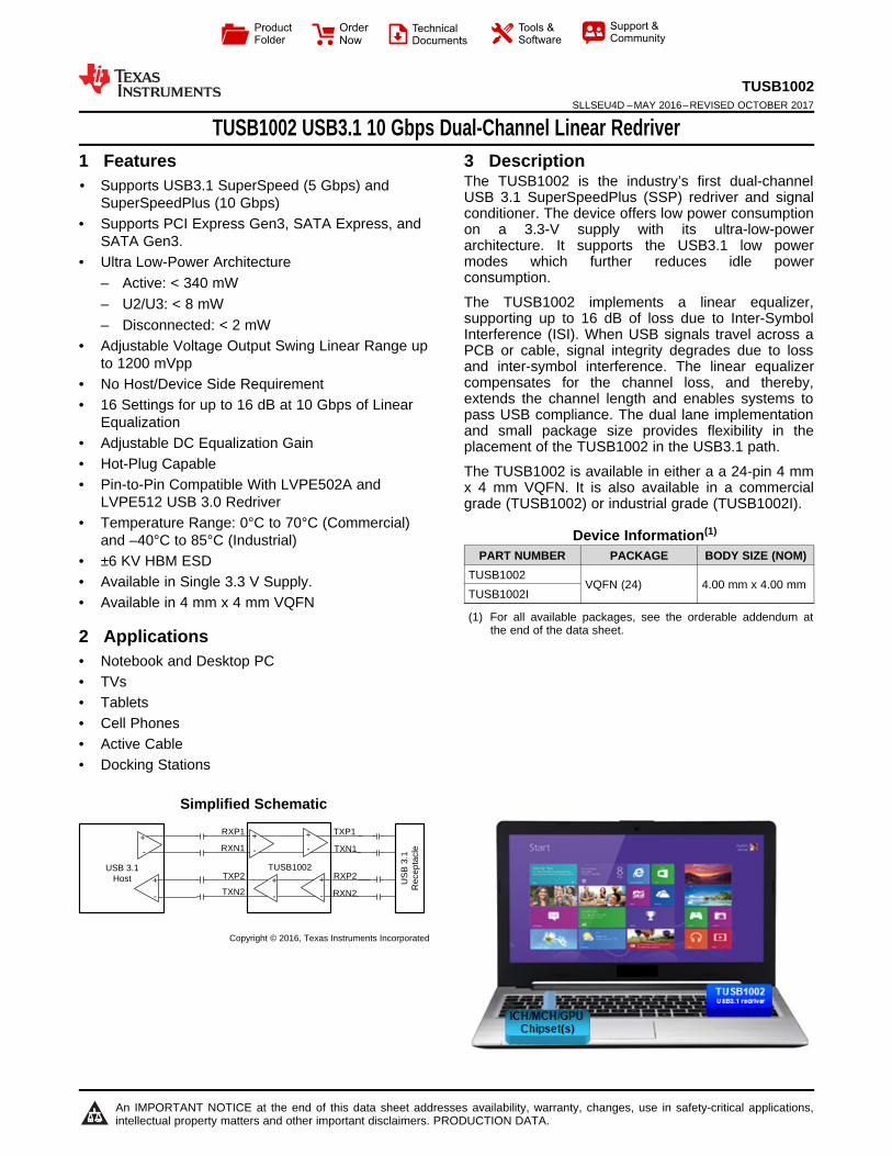
USB 3.1 Host U
SB
3.1
R
ecep
tacl
e
RXP1
TUSB1002
RXN1+
-
TXP2
TXN2+
-
+
-
TXP1
TXN1+
-
+
-
RXP2
RXN2
+
-
Copyright © 2016, Texas Instruments Incorporated
Product
Folder
Order
Now
Technical
Documents
Tools &
Software
Support &Community
An IMPORTANT NOTICE at the end of this data sheet addresses availability, warranty, changes, use in safety-critical applications,intellectual property matters and other important disclaimers. PRODUCTION DATA.
TUSB1002SLLSEU4D –MAY 2016–REVISED OCTOBER 2017
TUSB1002 USB3.1 10 Gbps Dual-Channel Linear Redriver
1
1 Features1• Supports USB3.1 SuperSpeed (5 Gbps) and
SuperSpeedPlus (10 Gbps)• Supports PCI Express Gen3, SATA Express, and
SATA Gen3.• Ultra Low-Power Architecture
– Active: < 340 mW– U2/U3: < 8 mW– Disconnected: < 2 mW
• Adjustable Voltage Output Swing Linear Range upto 1200 mVpp
• No Host/Device Side Requirement• 16 Settings for up to 16 dB at 10 Gbps of Linear
Equalization• Adjustable DC Equalization Gain• Hot-Plug Capable• Pin-to-Pin Compatible With LVPE502A and
LVPE512 USB 3.0 Redriver• Temperature Range: 0°C to 70°C (Commercial)
and –40°C to 85°C (Industrial)• ±6 KV HBM ESD• Available in Single 3.3 V Supply.• Available in 4 mm x 4 mm VQFN
2 Applications• Notebook and Desktop PC• TVs• Tablets• Cell Phones• Active Cable• Docking Stations
3 DescriptionThe TUSB1002 is the industry’s first dual-channelUSB 3.1 SuperSpeedPlus (SSP) redriver and signalconditioner. The device offers low power consumptionon a 3.3-V supply with its ultra-low-powerarchitecture. It supports the USB3.1 low powermodes which further reduces idle powerconsumption.
The TUSB1002 implements a linear equalizer,supporting up to 16 dB of loss due to Inter-SymbolInterference (ISI). When USB signals travel across aPCB or cable, signal integrity degrades due to lossand inter-symbol interference. The linear equalizercompensates for the channel loss, and thereby,extends the channel length and enables systems topass USB compliance. The dual lane implementationand small package size provides flexibility in theplacement of the TUSB1002 in the USB3.1 path.
The TUSB1002 is available in either a a 24-pin 4 mmx 4 mm VQFN. It is also available in a commercialgrade (TUSB1002) or industrial grade (TUSB1002I).
Device Information(1)
PART NUMBER PACKAGE BODY SIZE (NOM)TUSB1002
VQFN (24) 4.00 mm x 4.00 mmTUSB1002I
(1) For all available packages, see the orderable addendum atthe end of the data sheet.
SPACERSimplified Schematic
2
TUSB1002SLLSEU4D –MAY 2016–REVISED OCTOBER 2017 www.ti.com
Product Folder Links: TUSB1002
Submit Documentation Feedback Copyright © 2016–2017, Texas Instruments Incorporated
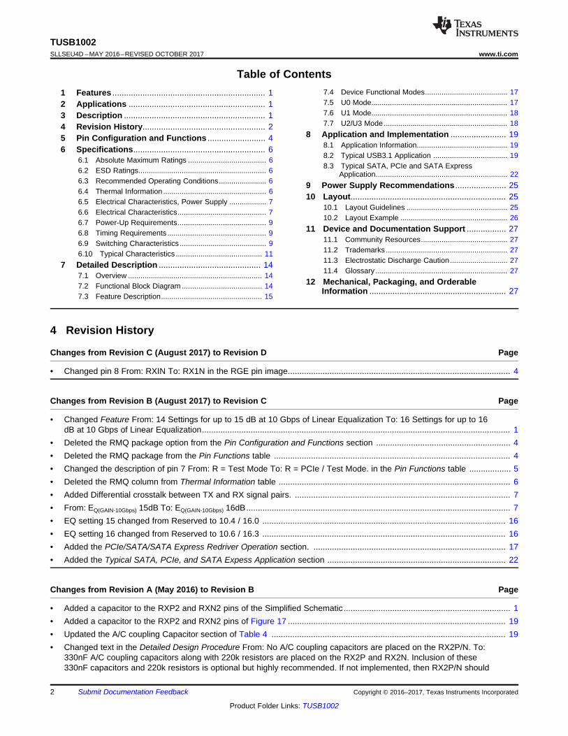
Table of Contents1 Features .................................................................. 12 Applications ........................................................... 13 Description ............................................................. 14 Revision History..................................................... 25 Pin Configuration and Functions ......................... 46 Specifications......................................................... 6
6.1 Absolute Maximum Ratings ...................................... 66.2 ESD Ratings.............................................................. 66.3 Recommended Operating Conditions....................... 66.4 Thermal Information .................................................. 66.5 Electrical Characteristics, Power Supply .................. 76.6 Electrical Characteristics........................................... 76.7 Power-Up Requirements........................................... 96.8 Timing Requirements ................................................ 96.9 Switching Characteristics .......................................... 96.10 Typical Characteristics .......................................... 11
7 Detailed Description ............................................ 147.1 Overview ................................................................. 147.2 Functional Block Diagram ....................................... 147.3 Feature Description................................................. 15
7.4 Device Functional Modes........................................ 177.5 U0 Mode.................................................................. 177.6 U1 Mode.................................................................. 187.7 U2/U3 Mode............................................................ 18
8 Application and Implementation ........................ 198.1 Application Information............................................ 198.2 Typical USB3.1 Application .................................... 198.3 Typical SATA, PCIe and SATA Express
Application................................................................ 229 Power Supply Recommendations ...................... 2510 Layout................................................................... 25
10.1 Layout Guidelines ................................................. 2510.2 Layout Example .................................................... 26
11 Device and Documentation Support ................. 2711.1 Community Resources.......................................... 2711.2 Trademarks ........................................................... 2711.3 Electrostatic Discharge Caution............................ 2711.4 Glossary ................................................................ 27
12 Mechanical, Packaging, and OrderableInformation ........................................................... 27
4 Revision History
Changes from Revision C (August 2017) to Revision D Page
• Changed pin 8 From: RXIN To: RX1N in the RGE pin image................................................................................................ 4
Changes from Revision B (August 2017) to Revision C Page
• Changed Feature From: 14 Settings for up to 15 dB at 10 Gbps of Linear Equalization To: 16 Settings for up to 16dB at 10 Gbps of Linear Equalization..................................................................................................................................... 1
• Deleted the RMQ package option from the Pin Configuration and Functions section .......................................................... 4• Deleted the RMQ package from the Pin Functions table ...................................................................................................... 4• Changed the description of pin 7 From: R = Test Mode To: R = PCIe / Test Mode. in the Pin Functions table .................. 5• Deleted the RMQ column from Thermal Information table .................................................................................................... 6• Added Differential crosstalk between TX and RX signal pairs. ............................................................................................. 7• From: EQ(GAIN-10Gbps) 15dB To: EQ(GAIN-10Gbps) 16dB.................................................................................................................. 7• EQ setting 15 changed from Reserved to 10.4 / 16.0 ......................................................................................................... 16• EQ setting 16 changed from Reserved to 10.6 / 16.3 ......................................................................................................... 16• Added the PCIe/SATA/SATA Express Redriver Operation section. ................................................................................... 17• Added the Typical SATA, PCIe, and SATA Expess Application section ............................................................................. 22
Changes from Revision A (May 2016) to Revision B Page
• Added a capacitor to the RXP2 and RXN2 pins of the Simplified Schematic ........................................................................ 1• Added a capacitor to the RXP2 and RXN2 pins of Figure 17 .............................................................................................. 19• Updated the A/C coupling Capacitor section of Table 4 ..................................................................................................... 19• Changed text in the Detailed Design Procedure From: No A/C coupling capacitors are placed on the RX2P/N. To:
330nF A/C coupling capacitors along with 220k resistors are placed on the RX2P and RX2N. Inclusion of these330nF capacitors and 220k resistors is optional but highly recommended. If not implemented, then RX2P/N should
3
TUSB1002www.ti.com SLLSEU4D –MAY 2016–REVISED OCTOBER 2017
Product Folder Links: TUSB1002
Submit Documentation FeedbackCopyright © 2016–2017, Texas Instruments Incorporated
be DC-coupled to the USB receptacle. ................................................................................................................................ 20• Added 330nF AC capacitors (C12 and C13) on RX2P and RX2N in Figure 18 .................................................................. 20
Changes from Original (May 2016) to Revision A Page
• Changed device status From: Preview To: Production ......................................................................................................... 1
CH
1_E
Q2
54321
RX2P
GND
RX2N
TX1N
CF
G2
VC
C
RX1P
TX2N
TX2P
GND
CH
1_E
Q1
EN
6
7
8
9
10
11
12
131415161718
19
20
21
22
23
24
VC
C
MODERSVD1
GN
D
CH
2_E
Q1
CH
2_E
Q2
SLP
_S0#
GN
D
+-
+-
GF
G1
RX1N
TX1P
4
TUSB1002SLLSEU4D –MAY 2016–REVISED OCTOBER 2017 www.ti.com
Product Folder Links: TUSB1002
Submit Documentation Feedback Copyright © 2016–2017, Texas Instruments Incorporated
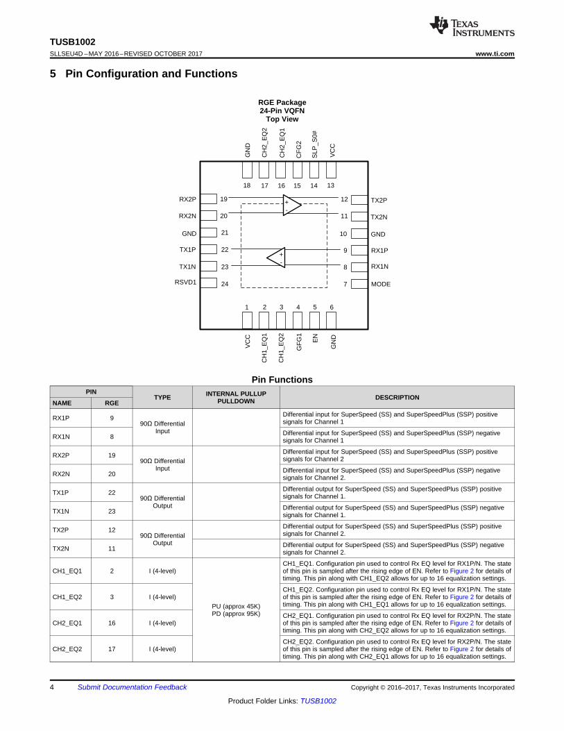
5 Pin Configuration and Functions
RGE Package24-Pin VQFN
Top View
Pin FunctionsPIN
TYPE INTERNAL PULLUPPULLDOWN DESCRIPTION
NAME RGE
RX1P 990Ω Differential
Input
Differential input for SuperSpeed (SS) and SuperSpeedPlus (SSP) positivesignals for Channel 1
RX1N 8 Differential input for SuperSpeed (SS) and SuperSpeedPlus (SSP) negativesignals for Channel 1
RX2P 1990Ω Differential
Input
Differential input for SuperSpeed (SS) and SuperSpeedPlus (SSP) positivesignals for Channel 2
RX2N 20 Differential input for SuperSpeed (SS) and SuperSpeedPlus (SSP) negativesignals for Channel 2.
TX1P 2290Ω Differential
Output
Differential output for SuperSpeed (SS) and SuperSpeedPlus (SSP) positivesignals for Channel 1.
TX1N 23 Differential output for SuperSpeed (SS) and SuperSpeedPlus (SSP) negativesignals for Channel 1.
TX2P 1290Ω Differential
Output
Differential output for SuperSpeed (SS) and SuperSpeedPlus (SSP) positivesignals for Channel 2.
TX2N 11 Differential output for SuperSpeed (SS) and SuperSpeedPlus (SSP) negativesignals for Channel 2.
CH1_EQ1 2 I (4-level)
PU (approx 45K)PD (approx 95K)
CH1_EQ1. Configuration pin used to control Rx EQ level for RX1P/N. The stateof this pin is sampled after the rising edge of EN. Refer to Figure 2 for details oftiming. This pin along with CH1_EQ2 allows for up to 16 equalization settings.
CH1_EQ2 3 I (4-level)CH1_EQ2. Configuration pin used to control Rx EQ level for RX1P/N. The stateof this pin is sampled after the rising edge of EN. Refer to Figure 2 for details oftiming. This pin along with CH1_EQ1 allows for up to 16 equalization settings.
CH2_EQ1 16 I (4-level)CH2_EQ1. Configuration pin used to control Rx EQ level for RX2P/N. The stateof this pin is sampled after the rising edge of EN. Refer to Figure 2 for details oftiming. This pin along with CH2_EQ2 allows for up to 16 equalization settings.
CH2_EQ2 17 I (4-level)CH2_EQ2. Configuration pin used to control Rx EQ level for RX2P/N. The stateof this pin is sampled after the rising edge of EN. Refer to Figure 2 for details oftiming. This pin along with CH2_EQ1 allows for up to 16 equalization settings.
5
TUSB1002www.ti.com SLLSEU4D –MAY 2016–REVISED OCTOBER 2017
Product Folder Links: TUSB1002
Submit Documentation FeedbackCopyright © 2016–2017, Texas Instruments Incorporated
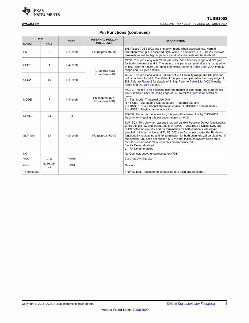
Pin Functions (continued)PIN
TYPE INTERNAL PULLUPPULLDOWN DESCRIPTION
NAME RGE
EN 5 I (2-level) PU (approx 400 K)EN. Places TUSB1002 into shutdown mode when asserted low. Normaloperation when pin is asserted high. When in shutdown, TUSB1002’s receiverterminations will be high impedance and tx/rx channels will be disabled.
CFG1 4 I (4-level)
PU (approx 45K)PD (approx 95K)
CFG1. This pin along with CFG2 will select VOD linearity range and DC gainfor both channels 1 and 2. The state of this pin is sampled after the rising edgeof EN. Refer to Figure 2 for details of timing. Refer to Table 3 for VOD linearityrange and DC gain options.
CFG2 15 I (4-level)
CFG2. This pin along with CFG1 will set VOD linearity range and DC gain forboth channels 1 and 2. The state of this pin is sampled after the rising edge ofEN. Refer to Figure 2 for details of timing. Refer to Table 3 for VOD linearityrange and DC gain options.
MODE 7 I (4-level) PU (approx 45 K)PD (approx 95K)
MODE. This pin is for selecting different modes of operation. The state of thispin is sampled after the rising edge of EN. Refer to Figure 2 for details oftiming.0 = Test Mode. TI Internal Use Only.R = PCIe / Test Mode. PCIe Mode and TI Internal use onlyF = USB3.1 Dual Channel Operation enabled (TUSB1002 normal mode).1 = USB3.1 Single-channel operation.
RSVD1 24 O RSVD1. Under normal operation, this pin will be driven low by TUSB1002.Recommend leaving this pin unconnected on PCB.
SLP_S0# 14 I (2-level) PU (approx 400 K)
SLP_S0#. This pin when asserted low will disable Receiver Detect functionality.While this pin low and TUSB1002 is in U2/U3, TUSB1002 disables LOS andLFPS detection circuitry and Rx termination for both channels will remainenabled. If this pin is low and TUSB1002 is in Disconnect state, the Rx detectfunctionality is disabled and Rx termination for both channels will be disabled. Ifthe system SoC does not support a GPIO that indicates system sleep state,then it is recommended to leave this pin unconnected.0 – Rx Detect disabled1 – Rx Detect enabled
NC No Connect. Leave unconnected on PCB.
VCC 1, 13 Power 3.3 V (±10%) Supply.
GND 6, 10, 18,21 GND Ground
Thermal pad Thermal pad. Recommend connecting to a solid ground plane.
6
TUSB1002SLLSEU4D –MAY 2016–REVISED OCTOBER 2017 www.ti.com
Product Folder Links: TUSB1002
Submit Documentation Feedback Copyright © 2016–2017, Texas Instruments Incorporated
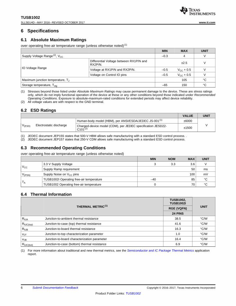
(1) Stresses beyond those listed under Absolute Maximum Ratings may cause permanent damage to the device. These are stress ratingsonly, which do not imply functional operation of the device at these or any other conditions beyond those indicated under RecommendedOperating Conditions. Exposure to absolute-maximum-rated conditions for extended periods may affect device reliability.
(2) All voltage values are with respect to the GND terminal.
6 Specifications
6.1 Absolute Maximum Ratingsover operating free-air temperature range (unless otherwise noted) (1)
MIN MAX UNITSupply Voltage Range (2), VCC –0.3 4 V
IO Voltage Range
Differential Voltage between RX1P/N andRX2P/N. ±2.5 V
Voltage at RX1P/N and RX2P/N. –0.5 VCC + 0.5 VVoltage on Control IO pins –0.5 VCC + 0.5 V
Maximum junction temperature, TJ 105 °CStorage temperature, Tstg –65 150 °C
(1) JEDEC document JEP155 states that 500-V HBM allows safe manufacturing with a standard ESD control process. .(2) JEDEC document JEP157 states that 250-V CDM allows safe manufacturing with a standard ESD control process.
6.2 ESD RatingsVALUE UNIT
V(ESD) Electrostatic dischargeHuman-body model (HBM), per ANSI/ESDA/JEDEC JS-001 (1) ±6000
VCharged-device model (CDM), per JEDEC specification JESD22-C101 (2) ±1500
6.3 Recommended Operating Conditionsover operating free-air temperature range (unless otherwise noted)
MIN NOM MAX UNIT
VCC3.3 V Supply Voltage 3 3.3 3.6 VSupply Ramp requirement 50 ms
V(PSN) Supply Noise on VCC pins 100 mV
TATUSB1002I Operating free-air temperature –40 85 °CTUSB1002 Operating free-air temperature 0 70 °C
(1) For more information about traditional and new thermal metrics, see the Semiconductor and IC Package Thermal Metrics applicationreport.
6.4 Thermal Information
THERMAL METRIC (1)
TUSB1002,TUSB1002I
UNITRGE (VQFN)24 PINS
RθJA Junction-to-ambient thermal resistance 38.5 °C/WRθJC(top) Junction-to-case (top) thermal resistance 41.6 °C/WRθJB Junction-to-board thermal resistance 16.3 °C/WψJT Junction-to-top characterization parameter 1.0 °C/WψJB Junction-to-board characterization parameter 16.4 °C/WRθJC(bot) Junction-to-case (bottom) thermal resistance 6.9 °C/W
7
TUSB1002www.ti.com SLLSEU4D –MAY 2016–REVISED OCTOBER 2017
Product Folder Links: TUSB1002
Submit Documentation FeedbackCopyright © 2016–2017, Texas Instruments Incorporated
6.5 Electrical Characteristics, Power Supplyover operating free-air temperature range (unless otherwise noted)
PARAMETER TEST CONDITIONS MIN TYP MAX UNIT
P(U0_SSP_1200mV)
TUSB1002 power under normal operationin U0 operating a SuperSpeedPlusdatarate with linear range set to 1200mV.
At 10 Gbps; VCC supply stable; VCC = 3.3V; VOD = 1200 mVpp; Pattern = CP9 340 mW
P(U0_SSP_1000mV)
TUSB1002 power under normal operationin U0 operating a SuperSpeedPlusdatarate with linear range set to 1000mV.
At 10 Gbps; VCC supply stable; VCC = 3.3V; VOD = 1000 mVpp; Pattern = CP9 325 mW
P(U0_SSP_900mV)
TUSB1002 power under normal operationin U0 operating a SuperSpeedPlusdatarate with linear range set to 900mV.
At 10 Gbps; VCC supply stable; VCC = 3.3V; VOD = 900 mVpp; Pattern = CP9 298 mW
P(U0_SS_1200mV)TUSB1002 power under normal operationin U0 operating a SuperSpeed datarate.
At 5 Gbps; VCC supply stable; VCC = 3.3 V;VOD = 1200 mVpp; Pattern = CP0. 340 mW
P(U1) TUSB1002 power when U1. In U1; VCC supply stable; VCC = 3.3 V;VOD = 1200 mVpp 340 mW
P(U2U3) TUSB1002 power when in U2/U3. Both channels 1 and 2 in U2/U3; VCCsupply stable; VCC = 3.3 V; 8 mW
P(U2U3_SLP)TUSB1002 power when in U2/U3 andSLP_S0# is low.
Both channels 1 and 2 in U2/U3; VCCsupply stable; VCC = 3.3 V; 0.850 mW
P(DISCONNECT_NONE)
TUSB1002 power when no USB devicedetected on both TX1P/N or TX2P/N.
RX1 and RX2 termination disabled; VCCsupply stable; VCC = 3.3 V 2 mW
P(DISCONNECT_ONE)
TUSB1002 power when a USB devicedetected on either TX1P/N or TX2P/N butnot both.
Either RX1 or RX2 termination enabledboth not both enabled; VCC supply stable;VCC = 3.3 V
5 mW
P(DISCONNECT_SLP)
TUSB1002 power when no USB devicedetected on either TX1P/N or TX2P/N andSLP_S0# is low..
RX1 and RX2 termination disabled; VCCsupply stable; VCC = 3.3 V 0.850 mW
P(SHUTDOWN)TUSB1002 power when EN is assertedlow.; VCC supply stable; VCC = 3.3 V, EN = 0 0.6 mW
6.6 Electrical Characteristicsover operating free-air temperature range (unless otherwise noted)
PARAMETER TEST CONDITIONS MIN TYP MAX UNIT
4-Level Inputs (MODE, CFG1, CFG2,CH1_EQ1, CH1_EQ2, CH2_EQ1, CH2_EQ2 )
IIH High level input current VCC = 3.6 V; VIN = 3.6 V 20 80 μA
IIL Low level input current VCC = 3.6 V; VIN = 0 V –160 –40 μA
VTH Threshold 0 / R
VCC = 3.3 V
0.55 V
Threshold R/ Float 1.65 V
Threshold Float / 1 2.8 V
RPU Internal pull-up resistance 45 kΩ
RPD Internal pull-down resistance 95 kΩ
EN, SLP_S0# Input
VIH High level input voltage VCC = 3. V 1.7 VCC V
VIL Low level input voltage VCC = 3.3 V 0 0.7 V
IIH High level input current VCC = 3.6 V, EN = 3.6 V –10 10 µA
IIL Low level input current VCC = 3.6 V, EN = 0 V –15 15 µA
R(EN-PU)Internal pull-up resistance for EN andSLP_S0#.
400 kΩ
USB3.1 RECEIVER INTERFACE (RX1P/N AND RX2P/N)
RL(RX-DIFF) RX Differential return loss
SDD11 10 MHz at 90 Ω –19 dB
SDD11 2 GHz at 90 Ω –14 dB
SDD11 5 – 10 GHz at 90 Ω –7 dB
RL(RX-CM) RX Common mode return loss 0.5 – 5 GHz at 90 Ω –10 dB
X-TALK Differential crosstalk between TX andRX signal pairs. -50 dB
EQ(GAIN-10Gbps) Equalization Gain 50 mVpp At 5 GHz 16 dB
EQ(DC0) DC Equalization Gain at 0dB setting. 500 mVpp VID at 100 MHz; 1200mVLinear Range Setting; Refer to Table 3
-0.15 dB
8
TUSB1002SLLSEU4D –MAY 2016–REVISED OCTOBER 2017 www.ti.com
Product Folder Links: TUSB1002
Submit Documentation Feedback Copyright © 2016–2017, Texas Instruments Incorporated
Electrical Characteristics (continued)over operating free-air temperature range (unless otherwise noted)
PARAMETER TEST CONDITIONS MIN TYP MAX UNIT
EQ(DC1) DC Equalization Gain at +1dB setting. 500 mVpp VID at 100 MHz; 1200mVLinear Range Setting;
0.80 dB
EQ(DC2) DC Equalization Gain at +2dB setting. 500 mVpp VID at 100 MHz; 1000mVLinear Range Setting;
1.5 dB
EQ(DC-1) DC Equalization Gain at -1dB setting. 500 mVpp VID at 100 MHz; 1200mVLinear Range Setting;
–1.1 dB
EQ(DC-2) DC Equalization Gain at -2dB setting. 500 mVpp VID at 100 MHz; 1200mVLinear Range Setting;
–2.05 dB
V(DIFF_IN)Input differential peak-peak voltageswing range. 2000 mV
V(RX-DC-CM) RX DC common mode voltage 1.65 1.85 2.0 V
R(RX-CM-DC) Receiver DC common mode impedanceMeasured at connector. Present whenSuperSpeed USB device detected onTXP/N
18 30 Ω
R(RX-DIFF-DC) Receiver DC differential impedanceMeasured at connector. Present whenSuperSpeed USB device detected onTXP/N; SLP_S0# = 1;
72 120 Ω
Z(RX-HIGH-IMP-DC-POS)
DC input CM input impedance whentermination is disabled.
Measured at connector. Present whenno SuperSpeed USB device detectedon TXP/N or while VCC is ramping
30 KΩ
V(RX-SIGNAL_DET_DIFF-PP)
Input differential peak-to-peak SignalDetect Assert level
at 10 Gbps. No loss input channel andPRBS7 pattern 92 mV
V(RX-IDLE_DET_DIFF-PP)
Input differential peak-to-peak SignalDetect De-assert Level
at 10 Gbps. No loss input channel andPRBS7 pattern 62 mV
V(RX-LFPS-DET-DIFF-P-P)
LFPS Detect threshold. Below min isnoise.
Measured at connector. Below min issquelched 100 300 mV
V(RX-CM-AC-P) Peak RX AC common mode voltage Measured at package pin 150 mV
C(RX-PARASITIC) Rx Input capacitance for return loss At package pin 0.5 pF
USB3.1 Transmitter Interface (TX1P/N and TX2P/N)
RL(TX-DIFF) TX Differential return loss
SDD22 10MHz – 2 GHz at 90 Ω –15 dB
SDD22 5 GHz at 90 Ω –11 dB
SDD22 5 - 10 GHz at 90 Ω –7 dB
RL(TX-CM) TX Common Mode return loss 0.05 – 5 GHz at 90 Ω –9 dB
V(TX-DIFF-PP_1200)Differential peak-to-peak TX voltageswing linear dynamic range
CFG1 pin = F or 1; Refer to Table 3Measured at -1dB compression point =20log (VOD/VOD_linear)
1200 1450 mV
V(TX-DIFF-PP_1000)Differential peak-to-peak TX voltageswing linear dynamic range
CFG1 pin = R; Refer to Table 3Measured at -1dB compression point =20log (VOD/VOD_linear)
1000 mV
V(TX-DIFF-PP_900)Differential peak-to-peak TX voltageswing linear dynamic range
CFG1 pin = 0; Refer toTable 3Measured at -1dB compressionpoint = 20log (VOD/VOD_linear)
900 mV
V(TX-RCV-DETECT)The amount of voltage change allowedduring Receiver Detection. 600 mV
V(TX-CM-IDLE-DELTA)
Transmitter idle common-mode voltagechange while in U2/3 and not activelytransmitting LFPS.
–600 600 mV
V(TX-DC-CM) TX DC common mode voltage 1200mVpp Linear Range setting. 0 1.85 2 V
V(TX-IDLE-DIFF-AC-PP)
AC Electrical Idle differential peak-to-peak output voltage At package pin. 0 10 mV
V(TX-IDLE-DIFF_DC)DC Electrical Idle differential outputvoltage
At package pin. After low pass filter toremove AC component. 0 14 mV
V(TX-CM-AC-PP)Transmitter AC common mode peak-peak voltage in U0
1200mVpp linear range; CHx_EQsetting matches input channel insertionloss;
80 mV
V(TX-CM-DC-ACTIVE-IDLE-DELTA)
Absolute DC common mode voltagebetween U1 and U0. At package pin. 200 mV
I(TX-SHORT) TX short-circuit current limit 106 mA
R(TX-DC) TX DC common mode impedance At package pin 18 30 Ω
9
TUSB1002www.ti.com SLLSEU4D –MAY 2016–REVISED OCTOBER 2017
Product Folder Links: TUSB1002
Submit Documentation FeedbackCopyright © 2016–2017, Texas Instruments Incorporated
Electrical Characteristics (continued)over operating free-air temperature range (unless otherwise noted)
PARAMETER TEST CONDITIONS MIN TYP MAX UNIT
R(TX-DIFF-DC) TX DC differential impedance 72 90 120 Ω
C(TX-PARASTIC) TX input capacitance for return loss At package pin 0.7 pF
C(AC-COUPLING)External AC Coupling capacitor ondifferential pairs. 75 265 nF
(1) Following pins comprise CFG pins: MODE, CFG1, CFG2, CH1_EQ1, CH1_EQ2, CH2_EQ1, and CH2_EQ2.(2) Internal reset is the AND of EN pin and internal Power Good.
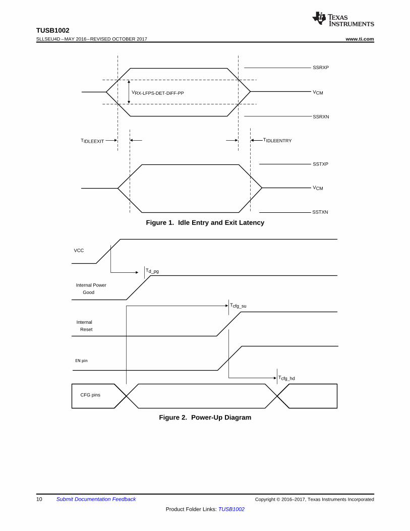
6.7 Power-Up Requirementsover operating free-air temperature range (unless otherwise noted)
PARAMETER MIN MAX UNIT
td_pgInternal Power Good asserted high when VCCis at 2.5 V See Figure 2 5 µs
tcfg_su CFG (1) pins setup before internal Reset (2) high See Figure 2 0 stcfg_hd CFG (1) pins hold after internal Reset (2) high See Figure 2 500 µstVCC_RAMP VCC supply ramp requirement See Figure 2 50 ms
6.8 Timing RequirementsMIN NOM MAX UNIT
SuperSpeed (SS) and SuperSpeedPlus(SSP)tIDLEEntry Delay from U0 to electrical idle. See Figure 1 150 ps
tIDLEExit_U1U1 exit time: break in electrical idle to thetransmission of LFPS. See Figure 1 150 ps
tIDLEExit_U2U3U2/U3 exit time: break in electrical idle totransmission of LFPS See Figure 1 2.3 3.75 µs
tDIFF-DLY Differential propagation delay 150 ps
tPWRUPACTIVETime when VCC reach 2.5 V to deviceactive and performing Rx.Detect. EN = H 7 ms
6.9 Switching Characteristicsover operating free-air temperature range (unless otherwise noted)
PARAMETER TEST CONDITIONS MIN TYP MAX UNITUSB3.1 Transmitter Interface (TX1P/N, TX2P/N)
tTX-RISE-FALL Transmitter rise/fall time 20% to 80% of differential output;1200mVpp linear range setting 40 ps
tRF-MISMATCH Transmitter rise/fall mismatch20% to 80% of differential output;1200mVpp linear range setting;1000mVpp VID;
0.01 UI
tTX-DJ Residual deterministic jitter @10Gbps; 1200mVpp LinearRange Setting 0.08 UI
Td_pg
Internal Power
Good
VCC
Internal
Reset
CFG pins
Tcfg_su
Tcfg_hd
EN pin
SSRXP
SSRXN
SSTXP
SSTXN
VRX-LFPS-DET-DiFF-PP
TIDLEEXIT TIDLEENTRY
VCM
VCM
10
TUSB1002SLLSEU4D –MAY 2016–REVISED OCTOBER 2017 www.ti.com
Product Folder Links: TUSB1002
Submit Documentation Feedback Copyright © 2016–2017, Texas Instruments Incorporated
Figure 1. Idle Entry and Exit Latency
Figure 2. Power-Up Diagram
Frequency (GHz)
SD
D21
(dB
)
-5
0
5
10
15
20
0.01 0.1 1 10
D005
EQ2_DC0_1000mVEQ4_DC0_1000mVEQ6_DC0_1000mVEQ10_DC0_1000mVEQ12_DC0_1000mV
Frequency (GHz)
SD
D21
(dB
)
-5
0
5
10
0.01 0.1 1 10
D006
EQ1_DC0_1000mVEQ1_DC2_1000mVEQ1_DC-1_1000mV
Frequency (GHz)
SD
D21
(dB
)
-5
0
5
10
0.01 0.1 1 10
D003
EQ1_DC0_1200mVEQ1_DC1_1200mVEQ1_DC-1_1200mVEQ1_DC-2_1200mV
Frequency (GHz)
SD
D21
(dB
)
-5
0
5
10
15
20
0.01 0.1 1 10
D004
EQ1_DC0_1000mVEQ3_DC0_1000mVEQ5_DC0_1000mVEQ7_DC0_1000mVEQ9_DC0_1000mVEQ11_DC0_1000mVEQ13_DC0_1000mV
Frequency (GHz)
SD
D21
(dB
)
-5
0
5
10
15
20
0.01 0.1 1 10
D001
EQ1_DC0_1200mVEQ3_DC0_1200mVEQ5_DC0_1200mVEQ7_DC0_1200mVEQ9_DC0_1200mVEQ11_DC0_1200mVEQ13_DC0_1200mV
Frequency (GHz)
SD
D21
(dB
)
-5
0
5
10
15
20
0.01 0.1 1 10
D002
EQ2_DC0_1200mVEQ4_DC0_1200mVEQ6_DC0_1200mVEQ8_DC0_1200mVEQ10_DC0_1200mVEQ12_DC0_1200mVEQ14_DC0_1200mV
11
TUSB1002www.ti.com SLLSEU4D –MAY 2016–REVISED OCTOBER 2017
Product Folder Links: TUSB1002
Submit Documentation FeedbackCopyright © 2016–2017, Texas Instruments Incorporated
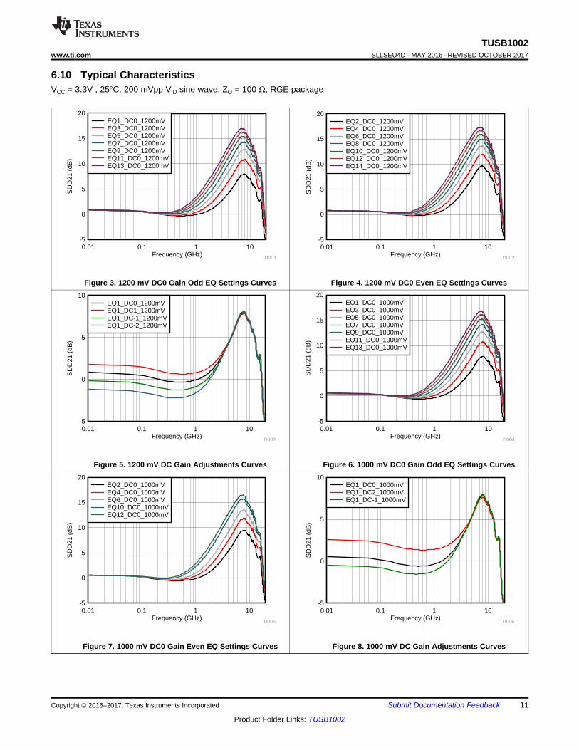
6.10 Typical CharacteristicsVCC = 3.3V , 25°C, 200 mVpp VID sine wave, ZO = 100 Ω, RGE package
Figure 3. 1200 mV DC0 Gain Odd EQ Settings Curves Figure 4. 1200 mV DC0 Even EQ Settings Curves
Figure 5. 1200 mV DC Gain Adjustments Curves Figure 6. 1000 mV DC0 Gain Odd EQ Settings Curves
Figure 7. 1000 mV DC0 Gain Even EQ Settings Curves Figure 8. 1000 mV DC Gain Adjustments Curves
Frequency (GHz)
SD
D22
(dB
)
-40
-35
-30
-25
-20
-15
-10
-5
0
0.01 0.1 1 10
D013VID (V)
VO
D (
V)
0 0.5 1 1.50
0.2
0.4
0.6
0.8
1
1.2
1.4
1.6
D010
DC0_EQ1_900mVDC0_EQ1_1000mVDC0_EQ1_1200mV
Frequency (GHz)
SD
D21
(dB
)
-5
0
5
10
0.01 0.1 1 10
D009
EQ1_DC0_900mVEQ1_DC1_900mV
Frequency (GHz)
SD
D11
(dB
)
-40
-35
-30
-25
-20
-15
-10
-5
0
0.01 0.1 1 10
D012
Frequency (GHz)
SD
D21
(dB
)
-5
0
5
10
15
20
0.01 0.1 1 10
D007
EQ1_DC0_900mVEQ3_DC0_900mVEQ5_DC0_900mVEQ7_DC0_900mVEQ9_DC0_900mVEQ11_DC0_900mVEQ13_DC0_900mV
Frequency (GHz)
SD
D21
(dB
)
-5
0
5
10
15
20
0.01 0.1 1 10
D007
EQ2_DC0_900mVEQ4_DC0_900mVEQ6_DC0_900mVEQ8_DC0_900mVEQ10_DC0_900mVEQ12_DC0_900mVEQ14_DC0_900mV
12
TUSB1002SLLSEU4D –MAY 2016–REVISED OCTOBER 2017 www.ti.com
Product Folder Links: TUSB1002
Submit Documentation Feedback Copyright © 2016–2017, Texas Instruments Incorporated
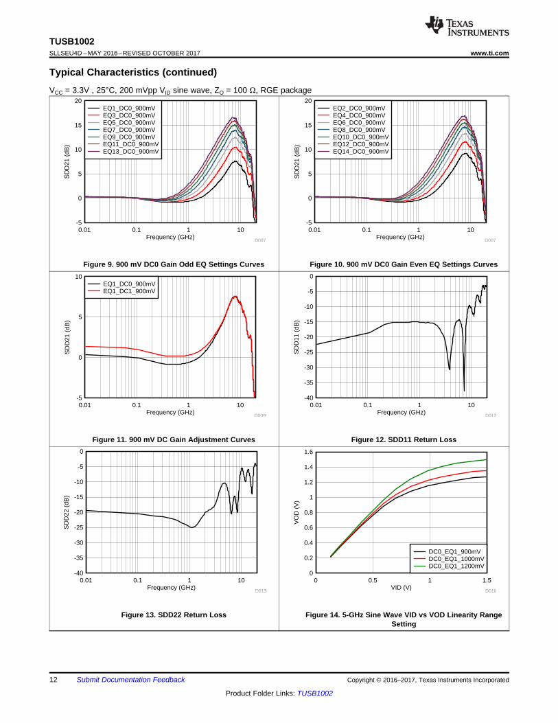
Typical Characteristics (continued)VCC = 3.3V , 25°C, 200 mVpp VID sine wave, ZO = 100 Ω, RGE package
Figure 9. 900 mV DC0 Gain Odd EQ Settings Curves Figure 10. 900 mV DC0 Gain Even EQ Settings Curves
Figure 11. 900 mV DC Gain Adjustment Curves Figure 12. SDD11 Return Loss
Figure 13. SDD22 Return Loss Figure 14. 5-GHz Sine Wave VID vs VOD Linearity RangeSetting
VID (V)
VO
D (
V)
0 0.5 1 1.50
0.2
0.4
0.6
0.8
1
1.2
1.4
D011
DC0_EQ1_900mVDC0_EQ1_1000mVDC0_EQ1_1200mV
13
TUSB1002www.ti.com SLLSEU4D –MAY 2016–REVISED OCTOBER 2017
Product Folder Links: TUSB1002
Submit Documentation FeedbackCopyright © 2016–2017, Texas Instruments Incorporated
Typical Characteristics (continued)VCC = 3.3V , 25°C, 200 mVpp VID sine wave, ZO = 100 Ω, RGE package
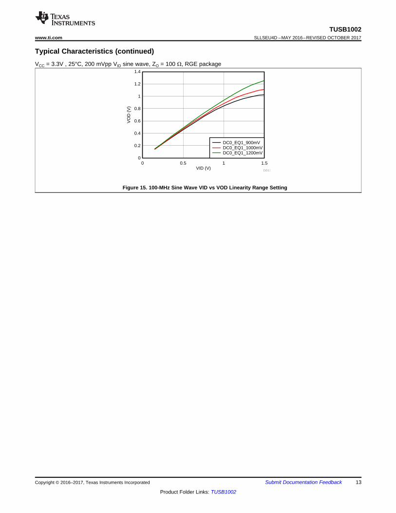
Figure 15. 100-MHz Sine Wave VID vs VOD Linearity Range Setting
CH1_EQ1
CH1_EQ2
SLP_S0#
RX1P
RX1N TX1N
TX1P
50 50
Vterm
VCC
GND
RX TX
VIterm
TXEN1IDLE1
RXDET1LOS
RxDetect
LOSZ1
RXTERM_EN
Digital FSM
RX2P
TX2N
TX2P
5050
Vterm
RXTX
VIterm
TXEN2IDLE2RXDET2
LOS
RxDetect LOSZ2
RXTERM_EN
EN
CH2_EQ1
VCC
PowerManagement
2.5V3.3V (+/-10%)
400K
PG
LFPSLFPS2
LFPS LFPS1
MODE
CFG1
RSVD1
LFPS1LOSZ1
LFPS2LOSZ2
1.2V
CFG2
CH2_EQ2
RX2N
Copyright © 2016, Texas Instruments Incorporated
14
TUSB1002SLLSEU4D –MAY 2016–REVISED OCTOBER 2017 www.ti.com
Product Folder Links: TUSB1002
Submit Documentation Feedback Copyright © 2016–2017, Texas Instruments Incorporated
7 Detailed Description
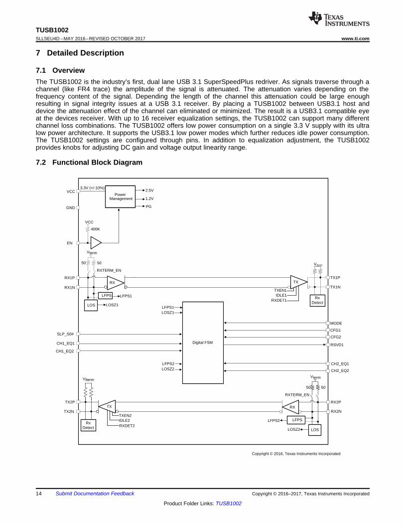
7.1 OverviewThe TUSB1002 is the industry’s first, dual lane USB 3.1 SuperSpeedPlus redriver. As signals traverse through achannel (like FR4 trace) the amplitude of the signal is attenuated. The attenuation varies depending on thefrequency content of the signal. Depending the length of the channel this attenuation could be large enoughresulting in signal integrity issues at a USB 3.1 receiver. By placing a TUSB1002 between USB3.1 host anddevice the attenuation effect of the channel can eliminated or minimized. The result is a USB3.1 compatible eyeat the devices receiver. With up to 16 receiver equalization settings, the TUSB1002 can support many differentchannel loss combinations. The TUSB1002 offers low power consumption on a single 3.3 V supply with its ultralow power architecture. It supports the USB3.1 low power modes which further reduces idle power consumption.The TUSB1002 settings are configured through pins. In addition to equalization adjustment, the TUSB1002provides knobs for adjusting DC gain and voltage output linearity range.
7.2 Functional Block Diagram
15
TUSB1002www.ti.com SLLSEU4D –MAY 2016–REVISED OCTOBER 2017
Product Folder Links: TUSB1002
Submit Documentation FeedbackCopyright © 2016–2017, Texas Instruments Incorporated
7.3 Feature Description
7.3.1 4-Level Control InputsThe TUSB1002 has (MODE, CFG1, CFG2, CH1_EQ1, CH1_EQ2, CH2_EQ1, and CH2_EQ2) 4-level inputs pinsthat are used to control the equalization gain and the output voltage swing dynamic range. These 4-level inputsuse a resistor divider to help set the 4 valid levels and provide a wider range of control settings. There is aninternal 45 kΩ pull-up and a 95 kΩ pull-down. These resistors, together with the external resistor connectioncombine to achieve the desired voltage level.
Table 1. 4-Level Control Pin SettingsLEVEL SETTINGS
0 Option 1: Tie 1 KΩ 5% to GND.Option 2: Tie directly to GND.
R Tie 20 KΩ 5% to GND.F Float (leave pin open)
1 Option 1: Tie 1 KΩ 5% to VCC.Option 2: Tie directly to VCC.
NOTEIn order to conserve power, the TUSB1002 disables 4-level input’s internal pull-up/pull-down resistors after the state of 4-level pins have been sampled on rising edge of EN. Achange of state for any four level input pin is not applied to TUSB1002 until after EN pintransitions from low to high.
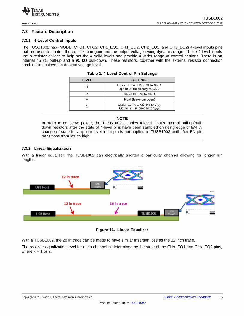
7.3.2 Linear EqualizationWith a linear equalizer, the TUSB1002 can electrically shorten a particular channel allowing for longer runlengths.
Figure 16. Linear Equalizer
With a TUSB1002, the 28 in trace can be made to have similar insertion loss as the 12 inch trace.
The receiver equalization level for each channel is determined by the state of the CHx_EQ1 and CHx_EQ2 pins,where x = 1 or 2.
16
TUSB1002SLLSEU4D –MAY 2016–REVISED OCTOBER 2017 www.ti.com
Product Folder Links: TUSB1002
Submit Documentation Feedback Copyright © 2016–2017, Texas Instruments Incorporated
Table 2. EQ Configuration Options for 1200mV Linearity 0 dB DC Gain Setting
EQ SETTING # CHx_EQ2 PIN LEVEL CHx_EQ1 PIN LEVEL EQ GAIN at 2.5GHz / 5GHz (dB)
1 0 0 1.9 / 5.52 0 R 2.8 / 7.13 0 F 3.5 / 8.24 0 1 4.4 / 9.35 R 0 5.0 / 10.26 R R 5.8 / 11.17 R F 6.4 / 11.88 R 1 7.1 / 12.69 F 0 7.6 / 13.110 F R 8.2 / 13.811 F F 8.7 / 14.312 F 1 9.2 / 14.813 1 0 9.6 / 15.214 1 R 10.1 / 15.615 1 F 10.4 / 16.016 1 1 10.6 / 16.3
7.3.3 Adjustable VOD Linear Range and DC GainThe CFG1 and CFG2 pins can be used to adjust the TUSB1002 output voltage swing linear range and receiverequalization DC gain. Table 3 details the available options.
For best performance, the TUSB1002 should be operated within its defined VOD linearity range. The gain of theincoming VID should be kept to less than or equal to the TUSB1002 VOD linear range setting. The can bedetermined by Equation 1:
VID at 5 GHz = VOD x (10 -(Gv/20))
where• Gv = TUSB1002 Gain and VOD = TUSB100 VOD linearity setting. (1)
For example, for a VOD linearity range setting of 1200 mV, the maximum incoming VID signal at 5 GHz with aCHx_EQ[1:0] setting of 1 (5.5 dB) is 1200 x (10 -(5.5/20)) = 637 mVpp. The TUSB1002 can be operated outside itsVOD linear range but jitter will be higher.
Table 3. VOD Linear Range and DC Gain
SETTING # CFG1 PIN LEVEL CFG2 PIN LEVEL CH1 DC GAIN (dB) CH2 DC GAIN (dB) CH1 VOD LINEARRANGE (mVpp)
CH2 VOD LINEARRANGE (mVpp)
1 0 0 +1 0 900 900
2 0 R 0 +1 900 900
3 0 F 0 0 900 900
4 0 1 +1 +1 900 900
5 R 0 0 0 1000 1000
6 R R +1 0 1000 1000
7 R F 0 -1 1000 1000
8 R 1 +2 +2 1000 1000
9 F 0 -1 -1 1200 1200
10 F R -2 -2 1200 1200
11 F F 0 0 1200 1200
12 F 1 +1 +1 1200 1200
13 1 0 -1 0 1200 1200
14 1 R 0 -1 1200 1200
15 1 F 0 +1 1200 1200
16 1 1 +1 0 1200 1200
17
TUSB1002www.ti.com SLLSEU4D –MAY 2016–REVISED OCTOBER 2017
Product Folder Links: TUSB1002
Submit Documentation FeedbackCopyright © 2016–2017, Texas Instruments Incorporated
7.3.4 Receiver Detect ControlThe SLP_S0# pin offers system designers the ability to control the TUSB1002 Rx.Detect functionality duringDisconnect and U2/U3 states and therefore achieving lower consumption in these states. When the system is ina low power state (Sx where x = 1, 2, 3, 4, or 5), system can assert SLP_S0# low to disable TUSB1002 receiverdetect functionality. While SLP_S0# is asserted low and USB 3.1 interface is in U3, the TUSB1002 keepsreceiver termination active. The TUSB1002 will not respond to any LFPS signaling while in this state. This meansthat system wake from U3 is not supported while SLP_S0# is asserted low. If the TUSB1002 is in Disconnectstate when SLP_S0# is asserted low, then TUSB1002 disables both channels receiver termination. WhenSLP_S0# is asserted high, the TUSB1002 resumes normal operation of performing far-end receiver terminationdetection.
7.3.5 USB3.1 Dual Channel Operation (MODE = “F”)The TUSB1002 in dual-channel operation waits for far-end terminations on both channels 1 and 2 beforetransitioning to fully active state (U0 mode). This mode of operation, defined as MODE pin = ‘F’, is the mostcommon configuration for USB3.1 Source (DFP) and Sink (UFP) applications.
7.3.6 USB3.1 Single Channel Operation (MODE = “1”)In some applications, like Type-C USB3.1 active cables, only one of the two channels may be active. For thisapplication, setting MODE pin = ‘1’, enables single-channel operation. In this mode of operation, the TUSB1002attempts far-end termination on both channels 1 and 2. The channel which has a far-end termination detectedwill be enabled while the remaining channel will be disabled. If far-end termination is detected on both channels,then TUSB1002 behaves in dual channel operation (both channels enabled).
7.3.7 PCIe/SATA/SATA Express Redriver Operation (MODE = “R”; CFG1 = "0"; CFG2 = "0" )The TUSB1002 can be used as a PCI Express (PCIe) Gen3, SATA Gen3, or SATA Express redriver. WhenTUSB1002's MODE pin = “R”, CFG1 pin = "0", and CFG2 pin = "0", the TUSB1002 will enable both channels(upstream and downstream) receiver and transmitter paths upon detecting far-end termination on both TX1 andTX2. Both upstream and downstream paths will remain enabled until EN pin is de-asserted low. All USB3.1power management functionality is disabled in this mode. In this mode the TUSB1002 is transparent to PCIe linkpower management (L0s, L1) and SATA interface power states. Once far-end termination is detected on bothTX1 and TX2, the TUSB1002 power will be at P(U0_SSP_1200mV) regardless of the PCIe or SATA power state. Tosave power during system S3/S4/S5 states it is suggested to de-assert the EN pin to conserve power.
7.4 Device Functional Modes
7.4.1 Shutdown ModeThe Shutdown mode is entered when EN pin is low and VCC is active and stable. This mode is the lowest powerstate of the TUSB1002. While in this mode, the TUSB1002 receiver terminations is disabled.
7.4.2 Disconnect ModeNext to Shutdown Mode, the Disconnect mode is the lowest power state of the TUSB1002. The TUSB1002enters this mode when exiting Shutdown mode. In this state, the TUSB1002 periodically checks for far-endreceiver termination on both SSTX1 and SSTX2. Upon detection of the far-end receiver’s termination on bothports, the TUSB1002 transitions to a fully active mode called U0 mode.
When SLP_S0# is asserted low and the TUSB1002 is in Disconnect mode, the TUSB1002 remains inDisconnect mode and never perform far-end receiver detection. This allows even lower TUSB1002 powerconsumption while in the Disconnect mode. Once SLP_S0# is asserted high, the TUSB1002 again startsperforming far-end receiver detection so it can know when to exit the Disconnect mode.
7.5 U0 ModeThe U0 mode is the highest power state of the TUSB1002. Anytime high-speed traffic (SuperSpeed orSuperSpeedPlus) is being received, the TUSB1002 remains in this mode. The TUSB1002 only exits this mode ifelectrical idle is detected on both SSRX1 and SSRX2. While in this mode, the TUSB1002 hs speed receiversand transmitters are powered and active.
18
TUSB1002SLLSEU4D –MAY 2016–REVISED OCTOBER 2017 www.ti.com
Product Folder Links: TUSB1002
Submit Documentation Feedback Copyright © 2016–2017, Texas Instruments Incorporated
7.6 U1 ModeThe U1 mode is the intermediate mode between U0 mode and U2/U3 mode. In U1 mode, the TUSB1002’sreceiver termination remains enabled and the TXP/N DC common mode is maintained.
7.7 U2/U3 ModeNext to the disconnect mode, the U2/U3 mode is next lowest power state. While in this mode, the TUSB1002periodically performs far-end receiver detection. Anytime the far-end receiver termination is not detected oneither CH1 or CH2, the TUSB1002 leaves the U2/U3 mode and transition to the Disconnect mode. It alsomonitors the SSRX1 and SSRX2 for a valid LFPS. Upon detection of a valid LFPS, the TUSB1002 immediatelytransitions to the U0 mode.
When SLP_S0# is asserted low and the TUSB1002 is in U2/U3 mode, the TUSB1002 remains in U2/U3 stateand never perform far-end receiver detection. While in this state, the TUSB1002 ignores LFPS signaling. Thisallows even lower TUSB1002 power consumption while in the U2/U3 mode. Once SLP_S0# is asserted high, theTUSB1002 again starts performing far-end receive as well as monitor LFPS so it can know when to exit theU2/U3 mode.
A B C DFR4 Trace of Length Y
FR4 Trace of Length X
C
USB 3.1 Host U
SB
3.1
R
ecep
tacl
e
RXP1
TUSB1002
RXN1
+
-
TXP2
TXN2
+
-
+
-
TXP1
TXN1
+
-
+
-
RXP2
RXN2
+
-
Upstream
C
C
C
C
Downstream
Copyright © 2016, Texas Instruments Incorporated
C
C
C
19
TUSB1002www.ti.com SLLSEU4D –MAY 2016–REVISED OCTOBER 2017
Product Folder Links: TUSB1002
Submit Documentation FeedbackCopyright © 2016–2017, Texas Instruments Incorporated
8 Application and Implementation
NOTEInformation in the following applications sections is not part of the TI componentspecification, and TI does not warrant its accuracy or completeness. TI’s customers areresponsible for determining suitability of components for their purposes. Customers shouldvalidate and test their design implementation to confirm system functionality.
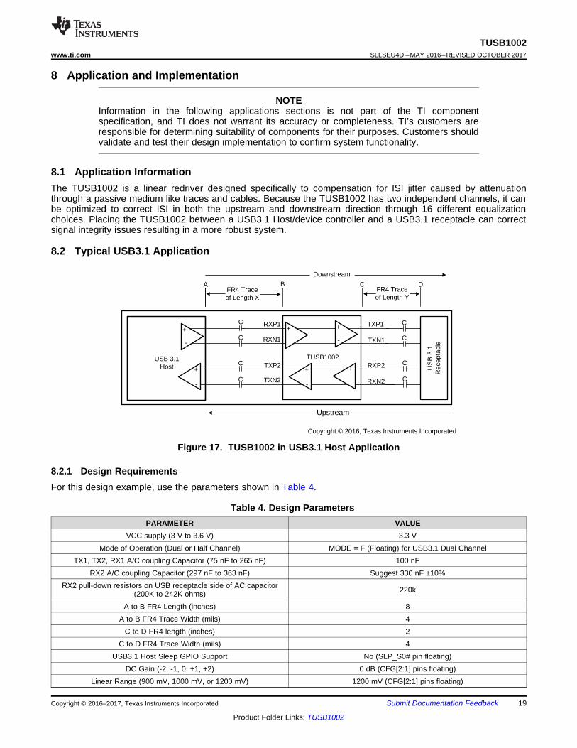
8.1 Application InformationThe TUSB1002 is a linear redriver designed specifically to compensation for ISI jitter caused by attenuationthrough a passive medium like traces and cables. Because the TUSB1002 has two independent channels, it canbe optimized to correct ISI in both the upstream and downstream direction through 16 different equalizationchoices. Placing the TUSB1002 between a USB3.1 Host/device controller and a USB3.1 receptacle can correctsignal integrity issues resulting in a more robust system.
8.2 Typical USB3.1 Application
Figure 17. TUSB1002 in USB3.1 Host Application
8.2.1 Design RequirementsFor this design example, use the parameters shown in Table 4.
Table 4. Design ParametersPARAMETER VALUE
VCC supply (3 V to 3.6 V) 3.3 VMode of Operation (Dual or Half Channel) MODE = F (Floating) for USB3.1 Dual Channel
TX1, TX2, RX1 A/C coupling Capacitor (75 nF to 265 nF) 100 nFRX2 A/C coupling Capacitor (297 nF to 363 nF) Suggest 330 nF ±10%
RX2 pull-down resistors on USB receptacle side of AC capacitor(200K to 242K ohms) 220k
A to B FR4 Length (inches) 8A to B FR4 Trace Width (mils) 4
C to D FR4 length (inches) 2C to D FR4 Trace Width (mils) 4
USB3.1 Host Sleep GPIO Support No (SLP_S0# pin floating)DC Gain (-2, -1, 0, +1, +2) 0 dB (CFG[2:1] pins floating)
Linear Range (900 mV, 1000 mV, or 1200 mV) 1200 mV (CFG[2:1] pins floating)
HOST_TXP
HOST_TXN
HOST_RXPHOST_RXN
CH2_EQ1
CFG2
CH2_EQ2
HOST_DM
HOST_DP
R2DNI
C10100nF
C11100nF
VCC_3P3V
C910uF
TUSB100224-PIN RGE
U1
VC
C
1
CH
1_E
Q1
CH
1_E
Q2
CF
G1
EN
GN
D
MODE7RX1N
8RX1P
9
GND10
TX2N11
TX2P12
VC
C
SLP
_S0#
CF
G2
CH
2_E
Q1
CH
2_E
Q2
GN
D
RX2P
RX2NGND
TX1P
TX1N
RSVD1
GND
C2100nF
C1100nF
C6100nF
C4100nF
J1
USB3_TYPEA_CONNECTER
VBUS 1
DM 2
DP 3
GND 4
SSRXN
5
SSRXP 6
GND 7
SSTXN 8
SSTXP 9
SHIELD0 10
SHIELD1 11
1M
C7100nF
C80.001uF
USB_VBUS
VCC_3P3V
CONNECT TOUSB3.1 HOST
VCC_3P3V
CFG1
CH1_EQ2
CH1_EQ1
19
20
21
22
23
24
25
18 17 16 15 14
VCC_3P3V
2 3 4 5 613
Copyright © 2016, Texas Instruments Incorporated
C3100nF
C5100nF
C12330nF
C13330nF
R1
R16220k
R15220k
20
TUSB1002SLLSEU4D –MAY 2016–REVISED OCTOBER 2017 www.ti.com
Product Folder Links: TUSB1002
Submit Documentation Feedback Copyright © 2016–2017, Texas Instruments Incorporated
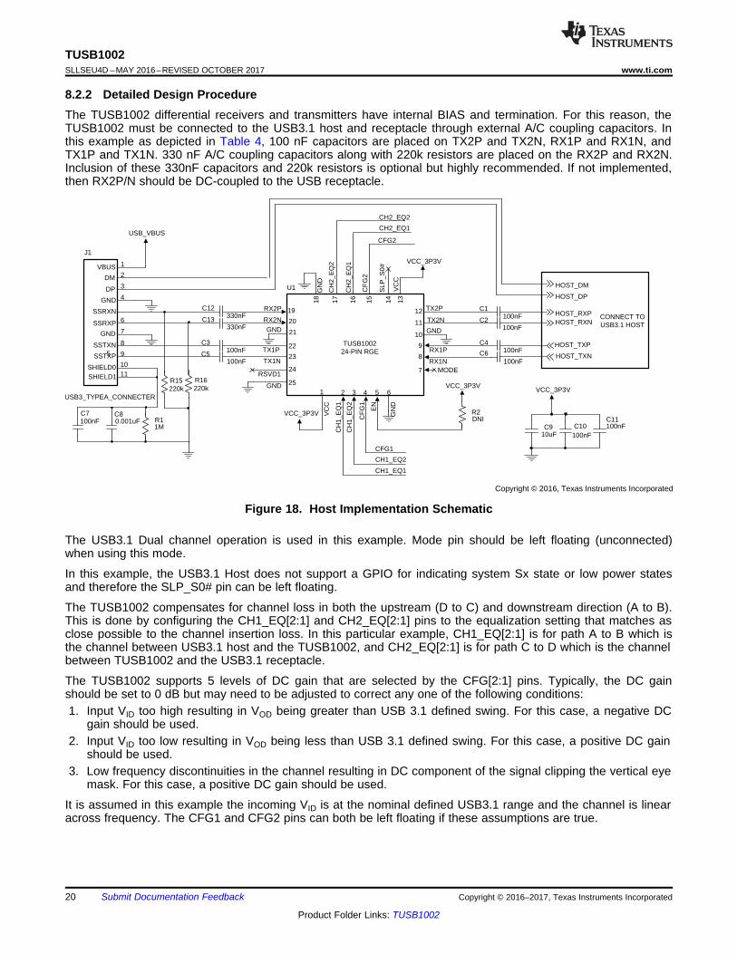
8.2.2 Detailed Design ProcedureThe TUSB1002 differential receivers and transmitters have internal BIAS and termination. For this reason, theTUSB1002 must be connected to the USB3.1 host and receptacle through external A/C coupling capacitors. Inthis example as depicted in Table 4, 100 nF capacitors are placed on TX2P and TX2N, RX1P and RX1N, andTX1P and TX1N. 330 nF A/C coupling capacitors along with 220k resistors are placed on the RX2P and RX2N.Inclusion of these 330nF capacitors and 220k resistors is optional but highly recommended. If not implemented,then RX2P/N should be DC-coupled to the USB receptacle.
Figure 18. Host Implementation Schematic
The USB3.1 Dual channel operation is used in this example. Mode pin should be left floating (unconnected)when using this mode.
In this example, the USB3.1 Host does not support a GPIO for indicating system Sx state or low power statesand therefore the SLP_S0# pin can be left floating.
The TUSB1002 compensates for channel loss in both the upstream (D to C) and downstream direction (A to B).This is done by configuring the CH1_EQ[2:1] and CH2_EQ[2:1] pins to the equalization setting that matches asclose possible to the channel insertion loss. In this particular example, CH1_EQ[2:1] is for path A to B which isthe channel between USB3.1 host and the TUSB1002, and CH2_EQ[2:1] is for path C to D which is the channelbetween TUSB1002 and the USB3.1 receptacle.
The TUSB1002 supports 5 levels of DC gain that are selected by the CFG[2:1] pins. Typically, the DC gainshould be set to 0 dB but may need to be adjusted to correct any one of the following conditions:1. Input VID too high resulting in VOD being greater than USB 3.1 defined swing. For this case, a negative DC
gain should be used.2. Input VID too low resulting in VOD being less than USB 3.1 defined swing. For this case, a positive DC gain
should be used.3. Low frequency discontinuities in the channel resulting in DC component of the signal clipping the vertical eye
mask. For this case, a positive DC gain should be used.
It is assumed in this example the incoming VID is at the nominal defined USB3.1 range and the channel is linearacross frequency. The CFG1 and CFG2 pins can both be left floating if these assumptions are true.
Frequency (GHz)
dB (
SD
D21
)
-30
-25
-20
-15
-10
-5
0
0 2 4 6 8 10 12 14 16 18 20
D100
21
TUSB1002www.ti.com SLLSEU4D –MAY 2016–REVISED OCTOBER 2017
Product Folder Links: TUSB1002
Submit Documentation FeedbackCopyright © 2016–2017, Texas Instruments Incorporated
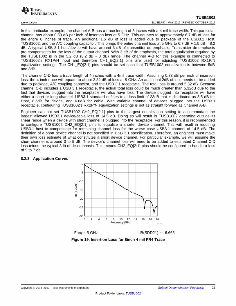
In this particular example, the channel A-B has a trace length of 8 inches with a 4 mil trace width. This particularchannel has about 0.83 dB per inch of insertion loss at 5 GHz. This equates to approximately 6.7 dB of loss forthe entire 8 inches of trace. An additional 1.5 dB of loss is added due to package of the USB3.1 Host,TUSB1002, and the A/C coupling capacitor. This brings the entire channel loss at 5 GHz to 6.7 dB + 1.5 dB = 8.2dB. A typical USB 3.1 host/device will have around 3 dB of transmitter de-emphasis. Transmitter de-emphasispre-compensates for the loss of the output channel. With 3 dB of de-emphasis, the total equalization required bythe TUSB1002 is in the 5.2 dB (8.2 dB - 3 dB) range. The channel A-B for this example is connected toTUSB1002's RX1P/N input and therefore CH1_EQ[2:1] pins are used for adjusting TUSB1002 RX1P/Nequalization settings. The CH1_EQ[2:1] pins should be set such that TUSB1002 equalization is between 5dBand 8dB.
The channel C-D has a trace length of 4 inches with a 4mil trace width. Assuming 0.83 dB per inch of insertionloss, the 4 inch trace will equate to about 3.32 dB of loss at 5 GHz. An additional 2dB of loss needs to be addeddue to package, A/C coupling capacitor, and the USB 3.1 receptacle. The total loss is around 5.32 dB. Becausechannel C-D includes a USB 3.1 receptacle, the actual total loss could be much greater than 5.32dB due to thefact that devices plugged into the receptacle will also have loss. The device plugged into receptacle will haveeither a short or long channel. USB3.1 standard defines total loss limit of 23dB that is distributed as 8.5 dB forHost, 8.5dB for device, and 6.0dB for cable. With variable channel of devices plugged into the USB3.1receptacle, configuring TUSB1002's RX2P/N equalization settings is not as straight forward as Channel A-B.
Engineer can not set TUSB1002 CH2_EQ[2:1] pins to the largest equalization setting to accommodate thelargest allowed USB3.1 device/cable loss of 14.5 dB. Doing so will result in TUSB1002 operating outside itslinear range when a device with short channel is plugged into the receptacle. For this reason, it is recommendedto configure TUSB1002 CH2_EQ[2:1] pins to equalize a shorter device channel. This will result in requiringUSB3.1 host to compensate for remaining channel loss for the worse case USB3.1 channel of 14.5 dB. Thedefinition of a short device channel is not specified in USB 3.1 specification. Therefore, an engineer must maketheir own loss estimate of what constitutes a short device channel. For particular example, we will assume theshort channel is around 3 to 5 dB. The device's channel loss will need to be added to estimated Channel C-Dloss minus the typical 3db of de-emphasis. This means CH2_EQ[2:1] pins should be configured to handle a lossof 5 to 7 db.
8.2.3 Application Curves
Freq = 5 GHz dB(SDD21) = –6.666
Figure 19. Insertion Loss for 8inch 4 mil FR4 Trace
SATA/PCIe/
SATA Express
Host
+
-
+
-
+
-
+
-
RXP2
RXN2
TXP2
TXN2
TUSB1002
+
-
+
-
RXP1
RXN1
TXP1
TXN1
+
-
+
-
SATA/PCIe/SATA Express
Device
min
iCa
rd /
mS
AT
A
sock
et
FR4 trace
of length Y
FR4 trace
of length X
Downstream
Upstream
A B C D
Copyright © 2017, Texas Instruments Incorporated
22
TUSB1002SLLSEU4D –MAY 2016–REVISED OCTOBER 2017 www.ti.com
Product Folder Links: TUSB1002
Submit Documentation Feedback Copyright © 2016–2017, Texas Instruments Incorporated
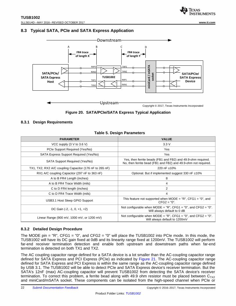
8.3 Typical SATA, PCIe and SATA Express Application
Figure 20. SATA/PCIe/SATA Express Typical Application
8.3.1 Design Requirements
Table 5. Design ParametersPARAMETER VALUE
VCC supply (3 V to 3.6 V) 3.3 VPCIe Support Required (Yes/No) Yes
SATA Express Support Required (Yes/No) Yes
SATA Support Required (Yes/No) Yes, then ferrite beads (FB1 and FB2) and 49.9-ohm required.No, then ferrite bead (FB1 and FB2) and 49.9-ohm not required.
TX1, TX2, RX2 A/C coupling Capacitor (176 nF to 265 nF) 220 nF ±10%RX1 A/C coupling Capacitor (297 nF to 363 nF) Optional. But if implemented suggest 330 nF ±10%
A to B FR4 Length (inches) 8A to B FR4 Trace Width (mils) 4
C to D FR4 length (inches) 2C to D FR4 Trace Width (mils) 4
USB3.1 Host Sleep GPIO Support This feature not supported when MODE = "R", CFG1 = "0", andCFG2 = "0".
DC Gain (-2, -1, 0, +1, +2) Not configurable when MODE = "R", CFG1 = "0", and CFG2 = "0".Will always default to 0 dB
Linear Range (900 mV, 1000 mV, or 1200 mV) Not configurable when MODE = "R", CFG1 = "0", and CFG2 = "0".Will always default to 1200mV
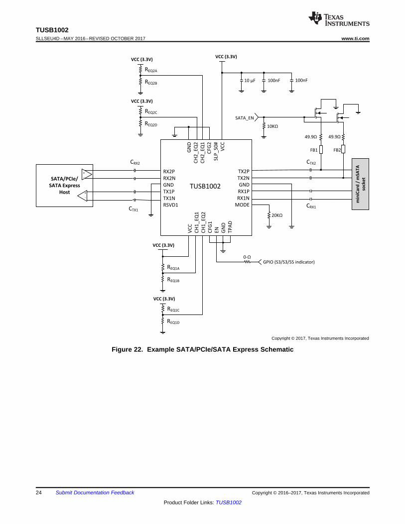
8.3.2 Detailed Design ProcedureThe MODE pin = "R", CFG1 = "0", and CFG2 = "0" will place the TUSB1002 into PCIe mode. In this mode, theTUSB1002 will have its DC gain fixed at 0dB and its linearity range fixed at 1200mV. The TUSB1002 will performfar-end receiver termination detection and enable both upstream and downstream paths when far-endtermination is detected on both TX1 and TX2.
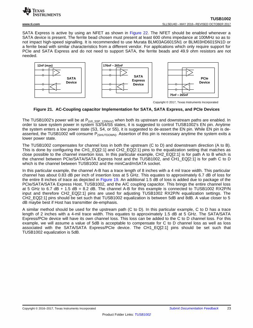
The AC coupling capacitor range defined for a SATA device is a lot smaller than the AC-coupling capacitor rangedefined for SATA Express and PCI Express (PCIe) as indicated by Figure 21. The AC-coupling capacitor rangedefined for SATA Express and PCI Express is within the same range as the AC-coupling capacitor range definedby USB 3.1. The TUSB1002 will be able to detect PCIe and SATA Express device's receiver termination. But theSATA's 12nF (max) AC-coupling capacitor will prevent TUSB1002 from detecting the SATA device's receivertermination. To correct this problem, a ferrite bead along with 49.9 ohm resistor must be placed between CTX2and miniCard/mSATA socket. These components can be isolated from the high-speed channel when PCIe or
+
-
+
-
SATADevice
12nF (max)
+
-
+
-
SATA ExpressDevice
176nF t 265nF
+
-
+
-
PCIeDevice
75nF t 265nF
Copyright © 2017, Texas Instruments Incorporated
23
TUSB1002www.ti.com SLLSEU4D –MAY 2016–REVISED OCTOBER 2017
Product Folder Links: TUSB1002
Submit Documentation FeedbackCopyright © 2016–2017, Texas Instruments Incorporated
SATA Express is active by using an NFET as shown in Figure 22. The NFET should be enabled whenever aSATA device is present. The ferrite bead chosen must present at least 600 ohms impedance at 100MHz so as tonot impact high-speed signalling. It is recommended to use Murata BLM03AG601SN1 or BLM03HD601SN1D ora ferrite bead with similar characteristics from a different vendor. For applications which only require support forPCIe and SATA Express and do not need to support SATA, the ferrite beads and 49.9 ohm resistors are notneeded.
Figure 21. AC-Coupling capacitor Implementation for SATA, SATA Express, and PCIe Devices
The TUSB1002's power will be at P(U0_SSP_1200mV) when both its upstream and downstream paths are enabled. Inorder to save system power in system S3/S4/S5 states, it is suggested to control TUSB1002's EN pin. Anytimethe system enters a low power state (S3, S4, or S5), it is suggested to de-assert the EN pin. While EN pin is de-asserted, the TUSB1002 will consume P(SHUTDOWN). Assertion of this pin is necessary anytime the system exits alower power state.
The TUSB1002 compensates for channel loss in both the upstream (C to D) and downstream direction (A to B).This is done by configuring the CH1_EQ[2:1] and CH2_EQ[2:1] pins to the equalization setting that matches asclose possible to the channel insertion loss. In this particular example, CH2_EQ[2:1] is for path A to B which isthe channel between PCIe/SATA/SATA Express host and the TUSB1002, and CH1_EQ[2:1] is for path C to Dwhich is the channel between TUSB1002 and the miniCard/mSATA socket.
In this particular example, the channel A-B has a trace length of 8 inches with a 4 mil trace width. This particularchannel has about 0.83 dB per inch of insertion loss at 5 GHz. This equates to approximately 6.7 dB of loss forthe entire 8 inches of trace as depicted in Figure 19. An additional 1.5 dB of loss is added due to package of thePCIe/SATA/SATA Express Host, TUSB1002, and the A/C coupling capacitor. This brings the entire channel lossat 5 GHz to 6.7 dB + 1.5 dB = 8.2 dB. The channel A-B for this example is connected to TUSB1002 RX2P/Ninput and therefore CH2_EQ[2:1] pins are used for adjusting TUSB1002 RX2P/N equalization settings. TheCH2_EQ[2:1] pins should be set such that TUSB1002 equalization is between 5dB and 8dB. A value closer to 5dB maybe best if Host has transmitter de-emphasis.
A similar method should be used for the upstream path (C to D). In this particular example, C to D has a tracelength of 2 inches with a 4-mil trace width. This equates to approximately 1.5 dB at 5 GHz. The SATA/SATAExpress/PCIe device will have its own channel loss. This loss can be added to the C to D channel loss. For thisexample, we will assume a value of 5dB is acceptable to compensate for C to D channel loss as well as lossassociated with the SATA/SATA Express/PCIe device. The CH1_EQ[2:1] pins should be set such thatTUSB1002 equalization is 5dB.
SATA/PCIe/
SATA Express
Host
+
-
+
-
min
iCa
rd /
mS
AT
A
sock
et
RX2P
RX2N
GND
TX1P
TX1N
RSVD1
TX2P
TX2N
GND
RX1P
RX1N
MODE
VC
C
CH
1_
EQ
1
CH
1_
EQ
2
CF
G1
EN
GN
D
TP
AD
GN
D
CH
2_
EQ
2
CH
2_
EQ
1
CF
G2
SLP
_S
0#
VC
C
TUSB1002
VCC (3.3V)
VCC (3.3V)
REQ2A
REQ2B
REQ2C
REQ2D
VCC (3.3V)
VCC (3.3V)
REQ1A
REQ1B
REQ1C
REQ1D
20<Q
CRX2
CTX1
CTX2
CRX1
VCC (3.3V)
100nF 100nF10 µF
49.9Q 49.9Q
FB1 FB2
0-QGPIO (S3/S3/S5 indicator)
SATA_EN
10<Q
Copyright © 2017, Texas Instruments Incorporated
24
TUSB1002SLLSEU4D –MAY 2016–REVISED OCTOBER 2017 www.ti.com
Product Folder Links: TUSB1002
Submit Documentation Feedback Copyright © 2016–2017, Texas Instruments Incorporated
Figure 22. Example SATA/PCIe/SATA Express Schematic
25
TUSB1002www.ti.com SLLSEU4D –MAY 2016–REVISED OCTOBER 2017
Product Folder Links: TUSB1002
Submit Documentation FeedbackCopyright © 2016–2017, Texas Instruments Incorporated
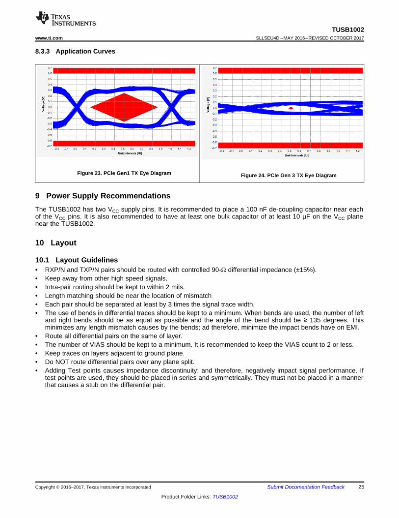
8.3.3 Application Curves
Figure 23. PCIe Gen1 TX Eye Diagram Figure 24. PCIe Gen 3 TX Eye Diagram
9 Power Supply RecommendationsThe TUSB1002 has two VCC supply pins. It is recommended to place a 100 nF de-coupling capacitor near eachof the VCC pins. It is also recommended to have at least one bulk capacitor of at least 10 µF on the VCC planenear the TUSB1002.
10 Layout
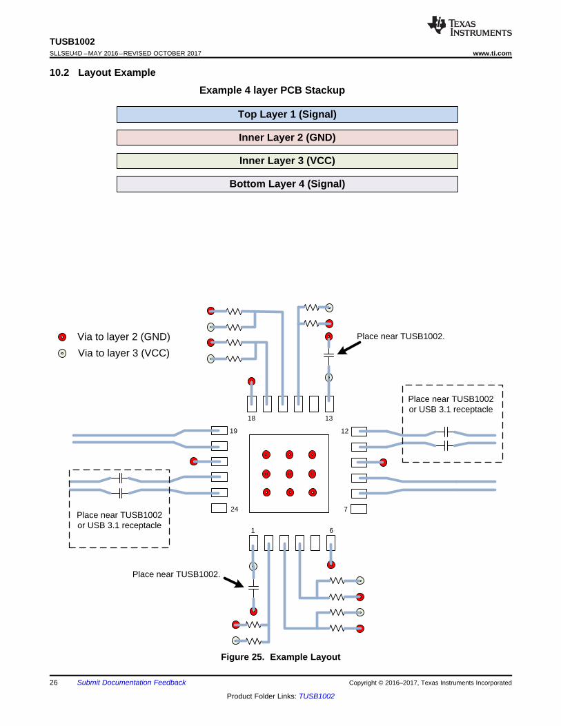
10.1 Layout Guidelines• RXP/N and TXP/N pairs should be routed with controlled 90-Ω differential impedance (±15%).• Keep away from other high speed signals.• Intra-pair routing should be kept to within 2 mils.• Length matching should be near the location of mismatch• Each pair should be separated at least by 3 times the signal trace width.• The use of bends in differential traces should be kept to a minimum. When bends are used, the number of left
and right bends should be as equal as possible and the angle of the bend should be ≥ 135 degrees. Thisminimizes any length mismatch causes by the bends; ad therefore, minimize the impact bends have on EMI.
• Route all differential pairs on the same of layer.• The number of VIAS should be kept to a minimum. It is recommended to keep the VIAS count to 2 or less.• Keep traces on layers adjacent to ground plane.• Do NOT route differential pairs over any plane split.• Adding Test points causes impedance discontinuity; and therefore, negatively impact signal performance. If
test points are used, they should be placed in series and symmetrically. They must not be placed in a mannerthat causes a stub on the differential pair.
Top Layer 1 (Signal)
Inner Layer 2 (GND)
Inner Layer 3 (VCC)
Bottom Layer 4 (Signal)
Example 4 layer PCB Stackup
Via to layer 2 (GND)
1 6
7
12
1318
19
24
Via to layer 3 (VCC)
Place near TUSB1002 or USB 3.1 receptacle
Place near TUSB1002 or USB 3.1 receptacle
Place near TUSB1002.
Place near TUSB1002.
26
TUSB1002SLLSEU4D –MAY 2016–REVISED OCTOBER 2017 www.ti.com
Product Folder Links: TUSB1002
Submit Documentation Feedback Copyright © 2016–2017, Texas Instruments Incorporated
10.2 Layout Example
Figure 25. Example Layout
27
TUSB1002www.ti.com SLLSEU4D –MAY 2016–REVISED OCTOBER 2017
Product Folder Links: TUSB1002
Submit Documentation FeedbackCopyright © 2016–2017, Texas Instruments Incorporated
11 Device and Documentation Support
11.1 Community ResourcesThe following links connect to TI community resources. Linked contents are provided "AS IS" by the respectivecontributors. They do not constitute TI specifications and do not necessarily reflect TI's views; see TI's Terms ofUse.
TI E2E™ Online Community TI's Engineer-to-Engineer (E2E) Community. Created to foster collaborationamong engineers. At e2e.ti.com, you can ask questions, share knowledge, explore ideas and helpsolve problems with fellow engineers.
Design Support TI's Design Support Quickly find helpful E2E forums along with design support tools andcontact information for technical support.
11.2 TrademarksE2E is a trademark of Texas Instruments.All other trademarks are the property of their respective owners.
11.3 Electrostatic Discharge CautionThese devices have limited built-in ESD protection. The leads should be shorted together or the device placed in conductive foamduring storage or handling to prevent electrostatic damage to the MOS gates.
11.4 GlossarySLYZ022 — TI Glossary.
This glossary lists and explains terms, acronyms, and definitions.
12 Mechanical, Packaging, and Orderable InformationThe following pages include mechanical, packaging, and orderable information. This information is the mostcurrent data available for the designated devices. This data is subject to change without notice and revision ofthis document. For browser-based versions of this data sheet, refer to the left-hand navigation.
PACKAGE OPTION ADDENDUM
www.ti.com 26-Oct-2017
Addendum-Page 1
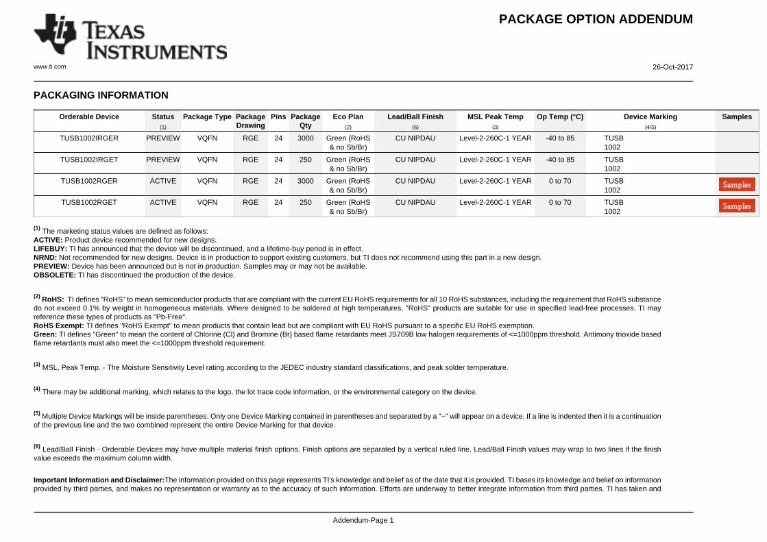
PACKAGING INFORMATION
Orderable Device Status(1)
Package Type PackageDrawing
Pins PackageQty
Eco Plan(2)
Lead/Ball Finish(6)
MSL Peak Temp(3)
Op Temp (°C) Device Marking(4/5)
Samples
TUSB1002IRGER PREVIEW VQFN RGE 24 3000 Green (RoHS& no Sb/Br)
CU NIPDAU Level-2-260C-1 YEAR -40 to 85 TUSB1002
TUSB1002IRGET PREVIEW VQFN RGE 24 250 Green (RoHS& no Sb/Br)
CU NIPDAU Level-2-260C-1 YEAR -40 to 85 TUSB1002
TUSB1002RGER ACTIVE VQFN RGE 24 3000 Green (RoHS& no Sb/Br)
CU NIPDAU Level-2-260C-1 YEAR 0 to 70 TUSB1002
TUSB1002RGET ACTIVE VQFN RGE 24 250 Green (RoHS& no Sb/Br)
CU NIPDAU Level-2-260C-1 YEAR 0 to 70 TUSB1002
(1) The marketing status values are defined as follows:ACTIVE: Product device recommended for new designs.LIFEBUY: TI has announced that the device will be discontinued, and a lifetime-buy period is in effect.NRND: Not recommended for new designs. Device is in production to support existing customers, but TI does not recommend using this part in a new design.PREVIEW: Device has been announced but is not in production. Samples may or may not be available.OBSOLETE: TI has discontinued the production of the device.
(2) RoHS: TI defines "RoHS" to mean semiconductor products that are compliant with the current EU RoHS requirements for all 10 RoHS substances, including the requirement that RoHS substancedo not exceed 0.1% by weight in homogeneous materials. Where designed to be soldered at high temperatures, "RoHS" products are suitable for use in specified lead-free processes. TI mayreference these types of products as "Pb-Free".RoHS Exempt: TI defines "RoHS Exempt" to mean products that contain lead but are compliant with EU RoHS pursuant to a specific EU RoHS exemption.Green: TI defines "Green" to mean the content of Chlorine (Cl) and Bromine (Br) based flame retardants meet JS709B low halogen requirements of <=1000ppm threshold. Antimony trioxide basedflame retardants must also meet the <=1000ppm threshold requirement.
(3) MSL, Peak Temp. - The Moisture Sensitivity Level rating according to the JEDEC industry standard classifications, and peak solder temperature.
(4) There may be additional marking, which relates to the logo, the lot trace code information, or the environmental category on the device.
(5) Multiple Device Markings will be inside parentheses. Only one Device Marking contained in parentheses and separated by a "~" will appear on a device. If a line is indented then it is a continuationof the previous line and the two combined represent the entire Device Marking for that device.
(6) Lead/Ball Finish - Orderable Devices may have multiple material finish options. Finish options are separated by a vertical ruled line. Lead/Ball Finish values may wrap to two lines if the finishvalue exceeds the maximum column width.
Important Information and Disclaimer:The information provided on this page represents TI's knowledge and belief as of the date that it is provided. TI bases its knowledge and belief on informationprovided by third parties, and makes no representation or warranty as to the accuracy of such information. Efforts are underway to better integrate information from third parties. TI has taken and
PACKAGE OPTION ADDENDUM
www.ti.com 26-Oct-2017
Addendum-Page 2
continues to take reasonable steps to provide representative and accurate information but may not have conducted destructive testing or chemical analysis on incoming materials and chemicals.TI and TI suppliers consider certain information to be proprietary, and thus CAS numbers and other limited information may not be available for release.
In no event shall TI's liability arising out of such information exceed the total purchase price of the TI part(s) at issue in this document sold by TI to Customer on an annual basis.
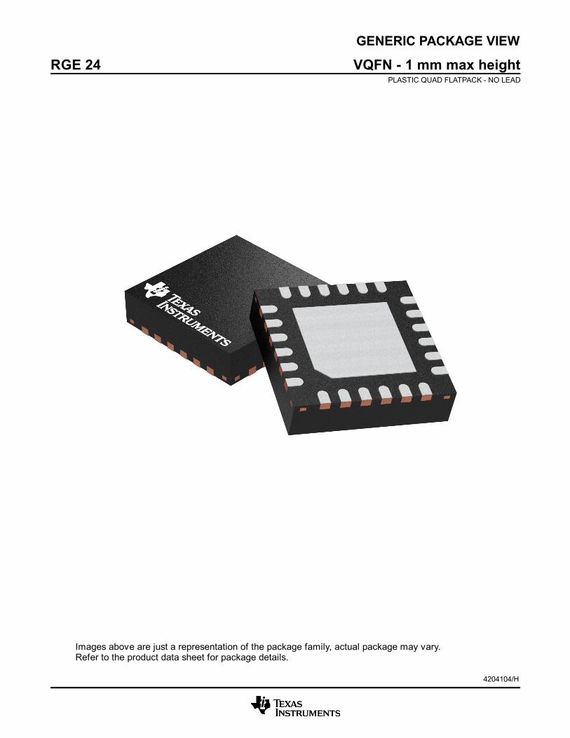
GENERIC PACKAGE VIEW
Images above are just a representation of the package family, actual package may vary.Refer to the product data sheet for package details.
RGE 24 VQFN - 1 mm max heightPLASTIC QUAD FLATPACK - NO LEAD
4204104/H
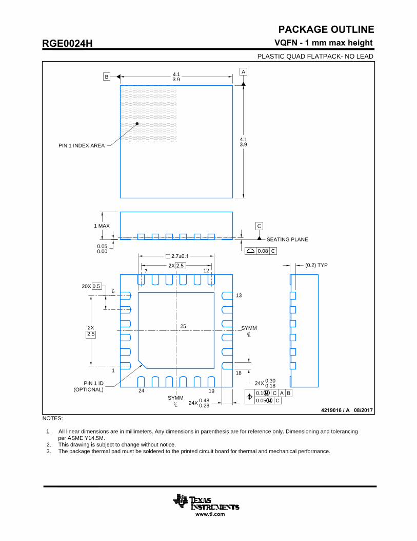
NOTES:
1. All linear dimensions are in millimeters. Any dimensions in parenthesis are for reference only. Dimensioning and tolerancing
per ASME Y14.5M.
2. This drawing is subject to change without notice.
3. The package thermal pad must be soldered to the printed circuit board for thermal and mechanical performance.
PACKAGE OUTLINE
www.ti.com
4219016 / A 08/2017
VQFN - 1 mm max height
PLASTIC QUAD FLATPACK- NO LEAD
RGE0024H
A
0.08 C
0.1 C A B
0.05 C
B
SYMM
SYMM
4.1
3.9
4.1
3.9
PIN 1 INDEX AREA
1 MAX
0.05
0.00
SEATING PLANE
C
2X 2.5
2.7±0.1
2X
2.5
20X 0.5
1
6
7
12
13
18
19
24
24X
0.30
0.18
24X
0.48
0.28
(0.2) TYP
PIN 1 ID
(OPTIONAL)
25
NOTES: (continued)
4. This package is designed to be soldered to a thermal pad on the board. For more information, see Texas Instruments
literature number SLUA271 (www.ti.com/lit/slua271).5. Solder mask tolerances between and around signal pads can vary based on board fabrication site.
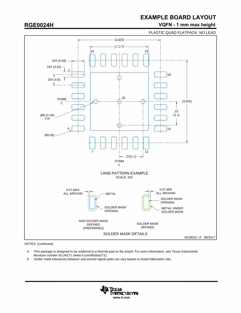
EXAMPLE BOARD LAYOUT
4219016 / A 08/2017
www.ti.com
VQFN - 1 mm max height
RGE0024H
PLASTIC QUAD FLATPACK- NO LEAD
SYMM
SYMM
LAND PATTERN EXAMPLE
SCALE: 20X
2X
(1.1)
2X(1.1)
(3.825)
(3.825)
( 2.7)
1
6
7 12
13
18
1924
25
24X (0.58)
24X (0.24)
20X (0.5)
(R0.05)
(Ø0.2) VIA
TYP
SOLDER MASK DETAILS
NON SOLDER MASK
DEFINED
(PREFERRED)
SOLDER MASK
DEFINED
0.07 MAX
ALL AROUND
0.07 MIN
ALL AROUND
METAL
SOLDER MASK
OPENING
SOLDER MASK
OPENING
METAL UNDER
SOLDER MASK
NOTES: (continued)
6. Laser cutting apertures with trapezoidal walls and rounded corners may offer better paste release. IPC-7525 may have alternate
design recommendations..
EXAMPLE STENCIL DESIGN
4219016 / A 08/2017
www.ti.com
VQFN - 1 mm max height
RGE0024H
PLASTIC QUAD FLATPACK- NO LEAD
SYMM
SYMM
SOLDER PASTE EXAMPLE
BASED ON 0.125 mm THICK STENCIL
EXPOSED PAD
78% PRINTED COVERAGE BY AREA
SCALE: 20X
(3.825)
(3.825)
(0.694)
TYP
(0.694)
TYP
4X ( 1.188)
1
6
712
13
18
1924
24X (0.24)
24X (0.58)
20X (0.5)
(R0.05) TYP
METAL
TYP
25
IMPORTANT NOTICE
Texas Instruments Incorporated (TI) reserves the right to make corrections, enhancements, improvements and other changes to itssemiconductor products and services per JESD46, latest issue, and to discontinue any product or service per JESD48, latest issue. Buyersshould obtain the latest relevant information before placing orders and should verify that such information is current and complete.TI’s published terms of sale for semiconductor products (http://www.ti.com/sc/docs/stdterms.htm) apply to the sale of packaged integratedcircuit products that TI has qualified and released to market. Additional terms may apply to the use or sale of other types of TI products andservices.Reproduction of significant portions of TI information in TI data sheets is permissible only if reproduction is without alteration and isaccompanied by all associated warranties, conditions, limitations, and notices. TI is not responsible or liable for such reproduceddocumentation. Information of third parties may be subject to additional restrictions. Resale of TI products or services with statementsdifferent from or beyond the parameters stated by TI for that product or service voids all express and any implied warranties for theassociated TI product or service and is an unfair and deceptive business practice. TI is not responsible or liable for any such statements.Buyers and others who are developing systems that incorporate TI products (collectively, “Designers”) understand and agree that Designersremain responsible for using their independent analysis, evaluation and judgment in designing their applications and that Designers havefull and exclusive responsibility to assure the safety of Designers' applications and compliance of their applications (and of all TI productsused in or for Designers’ applications) with all applicable regulations, laws and other applicable requirements. Designer represents that, withrespect to their applications, Designer has all the necessary expertise to create and implement safeguards that (1) anticipate dangerousconsequences of failures, (2) monitor failures and their consequences, and (3) lessen the likelihood of failures that might cause harm andtake appropriate actions. Designer agrees that prior to using or distributing any applications that include TI products, Designer willthoroughly test such applications and the functionality of such TI products as used in such applications.TI’s provision of technical, application or other design advice, quality characterization, reliability data or other services or information,including, but not limited to, reference designs and materials relating to evaluation modules, (collectively, “TI Resources”) are intended toassist designers who are developing applications that incorporate TI products; by downloading, accessing or using TI Resources in anyway, Designer (individually or, if Designer is acting on behalf of a company, Designer’s company) agrees to use any particular TI Resourcesolely for this purpose and subject to the terms of this Notice.TI’s provision of TI Resources does not expand or otherwise alter TI’s applicable published warranties or warranty disclaimers for TIproducts, and no additional obligations or liabilities arise from TI providing such TI Resources. TI reserves the right to make corrections,enhancements, improvements and other changes to its TI Resources. TI has not conducted any testing other than that specificallydescribed in the published documentation for a particular TI Resource.Designer is authorized to use, copy and modify any individual TI Resource only in connection with the development of applications thatinclude the TI product(s) identified in such TI Resource. NO OTHER LICENSE, EXPRESS OR IMPLIED, BY ESTOPPEL OR OTHERWISETO ANY OTHER TI INTELLECTUAL PROPERTY RIGHT, AND NO LICENSE TO ANY TECHNOLOGY OR INTELLECTUAL PROPERTYRIGHT OF TI OR ANY THIRD PARTY IS GRANTED HEREIN, including but not limited to any patent right, copyright, mask work right, orother intellectual property right relating to any combination, machine, or process in which TI products or services are used. Informationregarding or referencing third-party products or services does not constitute a license to use such products or services, or a warranty orendorsement thereof. Use of TI Resources may require a license from a third party under the patents or other intellectual property of thethird party, or a license from TI under the patents or other intellectual property of TI.TI RESOURCES ARE PROVIDED “AS IS” AND WITH ALL FAULTS. TI DISCLAIMS ALL OTHER WARRANTIES ORREPRESENTATIONS, EXPRESS OR IMPLIED, REGARDING RESOURCES OR USE THEREOF, INCLUDING BUT NOT LIMITED TOACCURACY OR COMPLETENESS, TITLE, ANY EPIDEMIC FAILURE WARRANTY AND ANY IMPLIED WARRANTIES OFMERCHANTABILITY, FITNESS FOR A PARTICULAR PURPOSE, AND NON-INFRINGEMENT OF ANY THIRD PARTY INTELLECTUALPROPERTY RIGHTS. TI SHALL NOT BE LIABLE FOR AND SHALL NOT DEFEND OR INDEMNIFY DESIGNER AGAINST ANY CLAIM,INCLUDING BUT NOT LIMITED TO ANY INFRINGEMENT CLAIM THAT RELATES TO OR IS BASED ON ANY COMBINATION OFPRODUCTS EVEN IF DESCRIBED IN TI RESOURCES OR OTHERWISE. IN NO EVENT SHALL TI BE LIABLE FOR ANY ACTUAL,DIRECT, SPECIAL, COLLATERAL, INDIRECT, PUNITIVE, INCIDENTAL, CONSEQUENTIAL OR EXEMPLARY DAMAGES INCONNECTION WITH OR ARISING OUT OF TI RESOURCES OR USE THEREOF, AND REGARDLESS OF WHETHER TI HAS BEENADVISED OF THE POSSIBILITY OF SUCH DAMAGES.Unless TI has explicitly designated an individual product as meeting the requirements of a particular industry standard (e.g., ISO/TS 16949and ISO 26262), TI is not responsible for any failure to meet such industry standard requirements.Where TI specifically promotes products as facilitating functional safety or as compliant with industry functional safety standards, suchproducts are intended to help enable customers to design and create their own applications that meet applicable functional safety standardsand requirements. Using products in an application does not by itself establish any safety features in the application. Designers mustensure compliance with safety-related requirements and standards applicable to their applications. Designer may not use any TI products inlife-critical medical equipment unless authorized officers of the parties have executed a special contract specifically governing such use.Life-critical medical equipment is medical equipment where failure of such equipment would cause serious bodily injury or death (e.g., lifesupport, pacemakers, defibrillators, heart pumps, neurostimulators, and implantables). Such equipment includes, without limitation, allmedical devices identified by the U.S. Food and Drug Administration as Class III devices and equivalent classifications outside the U.S.TI may expressly designate certain products as completing a particular qualification (e.g., Q100, Military Grade, or Enhanced Product).Designers agree that it has the necessary expertise to select the product with the appropriate qualification designation for their applicationsand that proper product selection is at Designers’ own risk. Designers are solely responsible for compliance with all legal and regulatoryrequirements in connection with such selection.Designer will fully indemnify TI and its representatives against any damages, costs, losses, and/or liabilities arising out of Designer’s non-compliance with the terms and provisions of this Notice.
Mailing Address: Texas Instruments, Post Office Box 655303, Dallas, Texas 75265Copyright © 2018, Texas Instruments Incorporated