Embed Size (px)
Citation preview
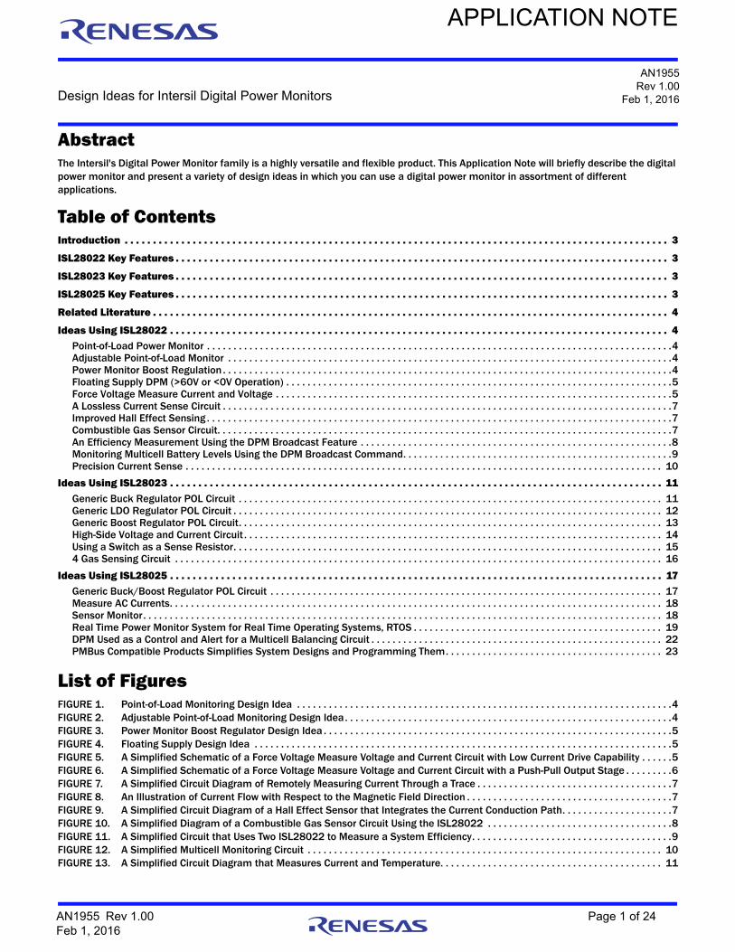
Design Ideas for Intersil Digital Power Monitors
APPLICATION NOTE
AN1955 Rev 1.00Feb 1, 2016
AN1955Rev 1.00
Feb 1, 2016
AbstractThe Intersil's Digital Power Monitor family is a highly versatile and flexible product. This Application Note will briefly describe the digital power monitor and present a variety of design ideas in which you can use a digital power monitor in assortment of different applications.
Table of ContentsIntroduction . . . . . . . . . . . . . . . . . . . . . . . . . . . . . . . . . . . . . . . . . . . . . . . . . . . . . . . . . . . . . . . . . . . . . . . . . . . . . . . . . . . . . . . . . . . . . . . . 3
ISL28022 Key Features . . . . . . . . . . . . . . . . . . . . . . . . . . . . . . . . . . . . . . . . . . . . . . . . . . . . . . . . . . . . . . . . . . . . . . . . . . . . . . . . . . . . . . . 3
ISL28023 Key Features . . . . . . . . . . . . . . . . . . . . . . . . . . . . . . . . . . . . . . . . . . . . . . . . . . . . . . . . . . . . . . . . . . . . . . . . . . . . . . . . . . . . . . . 3
ISL28025 Key Features . . . . . . . . . . . . . . . . . . . . . . . . . . . . . . . . . . . . . . . . . . . . . . . . . . . . . . . . . . . . . . . . . . . . . . . . . . . . . . . . . . . . . . . 3
Related Literature . . . . . . . . . . . . . . . . . . . . . . . . . . . . . . . . . . . . . . . . . . . . . . . . . . . . . . . . . . . . . . . . . . . . . . . . . . . . . . . . . . . . . . . . . . . 4
Ideas Using ISL28022 . . . . . . . . . . . . . . . . . . . . . . . . . . . . . . . . . . . . . . . . . . . . . . . . . . . . . . . . . . . . . . . . . . . . . . . . . . . . . . . . . . . . . . . . 4Point-of-Load Power Monitor . . . . . . . . . . . . . . . . . . . . . . . . . . . . . . . . . . . . . . . . . . . . . . . . . . . . . . . . . . . . . . . . . . . . . . . . . . . . . . . . . . . . . . . .4Adjustable Point-of-Load Monitor . . . . . . . . . . . . . . . . . . . . . . . . . . . . . . . . . . . . . . . . . . . . . . . . . . . . . . . . . . . . . . . . . . . . . . . . . . . . . . . . . . . .4Power Monitor Boost Regulation . . . . . . . . . . . . . . . . . . . . . . . . . . . . . . . . . . . . . . . . . . . . . . . . . . . . . . . . . . . . . . . . . . . . . . . . . . . . . . . . . . . . .4Floating Supply DPM (>60V or <0V Operation) . . . . . . . . . . . . . . . . . . . . . . . . . . . . . . . . . . . . . . . . . . . . . . . . . . . . . . . . . . . . . . . . . . . . . . . . .5Force Voltage Measure Current and Voltage . . . . . . . . . . . . . . . . . . . . . . . . . . . . . . . . . . . . . . . . . . . . . . . . . . . . . . . . . . . . . . . . . . . . . . . . . . .5A Lossless Current Sense Circuit . . . . . . . . . . . . . . . . . . . . . . . . . . . . . . . . . . . . . . . . . . . . . . . . . . . . . . . . . . . . . . . . . . . . . . . . . . . . . . . . . . . . .7Improved Hall Effect Sensing . . . . . . . . . . . . . . . . . . . . . . . . . . . . . . . . . . . . . . . . . . . . . . . . . . . . . . . . . . . . . . . . . . . . . . . . . . . . . . . . . . . . . . . .7Combustible Gas Sensor Circuit. . . . . . . . . . . . . . . . . . . . . . . . . . . . . . . . . . . . . . . . . . . . . . . . . . . . . . . . . . . . . . . . . . . . . . . . . . . . . . . . . . . . . .7An Efficiency Measurement Using the DPM Broadcast Feature . . . . . . . . . . . . . . . . . . . . . . . . . . . . . . . . . . . . . . . . . . . . . . . . . . . . . . . . . . .8Monitoring Multicell Battery Levels Using the DPM Broadcast Command. . . . . . . . . . . . . . . . . . . . . . . . . . . . . . . . . . . . . . . . . . . . . . . . . . .9Precision Current Sense . . . . . . . . . . . . . . . . . . . . . . . . . . . . . . . . . . . . . . . . . . . . . . . . . . . . . . . . . . . . . . . . . . . . . . . . . . . . . . . . . . . . . . . . . . 10
Ideas Using ISL28023 . . . . . . . . . . . . . . . . . . . . . . . . . . . . . . . . . . . . . . . . . . . . . . . . . . . . . . . . . . . . . . . . . . . . . . . . . . . . . . . . . . . . . . . 11Generic Buck Regulator POL Circuit . . . . . . . . . . . . . . . . . . . . . . . . . . . . . . . . . . . . . . . . . . . . . . . . . . . . . . . . . . . . . . . . . . . . . . . . . . . . . . . . 11Generic LDO Regulator POL Circuit . . . . . . . . . . . . . . . . . . . . . . . . . . . . . . . . . . . . . . . . . . . . . . . . . . . . . . . . . . . . . . . . . . . . . . . . . . . . . . . . . 12Generic Boost Regulator POL Circuit. . . . . . . . . . . . . . . . . . . . . . . . . . . . . . . . . . . . . . . . . . . . . . . . . . . . . . . . . . . . . . . . . . . . . . . . . . . . . . . . 13High-Side Voltage and Current Circuit . . . . . . . . . . . . . . . . . . . . . . . . . . . . . . . . . . . . . . . . . . . . . . . . . . . . . . . . . . . . . . . . . . . . . . . . . . . . . . . 14Using a Switch as a Sense Resistor. . . . . . . . . . . . . . . . . . . . . . . . . . . . . . . . . . . . . . . . . . . . . . . . . . . . . . . . . . . . . . . . . . . . . . . . . . . . . . . . . 154 Gas Sensing Circuit . . . . . . . . . . . . . . . . . . . . . . . . . . . . . . . . . . . . . . . . . . . . . . . . . . . . . . . . . . . . . . . . . . . . . . . . . . . . . . . . . . . . . . . . . . . . 16
Ideas Using ISL28025 . . . . . . . . . . . . . . . . . . . . . . . . . . . . . . . . . . . . . . . . . . . . . . . . . . . . . . . . . . . . . . . . . . . . . . . . . . . . . . . . . . . . . . . 17Generic Buck/Boost Regulator POL Circuit . . . . . . . . . . . . . . . . . . . . . . . . . . . . . . . . . . . . . . . . . . . . . . . . . . . . . . . . . . . . . . . . . . . . . . . . . . 17Measure AC Currents. . . . . . . . . . . . . . . . . . . . . . . . . . . . . . . . . . . . . . . . . . . . . . . . . . . . . . . . . . . . . . . . . . . . . . . . . . . . . . . . . . . . . . . . . . . . . 18Sensor Monitor. . . . . . . . . . . . . . . . . . . . . . . . . . . . . . . . . . . . . . . . . . . . . . . . . . . . . . . . . . . . . . . . . . . . . . . . . . . . . . . . . . . . . . . . . . . . . . . . . . 18Real Time Power Monitor System for Real Time Operating Systems, RTOS . . . . . . . . . . . . . . . . . . . . . . . . . . . . . . . . . . . . . . . . . . . . . . . 19DPM Used as a Control and Alert for a Multicell Balancing Circuit . . . . . . . . . . . . . . . . . . . . . . . . . . . . . . . . . . . . . . . . . . . . . . . . . . . . . . . 22PMBus Compatible Products Simplifies System Designs and Programming Them. . . . . . . . . . . . . . . . . . . . . . . . . . . . . . . . . . . . . . . . . 23
List of FiguresFIGURE 1. Point-of-Load Monitoring Design Idea . . . . . . . . . . . . . . . . . . . . . . . . . . . . . . . . . . . . . . . . . . . . . . . . . . . . . . . . . . . . . . . . . . . . . . .4FIGURE 2. Adjustable Point-of-Load Monitoring Design Idea. . . . . . . . . . . . . . . . . . . . . . . . . . . . . . . . . . . . . . . . . . . . . . . . . . . . . . . . . . . . . .4FIGURE 3. Power Monitor Boost Regulator Design Idea . . . . . . . . . . . . . . . . . . . . . . . . . . . . . . . . . . . . . . . . . . . . . . . . . . . . . . . . . . . . . . . . . .5FIGURE 4. Floating Supply Design Idea . . . . . . . . . . . . . . . . . . . . . . . . . . . . . . . . . . . . . . . . . . . . . . . . . . . . . . . . . . . . . . . . . . . . . . . . . . . . . . .5FIGURE 5. A Simplified Schematic of a Force Voltage Measure Voltage and Current Circuit with Low Current Drive Capability . . . . . .5FIGURE 6. A Simplified Schematic of a Force Voltage Measure Voltage and Current Circuit with a Push-Pull Output Stage . . . . . . . . .6FIGURE 7. A Simplified Circuit Diagram of Remotely Measuring Current Through a Trace . . . . . . . . . . . . . . . . . . . . . . . . . . . . . . . . . . . . .7FIGURE 8. An Illustration of Current Flow with Respect to the Magnetic Field Direction . . . . . . . . . . . . . . . . . . . . . . . . . . . . . . . . . . . . . . .7FIGURE 9. A Simplified Circuit Diagram of a Hall Effect Sensor that Integrates the Current Conduction Path. . . . . . . . . . . . . . . . . . . . .7FIGURE 10. A Simplified Diagram of a Combustible Gas Sensor Circuit Using the ISL28022 . . . . . . . . . . . . . . . . . . . . . . . . . . . . . . . . . . .8FIGURE 11. A Simplified Circuit that Uses Two ISL28022 to Measure a System Efficiency. . . . . . . . . . . . . . . . . . . . . . . . . . . . . . . . . . . . . .9FIGURE 12. A Simplified Multicell Monitoring Circuit . . . . . . . . . . . . . . . . . . . . . . . . . . . . . . . . . . . . . . . . . . . . . . . . . . . . . . . . . . . . . . . . . . . 10FIGURE 13. A Simplified Circuit Diagram that Measures Current and Temperature. . . . . . . . . . . . . . . . . . . . . . . . . . . . . . . . . . . . . . . . . . 11
Page 1 of 24
Design Ideas for Intersil Digital Power Monitors
FIGURE 14. Generic POL Circuit Using a Buck Converter and the ISL28023 . . . . . . . . . . . . . . . . . . . . . . . . . . . . . . . . . . . . . . . . . . . . . . . . 11FIGURE 15. Generic POL Circuit Using a LDO Converter and the ISL28023. . . . . . . . . . . . . . . . . . . . . . . . . . . . . . . . . . . . . . . . . . . . . . . . . 12FIGURE 16. Generic POL Circuit Using a Boost Converter and the ISL28023 . . . . . . . . . . . . . . . . . . . . . . . . . . . . . . . . . . . . . . . . . . . . . . . 13FIGURE 17. A Simplified Circuit Illustration Showing Multiple ISL28023s Connected to One SMBUS and One SMBALERT1 Line . . . 14FIGURE 18. Generic POL Circuit Using an LDO Converter and the ISL28023 . . . . . . . . . . . . . . . . . . . . . . . . . . . . . . . . . . . . . . . . . . . . . . . 15FIGURE 19. Low-Side Voltage and Current Monitoring Circuit that Uses SMBALERT1 as a Control . . . . . . . . . . . . . . . . . . . . . . . . . . . . . 15FIGURE 20. A Simplified Schematic of a Switch Used as a Sense Resistor . . . . . . . . . . . . . . . . . . . . . . . . . . . . . . . . . . . . . . . . . . . . . . . . . 15FIGURE 21. Resistance vs Current . . . . . . . . . . . . . . . . . . . . . . . . . . . . . . . . . . . . . . . . . . . . . . . . . . . . . . . . . . . . . . . . . . . . . . . . . . . . . . . . . . . 16FIGURE 22. A Simplified Schematic for Gas Sensing . . . . . . . . . . . . . . . . . . . . . . . . . . . . . . . . . . . . . . . . . . . . . . . . . . . . . . . . . . . . . . . . . . . 16FIGURE 23. Generic POL Circuit Using a Buck/Boost Converter and the ISL28025 . . . . . . . . . . . . . . . . . . . . . . . . . . . . . . . . . . . . . . . . . . .17FIGURE 24. VSHUNT Bandwidth vs ADC Timing . . . . . . . . . . . . . . . . . . . . . . . . . . . . . . . . . . . . . . . . . . . . . . . . . . . . . . . . . . . . . . . . . . . . . . . . 18FIGURE 25. Simplified Circuit Using the ISL28025 to Measure AC Currents . . . . . . . . . . . . . . . . . . . . . . . . . . . . . . . . . . . . . . . . . . . . . . . . 18FIGURE 26. Primary VSHUNT AC Common-Mode Voltage Range . . . . . . . . . . . . . . . . . . . . . . . . . . . . . . . . . . . . . . . . . . . . . . . . . . . . . . . . . . 18FIGURE 27. Simplified Schematic of a Pressure Monitor with a Safety Feature . . . . . . . . . . . . . . . . . . . . . . . . . . . . . . . . . . . . . . . . . . . . . 19FIGURE 28. Simplified Example of Two ISL28025 Configured to Measure Real Time to a RTO System . . . . . . . . . . . . . . . . . . . . . . . . . 20FIGURE 29. Group Command (A) without PEC (B) with PEC. . . . . . . . . . . . . . . . . . . . . . . . . . . . . . . . . . . . . . . . . . . . . . . . . . . . . . . . . . . . . . 20FIGURE 30. Measurement Bandwidth vs External CLK Frequency . . . . . . . . . . . . . . . . . . . . . . . . . . . . . . . . . . . . . . . . . . . . . . . . . . . . . . . . 21FIGURE 31. Simplified Circuit that Measures Power Delivered to the RTO System at a Slower Rate. . . . . . . . . . . . . . . . . . . . . . . . . . . . 21FIGURE 32. Simplified Circuit for Multicell Balancing . . . . . . . . . . . . . . . . . . . . . . . . . . . . . . . . . . . . . . . . . . . . . . . . . . . . . . . . . . . . . . . . . . . 22FIGURE 33. An Example of a Power Distribution System Using the ISL28025 and Intersil ZLXXXX Series. . . . . . . . . . . . . . . . . . . . . . . 23
AN1955 Rev 1.00 Page 2 of 24Feb 1, 2016
Design Ideas for Intersil Digital Power Monitors
IntroductionThe Digital Power Monitor (DPM) is a digital current, voltage and power monitoring device for high and low-side power monitoring in positive and negative voltage applications. DPMs require an external shunt resistor to enable current measurements and translate the bus current to a voltage. The DPM measures the voltage across the shunt resistors and reports the measured value out digitally via an I2C interface. A register within the DPM is reserved to store the value of the shunt resistor, which allows the DPM to output a current value to an external digital device.
The DPM measures bus voltage and current sequentially. It has a power measurement functionality that multiplies the measured current and voltage values, which is then stored in a unique register. This measurement allows the user to monitor power to or from the load in addition to current and voltage. The DPM can monitor supplies from 0V to 60V while operating on a chip supply ranging from 3V to 5.5V. The internal ADC sample rate can be configured to an internal oscillator (500kHz) or a user can provide a synchronized clock.
The ISL28022 is a basic digital power monitor with a single/primary channel that can measure voltage from 0V to 60V.
The ISL28023 has two channels, which allow the user to monitor the voltage, current and power on two power supply rails. The two channels for the DPM consist of a primary channel and an auxiliary channel. The primary channel will allow and measure voltages from 0V to 60V or from 0V to 16.384V, depending on the option of the ISL28023. The auxiliary channel can tolerate and measure voltage from 0V to VCC.
The ISL28025 has an additional low voltage read to measure a voltage after the rail has been regulated. The primary channel will allow and measure voltages from 0V to 60V or from 0V to 16.384V, depending on the option of the ISL28025. The auxiliary channel can tolerate and measure voltage from 0V to VCC.
The ISL28023 and ISL28025 have continuous fault detection for the primary channel only. It can be configured to set an alert for an overvoltage, undervoltage and/or overcurrent event with a response time of 500ns from the event. The ISL28023 and ISL28025 have a temperature sensor with fault detection. An 8-bit margin DAC, controllable through I2C communication, is incorporated into the DPM. A voltage margining feature allows for the adjustment of the regulated voltage to the load. The margin DAC can help in proving the load robustness versus the applied supply voltage. The ISL28023 and ISL28025 offer a 3.3V voltage regulator that can be used to power the chip in addition to low power peripheral circuitry. The DPM has an I2C power pin that allows the I2C master to set the digital communication supply voltage to the chip, an operating supply voltage range of 3V to 5.5V, and can accept I2C supply voltages between 1.2V and 5.5V. The DPM accepts SMBus protocols up to 3.4MHz. The ISL28023 and ISL28025 are PMBus compliant up to 400MHz. The device has Packet Error Code (PEC) functionality, which uses an 8-bit Cyclic Redundance Check (CRC-8) represented by the polynomial x8+x2+x1+1. The ISL28023 and ISL28025 can be configured for up to 55 unique slave addresses using 3 address select bits allowing 55 parts to communicate on a single I2C bus. This gives the designer the flexibility to select a unique address
when another slave address conflicts with the DPM on the same I2C bus.
ISL28022 Key Features• Integrated analog front end with digital output
- Analog switch/MUX, ADC, voltage reference
- Digital processing/serial communication circuitry (I2C/SMBus)
• Voltage, current, power monitoring and current direction
- Current Sense: high-side, low-side, bidirectional
- Wide common-mode input voltage range: 0V to 60V
- Digital output
• Precision/accuracy
- 16-bit Σ ADC
- Voltage/current measurement error: <0.3%
ISL28023 Key Features• Integrated analog front end with digital output
- Analog switch/MUX, ADC, voltage reference
- Digital processing/serial communication circuitry (I2C/SMBus/PMBus)
• Voltage, current, power monitoring and current direction
- Current sense: high-side, low-side, bidirectional
- Wide common-mode input voltage range: 0V to 60V
- Digital output
- Internal 3.3V regulator
- Internal temperature sense
- 8-bit voltage output DAC
- Auxiliary channel available
• Precision/accuracy
- 16-bit ΣADC
- Voltage/Current Measurement Error: <0.05%
ISL28025 Key Features• Integrated analog front end with digital output
- Analog switch/MUX, ADC, voltage reference
- Digital processing/serial communication circuitry (I2C/SMBus/PMBus)
• Voltage, current, power monitoring and current direction
- Current sense: high-side, low-side, bidirectional
- Wide common-mode input voltage range: 0V to 60V
- Digital output
- Internal 3.3V regulator
- Internal temperature sense
- Auxiliary low voltage input channel
• Precision/accuracy
- 16-bit ΣADC
- Voltage/current measurement error: <0.05%
AN1955 Rev 1.00 Page 3 of 24Feb 1, 2016
Design Ideas for Intersil Digital Power Monitors
Related Literature• ISL28022 datasheet
• ISL28023 datasheet
• ISL28025 datasheet
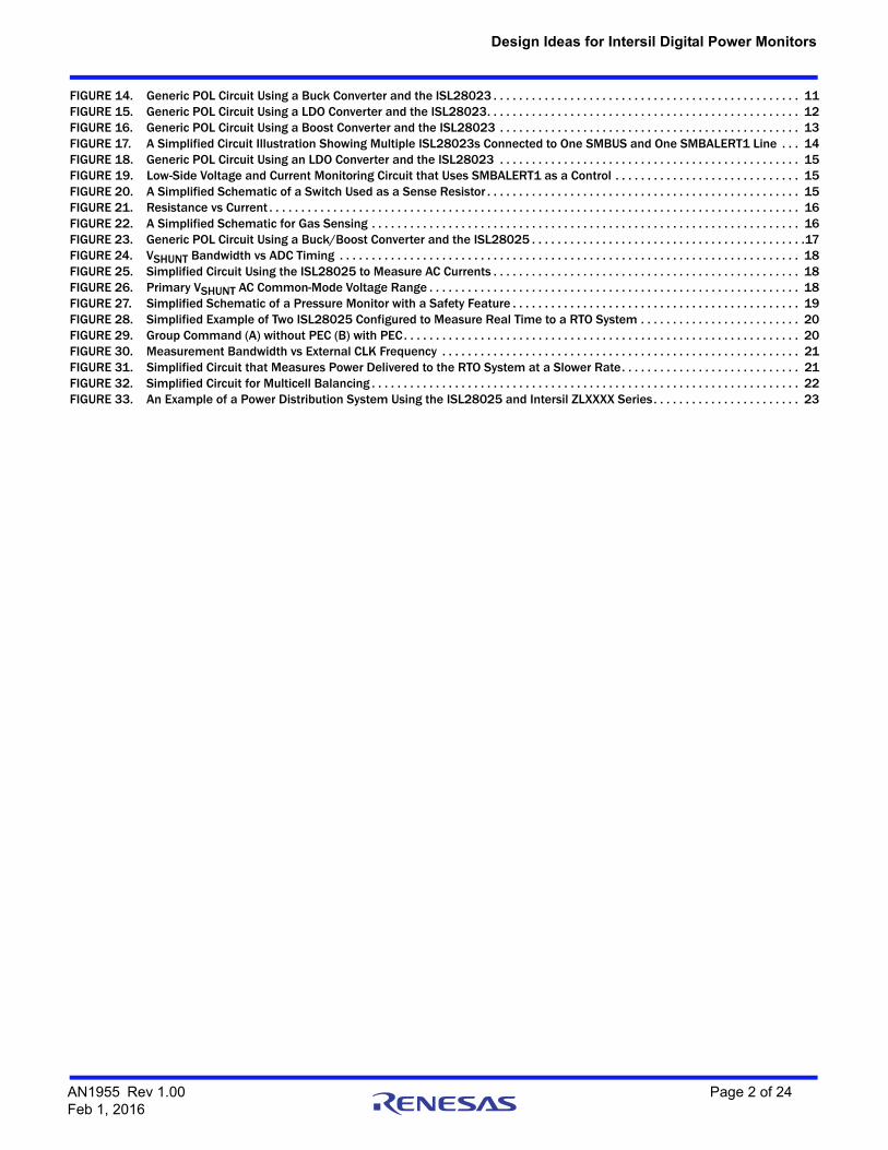
Ideas Using ISL28022Point-of-Load Power MonitorThe circuit illustrated in Figure 1 is a solution that can be used to monitor a load’s performance. The voltage regulator regulates to a Point-of-Load (POL) voltage. 5V, 3.3V, 2.5V and 1.8V are examples of POL voltages.
The main bus voltage applied to the voltage regulator regulates the voltage to the load at the VINM, VBUS and Sense node for the configuration shown in Figure 1. The shunt resistor in the circuit allows the current to be monitored while regulating the voltage to the load. For example, the maximum shunt voltage the ISL28022 is able to measure is ±320mV. The shunt resistor value is determined by Equation 1:
CurrentFS is the maximum current to be measured through the load. This is chosen by the user.
The DPM has Overvoltage/Undervoltage (OV/UV) sensing circuitry for the Bus and Shunt inputs. The levels of the error detection circuitry are controlled digitally via an I2C/SMBus interface. The status of each inputs’ error detection can be read digitally via a register. The DPM allows for the summation of error detection bits to be routed to an interrupt pin. For the point-of-load monitoring circuit shown in Figure 1, the interrupt pin is connected to the enable pin of the regulator. In a fault condition, the DPM will trigger an interrupt causing the voltage regulator to shut down. When a fault exists, the DPM interrupt pin output state can be digitally programmed.
The DPM calculates the power and current internally and stores the results in an internal register. The VBUS connected directly to the load, enables a measurement system that monitors power to the load.
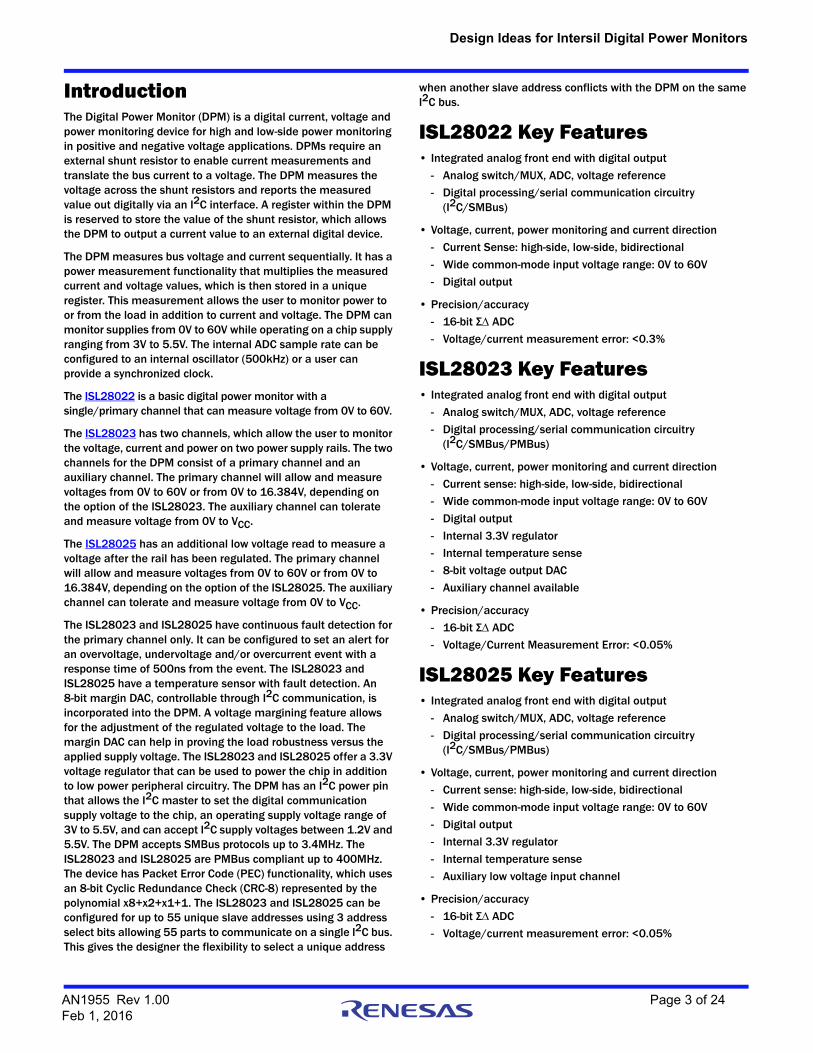
Adjustable Point-of-Load Monitor Many applications require unique voltages to optimize a circuit’s potential. Figure 2 is a microcontroller selectable Point-of-Load (POL) circuit. The circuit is very similar to the POL monitor discussed previously. The General Purpose Input Output (GPIO) bits of the microcontroller controls a multiplexer, which connects a gain setting resistor to the adjust (ADJ) pin of the regulator. The feedback resistance (RF), the multiplexer switch resistance and the value of the gain setting resistor (R1 to R8) determine the regulated output voltage (POL_V) to the load. Equation 2 is a generic formula to determine the regulated POL_V.
The coefficient alpha, , is dependent on the designed in regulator. For the ISL80101-ADJ, equals 0.5. Rx is the value of the gain resistor (R1 to R8) selected by the microcontroller. Rmux is the multiplexer switch resistor value. The multiplexer switch resistance is a function of the current flowing through the switch. A general practice is to choose resistor values such that current flowing through the multiplexer is small. The ISL84781 has an ON-resistance of 0.4Ω
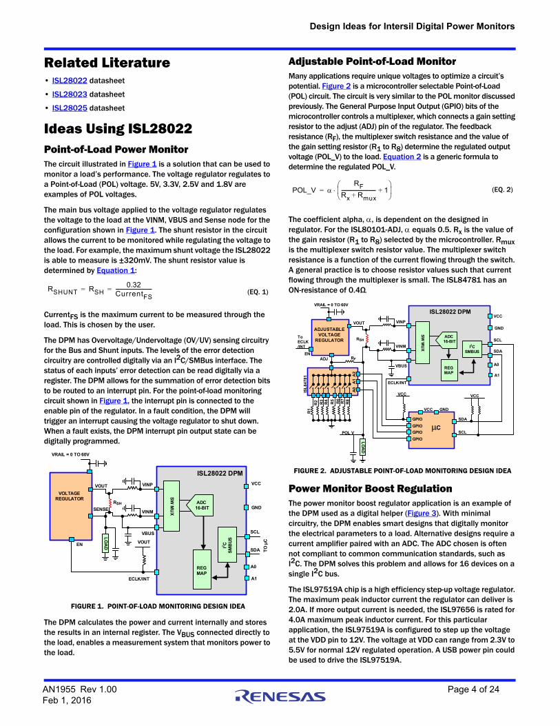
Power Monitor Boost RegulationThe power monitor boost regulator application is an example of the DPM used as a digital helper (Figure 3). With minimal circuitry, the DPM enables smart designs that digitally monitor the electrical parameters to a load. Alternative designs require a current amplifier paired with an ADC. The ADC chosen is often not compliant to common communication standards, such as I2C. The DPM solves this problem and allows for 16 devices on a single I2C bus.
The ISL97519A chip is a high efficiency step-up voltage regulator. The maximum peak inductor current the regulator can deliver is 2.0A. If more output current is needed, the ISL97656 is rated for 4.0A maximum peak inductor current. For this particular application, the ISL97519A is configured to step up the voltage at the VDD pin to 12V. The voltage at VDD can range from 2.3V to 5.5V for normal 12V regulated operation. A USB power pin could be used to drive the ISL97519A.
(EQ. 1)RSHUNT RSH0.32
CurrentFS------------------------------= =
FIGURE 1. POINT-OF-LOAD MONITORING DESIGN IDEA
I2 CSM
BUS
A1
SCL
SDA
VINP
VINMGND
RSH ADC 16-BIT
SW M
UX
VOUT
EN
ECLK/INT
VRAIL = 0 TO 60V
REG MAP
VCC
VBUS
A0
ISL28022 DPM
SENSE
VOUT
VOLTAGE REGULATOR
LOA
D
TO µ
C
FIGURE 2. ADJUSTABLE POINT-OF-LOAD MONITORING DESIGN IDEA
(EQ. 2)POL_V RF
Rx Rmux+---------------------------- 1+ =
I2CSMBUS
A1
SCL
SDA
VINP
VINM
GND
RSHADC
16-BIT
SW M
UX
VOUT
EN
VRAIL = 0 TO 60V
REG MAP
VCC
VBUS A0
ISL28022 DPM
ADJ
ADJUSTABLEVOLTAGE
REGULATOR
LOA
D
ISL8
4781
A0A1
A2
R1R2 R3 R4 R5 R6 R7 R8
C
RF
SCL
SDA
VCC
GNDVCC
ECLK/INT
GPIOGPIOGPIOGPIO
POL V
To ECLK/INT
VCC
�
AN1955 Rev 1.00 Page 4 of 24Feb 1, 2016
Design Ideas for Intersil Digital Power Monitors
The regulation node of the circuit, shown in Figure 3 is at VOUT. The ISL97519A has feedback circuitry that removes the current sense resistor, RSH, from impacting the regulation voltage. Equation 1 on page 4 shows the formula used to calculate RSHUNT.
The DPM interrupt pin is connected to the Enable pin of the regulator. The DPM has OV/UV alerts for both the Bus and Shunt channels. A fault condition from either channel powers down the voltage regulator.
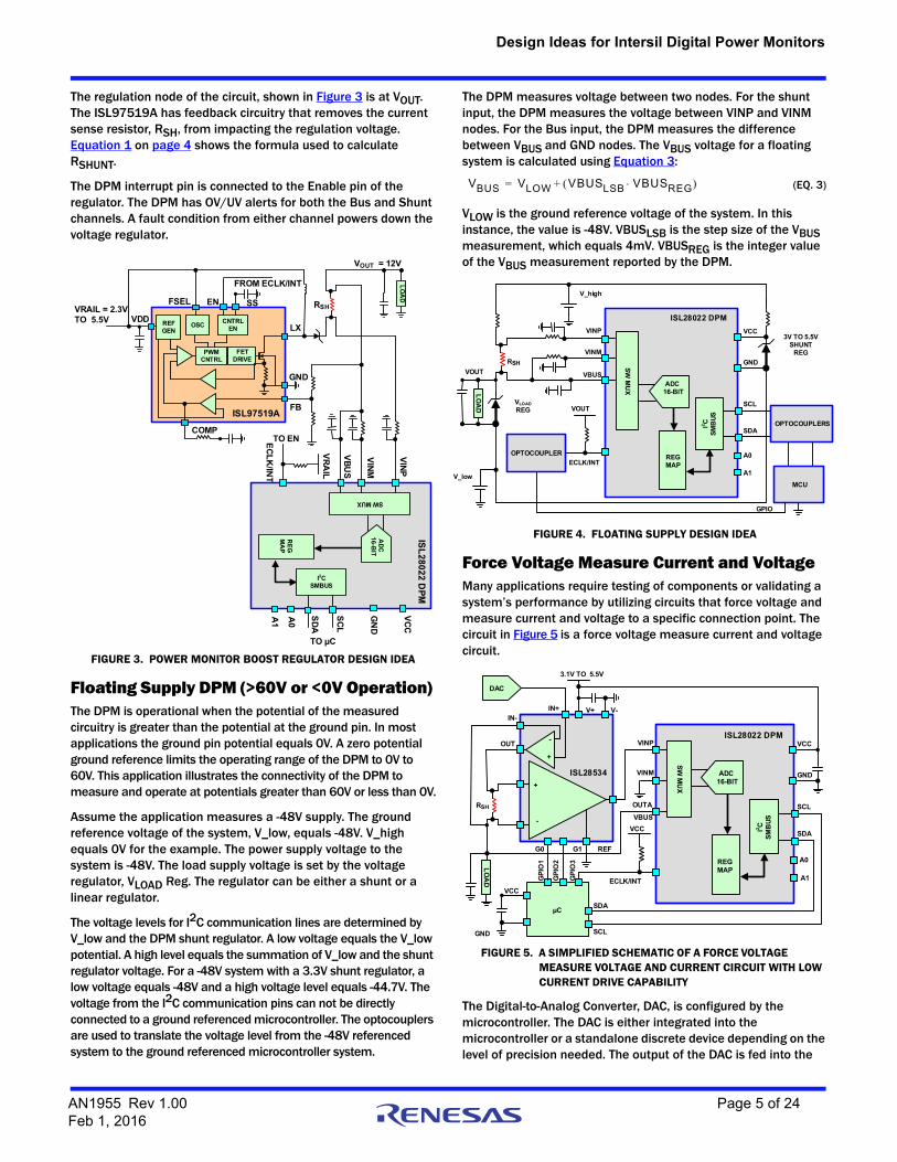
Floating Supply DPM (>60V or <0V Operation) The DPM is operational when the potential of the measured circuitry is greater than the potential at the ground pin. In most applications the ground pin potential equals 0V. A zero potential ground reference limits the operating range of the DPM to 0V to 60V. This application illustrates the connectivity of the DPM to measure and operate at potentials greater than 60V or less than 0V.
Assume the application measures a -48V supply. The ground reference voltage of the system, V_low, equals -48V. V_high equals 0V for the example. The power supply voltage to the system is -48V. The load supply voltage is set by the voltage regulator, VLOAD Reg. The regulator can be either a shunt or a linear regulator.
The voltage levels for I2C communication lines are determined by V_low and the DPM shunt regulator. A low voltage equals the V_low potential. A high level equals the summation of V_low and the shunt regulator voltage. For a -48V system with a 3.3V shunt regulator, a low voltage equals -48V and a high voltage level equals -44.7V. The voltage from the I2C communication pins can not be directly connected to a ground referenced microcontroller. The optocouplers are used to translate the voltage level from the -48V referenced system to the ground referenced microcontroller system.
The DPM measures voltage between two nodes. For the shunt input, the DPM measures the voltage between VINP and VINM nodes. For the Bus input, the DPM measures the difference between VBUS and GND nodes. The VBUS voltage for a floating system is calculated using Equation 3:
VLOW is the ground reference voltage of the system. In this instance, the value is -48V. VBUSLSB is the step size of the VBUS measurement, which equals 4mV. VBUSREG is the integer value of the VBUS measurement reported by the DPM.
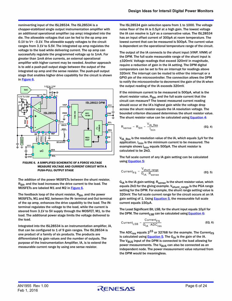
Force Voltage Measure Current and VoltageMany applications require testing of components or validating a system’s performance by utilizing circuits that force voltage and measure current and voltage to a specific connection point. The circuit in Figure 5 is a force voltage measure current and voltage circuit.
The Digital-to-Analog Converter, DAC, is configured by the microcontroller. The DAC is either integrated into the microcontroller or a standalone discrete device depending on the level of precision needed. The output of the DAC is fed into the
FIGURE 3. POWER MONITOR BOOST REGULATOR DESIGN IDEA
RSH
VOUT = 12V
VRAIL = 2.3V TO 5.5V
LOA
D
REFGEN
OSC CNTRL EN
PWMCNTRL
FETDRIVE
ISL97519ACOMP
VDD
FB
GND
LX
SSENFSEL
FROM ECLK/INT
I2CSMBUS
A1
SCL
SDA
VINP
VINMG
ND
ADC
16-BIT
ECLK/IN
T
REG
M
AP
VCC
VBUS
A0
ISL28022 DPM
VRAIL
TO µCSW MUX
TO EN
FIGURE 4. FLOATING SUPPLY DESIGN IDEA
FIGURE 5. A SIMPLIFIED SCHEMATIC OF A FORCE VOLTAGE MEASURE VOLTAGE AND CURRENT CIRCUIT WITH LOW CURRENT DRIVE CAPABILITY
(EQ. 3)VBUS VLOW VBUSLSB VBUSREG +=
I2 CSM
BUS
A1
SCL
SDA
VINP
VINMGNDRSH
ADC 16-BIT
SW M
UX
VOUT
ECLK/INTREG MAP
VCC
VBUS
A0
ISL28022 DPM
VOUT
3V TO 5.5VSHUNT
REG
OPTOCOUPLERS
V_low
VLOADREG
MCU
V_high
LOA
D
OPTOCOUPLER
GPIO
I2 CSM
BUS
A1
SCL
SDA
VINP
VINM GND
RSH
ADC 16-BIT
SW M
UX
ECLK/INT
REG MAP
VBUS
A0
ISL28022 DPM
VCC
OUTA
OUT
G0 G1 REF
+
-
V-V+
ISL28534
GPI
O1
GPI
O2
SDA
SCL
µC
+
-
3.1V TO 5.5V
IN-IN+
GPI
O3
VCC
VCC
GND
LOA
D
DAC
AN1955 Rev 1.00 Page 5 of 24Feb 1, 2016
Design Ideas for Intersil Digital Power Monitors
noninverting input of the ISL28534. The ISL28534 is a chopper-stabilized single output instrumentation amplifier with an additional operational amplifier (op amp) integrated into the die. The allowable voltages that can be fed to the op amp are 0.1V to V+ - 0.1V. The allowable supply voltages to the circuit ranges from 3.1V to 5.5V. The integrated op amp regulates the voltage to the load while delivering current. The op amp can successfully regulate the programmed voltage up to 1mA. For greater than 1mA drive currents, an external operational amplifier with higher current may be needed. Another approach is to add a push-pull output stage between the output of the integrated op amp and the sense resistor. The push-pull output stage that enables higher drive capability for the circuit is shown in Figure 6.
The addition of the power MOSFETs between the shunt resistor, RSH, and the load increases the drive current to the load. The MOSFETs are labeled M1 and M2 in Figure 6.
The feedback loop of the shunt resistor, RSH, and the power MOSFETs, M1 and M2, between the IN- terminal and Out terminal of the op amp, enhances the drive capability to the load. The IN- terminal regulates the voltage to the load, while the current is steered from 3.1V to 5V supply through the MOSFET, M1, to the load. The additional power stage limits the voltage delivered to the load.
Integrated into the ISL28534 is an instrumentation amplifier, IA, that can be configured to 1 of 9 gain ranges. The ISL28534 is one product of a family of six products. The products are differentiated by gain values and the number of outputs. The purpose of the Instrumentation Amplifier, IA, is to extend the measurable current range by using one sense resistor.
The ISL28534 gain selection spans from 1 to 1000. The voltage noise floor of the IA is 0.5µV at a high gain. The lowest voltage the IA can resolve is 1µV as a conservative value. The ISL28534 has an input offset current of 300pA at room temperature. The lowest current that can be measured is 500pA. The current value is dependent on the operational temperature range of the circuit.
The output of the IA connects to the shunt input (VINP, VINM) of the DPM. The full scale measurable range of the shunt input is ±320mV. Voltage readings that exceed 320mV in magnitude, require a reduction of gain in the IA setting. The DPM digital comparators can be set to fire an interrupt for readings above 320mV. The interrupt can be routed to either the interrupt or a GPIO pin of the microcontroller. The connection allows the DPM to notify the microcontroller to decrement the gain of the IA when the output reading of the IA exceeds 320mV.
If the minimum current to be measured is 500pA, what is the shunt resistor value, RSH, and the full scale current that the circuit can measure? The lowest measured current reading should occur at the IA’s highest gain while the voltage drop across the shunt resistor equals the IA resolution voltage. The bounded criterion discussed determines the shunt resistor value. The shunt resistor value can be calculated using Equation 4:
VIA_Res is the resolution value of the IA, which equals 1µV for the application. Imin is the minimum current to be measured. The example shows Imin equals 500pA. The shunt resistor is calculated to be 2kΩ.
The full scale current of any IA gain setting can be calculated using Equation 5:
GIA is the IA gain setting. Rsense is the shunt resistor value, which equals 2kΩ for the giving example. Vshunt_range is the PGA range setting for the DPM. For example, the shunt range setting value is 320mV. The full scale current range for the circuit occurs at an IA gain setting of 1. Using Equation 5, the measurable full scale current equals 150µA.
The Least Significant Bit, LSB, for the shunt input equals 10µV for the DPM. The currentLSB can be calculated using Equation 6:
The ADCres equals 215 or 32768 for the example. The CurrentFSis calculated using Equation 5. The GIA is the gain of the IA.The VBUS input of the DPM is connected to the load allowing for power measurements. The VBUS can also be connected as an independent node. The power measurement value returned from the DPM would be meaningless.
FIGURE 6. A SIMPLIFIED SCHEMATIC OF A FORCE VOLTAGE MEASURE VOLTAGE AND CURRENT CIRCUIT WITH A PUSH-PULL OUTPUT STAGE
(EQ. 4)Rsense RSH
VIA_ResImin
---------------------= =
(EQ. 5)CurrentFS
Vshunt_rangeGIA Rsense----------------------------------=
(EQ. 6)CurrentLSB
CurrentFSGIA ADCres------------------------------------=
AN1955 Rev 1.00 Page 6 of 24Feb 1, 2016
Design Ideas for Intersil Digital Power Monitors
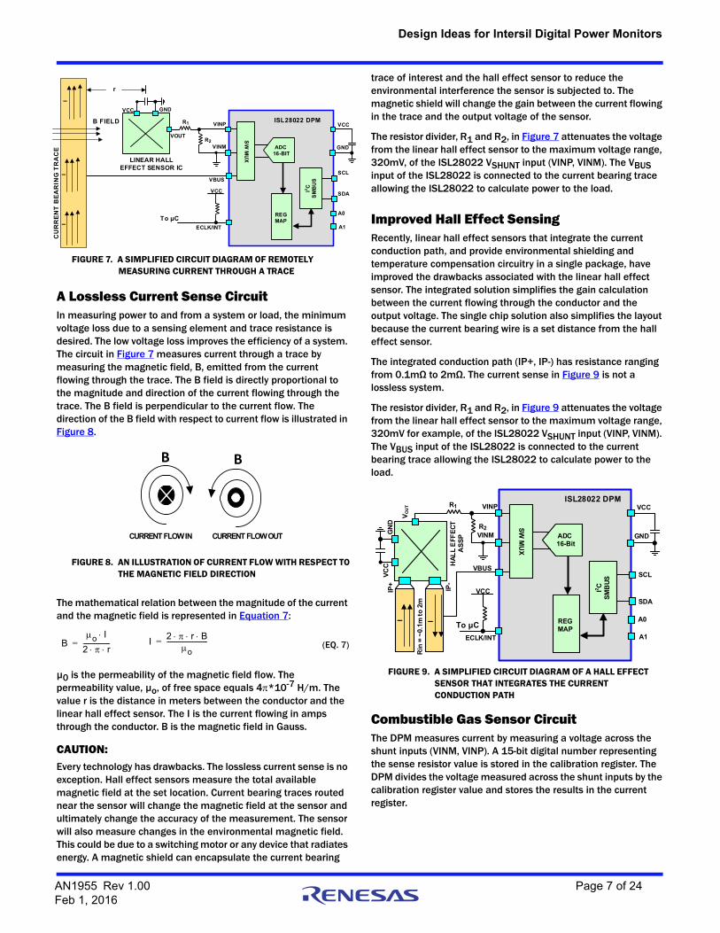
A Lossless Current Sense CircuitIn measuring power to and from a system or load, the minimum voltage loss due to a sensing element and trace resistance is desired. The low voltage loss improves the efficiency of a system. The circuit in Figure 7 measures current through a trace by measuring the magnetic field, B, emitted from the current flowing through the trace. The B field is directly proportional to the magnitude and direction of the current flowing through the trace. The B field is perpendicular to the current flow. The direction of the B field with respect to current flow is illustrated in Figure 8.
The mathematical relation between the magnitude of the current and the magnetic field is represented in Equation 7:
µ0 is the permeability of the magnetic field flow. The permeability value, µo, of free space equals 4*10-7 H/m. The value r is the distance in meters between the conductor and the linear hall effect sensor. The I is the current flowing in amps through the conductor. B is the magnetic field in Gauss.
CAUTION:Every technology has drawbacks. The lossless current sense is no exception. Hall effect sensors measure the total available magnetic field at the set location. Current bearing traces routed near the sensor will change the magnetic field at the sensor and ultimately change the accuracy of the measurement. The sensor will also measure changes in the environmental magnetic field. This could be due to a switching motor or any device that radiates energy. A magnetic shield can encapsulate the current bearing
trace of interest and the hall effect sensor to reduce the environmental interference the sensor is subjected to. The magnetic shield will change the gain between the current flowing in the trace and the output voltage of the sensor.
The resistor divider, R1 and R2, in Figure 7 attenuates the voltage from the linear hall effect sensor to the maximum voltage range, 320mV, of the ISL28022 VSHUNT input (VINP, VINM). The VBUS input of the ISL28022 is connected to the current bearing trace allowing the ISL28022 to calculate power to the load.
Improved Hall Effect SensingRecently, linear hall effect sensors that integrate the current conduction path, and provide environmental shielding and temperature compensation circuitry in a single package, have improved the drawbacks associated with the linear hall effect sensor. The integrated solution simplifies the gain calculation between the current flowing through the conductor and the output voltage. The single chip solution also simplifies the layout because the current bearing wire is a set distance from the hall effect sensor.
The integrated conduction path (IP+, IP-) has resistance ranging from 0.1mΩ to 2mΩ. The current sense in Figure 9 is not a lossless system.
The resistor divider, R1 and R2, in Figure 9 attenuates the voltage from the linear hall effect sensor to the maximum voltage range, 320mV for example, of the ISL28022 VSHUNT input (VINP, VINM). The VBUS input of the ISL28022 is connected to the current bearing trace allowing the ISL28022 to calculate power to the load.
Combustible Gas Sensor CircuitThe DPM measures current by measuring a voltage across the shunt inputs (VINM, VINP). A 15-bit digital number representing the sense resistor value is stored in the calibration register. The DPM divides the voltage measured across the shunt inputs by the calibration register value and stores the results in the current register.
FIGURE 7. A SIMPLIFIED CIRCUIT DIAGRAM OF REMOTELY MEASURING CURRENT THROUGH A TRACE
FIGURE 8. AN ILLUSTRATION OF CURRENT FLOW WITH RESPECT TO THE MAGNETIC FIELD DIRECTION
I2 CS
MB
US
A1
SCL
SDA
VINP
VINM GNDADC 16-BIT
SW
MU
X
ECLK/INT
REG MAP
VBUS
A0
ISL28022 DPM
VCC
VCCR1
R2VOUT
LINEAR HALL EFFECT SENSOR IC
VCC GND
CU
RR
ENT
BEA
RIN
G T
RA
CE
B FIELD
II
I
r
To µC
B B
CURRENT FLOW OUTCURRENT FLOW IN
(EQ. 7)I2 r B
o--------------------------=B
o I
2 r -----------------=
FIGURE 9. A SIMPLIFIED CIRCUIT DIAGRAM OF A HALL EFFECT SENSOR THAT INTEGRATES THE CURRENT CONDUCTION PATH
I2 CSM
BUS
A1
SCL
SDA
VINP
VINM GNDADC 16-Bit
SW M
UX
ECLK/INT
REG MAP
VBUS
A0
ISL28022 DPM
VCC
VCCR1
R2
V OUT
HAL
L E
FFEC
T A
SSP
VCC
GN
DI
To µC
I
IP+ IP-
Rin
= ~
0.1m
to 2
m
AN1955 Rev 1.00 Page 7 of 24Feb 1, 2016
Design Ideas for Intersil Digital Power Monitors
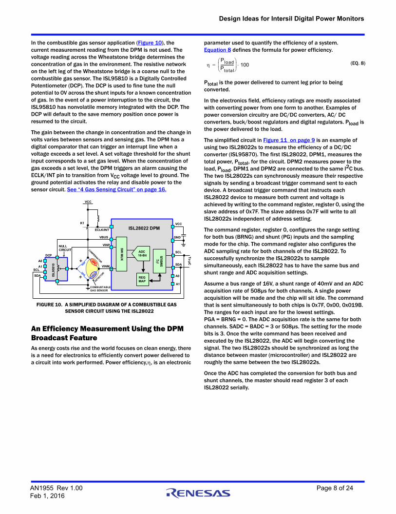
In the combustible gas sensor application (Figure 10), the current measurement reading from the DPM is not used. The voltage reading across the Wheatstone bridge determines the concentration of gas in the environment. The resistive network on the left leg of the Wheatstone bridge is a coarse null to the combustible gas sensor. The ISL95810 is a Digitally Controlled Potentiometer (DCP). The DCP is used to fine tune the null potential to 0V across the shunt inputs for a known concentration of gas. In the event of a power interruption to the circuit, the ISL95810 has nonvolatile memory integrated with the DCP. The DCP will default to the save memory position once power is resumed to the circuit.
The gain between the change in concentration and the change in volts varies between sensors and sensing gas. The DPM has a digital comparator that can trigger an interrupt line when a voltage exceeds a set level. A set voltage threshold for the shunt input corresponds to a set gas level. When the concentration of gas exceeds a set level, the DPM triggers an alarm causing the ECLK/INT pin to transition from VCC voltage level to ground. The ground potential activates the relay and disable power to the sensor circuit. See “4 Gas Sensing Circuit” on page 16.
An Efficiency Measurement Using the DPM Broadcast FeatureAs energy costs rise and the world focuses on clean energy, there is a need for electronics to efficiently convert power delivered to a circuit into work performed. Power efficiency,, is an electronic
parameter used to quantify the efficiency of a system. Equation 8 defines the formula for power efficiency.
Ptotal is the power delivered to current leg prior to being converted.
In the electronics field, efficiency ratings are mostly associated with converting power from one form to another. Examples of power conversion circuitry are DC/DC converters, AC/ DC converters, buck/boost regulators and digital regulators. Pload is the power delivered to the load.
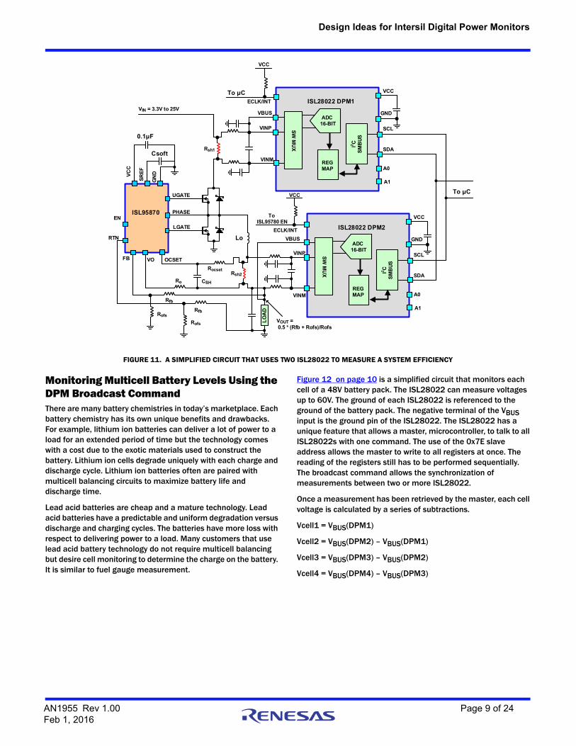
The simplified circuit in Figure 11 on page 9 is an example of using two ISL28022s to measure the efficiency of a DC/DC converter (ISL95870). The first ISL28022, DPM1, measures the total power, Ptotal, for the circuit. DPM2 measures power to the load, Pload. DPM1 and DPM2 are connected to the same I2C bus. The two ISL28022s can synchronously measure their respective signals by sending a broadcast trigger command sent to each device. A broadcast trigger command that instructs each ISL28022 device to measure both current and voltage is achieved by writing to the command register, register 0, using the slave address of 0x7F. The slave address 0x7F will write to all ISL28022s independent of address setting.
The command register, register 0, configures the range setting for both bus (BRNG) and shunt (PG) inputs and the sampling mode for the chip. The command register also configures the ADC sampling rate for both channels of the ISL28022. To successfully synchronize the ISL28022s to sample simultaneously, each ISL28022 has to have the same bus and shunt range and ADC acquisition settings.
Assume a bus range of 16V, a shunt range of 40mV and an ADC acquisition rate of 508µs for both channels. A single power acquisition will be made and the chip will sit idle. The command that is sent simultaneously to both chips is 0x7F, 0x00, 0x019B. The ranges for each input are for the lowest settings. PGA = BRNG = 0. The ADC acquisition rate is the same for both channels. SADC = BADC = 3 or 508µs. The setting for the mode bits is 3. Once the write command has been received and executed by the ISL28022, the ADC will begin converting the signal. The two ISL28022s should be synchronized as long the distance between master (microcontroller) and ISL28022 are roughly the same between the two ISL28022s.
Once the ADC has completed the conversion for both bus and shunt channels, the master should read register 3 of each ISL28022 serially.
I2 CSM
BUS
A1
SCL
SDA
VINP
VINM
GND
ADC 16-Bit
SW M
UX
ECLK/INT
REG MAP
VBUS
A0
ISL28022 DPM
VCC
VCC
To µC
ISL9
5810
A0A1
SDA
SCL
DCP
COMBUSTABLE GAS SENSOR
NULL CIRCUIT
K1
FIGURE 10. A SIMPLIFIED DIAGRAM OF A COMBUSTIBLE GAS SENSOR CIRCUIT USING THE ISL28022
(EQ. 8)PloadPtotal---------------
100=
AN1955 Rev 1.00 Page 8 of 24Feb 1, 2016
Design Ideas for Intersil Digital Power Monitors
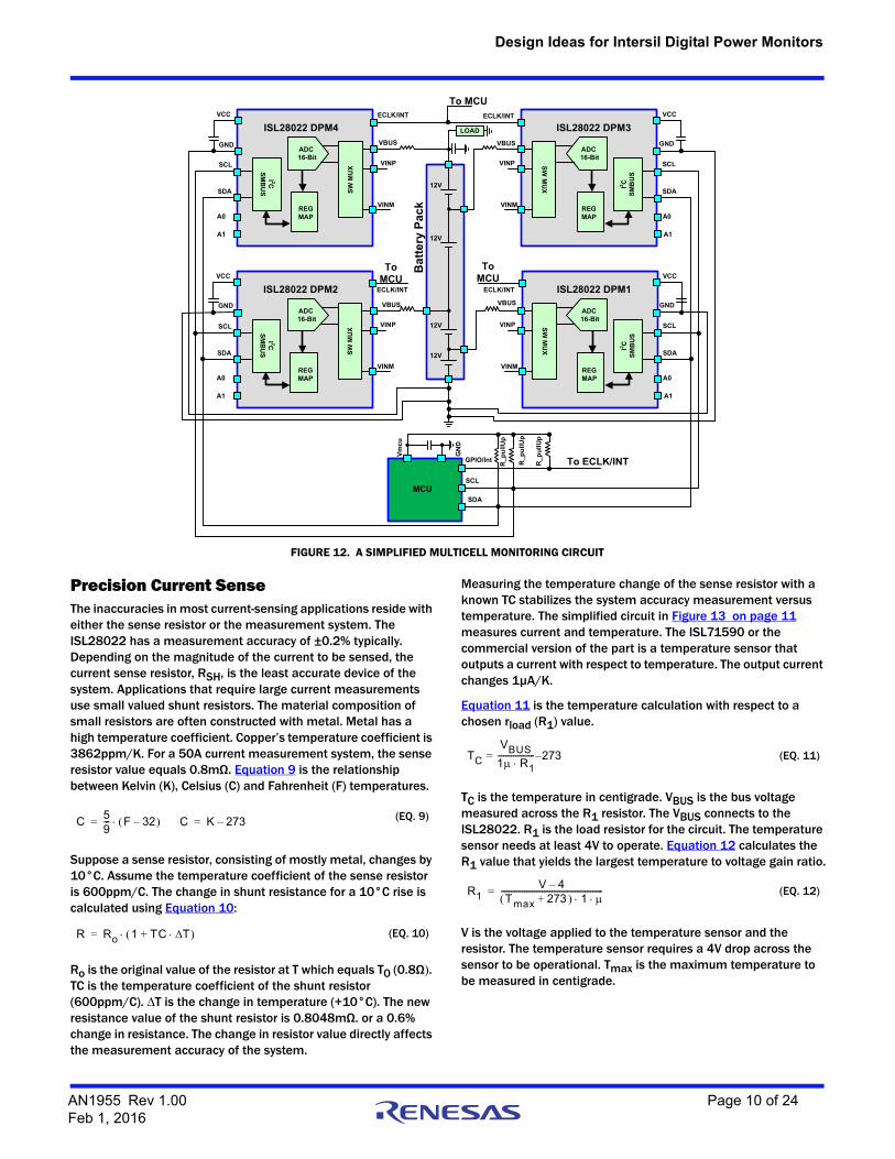
Monitoring Multicell Battery Levels Using the DPM Broadcast CommandThere are many battery chemistries in today’s marketplace. Each battery chemistry has its own unique benefits and drawbacks. For example, lithium ion batteries can deliver a lot of power to a load for an extended period of time but the technology comes with a cost due to the exotic materials used to construct the battery. Lithium ion cells degrade uniquely with each charge and discharge cycle. Lithium ion batteries often are paired with multicell balancing circuits to maximize battery life and discharge time.
Lead acid batteries are cheap and a mature technology. Lead acid batteries have a predictable and uniform degradation versus discharge and charging cycles. The batteries have more loss with respect to delivering power to a load. Many customers that use lead acid battery technology do not require multicell balancing but desire cell monitoring to determine the charge on the battery. It is similar to fuel gauge measurement.
Figure 12 on page 10 is a simplified circuit that monitors each cell of a 48V battery pack. The ISL28022 can measure voltages up to 60V. The ground of each ISL28022 is referenced to the ground of the battery pack. The negative terminal of the VBUS input is the ground pin of the ISL28022. The ISL28022 has a unique feature that allows a master, microcontroller, to talk to all ISL28022s with one command. The use of the 0x7E slave address allows the master to write to all registers at once. The reading of the registers still has to be performed sequentially. The broadcast command allows the synchronization of measurements between two or more ISL28022.
Once a measurement has been retrieved by the master, each cell voltage is calculated by a series of subtractions.
Vcell1 = VBUS(DPM1)
Vcell2 = VBUS(DPM2) – VBUS(DPM1)
Vcell3 = VBUS(DPM3) – VBUS(DPM2)
Vcell4 = VBUS(DPM4) – VBUS(DPM3)
FIGURE 11. A SIMPLIFIED CIRCUIT THAT USES TWO ISL28022 TO MEASURE A SYSTEM EFFICIENCY
Rsh1
LOA
DFB
ISL95870
VOUT = 0.5 * (Rfb + Rofs)/Rofs
VIN = 3.3V to 25V
LGATE
UGATE
PHASE
OCSET
Ro
VORocset
Rfb
CSH
Rsh2
Lo
Rofs
RTN
Rfb
Rofs
VCC
GN
D
SREF
Csoft
0.1µF
ECLK/INTTo µC
VCC
I2 CSM
BUS
A1
SCL
SDA
VINP
GNDADC
16-BITSW
MU
X
REG MAP A0
ISL28022 DPM2VCCTo
ISL95780 EN
VINM
VBUS
VCC
ECLK/INT
I2 CSM
BUS
A1
SCL
SDA
VINP
GNDADC
16-BIT
SW M
UX
REG MAP A0
ISL28022 DPM1VCC
VINM
VBUS
To µC
EN
AN1955 Rev 1.00 Page 9 of 24Feb 1, 2016
Design Ideas for Intersil Digital Power Monitors
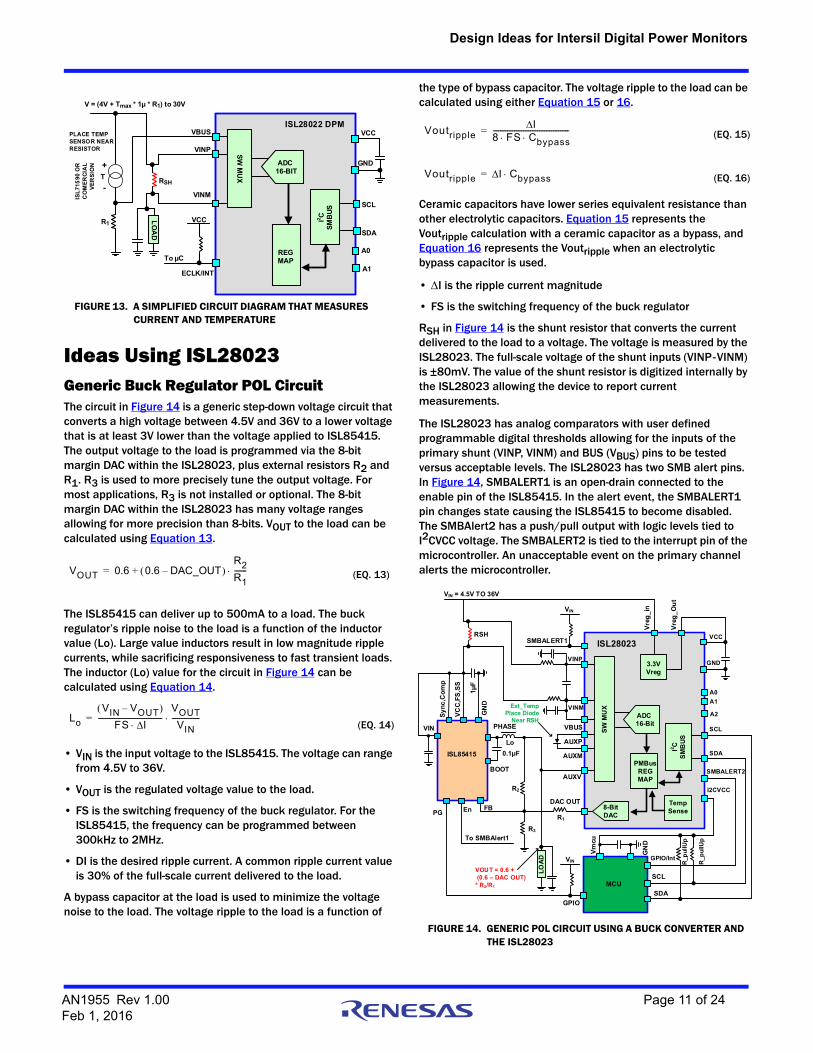
Precision Current SenseThe inaccuracies in most current-sensing applications reside with either the sense resistor or the measurement system. The ISL28022 has a measurement accuracy of ±0.2% typically. Depending on the magnitude of the current to be sensed, the current sense resistor, RSH, is the least accurate device of the system. Applications that require large current measurements use small valued shunt resistors. The material composition of small resistors are often constructed with metal. Metal has a high temperature coefficient. Copper’s temperature coefficient is 3862ppm/K. For a 50A current measurement system, the sense resistor value equals 0.8mΩ. Equation 9 is the relationship between Kelvin (K), Celsius (C) and Fahrenheit (F) temperatures.
Suppose a sense resistor, consisting of mostly metal, changes by 10°C. Assume the temperature coefficient of the sense resistor is 600ppm/C. The change in shunt resistance for a 10°C rise is calculated using Equation 10:
Ro is the original value of the resistor at T which equals T0 (0.8Ω. TC is the temperature coefficient of the shunt resistor (600ppm/C). T is the change in temperature (+10°C). The new resistance value of the shunt resistor is 0.8048mΩ. or a 0.6% change in resistance. The change in resistor value directly affects the measurement accuracy of the system.
Measuring the temperature change of the sense resistor with a known TC stabilizes the system accuracy measurement versus temperature. The simplified circuit in Figure 13 on page 11 measures current and temperature. The ISL71590 or the commercial version of the part is a temperature sensor that outputs a current with respect to temperature. The output current changes 1µA/K.
Equation 11 is the temperature calculation with respect to a chosen rload (R1) value.
TC is the temperature in centigrade. VBUS is the bus voltage measured across the R1 resistor. The VBUS connects to the ISL28022. R1 is the load resistor for the circuit. The temperature sensor needs at least 4V to operate. Equation 12 calculates the R1 value that yields the largest temperature to voltage gain ratio.
V is the voltage applied to the temperature sensor and the resistor. The temperature sensor requires a 4V drop across the sensor to be operational. Tmax is the maximum temperature to be measured in centigrade.
FIGURE 12. A SIMPLIFIED MULTICELL MONITORING CIRCUIT
ECLK/INT
I2 CS
MB
US
A1
SCL
SDA
VINP
GNDADC
16-Bit
SW
MU
X
REG MAP A0
ISL28022 DPM3
VCC
VINM
VBUS
ECLK/INT
I2C
SM
BU
S
A1
SCL
SDA
VINP
GNDADC
16-Bit
SW
MU
X
REG MAP A0
ISL28022 DPM1
VCC
VINM
VBUS
ECLK/INT
To MCU
I 2CS
MB
US
A1
SCL
SDA
VINP
GNDADC
16-Bit
SW
MU
X
REG MAPA0
ISL28022 DPM4
VCC
VINM
VBUS
ECLK/INT
I 2CS
MB
US
A1
SCL
SDA
VINP
GNDADC
16-Bit
SW
MU
X
REG MAPA0
ISL28022 DPM2
VCC
VINM
VBUS
12V
12V
12V
12V
Ba
tte
ry P
ack
To MCU
To MCU
Vm
cu
GN
DGPIO/Int
SDA
SCL
R_
pu
llU
p
R_
pu
llUp
MCU
R_
pu
llU
p
To ECLK/INT
LOAD
(EQ. 9)C59--- F 32– = C K 273–=
(EQ. 10)R Ro 1 TC T+ =
(EQ. 11)TC
VBUS1 R1-------------------= 273–
(EQ. 12)R1V 4–
T max 273 1 +----------------------------------------------------=
AN1955 Rev 1.00 Page 10 of 24Feb 1, 2016
Design Ideas for Intersil Digital Power Monitors
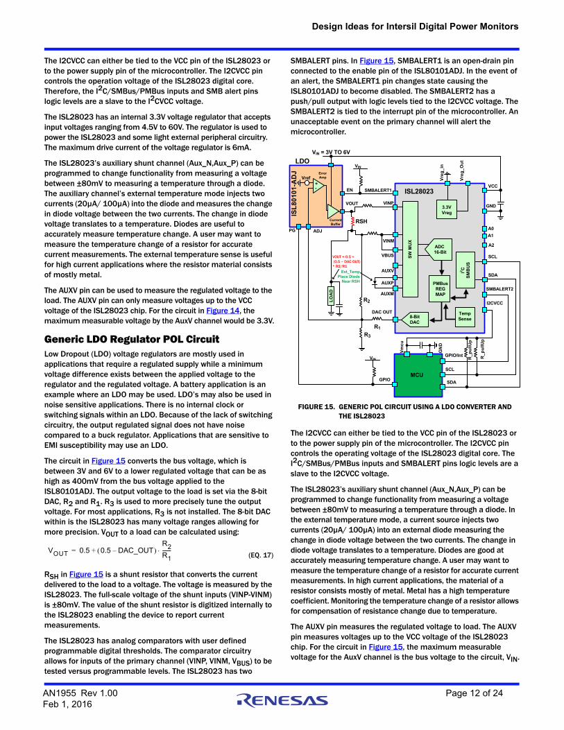
Ideas Using ISL28023Generic Buck Regulator POL CircuitThe circuit in Figure 14 is a generic step-down voltage circuit that converts a high voltage between 4.5V and 36V to a lower voltage that is at least 3V lower than the voltage applied to ISL85415. The output voltage to the load is programmed via the 8-bit margin DAC within the ISL28023, plus external resistors R2 and R1. R3 is used to more precisely tune the output voltage. For most applications, R3 is not installed or optional. The 8-bit margin DAC within the ISL28023 has many voltage ranges allowing for more precision than 8-bits. VOUT to the load can be calculated using Equation 13.
The ISL85415 can deliver up to 500mA to a load. The buck regulator’s ripple noise to the load is a function of the inductor value (Lo). Large value inductors result in low magnitude ripple currents, while sacrificing responsiveness to fast transient loads. The inductor (Lo) value for the circuit in Figure 14 can be calculated using Equation 14.
• VIN is the input voltage to the ISL85415. The voltage can range from 4.5V to 36V.
• VOUT is the regulated voltage value to the load.
• FS is the switching frequency of the buck regulator. For the ISL85415, the frequency can be programmed between 300kHz to 2MHz.
• DI is the desired ripple current. A common ripple current value is 30% of the full-scale current delivered to the load.
A bypass capacitor at the load is used to minimize the voltage noise to the load. The voltage ripple to the load is a function of
the type of bypass capacitor. The voltage ripple to the load can be calculated using either Equation 15 or 16.
Ceramic capacitors have lower series equivalent resistance than other electrolytic capacitors. Equation 15 represents the Voutripple calculation with a ceramic capacitor as a bypass, and Equation 16 represents the Voutripple when an electrolytic bypass capacitor is used.
• I is the ripple current magnitude
• FS is the switching frequency of the buck regulator
RSH in Figure 14 is the shunt resistor that converts the current delivered to the load to a voltage. The voltage is measured by the ISL28023. The full-scale voltage of the shunt inputs (VINP-VINM) is ±80mV. The value of the shunt resistor is digitized internally by the ISL28023 allowing the device to report current measurements.
The ISL28023 has analog comparators with user defined programmable digital thresholds allowing for the inputs of the primary shunt (VINP, VINM) and BUS (VBUS) pins to be tested versus acceptable levels. The ISL28023 has two SMB alert pins. In Figure 14, SMBALERT1 is an open-drain connected to the enable pin of the ISL85415. In the alert event, the SMBALERT1 pin changes state causing the ISL85415 to become disabled. The SMBAlert2 has a push/pull output with logic levels tied to I2CVCC voltage. The SMBALERT2 is tied to the interrupt pin of the microcontroller. An unacceptable event on the primary channel alerts the microcontroller.
FIGURE 13. A SIMPLIFIED CIRCUIT DIAGRAM THAT MEASURES CURRENT AND TEMPERATURE
I2 CSM
BUS
A1
SCL
SDA
VINP
VINM
GNDADC 16-BIT
SW M
UX
ECLK/INT
REG MAP
VBUS
A0
ISL28022 DPM
VCC
VCC
RSH
LOA
D
PLACE TEMP SENSOR NEAR RESISTOR
+
-T
R1
ISL7
1590
OR
C
OM
ERCI
AL
VER
SIO
N
V = (4V + Tmax * 1µ * R1) to 30V
To µC
(EQ. 13)VOUT 0.6 0.6 DAC_OUT– R2R1-------+=
(EQ. 14)Lo
VIN VOUT–
FS I------------------------------------
VOUTVIN----------------=
FIGURE 14. GENERIC POL CIRCUIT USING A BUCK CONVERTER AND THE ISL28023
(EQ. 15)VoutrippleI
8 FS Cbypass -------------------------------------------=
(EQ. 16)Voutripple I Cbypass=
LOAD
VOUT = 0.6 + (0.6 – DAC OUT) * R2/R1
I2 CSM
BUS
A1
SCL
SDA
VINP GND
ADC 16-Bit
SW M
UX
PMBus REGMAP
A0
ISL28023VCC
VINM
VBUS
FB
ISL85415
EnPG
GN
D
VCC,
FS,S
S
VIN
A2
8-BitDAC
DAC OUT
Lo
PHASE
Sync
,Com
p
1µF
To SMBAlert1
0.1µF
BOOT
VIN = 4.5V TO 36V
R2
R1
R3
Vmcu
GN
D
GPIO/Int
SDAGPIO
SCL
R_pu
llUp
R_pu
llUp
MCU
SMBALERT2
I2CVCC
3.3VVreg
Vreg
_in
Vreg
_Out
VIN
RSH
AUXV
AUXP
AUXM
Ext_TempPlace Diode
Near RSH
TempSense
VIN
SMBALERT1
AN1955 Rev 1.00 Page 11 of 24Feb 1, 2016
Design Ideas for Intersil Digital Power Monitors
The I2CVCC can either be tied to the VCC pin of the ISL28023 or to the power supply pin of the microcontroller. The I2CVCC pin controls the operation voltage of the ISL28023 digital core. Therefore, the I2C/SMBus/PMBus inputs and SMB alert pins logic levels are a slave to the I2CVCC voltage.
The ISL28023 has an internal 3.3V voltage regulator that accepts input voltages ranging from 4.5V to 60V. The regulator is used to power the ISL28023 and some light external peripheral circuitry. The maximum drive current of the voltage regulator is 6mA.
The ISL28023’s auxiliary shunt channel (Aux_N,Aux_P) can be programmed to change functionality from measuring a voltage between ±80mV to measuring a temperature through a diode. The auxiliary channel’s external temperature mode injects two currents (20µA/ 100µA) into the diode and measures the change in diode voltage between the two currents. The change in diode voltage translates to a temperature. Diodes are useful to accurately measure temperature change. A user may want to measure the temperature change of a resistor for accurate current measurements. The external temperature sense is useful for high current applications where the resistor material consists of mostly metal.
The AUXV pin can be used to measure the regulated voltage to the load. The AUXV pin can only measure voltages up to the VCC voltage of the ISL28023 chip. For the circuit in Figure 14, the maximum measurable voltage by the AuxV channel would be 3.3V.
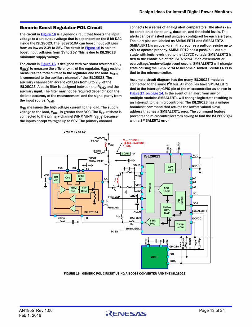
Generic LDO Regulator POL CircuitLow Dropout (LDO) voltage regulators are mostly used in applications that require a regulated supply while a minimum voltage difference exists between the applied voltage to the regulator and the regulated voltage. A battery application is an example where an LDO may be used. LDO’s may also be used in noise sensitive applications. There is no internal clock or switching signals within an LDO. Because of the lack of switching circuitry, the output regulated signal does not have noise compared to a buck regulator. Applications that are sensitive to EMI susceptibility may use an LDO.
The circuit in Figure 15 converts the bus voltage, which is between 3V and 6V to a lower regulated voltage that can be as high as 400mV from the bus voltage applied to the ISL80101ADJ. The output voltage to the load is set via the 8-bit DAC, R2 and R1. R3 is used to more precisely tune the output voltage. For most applications, R3 is not installed. The 8-bit DAC within is the ISL28023 has many voltage ranges allowing for more precision. VOUT to a load can be calculated using:
RSH in Figure 15 is a shunt resistor that converts the current delivered to the load to a voltage. The voltage is measured by the ISL28023. The full-scale voltage of the shunt inputs (VINP-VINM) is ±80mV. The value of the shunt resistor is digitized internally to the ISL28023 enabling the device to report current measurements.
The ISL28023 has analog comparators with user defined programmable digital thresholds. The comparator circuitry allows for inputs of the primary channel (VINP, VINM, VBUS) to be tested versus programmable levels. The ISL28023 has two
SMBALERT pins. In Figure 15, SMBALERT1 is an open-drain pin connected to the enable pin of the ISL80101ADJ. In the event of an alert, the SMBALERT1 pin changes state causing the ISL80101ADJ to become disabled. The SMBALERT2 has a push/pull output with logic levels tied to the I2CVCC voltage. The SMBALERT2 is tied to the interrupt pin of the microcontroller. An unacceptable event on the primary channel will alert the microcontroller.
The I2CVCC can either be tied to the VCC pin of the ISL28023 or to the power supply pin of the microcontroller. The I2CVCC pin controls the operating voltage of the ISL28023 digital core. The I2C/SMBus/PMBus inputs and SMBALERT pins logic levels are a slave to the I2CVCC voltage.
The ISL28023’s auxiliary shunt channel (Aux_N,Aux_P) can be programmed to change functionality from measuring a voltage between ±80mV to measuring a temperature through a diode. In the external temperature mode, a current source injects two currents (20µA/ 100µA) into an external diode measuring the change in diode voltage between the two currents. The change in diode voltage translates to a temperature. Diodes are good at accurately measuring temperature change. A user may want to measure the temperature change of a resistor for accurate current measurements. In high current applications, the material of a resistor consists mostly of metal. Metal has a high temperature coefficient. Monitoring the temperature change of a resistor allows for compensation of resistance change due to temperature.
The AUXV pin measures the regulated voltage to load. The AUXV pin measures voltages up to the VCC voltage of the ISL28023 chip. For the circuit in Figure 15, the maximum measurable voltage for the AuxV channel is the bus voltage to the circuit, VIN.
(EQ. 17)VOUT 0.5 0.5 DAC_OUT–
R2R1-------+=
FIGURE 15. GENERIC POL CIRCUIT USING A LDO CONVERTER AND THE ISL28023
LO
AD
VOUT = 0.5 + (0.5 – DAC OUT) * R2/R1
I2C
SM
BU
S
A1
SCL
SDA
VINPGND
ADC 16-Bit
SW
MU
X
PMBus REGMAP
A0
ISL28023VCC
VINM
VBUS
VIN
SMBALERT1
A2
8-BitDAC
DAC OUT
VIN = 3V TO 6V
R2
R1
R3
Vm
cu
GN
D
GPIO/Int
SDAGPIO
SCL
R_
pu
llU
p
R_
pu
llUp
MCU
SMBALERT2
I2CVCC
3.3VVreg
Vre
g_
in
Vre
g_
Ou
t
VIN
RSH
AUXV
AUXP
AUXM
Ext_TempPlace Diode
Near RSH
ADJ
Error AmpVref
VOUT
ISL
80
10
1-A
DJ
EN
LDO
+-
PG
Current Buffer
TempSense
AN1955 Rev 1.00 Page 12 of 24Feb 1, 2016
Design Ideas for Intersil Digital Power Monitors
Generic Boost Regulator POL CircuitThe circuit in Figure 16 is a generic circuit that boosts the input voltage to a set output voltage that is dependent on the 8-bit DAC inside the ISL28023. The ISL97519A can boost input voltages from as low as 2.3V to 25V. The circuit in Figure 16 is able to boost input voltages from 3V to 25V. This is due to ISL28023 minimum supply voltage.
The circuit in Figure 16 is designed with two shunt resistors (RSH, RSH2) to measure the efficiency, η, of the regulator. RSH2 resistor measures the total current to the regulator and the load. RSH2 is connected to the auxiliary channel of the ISL28023. The auxiliary channel can accept voltages from 0 to VCC of the ISL28023. A basic filter is designed between the RSH2 and the auxiliary input. The filter may not be required depending on the desired accuracy of the measurement, and the signal purity from the input source, Vrail.
RSH measures the high voltage current to the load. The supply voltage to the load, VOUT, is greater than VCC. The RSH resistor is connected to the primary channel (VINP, VINM, VBUS) because the inputs accept voltages up to 60V. The primary channel
connects to a series of analog alert comparators. The alerts can be conditioned for polarity, duration, and threshold levels. The alerts can be masked and uniquely configured for each alert pin. The alert pins are labeled as SMBALERT1 and SMBALERT2. SMBALERT1 is an open-drain that requires a pull-up resistor up to 20V to operate properly. SMBALERT2 has a push/pull output stage with logic levels tied to the I2CVCC voltage. SMBALERT2 is tied to the enable pin of the ISL97519A. If an overcurrent or overvoltage/undervoltage event occurs, SMBALERT2 will change state causing the ISL97519A to become disabled. SMBALERT1 is tied to the microcontroller.
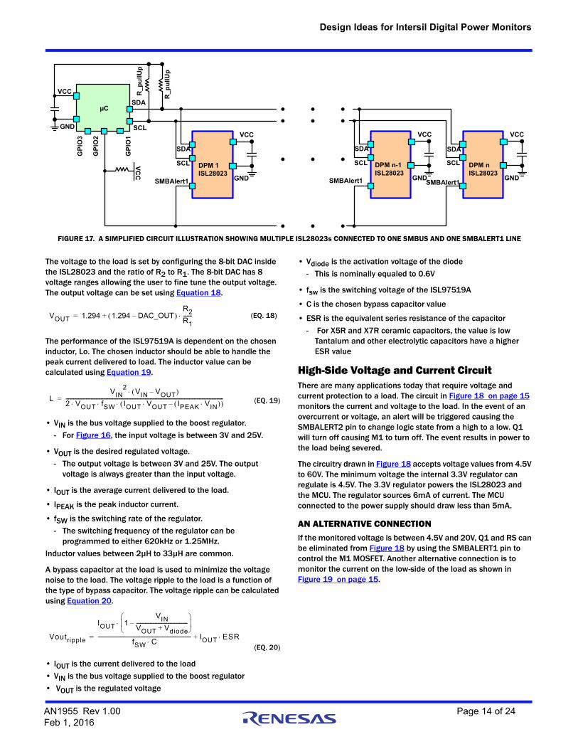
Assume a circuit diagram has the many ISL28023 modules connected to the same I2C bus. All modules have SMBALERT1 tied to the interrupt/GPIO pin of the microcontroller as shown in Figure 17 on page 14. In the event of an alert from any or multiple modules SMBALERT1 will change logic state resulting in an interrupt to the microcontroller. The ISL28023 has a unique broadcast command that returns the lowest valued slave address that has a SMBALERT1 error. The command feature prevents the microcontroller from having to find the ISL28023(s) with a SMBALERT1 error.
FIGURE 16. GENERIC POL CIRCUIT USING A BOOST CONVERTER AND THE ISL28023
R SH
Vrail = 3V to 5V
LOAD
RefGen
Osc Cntrl En
PWMCntrl
FETDrive
ISL97519A
Comp
VDD
FB
GND
LX
SSENFSEL
FROM SMBALERT2
TO EN
I2 CSM
BUS
A1
SCL
SDA
VINP
GND
ADC 16-Bit
A0
ISL28023 VCC
VINM
VBUS
SMBALERT2
A2
8-BitDAC
DAC OUTR2
R1
Vmcu
GN
D
GPIO/Int
SDA
SCL
R_pu
llUp
R_pu
llUp
MCU
SMBALERT1
I2CVCC
3.3VVreg
Vreg
_in
Vreg
_Out
AUXV
AUXP
AUXM
TempSense
R_pu
llUp
PMBus REGMAP
Lo
SW M
UX
From AxP
From AxN
VOUT = 1.294 + (1.294 – DAC OUT) * R2/R1
Rsh2
To AxP
To AxN
AN1955 Rev 1.00 Page 13 of 24Feb 1, 2016
Design Ideas for Intersil Digital Power Monitors
The voltage to the load is set by configuring the 8-bit DAC inside the ISL28023 and the ratio of R2 to R1. The 8-bit DAC has 8 voltage ranges allowing the user to fine tune the output voltage. The output voltage can be set using Equation 18.
The performance of the ISL97519A is dependent on the chosen inductor, Lo. The chosen inductor should be able to handle the peak current delivered to load. The inductor value can be calculated using Equation 19.
• VIN is the bus voltage supplied to the boost regulator.
- For Figure 16, the input voltage is between 3V and 25V.
• VOUT is the desired regulated voltage.
- The output voltage is between 3V and 25V. The output voltage is always greater than the input voltage.
• IOUT is the average current delivered to the load.
• IPEAK is the peak inductor current.
• fSW is the switching rate of the regulator.
- The switching frequency of the regulator can be programmed to either 620kHz or 1.25MHz.
Inductor values between 2µH to 33µH are common.
A bypass capacitor at the load is used to minimize the voltage noise to the load. The voltage ripple to the load is a function of the type of bypass capacitor. The voltage ripple can be calculated using Equation 20.
• IOUT is the current delivered to the load
• VIN is the bus voltage supplied to the boost regulator
• VOUT is the regulated voltage
• Vdiode is the activation voltage of the diode
- This is nominally equaled to 0.6V
• fsw is the switching voltage of the ISL97519A
• C is the chosen bypass capacitor value
• ESR is the equivalent series resistance of the capacitor
- For X5R and X7R ceramic capacitors, the value is low Tantalum and other electrolytic capacitors have a higher ESR value
High-Side Voltage and Current CircuitThere are many applications today that require voltage and current protection to a load. The circuit in Figure 18 on page 15 monitors the current and voltage to the load. In the event of an overcurrent or voltage, an alert will be triggered causing the SMBALERT2 pin to change logic state from a high to a low. Q1 will turn off causing M1 to turn off. The event results in power to the load being severed.
The circuitry drawn in Figure 18 accepts voltage values from 4.5V to 60V. The minimum voltage the internal 3.3V regulator can regulate is 4.5V. The 3.3V regulator powers the ISL28023 and the MCU. The regulator sources 6mA of current. The MCU connected to the power supply should draw less than 5mA.
AN ALTERNATIVE CONNECTIONIf the monitored voltage is between 4.5V and 20V, Q1 and RS can be eliminated from Figure 18 by using the SMBALERT1 pin to control the M1 MOSFET. Another alternative connection is to monitor the current on the low-side of the load as shown in Figure 19 on page 15.
FIGURE 17. A SIMPLIFIED CIRCUIT ILLUSTRATION SHOWING MULTIPLE ISL28023s CONNECTED TO ONE SMBUS AND ONE SMBALERT1 LINE
µC
VCC
GNDG
PIO
1
GP
IO2
SDA
SCL
GP
IO3
DPM 1ISL28023
VCC
GND
SDA
SCL DPM n-1ISL28023
VCC
GND
SDA
SCL
SMBAlert1 SMBAlert1
R_
pu
llU
p
R_
pu
llU
pDPM nISL28023
VCC
GND
SDA
SCL
SMBAlert1
VC
C
(EQ. 18)VOUT 1.294 1.294 DAC_OUT– R2R1-------+=
(EQ. 19)LVIN
2VIN VOUT–
2 VOUT fSW IOUT VOUT IPEAK VIN – -----------------------------------------------------------------------------------------------------------------------------=
(EQ. 20)Voutripple
IOUT 1VIN
VOUT Vdiode+-----------------------------------------–
fSW C-------------------------------------------------------------------------- IOUT ESR+=
AN1955 Rev 1.00 Page 14 of 24Feb 1, 2016
Design Ideas for Intersil Digital Power Monitors
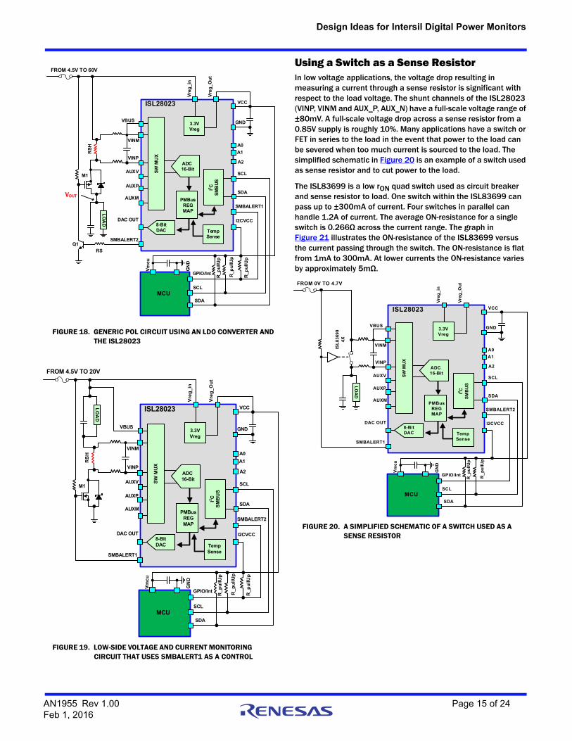
Using a Switch as a Sense ResistorIn low voltage applications, the voltage drop resulting in measuring a current through a sense resistor is significant with respect to the load voltage. The shunt channels of the ISL28023 (VINP, VINM and AUX_P, AUX_N) have a full-scale voltage range of ±80mV. A full-scale voltage drop across a sense resistor from a 0.85V supply is roughly 10%. Many applications have a switch or FET in series to the load in the event that power to the load can be severed when too much current is sourced to the load. The simplified schematic in Figure 20 is an example of a switch used as sense resistor and to cut power to the load.
The ISL83699 is a low rON quad switch used as circuit breaker and sense resistor to load. One switch within the ISL83699 can pass up to ±300mA of current. Four switches in parallel can handle 1.2A of current. The average ON-resistance for a single switch is 0.266Ω across the current range. The graph in Figure 21 illustrates the ON-resistance of the ISL83699 versus the current passing through the switch. The ON-resistance is flat from 1mA to 300mA. At lower currents the ON-resistance varies by approximately 5mΩ.
FIGURE 18. GENERIC POL CIRCUIT USING AN LDO CONVERTER AND THE ISL28023
FIGURE 19. LOW-SIDE VOLTAGE AND CURRENT MONITORING CIRCUIT THAT USES SMBALERT1 AS A CONTROL
RSH
LOA
D
I2 CSM
BUS
A1
SCL
SDA
VINP
GND
ADC 16-Bit
A0
ISL28023 VCC
VINM
VBUS
SMBALERT2
A2
8-BitDAC
DAC OUT
Vmcu
GN
D
GPIO/Int
SDA
SCL
R_pu
llUp
R_pu
llUp
MCU
SMBALERT1
I2CVCC
3.3VVreg
Vreg
_in
Vreg
_Out
AUXV
AUXP
AUXM
TempSense
PMBus REGMAP
SW M
UX
VOUT
FROM 4.5V TO 60V
Q1
M1
R_pu
llUp
RS
RS
H
LO
AD
I2C
SM
BU
S
A1
SCL
SDA
VINP
GND
ADC 16-Bit
A0
ISL28023 VCC
VINM
VBUS
SMBALERT1
A2
8-BitDAC
DAC OUT
Vm
cu
GN
D
GPIO/Int
SDA
SCL
R_
pu
llUp
R_
pu
llU
p
MCU
SMBALERT2
I2CVCC
3.3VVreg
Vre
g_
in
Vre
g_
Ou
t
AUXV
AUXP
AUXM
TempSense
PMBus REGMAP
SW
MU
X
FROM 4.5V TO 20V
M1
R_
pu
llU
p
FIGURE 20. A SIMPLIFIED SCHEMATIC OF A SWITCH USED AS A SENSE RESISTOR
LO
AD I2
CS
MB
US
A1
SCL
SDA
VINP
GND
ADC 16-Bit
A0
ISL28023 VCC
VINM
VBUS
SMBALERT1
A2
8-BitDAC
DAC OUT
Vm
cu
GN
D
GPIO/Int
SDA
SCL
R_
pu
llU
p
R_
pu
llU
p
MCU
SMBALERT2
I2CVCC
3.3VVreg
Vre
g_
in
Vre
g_
Ou
t
AUXV
AUXP
AUXM
TempSense
PMBus REGMAP
SW
MU
X
FROM 0V TO 4.7V
ISL
83
69
94
X
AN1955 Rev 1.00 Page 15 of 24Feb 1, 2016
Design Ideas for Intersil Digital Power Monitors
Connecting four switches in parallel divides the rON resistance by four as well as the variance across current. The sense resistor becomes 66.5mΩ.
The full-scale range of the primary shunt input is ±80mV. From Ohms law, the maximum current that is measured for 67mΩ sensing element is 1.2A. The application may require the highest resolution for measurable currents to 750mA. The VSHUNT reading for 750mA of current with a 67mΩ sensing element is 49.88mV. The ISL28023 has configurable current range. The LSB (Least Significant Bit) is calculated by using Equation 21.
CurrentFS is the full-scale measurable current or 750mA for this application. ADCres is 15 bits in one current direction (0mA to 750mA). The ISL28023 calculates the current for each reading if the CalReg is programmed properly. The CalReg is calculated using Equation 22.
The current measurement for the primary shunt can be read from register 0x8C. The decimal current is calculated using Equation 23.
Reg_0x8Cvalue is the value returned from reading register 0x8C of the ISL28023. CurrentLSB is the value from Equation 21.
4 Gas Sensing CircuitGas monitoring is prevalent in safety and manufacturing applications. Gas sensing, more specifically electrochemical gas sensing, keeps miners safe from such toxins as hydrogen sulfide (H2S) and carbon monoxide (CO). Households in the US are required to have CO detectors along with fire detectors for air quality protection. The food industry is using gas sensors to
determine the freshness of food at fisheries and at the supermarket. In the manufacturing process, gas sensors are used to monitor the amount of gas element transferred from one medium to another.
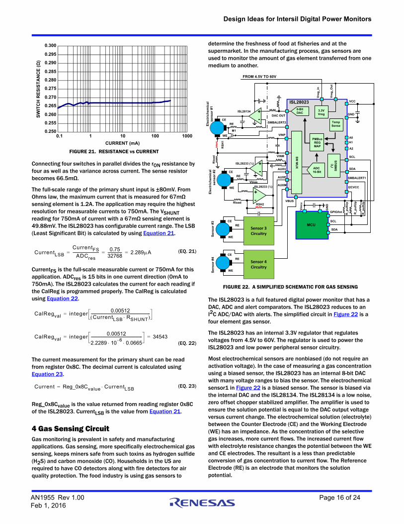
The ISL28023 is a full featured digital power monitor that has a DAC, ADC and alert comparators. The ISL28023 reduces to an I2C ADC/DAC with alerts. The simplified circuit in Figure 22 is a four element gas sensor.
The ISL28023 has an internal 3.3V regulator that regulates voltages from 4.5V to 60V. The regulator is used to power the ISL28023 and low power peripheral sensor circuitry.
Most electrochemical sensors are nonbiased (do not require an activation voltage). In the case of measuring a gas concentration using a biased sensor, the ISL28023 has an internal 8-bit DAC with many voltage ranges to bias the sensor. The electrochemical sensor1 in Figure 22 is a biased sensor. The sensor is biased via the internal DAC and the ISL28134. The ISL28134 is a low noise, zero offset chopper stabilized amplifier. The amplifier is used to ensure the solution potential is equal to the DAC output voltage versus current change. The electrochemical solution (electrolyte) between the Counter Electrode (CE) and the Working Electrode (WE) has an impedance. As the concentration of the selective gas increases, more current flows. The increased current flow with electrolyte resistance changes the potential between the WE and CE electrodes. The resultant is a less than predictable conversion of gas concentration to current flow. The Reference Electrode (RE) is an electrode that monitors the solution potential.
FIGURE 21. RESISTANCE vs CURRENT
0.250
0.255
0.260
0.265
0.270
0.275
0.280
0.285
0.290
0.295
0.300
0.1 1 10 100 1000
CURRENT (mA)
SW
ITC
H R
ES
IST
AN
CE
(Ω
)
(EQ. 21)CurrentLSB
CurrentFSADCres
------------------------------ 0.7532768---------------- 2.289A= = =
(EQ. 22)
CalRegval integer0.00512
CurrentLSB RSHUNT -------------------------------------------------------------------=
CalRegval integer0.00512
2.2289 106–
0.0665 ---------------------------------------------------------- 34543= =
(EQ. 23)Current Reg_0x8Cvalue CurrentLSB=
FIGURE 22. A SIMPLIFIED SCHEMATIC FOR GAS SENSING
I2C
SM
BU
S
A1
SCL
SDA
VINP
GND
ADC 16-Bit
A0
ISL28023 VCC
VINM
VBUS
SMBALERT2
A2
8-BitDAC
DAC OUT
Vm
cu
GN
D
GPIO/Int
SDA
SCL
R_
pu
llUp
R_
pu
llU
p
MCU
SMBALERT1
I2CVCC
Vre
g_
in
Vre
g_
Ou
t
AUXV
AUXP
AUXM
TempSense
PMBus REGMAP
SW
MU
X
FROM 4.5V TO 60V
3.3VVreg
Ele
ctri
ch
em
ica
l s
en
so
r #
1
WE
CE
RE
ISL28134
Rlo
ad
RS
H1
+
-
WE
CE
RE
Ele
ctr
ich
em
ical
s
en
sor
#2
WE
CE
RE
ISL28233 (½) +
-
+
-
RloadRSH2
ISL28233 (½)
R_
pu
llU
p
M1
Se
ns
or
#3
WE
CE
RE
Se
ns
or
#4
Sensor 3Circuitry
Sensor 4Circuitry
Vbias
AN1955 Rev 1.00 Page 16 of 24Feb 1, 2016
Design Ideas for Intersil Digital Power Monitors
Most electrochemical sensors require a load resistance to linearize the resistors performance. The primary shunt channel (VINM. VINP) is connected to a shunt resistor (RSH) to measure current flow of the sensor. The magnitude of current translates to a gas concentration. The shunt resistor may also be used as the load resistance to the sensor. The ISL28023 internally calculates the current once the shunt resistor value is programmed into the IC.
The working electrode of an electrochemical sensor has a chemical agent attracting the gas of interest to the electrode. Usually, a filter is employed between the working electrode and the outside world to prevent compounds and like elements from interacting with the electrode. The filter prevents false concentration readings.
Care should be observed in powering an electrochemical sensor as well as when the sensor sits at rest. If reversed potentials are applied to the sensor, this causes the attracting agent to be stripped from the working electrode and deposited into the electrolyte and ultimately onto the counter electrode. The event as described reduces the lifetime of the sensor and changes the response of the sensor. M1, which is driven by the SMBALERT2 pin of the ISL28023, shorts the reference electrode to the working electrode. The shorting of WE and RE eliminates a path for the reacting agent to deposit to. The SMBALERT2 can be configured to an activation polarity and can be forced to a state.
Electrochemical sensor 2 is a nonbiased sensor that employs the use of the ISL28233 dual chopper amplifier. One amplifier of the dual amplifier is used to maintain the electrolyte potential. The second amplifier is a transimpedance amplifier that converts current to voltage. The voltage output equation for the transimpedance amplifier is represented in Equation 24.
Isensor is the current flowing to or from the sensor. The magnitude of current represents the concentration of gas in the medium. RSH2 is the gain resistor that converts the current to a voltage. Vbias is the operating voltage of the transimpedance amplifier.
Connected to the primary channel of the ISL28023 are analog comparators that can send alerts via the SMBALERT1 pin to the microcontroller. The compare potentials of the analog comparators represent the concentration values of each sensor.
Sensor blocks 3 and 4 could be circuitry for electrochemical sensors or any other sensors that feed into the auxiliary channel of the ISL28023. See “Combustible Gas Sensor Circuit” on page 7.
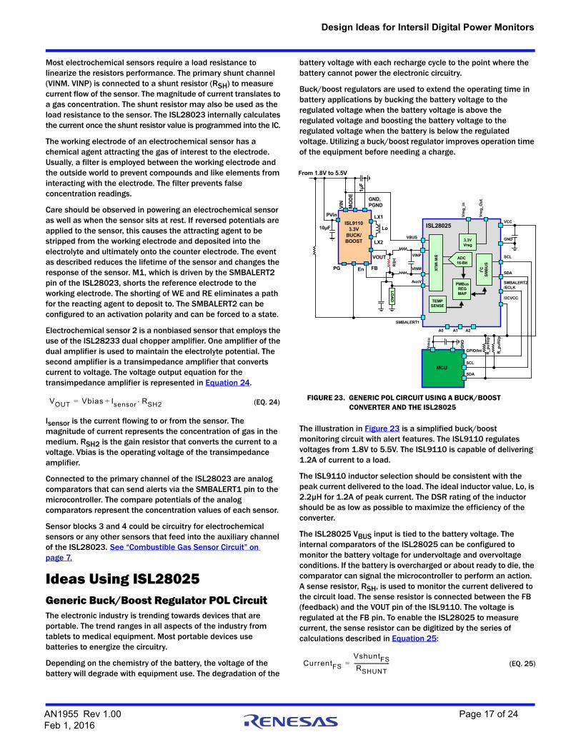
Ideas Using ISL28025Generic Buck/Boost Regulator POL CircuitThe electronic industry is trending towards devices that are portable. The trend ranges in all aspects of the industry from tablets to medical equipment. Most portable devices use batteries to energize the circuitry.
Depending on the chemistry of the battery, the voltage of the battery will degrade with equipment use. The degradation of the
battery voltage with each recharge cycle to the point where the battery cannot power the electronic circuitry.
Buck/boost regulators are used to extend the operating time in battery applications by bucking the battery voltage to the regulated voltage when the battery voltage is above the regulated voltage and boosting the battery voltage to the regulated voltage when the battery is below the regulated voltage. Utilizing a buck/boost regulator improves operation time of the equipment before needing a charge.
The illustration in Figure 23 is a simplified buck/boost monitoring circuit with alert features. The ISL9110 regulates voltages from 1.8V to 5.5V. The ISL9110 is capable of delivering 1.2A of current to a load.
The ISL9110 inductor selection should be consistent with the peak current delivered to the load. The ideal inductor value, Lo, is 2.2µH for 1.2A of peak current. The DSR rating of the inductor should be as low as possible to maximize the efficiency of the converter.
The ISL28025 VBUS input is tied to the battery voltage. The internal comparators of the ISL28025 can be configured to monitor the battery voltage for undervoltage and overvoltage conditions. If the battery is overcharged or about ready to die, the comparator can signal the microcontroller to perform an action. A sense resistor, RSH, is used to monitor the current delivered to the circuit load. The sense resistor is connected between the FB (feedback) and the VOUT pin of the ISL9110. The voltage is regulated at the FB pin. To enable the ISL28025 to measure current, the sense resistor can be digitized by the series of calculations described in Equation 25:
(EQ. 24)VOUT Vbias Isensor+ RSH2= FIGURE 23. GENERIC POL CIRCUIT USING A BUCK/BOOST CONVERTER AND THE ISL28025
LO
AD
I2 CS
MB
US
A1
SCL
SDA
VINP
GND
ADC 16-Bit
A0
ISL28025VCC
VINM
VBUS
SMBALERT1
A2
Vm
cu
GN
D
GPIO/Int
SDA
SCL
R_
pu
llUp
R_p
ullU
p
MCU
SMBALERT2 /ECLK
I2CVCC
3.3VVreg
Vre
g_
in
Vre
g_O
ut
AuxV
TEMPSENSE
PMBus REGMAP
SW
MU
X
From 1.8V to 5.5V
VOUT
FB
ISL91103.3V
BUCK/BOOST
EnPG
GND,PGNDM
OD
E
PVin
Lo
VIN
1µF
LX2
LX1
10µF
RS
H
(EQ. 25)CurrentFS
VshuntFSRSHUNT----------------------------=
AN1955 Rev 1.00 Page 17 of 24Feb 1, 2016
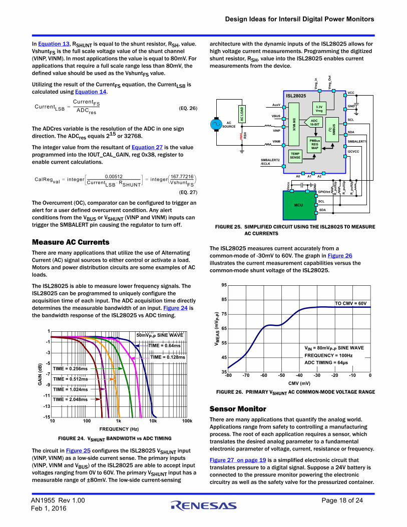
Design Ideas for Intersil Digital Power Monitors
In Equation 13, RSHUNT is equal to the shunt resistor, RSH, value. VshuntFS is the full scale voltage value of the shunt channel (VINP, VINM). In most applications the value is equal to 80mV. For applications that require a full scale range less than 80mV, the defined value should be used as the VshuntFS value.
Utilizing the result of the CurrentFS equation, the CurrentLSB is calculated using Equation 14.
The ADCres variable is the resolution of the ADC in one sign direction. The ADCres equals 215 or 32768.
The integer value from the resultant of Equation 27 is the value programmed into the IOUT_CAL_GAIN, reg 0x38, register to enable current calculations.
The Overcurrent (OC), comparator can be configured to trigger an alert for a user defined overcurrent condition. Any alert conditions from the VBUS or VSHUNT (VINP and VINM) inputs can trigger the SMBALERT pin causing the regulator to turn off.
Measure AC CurrentsThere are many applications that utilize the use of Alternating Current (AC) signal sources to either control or activate a load. Motors and power distribution circuits are some examples of AC loads.
The ISL28025 is able to measure lower frequency signals. The ISL28025 can be programmed to uniquely configure the acquisition time of each input. The ADC acquisition time directly determines the measurable bandwidth of an input. Figure 24 is the bandwidth response of the ISL28025 vs ADC timing.
The circuit in Figure 25 configures the ISL28025 VSHUNT input (VINP, VINM) as a low-side current sense. The primary inputs (VINP, VINM and VBUS) of the ISL28025 are able to accept input voltages ranging from 0V to 60V. The primary VSHUNT input has a measurable range of ±80mV. The low-side current-sensing
architecture with the dynamic inputs of the ISL28025 allows for high voltage current measurements. Programming the digitized shunt resistor, RSH, value into the ISL28025 enables current measurements from the device.
The ISL28025 measures current accurately from a common-mode of -30mV to 60V. The graph in Figure 26 illustrates the current measurement capabilities versus the common-mode shunt voltage of the ISL28025.
Sensor MonitorThere are many applications that quantify the analog world. Applications range from safety to controlling a manufacturing process. The root of each application requires a sensor, which translates the desired analog parameter to a fundamental electronic parameter of voltage, current, resistance or frequency.
Figure 27 on page 19 is a simplified electronic circuit that translates pressure to a digital signal. Suppose a 24V battery is connected to the pressure monitor powering the electronic circuitry as well as the safety valve for the pressurized container.
FIGURE 24. VSHUNT BANDWIDTH vs ADC TIMING
(EQ. 26)CurrentLSB
CurrentFSADCres
------------------------------=
(EQ. 27)
CalRegval integer0.00512
CurrentLSB RSHUNT------------------------------------------------------------------ integer
167.77216VshuntFS----------------------------- = =
-15
-13
-11
-9
-7
-5
-3
-1
1
10 100 1k 10k 100k
FREQUENCY (Hz)
GA
IN (
dB
)
TIME = 0.128ms
50mVP-P SINE WAVE
TIME = 0.64ms
TIME = 0.256ms
TIME = 1.024ms
TIME = 2.048ms
TIME = 0.512ms
FIGURE 25. SIMPLIFIED CIRCUIT USING THE ISL28025 TO MEASURE AC CURRENTS
FIGURE 26. PRIMARY VSHUNT AC COMMON-MODE VOLTAGE RANGE
I2C
SM
BU
S
A1
SCL
SDAVINP
GND
ADC 16-BIT
A0
ISL28025VCC
VINM
VBUS
SMBALERT2/ECLK
A2
Vm
cu
GN
D
GPIO/Int
SDA
SCL
R_
pu
llUp
R_p
ullU
p
MCU
SMBALERT1
I2CVCC
3.3VVreg
Vre
g_
in
Vre
g_
Ou
t
AuxV
TEMPSENSE
PMBus REGMAP
SW
MU
X
R_
pu
llUp
RS
HA
C L
OA
D
AC SOURCE
35
45
55
65
75
85
95
-80 -70 -60 -50 -40 -30 -20 -10 0
CMV (mV)
VM
EA
S (
mV
P-P
)
TO CMV = 60V
VIN = 80mVP-P SINE WAVE
FREQUENCY = 100Hz
ADC TIMING = 64µs
AN1955 Rev 1.00 Page 18 of 24Feb 1, 2016
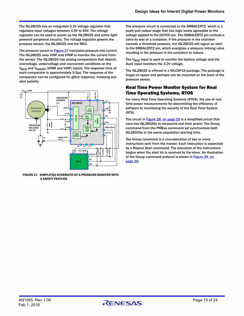
Design Ideas for Intersil Digital Power Monitors
The ISL28025 has an integrated 3.3V voltage regulator that regulates input voltages between 4.5V to 60V. The voltage regulator can be used to power up the ISL28025 and some light powered peripheral circuitry. The voltage regulator powers the pressure sensor, the ISL28025 and the MCU.
The pressure sensor in Figure 27 translates pressure into current. The ISL28025 uses VINP and VINM to monitor the current from the sensor. The ISL28025 has analog comparators that detects overvoltage, undervoltage and overcurrent conditions on the VBUS and VSHUNT (VINM and VINP) inputs. The response time of each comparator is approximately 0.5µs. The response of the comparator can be configured for glitch response, masking and alert polarity.
The pressure circuit is connected to the SMBALERT2, which is a push/pull output stage that has logic levels agreeable to the voltage applied to the I2CVCC pin. The SMBALERT2 pin controls a valve by way of a transistor. If the pressure in the chamber exceeds a threshold pressure, the ISL28025 will signal an alert to the SMBALERT2 pin, which energizes a pressure reliving valve resulting in the pressure in the container to reduce.
The VBUS input is used to monitor the battery voltage and the AuxV input monitors the 3.3V voltage.
The ISL28025 is offered in a WLCSP16 package. The package is frugal on space and perhaps can be mounted on the back of the pressure sensor.
Real Time Power Monitor System for Real Time Operating Systems, RTOSFor many Real Time Operating Systems (RTOS), the use of real time power measurements for determining the efficiency of software to monitoring the security of the Real Time System (RTS).
The circuit in Figure 28 on page 20 is a simplified circuit that uses two ISL28025s to measured real time power. The Group command from the PMBus command set synchronizes both ISL28025s to the same acquisition starting time.
The Group command is a concatenation of two or more instructions sent from the master. Each instruction is separated by a Repeat Start command. The execution of the instructions begins when the start bit is received by the slave. An illustration of the Group command protocol is shown in Figure 29 on page 20.
FIGURE 27. SIMPLIFIED SCHEMATIC OF A PRESSURE MONITOR WITH A SAFETY FEATURE
I2 CS
MB
US
A1
SCL
SDAVINP
GND
ADC 16-Bit
A0
ISL28025VCC
VINM
VBUS
SMBALERT2/ECLK
A2
Vm
cu
GN
D
GPIO/Int
SDA
SCL
R_p
ullU
p
R_
pu
llUp
MCU
SMBALERT1
I2CVCC
3.3VVREG
Vre
g_i
n
Vre
g_O
ut
AuxV
TEMPSENSE
PMBus REGMAP
SW
MU
X
VBAT = 24V
PRESSURE RELEASE VALVE
PRESSURE SENSORIOUT
RS
H/
RL
OA
D
Pressurized Container
M1
R_p
ullU
p
AN1955 Rev 1.00 Page 19 of 24Feb 1, 2016
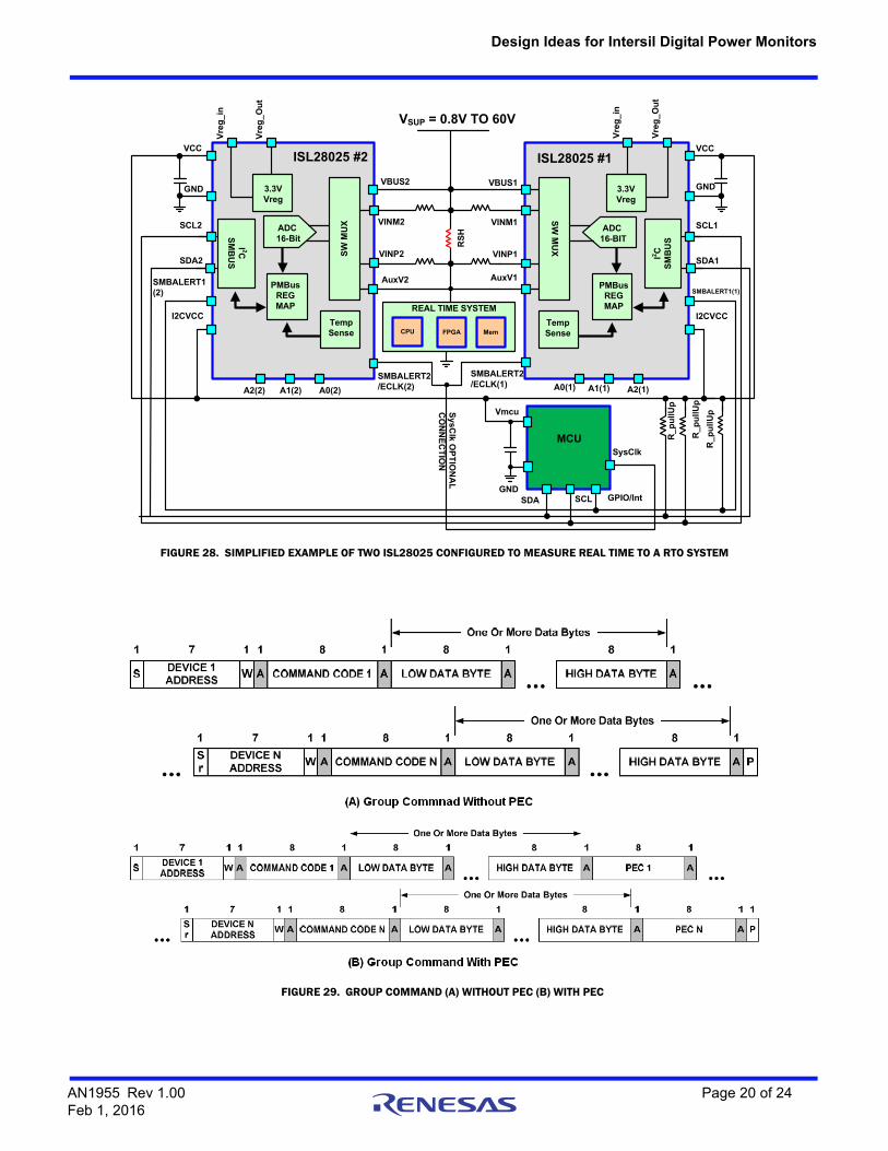
Design Ideas for Intersil Digital Power Monitors
FIGURE 28. SIMPLIFIED EXAMPLE OF TWO ISL28025 CONFIGURED TO MEASURE REAL TIME TO A RTO SYSTEM
I2 CS
MB
US
A1(1)
SCL1
SDA1VINP1
GND
ADC 16-BIT
A0(1)
ISL28025 #1VCC
VINM1
VBUS1
SMBALERT2/ECLK(1)
A2(1)
R_p
ullU
p
R_p
ull
Up
SMBALERT1(1)
I2CVCC
3.3VVreg
Vre
g_i
n
Vre
g_O
ut
AuxV1
TempSense
PMBus REGMAP
SW
MU
XRS
H
I 2CS
MB
US
A1(2)
SCL2
SDA2VINP2
GND
ADC 16-Bit
A0(2)
ISL28025 #2VCC
VINM2
A2(2)
SMBALERT1 (2)
I2CVCC
3.3VVreg
AuxV2
TempSense
PMBus REGMAP
SW
MU
X
VBUS2
SMBALERT2/ECLK(2)
GNDGPIO/IntSDA SCL
MCU
Vmcu
REAL TIME SYSTEM
CPU FPGA Mem
VSUP = 0.8V TO 60V
R_p
ull
Up
Vre
g_i
n
Vre
g_O
ut
SysClk
SysC
lk OP
TIO
NA
L
CO
NN
EC
TIO
N
FIGURE 29. GROUP COMMAND (A) WITHOUT PEC (B) WITH PEC
AN1955 Rev 1.00 Page 20 of 24Feb 1, 2016
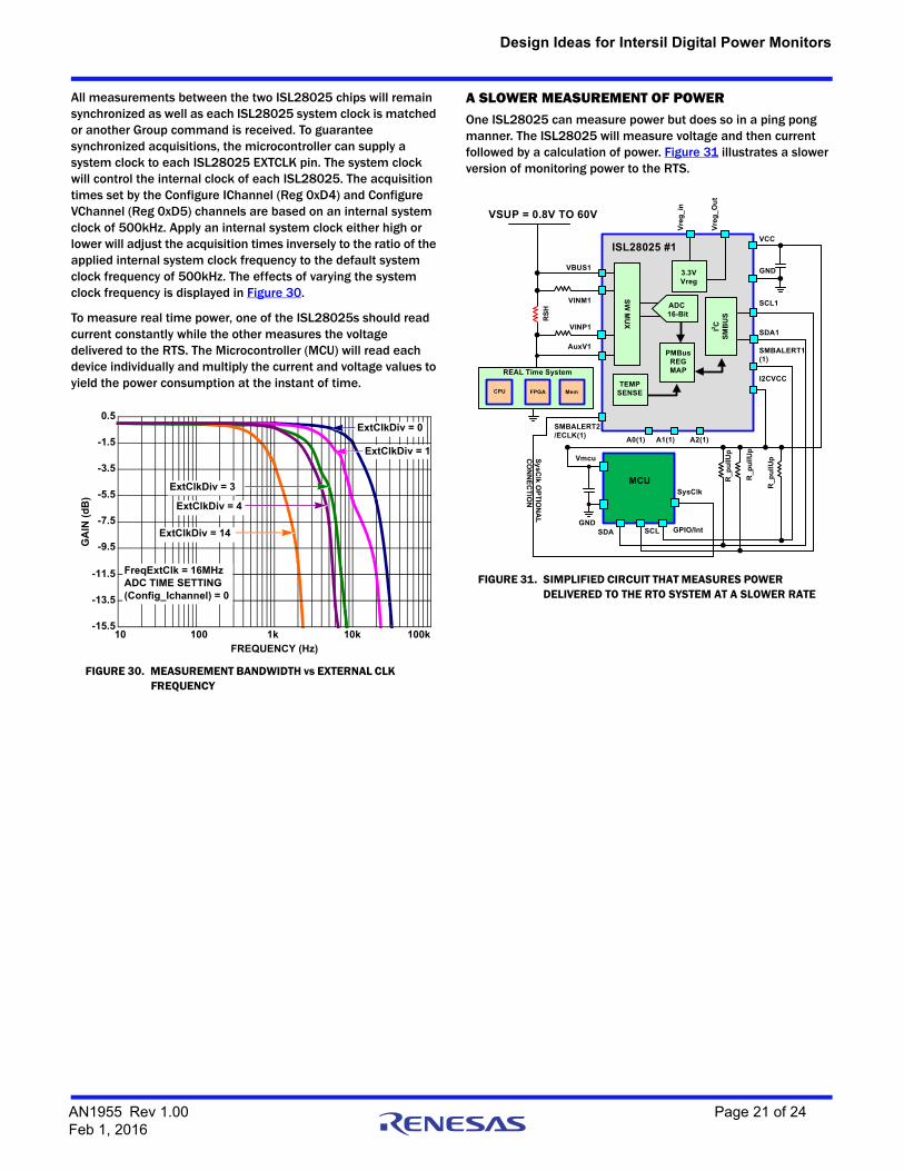
Design Ideas for Intersil Digital Power Monitors
All measurements between the two ISL28025 chips will remain synchronized as well as each ISL28025 system clock is matched or another Group command is received. To guarantee synchronized acquisitions, the microcontroller can supply a system clock to each ISL28025 EXTCLK pin. The system clock will control the internal clock of each ISL28025. The acquisition times set by the Configure IChannel (Reg 0xD4) and Configure VChannel (Reg 0xD5) channels are based on an internal system clock of 500kHz. Apply an internal system clock either high or lower will adjust the acquisition times inversely to the ratio of the applied internal system clock frequency to the default system clock frequency of 500kHz. The effects of varying the system clock frequency is displayed in Figure 30.
To measure real time power, one of the ISL28025s should read current constantly while the other measures the voltage delivered to the RTS. The Microcontroller (MCU) will read each device individually and multiply the current and voltage values to yield the power consumption at the instant of time.
A SLOWER MEASUREMENT OF POWEROne ISL28025 can measure power but does so in a ping pong manner. The ISL28025 will measure voltage and then current followed by a calculation of power. Figure 31 illustrates a slower version of monitoring power to the RTS.
FIGURE 30. MEASUREMENT BANDWIDTH vs EXTERNAL CLK FREQUENCY
-15.5
-13.5
-11.5
-9.5
-7.5
-5.5
-3.5
-1.5
0.5
10 100 1k 10k 100kFREQUENCY (Hz)
GA
IN (
dB
)
ExtClkDiv = 1
ExtClkDiv = 0
ExtClkDiv = 14
ExtClkDiv = 4
ExtClkDiv = 3
FreqExtClk = 16MHzADC TIME SETTING (Config_Ichannel) = 0
FIGURE 31. SIMPLIFIED CIRCUIT THAT MEASURES POWER DELIVERED TO THE RTO SYSTEM AT A SLOWER RATE
I2C
SM
BU
S
A1(1)
SCL1
SDA1VINP1
GND
ADC 16-Bit
A0(1)
ISL28025 #1VCC
VINM1
VBUS1
SMBALERT2/ECLK(1)
A2(1)
R_p
ullU
p
R_p
ull
Up
SMBALERT1(1)
I2CVCC
3.3VVreg
Vre
g_i
n
Vre
g_O
ut
AuxV1
TEMPSENSE
PMBus REGMAP
SW
MU
XRS
H
GNDGPIO/IntSDA SCL
MCU
Vmcu
REAL Time System
CPU FPGA Mem
VSUP = 0.8V TO 60V
R_p
ull
Up
SysClk
SysC
lk OP
TIO
NA
L
CO
NN
EC
TIO
N
AN1955 Rev 1.00 Page 21 of 24Feb 1, 2016
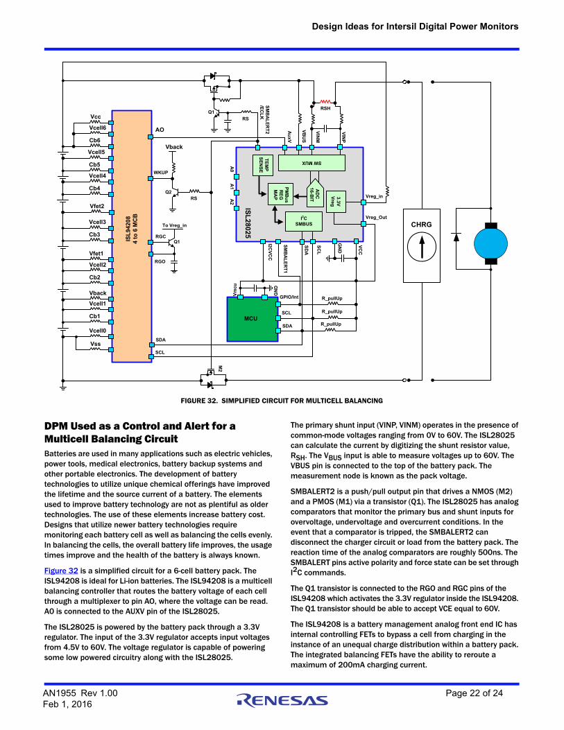
Design Ideas for Intersil Digital Power Monitors
DPM Used as a Control and Alert for a Multicell Balancing CircuitBatteries are used in many applications such as electric vehicles, power tools, medical electronics, battery backup systems and other portable electronics. The development of battery technologies to utilize unique chemical offerings have improved the lifetime and the source current of a battery. The elements used to improve battery technology are not as plentiful as older technologies. The use of these elements increase battery cost. Designs that utilize newer battery technologies require monitoring each battery cell as well as balancing the cells evenly. In balancing the cells, the overall battery life improves, the usage times improve and the health of the battery is always known.
Figure 32 is a simplified circuit for a 6-cell battery pack. The ISL94208 is ideal for Li-ion batteries. The ISL94208 is a multicell balancing controller that routes the battery voltage of each cell through a multiplexer to pin AO, where the voltage can be read. A0 is connected to the AUXV pin of the ISL28025.
The ISL28025 is powered by the battery pack through a 3.3V regulator. The input of the 3.3V regulator accepts input voltages from 4.5V to 60V. The voltage regulator is capable of powering some low powered circuitry along with the ISL28025.
The primary shunt input (VINP, VINM) operates in the presence of common-mode voltages ranging from 0V to 60V. The ISL28025 can calculate the current by digitizing the shunt resistor value, RSH. The VBUS input is able to measure voltages up to 60V. The VBUS pin is connected to the top of the battery pack. The measurement node is known as the pack voltage.
SMBALERT2 is a push/pull output pin that drives a NMOS (M2) and a PMOS (M1) via a transistor (Q1). The ISL28025 has analog comparators that monitor the primary bus and shunt inputs for overvoltage, undervoltage and overcurrent conditions. In the event that a comparator is tripped, the SMBALERT2 can disconnect the charger circuit or load from the battery pack. The reaction time of the analog comparators are roughly 500ns. The SMBALERT pins active polarity and force state can be set through I2C commands.
The Q1 transistor is connected to the RGO and RGC pins of the ISL94208 which activates the 3.3V regulator inside the ISL94208. The Q1 transistor should be able to accept VCE equal to 60V.
The ISL94208 is a battery management analog front end IC has internal controlling FETs to bypass a cell from charging in the instance of an unequal charge distribution within a battery pack. The integrated balancing FETs have the ability to reroute a maximum of 200mA charging current.
FIGURE 32. SIMPLIFIED CIRCUIT FOR MULTICELL BALANCING
I2CSMBUS
A1
SC
L
SD
A
VIN
PG
ND
AD
C 16-B
IT
A0
ISL
28
025
VC
C
VIN
M
VB
US
SM
BA
LE
RT
2/E
CL
K
A2
Vm
cu
GN
D
GPIO/Int
SDA
SCL
R_pullUp
R_pullUp
MCU
SM
BA
LE
RT
1
I2CV
CC
3.3VV
reg
Vreg_in
Vreg_Out
Au
xV
TE
MP
SE
NS
E
PM
Bu
s R
EG
MA
P
SW MUXVout
ISL
9420
84
to 6
MC
B
Vcc
Vcell6
Cb6
Vcell5
Cb5
Vcell4
Cb4
Vcell3
Cb3
Vcell2
Cb2
Vcell1
Cb1
Vcell0
Vss
Vfet2
Vfet1
Vback
AO
RSH
M2
vQ1
RS
Q2RS
Vback
WKUP
R_pullUp
RGC
RGO
Q1
SDA
SCL
CHRGTo Vreg_in
AN1955 Rev 1.00 Page 22 of 24Feb 1, 2016
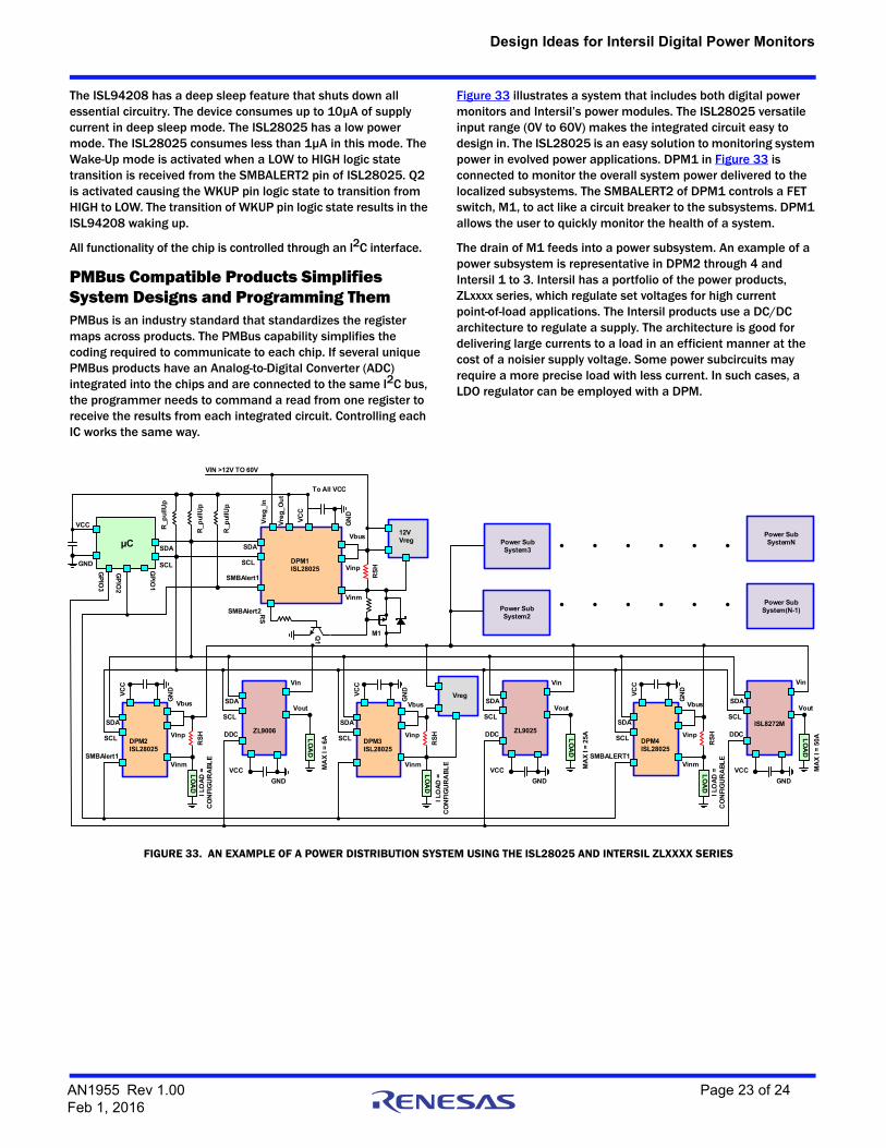
Design Ideas for Intersil Digital Power Monitors
The ISL94208 has a deep sleep feature that shuts down all essential circuitry. The device consumes up to 10µA of supply current in deep sleep mode. The ISL28025 has a low power mode. The ISL28025 consumes less than 1µA in this mode. The Wake-Up mode is activated when a LOW to HIGH logic state transition is received from the SMBALERT2 pin of ISL28025. Q2 is activated causing the WKUP pin logic state to transition from HIGH to LOW. The transition of WKUP pin logic state results in the ISL94208 waking up.
All functionality of the chip is controlled through an I2C interface.
PMBus Compatible Products Simplifies System Designs and Programming ThemPMBus is an industry standard that standardizes the register maps across products. The PMBus capability simplifies the coding required to communicate to each chip. If several unique PMBus products have an Analog-to-Digital Converter (ADC) integrated into the chips and are connected to the same I2C bus, the programmer needs to command a read from one register to receive the results from each integrated circuit. Controlling each IC works the same way.
Figure 33 illustrates a system that includes both digital power monitors and Intersil’s power modules. The ISL28025 versatile input range (0V to 60V) makes the integrated circuit easy to design in. The ISL28025 is an easy solution to monitoring system power in evolved power applications. DPM1 in Figure 33 is connected to monitor the overall system power delivered to the localized subsystems. The SMBALERT2 of DPM1 controls a FET switch, M1, to act like a circuit breaker to the subsystems. DPM1 allows the user to quickly monitor the health of a system.
The drain of M1 feeds into a power subsystem. An example of a power subsystem is representative in DPM2 through 4 and Intersil 1 to 3. Intersil has a portfolio of the power products, ZLxxxx series, which regulate set voltages for high current point-of-load applications. The Intersil products use a DC/DC architecture to regulate a supply. The architecture is good for delivering large currents to a load in an efficient manner at the cost of a noisier supply voltage. Some power subcircuits may require a more precise load with less current. In such cases, a LDO regulator can be employed with a DPM.
FIGURE 33. AN EXAMPLE OF A POWER DISTRIBUTION SYSTEM USING THE ISL28025 AND INTERSIL ZLXXXX SERIES
µC
VCC
GND
GPIO
1
GPIO
2
SDA
SCLGPIO
3
DPM2ISL28025
VCC
GN
D
ZL9006
VCCGND
SDA
SCL
SDA
SCL
DDC
SMBAlert1
R_pu
llUp
R_pu
llUp
Vbus
Vinp
Vinm
RSH
LOA
D
Vout
LOA
D
MA
X I =
6A
I LO
AD =
C
ON
FIG
UR
ABL
E
DPM4ISL28025
VCC
GN
D
ZL9025
VCCGND
SDA
SCL
SDA
SCL
DDC
Vbus
Vinp
Vinm
RSH
LOA
D
Vout
LOA
D
MA
X I =
25A
SMBALERT1
I LO
AD =
C
ON
FIG
UR
ABL
E
DPM3ISL28025
VCC
GN
D
ISL8272M
VCCGND
SDA
SCL
SDA
SCL
DDC
Vbus
Vinp
Vinm
RSH
LOA
D
Vout
LOA
D
MA
X I =
50A
I LO
AD =
C
ON
FIG
UR
ABL
E
Vreg
VinVinVin
DPM1ISL28025
VCC
GN
D
SDA
SCL
SMBAlert1
Vbus
Vinp
Vinm
RSH
Vreg
_Out
Vreg
_In
To All VCC
VIN >12V TO 60V
Power Sub System2
Power Sub System3
Power Sub SystemN
Power Sub System(N-1)
R_pu
llUp
12V Vreg
Q1
RS
SMBAlert2
M1
AN1955 Rev 1.00 Page 23 of 24Feb 1, 2016
http://www.renesas.comRefer to "http://www.renesas.com/" for the latest and detailed information.
Renesas Electronics America Inc.1001 Murphy Ranch Road, Milpitas, CA 95035, U.S.A.Tel: +1-408-432-8888, Fax: +1-408-434-5351Renesas Electronics Canada Limited9251 Yonge Street, Suite 8309 Richmond Hill, Ontario Canada L4C 9T3Tel: +1-905-237-2004Renesas Electronics Europe LimitedDukes Meadow, Millboard Road, Bourne End, Buckinghamshire, SL8 5FH, U.KTel: +44-1628-651-700, Fax: +44-1628-651-804Renesas Electronics Europe GmbHArcadiastrasse 10, 40472 Düsseldorf, Germany Tel: +49-211-6503-0, Fax: +49-211-6503-1327Renesas Electronics (China) Co., Ltd.Room 1709 Quantum Plaza, No.27 ZhichunLu, Haidian District, Beijing, 100191 P. R. ChinaTel: +86-10-8235-1155, Fax: +86-10-8235-7679Renesas Electronics (Shanghai) Co., Ltd.Unit 301, Tower A, Central Towers, 555 Langao Road, Putuo District, Shanghai, 200333 P. R. China Tel: +86-21-2226-0888, Fax: +86-21-2226-0999Renesas Electronics Hong Kong LimitedUnit 1601-1611, 16/F., Tower 2, Grand Century Place, 193 Prince Edward Road West, Mongkok, Kowloon, Hong KongTel: +852-2265-6688, Fax: +852 2886-9022Renesas Electronics Taiwan Co., Ltd.13F, No. 363, Fu Shing North Road, Taipei 10543, TaiwanTel: +886-2-8175-9600, Fax: +886 2-8175-9670Renesas Electronics Singapore Pte. Ltd.80 Bendemeer Road, Unit #06-02 Hyflux Innovation Centre, Singapore 339949Tel: +65-6213-0200, Fax: +65-6213-0300Renesas Electronics Malaysia Sdn.Bhd.Unit 1207, Block B, Menara Amcorp, Amcorp Trade Centre, No. 18, Jln Persiaran Barat, 46050 Petaling Jaya, Selangor Darul Ehsan, MalaysiaTel: +60-3-7955-9390, Fax: +60-3-7955-9510Renesas Electronics India Pvt. Ltd.No.777C, 100 Feet Road, HAL 2nd Stage, Indiranagar, Bangalore 560 038, IndiaTel: +91-80-67208700, Fax: +91-80-67208777Renesas Electronics Korea Co., Ltd.17F, KAMCO Yangjae Tower, 262, Gangnam-daero, Gangnam-gu, Seoul, 06265 KoreaTel: +82-2-558-3737, Fax: +82-2-558-5338
SALES OFFICES
© 2018 Renesas Electronics Corporation. All rights reserved.Colophon 7.0
(Rev.4.0-1 November 2017)
Notice
1. Descriptions of circuits, software and other related information in this document are provided only to illustrate the operation of semiconductor products and application examples. You are fully responsible for
the incorporation or any other use of the circuits, software, and information in the design of your product or system. Renesas Electronics disclaims any and all liability for any losses and damages incurred by
you or third parties arising from the use of these circuits, software, or information.
2. Renesas Electronics hereby expressly disclaims any warranties against and liability for infringement or any other claims involving patents, copyrights, or other intellectual property rights of third parties, by or
arising from the use of Renesas Electronics products or technical information described in this document, including but not limited to, the product data, drawings, charts, programs, algorithms, and application
examples.
3. No license, express, implied or otherwise, is granted hereby under any patents, copyrights or other intellectual property rights of Renesas Electronics or others.
4. You shall not alter, modify, copy, or reverse engineer any Renesas Electronics product, whether in whole or in part. Renesas Electronics disclaims any and all liability for any losses or damages incurred by
you or third parties arising from such alteration, modification, copying or reverse engineering.
5. Renesas Electronics products are classified according to the following two quality grades: “Standard” and “High Quality”. The intended applications for each Renesas Electronics product depends on the
product’s quality grade, as indicated below.
"Standard": Computers; office equipment; communications equipment; test and measurement equipment; audio and visual equipment; home electronic appliances; machine tools; personal electronic
equipment; industrial robots; etc.
"High Quality": Transportation equipment (automobiles, trains, ships, etc.); traffic control (traffic lights); large-scale communication equipment; key financial terminal systems; safety control equipment; etc.
Unless expressly designated as a high reliability product or a product for harsh environments in a Renesas Electronics data sheet or other Renesas Electronics document, Renesas Electronics products are
not intended or authorized for use in products or systems that may pose a direct threat to human life or bodily injury (artificial life support devices or systems; surgical implantations; etc.), or may cause
serious property damage (space system; undersea repeaters; nuclear power control systems; aircraft control systems; key plant systems; military equipment; etc.). Renesas Electronics disclaims any and all
liability for any damages or losses incurred by you or any third parties arising from the use of any Renesas Electronics product that is inconsistent with any Renesas Electronics data sheet, user’s manual or
other Renesas Electronics document.
6. When using Renesas Electronics products, refer to the latest product information (data sheets, user’s manuals, application notes, “General Notes for Handling and Using Semiconductor Devices” in the
reliability handbook, etc.), and ensure that usage conditions are within the ranges specified by Renesas Electronics with respect to maximum ratings, operating power supply voltage range, heat dissipation
characteristics, installation, etc. Renesas Electronics disclaims any and all liability for any malfunctions, failure or accident arising out of the use of Renesas Electronics products outside of such specified
ranges.
7. Although Renesas Electronics endeavors to improve the quality and reliability of Renesas Electronics products, semiconductor products have specific characteristics, such as the occurrence of failure at a
certain rate and malfunctions under certain use conditions. Unless designated as a high reliability product or a product for harsh environments in a Renesas Electronics data sheet or other Renesas
Electronics document, Renesas Electronics products are not subject to radiation resistance design. You are responsible for implementing safety measures to guard against the possibility of bodily injury, injury
or damage caused by fire, and/or danger to the public in the event of a failure or malfunction of Renesas Electronics products, such as safety design for hardware and software, including but not limited to
redundancy, fire control and malfunction prevention, appropriate treatment for aging degradation or any other appropriate measures. Because the evaluation of microcomputer software alone is very difficult
and impractical, you are responsible for evaluating the safety of the final products or systems manufactured by you.
8. Please contact a Renesas Electronics sales office for details as to environmental matters such as the environmental compatibility of each Renesas Electronics product. You are responsible for carefully and
sufficiently investigating applicable laws and regulations that regulate the inclusion or use of controlled substances, including without limitation, the EU RoHS Directive, and using Renesas Electronics
products in compliance with all these applicable laws and regulations. Renesas Electronics disclaims any and all liability for damages or losses occurring as a result of your noncompliance with applicable
laws and regulations.
9. Renesas Electronics products and technologies shall not be used for or incorporated into any products or systems whose manufacture, use, or sale is prohibited under any applicable domestic or foreign laws
or regulations. You shall comply with any applicable export control laws and regulations promulgated and administered by the governments of any countries asserting jurisdiction over the parties or
transactions.
10. It is the responsibility of the buyer or distributor of Renesas Electronics products, or any other party who distributes, disposes of, or otherwise sells or transfers the product to a third party, to notify such third
party in advance of the contents and conditions set forth in this document.
11. This document shall not be reprinted, reproduced or duplicated in any form, in whole or in part, without prior written consent of Renesas Electronics.
12. Please contact a Renesas Electronics sales office if you have any questions regarding the information contained in this document or Renesas Electronics products.
(Note 1) “Renesas Electronics” as used in this document means Renesas Electronics Corporation and also includes its directly or indirectly controlled subsidiaries.
(Note 2) “Renesas Electronics product(s)” means any product developed or manufactured by or for Renesas Electronics.