Embed Size (px)
Citation preview
International Journal of Scientific Engineering and Applied Science (IJSEAS) - Volume-1, Issue-7, October 2015 ISSN: 2395-3470
www.ijseas.com
489
An Isolated DC-DC Converter with Low Voltage Stress Using Non-Dissipative Snubber
Nabeel P1, Nayas Qudrathulla P. P.2
1 M.E.A. Engineering College, Perinthalmanna, India 2 M.E.A. Engineering College, Perinthalmanna, India
Abstract
Solar energy is the most extensively exploited source of effective natural energy. As the terminal voltage of solar module is low, we need a DC-DC converter for its effective power utilization. Many conventional DC-DC converters are discussed and compared here. High step-up gain of non isolated converters cannot satisfy the requirements of the galvanic isolation standards. Thus isolated high step-up converters are discussed. But these converters provide high voltage stress on diodes and switches and low converter efficiency. In order to reduce the voltage stress on diodes and switch with high conversion efficiency, an isolated coupled inductor integrated with a non dissipative snubber is introduced. The proposed converter realizes high step-up voltage gain without incurring a high coupled inductor turns ratio by adapting a dual-voltage doubler circuit at the secondary side. Thereby the size of the coupled inductor is reduced. A non dissipative snubber is proposed at the primary side of coupled inductor in order to reduce the voltage stress of MOSFET switch. And also due to the restoring of leakage energy in the coupled inductor leakage reactance, the converter efficiency is improved. The proposed converter can utilize lower voltage stress output diodes and a power switch with low ON resistance. As the converter transferring a part of energy directly to the secondary side, the converter possesses high efficiency. The proposed converter gives an output voltage of 200 V DC from 24 V solar PV module having a power rating of 100W. Keywords: Isolated Converters, Non-dissipative Snubber, Magnetizing Inductance.
1. Introduction
The limited availability of energy sources has become an inevitable global problem. Therefore we
are looking for renewable energy sources instead of non renewable energy sources. Solar energy is the most exploited source of renewable energy. As the terminal voltage of solar module is very low, a DC-DC converter is essential for the useful utilization of energy. Several methods exist to achieve DC-DC voltage conversion. Each of these methods has its specific benefits and disadvantages, depending on a number of operating conditions and specifications. Examples of such specifications are the voltage conversion ratio range, the maximal output power, power conversion efficiency, number of components, power density, galvanic separation of input and output, etc. When designing fully-integrated DC-DC converters these specifications generally remain relevant. A DC-DC converter is normally chosen because of its high efficiency in converting the input power to output power. Many conventional DC-DC converters are present, in which isolated converters are preferred because the non isolated converters do not satisfy the requirements of galvanic isolation standards. In many DC-DC applications, multiple outputs are required and output isolation may need to be implemented depending on the application. In addition, input to output isolation may be required to meet safety specification. The electrical isolation in switching DC power supplies are provided by high frequency isolation transformer. But the voltage stresses on the transformer winding and output diode are very high in the conventional isolated converters such as flyback converter, forward converter, push–pull converter, and full-bridge converter. The high voltage stress on the switches results in usage of components having high power handling capability, which in turn increases the cost. Snubber circuits are normally used for

International Journal of Scientific Engineering and Applied Science (IJSEAS) - Volume-1, Issue-7, October 2015 ISSN: 2395-3470
www.ijseas.com
490
reducing the switch voltage stress. The snubber circuit again decreases the converter efficiency by dissipating energy in it. A non dissipative snubber can be implemented by using only capacitor and an inductor and it can be utilized to reduce the voltage stress. Also the converter efficiency will be increased because of the recovery of energy trapped in the leakage inductor. In a flyback converter, the step up voltage ratio can be changed by varying turns ratio and the duty cycle. In order to have high boosting capacity, a voltage doubler also can be implemented at the secondary side of coupled inductor. It reduces the converter size by reducing the number of turns of the coupled inductor. The switched capacitor technique is used in the voltage doubler circuit. The main aim of this project is to develop a converter with a high voltage dc output from a low voltage DC input. Also the converter must satisfy the galvanic isolation standards. By using coupled inductor integrated converter, safety considerations and isolation standards are satisfied. The overall system size must be minimized and the overall efficiency must be improved. The rating of power electronics components must be reduced in order to reduce the cost. The voltage stress on the switch can be reduced along with high conversion efficiency by implementing a non dissipative snubber circuit. The voltage step up ratio can be increased by implementing a voltage doubler circuit. The size of coupled inductor also gets reduced by the implementation of voltage doubler circuit.
2. Literature Study
This chapter gives a review of different types of DC-DC converters. The DC-DC converters are widely used in regulated switch mode DC power supply and in DC motor drives. Switch mode DC-DC converters are used to convert the unregulated DC input into a controlled DC output at a desired voltage level. Many types of previously used converters are discussed here and their performances are compared. There exist many types of DC-DC converters using different techniques. These converters can be classified as isolated and non- isolated converters,
step-up and step-down converters, unidirectional and bidirectional converters, single input and multi-input converters, Low power application and high power application converters etc. Normally, the converters are designed in the medium frequency range. These converters can be classified based on various categories. The converter topology proposed by Fan Zhang [1] uses switched capacitor technique for voltage boosting. The circuit consists of many switched capacitor cells and the number of cells depends upon the voltage conversion ratio. The output voltage can be controlled by changing the switching pattern. But the output voltage obtained will be of discrete values only. This topology provides solutions to improve the conversion efficiency and achieves large voltage conversion ratio. But the switch suffers high transient current and large conduction losses. Also many switched capacitor cells are required to obtain extremely high step-up conversion, which increases the circuit complexity. A non-isolated single switch DC-DC converter with high voltage transfer gain and reduced semi conductor voltage stress was proposed by Abbas A Fardoun[2]. The converter utilizes hybrid switched capacitor technique for providing high voltage gain without an extreme switch duty cycle and yet enabling the use of lower voltage and RDS-ON MOSFET switch. The higher voltage gain ratio can be obtained at moderate duty cycle. Also the low voltage stress across the diodes allows the use of schottky rectifiers for alleviating the reverse recovery current problems, which again reducing the switching and conduction losses considerably. An integrated boost-flyback converter with high voltage gain by employing a flyback converter was proposed by Tseng [3] .Theoretically, conventional boost converters are able to achieve high step-up voltage gain in heavy duty load conditions. With a very high duty ratio, the output rectifier conducts for only a very short time. Thus resulting in serious reverse recovery problems. So rectification diodes with high ratings are needed. A boost converter with a coupled inductor is able to produce higher output voltage with high conversion efficiency. The boost converter output terminal and flyback converter output terminal are serially connected to increase the

International Journal of Scientific Engineering and Applied Science (IJSEAS) - Volume-1, Issue-7, October 2015 ISSN: 2395-3470
www.ijseas.com
491
output voltage gain. The output voltages of the boost sub converter and the flyback sub converter were optimized to achieve maximum system efficiency. Amit Gherlitz was proposed a new high step up DC-DC converter which integrates a switched-capacitor circuit within a boost converter[4]. It is known that a switched capacitor converter can provide any required voltage ratio, depending upon the number of capacitors used in its structure. If ‘n’ is the number of capacitors used in the switched capacitor structure, then Vo= (n+1) Vg, where Vg is the line voltage, and Vo is the output voltage. The output capacitor, which is connected in parallel to the load is not accounted in ‘n’, because its role is to reduce the output ripple. Therefore, by choosing an appropriate value for ‘n’, any voltage ratio can be attained. The switched capacitor converter would be the ideal choice for an application where no isolation is needed and there is no the efficiency requirement. Because when an output voltage at a certain constant level is required, the efficiency may drop considerably. The converter topology proposed by Lee [5], which use diodes and coupled windings instead of active switches to realize functions similar to those of active clamps, perform better than their active-clamp counterparts. This paper presents a family of high-efficiency, high step-up clamp-mode converters without extreme duty ratios. In the proposed converters, the additional diode serves as the body diode of the active-clamp switch. The coupled winding and output rectifier together act as a switch similar to a magnetic switch. The drawbacks of the active clamp solution are the topology complexity and the loss related to the clamp circuit. The active clamp solution requires two power switches and two isolated gate drivers. The current through the active clamp switch is the high primary current, which can induce high conduction losses in the active clamp circuit. The operation of the proposed converters is similar to that of their active clamp counterparts, but the new converters utilize one additional diode and one coupled winding instead of an active switch in order to realize the clamp function. To achieve a high step-up voltage ratio, transformer and coupled-inductor based converters are usually the right choices. The proposed converter by Y.S Lai[6] is the converter with an asymmetrical PWM
control. This paper proposes a boost converter with coupled inductors and buck-boost type of active clamp. In the converter, the active-clamp circuit is used to eliminate voltage spike induced from the trapped energy in leakage inductor of the coupled inductors. The active switch in the converter can still sustain a proper duty ratio when even under high step-up applications, reducing voltage and current stresses significantly. This proposed topology by Jong-Soo Kim[7] was an improved high boost converter that can boost very low input voltage to high output voltage. The proposed circuit is made of a boost converter with a coupled inductor and a voltage multiplier. The number of multiplier can be adjusted to get a needed duty ratio, thus a higher boost rate is easily obtained from the voltage multiplier. Also the proposed topology eliminates the problems of extreme duty ratio or complexity of circuits in the conventional topology.
3. Operating Principle of the Proposed Converter
The proposed converter is implemented by integrating an RC snubber with the converter using coupled inductor. The snubber circuit is used for recovering the energy trapped in the coupled inductor leakage reactance. The output voltage can be controlled by the control circuit. Advantages of this topology are high voltage gain and high efficiency. The system consists of a DC source, converter, control section and load. The isolated coupled inductor integrated DC-DC converter with a non dissipative snubber is shown in Fig. 1. This converter consists of the voltage of the solar panel VPV, an input capacitor Cin, snubber diodes D1 and D2, a snubber inductor L1, a snubber capacitor C1, a coupled inductor T1, a main switch Q1, two step-up capacitors C2 and C3, two step-up diodes D3 and D4, an output diode Do, an output capacitor Co, and an output load R. The energy stored in the non dissipative snubber capacitor is recycled to the voltage of the solar panel VPV and the input capacitor C in, thereby improving the system efficiency. Moreover, maximum power point tracking (MPPT) is important for solar energy applications. Simply, the perturb and observe (P&O)

International Journal of Scientific Engineering and Applied Science (IJSEAS) - Volume-1, Issue-7, October 2015 ISSN: 2395-3470
www.ijseas.com
492
algorithm can utilized to achieve an MPPT function for solar energy conversion applications. To simplify the analysis of the operating principles, the following assumptions are made during one switching cycle: The main switch Q1 and all the diodes are
regarded as ideal components; only the parasitic capacitor CDS1 of the main switch Q1 is considered.
Capacitors C in, C2, C3, and Co are sufficiently large that VPV, VC2, VC3, and Vo are regarded as constant values.
The turns ratio of the coupled inductor T1 is n = N2/N1, and the magnetizing inductance Lm and leakage inductance Lk1 of the coupled inductor T1 are considered in the analysis.
2.1 Continuous Conduction Mode of Operation
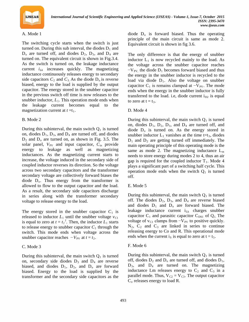
In CCM operation, next switching cycle starts before magnetizing current of transformer reaches zero. There are eight operating modes in the CCM operation. Typical voltage and current waveforms of proposed converter under CCM operation is shown in Fig 2. Current through and voltage across all the elements for each of the eight switching stages are plotted.
Fig 2. Typical voltage and current waveforms of the proposed DC–DC converter under CCM operation.
Fig 1. Proposed DC-DC converter
International Journal of Scientific Engineering and Applied Science (IJSEAS) - Volume-1, Issue-7, October 2015 ISSN: 2395-3470
www.ijseas.com
493
A. Mode 1
The switching cycle starts when the switch is just turned on. During this sub interval, the diodes D1 and Do are turned off, and diodes D2, D3, and D4 are turned on. The equivalent circuit is shown in Fig.3.4. As the switch is turned on, the leakage inductance current iLk increases quickly. The magnetizing inductance continuously releases energy to secondary side capacitors C2 and C3. As the diode Do is reverse biased, energy to the load is supplied by the output capacitor. The energy stored in the snubber capacitor in the previous switch off time is now releases to the snubber inductor, L1. This operation mode ends when the leakage current becomes equal to the magnetization current at t =t1.
B. Mode 2
During this subinterval, the main switch Q1 is turned on, diodes D1, D3, and D4 are turned off, and diodes D2 and Do are turned on, as shown in Fig. 3.5. The solar panel, VPV and input capacitor, C in provide energy to leakage as well as magnetizing inductances. As the magnetizing current starts to increase, the voltage induced in the secondary side of coupled inductor reverses its direction. So the voltage across two secondary capacitors and the transformer secondary voltage are collectively forward biases the diode Do. Thus energy from the transformer is allowed to flow to the output capacitor and the load. As a result, the secondary side capacitors discharge in series along with the transformer secondary voltage to release energy to the load. The energy stored in the snubber capacitor C1 is released to inductor L1 until the snubber voltage vC1 is equal to zero at t = t1
1. Then, the inductor L1 starts to release energy to snubber capacitor C1 through the switch. This mode ends when voltage across the snubber capacitor reaches −VPV at t = t2.
C. Mode 3
During this subinterval, the main switch Q1 is turned on, secondary side diodes D3 and D4 are reverse biased, and diodes D1, D2, and Do are forward biased. Energy to the load is supplied by the transformer and the secondary side capacitors as the
diode Do is forward biased. Thus the operating principle of the main circuit is same as mode 2. Equivalent circuit is shown in fig 3.6. The only difference is that the energy of snubber inductor L1 is now recycled mainly to the load. As the voltage across the snubber capacitor reaches −VPV, the diode D1 becomes forward biased and thus the energy in the snubber inductor is recycled to the load via diode D1. Also the voltage on snubber capacitor C1 is remains clamped at −VPV. The mode ends when the energy in the snubber inductor is fully transferred to the load. i.e, diode current iD2 is equal to zero at t = t3.
D. Mode 4
During this subinterval, the main switch Q1 is turned on, diodes D1, D2, D3, and D4 are turned off, and diode Do is turned on. As the energy stored in snubber inductor L1 vanishes at the time t=t3, diodes D1 and D2 are getting turned off immediately. The main operating principle of this operating mode is the same as mode 2. The magnetizing inductance Lm needs to store energy during modes 2 to 4, thus an air gap is required for the coupled inductor T1. Mode 4 plays a significant part of a switching half cycle. This operation mode ends when the switch Q1 is turned off.
E. Mode 5
During this subinterval, the main switch Q1 is turned off. The diodes D2, D3, and D4 are reverse biased and diodes D1 and Do are forward biased. The leakage inductance current iLk charges snubber capacitor C1 and parasitic capacitor CDS1 of Q1. The voltage of vC1 clamps from −VPV to positive quickly. N2, C2 and C3 are linked in series to continue releasing energy to Co and R. This operational mode ends when the current iS is equal to zero at t = t5.
F. Mode 6
During this subinterval, the main switch Q1 is turned off, diodes D2 and Do are turned off, and diodes D1, D3, and D4 are turned on. The magnetizing inductance Lm releases energy to C2 and C3 in a parallel mode. Thus, VC2 = VC3. The output capacitor Co releases energy to load R.
International Journal of Scientific Engineering and Applied Science (IJSEAS) - Volume-1, Issue-7, October 2015 ISSN: 2395-3470
www.ijseas.com
494
The leakage inductance current, iLk flows through D1 Fig 3. Equivalent circuits of the proposed dc–dc converter during one switching cycle under CCM operation: (a) Mode 1, (b) mode 2, (c) mode 3, (d) mode 4, (e) mode 5, (f) mode 6, (g) mode 7, and (h) mode 8.

International Journal of Scientific Engineering and Applied Science (IJSEAS) - Volume-1, Issue-7, October 2015 ISSN: 2395-3470
www.ijseas.com
495
The leakage inductance current, iLk flows through D1 to charge snubber capacitor C1. At that time the voltage of main switch Q1 is clamped at VPV + VC1. So the voltage across the switch will be nearly twice the input supply voltage. The energy in the leakage inductance is fully transferred to the snubber capacitor in this mode. This operation mode ends when the current through the snubber diode iD1 becomes zero at t = t6. It means the energy transfer from the leakage inductance to the snubber capacitor is completed.
G. Mode 7
During this subinterval, the main switch Q1 and diodes D1 and Do are turned off. But the diodes D2, D3, and D4 are turned on. The magnetizing inductance Lm releases energy to capacitors C2 and C3 continuously and charges them in parallel mode. The output Capacitor Co still releases energy to the load R. The trapped energy in the leakage inductance is restored back into the source during this mode. Because the voltage across snubber capacitor, VC1 is higher than VPV −VLk + VC2/n, the energy stored in C1 is released through D2 and T1 to source VPV, Cin, and N2. Therefore, the leakage energy is recycled back to the source efficiently. This operation mode ends when the voltage relations become VL1 + VC1 ≤ VPV −VLk + VC2/n at t = t7. Thus the function of snubber circuit is completed and only the main circuit works after this mode.
H. Mode 8
During this subinterval, the main switch Q1 is turned off, diodes D1, D2, and Do are turned off, and diodes D3 and D4 are turned on. The voltage across Q1 is equal to VPV −vLk1 + vC2/n, and the voltages across C2 and C3 are nearly nVPV D/(1−D). The magnetizing inductance Lm releases energy to C2 and C3. Co releases energy to R. This mode ends when the main switch Q1 is turned on at t = t8.
2.2 Discontinuous Conduction Mode of Operation
In DCM operation, the magnetizing current of transformer will be discontinuous. ie, next switching
cycle starts after the magnetizing current reaches zero. There are eight operating modes in the DCM operation. Typical voltage and current waveforms of proposed converter under CCM operation is shown in Fig 4.
Fig 4. Typical voltage and current waveforms of the proposed DC–DC converter under DCM operation. A. Mode a
During this subinterval, the main switch Q1 is turned on. The diodes D1, D3, and D4 are reverse biased, while the diodes D2 and Do are forward biased. The energy of snubber capacitor C1 is released to inductor L1. This operating mode ends when iC1 and iD2 are equal to zero at t = t1.
B. Mode b
International Journal of Scientific Engineering and Applied Science (IJSEAS) - Volume-1, Issue-7, October 2015 ISSN: 2395-3470
www.ijseas.com
496
During this subinterval, the main switch Q1 is turned on, diodes D1, D2, D3, and D4 are reverse biased, and diode Do is forward biased. The voltage of the solar panel VPV and the input capacitor C in transfer energy through coupled inductor T1 to secondary winding N2 with high step-up capacitors C2 and C3 and then through output diode Do to transfer energy to output capacitor Co and output load R. Part of the energy from the voltage of the solar panel VPV and the input capacitor Cin is stored in primary magnetizing inductance Lm. The mode ends when the main switch Q1 is turned off at t = t2.
C. Mode c
During this subinterval, the main switch Q1 is turned off, diodes D2, D3, and D4 are turned off, and diodes D1 and Do are turned on. The leakage inductance current iLk charges snubber capacitor C1 and parasitic capacitor CDS1 of Q1, and the voltage of vC1 clamps from −VPV to positive quickly. N2, C2, and C3 are linked in series to continue releasing energy to Co and R. This operational mode ends when the current iS is equal to zero at t = t5.
D. Mode d
During this subinterval, the main switch Q1 is turned off, diodes D2 and Do are turned off, and diodes D1, D3, and D4 are turned on. The magnetizing inductance Lm releases energy to C2 and C3 in a parallel mode. Thus, vC2 = vC3. Co releases energy to R. iLk flows through D1 to charge snubber capacitor C1. Thus, the voltage of main switch Q1 is clamped at VPV + vC1. This mode ends when snubber diode current iD1 is equal to zero at t = t6.
E. Mode e
During this subinterval, the main switch Q1 is turned off, diodes D1, D2, and Do are reverse biased, and diodes D3 and D4 are forward biased. The magnetizing energy Lm is transferred to C2, as well as C3 in a parallel way. The energy stored in Co is transferred to load R. The mode ends when the primary magnetizing current iLm reaches zero at time t = t5.
F. Mode f
During this subinterval, the main switch Q1 is turned off, diodes D1, D3, D4, and Do are reverse biased, and diode D2 is forward biased. The energy of snubber capacitor C1 and inductor L1 is released to the voltage of the solar panel VPV and the input capacitor C in, and the energy is transferred from Co to R. The mode ends when iC1 and iD2 are equal to zero at t = t6.
G. Mode g
During this subinterval, both the main switch and diodes are switched off, and the primary magnetizing inductance voltage and current are both zero. The energy is also transferred from Co to R. The voltage waveforms of vQ1 have some oscillations caused by the parasitic capacitor CDS1 of switch Q1. The primary magnetizing inductance Lm and the leakage inductance Lk are formed in resonance when iLm and iLk are equal to zero. The mode ends when the main switch Q1 is turned on at t = t7.
4. Theoretical Analysis
The theoretical analysis is done for a fixed duty cycle considering one switching period and steady state analysis in continuous conduction mode. To simplify the analysis of proposed converter, the following assumptions are made during one switching cycle: 1. The main switch Q1 and all the diodes are
regarded as ideal components; only the parasitic capacitor CDS1 of the main switch Q1 is considered.
2. Capacitors C in, C2, C3, and Co are sufficiently large that VPV, VC2, VC3, and Vo are regarded as constant values.
3. The turns ratio of the coupled inductor T1 is n = N2/N1, and the magnetizing inductance Lm and leakage inductance Lk1 of the coupled inductor T1 are considered in the analysis.
Because the magnetizing inductance Lm is much larger than the leakage inductance Lk1, the time intervals 1,2,3,5,6 and 7 are very short as compared to one switching period. Thus, only operating modes 4 and 8 are discussed.

International Journal of Scientific Engineering and Applied Science (IJSEAS) - Volume-1, Issue-7, October 2015 ISSN: 2395-3470
www.ijseas.com
497
The primary side magnetizing inductance voltage VLm, capacitor voltages VC1 and VC2 can be expressed as,
(1)
(2)
During mode 8 of operation, flux density, B is decreased by ∆B and the magnetizing inductance voltage VLm can be expressed as,
(3) According to the principle of volt–second balance of the primary side magnetizing inductance Lm, the voltage gain can be expressed as,
(4)
Substituting (2) in (4) yields the total voltage gain as,
(5) The voltage and current stresses of the main switch Q1 and diodes D3, D4, and Do can be expressed as
(6)
(7)
Average currents through Q1 is,
(8)
Average currents through diodes D3,D4 and Do are,
(9)
The boundary-normalized magnetizing inductance time constant is defined as follows:
(10)
Solving (10), can be expressed as,
(11)
4.1 Calculation of Duty Cycle
Assume that the main switch voltage is clamped at 45 V with neglecting the effect of leakage inductance. From (6) duty ratio can be obtained by,
(12)
The duty ratio is obtained as 0.47.
4.2 Design of Coupled Inductor
Substituting the value of D in the equation (5) of voltage gain, transformer turns ratio, n is obtained as 3. By putting values of n and D in the equation (11) of magnetizing inductance time constant, 𝞽𝞽LB is obtained as 2.495x10⁻³. From equation (3.10), Lm is obtained as 25µH.
4.3 Calculation of C1
The energy stored in leakage inductance Lk1 during the switch-on period is completely released to the snubber capacitor C1 during the switch-off period. It can be explained as,
(13)
Where, iLk−max is the maximum leakage inductance current during the switch-on period, iLk−min is the minimum leakage inductance current during the switch-on period, vC1−max is the maximum snubber capacitor voltage, and vC1−min is the minimum snubber capacitor voltage.
4.4 Calculation of L1
If the maximum switch voltage spike VQ1 is assumed as 80 V by considering the effect of the leakage inductance, usually, the leakage inductance Lk is about 1% of Lm. Then, the snubber inductor L1 can be calculated as,
(14)

International Journal of Scientific Engineering and Applied Science (IJSEAS) - Volume-1, Issue-7, October 2015 ISSN: 2395-3470
www.ijseas.com
498
The snubber inductance L1 is obtained as 4.6 µH.
5. Simulink model and simulation results
This chapter gives simulation study for a prototype implemented with output rated power of 100W, giving an output dc voltage of 200V when an input voltage of 24V is given. The frequency at which the switch is operated is 50 kHz. The simulation is done for continuous conduction mode of operation. The parameters given to the circuit for obtaining an output voltage of 200V are listed below. A pulse generator with 47% pulse width and 50 kHz frequency is used to supply gate pulse to the MOSFET switch.
Table 1 Simulation parameters
Parameters Value
DC Input voltage (Vin) 24 V
Output power (Po) 100 W
Load resistance 400 Ω
Switching frequency (Fs) 50 kHz
Transformer turns ratio (n) 3
Duty ratio (D) 47 %
Magnetization inductance (Lm) 50 µH
Leakage inductance (Lk) 0.21 µH
Snubber capacitance (C1) 22 nF
Snubber inductance (L1) 4.6 µH
Output capacitor (Co) 2200 µF Secondary side capacitors (C1,C2) 100 µF
Fig 5.Open loop model of proposed converter
5.1 Simulation Result
The response of the proposed circuit can be analyzed from the simulation results. The switching pulse given to the switch Q1 is of 50 kHz frequency. The simulated waveform of pulse is shown in fig 6.
Fig 6. Pulse given to switch Q1
The simulated coupled inductor magnetization current and leakage current are shown in figures 7 and 8 respectively. As the switch Q1 is turned on (mode 1), coupled inductor magnetization current (ILm ) is decreased to its minimum value of 5A due to the rapid increase in the coupled inductor leakage current.
Fig.7 Magnetization current of coupled inductor

International Journal of Scientific Engineering and Applied Science (IJSEAS) - Volume-1, Issue-7, October 2015 ISSN: 2395-3470
www.ijseas.com
499
After mode 1, ILm increased linearly from 5A to 9.3A. Magnetization current reached its peak value at the end of mode 5. As the switch is turned off, ILm begins to decrease and it reaches its minimum value of 5A at the end of mode 1 of next switching cycle. It again increases as the mode 2 starts.
Fig.8 Leakage current of coupled inductor The coupled inductor leakage current (ILk) increased quickly as the switch Q1 is turned on and it reached a value of 6.5A at the end of mode 1 itself. As ILm starts to develop after the end of mode 1, the rise of ILk become sluggish and it reaches its maximum value of 13A at the end of mode 4, i.e just before the switch is turned off. When the switch is turned off, ILk falls rapidly and reaches zero at the end of mode 6. During mode 7, ILk just increased in the opposite direction and again falls to zero. During mode 8 of operation, leakage current is absolutely zero. Figure 9 shows the simulated waveforms of voltage across the switch Q1. When the switch is just turned on, voltage across it drops rapidly to zero and current through it rises quickly. During the switch ON period, voltage across the switch is 2 V, due to the internal resistance of the switch and current though it is 21.7 A.
Fig 9. Voltage across the switch Q1
Simulated waveforms of voltage across and current though the snubber capacitor C1 is shown in figures 10 and 11 respectively. When the switch is just turned off, the leakage inductance current, ILk charges snubber capacitor C1, so the current through C1 rises rapidly to 14 A and voltage develops across the capacitor. When the current becomes zero, the voltage reaches the maximum value 50 V. Then during mode 7, since energy in the snubber capacitor is released to the VPV, the capacitor voltage is decreased and it remains constant at 40 V till the switch is turned ON.
Fig.10 Voltage across the snubber capacitor C1
As the switch is turned ON, voltage across C1 decreases due to the release of energy to snubber inductor (L1). So the snubber capacitor current develops in reverse direction till VC1 becomes zero. As VC1 becomes zero, then L1 starts release energy to snubber capacitor, hence snubber voltage develops in reverse direction till VC1= -24 V.
Fig11. Current though the snubber capacitor C1.
The simulated waveforms of diode currents ID1 and ID2 are shown in fig 12 and 13 respectively. As the coupled inductor leakage current charges C1when the switch is just turned off, the diode D1 conducts and the charging current of 14A flows through diode D1. D1 is turned off as the leakage current falls to zero.

International Journal of Scientific Engineering and Applied Science (IJSEAS) - Volume-1, Issue-7, October 2015 ISSN: 2395-3470
www.ijseas.com
500
Diode D2 becomes forward biased in mode 7 because of the voltage VC1, and thus current flows through D2 so as to recycle leakage energy to VPV. Diode D2 conducts in mode 1 to 3 so as to charge and discharge between snubber capacitor and snubber inductor. The peak value of current through diode D2 is 2.2A.
Fig.12 Current through diode D1
Fig.13 Current through diode D2
Simulated waveforms of secondary current of coupled inductor (Is) and current through diode D3 is shown in figures 14 and 15 respectively. Secondary current develops quickly as the switch is turned on and reaches a value of 3A and the current through the diodes D3 and D4 drops to zero.
Fig 14. Secondary current of coupled inductor
Fig 15. Current through diode D3
After mode 1, coupled inductor secondary current remains almost constant for the switch on period. At this time diodes D3 and D4 are reverse biased and the current is flowing directly to the load and output capacitor. When the switch is turned off, current Is drops to zero. As ILm starts decaying, the direction of Is gets reversed. During mode 7, as the leakage energy is also transferred to secondary, there is an increase in Is for the duration of mode 7 (i.e current reaches -5A). At the end of the switch off time, secondary current reaches its minimum value of 3.5A in reverse direction.
The simulated waveform of current through diode Do is shown below. No current flows through diode Do during mode 1 of operation, because it is reverse biased due to the voltage of output capacitor Co. Diode current develops just after the end of mode 1 as the VC1 and VC2 becomes more than VCo.
Fig.16. Current through diode Do
The output voltage waveform is shown in the fig 17. The output voltage waveform was well settled at 200V in 0.02 seconds. There exists no overshoots before settling the voltage waveform and the output voltage waveform is free from ripples. The load
International Journal of Scientific Engineering and Applied Science (IJSEAS) - Volume-1, Issue-7, October 2015 ISSN: 2395-3470
www.ijseas.com
501
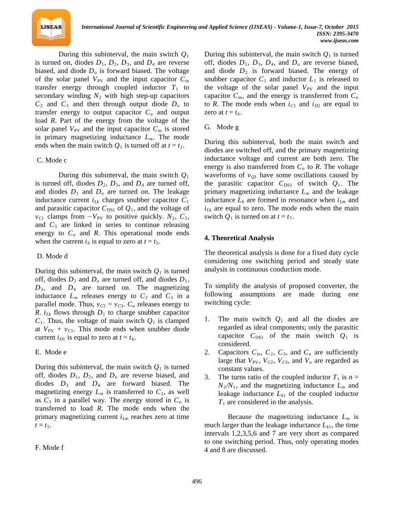
current also follows the output voltage waveform, as the load was resistive load.
Fig.17. Simulated waveform of output voltage
4.3 Closed Loop Simulink Model of Proposed
Converter
Fig.18 Closed loop model of the converter
The closed loop regulation is necessary to achieve good dynamic response under varying plant parameter condition. Proportional and Integral controller is used here. PI controller is used normally in many applications because of its simplicity.
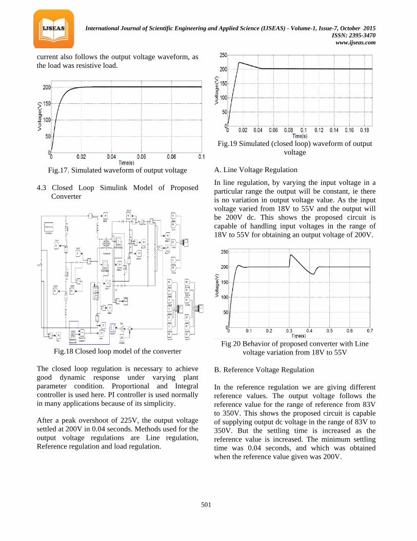
After a peak overshoot of 225V, the output voltage settled at 200V in 0.04 seconds. Methods used for the output voltage regulations are Line regulation, Reference regulation and load regulation.
Fig.19 Simulated (closed loop) waveform of output
voltage A. Line Voltage Regulation
In line regulation, by varying the input voltage in a particular range the output will be constant, ie there is no variation in output voltage value. As the input voltage varied from 18V to 55V and the output will be 200V dc. This shows the proposed circuit is capable of handling input voltages in the range of 18V to 55V for obtaining an output voltage of 200V.
Fig 20 Behavior of proposed converter with Line
voltage variation from 18V to 55V
B. Reference Voltage Regulation In the reference regulation we are giving different reference values. The output voltage follows the reference value for the range of reference from 83V to 350V. This shows the proposed circuit is capable of supplying output dc voltage in the range of 83V to 350V. But the settling time is increased as the reference value is increased. The minimum settling time was 0.04 seconds, and which was obtained when the reference value given was 200V.

International Journal of Scientific Engineering and Applied Science (IJSEAS) - Volume-1, Issue-7, October 2015 ISSN: 2395-3470
www.ijseas.com
502
Fig.21 Behavior of proposed converter with reference
voltage value 350V
C. Load regulation In the load regulation, the proposed converter is connected across different loads and the circuit maintains a constant output voltage of 200V. First, an output load of 200W is connected. After 0.3 seconds, the load is changed as 500W by connecting a parallel resistance. Again the load is changed to 800W after 0.3 seconds. That is the load is changed from 200W to 800W in three steps. Fig 4.21 proves that the output voltage remains constant at 200V for any change in load between 200W to 800W.
Fig.22 Behavior of proposed converter with load
variation from 200W to 800W
The simulation of the converter and its closed loop control has been carried out .The results shows that the voltage boosting is carried out effectively. The efficiency is also high. Also the closed loop implementation of proposed converter works well as it performs very good line regulation and load
regulation. It maintains output voltage level at constant 200V for a wide range of changes in input voltage (i.e, 18V to 55V). Also output voltage remains at constant 200V for change in load from 200W to 800W. The reference regulation behaviour is also excellent as it gives the correct reference value as output for a reference value up to 350V.
6. Experimental Setup of the Converter
This chapter describes the verification of the proposed high step up DC-DC converter with an experimental set up. The hardware setup is designed and created for converting a dc voltage of 12V to 100V as per the table 1. Hardware set up consists of power circuit, control circuit, gate driving circuit and control circuit power supply. The schematic diagram of the hardware setup is shown in fig 23.
Fig.23 Schematic Diagram of Hardware Setup 6.1 Controller Circuit Realization The IC employed in realizing the control circuit is dsPIC 30F2010. dsPIC 30F2010 is a 28 pin IC which should be supplied with a regulated dc supply of 3.3V. This IC consists of an internal ADC and three inbuilt PWM generators. Output from the feedback circuit is given as input to the ADC pin of dsPIC. The output pulse from the PWM generators is used for adjusting the duty cycle for switching the converter as per the level. The pin out diagram of dsPIC30F2010 is shown in fig 24. The dsPIC is programmed for obtaining a switching pulse of 50kHz which is needed for the MOSFET switch.

International Journal of Scientific Engineering and Applied Science (IJSEAS) - Volume-1, Issue-7, October 2015 ISSN: 2395-3470
www.ijseas.com
503
Fig.24. Pin out diagram of dsPIC 30F2010
In the control circuit of dsPIC IC, pins 8, 19 and 27 are connected to ground. Pin 28, 20 and 13 connected to source of 3.3V. There are totally 6 pins for getting pulses. The Pin 25 and 26 is the pin meant to give pulses to drive the Converter. Pin 3 is meant for the feedback IC 4N25 input to dsPIC. Between the 9th and 10th pin we have the connection of 4 MHz crystal oscillator, which gives the clock pulses for the operation of IC. The reset switch is connected at pin 1.
Fig.25 Control circuit with dsPIC 30F2010
The controller section consists of IC dsPIC 30f2010, Crystal oscillator, adapter, regulator, capacitors, resistors, etc. The crystal oscillator is of 8MHz. An adapter is needed for giving the 12V Supply for TLP250 IC and 3.3 V supply for the PIC. Two capacitors of 22pf is needed for the working of crystal oscillator. The coupling capacitors used are of 0.1 microfarad. The hardware implementation of control section of the proposed converter with feedback circuit is shown in fig. 5.3.
6.2 Feedback Circuit
The feedback circuit in proposed technique is achieved by IC 4N25, which is a 6 pin opto isolator transistor. The feedback circuit diagram is shown in Fig.5.4. Pin 1 and 2 are the input ports of feedback circuit. Pin 4 is the output pin which should be connected to the 3rd pin of dsPIC IC, as 3rd pin is the ADC port of dsPIC. Here in the feedback circuit, we take the voltage feedback from the power circuit output for properly implementing the algorithm in dsPIC. The feedback circuit is connected with power circuit via a current limiting resistor, in order to limit current through feedback circuit when the load is applied.
Fig.26 Feedback circuit using 4N25
6.3 MOSFET Gate Drive Circuit In this work, TLP250 driver is employed for driving the MOSFET gate. Fig. 5.5 shows a typical MOSFET gate driver circuit using TLP250 IC. The gate driver is is an integrated chip transistor driver with optical isolation which accepts low power input from a controller IC and produces a high current output for driving the gate of high power transistors such as IGBT and power MOSFET. Like any driver, it has an input stage, an output stage and a power supply connection. The input drive signal from dsPIC is connected to the 2nd pin of TLP250 IC, that dictates the output state which is referenced to signal ground.
International Journal of Scientific Engineering and Applied Science (IJSEAS) - Volume-1, Issue-7, October 2015 ISSN: 2395-3470
www.ijseas.com
504
Fig.27 MOSFET gate drive circuit using TLP250
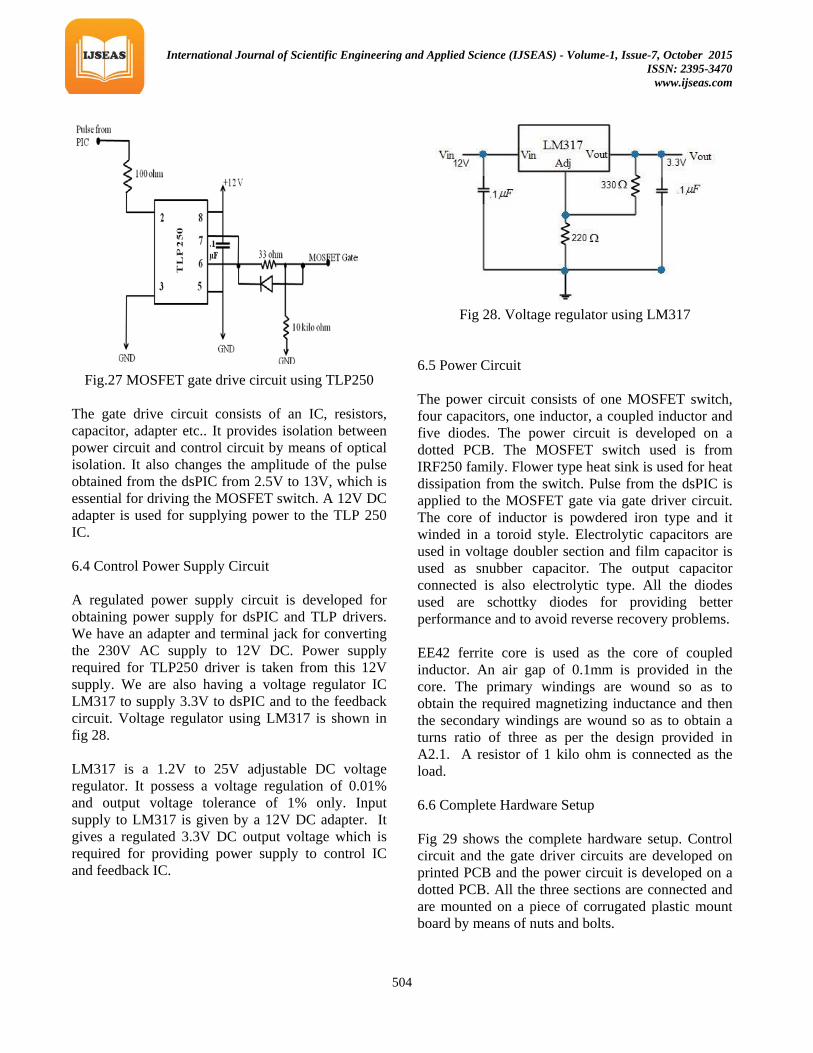
The gate drive circuit consists of an IC, resistors, capacitor, adapter etc.. It provides isolation between power circuit and control circuit by means of optical isolation. It also changes the amplitude of the pulse obtained from the dsPIC from 2.5V to 13V, which is essential for driving the MOSFET switch. A 12V DC adapter is used for supplying power to the TLP 250 IC. 6.4 Control Power Supply Circuit A regulated power supply circuit is developed for obtaining power supply for dsPIC and TLP drivers. We have an adapter and terminal jack for converting the 230V AC supply to 12V DC. Power supply required for TLP250 driver is taken from this 12V supply. We are also having a voltage regulator IC LM317 to supply 3.3V to dsPIC and to the feedback circuit. Voltage regulator using LM317 is shown in fig 28. LM317 is a 1.2V to 25V adjustable DC voltage regulator. It possess a voltage regulation of 0.01% and output voltage tolerance of 1% only. Input supply to LM317 is given by a 12V DC adapter. It gives a regulated 3.3V DC output voltage which is required for providing power supply to control IC and feedback IC.
Fig 28. Voltage regulator using LM317
6.5 Power Circuit The power circuit consists of one MOSFET switch, four capacitors, one inductor, a coupled inductor and five diodes. The power circuit is developed on a dotted PCB. The MOSFET switch used is from IRF250 family. Flower type heat sink is used for heat dissipation from the switch. Pulse from the dsPIC is applied to the MOSFET gate via gate driver circuit. The core of inductor is powdered iron type and it winded in a toroid style. Electrolytic capacitors are used in voltage doubler section and film capacitor is used as snubber capacitor. The output capacitor connected is also electrolytic type. All the diodes used are schottky diodes for providing better performance and to avoid reverse recovery problems. EE42 ferrite core is used as the core of coupled inductor. An air gap of 0.1mm is provided in the core. The primary windings are wound so as to obtain the required magnetizing inductance and then the secondary windings are wound so as to obtain a turns ratio of three as per the design provided in A2.1. A resistor of 1 kilo ohm is connected as the load. 6.6 Complete Hardware Setup Fig 29 shows the complete hardware setup. Control circuit and the gate driver circuits are developed on printed PCB and the power circuit is developed on a dotted PCB. All the three sections are connected and are mounted on a piece of corrugated plastic mount board by means of nuts and bolts.

International Journal of Scientific Engineering and Applied Science (IJSEAS) - Volume-1, Issue-7, October 2015 ISSN: 2395-3470
www.ijseas.com
505
Fig.29 Complete hardware setup
6.7 Hardware Results The hardware setup was implemented as per the parameters tabulated in table1. When 12V DC supply is given to the proposed circuit as input, the output voltage obtained was 100V DC. The prototype circuit maintains its constant terminal voltage of 100V for an input voltage range of 10V to 16V. Also maintains a constant output voltage of 100V for different load conditions. i.e., the closed loop control of hardware setup is completed and verified. All the waveforms are saved in a digital storage oscilloscope (DSO). The hardware output waveform of the switching pulse given to the MOSFET switch is shown in figure 5.8. The frequency of switching pulse is 50 kHz and the amplitude of the pulse given to the switch is 13V. The designed duty cycle of the switching pulse was 0.47. But the duty ratio of the switching pulse under closed loop control is obtained as 0.493. Five switching cycles are shown in the figure. The low amplitude of the switching pulse obtained from the dsPIC is converted to 13V by the gate driver circuit. The output pulse from gate driver circuit is shown in figure 30.
Fig 30 Switching pulse given to MOSFET switch
The magnetization current waveform of the coupled inductor is shown in the figure 31.
Fig.31 Magnetization current of coupled inductor
The magnetization current increases to an upper limit and then it decays to the lower limit in one switching cycle. The magnetization current is increased and it reaches up to 5A at the end of switch on time and it is decreased to 0.7A at the end of one switching cycle. The magnetization current never reached zero, thus the circuit is operating in continuous conduction mode. The DSO image of output voltage and current waveforms are shown in fig 5.10. Same as designed, the output voltage across the load is obtained as 100V. The output current through the load is obtained as 234mA.

International Journal of Scientific Engineering and Applied Science (IJSEAS) - Volume-1, Issue-7, October 2015 ISSN: 2395-3470
www.ijseas.com
506
Fig 32. Output voltage and output current
The DSO image of voltage across the power switch is shown in fig 33. The voltage across the switch during switch off time is obtained as 26V. When the switch is just turned on, voltage across it drops rapidly to zero and current through it rises quickly. During the switch on period, voltage across the switch is nearly 2V, due to the internal resistance of the switch. When the switch is turned off, current falls rapidly and becomes zero at the end of mode 6. At the same time voltage across it shoots to 50V and then suddenly decreased to 26V and it is maintained as long as the switch is in on condition. Also the duty ratio can be easily predicted from the switch voltage.
Fig.33 Voltage across the switch
Fig 34 shows the waveform of voltage across the snubber capacitor. The voltage reverses its direction for each on-off half cycle. Also it can be seen that the
capacitor keeps constant voltage across it during 4th and 8th mode of operation, because at that time, only the main circuit is in operation.
Fig.34 Voltage across snubber capacitor
6.8 Comparison between Hardware Results and
Simulation Results
Table 2 Comparison between hardware results and simulation results
In order to validate the hardware results, the proposed converter circuit is again simulated with

International Journal of Scientific Engineering and Applied Science (IJSEAS) - Volume-1, Issue-7, October 2015 ISSN: 2395-3470
www.ijseas.com
507
same specifications as that of hardware design (Table.5.1). i.e MATLAB simulation of closed loop implementation of the proposed converter with 12V DC input is done. The simulation results are compared with the hardware results. Hardware waveforms and the simulation waveforms reveals that the hardware results matching the simulation results.
The hardware results of the proposed system are described in this chapter. The control part of the hardware circuit is implemented with the help of dsPIC30F2010. The power circuit, control circuit and the gate driver circuit are implemented on separate circuit boards. The output waveforms are viewed with the help of a digital storage oscilloscope. The prototype output waveforms obtained from the DSO is similar to that of simulation results. These results are also analyzed in this chapter. 7. Summary and Conclusion
This project presented a new topology for isolated DC–DC converter. The proposed converter realizes high step up voltage gain without incurring a high coupled inductor turns ratio. From the detailed simulation and experimental analysis, it is clear that the presented converter has the following advantages. 1. A coupled inductor and a voltage doubler circuit
are employed in the presented converter. The coupled inductor turns ratio is 3. The voltage doubler doubles the output voltage. Hence it achieves high step- up voltage gain.
2. The main problem faced by isolated converters is its low efficiency due to the energy wastage in the coupled inductor leakage reactance. The snubber circuit effectively restores the leakage energy to the source. Thus the energy in the leakage inductor of the coupled inductor is recycled and thus the converter efficiency gets improved.
3. A voltage doubler is employed at the secondary side of the coupled inductor, which rectifies and doubles the output voltage. As the voltage doubler circuit is employed, the size of the coupled inductor can be reduced.
4. An LC snubber circuit is employed in order to protect the power switch from voltage spikes due to fast switching. Also there is no energy dissipation takes place as the snubber used is of LC circuit instead of RC circuit. By the use of snubber circuit, the voltage stress on the power switch is reduced one third. So a power switch with low voltage stress and low ON-resistance (Ron) can be selected.
5. The low voltage stress of the output diode enables the selection of a low forward voltage diode, it also improves the efficiency.
As the terminal voltage of solar power modules are very low, a DC-DC converter is very essential for the effective power utilization. Also non-isolated converters cannot satisfy the requirements of galvanic isolation standards. Thus an isolated DC-DC converter finds its application in various fields. In isolated converters, the presented converter possesses

International Journal of Scientific Engineering and Applied Science (IJSEAS) - Volume-1, Issue-7, October 2015 ISSN: 2395-3470
www.ijseas.com
508
high voltage gain and high conversion efficiency with low voltage stress. 7.1 Future Scope In future the converter can be redesigned for high power applications by implementing inductors instead of capacitors in the voltage doubler circuit. If the voltage doubler using inductors is implemented, the converter can supply high power loads. Also active switches can be used instead of diodes. The converter voltage gain can be improved much more without extreme switch duty cycle by using a three winding coupled inductor, which in addition enhancing the utility rate of magnetic core. Also the control scheme for controlling the switch can be implemented by using fuzzy logic.
REFERENCES
[1] F. Zhang, Lei Du, and F. Z. Peng. “A new design method for high-power high-efficiency switched-capacitor dc–dc converters,” IEEE Trans. Power Electron., vol.23 , no.2 , pp. 832-840, Mar. 2008.
[2] A. Fardoun and E. H. Ismail, “Ultra step-up DC–DC converter with reduced switch stress,” IEEE Trans. Ind. Appl., vol. 46, no. 5, pp. 2025–2034, Sep./Oct. 2010.
[3] K. C. Tseng and T. J. Liang, “Analysis of integrated boost–flyback stepup converter,” Proc. Inst. Elect. Eng. Elect. Power Appl., vol. 152, no. 2, pp. 217–225, Mar. 2005.
[4] O. Abutbul, A. Gherlitz, Y. Berkovich, and A. Ioinovici, “Step-up switching-mode converter with high voltage gain using a switchedcapacitor circuit,” IEEE Trans. Circuits Syst. I, Fundam. Theory Appl., vol. 50, no. 8, pp. 1098–1102, Aug. 2003.
[5] L. S. Yang, T. J. Liang, H. C. Lee, and J. F. Chen, “Novel high step-up DC–DC converter with coupled inductor and voltage-doubler circuits,” IEEE Trans. Ind. Electron., vol. 58, no. 9, pp. 4196–4206, Sep. 2011.
[6] T. F. Wu, Y. S. Lai, J. C. Hung, and Y. M. Chen, “Boost converter with coupled inductors and buck–boost type of Active clamp,” IEEE Trans. Ind. Electron., vol. 55, no. 1, pp. 154–162, Jan. 2008.
[7] J. W. Baek, M. H. Ryoo, T. J. Kim, D. W. Yoo, and J. S. Kim, “Highboost converter using voltage multiplier,” in Proc. IEEE IECON, 2005,pp. 567–572.
[8] J. M. Shen, H. L. Jou, and J. C. Wu, “Novel transformer less grid connected power converter with negative grounding for photovoltaic generation system,” IEEE Trans. Power Electron., vol. 27, no. 4, pp. 1818–1829, Apr. 2012.
[9] L. Zhang, K. Sun, L. Feng, and H. Ge, “A modular grid-connected photovoltaic generation system based on DC bus,” IEEE Trans. Power Electron., vol. 26, no. 2, pp. 523–531, Feb. 2011.
[10] T. Suntio, J. Leppaaho, and J. Huusari, “Issues on solar-generator interfacing with voltage-fed converter,” in Proc. IEEE IECON, 2009, pp. 595–600.
[11] J. Leppaaho and T. Suntio, “Dynamic characteristics of current-fed superbuck converter,” IEEE Trans. Power Electron., vol. 26, no. 1, pp. 200–209, Jan. 2011.
[12] C. Rodriguez and G. A. J. Amaratunga, “Long-lifetime power inverter for photovoltaic AC modules,” IEEE Trans. Ind. Electron., vol. 55, no. 7, pp. 2593–2601, Jul. 2008.
[13] Q. Li and P. Wolfs, “A review of the single phase photovoltaic module integrated converter topologies with three different DC link configurations,” IEEE Trans. Power Electron., vol. 23, no. 3, pp. 1320–1333, May 2008.
[14] D. Sera, R. Teodorescu, J. Hantschel, and M. Knoll, “Optimized maximum power point tracker for fast-changing environmental conditions,” IEEE Trans. Ind. Electron., vol. 55, no. 7, pp. 2629–2637, Jul. 2008.
International Journal of Scientific Engineering and Applied Science (IJSEAS) - Volume-1, Issue-7, October 2015 ISSN: 2395-3470
www.ijseas.com
509
[15] T. Mishima, Y. Takeuchi, and M. Nakaoka, “A new high step-up voltage ratio soft switching PWM boost DC–DC power converter with edge resonant switched capacitor modular,” in Proc. IEEE EPE, 2011, pp. 1–10.
[16] CM. Young, M. H. Chen, T. A. Chang, and C. C. Ko, “Transformerless high step-up DC–DC converter with Cockcroft–Walton voltage multiplier,” in Proc. IEEE IEIEA, 2011, pp. 1599–1604.
[17] M. Prudente, L. L. Pfitscher, G. Emmendoerfer, E. F. Romaneli, and R. Gules, “Voltage multiplier cells applied to non-isolated DC–DC converters,” IEEE Trans. Power Electron., vol. 23, no. 2, pp. 871–887, Mar. 2008.
[18] F. L. Tofoli, D. D. S. Oliveira, J. R. P. T. Bascope, and Y. J. A. Alcazar, “Novel nonisolated high-voltage gain DC–DC converters based on 3SSC and VMC,” IEEE Trans. Power Electron., vol. 27, no. 9, pp. 3897–3907, Sep. 2012.
[19] K. B. Park, H. W. Seong, H. S. Kim, G. W. Moon, and M. J. Youn, “Integrated boost–sepic converter for high step-up applications,” in Proc. IEEE PESC, 2008, pp. 944–950.
[20] A. Nami, F. Zare, A. Ghosh, and F. Blaabjerg, “A hybrid cascade converter topology with series-connected symmetrical and asymmetrical diodeclamped H-bridge cells,” IEEE Trans. Power Electron., vol. 26, no. 1, pp. 51–65, Jan. 2011.
[21] K. J. Lee, B. G. Park, R. Y. Kim, and D. S. Hyun, “Nonisolated ZVT twoinductor boost converter with a single resonant inductor for high step-up applications,” IEEE Trans. Power Electron., vol. 27, no. 4, pp. 1966–1973, Apr. 2012.
[22] S. K. Changchien, T. J. Liang, J. F. Chen, and L. S. Yang, “Novel high step-up DC–DC converter for fuel cell energy conversion system,” IEEE Trans. Ind. Electron., vol. 57, no. 6, pp. 2007–2017, Jun. 2010.
[23] S. Dwari and L. Parsa, “An efficient high-step-up interleaved DC–DC converter with a common active clamp,” IEEE Trans. Power Electron., vol. 26, no. 1, pp. 66–78, Jan. 2011.
[24] S. M. Chen, T. J. Liang, L. S. Yang, and J. F. Chen, “A boost converter with multiplier and coupled inductor for AC module applications,” IEEE Trans. Ind. Electron., vol. 60, no. 4, pp. 1503–1511, Apr. 2013.
[25] B. R. Lin, J. Y. Dong, and J. J. Chen, “Analysis and implementation of a ZVS/ZCS DC–DC switching converter with voltage step-up,” IEEE Trans. Ind. Electron., vol. 58, no. 7, pp. 2962–2971, Jul. 2011.
APPENDIX-II
A2.1 Winding Design of Coupled Inductor
Winding design of acoupled inductor consist of the following steps:
1. Calculation of number of turns: We know that, the emf equation,
From this equation we get:
Where, dI=ip=ΔiLM=Inductor peak current = 9A ΔB=0.3T to 0.6T for avoiding the saturation 2. Calculation of air gap: We have,
Magnetising inductance, Therefore air gap length is given by
3. Selection of core:
Core is selected considering power handling capability and for occupying coil turns. Core used is EE42 ferrite core, having le= 9.7 cm and Ae=180mm2
.
4. Selection of coil for winding Coil selection is in accordance with the
current needed to carry. For the coupled inductor having Lm=50 µH,

International Journal of Scientific Engineering and Applied Science (IJSEAS) - Volume-1, Issue-7, October 2015 ISSN: 2395-3470
www.ijseas.com
510
Peak current of inductor can be dI=Ip= 1.5(safety factor) x peak current
= 1.5 x 9 = 13.5 A
So number of turns in primary = 13 Air gap length =0.16mm
A2.2 Program for Controlling the Proposed DC-DC Converter
//ADCON2 Register //Set up A/D for interrupting after 2 samples get filled in the buffer //Set up to sample on 2 S/H amplifiers - CH0 and CH1 //All other bits to their default state ADCON2bits.SMPI = 0; ADCON2bits.CHPS = 1; //selected ch0 & 1 ADCON2bits.VCFG = 0; //used AVdd and AVss as references //ADCON3 Register ADCON3bits.SAMC = 1; ADCON3bits.ADCS = 15; //4 //ADCHS Register ADCHS = 0x0024; //selected ch0 for AN4 and ch1 for AN3 //ADCSSL Register ADCSSL = 0x0000; //ADPCFG Register ADPCFG = 0xFFFF; ADPCFGbits.PCFG3 = 0; ADPCFGbits.PCFG4 = 0; //Clear the A/D interrupt flag bit IFS0bits.ADIF = 0; //Set the A/D interrupt enable bit IEC0bits.ADIE = 1; //Turn on the A/D converter ADCON1bits.ADON = 1; } void __attribute__((__interrupt__)) _ADCInterrupt(void) { ADC_RESULT = ADCBUF0; IFS0bits.ADIF = 0;
} int main() { ADC_Init(); Init_PWM_1(50000,70); while(1); return (0); }
APPENDIX-III
A3.1 PCB Layout of Control Circuit
A3.2 PCB Layout of Driver Circuit

International Journal of Scientific Engineering and Applied Science (IJSEAS) - Volume-1, Issue-7, October 2015 ISSN: 2395-3470
www.ijseas.com
511
A3.3 Schematic Diagram and Pin Configuration of TLP250 IC
A3.4 IRF250N Power MOSFET
A3.5 EE42 Ferrite Core
NABEEL P received the B.Tech. degree in electrical engineering from Kannur University, Kerala, India in 2013 and is currently pursuing the M.Tech degree at
M.E.A. Engineering College under Calicut University, Kerala. NAYAS QUDRATHULLA P. P received the B.Tech. degree in electrical engineering from Calicut University, Kerala, India in 2011, received the M.Tech degree in Power Electronics and Drives from Anna University and is currently working as Assistant Professor in M.E.A Engnering Colege, Perintalmanna.