Embed Size (px)
Citation preview

Eighth International Symposium on Space Terahertz Technology, Harvard University, March 1997
An Investigation of the Input Impedance of aMicrostrip Probe in Waveguide.
S. Withington and G. Yassin
Department of Physics,University of Cambridge,
Madingley Rd, Cambridge.
Abstract
We derive an expression for the input impedance of a one-sided mi-crostrip probe in waveguide. By "one-sided" we mean an insulatedprobe that extends only part way across the waveguide. This arrange-ment contrasts with the "Eisenhart and Kahn" or "double-sided" con-figuration, where the probe extends the whole way across the waveg-uide and is earthed at both ends. Our analysis is based on the spectral-domain method and is able to take into account the dielectric substrateon which the thin-film antenna is deposited. In submillimetre-wavecomponents, the thickness of the substrate is 10-20% of the width ofthe waveguide, and the substrate has a significant effect on perfor-mance. We have examined the validity of our model by carrying outextensive impedance measurements at 5GEN. A key feature of thepaper- is that we compare the general characteristics of the one-sidedprobe, in the context of SIS mixers, with those of the two-sided probe.We show that the bandwidth of a probe that stretches only part waycross the waveguide is very much greater than the bandwidth of a probethat stretches all of the way across the waveguide. Moreover, the inputresistance is lower and more suited to SIS tunnel junctions. We alsoshow, analytically, that the input impedance is almost independent ofaxial orientation.
326
Eighth international Symposium on Space Terahertz Technology, Harvard University, March 1997
I Introduction
Waveguide-mounted superconducting tunnel junctions have been usedas mixers in low-noise submillimetre-wave receivers for many years. Itis usual practice to couple the tunnel junction to the waveguide bylocating it at the centre of a thin, conducting strip which extends thewhole of the way across the waveguide and which is earthed at bothends. As the demands on the technology grow, however, it is importantto ask whether this arrangement is optimum or whether some otherarrangement would be more effective. In particular, we are interested ingetting the greatest possible bandwidth out of the waveguide to tunnel-junction transition, and in extending the frequency of operation toabove 1THz where conventional waveguide becomes small and difficultto manufacture.
The double-sided probe, which was analysed rather elegantly byEisenhart and Khan Di, is known to be effective, but has the disadvan-tage that it is is not possible to obtain low values of input impedance (50ci or less) without significantly reducing the height of the waveguide--even when an adjustable backshort tuner is used. As we shall see later,this property is intrinsic to the Eisenhart and Khan configuration, andis a consequence of the fact that the device is most naturally describedby an input admittance. That is to say, the contributions from thescattered evanescent modes add up in parallel and influence the realpart of the input impedance in a complicated way. In the one-sidedprobe, however, the contributions from the scattered evanescent modesadd up in series, and only the propagating fundamental mode couplesto the resistive part of the input impedance. As a consequence, theinput impedance is relatively independent of frequency and is straight-forward to control.
In a previous paper we developed an expression for the input impedanceof a free-standing, one-sided microstrip probe [2]. In this paper weinclude in the model the dielectric substrate on which the thin-filmantenna is deposited. In submillimetre-wave components the dielectriccan occupy a significant fraction of the waveguide and must thereforebe taken into account. We verify the integrity of the theory by per-forming a range of experiments, at 5GElz, on a scale model. At theend of the paper, we compare the general characteristics of one-sidedprobes and two-sided probes in the context of submillimetre-wave SIS
327

Eighth International Symposium on Space Terahertz Technology, Harvard University, March 1997
mixers.The full-wave analysis of a probe in a waveguide is not an easy
problem. The task is particularly complex if one wants to take intoaccount the field radiated by the aperture through which the feedingtransmission line passes—clearly, this additional complexity does notarise in the case of the Eisenhart and Khan probe. Despite the compli-cations, Collin [3] has provided a solution, based on the space-domaindyadic Green's function, for the input impedance of a cylindrical probein a rectangular waveguide. First he employed the method of moments,in conjunction with Galerkin's technique, to derive a general expres-sion for the input impedance of a probe; then he performed substantialanalytical manipulations to get a fast numerical algorithm. A similarapproach, based on the method of moments, has also been used tocalculate the input impedance of a microstrip probe [4]. In this case,however, the conventional GaJerkin method, which results in a largematrix equation where each matrix element is found by double inte-gration, was employed. This method requires a great deal of computingtime even though the supporting dielectric substrate is not taken intoaccount.
In this paper, we develop further the basic technique reported byHo and Shill [5] to produce an expression for the input impedance ofa microstrip probe. The approach is based on the reciprocity theoremand the spectral-domain method. An important feature of the theoryis that the Fourier transforms of the current and field distributionsare related—through the spectral dyadic Green's function—by an alge-braic rather than an integral equation. Moreover, the expression forthe spectral Green's function is much simpler and easier to obtain thanthe space-domain version—especially for dielectrically-loaded waveg-uide. The spectral-domain approach also has the advantage that modalproperties of the dielectrically-loaded probe are brought out clearly, andwe can determine how thick the substrate can be before higher-ordermodes introduce resonant features into the input impedance.
To verify the validity of the theory, we carried out extensive mea-surements on a scale model. A frequency range of 4-6GEtz was chosen.in order to scale the operation of a 450-500GHz mixer block by a fac-tor of a 100. We measured the complex input impedance of a varietyof different probes—various lengths, widths, and backshort locations.
328

Eighth International Symposium on Space Terahertz Technology, Harvard University, March 1997
Such data is surprisingly rare in the literature, and in most cases onlythe return loss is given, which is not sufficient to provide a sensitivetest of the theories. To isolate the behaviour of the probe from that ofthe probe-backshort combination, we measured the input impedance ofthe probe with both ends of the waveguide terminated with matchedloads.
II Basic Theory
In Fig. 1, we show the geometry of a microstrip probe. The probe isassumed to be fed by a current source 1m which is connected betweenthe base of the probe and the wall of the waveguide. This source causesa potential difference Vab to be established, through which the inputimpedance of the probe can defined according to
in = Vab (1)
Using the reciprocity theorem [6],[1, we can derive an expression forV
ab in terms of the current density on the surface of the probe J andthe tangential electric field in the waveguide &; in this way, we obtainthe expression
Zin = f f Ez(r)Jz(r)dV1
(2)
When evaluating the above integral we assume that the current is dis-tributed sinusoidally over the length of the probe. This assumptionallows a great deal of simplification and eventually leads to an elegantsolution for the input impedance. It is nevertheless also possible toobtain the real current distribution as a bi-product of the solution ofa full-wave numerical analysis by expanding tiz in terms of a set ofbasis functions and then calculating the coefficients of the expansionby using standard iterative techniques. Experimental results show thatthe use of a simple one-term expression is sufficient for most practicalpurposes. We therefore write
x (x , y, z) = 06(y — cl)u(z) sin k(xi — x) (3)
329

111
. •
-
Eighth International Symposium on Space Terahertz Technology, Harvard University, March 1997
h
X
a
ii1
Z 1
Figure 1: A microstrip probe.
330
Eighth International Symposium on Space Terahertz Technology, Harvard University, March 1997
for x x l and zero otherwise. u(z) describes the current densitydistribution across the width of the probe and can be written as
1 11/1 — (1-72-1-)2
where w is the half width of the probe. Notice that in the first in-stance we are assuming that the plane of the probe is in the E-plane ofthe waveguide: we shall call this type of probe a 'longitudinal probe'as distinct from a 'transverse probe' where the plane of the probe istransverse to the direction of propagation. In the following treatment,we shall neglect the transverse components of the current Jz and theelectric field E.
To apply the spectral-domain method to our problem we first re-place the current and field in (2) by their Fourier transforms and applyParseval's theorem in three dimensions to obtain
Zin
— 27rh T- E: E.(ct,/,o)j.(a,-y,o)do (5)____ -in n=—oo m=-0o
1 1 +(x) r+co -
where
4(ce , , 0) (2j) sin mird k
a Jo(113w1)[k2 — a2 COS anx1 — cos kX
1) -
(6)To derive the above expression we Fourier transformed the current dis-tribution of (3) by using the method of images. In addition, boundaryconditions on the field distributions require
an = nr
(7)
The input impedance can now be calculated by using the spectral-domain relationship between the current and field distributions. Ne-glecting the transverse component of the field and current, which wefind to be justified experimentally, we obtain
Ez(a,7,0) = 0..(a,7,0)-4(a,7,0) (8)
where
( a , 7, f3) = a2 0
2 Ze 132 Zh
a2 02 (9)
u(z) = IZ — Z1 1 < 21.7 (4)
331
Eighth International Symposium on Space Terahertz Technology, Harvard University, March 1997
Here G-zz (a,7 , f3) is the longitudinal component of the dyadic Green's
function. Z e and Zh are the Green's functions associated with the
LSE and LSM modes. According to the scheme we can can take intoaccount the presence of the supporting dielectric substrate merely byusing the appropriate Green's function. Substituting (6) in (5) andusing the residue theorem we can now obtain an expression for theinput impedance:
+00 +co
n=0 m=1 0-4i3mn k
3 — Ann)Zin =
—kb
E 8n lim
[ (Low , mrd cos a„x i — cos kxi) sin
a sin kxi
k2
( k 2 — ce,?,)
2
-Trnn(PAz(an 7 7 , 13)}
In the above equation, Ann are the poles of G, which satisfy therelation
02 n = k2 „y!„ ctn2 (11)
1 for n=0and Sn = Also 777171 (0) is the reflection coefficient of2 otherwisethe termination at z=0. It can be written as
=2j sin Ozi exp —jfizi for a lossless backshort1 for a matched termination (12)
Equation (10) gives the input impedance of a microstrip probe that liesin the E-plane of a rectangular waveguide. This equation applies to alldielectric thicknesses and all probe locations.
An important case, which can be treated by the above theory, isthe free-standing planar probe; that is to say we ignore the dielectricsubstrate. In this case, the Green's function is given by
O)
zz( Ct 7 7, 0) = k2 sinh 7a )
Ro [1 — (sinh2 7c1 (13)
(10)
- 2
332

(16)
Eighth International Symposium on Space Terahertz Technology, Harvard University, March 1997
Computing the limit yields -ym = jmr/a, and the input impedance ofthe probe becomes
k2ab E E( fro(ow)2jR0
n=0 m=1
( cos CXnXi — cos kx )] 2 sin OmnziAnnfic [1 —e-ram
nn;k1sin kx i ) 2]
(14)
where the propagation constant is now simply
=ir 1/2
{7_2 (
)
rn7r 2
a (
w
-0
2
k is the propagation constant of free space, Ro is the impedance of freespace, and J. is the ordinary Bessel function.
At this stage, before the dielectric is included in the model, it isinstructive to compare (14) with the equivalent expression derived byEisenhart and Khan for the input impedance of a probe which extendsthe whole way across the waveguide and which is earthed at both ends.Assuming a gap of width 2g and taking into account the presence ofthe backshort, we obtain [1]
zn2
(sin rm da
Prnn (15)
where
jRo b 1 sinc(1--ymiw)sinr-1--.1-":)
a Le 8n sinc(a„g) cos( 72?)7n=1
sin firnnZi _ zoinX [i (/k)2]
Annik e
and h =b-2g—x 1 : h and xl are the distances from the edges of the gapto the walls of the waveguide. Comparing (14),(16) and (17) we noticethat the two expressions have some striking similarities. In particu-lar, in each case the total input impedance consists of a combinationof elemental impedances, where the elemental impedances essentiallyreflect the fact that energy is either stored or dissipated by each of the
zn2
(17)
333

Eighth International Symposium on Space Terahertz Technology, Harvard University, March 1997
TE,,, and TiVITnn waveguide modes. In contrast, however, in the caseof the microstrip probe, the terms add up in series, whereas in the caseof the Eisenhart and Kahn probe the terms add up in parallel. Conse-quently, for the raicrostrip probe the real part of the input impedanceis due solely to the lowest-order propagating mode; whereas for theEisenhart and Khan probe, the real part of the input impedance isinfluenced by the large number of high-order non-propagating modes.This basic and important difference results in the Eisenhart and Khanprobe being characterised by a high value of input impedance whereasthe microstrip probe is characterized by a relatively low value of in-put impedance. Moreover, the input impedance of the two-sided probehas a complicated frequency dependence. In order to reduce the in-put impedance of the Eisenhart and Kahn probe, and to increase thebandwidth, the height of the waveguide is usually reduced by a factorof about 4, but this modification increases the conduction losses andthe manufacturing complexity—both of which are extremely importantif one wants to manufacture components for the THz frequency range.
We can now write the final design equations for the input impedance,Zin = Rin Xin , of a free-standing microstrip probe in single-modedwaveguide as
Rin =k;
1) sin2 (thoZ1 )4(thow
) sin4( —7rad)(18)
2R.
kth.ab tan2(
Xin = X10 + 2R0 [
Ec° -Foo +co
k2 abxin. + E E xn,„] (19)
m=2 n=1 m=1
X10 = R.0 kZ1
JR/310w) sin
47rd
( —)tan2
( —2
) sin 26(33.0zi ) (20)ki33,0ab a
r anXmn = — (-1)1n 8n ko(1mnIW) (sin2
rad cos x 1 — cos k 2a sin kx1
X1
x sinh Ann I zi e
- if3' 1"
where Xio is the inductive contribution of the propagating mode andXmi, is the expression inside the double summation (14). It is interest-ing to notice that for w 0, (18) becomes identical to Coffin's formulafor the input resistance of a coaxial probe[8].
1,8,7,1/k [1 — (an/k)(21)
334

Z2 Ct2 + Z3 C t3
z1 z2 Ct 1 Ct2 z1 z3Ct1 Ct3 z2z3 Ct2Ct3 +
and
where
(25)
Eighth International Symposium on Space Terahertz Technology, Harvard University, March 1997
A question often asked is 'what happens to the input impedance ofa planar probe when it is rotated about its axis?' Clearly, some deviceconfigurations will favour the longitudinal probe whereas other deviceconfigurations will favour the transverse probe. The above theory caneasily be modified to cover the situation where the probe is transverseto the direction of propagation. First we imagine that the currentdistribution in the x — z plane, at y d, is given by
=Jo sin k(z i — x)8(z1)u(Y) (22)
The corresponding electric field can be obtained through the spectral-domain method in exactly the same way as before, and then the termsin the expression for the input impedance are modified as follows:
1( )
2ZmniLongtitudinal (23)iTransverse = j3(113.1)
It interesting to notice that the difference between the input impedanceof the longitudinal probe and the input impedance of the transverseprobe is very small. We therefore conclude that the orientation of theprobe can be chosen for mechanical convenience alone.
Having now discussed the general properties of probes by consid-ering the free-standing case, we would like to include the supportingdielectric substrate. Moreover, we would like to make the modifica-tion to the longitudinal probe because the longitudinal probe is themost useful configuration for "split-block" technology [91• We can cal-culate the input impedance of the new geometry by using (10) andinserting the Green's function for a three-layer dielectric system. Thismodification is straightforward to make in the spectral-domain becausethe transverse resonance technique can be used to derive Gxx (a,, 7,0).Applying the immittance method [10] we find that
Ze Y2Ct3 y3Ct2
24)(= Ct2 Ct3 CtiCt3y2 /y1 Ct iat2Y3/ Yi V3/Y2
Ct i coth-yi d, Ct2 = coth-y2 h, Ct3 = coth-y3 a — (d h) ; (26)
335

Eighth International Symposium on Space Terahertz Technology, Harvard University, March 1997
also= , Zi = (27)
3wei kt
where the subscript denotes the region of the cross section, 1,2 or 3,under consideration, see Fig. 1.
Numerically, a difficult aspect of evaluating the impedance is find-ing the transverse propagation constant 7. Although one is simplyfinding the roots of the transcendental equations derived through thetransverse resonance method (or equivalently the poles of the Green'sfunction) subject to the auxiliary conditions
prn2 n = ,yrn2 an2 (28)
for all i, the problem is complicated because the system is three-layeredand poles and closely-spaced roots exist. It is therefore a little awkwardto ensure that all of the roots and poles are found and that the polesare removed. It turns out to be much more straightforward to performthis task if one assumes that the dielectric is placed symmetrically inthe waveguide and the transverse-resonance equations are simplifiedaccordingly. We have found, for geometries of practical interest, thatthe results are almost identical to the more complicated case whenone places the dielectric slightly off axis. In all cases, however, we usea current distribution which is on-axis regardless of whether or notwe approximate the off-axis Green's function with the on-axis Green'sfunction. In general terms, an important feature of the method is thatthe transverse resonance equations lead to a clear understanding of themodes that can propagate in the dielectrically-loaded section of thewaveguide, and this has important implications for the bandwidths ofprobes, as we shall see later.
III Experimental Results and Discussion
To investigate the above theory, we manufactured a scale model of a400-500GHz mixer block. The waveguide had dimensions of a=47mmand b=22mm, and the probe was fed by an SMA connector which wasinserted into the centre, (d = a/2), of the broad wail. The centralconductor of the SMA connector penetrated 0.5mm into the waveg-uide and a copper-foil probe was soldered to the end. The dielectric
336
Lc)
--------------
4 4.5 5 6
Frequency (CHz)
0(N
1 4 4.5 5 5.5 6
Eighth International Symposium on Space Terahertz Technology, Harvard University, March 1997
Frequency (CHz)
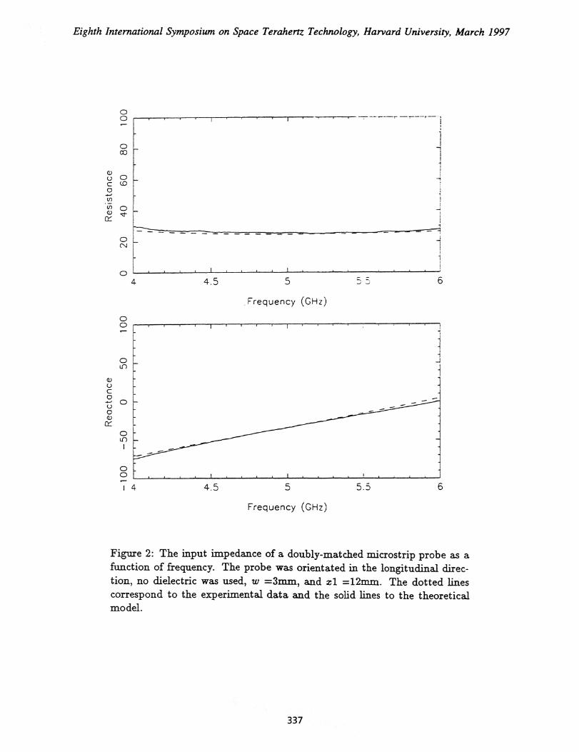
Figure 2: The input impedance of a doubly-matched microstrip probe as a.function of frequency. The probe was orientated in the longitudinal direc-tion, no dielectric was used, w =3mm., and xl =12ram. The dotted linescorrespond to the experimental data and the solid lines to the theoreticalmodel.
337

co
(1)0
C (0
(r) 0
0
Eighth International Symposium on Space Terahertz Technology, Harvard University, March 1997
4 4.5 5 5.5 6
Frequency (CHz)
I
4 4.5 5 5.5 6
Frequency (GHz)
Figure 3: The input impedance of a doubly-matched microstrip probe as afunction of frequency. The probe was orientated in the longitudinal direc-tion, the FIFE dielectric was 7mm thick, w .3ram., and xl .12mm. Thedotted lines correspond to the experimental data and the solid lines to thetheoretical model.
338

Eighth International Symposium on Space Terahertz Technology, Harvard University, March 1997
was 7mm thick and was made out of PTFE. Originally, we attemptedto use Nylon 66 because its dielectric constant is similar to that ofquartz. Unfortunately, however, although the reactive part of the in-put impedance agreed well with theory, the real part was higher thanpredicted and this seems to have been due to the known high lossesin Nylon 66. To remove the effects of reflections from the ends of thedielectric we tapered the substrate over a distance of approximately100mm In addition, we verified the effectiveness of the tapers by mea-suring the return loss, without a probe but with the dielectric, lookinginto into one end of the waveguide with the other terminated with amatch load. The reflections from the ends of the substrate were at alevel of below -15dB. A major advantage of the arrangement describedhere is that a short circuit can be applied at the wall of the waveguidein order to establish a well-defined reference plane for the impedancemeasurements. It is substantially more difficult to do well-calibratedimpedance measurements on an Eisenhart and Kahn probe.
In order to separate out the intrinsic behaviour of the probe fromthat of the the probe-backshort combination, we terminated both endsof the waveguide with matched loads. The real and imaginary parts ofthe input impedance were then measured by using a Vector NetworkAnalyser. In Fig. 2 we show the input impedance of a doubly-matchedprobe as a function of frequency. In this case the probe was 3mmwide and 12mm long and no dielectric was included. In Fig. 3 weshow the input impedance when a 7mm thick PTFE substrate wasincluded. Firstly, it can be seen that theory and experiment agreeextremely well in both cases. Secondly, it can be seen that the dielectricdoes influence the behaviour of the probe even in the case where thedielectric is relatively thin compared to the width of the waveguideand the dielectric constant is low. More specifically, the real part ofthe impedance is changed very little, but the imaginary part changessignificantly. The difference occurs of course because the imaginarypart is determined by local, non-propagating modes, whereas the realpart is determined by non-local propagating modes. An importantobservation is that the microstrip probe is essentially a low-impedancestructure with a typical input resistance in the range 10-60fi. Thisrange is ideally suited to the characteristic impedances of microstriplines. From the point of view of SIS mixers, the probe can be used for
339

_••••••
Eighth International Symposium on Space Terahertz Technology, Harvard University, March 1997
0 4 4.5 5 5.5 6
Frequency (GHz)
tr)
/
Lc)
1 4 4.5 5 5.5
Frequency (GHz)
Figure 4: The input impedance of a doubly-matched microstrip probe as a.function of frequency. The probe was orientated in the longitudinal direc-tion, the Nylon 66 dielectric was 7mm thick, w =3mm, and xl =9min. Thedotted lines correspond to the experimental data and the solid lines to thetheoretical model.
340

Eighth International Symposium on Space Terahertz Technology, Harvard University, March 1997
feeding SIS tunnel junctions over broad frequency ranges without theneed to reduce the height of the waveguide [11).
An important observation when performing the experiments wasthat for dielectric constants of 3.8, high-order modes can start to prop-agate in the dielectric-loaded waveguide, over the frequency range con-sidered, in addition to the lowest-order LSE and LSM modes. Thisleads to a stronger dependence on frequency than one would like. Theeffect is shown in Fig. 4 where Nylon 66 has been used in place of PTFE.The theoretical model cuts off at a frequency of 5.4 GI1z due to the on-set of high-order modes—although we could include them in the modelif desired—and the experimental data shows a peak due to a resonancebetween high-order modes. In the context of mixers this means that asthe substrate is made thicker the bandwidth of the probe is reduced.This behaviour and the frequency at which it occurs is fully predictedand can be understood by means of our theory. In fact we find, forpractical mixers, that high-order modes in the probe are more influ-ential in determining the bandwidth than high-order modes in the IFchannel [12]. Another notable feature of Fig. 4 is that experiment andtheory do not agree when one looks at the real part of the impedance,but they do agree when one looks at the reactive part. We believe thatthis effect is due to the very high microwave losses that are known tobe associated with Nylon 66.
Iv Conclusions
We have derived an expression for the input impedance of a microstripprobe in waveguide. In the case where the dielectric is extremely thinand can be neglected, the expression can be reduced to a very simpleanalytical form. In the case where the dielectric is taken into account,the expression is more complicated but straightforward to evaluate nu-merically. A major advantage of developing a theory of this kind, oversimply relying on three-dimensional electromagnetic simulators, is thatone gets a clear understanding of the underlying physics involved.
Our work on microstrip waveguide probes leads us to the followingconclusions:
1. For the two-sided probe the effects of the propagating and non-propagating modes add up in parallel leading to a high input
341
Eighth International Symposium on Space Terahertz Technology, Harvard University, March 1997
impedance with a narrow bandwidth. This is intrinsic to thestructure and can only be overcome by reducing the height ofthe waveguide. For the one-sided probe the impedances associ-ated with the individual modes add up in series leading to a low-impedance broadband structure. In fact only the lowest-orderpropagating mode makes a contribution to the real part of theinput impedance.
2. With the one-sided probe a low-impedance broad-band structurecan be made without reducing the height of the waveguide. Infact for THz operation it may well be possible to use oversizewaveguide.
3. For the one-sided probe we have shown that the axial orientationof the film has very little influence on the input impedance, mean-ing that the orientation can be chosen for mechanical conveniencealone. To our knowledge this is the first time that this effect hasbeen proven theoretically.
4. When a supporting dielectric substrate is included, the modal be-haviour becomes more complicated and it is necessary to keep thesubstrate thiner than some certain value to avoid resonances andachieve broad-band operation. Normally, one keeps the substratethin to avoid high-order modes in the IF filter and not to avoidhigh-order modes in the probe. In practice it seems that the probedictates how thick the substrate should be.
In summary, we feel that a well-designed one-sided probe is betterthan a two-sided probe.
References
[11 R.L. Eisenhart and P.J. Khan, "Theoretical and experimentalanalysis of a waveguide mounting structure," IEEE Trans. Mi-crowave Theory Tech., vol. MTT-19, pp. 706-717, 1971.
[2] G. Yassin and S. Withington, "Analytical expression for the inputimpedance of a microstrip probe in waveguide," Int. J. InfraredMillimeter Waves, vol. 17, pp. 1685-1705, 1996.
342
Eighth International Symposium on Space Terahertz Technology, Harvard University, March 1997
[3] R.E. Collin, Field Theory of Guided Waves, IEEE Press: NewYork, pp. 471-483, 1991.
[4] F. Chen and W. B. Dou ,"Full-wave analysis of a waveguide-to-microstrip transition for millimeter wave applications," Int. J.Infrared and Millimeter Waves, vol. 16, pp. 641-652, 1995.
[5] T.Q. Ho and Yi-Chi Shih, "Spectral-domain analysis of E-planewaveguide to inicrostrip transition," IEEE Trans. MicrowaveTheory Tech., vol. MTT-37, pp. 388-392, 1989.
[6] W.L. Weeks, it Electromagnetic Theory for Engineering Appli-cations, John Wiley Sc Sons, Inc.: New York, 1964.
[7] V.II. Rumsey "Reaction concept in electromagnetic theory,"Phys. Rev., vol. 94, pp. 1483-1491, 1954.
[8] R.E. Collin, Field Theory of Guided Waves, McGraw-Hill: NewYork, 1960.
[9] S. Withington, G. Yassin, M. Buffey, and C. Norden, "A horn-reflector antenna for high-performance submillimetre-wave imag-ing arrays," Int. J. Infrared and Millimeter Waves, vol. 18, pp.341-358, 1997.
[10] T. Uwano and T. Itoh, "Spectral Domain Approach," in Nu-merical Techniques for Microwave and Millimeter-Wave PassiveStructures, Ed. T. Itoh, John Wiley 86 Sons, New York, 1989.
[11] A.R. Kerr and S.-K. Pan, "Some recent developments in the de-sign of SIS mixers," Int. J. Infrared Millimeter Waves, vol. 11,pp. 1169-1187, 1990.
{12] S. Withington and G. Yassin, "Spectral-Domain Analysis ofSubreillimetre-Wave Microstrip Filters," Int. J. Infrared and Mil-limeter Waves, vol. 14, pp. 1975-1984, 1993.
343