Embed Size (px)
Citation preview
PH-315 A. La Rosa
INPUT and OUTPUT IMPEDANCE I. PURPOSE To familiarize with the concept of input and output impedance of a circuit. Evaluate the benefits of using of transistors to design “stiffer” electronic circuits.
II. THEORETICAL CONSIDERATIONS
II.A The concept of circuit loading
II.B The emitter-follower circuit II.B.1 Calculation of the effective (load) input impedance Zin in the emitter-
follower circuit II.B.2 Calculation of the effective (source) output impedance Zout in the emitter-
follower circuit II.B.3 Alternative derivation of the output and input impedances.
III. EXPERIMENTAL CONSIDERATIONS
III.1 Making stiffer sources: Emitter follower
III.1A Biasing the emitter follower III.1B Input impedance of the emitter-follower circuit III.1C Output impedance of the emitter-follower circuit
III.2 Matching impedance: measuring the 50 output impedance. Appendix-1 Thevenin equivalent circuit analysis
Appendix-2
II.A The concept of circuit loading
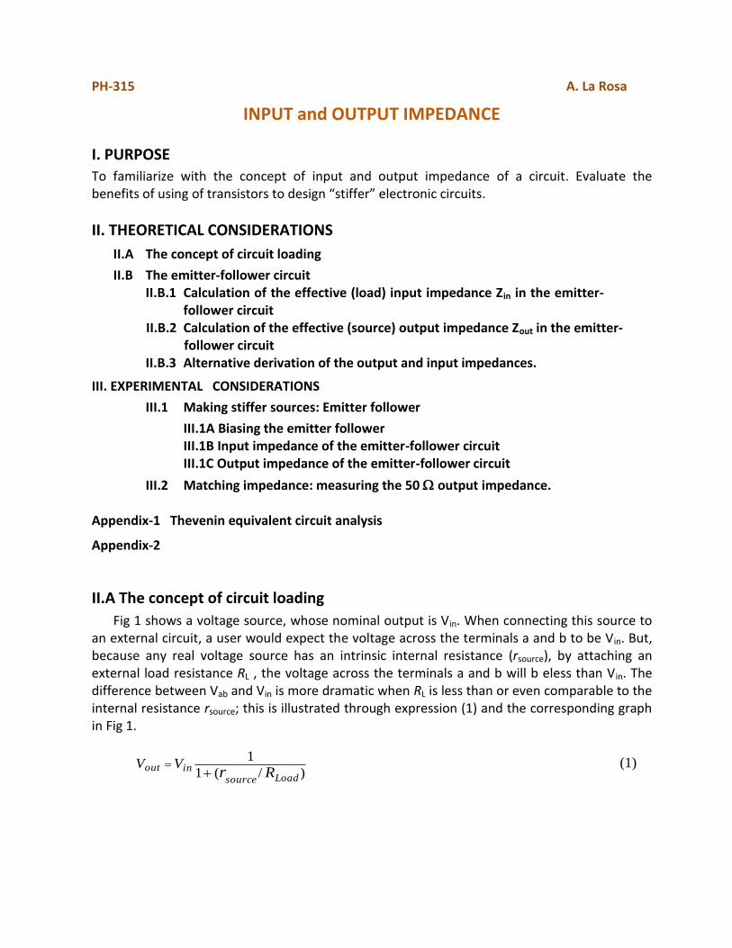
Fig 1 shows a voltage source, whose nominal output is Vin. When connecting this source to an external circuit, a user would expect the voltage across the terminals a and b to be Vin. But, because any real voltage source has an intrinsic internal resistance (rsource), by attaching an external load resistance RL , the voltage across the terminals a and b will b eless than Vin. The difference between Vab and Vin is more dramatic when RL is less than or even comparable to the internal resistance rsource; this is illustrated through expression (1) and the corresponding graph in Fig 1.
)/(1
1
Loadsourceinout Rr
VV
(1)
rsource
Vin
b b
RLoad
Vin
Vout
Vout
rsource
rsource
RLoad
Open circuit
Vab =Vin Vab <Vin
Vin/2
a a
Vin
Fig. 1 “Circuit loading” refers to the undesirable reduction of the open-circuit voltage Vab by the load.
Solution to avoid “loading” the circuit: Use RLoad >> r source
(Rule of thumb: To use RLoad > 10 r source )
Connecting circuits one after another In electronic circuits, stages are connected one after another.
i) Sometimes it is OK to load the circuit, as far as we know how much the loaded is, and particularly if Zin is going to be constant.
ii) Of course, it is always better to have a “stiff source” (Zout << Zin), so that signal levels do not change when a load is connected.
iii) However, there are situations in which it is rather required to have Zout = Zin. That is the case in radiofrequency circuits to avoid signal reflections.
So, be aware to respond accordingly depending on the situation.
Zout-1
Zin-2
Amplifier-1 Amplifier-2
Fig. 2 Amplifiers are typically characterized by their effective output and input impedances. This is particularly important for analysis when cascading them one after another.
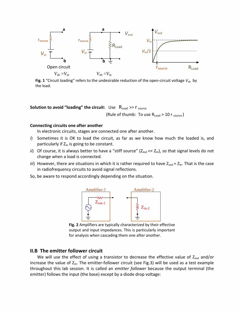
II.B The emitter follower circuit We will use the effect of using a transistor to decrease the effective value of Zout and/or
increase the value of Zin. The emitter-follower circuit (see Fig.3) will be used as a test example throughout this lab session. It is called an emitter follower because the output terminal (the emitter) follows the input (the base) except by a diode drop voltage:
V0.6VV BE (2)
The output voltage Vout (in this case coinciding with VE) is a replica of the input voltage, except for the diode voltage 0.6 V to 0.7 V.
Vin must stay at 0.6 V or more, otherwise the transistor will be off and the output will stay at ground. By connecting the emitter resistor RE to a negative voltage supply, one can allow negative input voltages as well. Keep this in mind for your experimental section.
RE
B C
E
Vin
Vout
10V
Vin
0V
R2
50K
R1
5.6 K
Fig. 3 Emitter follower circuit.
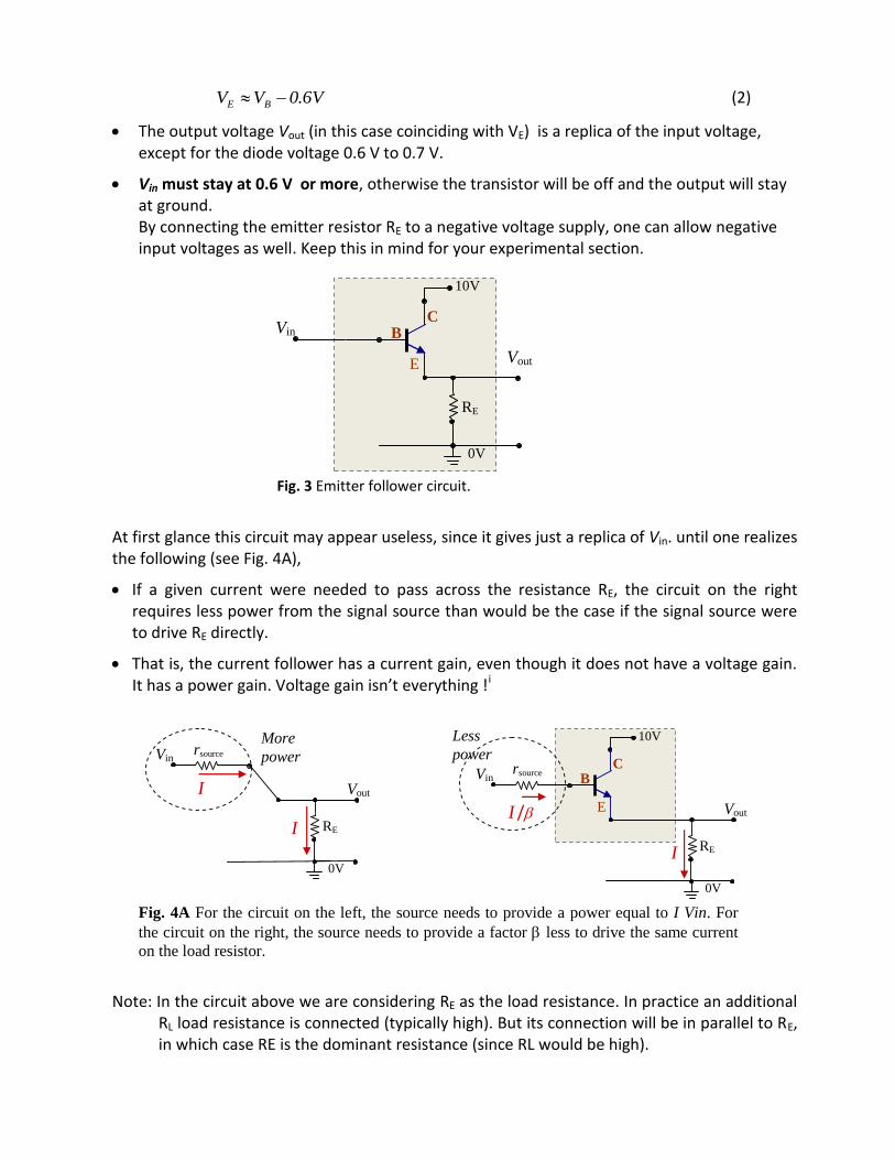
At first glance this circuit may appear useless, since it gives just a replica of Vin. until one realizes the following (see Fig. 4A),
If a given current were needed to pass across the resistance RE, the circuit on the right requires less power from the signal source than would be the case if the signal source were to drive RE directly.
That is, the current follower has a current gain, even though it does not have a voltage gain. It has a power gain. Voltage gain isn’t everything !i
RE
B C
E
Vin
Vout
10V
0V
RE
Vin
Vout
0V
rsource
rsource
I I /
I
I
More
power
Less
power
Fig. 4A For the circuit on the left, the source needs to provide a power equal to I Vin. For
the circuit on the right, the source needs to provide a factor less to drive the same current
on the load resistor.
Note: In the circuit above we are considering RE as the load resistance. In practice an additional
RL load resistance is connected (typically high). But its connection will be in parallel to RE, in which case RE is the dominant resistance (since RL would be high).
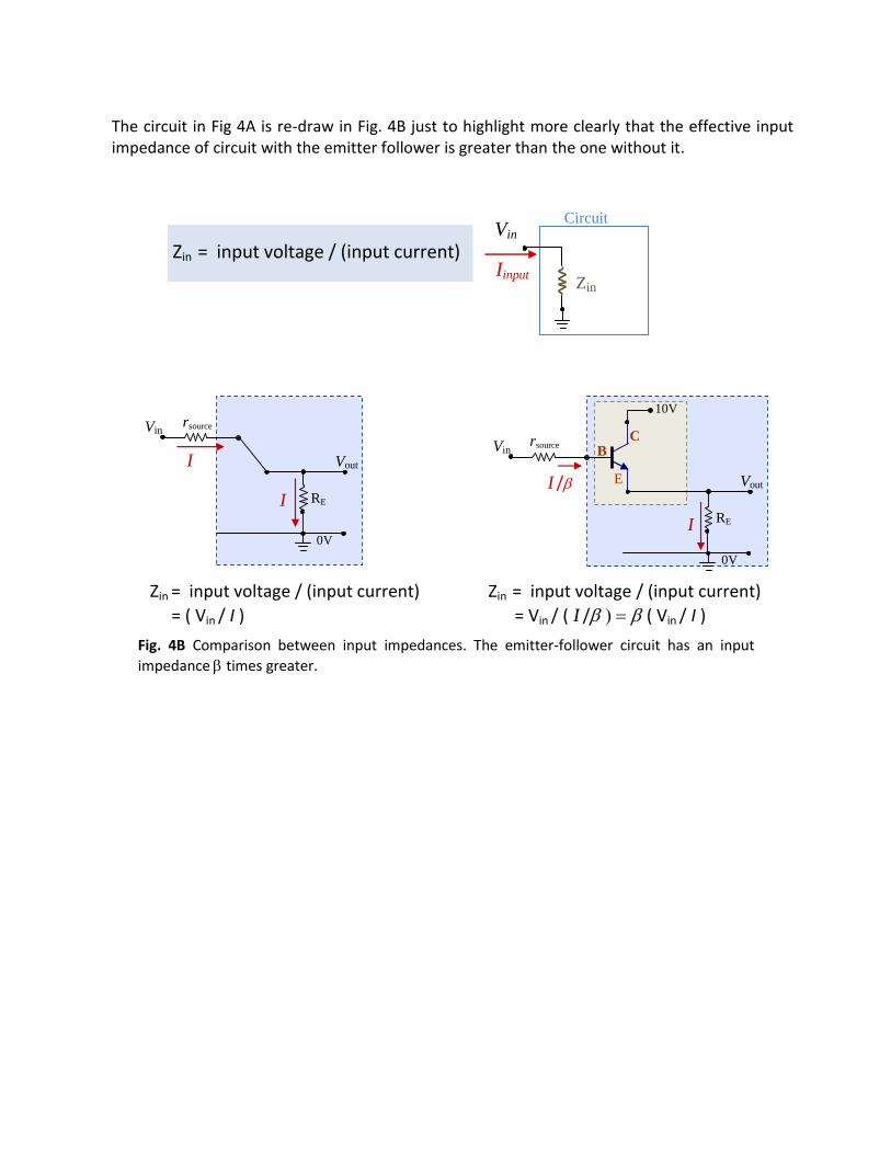
The circuit in Fig 4A is re-draw in Fig. 4B just to highlight more clearly that the effective input impedance of circuit with the emitter follower is greater than the one without it.
Zin
Zin = input voltage / (input current)
Circuit
Iinput
Vin
RE
B C
E
Vin
Vout
10V
0V
RE
Vin
Vout
0V
rsource
rsource
I I /
I
I
Zin = input voltage / (input current) Zin = input voltage / (input current)
= ( Vin / I ) = Vin / ( I /( Vin / I )
Fig. 4B Comparison between input impedances. The emitter-follower circuit has an input
impedance times greater.
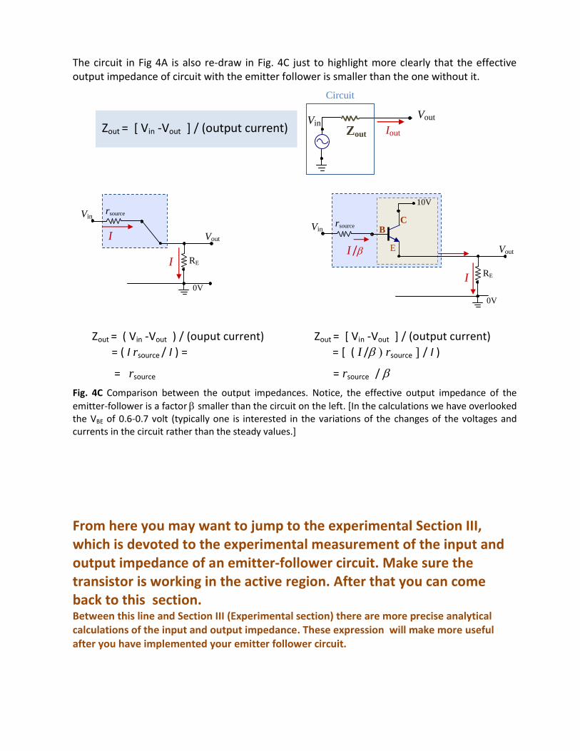
The circuit in Fig 4A is also re-draw in Fig. 4C just to highlight more clearly that the effective output impedance of circuit with the emitter follower is smaller than the one without it.
Zout
Iout
Vout
Vin
Zout = [ Vin -Vout ] / (output current)
Circuit
RE
B C
E
Vin
Vout
10V
0V
RE
Vin
Vout
0V
rsource
rsource
I I /
I
I
Zout = ( Vin -Vout ) / (ouput current) Zout = [ Vin -Vout ] / (output current)
= ( I rsource / I ) = = [ ( I / rsource/ I )
= rsource = rsource/
Fig. 4C Comparison between the output impedances. Notice, the effective output impedance of the
emitter-follower is a factor smaller than the circuit on the left. [In the calculations we have overlooked the VBE of 0.6-0.7 volt (typically one is interested in the variations of the changes of the voltages and currents in the circuit rather than the steady values.]
From here you may want to jump to the experimental Section III, which is devoted to the experimental measurement of the input and output impedance of an emitter-follower circuit. Make sure the transistor is working in the active region. After that you can come back to this section. Between this line and Section III (Experimental section) there are more precise analytical calculations of the input and output impedance. These expression will make more useful after you have implemented your emitter follower circuit.
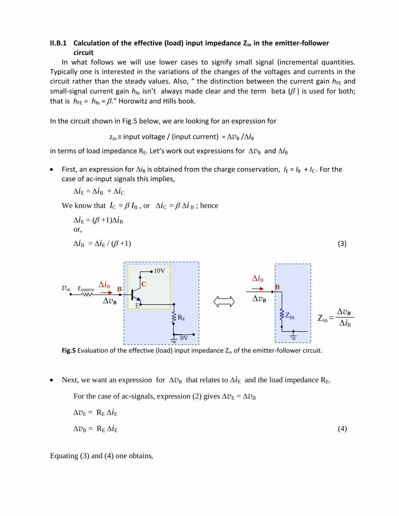
II.B.1 Calculation of the effective (load) input impedance Zin in the emitter-follower circuit
In what follows we will use lower cases to signify small signal (incremental quantities. Typically one is interested in the variations of the changes of the voltages and currents in the circuit rather than the steady values. Also, “ the distinction between the current gain hFE and
small-signal current gain hfe isn’t always made clear and the term beta () is used for both;
that is hFE = hfe = .” Horowitz and Hills book.
In the circuit shown in Fig.5 below, we are looking for an expression for
zin ≡ input voltage / (input current) = vB /iB
in terms of load impedance RE. Let’s work out expressions for vB and iB
First, an expression for iB is obtained from the charge conservation, IE = IB + IC . For the case of ac-input signals this implies,
iE = iB + iC
We know that IC = IB , or iC = i B ; hence
iE = ( +1)iB
or,
iB = iE / ( +1) (3)
vB
iB
Zin =
RE
B C
E
vin
10V
0V
rsource
Equivalent
Zin
iB
vB
B iB
vB
Fig.5 Evaluation of the effective (load) input impedance Zin of the emitter-follower circuit.
Next, we want an expression for vB that relates to iE and the load impedance RE.
For the case of ac-signals, expression (2) gives vE = vB
vE = REiE
vB = REiE (4)
Equating (3) and (4) one obtains
Ein Ri
ZB
)1(
Bv
(5)
Since is typically of the order of 100, then Zin is ~ 100 times greater than RE. For RE = 0.5 k,
Zin ~ 50 k
[Notice the mathematical derivation above is independent of the particular accessory to the
circuit (see Fig. 5) that may be used to experimentally measure iB and vB. It only requires that
the transistor is properly biased (i.e. working in the active region, so one can justify the use of
the expression IC = IB.]
R2
50K
R1
5.6 K
vin
RE
B C
E
vin
10V
0V
Equivalent
Zin = (+1)RE
iB
vB
B rsource rsource
Fig.6 HIGHER (LOAD) INPUT IMPEDANCE. The presence of the transistor has the net effect to
increasing the (load) impedance RE by a factor of . “The emitter-follower has high input
impedance”.
II.B.2 Calculation of the effective (source) output impedance Zout in the emitter-follower circuit
We will use upper case for DC voltages (like VBB and IB) and the lower case used for AC
small-signals (like vin, iB, and vout). In the circuit shown in Fig.7 below, we are looking for an expression for
Zout ≡ [ vin -vout ] / (output current)
= (vin -vB) /iE
in terms of source impedance rsource.
RE
B C
E
vin
Vout
10V
Vin
0V
R2
50K
R1
5.6 K
rsource
RE
vin
vout
0V
Zout
Equivalent
iE iE
vE
ut
iE
Zout =
vin - vE
Fig.7 Evaluation of the effective (source) output impedance Zout of the emitter-follower circuit.
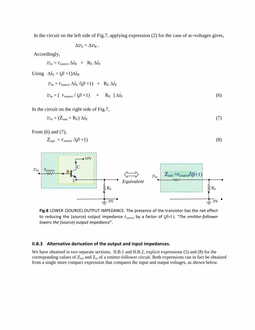
In the circuit on the left side of Fig.7, applying expression (2) for the case of ac-voltages gives,
vE = vB .
Accordingly,
vin = rsource iB + RE iE
Using iE = ( +1)iB
vin = rsource iE /( +1) + RE iE
vin = [ rsource / ( +1) + RE ] iE (6)
In the circuit on the right side of Fig.7,
vin = (Zout + RE) iE (7)
From (6) and (7),
Zout = rsource /( +1) (8)
RE
B C
E
vin
Vout
10V
Vin
0V
R2
50K
R1
5.6 K
rsource
RE
vin
vout 0V
Zout =rsource/(+1)
Equivalent
Fig.8 LOWER (SOURCE) OUTPUT IMPEDANCE. The presence of the transistor has the net effect
to reducing the (source) output impedance rsource by a factor of (. “The emitter-follower lowers the (source) output impedance”.
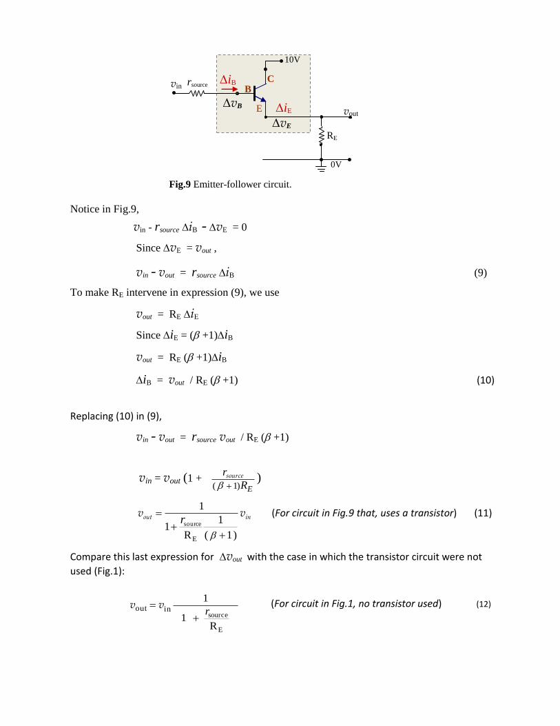
II.B.3 Alternative derivation of the output and input impedances.
We have obtained in two separate sections, II.B.1 and II.B.2, explicit expressions (5) and (8) for the
corresponding values of Zout and Zin of a emitter-follower circuit. Both expressions can in fact be obtained
from a single more compact expression that compares the input and output voltages, as shown below.
RE
B C
E
vin
vout
10V
Vin
0V
R2
50K
R1
5.6 K
RE
Vin
Vout
0V
rsource
rsource
iB
vB iE
vE
Fig.9 Emitter-follower circuit.
Notice in Fig.9,
vin - rsourceiB - vE = 0
Since vE = vout ,
vin - vout = rsourceiB (9)
To make RE intervene in expression (9), we use
vout = REiE
Since iE = ( +1)iB
vout = RE( +1)iB
iB = vout / RE( +1) (10)
Replacing (10) in (9),
vin - vout = rsource vout / RE( +1)
vin = vout (1 + ER
r
)1 ( source )
inout vv
) 1 (
1
R1
1
E
source
r (For circuit in Fig.9 that, uses a transistor) (11)
Compare this last expression for vout with the case in which the transistor circuit were not
used (Fig.1):
R
1
1
E
sourceinout r
vv (For circuit in Fig.1, no transistor used) (12)
Notice in (11), one obtains the same result whether
- Considering an effective (source) output impedance rsource / (+1) and load impedance RE, or
- Considering a (source) output impedance rsource and an effective input impedance
RE(+1).
III. EXPERIMENTAL CONSIDERATIONS
III.1 Making stiffer sources: Emitter follower
III.1A Biasing the emitter follower III.1B Input impedance of the emitter-follower circuit III.1C Output impedance of the emitter-follower circuit
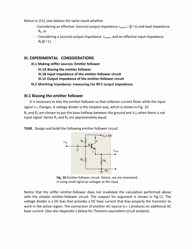
III.1 Biasing the emitter follower
It is necessary to bias the emitter-follower so that collector current flows while the input
signal vin changes. A voltage divider is the simplest way, which is shown in Fig. 10.
R1 and R2 are chosen to put the base halfway between the ground and VCC when there is not input signal. Hence R1 and R2 are approximately equal.
TASK. Design and build the following emitter-follower circuit
RE
B C
E
vin
in
vout
VCC=10V
R1
R2
Vin
0V
R2
50K
R1
5.6 K
C
Fig. 10 Emitter follower circuit. Notice, we are interested in using small signal ac-voltages at the input
Notice that the stiffer emitter-follower does not invalidate the calculation performed above with the simpler emitter-follower circuit. The support for argument is shown in Fig.11. The voltage divider is a DC bias that provides a DC base current that bias properly the transistor to
work in the active region. The connection of another AC-source (vin ) produces an additional AC base current. (See also Appendix-1 below for Thevenin equivalent circuit analysis).
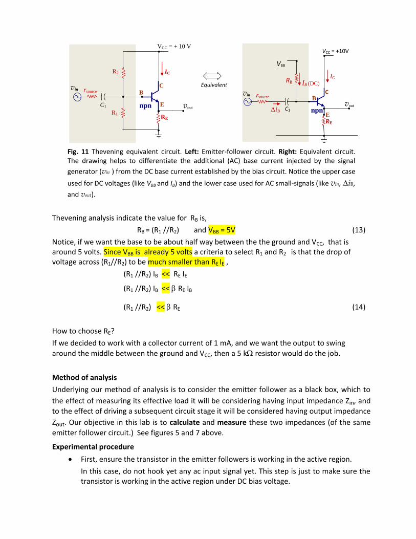
npn E
VCC = + 10 V
RE
R2
B
vout
C
IC
R1
vin rsource
Try rsource = 1 K
C1
C2
Equivalent
Try rsource = 1 K
Equivalent
npn E RE
RB
B C
VBB
VCC = +10V
IB (DC)
IC
iB
vin
vout
rsource
C2
C1
Fig. 11 Thevening equivalent circuit. Left: Emitter-follower circuit. Right: Equivalent circuit. The drawing helps to differentiate the additional (AC) base current injected by the signal
generator (vin ) from the DC base current established by the bias circuit. Notice the upper case
used for DC voltages (like VBB and IB) and the lower case used for AC small-signals (like vin, iB,
and vout).
Thevening analysis indicate the value for RB is,
RB = (R1 //R2) and VBB = 5V (13)
Notice, if we want the base to be about half way between the the ground and VCC, that is around 5 volts. Since VBB is already 5 volts a criteria to select R1 and R2 is that the drop of voltage across (R1//R2) to be much smaller than RE IE ,
(R1 //R2) IB << RE IE
(R1 //R2) IB << RE IB
(R1 //R2) << RE (14)
How to choose RE?
If we decided to work with a collector current of 1 mA, and we want the output to swing
around the middle between the ground and VCC, then a 5 k resistor would do the job.
Method of analysis
Underlying our method of analysis is to consider the emitter follower as a black box, which to
the effect of measuring its effective load it will be considering having input impedance Zin, and
to the effect of driving a subsequent circuit stage it will be considered having output impedance
Zout. Our objective in this lab is to calculate and measure these two impedances (of the same
emitter follower circuit.) See figures 5 and 7 above.
Experimental procedure
First, ensure the transistor in the emitter followers is working in the active region.
In this case, do not hook yet any ac input signal yet. This step is just to make sure the transistor is working in the active region under DC bias voltage.
Measure VEB
Measure the base current, and verify if the value agrees with the Thevenin analysis.
Next, apply an ac input voltage vin.
Use a coupling capacitor (try C1= 0.1 F, for example).
For a given input frequency (1 kHz, for example), increase gradually the amplitude and check the max amplitude the circuit tolerates before the output signal gets distorted.
Establish the range of frequency at which the circuit works as an emitter follower.
Find out what happens when the frequency is lowered. Check if there is distortion when too low frequencies are used.
Repeat the procedure above by experimenting a smaller capacitance (10 nF).
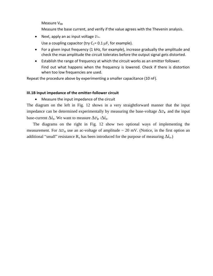
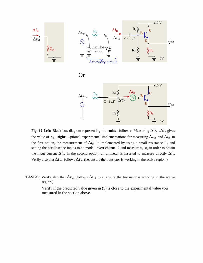
III.1B Input impedance of the emitter-follower circuit
Measure the input impedance of the circuit
The diagram on the left in Fig. 12 shows in a very straightforward manner that the input
impedance can be determined experimentally by measuring the base-voltage vB and the input
base-current iB. We want to measure vB /iB.
The diagrams on the right in Fig. 12 show two optional ways of implementing the
measurement. For vin use an ac-voltage of amplitude ~ 20 mV. (Notice, in the first option an
additional “small” resistance Rx has been introduced for the purpose of measuring iB.)
RE
B C
E
Rx
2 Oscillos-
cope
iB
Zin
iB
vB
0V
Transformer
vB
1
vin
Accessory circuit
vout
R2
R1
RE
B C
E
Rx
iB
0V
vB vin
vout
R2
R1
10 V
10 V
A
Or
C= 1 F
C= 1 F
Fig. 12 Left: Black box diagram representing the emitter-follower. Measuring vB /iB gives
the value of Zin. Right: Optional experimental implementations for measuring vB and iB. In
the first option, the measurement of iB is implemented by using a small resistance Rx and
setting the oscilloscope inputs to ac-mode; invert channel 2 and measure v1–v2 in order to obtain
the input current iB. In the second option, an ammeter is inserted to measure directly iB.
Verify also that vout follows vB (i.e. ensure the transistor is working in the active region.)
TASKS: Verify also that vout follows vB (i.e. ensure the transistor is working in the active
region.)
Verify if the predicted value given in (5) is close to the experimental value you
measured in the section above.
Vin
RE
rsourc
e
Source
vin vout
rsource
Source
vin
Input impedance: RE
Effective input impedance:
(1 + ) RE
RE
B C
E
10 V
0V
Vout
R2
R1
C= 1 F
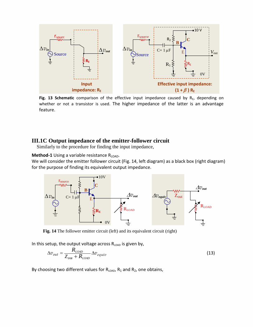
Fig. 13 Schematic comparison of the effective input impedance caused by RE, depending on
whether or not a transistor is used. The higher impedance of the latter is an advantage feature.
III.1C Output impedance of the emitter-follower circuit Similarly to the procedure for finding the input impedance,
Method-1 Using a variable resistance RLOAD. We will consider the emitter follower circuit (Fig. 14, left diagram) as a black box (right diagram) for the purpose of finding its equivalent output impedance.
Zout
vequiv
RLOAD RE
B C
E
10V
0V
rsource
vin
RLOAD
vout
vout C= 1 F
Fig. 14 The follower emitter circuit (left) and its equivalent circuit (right)
In this setup, the output voltage across RLOAD is given by,
equivout vv LOADt
LOAD
RR
ouZ (13)
By choosing two different values for RLOAD, R1 and R2, one obtains,
out
Zout
vequiv
R1
vout
out
Zout
vequiv
R2
vout
Fig. 15 The equivalent follower emitter circuit hooked to two different output loads.
equivout;1 vv 1
1
RR
touZ and equivout;2 vv
2
2
RR
touZ
Solving for Zout (see proof at the end of these notes, appendix 2),
1
1
1
2
2
out;2
out;1
out;2
out;1
v
v
v
v
R
R
RZ tou (14)
As we expect Zout to be very low ( ≤ 100 ) compared to the input impedance, you may have to use very low values for R1 and R2 (potentially 30 Ohms).
Alternatively, in the description above, R1 can be the input impedance of the oscilloscope, and R2 a low value resistance R2. i) Connect the output to the oscilloscope (assumed here that the impedance of the
oscilloscope is infinite; RLOAD = R1 = ). This allows measuring the amplitude of vequiv .
equivout,1 vv LOADt
LOAD
R
R
ouZ equivv
1
1
R
R
touZ equivv
1R
That is,
out,1v equivv (measured by simply connecting the output
of the transistor to the oscilloscope.)
ii) Use an arbitrary external resistance R2 (typically low values work better, like 30 Ohms for
example) as RLOAD , and measure the corresponding out.2v .
equivout,2 vv 2
2
R
R
touZ
out,2
equiv
v
v
2
2)(R
Z Rtou
11 22
out,2
out,1
out,2
equiv
v
v
v
vRRZ tou
Note about checking the results: Even if you get smaller values for Zout, how to know if the results make sense? That is, how do we know the output resistance without and with the transistor has decrease by a factor
of ? In fact, the latter may not have been fulfilled (check your results once you measure independently the output impedance of your signal generator, as requested in the next section of this lab).
One alternative way to verify our results is to do the following:
Insert a resistance of 1k ohm between the ac-voltage source and your circuit. That is, we are adding a 1k ohm to the output impedance. Repeat the procedure to measure Zout.
Check if your new results has increased the value for Zout by 1k/.
Method-2 The shortcoming of method-1 is that it requires the testing RLOAD (Fig. 14) to be too small (which may disturb the working point of the transistor). Another way is to use the circuit of Fig. 13 and measure directly,
Zout ≡ [ vin - vout ] / (output current)
= (vin - vout) /iE
This will require to measure vin -vout , which will be very small. One way to attempt its
measurement is to use the oscilloscope to monitor vin (in channel-1) and vout (in channel-2),
invert the second signal, and then use the scope in summing mode. For iE you can use
(vout) / RE
In both methods, be aware of the role played by the capacitor impedance. Choose the proper frequency such that a) the capacitor impedance is minimum, but at the same time b) the used frequency is within the frequency-bandwidth response of the transistor.
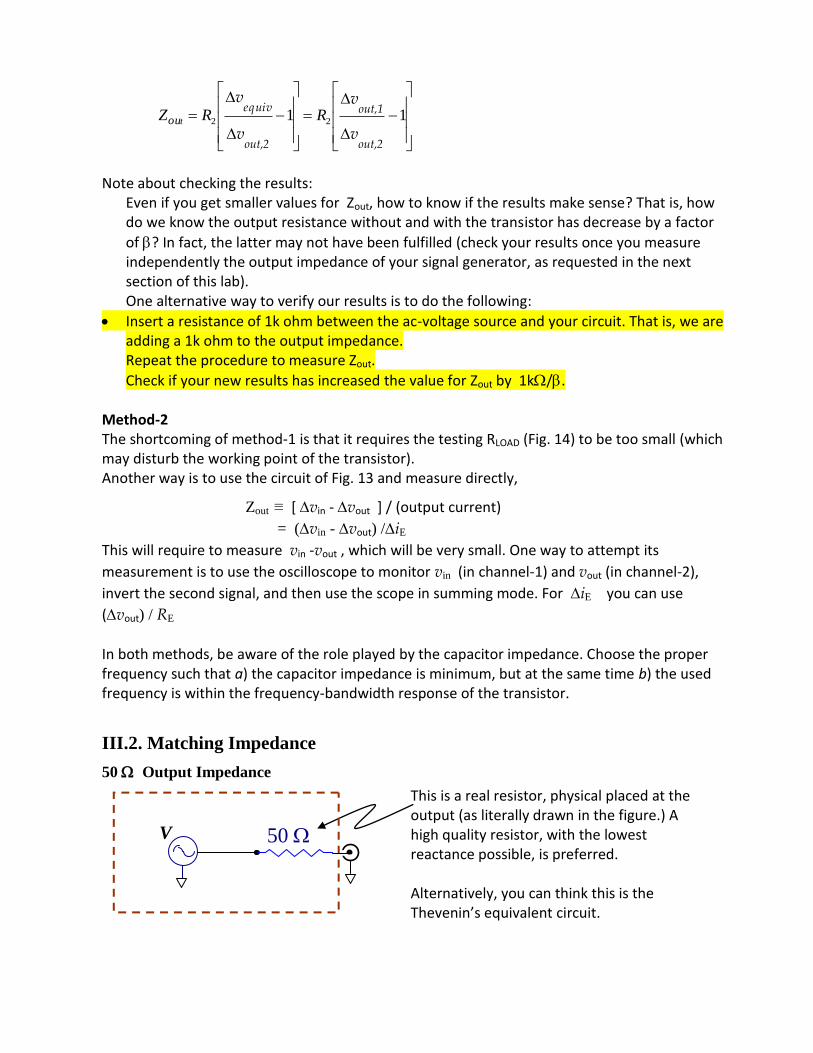
III.2. Matching Impedance
50 Output Impedance
50
This is a real resistor, physical placed at the output (as literally drawn in the figure.) A high quality resistor, with the lowest reactance possible, is preferred. Alternatively, you can think this is the Thevenin’s equivalent circuit.
V
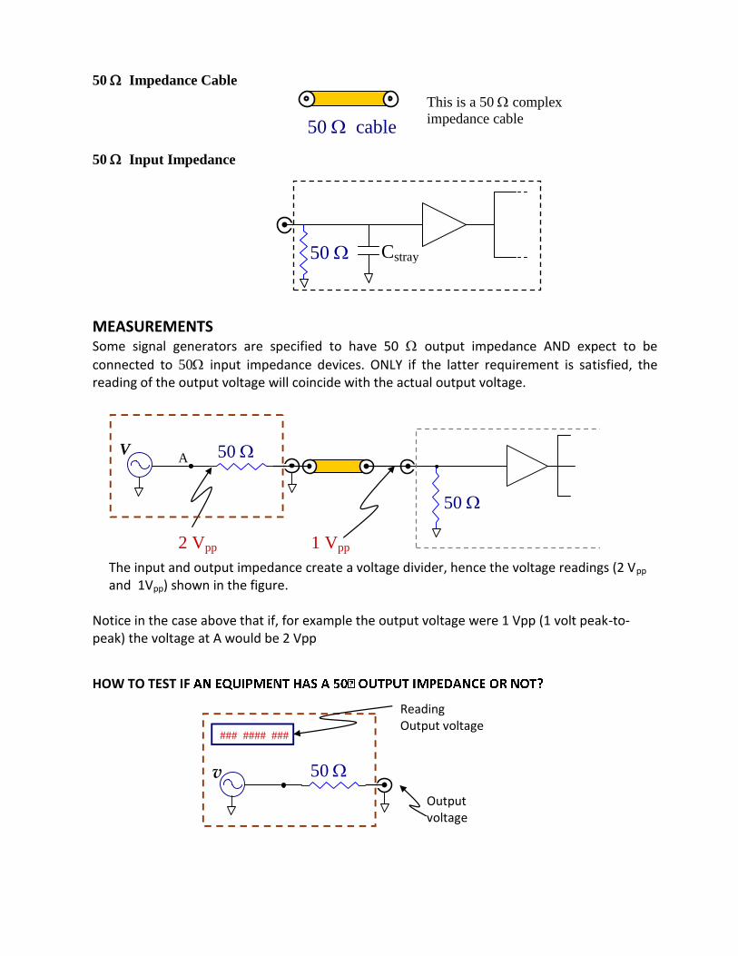
50 Impedance Cable
50 cable
This is a 50 complex
impedance cable
50 Input Impedance
50 Cstray
MEASUREMENTS Some signal generators are specified to have 50 output impedance AND expect to be
connected to 50 input impedance devices. ONLY if the latter requirement is satisfied, the reading of the output voltage will coincide with the actual output voltage.
2 Vpp
50
50
1 Vpp
V A
The input and output impedance create a voltage divider, hence the voltage readings (2 Vpp and 1Vpp) shown in the figure.
Notice in the case above that if, for example the output voltage were 1 Vpp (1 volt peak-to-peak) the voltage at A would be 2 Vpp
HOW TO TEST IF
Output voltage
50 v
Reading Output voltage
### #### ###
Task: Verify whether or not your signal generator has a 50 output impedance.
i)
ii)
50 V A To oscilloscope Expected output
voltage: VA Output
Now, connect a 50 resistor as shown in the figure below. If the voltage drops to 50%, then
the output impedance is 50.
50
50
v
A To oscilloscope Expected output
voltage: (1/2) vA Output
Appendix-: Thevenin equivalent circuit analysis
The example presented here is for a transistor amplifier circuit. But the essence of the Thevening
analysis is valid also for a emitter-follower circuit.
We can use the Thevenin’s theorem to show the equivalence between the circuits in Fig. 9 and
Fig. 11.
IC
VCE
100 A
20 mA
CR
15V
+ 15 V
P
VCE
IC IB=50 A IB
B
E
RC
RB
B VCE
C
IC
IB Vin
VCC (+ 15 V)
Vout
Fig. 9
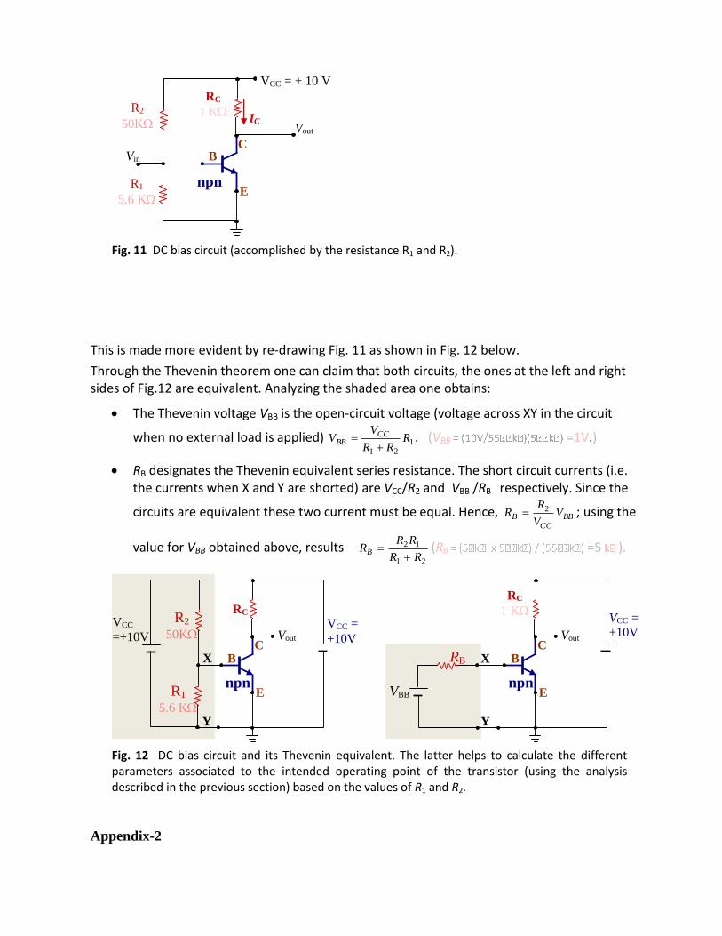
R1
5.6 K
npn E
VCC = + 10 V
RC
1 K
R2
50K
B
Vout
C
IC
Vin
Fig. 11 DC bias circuit (accomplished by the resistance R1 and R2).
This is made more evident by re-drawing Fig. 11 as shown in Fig. 12 below.
Through the Thevenin theorem one can claim that both circuits, the ones at the left and right sides of Fig.12 are equivalent. Analyzing the shaded area one obtains:
The Thevenin voltage VBB is the open-circuit voltage (voltage across XY in the circuit
when no external load is applied) 121
RRR
VV CC
BB
. (VBB =1V.)
RB designates the Thevenin equivalent series resistance. The short circuit currents (i.e. the currents when X and Y are shorted) are VCC/R2 and VBB /RB respectively. Since the
circuits are equivalent these two current must be equal. Hence, BBCC
B VV
RR 2 ; using the
value for VBB obtained above, results 21
12
RR
RRRB
(RB =5 ).
npn E
X
RC R2
50K
B
Vout C
R1
5.6 K
VCC =
+10V
npn E
RB B
Vout C
VBB
VCC =
+10V
Y
X
Y
VCC
=+10V
RC
1 K
Fig. 12 DC bias circuit and its Thevenin equivalent. The latter helps to calculate the different parameters associated to the intended operating point of the transistor (using the analysis described in the previous section) based on the values of R1 and R2.
Appendix-2
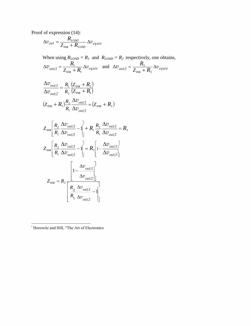
Proof of expression (14):
equivout vv LOADt
LOAD
RR
ouZ
When using RLOAD = R1 and RLOAD = R2 respectively, one obtains,
equivout;1 vv 1
1
RR
touZ and equivout;2 vv
2
2
RR
touZ
1
2
2
1
RR
t
t
ou
ou
Z
Z
R
R
out;2
out;1
v
v
2
1
21 RR tt ouou Z
R
RZ
out;2
out;1
v
v
2
1
21
1
2 1 RRR
R
R
RZ tou
out;2
out;1
out;2
out;1
v
v
v
v
out;2
out;1
out;2
out;1
v
v
v
v12
1
2 1 RR
RZ tou
1
1
1
2
2
out;2
out;1
out;2
out;1
v
v
v
v
R
R
RZ tou
i Horowitz and Hill, “The Art of Electronics