Embed Size (px)
Citation preview
AM3517, AM3505 Sitara™ ProcessorsSilicon Revisions 1.1, 1.0
Silicon Errata
Literature Number: SPRZ306EOctober 2009–Revised September 2016
2 SPRZ306E–October 2009–Revised September 2016Submit Documentation Feedback
Copyright © 2009–2016, Texas Instruments Incorporated
Table of Contents
Contents
1 Introduction......................................................................................................................... 41.1 Device and Development Support Tool Nomenclature ............................................................. 41.2 Revision Identification ................................................................................................... 5
2 Silicon Revision 1.1 Usage Notes and Known Design Exceptions to Functional Specifications..... 62.1 Usage Notes for Silicon Revision 1.1.................................................................................. 62.2 Silicon Revision 1.1 Known Design Exceptions to Functional Specifications .................................. 11
3 Silicon Revision 1.0 Usage Notes and Known Design Exceptions to Functional Specifications ... 653.1 Usage Notes for Silicon Revision 1.0 ................................................................................ 653.2 Silicon Revision 1.0 Known Design Exceptions to Functional Specifications .................................. 65
Revision History.......................................................................................................................... 68
www.ti.com
3SPRZ306E–October 2009–Revised September 2016Submit Documentation Feedback
Copyright © 2009–2016, Texas Instruments Incorporated
List of Figures
List of Figures1 Example, Device Revision Codes for AM35x Microprocessor (ZCN Package) ..................................... 52 AM35x USB Modules........................................................................................................ 83 High-Speed USB Host Subsystem Highlight ............................................................................. 94 Connecting to High-Speed PHYs Using USB Ports ................................................................... 105 Connecting to a High-Speed USB Hub.................................................................................. 106 I2C Flowchart ............................................................................................................... 187 SPI Dummy DMA RX Generation........................................................................................ 208 Dummy DMA RX Generation (No Clock Edge) ....................................................................... 209 Dummy DMA RX Generation (Slave Mode After Clock Line Driven to Default Value) ........................... 2110 Workaround 1 Implementation Diagram................................................................................. 3011 Workaround 2 Implementation Diagram................................................................................. 31
List of Tables1 AM35x Device Revision Codes ............................................................................................ 52 Silicon Revision Variables ................................................................................................. 53 Additional Minimum Cycletime (CS/WE Always Asserted)............................................................. 74 Silicon Revision 1.1 Advisory List ........................................................................................ 115 INTRTX REGISTER (16-Bit) EXAMPLE ................................................................................ 326 INTRRX REGISTER (16-Bit) EXAMPLE ................................................................................ 327 INTRUSB REGISTER (8-Bit) EXAMPLE................................................................................ 328 Silicon Revision 1.0 Advisory List ........................................................................................ 65
4 SPRZ306E–October 2009–Revised September 2016Submit Documentation Feedback
Copyright © 2009–2016, Texas Instruments Incorporated
AM3517, AM3505 Sitara™ Processors Silicon Revisions 1.1, 1.0
Sitara is a trademark of Texas Instruments.ARM, Cortex are registered trademarks of ARM Ltd or its subsidiaries.PowerVR SGX is a trademark of Imagination Technologies Limited.All other trademarks are the property of their respective owners.
Silicon ErrataSPRZ306E–October 2009–Revised September 2016
AM3517, AM3505 Sitara™ ProcessorsSilicon Revisions 1.1, 1.0
1 IntroductionThis document describes the known exceptions to the functional specifications for the AM3517 andAM3505 Sitara™ARM® processors. (For more detailed information, see AM3517, AM3505 SitaraProcessors.)
The advisory numbers in the document are not sequential. Some advisory numbers have been moved tothe next revision. When items are moved, the remaining advisory numbers are not resequenced.
Throughout this document, unless otherwise specified, AM35x, refers to all AM35x family devices. Foradditional peripheral information, see the latest version of the AM35x ARM Microprocessor TechnicalReference Manual.
This document also contains "Usage Notes." Usage Notes highlight and describe particular situationswhere the device's behavior may not match presumed or documented behavior. This may includebehaviors that affect device performance or functional correctness. These notes will be incorporated intofuture documentation updates for the device (such as the device-specific data sheet), and the behaviorsthey describe will not be altered in future silicon revisions.
1.1 Device and Development Support Tool NomenclatureTo designate the stages in the product development cycle, TI assigns prefixes to the part numbers of allARM microprocessors and support tools. Each commercial ARM microprocessor platform member hasone of three prefixes: X, P, or null (no prefix). Texas Instruments recommends two of three possible prefixdesignators for its support tools: TMDX and TMDS. These prefixes represent evolutionary stages ofproduct development from engineering prototypes (TMDX) through fully qualified production devices/tools(TMDS).
Device development evolutionary flow:X Experimental device that is not necessarily representative of the final device's electrical
specificationsP Final silicon die that conforms to the device's electrical specifications but has not
completed quality and reliability verificationNULL Fully-qualified production deviceSupport tool development evolutionary flow:TMDX Development-support product that has not yet completed Texas Instruments internal
qualification testingTMDS Fully-qualified development-support product
X and P devices and TMDX development-support tools are shipped against the following disclaimer:"Developmental product is intended for internal evaluation purposes."
TMS devices and TMDS development-support tools have been characterized fully, and the quality andreliability of the device have been demonstrated fully. TI's standard warranty applies.
XAM3517xZCN
$#-######
KJFK1
Device Revision Code
www.ti.com Introduction
5SPRZ306E–October 2009–Revised September 2016Submit Documentation Feedback
Copyright © 2009–2016, Texas Instruments Incorporated
AM3517, AM3505 Sitara™ Processors Silicon Revisions 1.1, 1.0
Predictions show that prototype devices (X or P) have a greater failure rate than the standard productiondevices. Texas Instruments recommends that these devices not be used in any production systembecause their expected end-use failure rate still is undefined. Only qualified production devices are to beused.
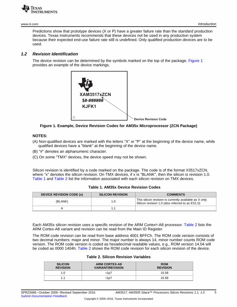
1.2 Revision IdentificationThe device revision can be determined by the symbols marked on the top of the package. Figure 1provides an example of the device markings.
Figure 1. Example, Device Revision Codes for AM35x Microprocessor (ZCN Package)
NOTES:(A) Non-qualified devices are marked with the letters "X" or "P" at the beginning of the device name, while
qualified devices have a "blank" at the beginning of the device name.(B) "#" denotes an alphanumeric character.(C) On some "TMX" devices, the device speed may not be shown.
Silicon revision is identified by a code marked on the package. The code is of the format X3517xZCN,where "x" denotes the silicon revision. On TMX devices, if x is "BLANK", then the silicon is revision 1.0.Table 1 and Table 2 list the information associated with each silicon revision on TMX devices.
Table 1. AM35x Device Revision Codes
DEVICE REVISION CODE (x) SILICON REVISION COMMENTS
(BLANK) 1.0 This silicon revision is currently available as X only.Silicon revision 1.0 (also referred to as ES1.0)
A 1.1
Each AM35x silicon revision uses a specific revision of the ARM Cortex®-A8 processor. Table 2 lists theARM Cortex-A8 variant and revision can be read from the Main ID Register.
The ROM code revision can be read from base address 4001 BFFCh. The ROM code version consists oftwo decimal numbers: major and minor. The major number is always 14, minor number counts ROM codeversion. The ROM code version is coded as hexadecimal readable values, e.g., ROM version 14.04 willbe coded as 0000 1404h. Table 2 shows the ROM code revision for each silicon revision of the device.
Table 2. Silicon Revision Variables
SILICONREVISION
ARM CORTEX-A8VARIANT/REVISION
ROMREVISION
1.0 r1p7 15.581.1 r1p7 15.58
Silicon Revision 1.1 Usage Notes and Known Design Exceptions to Functional Specifications www.ti.com
6 SPRZ306E–October 2009–Revised September 2016Submit Documentation Feedback
Copyright © 2009–2016, Texas Instruments Incorporated
AM3517, AM3505 Sitara™ Processors Silicon Revisions 1.1, 1.0
2 Silicon Revision 1.1 Usage Notes and Known Design Exceptions to FunctionalSpecifications
2.1 Usage Notes for Silicon Revision 1.1Usage Notes highlight and describe particular situations where the device's behavior may not matchpresumed or documented behavior. This may include behaviors that affect device performance orfunctional correctness. These notes will be incorporated into future documentation updates for the device(such as the device-specific data manual), and the behaviors they describe will not be altered in futuresilicon revisions.
Note: The peripherals supported on the various AM35x microprocessors are different. The user shouldonly refer to usage notes and advisories pertaining to features supported on the specific device. For acomplete list of the supported features of the AM35x microprocessors, see the device-specific datamanual.
2.1.1 Cortex-A8 Errata ListThis document does not cover the advisories associated with the Cortex-A8 processor. For a list of theadvisories associated with the each version of the Cortex-A8 processor, contact your TI representative forthe latest copy of the ARM Core Cortex-A8 (AT400/AT401/AT490) Errata Notice. See Table 2 todetermine which version of the Cortex-A8 processor is included in eachAM35x silicon revision.
2.1.2 SGX Errata ListOn the AM35x devices, the SGX is considered to be a "black box" for most users; therefore, no detailedinformation about SGX advisories will be provided in this document. SGX advisories are discussed in theImagination Technologies™ errata, which is available for API/Code Developers only.
2.1.3 Performance Limitation on LCD Read/Write Access Through RFBI L4 PortBack-to-back accesses for both Read and Write to the LCD through the L4 interconnect interface of theRFBI module are not supported. A penalty of 1 L4 clock cycle between two consecutive accesses exists.
Read access to the LCD through the RFBI L4 port: The data of a Read access is sent back to theinitiator of the access only at RECycleTime. RECycleTime is used as a reference event for CS release aswell (CS is used as an on-going access notification signal depending on the type of LCD panelconnected). This means that any Read access to the LCD through the L4 interface of the RFBI will beended by a CS release (CS going inactive at the end of the access). Therefore, the does not support twoconsecutive Read accesses to the LCD (there is always 1 L4 clock cycle between 2 accesses).
Write access to the LCD through the RFBI L4 port: For a Write access, the back-to-back data of asingle access that has been split is supported and guaranteed (e.g., one 32-bit write split in twoconsecutive, back-to-back, 16-bit accesses). In this case, the internal bus CS signal will be kept activeuntil split access completion. However, when there are two different write accesses from the initiator, theywill not be seen as back-to-back by the LCD. At the end of the transaction corresponding to one writeaccess from the initiator, the internal bus CS will be released at WECycleTime, and the next commandfrom the initiator will be accepted. Consequently, any Write access to the LCD through the L4 interface ofthe RFBI will be ended by a CS release (CS going inactive at the end of the access). Therefore, the doesnot support two consecutive data transmits to the LCD (corresponding to two different and consecutiveWrite accesses from the initiator).
www.ti.com Silicon Revision 1.1 Usage Notes and Known Design Exceptions to Functional Specifications
7SPRZ306E–October 2009–Revised September 2016Submit Documentation Feedback
Copyright © 2009–2016, Texas Instruments Incorporated
AM3517, AM3505 Sitara™ Processors Silicon Revisions 1.1, 1.0
2.1.4 VENC: Last Data Line Missing in PALThe VENC cannot show the image data at the end of the even frames on line 623. This is a minorviolation of the ITU-R BT.470-6. Since lines 23 and 336 are reserved for WSS, the VENC can only show574 lines of data instead of the 576 lines defined in the standard. One half line is missing for lines 23(reserved for WSS) and 623, and one full line is missing for line 336 (reserved for WSS).
2.1.5 UART: Cannot Acknowledge Idle Requests in Smartidle Mode When Configured for DMAOperations
When configured for DMA operations using smartidle mode (SYSC[4:3].IDLEMODE = 0x2), the UARTmodule will not acknowledge incoming idle requests. As a consequence, it can prevent L4 from going toidle.
When there are additional expected transfers, the UART should be placed in force-idle mode.
2.1.6 Unexpected RFBI Latency for High Frame RateThe Remote Frame Buffer (RFBI) state machine architecture can create non-optimized pipelining of theRFBI output data stream. As a result, some idle cycles may be inserted between RFBI accesses to theexternal panels. The number of idle cycles added depends on theAM35x clock configuration and RFBIconfiguration. Table 3 shows the minimum additional number of cycles depending on the RFBIconfigurations.
Table 3. Additional Minimum Cycletime (CS/WE Always Asserted)
RFBI PERFORMANCE RFBI_CONFIG.CYCLEFORMAT RFBI_CONFIG. OCPFORMAT MIN CYCLETIME (Number of
OCP cycles)OCP Slave 1 pixel/ cycle 1 pixel 5
1 pixel/ 2 cycles 1 pixel 41 pixel/ 3 cycles 1 pixel 42 pixels/ 3 cycles 1 pixel 6
1 pixel/ cycle 2 pixels 41 pixel/ 2 cycles 2 pixels 41 pixel/ 3 cycles 2 pixels 42 pixels/ 3 cycles 2 pixels 6
Display Controller 1 pixel/ cycle N/A 41 pixel/ 2 cycles N/A 31 pixel/ 3 cycles N/A 31 pixel/ 3 cycles N/A 6
High-speed USBOTG controller
High-speedUSB
host subsystem
Port
1P
ort
2P
ort
3
Device
Port
0
Silicon Revision 1.1 Usage Notes and Known Design Exceptions to Functional Specifications www.ti.com
8 SPRZ306E–October 2009–Revised September 2016Submit Documentation Feedback
Copyright © 2009–2016, Texas Instruments Incorporated
AM3517, AM3505 Sitara™ Processors Silicon Revisions 1.1, 1.0
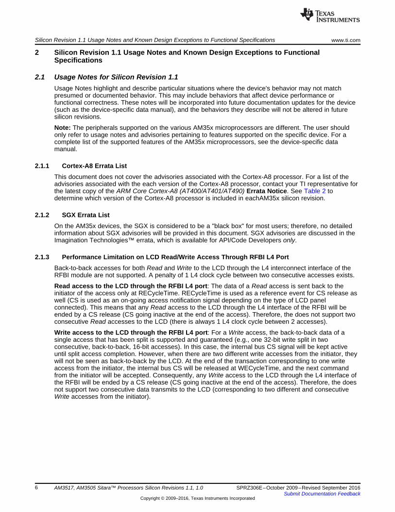
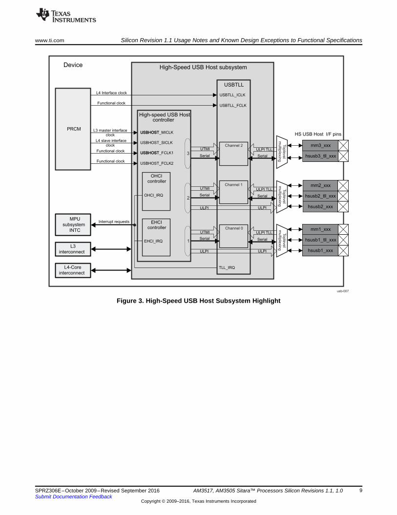
2.1.7 HS USB Host Subsystem: Some Limitations Exist When Connecting to External DevicesAs shown in Figure 2, the device includes a high-speed universal serial bus (USB) OTG controller and ahigh-speed USB host subsystem.
Figure 2. AM35x USB Modules
The high-speed USB OTG controller supports a single USB port which uses a UTMI + interface to connectto the integrated USB OTG PHY.
As shown in Figure 3, the high-speed universal serial bus (USB) host subsystem supports up to threeUSB ports, each one of which can owned by one of two controllers:• The EHCI controller, based on the Enhanced Host Controller Interface (EHCI) specification for USB
Release 1.0, is in charge of high-speed traffic (480M bit/s) over either a UTMI port or a UTMI low-pininterface (ULPI) port.
• The OHCI controller, based on the Open Host Controller Interface (OHCI) specification for USBRelease 1.0a, is in charge of full-speed/low-speed traffic (12/1.5M bit/s, respectively) over a serialinterface.
Please note the following functional limitations when using the high-speed USB host subsystem:• If one port is configured in the ULPI mode, then all other ports must use the same configuration.
Therefore, the ports must be configured high-speed mode or full-speed/low-speed mode. For moreinformation, see ECHI and OHCI Controllers Cannot Work Concurrently.
• USB Port 3 cannot operate in ULPI mode; it can only operate in serial mode.
usb-007
High-Speed USB Host subsystem
High-speed USB Host
MPU
subsystem
INTC
mm2_xxx
OHCIcontroller
OHCI_IRQ
EHCI_IRQ
hsusb2_tll_xxx
hsusb2_xxx
hsusb1_tll_xxx
hsusb1_xxxL3
interconnect
L4-Core
interconnect
Device
Interrupt requests
USBHOSTUSBHOST_MICLK HS USB Host I/F pins
USBHOST_SICLK
TLL_IRQ
L3 master interface
L4 slave interface
USBHOSTUSBHOST_FCLK1
USBHOST_FCLK2
EHCIcontroller
ULPI TLL
Serial
ULPI TLL
Serial
ULPI TLL
Serial
Channel 2
Channel 1
Channel 0
USBTLL
Serial
Serial
Serial
UTMI
UTMI
UTMI
clock
clock
Functional clock
Functional clock
controller
3
2
1
To
ple
ve
lm
ultip
lexin
gTo
ple
ve
lm
ultip
lexin
gTo
ple
ve
lm
ultip
lexin
g
mm1_xxx
hsusb3_tll_xxx
mm3_xxx
ULPI
ULPI
ULPI
ULPI
PRCM
USBTLL_ICLK
USBTLL_FCLKFunctional clock
L4 Interface clock
www.ti.com Silicon Revision 1.1 Usage Notes and Known Design Exceptions to Functional Specifications
9SPRZ306E–October 2009–Revised September 2016Submit Documentation Feedback
Copyright © 2009–2016, Texas Instruments Incorporated
AM3517, AM3505 Sitara™ Processors Silicon Revisions 1.1, 1.0
Figure 3. High-Speed USB Host Subsystem Highlight
ULPI HS
PHY(A)
Device
Po
rt 1 12-pin ULPI
(Device Outputs Clock)
Po
rt 2 12-pin ULPI
( Outputs Clock)Device
Po
rt 3
Not Used
Not Used
A. USB port 3 does not support ULPI mode.
HS USBHUB
HS/FS/LSDevice or
Receptacle
HS/FS/LSDevice or
Receptacle
HS/FS/LSDevice or
Receptacle
ULPI HS
PHY(A)
Device
HS
Ho
st
Co
ntr
oller
(EH
CI)
Po
rt 1 12-pin ULPI
(Device Outputs Clock)
Po
rt 2 12-pin ULPI
(Device Outputs Clock)P
ort
3
Not Used
ULPI HS
PHY(A)
A. USB port 3 does not support ULPI mode.
Silicon Revision 1.1 Usage Notes and Known Design Exceptions to Functional Specifications www.ti.com
10 SPRZ306E–October 2009–Revised September 2016Submit Documentation Feedback
Copyright © 2009–2016, Texas Instruments Incorporated
AM3517, AM3505 Sitara™ Processors Silicon Revisions 1.1, 1.0
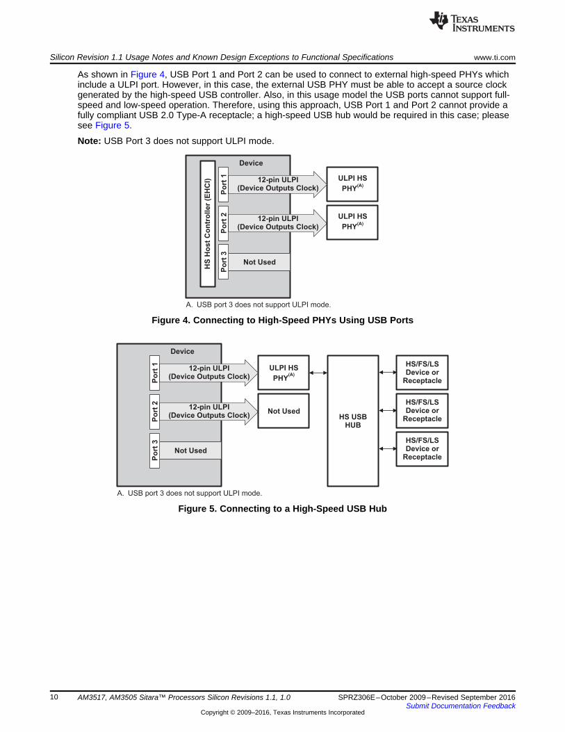
As shown in Figure 4, USB Port 1 and Port 2 can be used to connect to external high-speed PHYs whichinclude a ULPI port. However, in this case, the external USB PHY must be able to accept a source clockgenerated by the high-speed USB controller. Also, in this usage model the USB ports cannot support full-speed and low-speed operation. Therefore, using this approach, USB Port 1 and Port 2 cannot provide afully compliant USB 2.0 Type-A receptacle; a high-speed USB hub would be required in this case; pleasesee Figure 5.
Note: USB Port 3 does not support ULPI mode.
Figure 4. Connecting to High-Speed PHYs Using USB Ports
Figure 5. Connecting to a High-Speed USB Hub
www.ti.com Silicon Revision 1.1 Usage Notes and Known Design Exceptions to Functional Specifications
11SPRZ306E–October 2009–Revised September 2016Submit Documentation Feedback
Copyright © 2009–2016, Texas Instruments Incorporated
AM3517, AM3505 Sitara™ Processors Silicon Revisions 1.1, 1.0
2.2 Silicon Revision 1.1 Known Design Exceptions to Functional Specifications
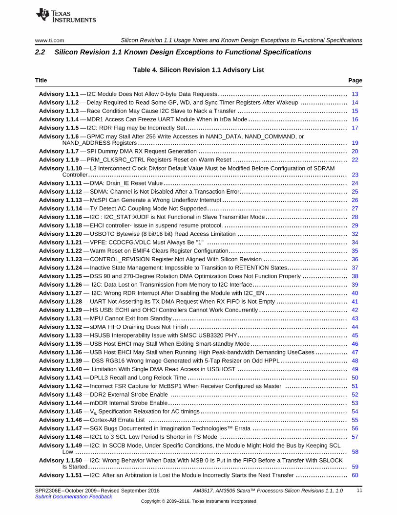
Table 4. Silicon Revision 1.1 Advisory ListTitle ...................................................................................................................................... Page
Advisory 1.1.1 —I2C Module Does Not Allow 0-byte Data Requests ............................................................ 13Advisory 1.1.2 —Delay Required to Read Some GP, WD, and Sync Timer Registers After Wakeup ...................... 14Advisory 1.1.3 —Race Condition May Cause I2C Slave to Nack a Transfer ................................................... 15Advisory 1.1.4 —MDR1 Access Can Freeze UART Module When in IrDa Mode .............................................. 16Advisory 1.1.5 —I2C: RDR Flag may be Incorrectly Set........................................................................... 17Advisory 1.1.6 —GPMC may Stall After 256 Write Accesses in NAND_DATA, NAND_COMMAND, or
NAND_ADDRESS Registers ................................................................................................. 19Advisory 1.1.7 —SPI Dummy DMA RX Request Generation ..................................................................... 20Advisory 1.1.9 —PRM_CLKSRC_CTRL Registers Reset on Warm Reset ..................................................... 22Advisory 1.1.10 —L3 Interconnect Clock Divisor Default Value Must be Modified Before Configuration of SDRAM
Controller........................................................................................................................ 23Advisory 1.1.11 —DMA: Drain_IE Reset Value ..................................................................................... 24Advisory 1.1.12 —SDMA: Channel is Not Disabled After a Transaction Error.................................................. 25Advisory 1.1.13 —McSPI Can Generate a Wrong Underflow Interrupt .......................................................... 26Advisory 1.1.14 —TV Detect AC Coupling Mode Not Supported................................................................. 27Advisory 1.1.16 —I2C : I2C_STAT:XUDF is Not Functional in Slave Transmitter Mode...................................... 28Advisory 1.1.18 —EHCI controller- Issue in suspend resume protocol. ......................................................... 29Advisory 1.1.20 —USBOTG Bytewise (8 bit/16 bit) Read Access Limitation ................................................... 32Advisory 1.1.21 —VPFE: CCDCFG.VDLC Must Always Be "1" ................................................................. 34Advisory 1.1.22 —Warm Reset on EMIF4 Clears Register Configuration....................................................... 35Advisory 1.1.23 —CONTROL_REVISION Register Not Aligned With Silicon Revision ....................................... 36Advisory 1.1.24 —Inactive State Management: Impossible to Transition to RETENTION States............................ 37Advisory 1.1.25 —DSS 90 and 270-Degree Rotation DMA Optimization Does Not Function Properly ..................... 38Advisory 1.1.26 — I2C: Data Lost on Transmission from Memory to I2C Interface............................................ 39Advisory 1.1.27 — I2C: Wrong RDR Interrupt After Disabling the Module with I2C_EN ...................................... 40Advisory 1.1.28 —UART Not Asserting its TX DMA Request When RX FIFO is Not Empty ................................. 41Advisory 1.1.29 —HS USB: ECHI and OHCI Controllers Cannot Work Concurrently ......................................... 42Advisory 1.1.31 —MPU Cannot Exit from Standby................................................................................. 43Advisory 1.1.32 —sDMA FIFO Draining Does Not Finish ......................................................................... 44Advisory 1.1.33 —HSUSB Interoperability Issue with SMSC USB3320 PHY................................................... 45Advisory 1.1.35 —USB Host EHCI may Stall When Exiting Smart-standby Mode............................................. 46Advisory 1.1.36 —USB Host EHCI May Stall when Running High Peak-bandwidth Demanding UseCases ............... 47Advisory 1.1.39 — DSS RGB16 Wrong Image Generated with 5-Tap Resizer on Odd HPPL ............................... 48Advisory 1.1.40 — Limitation With Single DMA Read Access in USBHOST ................................................... 49Advisory 1.1.41 —DPLL3 Recall and Long Relock Time .......................................................................... 50Advisory 1.1.42 —Incorrect FSR Capture for McBSP1 When Receiver Configured as Master ............................. 51Advisory 1.1.43 —DDR2 External Strobe Enable .................................................................................. 52Advisory 1.1.44 —mDDR Internal Strobe Enable................................................................................... 53Advisory 1.1.45 —VIL Specification Relaxation for AC timings .................................................................... 54Advisory 1.1.46 —Cortex-A8 Errata List ............................................................................................ 55Advisory 1.1.47 —SGX Bugs Documented in Imagination Technologies™ Errata ............................................ 56Advisory 1.1.48 —I2C1 to 3 SCL Low Period Is Shorter in FS Mode ........................................................... 57Advisory 1.1.49 —I2C: In SCCB Mode, Under Specific Conditions, the Module Might Hold the Bus by Keeping SCL
Low .............................................................................................................................. 58Advisory 1.1.50 —I2C: Wrong Behavior When Data With MSB 0 Is Put in the FIFO Before a Transfer With SBLOCK
Is Started........................................................................................................................ 59Advisory 1.1.51 —I2C: After an Arbitration is Lost the Module Incorrectly Starts the Next Transfer ........................ 60
Silicon Revision 1.1 Usage Notes and Known Design Exceptions to Functional Specifications www.ti.com
12 SPRZ306E–October 2009–Revised September 2016Submit Documentation Feedback
Copyright © 2009–2016, Texas Instruments Incorporated
AM3517, AM3505 Sitara™ Processors Silicon Revisions 1.1, 1.0
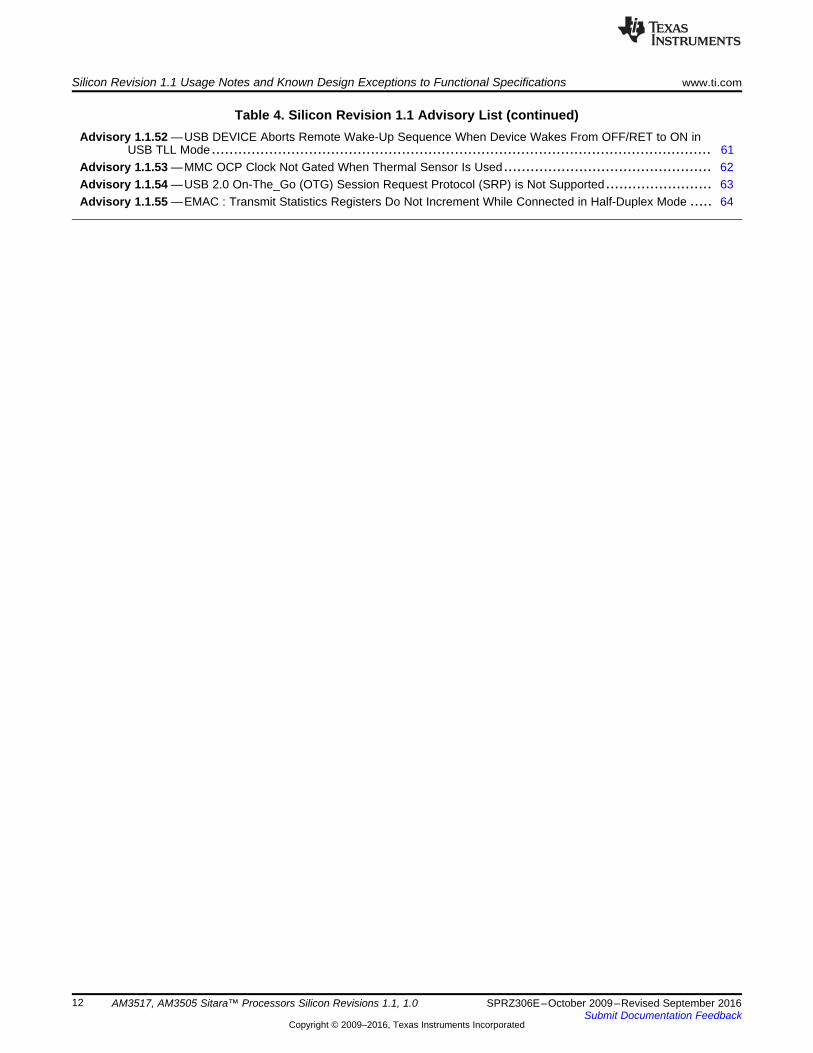
Table 4. Silicon Revision 1.1 Advisory List (continued)Advisory 1.1.52 —USB DEVICE Aborts Remote Wake-Up Sequence When Device Wakes From OFF/RET to ON in
USB TLL Mode ................................................................................................................. 61Advisory 1.1.53 —MMC OCP Clock Not Gated When Thermal Sensor Is Used............................................... 62Advisory 1.1.54 —USB 2.0 On-The_Go (OTG) Session Request Protocol (SRP) is Not Supported........................ 63Advisory 1.1.55 —EMAC : Transmit Statistics Registers Do Not Increment While Connected in Half-Duplex Mode ..... 64

www.ti.com Silicon Revision 1.1 Usage Notes and Known Design Exceptions to Functional Specifications
13SPRZ306E–October 2009–Revised September 2016Submit Documentation Feedback
Copyright © 2009–2016, Texas Instruments Incorporated
AM3517, AM3505 Sitara™ Processors Silicon Revisions 1.1, 1.0
Advisory 1.1.1 I2C Module Does Not Allow 0-byte Data Requests
Revision(s) Affected 1.1 and earlier
Details When configured as the master, the I2C module does not allow 0-byte data transfers.
Note: Programming I2Ci.I2C_CNT[15:0]: DCOUNT = 0 will cause undefined behavior.
Workaround(s) No workaround. Do not use 0-byte data requests.
Silicon Revision 1.1 Usage Notes and Known Design Exceptions to Functional Specifications www.ti.com
14 SPRZ306E–October 2009–Revised September 2016Submit Documentation Feedback
Copyright © 2009–2016, Texas Instruments Incorporated
AM3517, AM3505 Sitara™ Processors Silicon Revisions 1.1, 1.0
Advisory 1.1.2 Delay Required to Read Some GP, WD, and Sync Timer Registers After Wakeup
Revision(s) Affected 1.1 and earlier
Details If a General Purpose Timer (GPTimer) is in posted mode (TSIRC.POSTED = 1), due tointernal resynchronizations, any values read in TCRR, TCAR1, and TCAR2 registersimmediately after the timer interface clock (L4) goes from a stopped state to an activestate may not return the expected values. This situation is most likely when the wakesup from an idle state.
Notes:• GPTimer non-posted synchronization mode is not impacted by this advisory.• This advisory also impacts reads from Watchdog timers WCRR registers.• All of the watchdog timers support only posted internal synchronization mode. There
is no capability to change the internal synchronization scheme to non-posted modevia software.
• The 32K sync timer CR and 32SYNCNT_REV registers are also impacted by thisadvisory, since the 32K sync timer is always in posted synchronization mode.
Workaround(s) The software must wait at least 2 timer interface clock cycles + 1 timer functional clockcycle after L4 clock-wakeup before reading TCRR, TCAR1, or TCAR2 registers for GPTimers in posted internal synchronization mode, and before reading the WCRR registerof the Watchdog timers. The same workaround must be applied before reading CR and32KSYNCNT_REV registers of the synctimer module.
www.ti.com Silicon Revision 1.1 Usage Notes and Known Design Exceptions to Functional Specifications
15SPRZ306E–October 2009–Revised September 2016Submit Documentation Feedback
Copyright © 2009–2016, Texas Instruments Incorporated
AM3517, AM3505 Sitara™ Processors Silicon Revisions 1.1, 1.0
Advisory 1.1.3 Race Condition May Cause I2C Slave to Nack a Transfer
Revision(s) Affected 1.1 and earlier
Details If the I2C module is configured as a slave, in autoidle mode (I2C_SYSC.AUTOIDLE = 1)and the ARDY (I2C.12C_STAT[2]) condition and the START condition are detected inthe module at the same time, internal clock gating will be incorrectly applied. This willcause the I2C to NACK (I2C.12C_STAT[1]) the transfer for which the START(I2C.I2C_STA[6]) condition was received. Subsequent transfers will be ACKed asexpected.
Workaround(s) Workaround 1: Software must set SYSC_AUTOIDLE to 0. In this case, the failurecondition never occurs.
Workaround 2: Ensure that the external I2C master always resends a NACKed transfervia software. If a transfer was NACKed because of this race condition, the next transferwill always be ACKed.
Silicon Revision 1.1 Usage Notes and Known Design Exceptions to Functional Specifications www.ti.com
16 SPRZ306E–October 2009–Revised September 2016Submit Documentation Feedback
Copyright © 2009–2016, Texas Instruments Incorporated
AM3517, AM3505 Sitara™ Processors Silicon Revisions 1.1, 1.0
Advisory 1.1.4 MDR1 Access Can Freeze UART Module When in IrDa Mode
Revision(s) Affected 1.1 and earlier
Details Because of a glitchy structure inside the UART module, accessing the MDR1 registermay create a dummy underrun condition and freeze the UART IrDa transmission. OnlyIrDa modes Slow Infrared (SIR), Medium Infrared (MIR), and Fast Infrared (FIR) areimpacted. Even if the bug condition occurs in UART mode or IrDa CIR mode, it will haveno effect. Therefore, UART1 and UART2 are immune to this problem, and only UART3may exhibit this issue when used in one of the IrDa modes– SIR, MIR, or FIR.
Workaround(s) To ensure this problem does not occur, the following software initialization sequencemust be used each time MDR1 must be changed to one of the three failing IrDa modes:1. If needed, setup the UART by writing the required registers, except MDR1.2. Set appropriately the MDR1.MODE_SELECT bit field.3. Wait for 5 L4 clock cycles + 5 UART functional clock cycles.4. Read RESUME register to resume the halted operation.

www.ti.com Silicon Revision 1.1 Usage Notes and Known Design Exceptions to Functional Specifications
17SPRZ306E–October 2009–Revised September 2016Submit Documentation Feedback
Copyright © 2009–2016, Texas Instruments Incorporated
AM3517, AM3505 Sitara™ Processors Silicon Revisions 1.1, 1.0
Advisory 1.1.5 I2C: RDR Flag may be Incorrectly Set
Revision(s) Affected 1.1 and earlier
Details Under certain rare conditions, the I2C_STAT[13].RDR bit may be set as well as thecorresponding interrupt fire, even when there is no data in the receive FIFO, or the I2Cdata transfer is still ongoing. These spurious RDR events must be ignored by thesoftware.
Workaround(s) Software must filter out unexpected RDR pulses, using the flowchart illustrated inFigure 6 when receiving an I2C RDR interrupt.
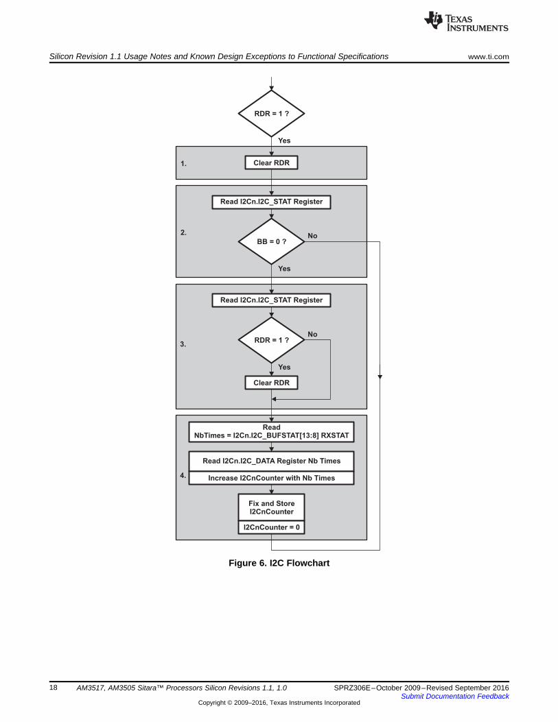
3.
ReadNbTimes = I2Cn.I2C_BUFSTAT[13:8] RXSTAT
Read I2Cn.I2C_DATA Register Nb Times
Increase I2CnCounter with Nb Times
Fix and StoreI2CnCounter
I2CnCounter = 0
4.
RDR = 1 ?
Clear RDR
No
Yes
Read I2Cn.I2C_STAT Register
BB = 0 ?No
Yes
Read I2Cn.I2C_STAT Register
2.
Clear RDR
RDR = 1 ?
Yes
1.
Silicon Revision 1.1 Usage Notes and Known Design Exceptions to Functional Specifications www.ti.com
18 SPRZ306E–October 2009–Revised September 2016Submit Documentation Feedback
Copyright © 2009–2016, Texas Instruments Incorporated
AM3517, AM3505 Sitara™ Processors Silicon Revisions 1.1, 1.0
Figure 6. I2C Flowchart
www.ti.com Silicon Revision 1.1 Usage Notes and Known Design Exceptions to Functional Specifications
19SPRZ306E–October 2009–Revised September 2016Submit Documentation Feedback
Copyright © 2009–2016, Texas Instruments Incorporated
AM3517, AM3505 Sitara™ Processors Silicon Revisions 1.1, 1.0
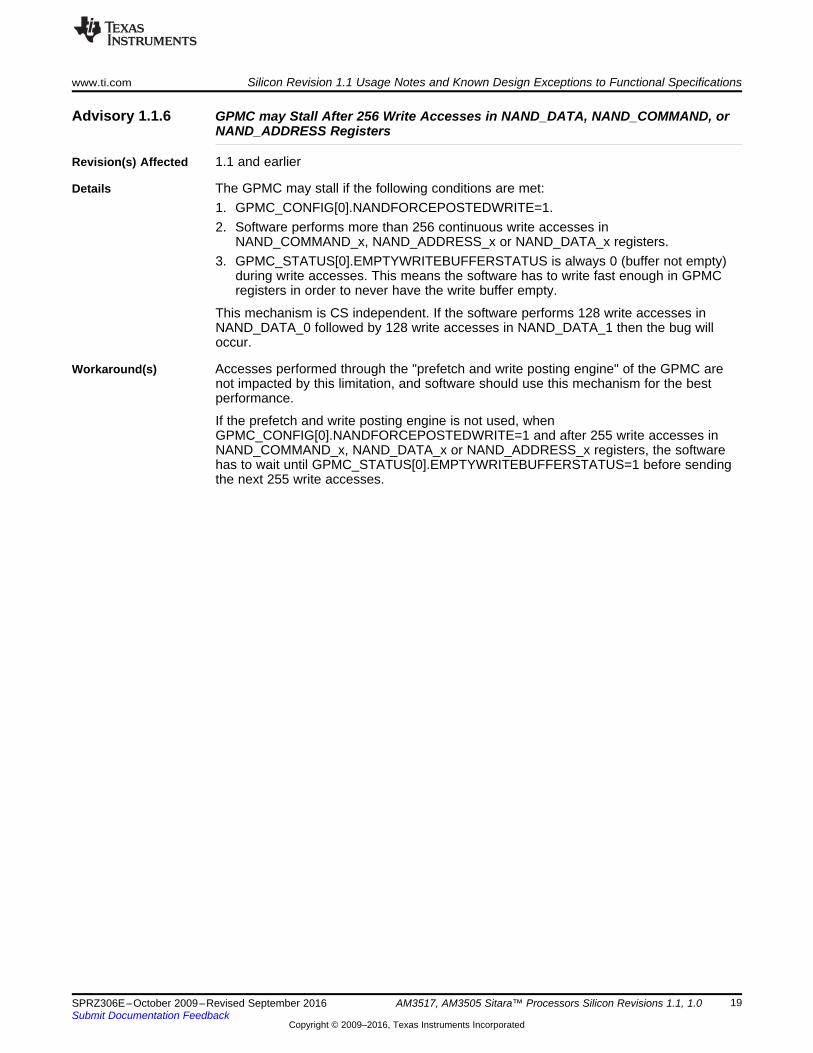
Advisory 1.1.6 GPMC may Stall After 256 Write Accesses in NAND_DATA, NAND_COMMAND, orNAND_ADDRESS Registers
Revision(s) Affected 1.1 and earlier
Details The GPMC may stall if the following conditions are met:1. GPMC_CONFIG[0].NANDFORCEPOSTEDWRITE=1.2. Software performs more than 256 continuous write accesses in
NAND_COMMAND_x, NAND_ADDRESS_x or NAND_DATA_x registers.3. GPMC_STATUS[0].EMPTYWRITEBUFFERSTATUS is always 0 (buffer not empty)
during write accesses. This means the software has to write fast enough in GPMCregisters in order to never have the write buffer empty.
This mechanism is CS independent. If the software performs 128 write accesses inNAND_DATA_0 followed by 128 write accesses in NAND_DATA_1 then the bug willoccur.
Workaround(s) Accesses performed through the "prefetch and write posting engine" of the GPMC arenot impacted by this limitation, and software should use this mechanism for the bestperformance.
If the prefetch and write posting engine is not used, whenGPMC_CONFIG[0].NANDFORCEPOSTEDWRITE=1 and after 255 write accesses inNAND_COMMAND_x, NAND_DATA_x or NAND_ADDRESS_x registers, the softwarehas to wait until GPMC_STATUS[0].EMPTYWRITEBUFFERSTATUS=1 before sendingthe next 255 write accesses.
SPI RX DMARequest
SPI CS
SPI CLK
2–SPI Slave Configuration
4–Enable Slave, then Master. No DummyDMA Request Generated (No Previous CLKFalling Edge)
3–SPI Master Configuration (CLK Driven Low)
1–SPI Pin Muxing Configuration (CLK Pulled Down, CS Pulled Down)
SPI RX DMARequest
SPI CS
SPI CLK
2–SPI Slave Configuration
4–Enable Slave, then Master. Dummy DMARequest is Generated Because of PreviousCLK Falling
3–SPI Master Configuration (CLK Driven Low)
1–SPI Pin Muxing Configuration (CLK Pulled Up, CS Pulled Down)
Silicon Revision 1.1 Usage Notes and Known Design Exceptions to Functional Specifications www.ti.com
20 SPRZ306E–October 2009–Revised September 2016Submit Documentation Feedback
Copyright © 2009–2016, Texas Instruments Incorporated
AM3517, AM3505 Sitara™ Processors Silicon Revisions 1.1, 1.0
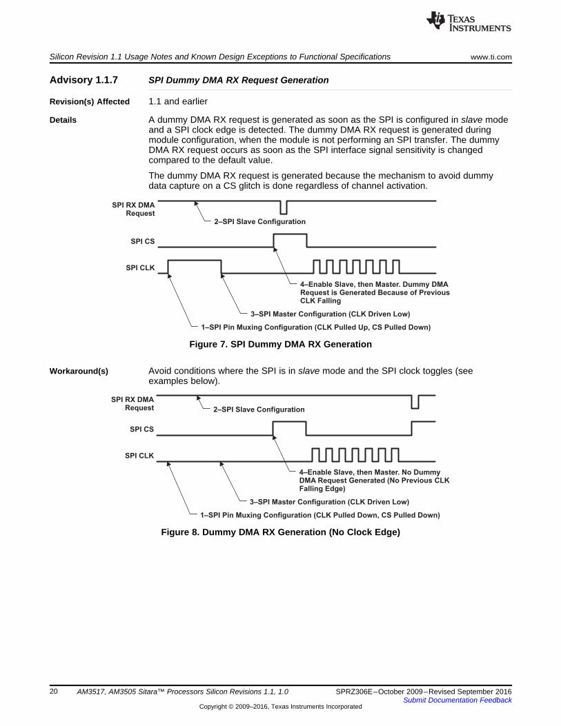
Advisory 1.1.7 SPI Dummy DMA RX Request Generation
Revision(s) Affected 1.1 and earlier
Details A dummy DMA RX request is generated as soon as the SPI is configured in slave modeand a SPI clock edge is detected. The dummy DMA RX request is generated duringmodule configuration, when the module is not performing an SPI transfer. The dummyDMA RX request occurs as soon as the SPI interface signal sensitivity is changedcompared to the default value.
The dummy DMA RX request is generated because the mechanism to avoid dummydata capture on a CS glitch is done regardless of channel activation.
Figure 7. SPI Dummy DMA RX Generation
Workaround(s) Avoid conditions where the SPI is in slave mode and the SPI clock toggles (seeexamples below).
Figure 8. Dummy DMA RX Generation (No Clock Edge)
SPI RX DMARequest
SPI CS
SPI CLK
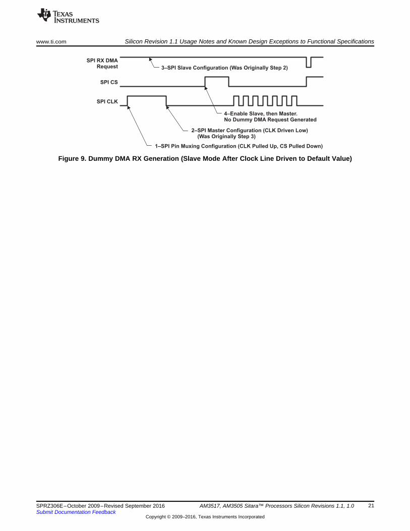
3–SPI Slave Configuration (Was Originally Step 2)
4–Enable Slave, then Master.No Dummy DMA Request Generated
2–SPI Master Configuration (CLK Driven Low)(Was Originally Step 3)
1–SPI Pin Muxing Configuration (CLK Pulled Up, CS Pulled Down)
www.ti.com Silicon Revision 1.1 Usage Notes and Known Design Exceptions to Functional Specifications
21SPRZ306E–October 2009–Revised September 2016Submit Documentation Feedback
Copyright © 2009–2016, Texas Instruments Incorporated
AM3517, AM3505 Sitara™ Processors Silicon Revisions 1.1, 1.0
Figure 9. Dummy DMA RX Generation (Slave Mode After Clock Line Driven to Default Value)
Silicon Revision 1.1 Usage Notes and Known Design Exceptions to Functional Specifications www.ti.com
22 SPRZ306E–October 2009–Revised September 2016Submit Documentation Feedback
Copyright © 2009–2016, Texas Instruments Incorporated
AM3517, AM3505 Sitara™ Processors Silicon Revisions 1.1, 1.0
Advisory 1.1.9 PRM_CLKSRC_CTRL Registers Reset on Warm Reset
Revision(s) Affected 1.1 and earlier
Details The PRM_CLKSRC_CTRL registers are reset on a Warm Reset; however, they shouldbe reset on Cold Reset only. These parameters depend on the device environment only,but the registers must be re-programmed.
Workaround(s) If the default values are not used, the registers must be reprogrammed after warm resetis released.
www.ti.com Silicon Revision 1.1 Usage Notes and Known Design Exceptions to Functional Specifications
23SPRZ306E–October 2009–Revised September 2016Submit Documentation Feedback
Copyright © 2009–2016, Texas Instruments Incorporated
AM3517, AM3505 Sitara™ Processors Silicon Revisions 1.1, 1.0
Advisory 1.1.10 L3 Interconnect Clock Divisor Default Value Must be Modified BeforeConfiguration of SDRAM Controller
Revision(s) Affected 1.1 and earlier
Details The SDRAM output clock is gated when an incorrect L3 CLK_SEL ratio is set. Thisoperation is generally transparent and handled at boot time by the ROM code. Theworkaround should be implemented for the following scenarios:• GP device External Fast boot is used.
Workaround(s) For External Fast Boot which are both impacted by the issue, CLKSEL_L3 (bits 1:0) =10b must be set before performing SDRC configuration. In all other cases, thisprograming is handled by the ROM code and no workaround is necessary.
Silicon Revision 1.1 Usage Notes and Known Design Exceptions to Functional Specifications www.ti.com
24 SPRZ306E–October 2009–Revised September 2016Submit Documentation Feedback
Copyright © 2009–2016, Texas Instruments Incorporated
AM3517, AM3505 Sitara™ Processors Silicon Revisions 1.1, 1.0
Advisory 1.1.11 DMA: Drain_IE Reset Value
Revision(s) Affected 1.1 and earlier
Details The Drain_IE bit in the DMA4_CICRi[12] register is not initialized after POR; its defaultvalue can be either '0' or '1' while the documentation specifies '0'.
Workaround(s) Prior to the DMA setup, the software must write 0x0 to this bit to disable the Drain_IEinterrupt in the CICR register.
www.ti.com Silicon Revision 1.1 Usage Notes and Known Design Exceptions to Functional Specifications
25SPRZ306E–October 2009–Revised September 2016Submit Documentation Feedback
Copyright © 2009–2016, Texas Instruments Incorporated
AM3517, AM3505 Sitara™ Processors Silicon Revisions 1.1, 1.0
Advisory 1.1.12 SDMA: Channel is Not Disabled After a Transaction Error
Revision(s) Affected 1.1 and earlier
Details During a destination synchronized transfer on the write port (or source sync withSDMA.DMA4_CCRin[25] BUFFERING_DISABLE = 1), if a transaction error is reportedat the last element of the transaction, the channel is not automatically disabled by theDMA.
Workaround(s) Whenever a transaction error is detected on the write side of the channel, the softwaremust disable the channel by writing a '0' to DMA4_CCRi[7]: ENABLE bit.

Silicon Revision 1.1 Usage Notes and Known Design Exceptions to Functional Specifications www.ti.com
26 SPRZ306E–October 2009–Revised September 2016Submit Documentation Feedback
Copyright © 2009–2016, Texas Instruments Incorporated
AM3517, AM3505 Sitara™ Processors Silicon Revisions 1.1, 1.0
Advisory 1.1.13 McSPI Can Generate a Wrong Underflow Interrupt
Revision(s) Affected 1.1 and earlier
Details In the case where:• A McSPI module is configured as master and is connected to another McSPI module
configured as a slave (on the same chip, or on a different chip)• The CS polarity is changed from the reset state (i.e., changed from CS inactive low to
CS inactive high) on the master and slave sides• The slave is enabled and then the master is enabled according to the programming
guide
then the slave McSPI will generate a false underflow as soon as the first channel isenabled on the master McSPI side. This is because the master McSPI sets the rightclock and chip select polarities only when the first channel is enabled. As the CS polarityis changed on the master side, this will generate a low-to-high transition on the CSsignal. The slave McSPI will detect this transition and will try to load its shift register,which will result in an underflow interrupt being generated because there is no data toload.
If the slave is an external SPI device, then there is no issue. Only slave McSPI moduleswill be impacted.
If the CS polarity is not changed from its reset state, then there is no issue.
This issue will only occur when performing loopback tests on the same chip between twoMcSPI modules or when communicating through SPI between two McSPI modules on 2different chips.
Workaround(s) The following initialization sequence will solve this issue:1. On the master side: Set MCSPI_MODULCTRL:SINGLE. Perform the following 3
steps by doing 3 different OCP accesses:• Configure channel I in MCSPI_CH(I)_CONF• Set MCSPI_CH(I)_CONF:FORCE• Reset MCSPI_CH(I)_CONF:FORCE• Reset MCSPI_MODULCTRL:SINGLE bit. The SPI bus polarity is now updated.
2. On the slave side : Configure channel 0 : write MCSPI_CH0_CONF Enable channel0 : set MCSPI_CH0_CTRL:EN
3. On the master side : Enable channel I : set MCSPI_CH(I)_CTRL:EN

www.ti.com Silicon Revision 1.1 Usage Notes and Known Design Exceptions to Functional Specifications
27SPRZ306E–October 2009–Revised September 2016Submit Documentation Feedback
Copyright © 2009–2016, Texas Instruments Incorporated
AM3517, AM3505 Sitara™ Processors Silicon Revisions 1.1, 1.0
Advisory 1.1.14 TV Detect AC Coupling Mode Not Supported
Revision(s) Affected 1.1 and earlier
Details The TV detect in AC coupling mode is not implemented accurately and is not functional;therefore, TV detection in AC mode is impossible.
Workaround(s) Use DC coupling mode only.
Silicon Revision 1.1 Usage Notes and Known Design Exceptions to Functional Specifications www.ti.com
28 SPRZ306E–October 2009–Revised September 2016Submit Documentation Feedback
Copyright © 2009–2016, Texas Instruments Incorporated
AM3517, AM3505 Sitara™ Processors Silicon Revisions 1.1, 1.0
Advisory 1.1.16 I2C : I2C_STAT:XUDF is Not Functional in Slave Transmitter Mode
Revision(s) Affected 1.1 and earlier
Details When configured in slave transmitter mode, the I2C_STAT:XUDF will not be set asexpected if an underflow occurs. Only slave transmitter mode is impacted. Mastertransmitter mode is not impacted. The impact is rather low as the user can rely onI2C_STAT:XRDY interrupt status bit instead.
Workaround(s) Use the I2C_STAT:XRDY interrupt bit instead of XUDF when in slave transmitter mode.
www.ti.com Silicon Revision 1.1 Usage Notes and Known Design Exceptions to Functional Specifications
29SPRZ306E–October 2009–Revised September 2016Submit Documentation Feedback
Copyright © 2009–2016, Texas Instruments Incorporated
AM3517, AM3505 Sitara™ Processors Silicon Revisions 1.1, 1.0
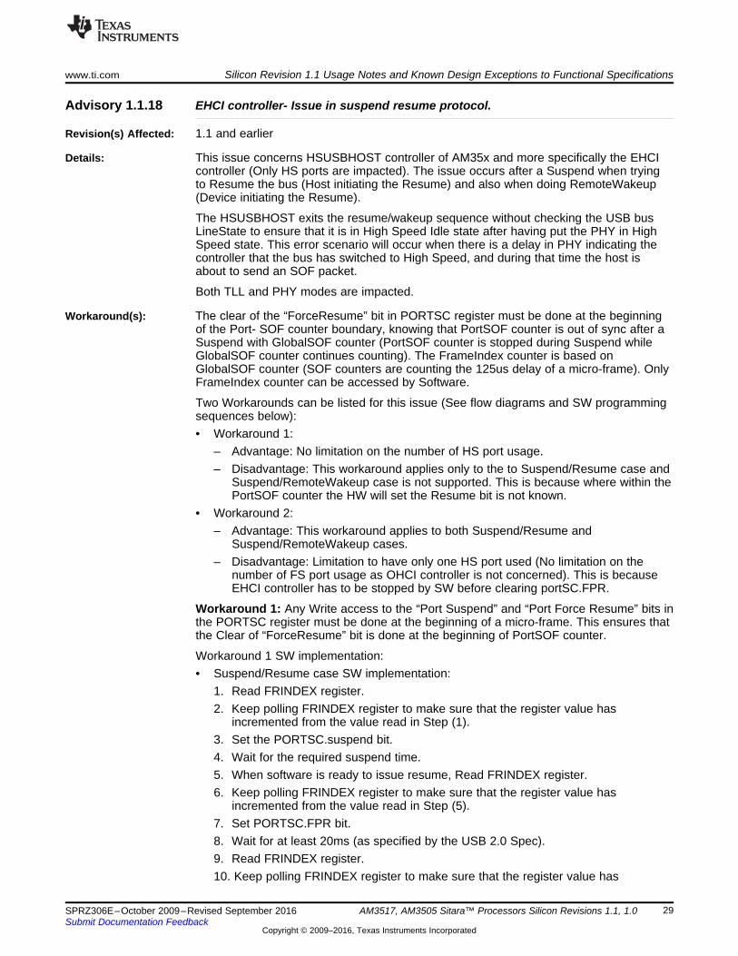
Advisory 1.1.18 EHCI controller- Issue in suspend resume protocol.
Revision(s) Affected: 1.1 and earlier
Details: This issue concerns HSUSBHOST controller of AM35x and more specifically the EHCIcontroller (Only HS ports are impacted). The issue occurs after a Suspend when tryingto Resume the bus (Host initiating the Resume) and also when doing RemoteWakeup(Device initiating the Resume).
The HSUSBHOST exits the resume/wakeup sequence without checking the USB busLineState to ensure that it is in High Speed Idle state after having put the PHY in HighSpeed state. This error scenario will occur when there is a delay in PHY indicating thecontroller that the bus has switched to High Speed, and during that time the host isabout to send an SOF packet.
Both TLL and PHY modes are impacted.
Workaround(s): The clear of the “ForceResume” bit in PORTSC register must be done at the beginningof the Port- SOF counter boundary, knowing that PortSOF counter is out of sync after aSuspend with GlobalSOF counter (PortSOF counter is stopped during Suspend whileGlobalSOF counter continues counting). The FrameIndex counter is based onGlobalSOF counter (SOF counters are counting the 125us delay of a micro-frame). OnlyFrameIndex counter can be accessed by Software.
Two Workarounds can be listed for this issue (See flow diagrams and SW programmingsequences below):• Workaround 1:
– Advantage: No limitation on the number of HS port usage.– Disadvantage: This workaround applies only to the to Suspend/Resume case and
Suspend/RemoteWakeup case is not supported. This is because where within thePortSOF counter the HW will set the Resume bit is not known.
• Workaround 2:– Advantage: This workaround applies to both Suspend/Resume and
Suspend/RemoteWakeup cases.– Disadvantage: Limitation to have only one HS port used (No limitation on the
number of FS port usage as OHCI controller is not concerned). This is becauseEHCI controller has to be stopped by SW before clearing portSC.FPR.
Workaround 1: Any Write access to the “Port Suspend” and “Port Force Resume” bits inthe PORTSC register must be done at the beginning of a micro-frame. This ensures thatthe Clear of “ForceResume” bit is done at the beginning of PortSOF counter.
Workaround 1 SW implementation:• Suspend/Resume case SW implementation:
1. Read FRINDEX register.2. Keep polling FRINDEX register to make sure that the register value has
incremented from the value read in Step (1).3. Set the PORTSC.suspend bit.4. Wait for the required suspend time.5. When software is ready to issue resume, Read FRINDEX register.6. Keep polling FRINDEX register to make sure that the register value has
incremented from the value read in Step (5).7. Set PORTSC.FPR bit.8. Wait for at least 20ms (as specified by the USB 2.0 Spec).9. Read FRINDEX register.10. Keep polling FRINDEX register to make sure that the register value has
Suspend
Set PortSC.Suspend
Host Resume
Set PortSC.Resume
Clear PortSC.Resume
Without Workaround
Wait Until FrameIndexIncrements
Set PortSC.Suspend
Set PortSC.Resume
Wait 20 ms
Clear PortSC.Resume
- LocalSOF and GlobalSOF counters are in sync.
Wait FrameIndexIncrementsUntil
Wait FrameIndexIncrementsUntil
SuspendSuspend
Host Resume
Without Workaround
(FrameIndex Increments Every 124 µs)
- It is ensured that Resume bit is cleared
near start of LocalSOF counter.
- LocalSOF (port-related SOF) counter startscounting from the frozen value.
- GlobalSOF and LocalSOF boundaries arealmost in sync.
Wait 20 ms
- LocalSOF (port-related SOF) counter freezesnear start of LocalSOF boundary.
- GlobalSOF counter continues counting.
Host decides to Resume the port.
Silicon Revision 1.1 Usage Notes and Known Design Exceptions to Functional Specifications www.ti.com
30 SPRZ306E–October 2009–Revised September 2016Submit Documentation Feedback
Copyright © 2009–2016, Texas Instruments Incorporated
AM3517, AM3505 Sitara™ Processors Silicon Revisions 1.1, 1.0
incremented from the value read in Step (9).11. Clear PORTSC.FPR bit.
Figure 10. Workaround 1 Implementation Diagram
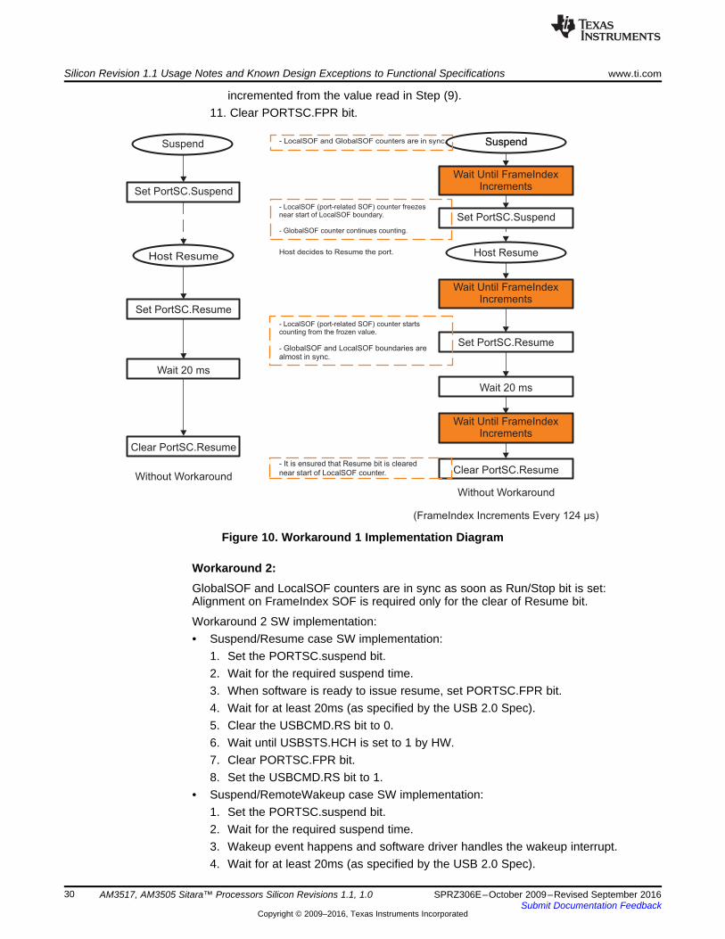
Workaround 2:GlobalSOF and LocalSOF counters are in sync as soon as Run/Stop bit is set:Alignment on FrameIndex SOF is required only for the clear of Resume bit.
Workaround 2 SW implementation:• Suspend/Resume case SW implementation:
1. Set the PORTSC.suspend bit.2. Wait for the required suspend time.3. When software is ready to issue resume, set PORTSC.FPR bit.4. Wait for at least 20ms (as specified by the USB 2.0 Spec).5. Clear the USBCMD.RS bit to 0.6. Wait until USBSTS.HCH is set to 1 by HW.7. Clear PORTSC.FPR bit.8. Set the USBCMD.RS bit to 1.
• Suspend/RemoteWakeup case SW implementation:1. Set the PORTSC.suspend bit.2. Wait for the required suspend time.3. Wakeup event happens and software driver handles the wakeup interrupt.4. Wait for at least 20ms (as specified by the USB 2.0 Spec).
Set PortSC.Suspend
Set EHCI.CMD[Run/Stop]
Clear PortSC.Resume
Resume (PortSC.Resume set by Host SW)OR
Remote Wakeup (PortSC.Resume set by HW)
Wait Until FrameIndexIncrements
SuspendSuspend
Resume
With Workaround
(FrameIndex Increments Every 125 µs)
− It is ensured that Resume bit is cleared at the boundary of
LocalSOF counter.
- LocalSOF (port-related SOF) counter restarts counting from the value 0x0.
- GlobalSOF counter cleared and counting from value 0x0.
- LocalSOF and GlobalSOF counters are in sync.
Wait 20 ms
- LocalSOF (port-related SOF) counter cleared and frozen at value 0x0.
- GlobalSOF counter continues counting.
Host decides to Resume the port (Resume)
OR
Device decides to Resume the port (Remote Wakeup)
Clear EHCI.CMD[Run/Stop]
www.ti.com Silicon Revision 1.1 Usage Notes and Known Design Exceptions to Functional Specifications
31SPRZ306E–October 2009–Revised September 2016Submit Documentation Feedback
Copyright © 2009–2016, Texas Instruments Incorporated
AM3517, AM3505 Sitara™ Processors Silicon Revisions 1.1, 1.0
5. Clear the USBCMD.RS bit to 0.6. Wait until USBSTS.HCH is set to 1 by HW7. Clear PORTSC.FPR bit.8. Set the USBCMD.RS bit to 1.
Figure 11. Workaround 2 Implementation Diagram
Silicon Revision 1.1 Usage Notes and Known Design Exceptions to Functional Specifications www.ti.com
32 SPRZ306E–October 2009–Revised September 2016Submit Documentation Feedback
Copyright © 2009–2016, Texas Instruments Incorporated
AM3517, AM3505 Sitara™ Processors Silicon Revisions 1.1, 1.0
Advisory 1.1.20 USBOTG Bytewise (8 bit/16 bit) Read Access Limitation
Revision(s) Affected: 1.1 and earlier
Details: The USBOTG core supports transfers to and from the FIFOs in 8-bit, 16-bit, or 32-bitalignment as required, provided the data accessed is contiguous. The bytewise (8 bit/16bit) read access is not supported at the IP Subsystem (IPSS) bridge which always postsa 32-bit read to the internal targets.
Note: Bytewise (8 bit/16 bit) writes are not affected.
Workaround(s): As a result of this read behavior, software must comprehend the following items to avoidfunctional issues when using the USBOTG:1. When reading data from the Core Endpoint 0 FIFO, software must not use 8-bit or
16-bit read accesses. Only 32-bit read accesses are to be used as follows:• Read the COUNT0 register (number of bytes), add 3, then divide-by-4 to round
up the number of valid bytes in the FIFO to the minimum number of 32-bit words(NumWords) that must be read to return all valid data bytes.
• Use 32-bit reads to read NumWords from the Endpoint 0 FIFO.• Ignore any extra data reads (only COUNT0 bytes are valid).
This needs to read from FIFO into 32-bit buffer, then do byte transfers from bufferto destination array to avoid unaligned word transfer processor exceptions.
2. Use CDMA for data I/O to all non-control endpoints. This eliminates the need forsoftware to access the endpoint FIFOs per item 1., as the CDMA interface to theFIFO memory is unaffected by this bridge read behavior.
3. The following USBOTG interrupt-related registers have a read side affect where anyactive interrupt indicated by the register is cleared when the register is read:• INTRTX 16-bit register (offset 0x02)• INTRRX 16-bit register (offset 0x04)• INTRUSB 8-bit register (offset 0x0A)As a result, software should not read other registers (indicated by an "*" in the tablesbelow) within the same 32-bit word address containing the registers listed in issue 3.above to avoid the read side affect (accidentally clearing an interrupt event) andpotentially missing interrupt events.
Table 5. INTRTX REGISTER (16-Bit) EXAMPLE
32-BIT ALIGNEDREGISTER ADDRESS
INTRTX(16-BIT REGISTER)
FADDR*(8-BIT REGISTER)
POWER*(8-BIT REGISTER)
0x00 0x02 0x1 0x0
Table 6. INTRRX REGISTER (16-Bit) EXAMPLE
32-BIT ALIGNEDREGISTER ADDRESS
INTRTXE*(16-BIT REGISTER)
INTRRX(16-BIT REGISTER)
0x04 0x06 0x04
Table 7. INTRUSB REGISTER (8-Bit) EXAMPLE
32-BIT ALIGNEDREGISTER ADDRESS
INTRUSBE*(8-BIT REGISTER)
INTRUSB(8-BIT REGISTER)
INTRRXE*(16-BIT REGISTER)
0x08 0xB 0xA 0x08

www.ti.com Silicon Revision 1.1 Usage Notes and Known Design Exceptions to Functional Specifications
33SPRZ306E–October 2009–Revised September 2016Submit Documentation Feedback
Copyright © 2009–2016, Texas Instruments Incorporated
AM3517, AM3505 Sitara™ Processors Silicon Revisions 1.1, 1.0
Typically, software will never need to read the FADDR, INTRTXE, INTRRXE, andINTRUSBE registers as it is software that configures these registers and thus, theirvalues are already known. FADDR, INTRTXE, INTRRXE, and INTRUSBE registers arenot read by software, so INTRRX and INTRUSB registers will not be unintentionallyread.
The POWER register is queried by software to determine bus states and operatingmodes. The POWER register is typically only read at initialization time, so unintentionalreads of INTRTX during USB transmits will not happen.

Silicon Revision 1.1 Usage Notes and Known Design Exceptions to Functional Specifications www.ti.com
34 SPRZ306E–October 2009–Revised September 2016Submit Documentation Feedback
Copyright © 2009–2016, Texas Instruments Incorporated
AM3517, AM3505 Sitara™ Processors Silicon Revisions 1.1, 1.0
Advisory 1.1.21 VPFE: CCDCFG.VDLC Must Always Be "1"
Revision(s) Affected: 1.1 and earlier
Details: In the CCDC module, CCDCFG.VDLC must always be set to "1" due to the fact thatthere is no synchronization on the vd_rising_edge signal.
Workaround(s): None. CCDCFG.VDLC must always be one.
www.ti.com Silicon Revision 1.1 Usage Notes and Known Design Exceptions to Functional Specifications
35SPRZ306E–October 2009–Revised September 2016Submit Documentation Feedback
Copyright © 2009–2016, Texas Instruments Incorporated
AM3517, AM3505 Sitara™ Processors Silicon Revisions 1.1, 1.0
Advisory 1.1.22 Warm Reset on EMIF4 Clears Register Configuration
Revision(s) Affected: 1.1 and earlier
Details: During warm reset, the EMIF4 contents would be lost and software would need toreprogram the EMIF4 configuration registers prior to accessing the DDR memory(DDR2/mDDR) interface; therefore, self-refresh during a warm reset is not supported.
Workaround(s): After resuming from a warm reset, software would need to program the EMIF4 controllerprior to accessing the DDR memory (DDR2/mDDR).
However during a cold reset, the following scenario is possible for the DDR memory(DDR2/mDDR):• CKE pin to be pulled low during the power-on sequence• AM35x device is "on" and data is put in DDR memory (DDR2/mDDR)• DDR2 is put in self-refresh by pulling CKE pin low• AM35x device power is removed – DDR memory (DDR2/mDDR) remains in self-
refresh (via an external pulldown to VSS)• AM35x device power is turned "on"• DDR memory (DDR2/mDDR) remains in self-refresh because CKE pin stays low
(driven or 3-state with pull), default state of pinmux is cke_safe, CKE pin stays in thisreset state until the next step (CKE pin low or pulled low).
• SW configures the DDR memory (DDR2/mDDR) EMIF4 controller for self-refresh(and for proper mode/configuration); because CKE pin is forced low the memory willsee none of this thus, ignoring all commands.
• The DDR memory (DDR2/mDDR) EMIF4 controller is now in sync with memory (andboth are in self-refresh mode).
• SW configures the CKE pin to be controlled now directly by the EMIF4.• SW wakes up memory via the controller.
Silicon Revision 1.1 Usage Notes and Known Design Exceptions to Functional Specifications www.ti.com
36 SPRZ306E–October 2009–Revised September 2016Submit Documentation Feedback
Copyright © 2009–2016, Texas Instruments Incorporated
AM3517, AM3505 Sitara™ Processors Silicon Revisions 1.1, 1.0
Advisory 1.1.23 CONTROL_REVISION Register Not Aligned With Silicon Revision
Revision(s) Affected 1.1 and earlier
Details CONTROL_REVISION register contains the same value (0x00000010) for each siliconrevision.
Workaround(s) Use CONTROL_IDCODE, which is upgraded for each silicon revision and documentedin the AM35x ARM Microprocessor Technical Reference Manual.

www.ti.com Silicon Revision 1.1 Usage Notes and Known Design Exceptions to Functional Specifications
37SPRZ306E–October 2009–Revised September 2016Submit Documentation Feedback
Copyright © 2009–2016, Texas Instruments Incorporated
AM3517, AM3505 Sitara™ Processors Silicon Revisions 1.1, 1.0
Advisory 1.1.24 Inactive State Management: Impossible to Transition to RETENTION States
Revision(s) Affected 1.1 and earlier
Details If a power domain meets the conditions to go to an INACTIVE state (i.e., POWERSTATEis programmed to 0x3 (ON) and clock can be shut off), then the domain will transition toINACTIVE state. However, the domain cannot go to RET state automatically fromINACTIVE state, even if software updates the POWERSTATE bit to 0x1 (RET) . Thedomain must be transitioned to the ON state before it can transition to the RET states.
Workaround(s) The following two conditions must be met:1. Do not use autostate.2. Perform wake-up event (software must force wakeup) to transition to an active state
before transitioning to the RET states.
Silicon Revision 1.1 Usage Notes and Known Design Exceptions to Functional Specifications www.ti.com
38 SPRZ306E–October 2009–Revised September 2016Submit Documentation Feedback
Copyright © 2009–2016, Texas Instruments Incorporated
AM3517, AM3505 Sitara™ Processors Silicon Revisions 1.1, 1.0
Advisory 1.1.25 DSS 90 and 270-Degree Rotation DMA Optimization Does Not Function Properly
Revision(s) Affected 1.1 and earlier
Details The DMA optimization functionality has been implemented in the display controller toreduce bandwidth. The access to the memory in 90- and 270- degree-rotation can beprogrammed to fetch two pixels per access. When this feature is used, the resampling(even if the ratio is 1) must be enabled to store the pixel in the lines buffer. This featurecan be used with RGB16 and YUV422 pixels formats. Due to the address generationand the horizontal scaling issue, the DMA optimization does not work properly withRGB16 and YUV422 format for 90-degree and 270-degree rotations. The image is notcorrectly displayed on the panel.
Workaround(s) No workaround. The bit VIDDMAOPTIMIZATION (bit 20 of DISPC_VID1_ATTRIBUTESor DISPC_VID2_ATTRIBUTES register) must be left to its default value: 0x0.
www.ti.com Silicon Revision 1.1 Usage Notes and Known Design Exceptions to Functional Specifications
39SPRZ306E–October 2009–Revised September 2016Submit Documentation Feedback
Copyright © 2009–2016, Texas Instruments Incorporated
AM3517, AM3505 Sitara™ Processors Silicon Revisions 1.1, 1.0
Advisory 1.1.26 I2C: Data Lost on Transmission from Memory to I2C Interface
Revision(s) Affected 1.1 and earlier
Details The I2C is configured as master transmitter. After servicing a XRDY/XDR interrupt (FIFOempty), from the data sent on OCP, one, two or several bytes sent from the memory tothe I2C interface are lost. The bytes lost are always the first transmitted on the OCP,when servicing the XRDY/XDR interrupts. The occurrence of the bug is related to thecoincidence of the moment when data is sent on the OCP and the moment when themost significant bit of a byte is sent on the I2C, always when starting servicing theXRDY/XDR interrupt. Ideally, no data should be lost when transmitted from the OCP tothe I2C. However, one, two or several bytes at the beginning of a transmission from theOCP to I2C are lost, if the moment when they are put on the OCP coincides with thetransmission of the most significant bit of a byte on the I2C.
Workaround(s) A workaround exists for the interrupt mode of operation. Before servicing the XRDY/XDRinterrupt, you must wait for the XUDF status bit to be set. For the data transmissionusing DMA, there is no available software workaround.
Silicon Revision 1.1 Usage Notes and Known Design Exceptions to Functional Specifications www.ti.com
40 SPRZ306E–October 2009–Revised September 2016Submit Documentation Feedback
Copyright © 2009–2016, Texas Instruments Incorporated
AM3517, AM3505 Sitara™ Processors Silicon Revisions 1.1, 1.0
Advisory 1.1.27 I2C: Wrong RDR Interrupt After Disabling the Module with I2C_EN
Revision(s) Affected 1.1 and earlier
Details When the I2C_CON:I2C_EN bit is reset during the I2C module reconfiguration, somesynchronization signals are not properly reset. This can generate a wrong RDR interruptwhen the next transfer begins (before RRDY interrupt and stop condition).
Workaround(s) During the reconfiguration of the module, perform a software reset of the module(I2C_SYSC:SRST) instead of just reseting the I2C_CON:I2C_EN bit.
www.ti.com Silicon Revision 1.1 Usage Notes and Known Design Exceptions to Functional Specifications
41SPRZ306E–October 2009–Revised September 2016Submit Documentation Feedback
Copyright © 2009–2016, Texas Instruments Incorporated
AM3517, AM3505 Sitara™ Processors Silicon Revisions 1.1, 1.0
Advisory 1.1.28 UART Not Asserting its TX DMA Request When RX FIFO is Not Empty
Revision(s) Affected 1.1 and earlier
Details As long as the UART RX FIFO is not empty, the UART will not assert its TX DMArequest. This means that in scenario using the DMA in both RX and TX, no UARTtransmission will occur until the RX fifo is emptied. This can cause deadlock situation ifthe software leaves some bytes in the RX FIFO.
Workaround(s) Software must make sure to always empty the RX FIFO when using the UART in fullduplex mode.

Silicon Revision 1.1 Usage Notes and Known Design Exceptions to Functional Specifications www.ti.com
42 SPRZ306E–October 2009–Revised September 2016Submit Documentation Feedback
Copyright © 2009–2016, Texas Instruments Incorporated
AM3517, AM3505 Sitara™ Processors Silicon Revisions 1.1, 1.0
Advisory 1.1.29 HS USB: ECHI and OHCI Controllers Cannot Work Concurrently
Revision(s) Affected 1.1 and earlier
Details An issue in the USBHOST memory access arbiter prevents EHCI and OHCI HostControllers from working simultaneously. As a result one cannot connect a HS and a FSUSB devices on the USBHOST.
Workaround(s) No workaround exists for the generic use-case. For low-throughput requirement a SWarbitration scheme can be implemented.
www.ti.com Silicon Revision 1.1 Usage Notes and Known Design Exceptions to Functional Specifications
43SPRZ306E–October 2009–Revised September 2016Submit Documentation Feedback
Copyright © 2009–2016, Texas Instruments Incorporated
AM3517, AM3505 Sitara™ Processors Silicon Revisions 1.1, 1.0
Advisory 1.1.31 MPU Cannot Exit from Standby
Revision(s) Affected 1.1 and earlier
Details MPU interrupt controller is not able to sort the input interrupt under idlereq pulseapplication. The sequence which creates this situation is: 1. When there is a pulse ofidlereq (one or two clock cycles) applied after coming out of idle state. 2. There ischange in input interrupt.
Impact: The input interrupt can not be sorted until the internal OCP clock starts running.Interrupt to CPU will be delayed till the OCP clock starts running. The OCP clock canstart running if Another Idlereq pulse greater than two clock cycles.
Workaround(s) Disabling auto-gating (INTCPS_SYSCONFIG[0]:AUTOIDLE=0) feature which will allowthe change in idlereq to be sampled. This can be done right before executing the idleinstruction to avoid power consumption impact.
Silicon Revision 1.1 Usage Notes and Known Design Exceptions to Functional Specifications www.ti.com
44 SPRZ306E–October 2009–Revised September 2016Submit Documentation Feedback
Copyright © 2009–2016, Texas Instruments Incorporated
AM3517, AM3505 Sitara™ Processors Silicon Revisions 1.1, 1.0
Advisory 1.1.32 sDMA FIFO Draining Does Not Finish
Revision(s) Affected 1.1 and earlier
Details There is an issue when sDMA channel is disabled on the fly, sDMA enters standby eventhrough FIFO Drain is still in progress. SW WA is to put sDMA in NoStandby before alogical channel is disabled, then put it back to SmartStandby after the channel finishesFIFO draining. The issue only happens when FIFO draining is used and sDMA isconfigured SRC sync, BufferingEnabled and SmartStandby.
Workaround(s) Put sDMA in NoStandby before a logical channel is disabled, then put it back toSmartStandby right after the channel finishes FIFO draining. This issue can be avoidedwhen one of the conditions (sDMA FIFO drain function enabling, SmartStandby, or On-the-fly channel disabling) is removed.
www.ti.com Silicon Revision 1.1 Usage Notes and Known Design Exceptions to Functional Specifications
45SPRZ306E–October 2009–Revised September 2016Submit Documentation Feedback
Copyright © 2009–2016, Texas Instruments Incorporated
AM3517, AM3505 Sitara™ Processors Silicon Revisions 1.1, 1.0
Advisory 1.1.33 HSUSB Interoperability Issue with SMSC USB3320 PHY
Revision(s) Affected 1.1 and earlier
Details After suspend sequence, USB3320 USB PHY goes correctly in low-power mode:• DP Line goes High and DM line remains Low (J state)• Rbias Voltage = 0 V
Whereas OMAP HOST controller exit from suspend mode (while it is expected tokeep in low power mode).OMAP Host state (exited from low power mode) is inconsistent with PHY state (lowpower mode) resulting in a lockup situation. Resuming the port has no effect asHOST controller has already exited from low-power mode.
Root cause: Delay in assertion of DIR causes USBHOST ULPI interface to exit ULPILow Power mode. USB3320 USB PHY assert DIR signal 3 clock cycle after STP signalis de-asserted.
Workaround(s) There is no workaround.
Silicon Revision 1.1 Usage Notes and Known Design Exceptions to Functional Specifications www.ti.com
46 SPRZ306E–October 2009–Revised September 2016Submit Documentation Feedback
Copyright © 2009–2016, Texas Instruments Incorporated
AM3517, AM3505 Sitara™ Processors Silicon Revisions 1.1, 1.0
Advisory 1.1.35 USB Host EHCI may Stall When Exiting Smart-standby Mode
Revision(s) Affected 1.1 and earlier
Details When the USBHOST module is set to smart-standby mode, and it is ready to enter thestandby state (i.e., all ports are supported and all attached devices are in suspendmode), it may incorrectly assert the Mstandby signal too early while there are ongoingresidual OCP transactions. If this condition occurs, the internal state machine may go toan undefined state and the USB link may be stuck upon the next resume.
Workaround(s) The software should explicitly disable (pause) the USB HOST OCP initiator activity bydisabling the schedules (USBCMD[5]ASE = 0, USBCMD[4]PSE=0) just beforesuspending the connected ports and restore their state after the USBHOST has enteredsmart-standby state.
Software workaround sequence:• Read USBCMD register and save it;• Clear USBCMD[5]ASE and USBCMD[4]PSE bits;• Wait for the USBSTS[15]ASS and USBSTS[14]PSS bits to reflect this change;• Suspend the connected ports;• Wait for the ports suspend to take effect (~3ms);• Restore the USBCMD register;
www.ti.com Silicon Revision 1.1 Usage Notes and Known Design Exceptions to Functional Specifications
47SPRZ306E–October 2009–Revised September 2016Submit Documentation Feedback
Copyright © 2009–2016, Texas Instruments Incorporated
AM3517, AM3505 Sitara™ Processors Silicon Revisions 1.1, 1.0
Advisory 1.1.36 USB Host EHCI May Stall when Running High Peak-bandwidth DemandingUseCases
Revision(s) Affected 1.1 and earlier
Details The USB host module is AHB native. Therefore there is an AHB2OCP bridge allowing toconnect it to the OCP L3 interconnect. Both AHB and OCP masters are able to generatesingle accesses (R/W) as well as busrts, depending on the configuration,as well asaddress ranges. Under some specific L3 latency conditions, when a USB host write isfollowed by a USB host single read (not burst read), then the read can be lost in theAHB/OCP bridge. When this happens, the internal state machines of the module go intoan undefined state and the EHCI stalls; ongoing transfers are stopped, and newtransfers cannot be scheduled anymore. This situation will only occur when bothfollowing conditions happen simultaneously:• The module is performing a write followed by a single AHB read.
– This can happen when processing control messages (Transfer descriptions inmemory are updated (written) by the host when being processed and an 8 bytescommand is fetched by the host (2 single AHB reads))
– This can also happen for any OUT transfer (bulk, isochronous, interrupt)depending on data payload size and maximum Tx packet size parameter(TxMaxP)
• Congestion peaks occur in the system, generating back pressure at the hostboundary with the interconnect– This can typically happen when high priority initiators like Display Subsystem
and/or Camera are runnung heavy use cases in parallel of USB transfers. Thisissue does not impact IN transfers.
Workaround(s) Define ((payload size) modulo (MaxP size)) >=16 bytes. If ((payload size) modulo (MaxPsize)) < 16 bytes, then dummy data can be added to the buffer in order to achieve((payload size)modulo (MaxP size)) >= 16 bytes. However this is not always possible,typically for control transfers, for which payload size is fixed to 8 bytes.
In this case, it is only possible to reduce the failure occurence by:• removing un-necessary control commands (like get_device_state upon suspend exit)• avoiding enumeration during peak-bandwidth demanding use cases Once the issue
has occurred, the only way to recover will be to reset the USB host module and re-enumerate.
Silicon Revision 1.1 Usage Notes and Known Design Exceptions to Functional Specifications www.ti.com
48 SPRZ306E–October 2009–Revised September 2016Submit Documentation Feedback
Copyright © 2009–2016, Texas Instruments Incorporated
AM3517, AM3505 Sitara™ Processors Silicon Revisions 1.1, 1.0
Advisory 1.1.39 DSS RGB16 Wrong Image Generated with 5-Tap Resizer on Odd HPPL
Revision(s) Affected 1.1 and earlier
Details When RGB16 image with odd number of Horizontal Pixels per Line (HPPL) is used forimage resizing with 5-Tap configuration, the output image is shifted by 1 Pixel to left lineby line. This issue is specific to below condition:1. 5-tap vertical resize configuration.2. Input image format is RGB16.3. Horizontal width of the original image size is odd pixels.
If one of the above conditions change to below, the issue do not appear and will getcorrect output image.1. Change 5-tap configuration to 3-tap configuration.2. Original image size being Even HPPL.3. Input image format changed from RGB16 to RGB24 unpacked.
Workaround(s) With RGB16 image format use image size with even number of Horizontal Pixels perLine (HPPL) for 5-tap resizer configuration.

www.ti.com Silicon Revision 1.1 Usage Notes and Known Design Exceptions to Functional Specifications
49SPRZ306E–October 2009–Revised September 2016Submit Documentation Feedback
Copyright © 2009–2016, Texas Instruments Incorporated
AM3517, AM3505 Sitara™ Processors Silicon Revisions 1.1, 1.0
Advisory 1.1.40 Limitation With Single DMA Read Access in USBHOST
Revision(s) Affected 1.1 and earlier
Details There is a bug in the AHB2OCP Bridge of USBHOST which causes the single DMA readaccess that is preceded by a DMA write transaction to be dropped.
Workaround(s) Limit single access read.
Silicon Revision 1.1 Usage Notes and Known Design Exceptions to Functional Specifications www.ti.com
50 SPRZ306E–October 2009–Revised September 2016Submit Documentation Feedback
Copyright © 2009–2016, Texas Instruments Incorporated
AM3517, AM3505 Sitara™ Processors Silicon Revisions 1.1, 1.0
Advisory 1.1.41 DPLL3 Recall and Long Relock Time
Revision(s) Affected 1.1 and earlier
Details Temperature drift is impacting DPLL3 relock time. High temperature drift (positive ornegative delta t > 20C) can extend relock time from 40 up to 150 clock cycles.
This could cause issue in low power scenarios when DPLL3 is set in idle most of thetime and needs a fast wakeup to meet application timing.
Workaround(s) The issue is fixed by disabling DPLL3 automatic control (bypass or stop mode usingCM_AUTOIDLE_PLL[2:0] register bits). Automatic control should be enabled againbefore doing a transition to retention or off modes.
www.ti.com Silicon Revision 1.1 Usage Notes and Known Design Exceptions to Functional Specifications
51SPRZ306E–October 2009–Revised September 2016Submit Documentation Feedback
Copyright © 2009–2016, Texas Instruments Incorporated
AM3517, AM3505 Sitara™ Processors Silicon Revisions 1.1, 1.0
Advisory 1.1.42 Incorrect FSR Capture for McBSP1 When Receiver Configured as Master
Revision(s) Affected 1.1 and earlier
Details The McBSP1 FSR signal could be captured on the same clock edge as it was generatedresulting in a right bit shift of the received data. This is possible when McBSP isconfigured as follows:• 6 pin• Receiver Master• Full Cycle (default)• VDDSHV = 3.3V
Workaround(s) If the receiver must be configured as master set the receiver to Half Cycle Mode. HalfCycle Mode is selected by setting McBSP1.MCBSPLP_RCR_REG[11] = 0x0.
Silicon Revision 1.1 Usage Notes and Known Design Exceptions to Functional Specifications www.ti.com
52 SPRZ306E–October 2009–Revised September 2016Submit Documentation Feedback
Copyright © 2009–2016, Texas Instruments Incorporated
AM3517, AM3505 Sitara™ Processors Silicon Revisions 1.1, 1.0
Advisory 1.1.43 DDR2 External Strobe Enable
Revision(s) Affected 1.1 and earlier
Details When implementing AM35x with DDR2, glitches on external strobe gating signal(STRBENx and STRBEN_DLYx) can cause a misalignment in the DDR PHY FIFOpointers, resulting in erroneous reads from DDR2. The glitches are caused by packagecoupling from signals bonded out close to STRBEN, and can be more pronouncedduring high levels of switching on DDR data signals. Series termination resistors cansuppress this noise, but is sometimes not practical on small form factor boards. Thiserrata does not apply when using mDDR.
Workaround(s) When using DDR2, internal strobe gating should be used in most cases by settingDDR_PHY_CTRL_1.CONFIG_EXT_STRBEN to 0. Also, memory buffer drive should beset to full drive strength (set SDRAM_CONFIG.REG_SDRAM_DRIVE to 0).

www.ti.com Silicon Revision 1.1 Usage Notes and Known Design Exceptions to Functional Specifications
53SPRZ306E–October 2009–Revised September 2016Submit Documentation Feedback
Copyright © 2009–2016, Texas Instruments Incorporated
AM3517, AM3505 Sitara™ Processors Silicon Revisions 1.1, 1.0
Advisory 1.1.44 mDDR Internal Strobe Enable
Revision(s) Affected 1.1 and earlier
Details When implementing AM35x with mDDR, internal strobe gating(DDR_PHY_CTRL_1.CONFIG_EXT_STRBEN = 0) does not work for all worst casesilicon conditions. This errata does not apply when using DDR2.
Workaround(s) When using mDDR, set DDR_PHY_CTRL_1.CONFIG_EXT_STRBEN to 1 to enableexternal strobe gating. Ensure board routing recommendations in the AM35x DataManual are followed when routing strobe enable signals STRBENx and STRBEN_DLYx.

Silicon Revision 1.1 Usage Notes and Known Design Exceptions to Functional Specifications www.ti.com
54 SPRZ306E–October 2009–Revised September 2016Submit Documentation Feedback
Copyright © 2009–2016, Texas Instruments Incorporated
AM3517, AM3505 Sitara™ Processors Silicon Revisions 1.1, 1.0
Advisory 1.1.45 VIL Specification Relaxation for AC timings
Revision(s) Affected 1.1 and earlier
Details As a result of some timing degradations for the 3.3V and 1.8V I/Os at weak process andhigh temperature, the VIL specification for AC I/O timings are changing to 0.4V.
Workaround(s) Ensure that VIL for companion devices meet this specification.
www.ti.com Silicon Revision 1.1 Usage Notes and Known Design Exceptions to Functional Specifications
55SPRZ306E–October 2009–Revised September 2016Submit Documentation Feedback
Copyright © 2009–2016, Texas Instruments Incorporated
AM3517, AM3505 Sitara™ Processors Silicon Revisions 1.1, 1.0
Advisory 1.1.46 Cortex-A8 Errata List
Revision(s) Affected 1.1 and earlier
Details This errata document does not cover the advisories associated with the ARM Cortex-A8processor. For a list of the advisories associated with each version of the ARM Cortex-A8 processor, contact your TI representative for a copy of the ARM Core Cortex-A8(AT400/AT401) Errata Notice. See Table 2 to determine which version of the ARMCortex-A8 processor is included in each device silicon revision.

Silicon Revision 1.1 Usage Notes and Known Design Exceptions to Functional Specifications www.ti.com
56 SPRZ306E–October 2009–Revised September 2016Submit Documentation Feedback
Copyright © 2009–2016, Texas Instruments Incorporated
AM3517, AM3505 Sitara™ Processors Silicon Revisions 1.1, 1.0
Advisory 1.1.47 SGX Bugs Documented in Imagination Technologies™ Errata
Revision(s) Affected 1.1 and earlier
Details SGX is considered as a black box for most users; therefore, no detailed informationabout SGX bugs is provided in this document. SGX bugs are detailed in erratasupported by Imagination Technologies™, which is available only for API/codedevelopers.
The reference of the issues impacting SGX instances are: To be updated further toimagination review.
The SGX errata document is not delivered by TI but Imagination technologies.
Workaround(s) There is no workaround for this issue.
www.ti.com Silicon Revision 1.1 Usage Notes and Known Design Exceptions to Functional Specifications
57SPRZ306E–October 2009–Revised September 2016Submit Documentation Feedback
Copyright © 2009–2016, Texas Instruments Incorporated
AM3517, AM3505 Sitara™ Processors Silicon Revisions 1.1, 1.0
Advisory 1.1.48 I2C1 to 3 SCL Low Period Is Shorter in FS Mode
Revision(s) Affected: 1.1 and earlier
Details: Due to IO cell influence, I2C1 to 3 SCL low period can be shorter than expected. As aresult, I2C AC timing (SCL minimum low period) in FS mode may not meet the timingconfigured by software.
Workaround(s): I2C1 to 3, SCL low period is programmable and proper adjustments to theSCLL/HSSCLL values can avoid the issue.
Silicon Revision 1.1 Usage Notes and Known Design Exceptions to Functional Specifications www.ti.com
58 SPRZ306E–October 2009–Revised September 2016Submit Documentation Feedback
Copyright © 2009–2016, Texas Instruments Incorporated
AM3517, AM3505 Sitara™ Processors Silicon Revisions 1.1, 1.0
Advisory 1.1.49 I2C: In SCCB Mode, Under Specific Conditions, the Module Might Hold the Bus byKeeping SCL Low
Revision(s) Affected 1.1 and earlier
Details In SCCB mode, if the XRDY/RRDY are not served during the address phase, themodule starts to hold the bus by keeping SCL low (FIFO empty or full). Then, afterserving these interrupts, the module does not continue the current transfer and blocks inthis state.
This bug appears only in applications where the module is used in SCCB mode. The bugis not appearing at all if interrupts are served before the address phase starts (quicklyenough to avoid entering this context).
Workaround(s) There is no workaround for this issue.
www.ti.com Silicon Revision 1.1 Usage Notes and Known Design Exceptions to Functional Specifications
59SPRZ306E–October 2009–Revised September 2016Submit Documentation Feedback
Copyright © 2009–2016, Texas Instruments Incorporated
AM3517, AM3505 Sitara™ Processors Silicon Revisions 1.1, 1.0
Advisory 1.1.50 I2C: Wrong Behavior When Data With MSB 0 Is Put in the FIFO Before a TransferWith SBLOCK Is Started
Revision(s) Affected 1.1 and earlier
Details Expected behavior: Before starting a new transfer from another I2C device, one byte ofdata is written to TX FIFO. The module is addressed on a 10bit address as a Slavetransmitter (one of his addresses) and I2C clock blocking is enabled. After, repeatedstart condition SBLOCK is activated again for the second part of the address.
Observed behavior: Given the addressing and SBLOCK conditions defined above, if thedata put in FIFO has its MSB 0, the module makes a glitch on SDA bus on the eighth bit(SDA is to '0' for a short period) that can be interpreted as an illegal start/stop condition.
Workaround(s) The scenario described is a corner case, it may very seldom happen in applications. Toavoid the situation, before a transfer is started on the I2C bus, all interrupts should havebeen cleared (part of the guideline given in the spec), or when I2C is a transmitter, nodata should be placed in the FIFO, without receiving the request to do so from the slave.
Silicon Revision 1.1 Usage Notes and Known Design Exceptions to Functional Specifications www.ti.com
60 SPRZ306E–October 2009–Revised September 2016Submit Documentation Feedback
Copyright © 2009–2016, Texas Instruments Incorporated
AM3517, AM3505 Sitara™ Processors Silicon Revisions 1.1, 1.0
Advisory 1.1.51 I2C: After an Arbitration is Lost the Module Incorrectly Starts the Next Transfer
Revision(s) Affected 1.1 and earlier
Details Expected behavior: After a transfer on the I2C bus, where the module lost the arbitrationduring address phase, a new transfer as a Master is programmed in I2C_CON by settingMST bit to '1', having the start bit STT in the I2C_CON register still unset. The STT bitcan be set after a significant delay, to point the moment in which the transfer starts onthe I2C bus. The module should only start the transfer on I2C after setting this STT startbit in I2C_CON.
Observed behavior: The module starts the transfer on I2C before setting STT,immediately after setting MST bit in the I2C_CON to '1'.
Workaround(s) The MST and STT bits inside I2C_CON should be set to '1' at the same moment (avoidsetting the MST to '1' while STT = '0').
www.ti.com Silicon Revision 1.1 Usage Notes and Known Design Exceptions to Functional Specifications
61SPRZ306E–October 2009–Revised September 2016Submit Documentation Feedback
Copyright © 2009–2016, Texas Instruments Incorporated
AM3517, AM3505 Sitara™ Processors Silicon Revisions 1.1, 1.0
Advisory 1.1.52 USB DEVICE Aborts Remote Wake-Up Sequence When Device Wakes FromOFF/RET to ON in USB TLL Mode
Revision(s) Affected 1.1 and earlier
Details When the device is programmed to go to OFF/RET mode, the power, reset, and clockmanagement module (PRCM) powers down the High-speed USB Host Subsystem. Inresponse, the High-speed USB Host Controller suspends the bus and the USBTLLissues a suspend interrupt.
Before USB Host Controller is switched OFF its register contents are automaticallysaved to voltage domain retention memory. Also, before the CORE voltage domain isswitched to OFF/RET, the USBTLL contents are saved. Once these registers are saved,the device transitions to the OFF/RET state.
When an external device initiates a remote wakeup, the PRCM wakes the device. TheCORE domain reset is released and the USBTLL registers are restored. Upon thecompletion of the USBTLL register restore an ALT interrupt is erroneously generated bythe USBTLL to the external device. This breaks the USB remote wakeup protocol and asa result the external device aborts the remote wakeup sequence.
Workaround(s) To workaround this issue the IdGnd fall interrupts should be disabled by the externaldevice at boot-up. This interrupt can be disabled by clearing the IDGND_FALL bit of theULPI_USB_INT_EN_FALL_i registers.
Silicon Revision 1.1 Usage Notes and Known Design Exceptions to Functional Specifications www.ti.com
62 SPRZ306E–October 2009–Revised September 2016Submit Documentation Feedback
Copyright © 2009–2016, Texas Instruments Incorporated
AM3517, AM3505 Sitara™ Processors Silicon Revisions 1.1, 1.0
Advisory 1.1.53 MMC OCP Clock Not Gated When Thermal Sensor Is Used
Revision(s) Affected: 1.1 and earlier
Details: Once enabled (CM_FCLKEN3_CORE.EN_TS = 0x1,), the PRCM provide the 32Khzclock to the clock tree made of Thermal sensor+ MMC1/2/3.
As soon as 32Khz clock is provided to MMC module then debouncing operation isstarted. Once debouncing is completed, then interface clock is ungated at module leveland OCP clock is enabled internally to the MMC module (while MMC module is notused). This is creating unexpected over-consumption (100uA/MMC instance measured).The auto gating stays inefficient as long as module is not enabled.
Workaround(s): Each time thermal sensor is used, the MMC instances which are not used should beenabled then disabled (write CM_ICLKEN1_CORE.EN_MMCn = 0x1,CM_FCLKEN1_CORE.EN_MMCn = 0x1, wait until CM_IDLEST1_CORE.ST_MMCn =0x0 then write CM_ICLKEN1_CORE.EN_MMCn = 0x0,CM_FCLKEN1_CORE.EN_MMCn = 0x0) to avoid over-consumption due to OCP logicbeing un-necessarily clocked.

www.ti.com Silicon Revision 1.1 Usage Notes and Known Design Exceptions to Functional Specifications
63SPRZ306E–October 2009–Revised September 2016Submit Documentation Feedback
Copyright © 2009–2016, Texas Instruments Incorporated
AM3517, AM3505 Sitara™ Processors Silicon Revisions 1.1, 1.0
Advisory 1.1.54 USB 2.0 On-The_Go (OTG) Session Request Protocol (SRP) is Not Supported
Revision(s) Affected: 1.1 and earlier
Details: The USB 2.0 On-The-Go (OTG) Session Request Protocol (SRP) allows a USB-peripheral to request the USB-host to enable Vbus and start a session. On this device,the SRP protocol is not supported.
The OTG Host Negotiation Protocol (HNP), which allows USB-devices to swap rolesbetween host and peripheral, is supported.
Workaround(s): None.

Silicon Revision 1.1 Usage Notes and Known Design Exceptions to Functional Specifications www.ti.com
64 SPRZ306E–October 2009–Revised September 2016Submit Documentation Feedback
Copyright © 2009–2016, Texas Instruments Incorporated
AM3517, AM3505 Sitara™ Processors Silicon Revisions 1.1, 1.0
Advisory 1.1.55 EMAC : Transmit Statistics Registers Do Not Increment While Connected in Half-Duplex Mode
Revision(s) Affected: 1.1 and earlier
Details: When connected in half-duplex mode, the relevant transmit registers in the NetworkStatistics Registers do not correctly increment when data is transmitted by the EMAC.Full-duplex modes are unaffected by this errata and receive registers increment asexpected in both full and half-duplex modes. This issue is limited to the NetworkStatistics Register since the network interface itself is unaffected and all network traffic isprocessed normally.
Workaround(s): None.
www.ti.com Silicon Revision 1.0 Usage Notes and Known Design Exceptions to Functional Specifications
65SPRZ306E–October 2009–Revised September 2016Submit Documentation Feedback
Copyright © 2009–2016, Texas Instruments Incorporated
AM3517, AM3505 Sitara™ Processors Silicon Revisions 1.1, 1.0
3 Silicon Revision 1.0 Usage Notes and Known Design Exceptions to FunctionalSpecifications
3.1 Usage Notes for Silicon Revision 1.0Silicon revision 1.0 applicable Usage Notes have been found on a later silicon revision. For more details,see Section 2.1.
Note: The peripherals supported on the various AM35x microprocessors are different. The user shouldonly refer to usage notes and advisories pertaining to features supported on the specific device. For acomplete list of the supported features of the AM35x microprocessors, see the device-specific datamanual.
3.2 Silicon Revision 1.0 Known Design Exceptions to Functional SpecificationsSome silicon revision 1.0 applicable advisories have been found on a later silicon revision. For moredetails, see Section 2.2.
Table 8. Silicon Revision 1.0 Advisory ListTitle ...................................................................................................................................... Page
Advisory 1.0.34 —PowerVR SGX™: MMU Lockup on Multiple Page Miss ..................................................... 66Advisory 1.0.38 —GPMC Has Incorrect ECC Computation for 4-bit BCH Mode ............................................... 67
Silicon Revision 1.0 Usage Notes and Known Design Exceptions to Functional Specifications www.ti.com
66 SPRZ306E–October 2009–Revised September 2016Submit Documentation Feedback
Copyright © 2009–2016, Texas Instruments Incorporated
AM3517, AM3505 Sitara™ Processors Silicon Revisions 1.1, 1.0
Advisory 1.0.34 PowerVR SGX™: MMU Lockup on Multiple Page Miss
Revision(s) Affected 1.0
Details The PowerVR SGX Bus interface contains an MMU address translation function whichworks on 4KB page allocations. The page table entries are setup and located in externalDRAM memory and are fetched on demand as requests are made, there is a cachewithin the PowerVR SGX which keeps the most recently used entries. When an internalrequester makes a request in virtual space the address is tested with the cached entries.
If there is a hit then the physical high order address bits are returned and combined withthe lower address bits of the virtual address bits to form the external physical addressaccess. If there is a cache miss then the MMU must make an external fetch to memoryto update the on chip cache, when this memory fetch completes the original memoryaccess can proceed. The PowerVR SGX has 7 parallel memory request sources thatfeed into the MMU translation logic, so at any one time there can be a maximum of 7parallel request sources that can all exhibit a page miss at the same time. The MMUcontains a 3 bit counter to keep track of cache-miss requests (7 requestors). Howeverthere are scenarios where the request sources generate multiple cache miss-requestscausing the 3 bit counter to overflow and miss service requests. Ultimately multiplepasses through normal and miss phases together with various contributing memorylatency can result in the counter not returning to zero and the MMU will lockup in theMMU miss phase. This will block all further accesses and the core will lock up. Thiscould result in lock up of the PowerVR SGX image processing pipeline and may result insystem hang.
Workaround(s) The experiments have shown that if the core is forced to an idle state (in terms of TAand 3D processing) before a cache invalidate is issued, then the occurrence of thelockup is substantially reduced.
www.ti.com Silicon Revision 1.0 Usage Notes and Known Design Exceptions to Functional Specifications
67SPRZ306E–October 2009–Revised September 2016Submit Documentation Feedback
Copyright © 2009–2016, Texas Instruments Incorporated
AM3517, AM3505 Sitara™ Processors Silicon Revisions 1.1, 1.0
Advisory 1.0.38 GPMC Has Incorrect ECC Computation for 4-bit BCH Mode
Revision(s) Affected 1.0
Details The GPMC supports 4- or 8-bit error detection BCH code. 4-bit error mode uses a wrongpolynomial, and as a result for this mode the GPMC will:• On page write, generate incorrect ECC parity• On page read, generate an incorrect syndrome.
This bug causes an incorrect error location.
Workaround(s) No workaround.

Revision History www.ti.com
68 SPRZ306E–October 2009–Revised September 2016Submit Documentation Feedback
Copyright © 2009–2016, Texas Instruments Incorporated
Revision History
Revision HistoryNOTE: Page numbers for previous revisions may differ from page numbers in the current version.
Changes from D Revision (June 2012) to E Revision .................................................................................................... Page
• Deleted Advisory 1.1.19. This advisory did not apply to this device .............................................................. 32

IMPORTANT NOTICE
Texas Instruments Incorporated and its subsidiaries (TI) reserve the right to make corrections, enhancements, improvements and otherchanges to its semiconductor products and services per JESD46, latest issue, and to discontinue any product or service per JESD48, latestissue. Buyers should obtain the latest relevant information before placing orders and should verify that such information is current andcomplete. All semiconductor products (also referred to herein as “components”) are sold subject to TI’s terms and conditions of salesupplied at the time of order acknowledgment.TI warrants performance of its components to the specifications applicable at the time of sale, in accordance with the warranty in TI’s termsand conditions of sale of semiconductor products. Testing and other quality control techniques are used to the extent TI deems necessaryto support this warranty. Except where mandated by applicable law, testing of all parameters of each component is not necessarilyperformed.TI assumes no liability for applications assistance or the design of Buyers’ products. Buyers are responsible for their products andapplications using TI components. To minimize the risks associated with Buyers’ products and applications, Buyers should provideadequate design and operating safeguards.TI does not warrant or represent that any license, either express or implied, is granted under any patent right, copyright, mask work right, orother intellectual property right relating to any combination, machine, or process in which TI components or services are used. Informationpublished by TI regarding third-party products or services does not constitute a license to use such products or services or a warranty orendorsement thereof. Use of such information may require a license from a third party under the patents or other intellectual property of thethird party, or a license from TI under the patents or other intellectual property of TI.Reproduction of significant portions of TI information in TI data books or data sheets is permissible only if reproduction is without alterationand is accompanied by all associated warranties, conditions, limitations, and notices. TI is not responsible or liable for such altereddocumentation. Information of third parties may be subject to additional restrictions.Resale of TI components or services with statements different from or beyond the parameters stated by TI for that component or servicevoids all express and any implied warranties for the associated TI component or service and is an unfair and deceptive business practice.TI is not responsible or liable for any such statements.Buyer acknowledges and agrees that it is solely responsible for compliance with all legal, regulatory and safety-related requirementsconcerning its products, and any use of TI components in its applications, notwithstanding any applications-related information or supportthat may be provided by TI. Buyer represents and agrees that it has all the necessary expertise to create and implement safeguards whichanticipate dangerous consequences of failures, monitor failures and their consequences, lessen the likelihood of failures that might causeharm and take appropriate remedial actions. Buyer will fully indemnify TI and its representatives against any damages arising out of the useof any TI components in safety-critical applications.In some cases, TI components may be promoted specifically to facilitate safety-related applications. With such components, TI’s goal is tohelp enable customers to design and create their own end-product solutions that meet applicable functional safety standards andrequirements. Nonetheless, such components are subject to these terms.No TI components are authorized for use in FDA Class III (or similar life-critical medical equipment) unless authorized officers of the partieshave executed a special agreement specifically governing such use.Only those TI components which TI has specifically designated as military grade or “enhanced plastic” are designed and intended for use inmilitary/aerospace applications or environments. Buyer acknowledges and agrees that any military or aerospace use of TI componentswhich have not been so designated is solely at the Buyer's risk, and that Buyer is solely responsible for compliance with all legal andregulatory requirements in connection with such use.TI has specifically designated certain components as meeting ISO/TS16949 requirements, mainly for automotive use. In any case of use ofnon-designated products, TI will not be responsible for any failure to meet ISO/TS16949.
Products ApplicationsAudio www.ti.com/audio Automotive and Transportation www.ti.com/automotiveAmplifiers amplifier.ti.com Communications and Telecom www.ti.com/communicationsData Converters dataconverter.ti.com Computers and Peripherals www.ti.com/computersDLP® Products www.dlp.com Consumer Electronics www.ti.com/consumer-appsDSP dsp.ti.com Energy and Lighting www.ti.com/energyClocks and Timers www.ti.com/clocks Industrial www.ti.com/industrialInterface interface.ti.com Medical www.ti.com/medicalLogic logic.ti.com Security www.ti.com/securityPower Mgmt power.ti.com Space, Avionics and Defense www.ti.com/space-avionics-defenseMicrocontrollers microcontroller.ti.com Video and Imaging www.ti.com/videoRFID www.ti-rfid.comOMAP Applications Processors www.ti.com/omap TI E2E Community e2e.ti.comWireless Connectivity www.ti.com/wirelessconnectivity
Mailing Address: Texas Instruments, Post Office Box 655303, Dallas, Texas 75265Copyright © 2016, Texas Instruments Incorporated