Embed Size (px)
Citation preview
All-optical switching using optical bistability in non-linearphotonic crystals
Marin Soljačić(a), Mihai Ibanescu(a), Chiyan Luo(a), Steven G. Johnson(a), Shanhui Fan(c),Yoel Fink(b), and J.D.Joannopoulos(a)
(a) Department of Physics, MIT; Cambridge, MA 02139(b) Department of Material Science and Engineering, MIT; Cambridge, MA 02139
(c) Department of El. Eng., Stanford University, Palo Alto, CA 94304
ABSTRACT
We demonstrate optical bistability in a class of non-linear photonic crystal devices, throughthe use of detailed numerical experiments, and analytical theory. Our devices are shorterthan the wavelength of light in length, they can operate with only a few mW of power, andcan be faster than 1ps.
1. INTRODUCTION
A powerful principle that could be explored to implement all-optical transistors, switches, logicalgates, and memory, is the concept of optical bistability. In systems that display optical bistability, theoutgoing intensity is a strongly non-linear function of the input intensity, and might even display a hysteresisloop. We present a few photonic crystal devices demonstrating optical bistability. The use of photoniccrystals enables the system to be on the order of the wavelength of light, consume only a few mW of power,and have a recovery and response time smaller than 1ps. In Section 2, we present single-defect photoniccrystal systems that exhibit optical bistability. In Section 3, we present bistability in axially modulatedOmniGuide photonic crystal fibers. In Section 4, we demonstrate optical bistability in double-defect photoniccrystal systems. We conclude in Section 5.
2. BISTABILITY IN SINGLE-DEFECT PHOTONIC CRYSTAL SYSTEMS
In this Section, we use the flexibility offered by photonic crystals [1,2,3] to design a system that iseffectively one-dimensional, although it is embedded in a higher-dimensional world. Because our system isone-dimensional and single mode, it differs from previous studies [4,5,6] and provides optimal control overinput and output. For example, one can achieve 100% peak theoretical transmission. As a consequence, thesystem is particularly suitable for large-scale all-optical integration. We solve the full non-linear Maxwell’sequations numerically (with minimal physical approximations) to demonstrate optical bistability in this system.We also develop an analytical model that excellently describes the behavior of the system and is very usefulin predicting and elucidating bistability phenomena.
Invited Paper
Photonic Crystal Materials and Devices, Ali Adibi, Axel Scherer, Shawn Yu Lin, Editors,Proceedings of SPIE Vol. 5000 (2003) © 2003 SPIE · 0277-786X/03/$15.00
200
Ideally, we would like to work with a 3D photonic crystal system. Recently, however, a 3D photoniccrystal structure has been introduced that can closely emulate the photonic state frequencies and fieldpatterns of 2D photonic crystal systems [7]. In particular, cross sections of point and line-defect modes in thatstructure are very similar to the profiles of the modes we describe in the present manuscript. We cantherefore simplify our calculations without loss of generality by constructing the system in 2D. Our design isshown in Figure 1. It resides in a square lattice 2D PC of high-n dielectric rods (nH=3.5) embedded in a low-ndielectric material (nL=1.5). The lattice spacing is denoted by a, and the radius of each rod is r=a/4. We focusattention on transverse-magnetic (TM) modes, which have electric field parallel to the rods. To create single-mode waveguides (line defects) inside of this PC, we reduce the radius of each rod in a line to r/3(*). Further,we also create a resonant cavity (point defect) that supports a dipole-type localized resonant mode byincreasing the radius of a single rod to 5r/3. We connect this cavity with the outside world by placing it 3unperturbed rods away from the two waveguides, one of the waveguides serving as the input port to thecavity and the other serving as the output port. The cavity couples to the two ports through tunnelingprocesses. It is important for optimal transmission that the cavity be identically coupled to the input andoutput ports. We consider a physical system where the high-index material has an instantaneous Kerr non-linearity (index change of nHcε0n2|E(x,y,t)|2, where n2 is the Kerr coefficient). We neglect the Kerr effects inthe low-index material. In order to simplify computations without sacrificing physics, we consider only theregion within the square of ±3 rods from the cavity to be non-linear. Essentially all of the energy of theresonant mode is within this square, so it is the only region where the non-linearity will have a significanteffect.
Figure 1: Electric field for a photonic crystal bistable switch at 100% resonant linear transmission. Thedevice consists of a resonant cavity in a square lattice of high dielectric (non-linear) rods coupled (viatunneling effects) to two waveguides that serve as input and output ports.
Consider now numerical experiments to explore the behavior of the device. Namely, we solve the full2D non-linear finite-difference time-domain (FDTD) equations [8], with perfectly matched layer (PML)boundary regions to simulate our system. The nature of these simulations is that they model Maxwell’sequations exactly, except for the discretization; as one increases the numerical resolution, these simulationsshould asymptotically reproduce what is obtained in an experiment. Most of the simulations are performed ata resolution of 12∗12 pixels per a∗a; doubling the resolution changes the results by less than 1%. To matchthe waveguide modes inside the PC to the PML region, the PC waveguide is terminated with a distributed-Bragg reflector [9].
The system is designed so that it has a TM band gap of 18% between ωMIN=0.24(2πc)/a, andωMAX=0.29(2πc)/a. Furthermore, the single-mode waveguide created can guide all of the frequencies in theTM band gap. Finally, the cavity is designed to have a resonant frequency of ωRES=0.2581(2πc)/a and a
*) Note that this is just one particular way of implementing line defects in PCs; a more common way to create a linedefect would be to completely remove an entire line of rods.
Proc. of SPIE Vol. 5000 201
Lorentzian transmission spectrum: T(ω)≡POUT(ω)/PIN(ω)≈γ2/[γ2+(ω-ωRES)2], where POUT and PIN are theoutgoing and incoming powers respectively, and γ is the width of the resonance. The quality factor of thecavity is found to be Q=ωRES/2γ=557.
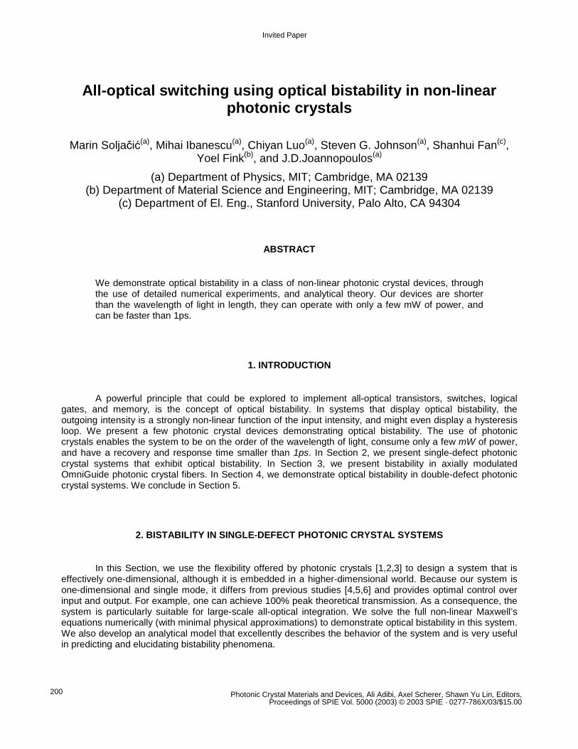
As a first numerical experiment, we launch off-resonance pulses whose envelope is Gaussian intime, with full-width at half-maximum (FWHM) ∆ω/ω0=1/1595, into the input waveguide. The carrier frequencyof the pulses is ω0=0.2573(2πc)/a so ωRES-ω0=3.8γ. When the peak power of the pulses is low, the total
output-pulse energy ( ∫∞
∞−≡ OUTOUT dtPE ) is only a small fraction (6.5%) of the incoming pulse energy EIN,
since we are operating off-resonance. As we increase the incoming pulse energy, the ratio EOUT/EIN
increases, at first slowly. However, as we approach the value of EIN=(0.57∗10-1)∗(λ0)2/cn2
(†), the ratioEOUT/EIN grows rapidly to 0.36; after this point, EOUT/EIN slowly decreases as we increase EIN. Thedependence of EOUT/EIN vs EIN is shown in Figure 2.
Figure 2: Transmission of Gaussian-envelope pulses through the device of Figure 1. As EIN isincreased, the EOUT/EIN ratio slowly grows. At a large enough EIN, the ratio of the outgoing and incomingpulse energies increases sharply.
Intuitively, as one increases the optical power, the increasing index due to the non-linearity lowersωRES through ω0, causing a rise and fall in transmission. This simple picture however is modified by non-linear feedback: as one moves into the resonance, coupling to the cavity is enhanced (positive feedback)creating a sharper on-transition and as one moves out of the resonance, the coupling is reduced (negativefeedback) causing a more gradual off-transition.
Consider now a repetition of the above simulation, but with continuous-wave (CW) signals launchedinto the cavity instead of Gaussian pulses. There are two reasons for doing this. First, the upper branch ofthe expected hysteresis curve is difficult to probe using only a single input pulse. Second, it is much simplerto construct an analytical theory explaining the phenomena when CW signals are used. In all cases, we findthat the amplitudes of the input signals grow slowly (compared with the cavity decay time) from zero to somefinal CW steady state values. Denoting by PIN
S, POUT
S the steady-state values of PIN and POUT respectively,we obtain the results shown by circles in Figure 3. For low PIN
S, POUTS slowly increases with increasing PIN
S.However, at a certain PIN
S, POUTS jumps discontinuously. This is precisely the desired performance, but it is
not the full story.
Hysteresis loops occur quite commonly in systems that exhibit optical bistability; an upper hysteresisbranch is the physical manifestation of the fact that the system “remembers” that it had a high POUT/PIN valueprevious to getting to the current value. To observe the upper hysteresis branch, we launch pulses that aresuperpositions of CW signals and Gaussian pulses (where the peak of the Gaussian pulse is significantlyhigher than the CW steady state value). In this way the Gaussian pulse will “trigger” the device into a high
†) Here, λ0 is the carrier wavelength in vacuum.
202 Proc. of SPIE Vol. 5000
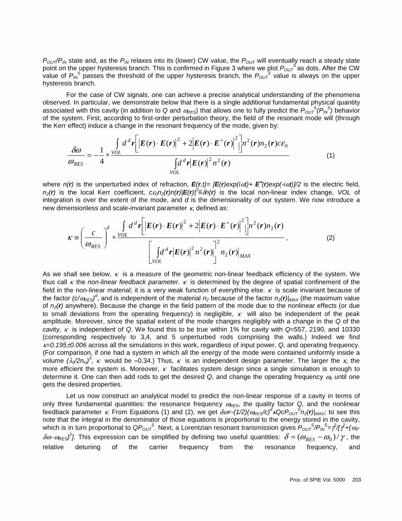
POUT/PIN state and, as the PIN relaxes into its (lower) CW value, the POUT will eventually reach a steady statepoint on the upper hysteresis branch. This is confirmed in Figure 3 where we plot POUT
S as dots. After the CWvalue of PIN
S passes the threshold of the upper hysteresis branch, the POUTS value is always on the upper
hysteresis branch.
For the case of CW signals, one can achieve a precise analytical understanding of the phenomenaobserved. In particular, we demonstrate below that there is a single additional fundamental physical quantityassociated with this cavity (in addition to Q and ωRES) that allows one to fully predict the POUT
S(PINS) behavior
of the system. First, according to first-order perturbation theory, the field of the resonant mode will (throughthe Kerr effect) induce a change in the resonant frequency of the mode, given by:
∫
∫
⋅+⋅
∗−=
∗
VOL
d
VOL
d
RES nd
cnnd
)()(
)()()()(2)()(
4
122
02222
rrEr
rrrErErErEr ε
ωδω
(1)
where n(r) is the unperturbed index of refraction, E(r,t)= [E(r)exp(iωt)+ E∗∗∗∗(r)exp(-iωt)]/2 is the electric field,n2(r) is the local Kerr coefficient, cε0n2(r)n(r)|E(r)|2≡δn(r) is the local non-linear index change, VOL ofintegration is over the extent of the mode, and d is the dimensionality of our system. We now introduce anew dimensionless and scale-invariant parameter κ, defined as:
MAXVOL
d
VOL
dd
RESnnd
nndc
)()()(
)()()()(2)()(
2
2
22
2222
rrrEr
rrrErErErEr
⋅+⋅
∗
≡
∫
∫ ∗
ωκ , (2)
As we shall see below, κ is a measure of the geometric non-linear feedback efficiency of the system. Wethus call κ the non-linear feedback parameter. κ is determined by the degree of spatial confinement of thefield in the non-linear material; it is a very weak function of everything else. κ is scale invariant because ofthe factor (c/ωRES)d, and is independent of the material n2 because of the factor n2(r)|MAX (the maximum valueof n2(r) anywhere). Because the change in the field pattern of the mode due to the nonlinear effects (or dueto small deviations from the operating frequency) is negligible, κ will also be independent of the peakamplitude. Moreover, since the spatial extent of the mode changes negligibly with a change in the Q of thecavity, κ is independent of Q. We found this to be true within 1% for cavity with Q=557, 2190, and 10330(corresponding respectively to 3,4, and 5 unperturbed rods comprising the walls.) Indeed we findκ=0.195±0.006 across all the simulations in this work, regardless of input power, Q, and operating frequency.(For comparison, if one had a system in which all the energy of the mode were contained uniformly inside avolume (λ0/2nH)3, κ would be ≈0.34.) Thus, κ is an independent design parameter. The larger the κ, themore efficient the system is. Moreover, κ facilitates system design since a single simulation is enough todetermine it. One can then add rods to get the desired Q, and change the operating frequency ω0 until onegets the desired properties.
Let us now construct an analytical model to predict the non-linear response of a cavity in terms ofonly three fundamental quantities: the resonance frequency ωRES, the quality factor Q, and the nonlinearfeedback parameter κ. From Equations (1) and (2), we get δω=-(1/2)(ωRES/c)dκQcPOUT
Sn2(r)|MAX; to see thisnote that the integral in the denominator of those equations is proportional to the energy stored in the cavity,which is in turn proportional to QPOUT
S. Next, a Lorentzian resonant transmission gives POUTS/PIN
S=γ2/[γ2+(ω0-δω−ωRES)2]. This expression can be simplified by defining two useful quantities: γωωδ /)( 0−= RES , the
relative detuning of the carrier frequency from the resonance frequency, and
Proc. of SPIE Vol. 5000 203
( ) ( )MAX
dRES ncQ
Pr2
1201
−≡ωκ
, a “characteristic power” of the cavity. With these definitions the relation
between POUTS and PIN
S becomes:
2
01
1
−+
=
δPPP
P
SOUT
SIN
SOUT . (3)
Thus, POUTS(PIN
S) is now reduced to depend on only two parameters, P0 and δ, each one of them havingseparate effects: a change in P0 is equivalent to a rescaling of both axes by the same factor, while the shapeof the curve can only be modified by changing δ. In general, cubic equation (3) can have either one or threereal solutions for POUT
S, depending on the value of the detuning parameter δ. The bistable regime
corresponds to three real solutions and requires a detuning parameter 3>δ . As mentioned earlier thedetuning in our simulations is ωRES−ω0=3.8γ, which means that δ = 3.8, well within the predicted bistabilityregime. Equation (3) is plotted in Figure 3 as a line for the case of Q=557 and κ=0.195. It is in excellentagreement with the results from the computational experiments, predicting both the upper and lowerhysteresis branches exactly. Note that the middle branch (dashed green line) is unstable in that tinyperturbations cause the solution to decay to either the upper, or lower branch [10].
1 2 3 4 5 60
PIN ( s
0
0.6
1.2
1.5
PO
UT (
s
x 10-5
x 10-5
T=100%P
OU
T ( P
)s
0
1
2
3
4
5
6
PIN (P)s
0
5 10 15 20
0.9
0.3
25
7
Figure 3: Plot of POUTS vs. PIN
S for the device of Figure 1. The circles are obtained by launching CWsignals into the device. The dots correspond to launching superpositions of Gaussian pulses and CWsignals into the cavity in order to access the hysteresis portion of the curve. The line is the analyticalprediction, corresponding to δ=3.8 and P0=2.6∗10-6λ0/n2.
From Eq. (3) one can also calculate some typical power levels for the device. For example, the inputpower needed for 100% transmission can be seen to be 0%100 PP δ= (corresponding to PIN
S=3.8P0 in Figure
3.) The minimum power needed for bistability is attained when 3=δ in which case we obtain
( ) ( )MAX
dRES
bncQ
PPr2
120min,3
3 −==ωκ
.
204 Proc. of SPIE Vol. 5000
Since the profiles of our modes are so similar to the cross-sections of the 3D modes described in Ref7, we can use our 2D simulations to estimate the power needed to operate a true 3D device. According towhat is shown in Ref 7, we are safe to assume that in a 3D device, the profile of the mode at differentpositions in the 3rd dimension will be roughly the same as the profile of the mode in the transverse directionof the 2D system. Thus, taking the Kerr coefficient to be n2=1.5*10-17m2/W, (a value achievable in manynearly-instantaneous non-linear materials), and a carrier wavelength λ0=1.55µm, gives a characteristic powerof P0=77mW, and a minimum power to observe bistability of Pb,min=133mW.
This level of power is many orders of magnitude lower than that required by other small all-opticalultra-fast switches! There are two reasons for this. First, the transverse area of the modes in the photoniccrystal in question is only ≈(λ/5)2; consequently, to achieve the same-size non-linear effects (which dependon intensity), we need much less power than in other systems that have larger transverse modal area.Second, since we are dealing with a highly confined, high-Q cavity, the field inside the cavity is much largerthan the field outside the cavity; this happens because of energy accumulation in the cavity. In fact, from theexpression for the characteristic power P0, one can see that the operating power falls as 1/Q2. Building ahigh-Q cavity that is also highly confined is very difficult in systems other than photonic crystals, so weexpect high-Q cavities in photonic crystals to be nearly optimal systems with respect to the power requiredfor optical bistability. For example, a Q=4000 would be quite useful for telecommunications, and leads to theoperational power of roughly 2.6mW. Moreover, the peak δn/n needed to operate the device would be 0.001,which is definitely possible with conventional instantaneous Kerr materials. Consequently, the response andrecovery time could easily be smaller than 1ps. Potential applications for such a device include: opticallogical gates, switches, optical regeneration, all-optical memory, and amplification [10].
3. OPTICAL BISTABILITY IN AXIALLY MODULATED OMNIGUIDE FIBERS
OmniGuide fibers are a new type of cylindrical multi-layer dielectric fibers [11] that have only veryrecently been implemented experimentally [12]. Their cladding is an omni-directional multi-layer mirror thatreflects light of any polarization and any direction. These photonic bandgap fibers can have a hollow coreand a guiding mechanism that depends only on the cladding. We propose to exploit these facts to obtainmuch stronger axial optical modulation than is possible in conventional fibers through insertion of material(e.g. spheres) into the core. Moreover, due to strong transverse confinement, much smaller transversemodal areas are possible than in usual low index-contrast fibers. In this way, we show how optimal ultra-fastbistable devices can be achieved with operating powers less than 40mW, whose highly nonlinearinput/output power relation is key to many applications [10] (e.g. all-optical pulse reshaping, optical limiting,logic gates, etc.). Our device retains all the advantages of similar photonic crystal (c.f. Section 2) or highindex-contrast devices [13] in terms of power, size, and speed. On the other hand, the fact that it is an in-fiber device should make it easier to produce and to couple with another fiber. We solve the full non-linearMaxwell’s equations numerically to demonstrate optical bistability in this class of systems. Moreover, wepresent an analytical model that excellently describes their behavior and is very useful in predicting optimaldesigns.
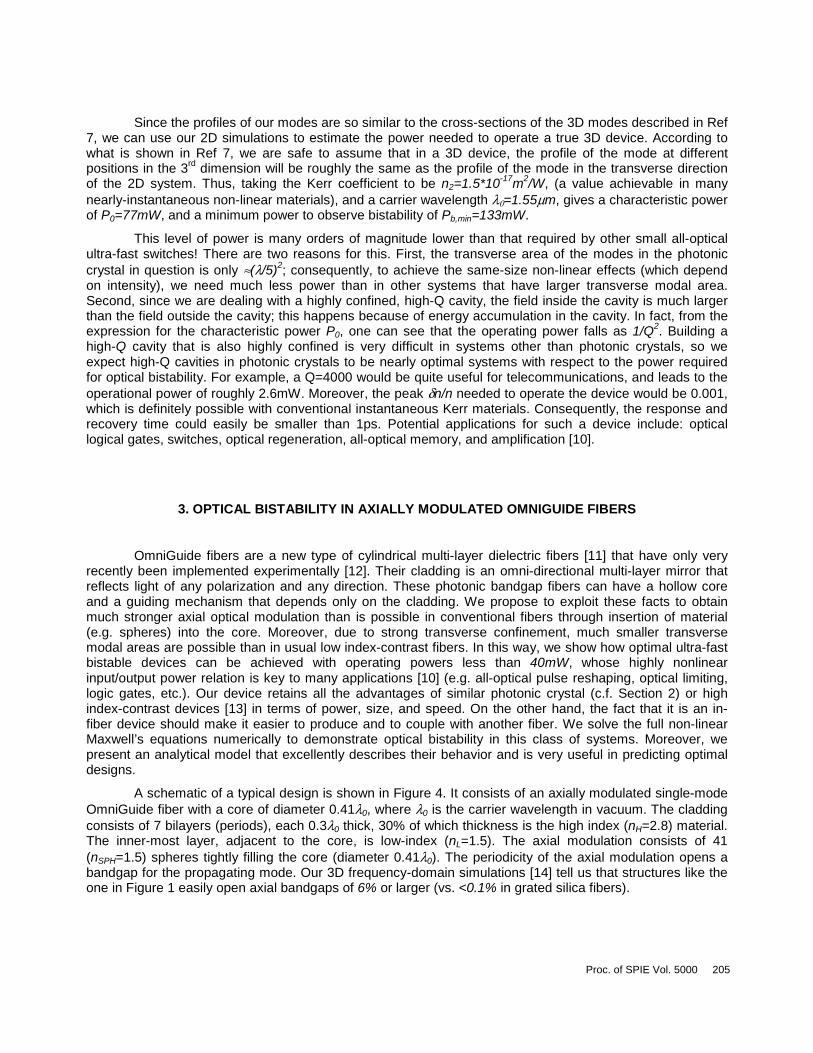
A schematic of a typical design is shown in Figure 4. It consists of an axially modulated single-modeOmniGuide fiber with a core of diameter 0.41λ0, where λ0 is the carrier wavelength in vacuum. The claddingconsists of 7 bilayers (periods), each 0.3λ0 thick, 30% of which thickness is the high index (nH=2.8) material.The inner-most layer, adjacent to the core, is low-index (nL=1.5). The axial modulation consists of 41(nSPH=1.5) spheres tightly filling the core (diameter 0.41λ0). The periodicity of the axial modulation opens abandgap for the propagating mode. Our 3D frequency-domain simulations [14] tell us that structures like theone in Figure 1 easily open axial bandgaps of 6% or larger (vs. <0.1% in grated silica fibers).
Proc. of SPIE Vol. 5000 205
Figure 4: Schematic of a non-linear OmniGuide device in which we demonstrate optical bistability. Theleft panel presents a longitudinal cross-section; the panel on the right presents a transverse cross-section.
A defect in the axial periodicity creates a resonant cavity supporting a tightly confined, high-Qresonant mode. In the implementation of Figure 4, the defect is introduced by changing the index ofrefraction of the central sphere to nDEF=1.9. Tight confinement in the transverse direction is provided by thelarge band-gap of the OmniGuide cladding, while strong confinement in the axial direction is provided by thelarge axial bandgap. The cavity couples to the waveguide (axially uniform fiber) through tunneling processes.We model the low-index material to have an instantaneous Kerr non-linearity (the index change isδn(r,t)=cnLε0n2|E(r,t)|2, where n2 is the Kerr coefficient.)
We perform nonlinear finite-difference time-domain (FDTD) simulations [8], with perfectly matchedlayers (PML) boundary condition, of this system. Due to the cylindrical symmetry of the system in Figure 4,our system is effectively two-dimensional. Consequently, we can obtain excellent physical understanding ofthe system by performing 2D FDTD simulations. The numerical values obtained with 2D calculations willdiffer from the true 3D values only by a geometrical factor of order unity.
The cavity supports a strongly localized resonant mode (transverse modal area ≈ λ2/3 and axiallength of the mode ≈ 6λ0). The system has a nearly Lorentzian transmission spectrum: T(ω)≡POUT(ω)/PIN(ω) ≈γW
2/[(γRγW2+(ω -ωRES)2], where POUT and PIN are the outgoing and incoming powers respectively, ωRES is the
resonant frequency, γW is the decay width due to the coupling of the cavity mode to the waveguides, while γR
is the decay width due to the coupling to the cladding modes [15]. We measure a quality factor Q=ωRES/[2(γR+γW]=540, and a peak transmission TP=0.88; from this we obtain that the radiation quality factorQR = ωRES/2γR = 8700. QR is finite due to the coupling of energy to the radiating cladding modes; this couplingis the primary cause of losses in our system, but can be controlled [16].
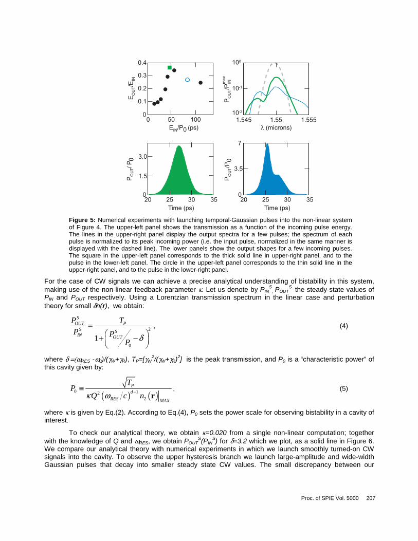
First, we perform numerical experiments in which we launch a series of Gaussian pulses into thesystem. We choose a carrier frequency ω0 = ωRES – 3.2(γWγR), and the full-width half-maximum (FWHM)bandwidth of our pulses is ω0/FWHM = 796. The ratio of the transmitted (EOUT) vs. incoming (EIN) pulseenergy increases sharply as we approach the bistability threshold, and decreases after the threshold ispassed, as shown in the upper-left panel of Figure 5. Transmitted pulse spectra are also shown for a fewpulses in upper-right panel of Figure 5; the non-linear cavity redistributes the energy in the frequencyspectrum; if these changes to the spectrum are undesirable, they can be removed by: optimizing the device,using time-integrating non-linearity, or by adding a frequency-dependent filter to the output of the device.Typical output-pulse shapes are shown in the lower panels of Figure 5. As one can see in the lower-leftpanel, even without optimizing our system, we still obtain well-behaved shapes of output pulses in the regimewhere EOUT/EIN is maximal.
206 Proc. of SPIE Vol. 5000
PO
UT/P
INmax
λ (microns)1.545 1.5551.55
10-1
10-2
100
PO
UT/P
0
20 25 30 350
3.5
7
Time (ps)
0
1.5
3.0
20 25 30 35Time (ps)
PO
UT/
P 0
0 50 1000
0.1
0.2
0.3
0.4
EO
UT/E
INEIN/P0
(ps)
Figure 5: Numerical experiments with launching temporal-Gaussian pulses into the non-linear systemof Figure 4. The upper-left panel shows the transmission as a function of the incoming pulse energy.The lines in the upper-right panel display the output spectra for a few pulses; the spectrum of eachpulse is normalized to its peak incoming power (i.e. the input pulse, normalized in the same manner isdisplayed with the dashed line). The lower panels show the output shapes for a few incoming pulses.The square in the upper-left panel corresponds to the thick solid line in upper-right panel, and to thepulse in the lower-left panel. The circle in the upper-left panel corresponds to the thin solid line in theupper-right panel, and to the pulse in the lower-right panel.
For the case of CW signals we can achieve a precise analytical understanding of bistability in this system,making use of the non-linear feedback parameter κ. Let us denote by PIN
S, POUT
S the steady-state values ofPIN and POUT respectively. Using a Lorentzian transmission spectrum in the linear case and perturbationtheory for small δn(r), we obtain:
2
01
SOUT P
S SIN OUT
P T
P PP δ
= + −
, (4)
where δ =(ωRES -ω0)/(γW+γR), TP=[γW2/(γW+γR)2] is the peak transmission, and P0 is a “characteristic power” of
this cavity given by:
( ) ( )0 122
Pd
RES MAX
TP
Q c nκ ω −≡r
, (5)
where κ is given by Eq.(2). According to Eq.(4), P0 sets the power scale for observing bistability in a cavity ofinterest.
To check our analytical theory, we obtain κ=0.020 from a single non-linear computation; togetherwith the knowledge of Q and ωRES, we obtain POUT
S(PINS) for δ=3.2 which we plot, as a solid line in Figure 6.
We compare our analytical theory with numerical experiments in which we launch smoothly turned-on CWsignals into the cavity. To observe the upper hysteresis branch we launch large-amplitude and wide-widthGaussian pulses that decay into smaller steady state CW values. The small discrepancy between our
Proc. of SPIE Vol. 5000 207
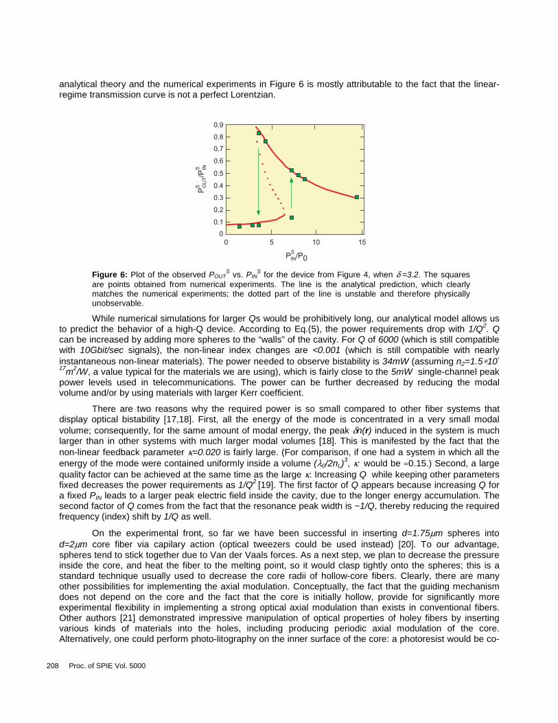
analytical theory and the numerical experiments in Figure 6 is mostly attributable to the fact that the linear-regime transmission curve is not a perfect Lorentzian.
0.9
PO
UT/P
INSS
0.8
0.7
0.6
0.5
0.4
0.3
0.2
0.1
0
PIN/P0S
0 5 10 15
Figure 6: Plot of the observed POUTS vs. PIN
S for the device from Figure 4, when δ =3.2. The squaresare points obtained from numerical experiments. The line is the analytical prediction, which clearlymatches the numerical experiments; the dotted part of the line is unstable and therefore physicallyunobservable.
While numerical simulations for larger Qs would be prohibitively long, our analytical model allows usto predict the behavior of a high-Q device. According to Eq.(5), the power requirements drop with 1/Q2. Qcan be increased by adding more spheres to the “walls” of the cavity. For Q of 6000 (which is still compatiblewith 10Gbit/sec signals), the non-linear index changes are <0.001 (which is still compatible with nearlyinstantaneous non-linear materials). The power needed to observe bistability is 34mW (assuming n2=1.5∗10-
17m2/W, a value typical for the materials we are using), which is fairly close to the 5mW single-channel peakpower levels used in telecommunications. The power can be further decreased by reducing the modalvolume and/or by using materials with larger Kerr coefficient.
There are two reasons why the required power is so small compared to other fiber systems thatdisplay optical bistability [17,18]. First, all the energy of the mode is concentrated in a very small modalvolume; consequently, for the same amount of modal energy, the peak δn(r) induced in the system is muchlarger than in other systems with much larger modal volumes [18]. This is manifested by the fact that thenon-linear feedback parameter κ=0.020 is fairly large. (For comparison, if one had a system in which all theenergy of the mode were contained uniformly inside a volume (λ0/2nL)
3, κ would be ≈0.15.) Second, a largequality factor can be achieved at the same time as the large κ. Increasing Q while keeping other parametersfixed decreases the power requirements as 1/Q2 [19]. The first factor of Q appears because increasing Q fora fixed PIN leads to a larger peak electric field inside the cavity, due to the longer energy accumulation. Thesecond factor of Q comes from the fact that the resonance peak width is ~1/Q, thereby reducing the requiredfrequency (index) shift by 1/Q as well.
On the experimental front, so far we have been successful in inserting d=1.75µm spheres intod=2µm core fiber via capilary action (optical tweezers could be used instead) [20]. To our advantage,spheres tend to stick together due to Van der Vaals forces. As a next step, we plan to decrease the pressureinside the core, and heat the fiber to the melting point, so it would clasp tightly onto the spheres; this is astandard technique usually used to decrease the core radii of hollow-core fibers. Clearly, there are manyother possibilities for implementing the axial modulation. Conceptually, the fact that the guiding mechanismdoes not depend on the core and the fact that the core is initially hollow, provide for significantly moreexperimental flexibility in implementing a strong optical axial modulation than exists in conventional fibers.Other authors [21] demonstrated impressive manipulation of optical properties of holey fibers by insertingvarious kinds of materials into the holes, including producing periodic axial modulation of the core.Alternatively, one could perform photo-litography on the inner surface of the core: a photoresist would be co-
208 Proc. of SPIE Vol. 5000
drawn as the inner-most layer of the cladding, laser beams shone from the side would implement cross-linking of the photo-resist, and then the hollow core would be used to transport all the acids and/or basesneeded to etch a periodic structure onto the inner-most layer of the cladding.
We would like to emphasize that since the transverse confinement principle is not index guiding,periodic axial modulation is not the only way to achieve axial confinement in OmniGuide fibers. In fact, simplyshrinking the core radius [21] (or equivalently decreasing the index of the core) of an OmniGuide fiber canshift the cutoff frequency of the operating mode above the operating frequencysimilarly to a metallicwaveguide, a mode experiences an exponential decay once it encounters such a region; this property issufficient to implement all the ideas presented above. Finally, one should be able to implement all theprinciples described in this manuscript in any hollow photonic crystal fiber that has a large enough lateralbandgap.
4. BISTABILITY IN DOUBLE-DEFECT PHOTONIC CRYSTAL SYSTEMS
In this Section, we describe a novel device system with 4 ports that provides very important newperformance characteristics. For example, essentially no portion of the incoming pulse is ever reflected backinto the input waveguide. Having zero reflection is of crucial importance for integration with other activedevices on the same chip. Through the use of analytical theory, and detailed numerical simulations, weexplain this device’s underlying physics and demonstrate its operation as an all-optical transistor and foroptical isolation.
Ideally, for many applications one would like to have a device with two inputs whose output has astrong dependence on the (weak) amplitude of one of its inputs (the probe input). Moreover, for ultimateefficiency, one would require single-mode waveguiding, high-Q cavities, and controllable radiation losses. Anon-linear PC system can provide us with all of these capabilities.
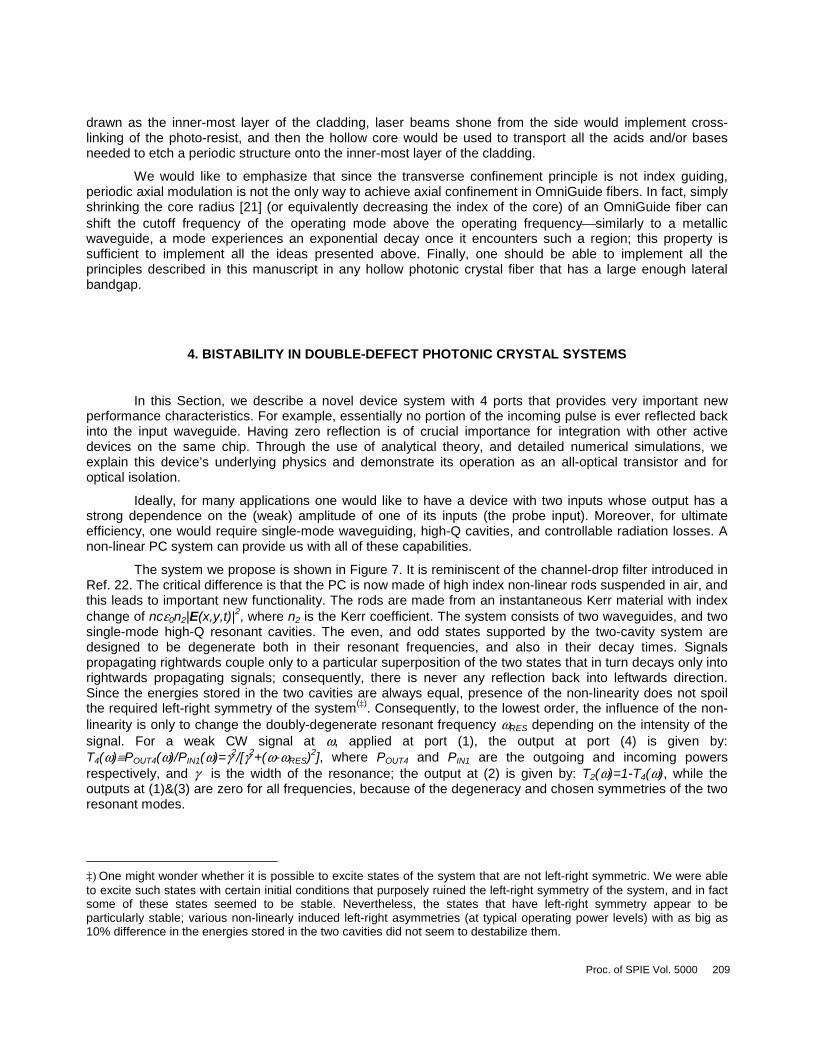
The system we propose is shown in Figure 7. It is reminiscent of the channel-drop filter introduced inRef. 22. The critical difference is that the PC is now made of high index non-linear rods suspended in air, andthis leads to important new functionality. The rods are made from an instantaneous Kerr material with indexchange of ncε0n2|E(x,y,t)|2, where n2 is the Kerr coefficient. The system consists of two waveguides, and twosingle-mode high-Q resonant cavities. The even, and odd states supported by the two-cavity system aredesigned to be degenerate both in their resonant frequencies, and also in their decay times. Signalspropagating rightwards couple only to a particular superposition of the two states that in turn decays only intorightwards propagating signals; consequently, there is never any reflection back into leftwards direction.Since the energies stored in the two cavities are always equal, presence of the non-linearity does not spoilthe required left-right symmetry of the system(‡). Consequently, to the lowest order, the influence of the non-linearity is only to change the doubly-degenerate resonant frequency ωRES depending on the intensity of thesignal. For a weak CW signal at ω, applied at port (1), the output at port (4) is given by:T4(ω)≡POUT4(ω)/PIN1(ω)=γ2/[γ2+(ω-ωRES)2], where POUT4 and PIN1 are the outgoing and incoming powersrespectively, and γ is the width of the resonance; the output at (2) is given by: T2(ω)=1-T4(ω), while theoutputs at (1)&(3) are zero for all frequencies, because of the degeneracy and chosen symmetries of the tworesonant modes.
‡) One might wonder whether it is possible to excite states of the system that are not left-right symmetric. We were ableto excite such states with certain initial conditions that purposely ruined the left-right symmetry of the system, and in factsome of these states seemed to be stable. Nevertheless, the states that have left-right symmetry appear to beparticularly stable; various non-linearly induced left-right asymmetries (at typical operating power levels) with as big as10% difference in the energies stored in the two cavities did not seem to destabilize them.
Proc. of SPIE Vol. 5000 209
port 1
port 3
port 2
port 4
port 1
port 3
port 2
port 4
Figure 7: Basic 4-port non-linear PC device that we use to demonstrate optical bistability. The PCconsists of high-index εH=11.56 rods with radius 0.2a, a being the lattice constant. The four differentlycolored rods in each plot have ε=9.5; the small rods have ε=6.2, and radius of 0.05a. As an example ofthe use of the device, we show the electrical fields in the case when it performs optical isolation. Topshows a strong forward-propagating pulse. Bottom shows a weak reflected backward-propagatingpulse. We model the high index rods as having an instantaneous Kerr non-linearity.
Given these forms for the transmission, we can follow the framework of Section 2 to predict that thesystem will exhibit optical bistability if the carrier frequency ω0 is sufficiently below the resonant frequency:
( ) 30 >−≡ γωωδ RES . Using the analytical framework of Section 2, the steady state values of the CW
powers of interest are:2
0
41
4
1
1
−+
=
δPPP
P
SOUT
SIN
SOUT , and POUT2
S/PIN1S=1-POUT4
S/PIN1S, where
“characteristic power”,( ) ( )
MAXRES ncQP
r220
1
ωκ≡ . We establish that for the current system the non-
linear feedback parameter κ=0.11, while the quality factor is Q=ωRES/2γ=730. For definiteness, we takeδ=4.25, so bistability should be easily observable. We plot the analytical prediction as the green line in Figure8; the dashed portion of that line is unstable, and thereby physically unobservable.
To verify this simple and powerful prediction, we perform numerical experiments (non-linear finite-difference time-domain (FDTD) simulations with perfectly matched layers (PML) boundary conditions) on thissystem. The current work, and the work of Ref. 22, are for a 2D model; this decreases numericalrequirements on our simulations significantly compared to 3D simulations. Nevertheless, it has been shown
210 Proc. of SPIE Vol. 5000

recently [7] that one can find an equivalent 3D system that will behave qualitatively the same, while thequantitative differences will be only of a geometrical factor close to 1.
2 4 6 8 10 12 14 160
0.5
1.0
PO
UT
2 /
PIN
1 s
s
PIN1 (P)s0
2 4 6 8 10 12 14 160
0.5
1.0
PO
UT
4 /
PIN
1 s
s
Figure 8: Plots of the observed T≡POUTS/PIN
S vs. PINS for the device from Figure 7. The upper panel
shows the power observed at output (2), while the lower panel shows the power observed at output (4).The input signal enters the device at port (1). The circles are points obtained by launching CW signalsinto our device. The dots are measurements that one observes when launching superpositions ofGaussian pulses and CW signals into the system. The lines are from an analytical model described inthe text.
To observe the lower bistability hysteresis branch, we send smooth CW signals into the port (1) ofthe system, and we vary the peak power of the incoming signals. In order to observe the upper bistabilityhysteresis branch, we launch superpositions of wide Gaussian pulses that decay into smaller-intensity CWsignals, thereby relaxing into the points on the upper hysteresis branch. As shown in Figure 8, this deviceindeed displays optical bistability, and our analytical model is a very good representation of the physicalreality. Throughout all of these simulations, the observed reflections back into ports (1)&(3) are always lessthan 1% of the incoming signal’s power.
Given that the modes of the 2D system are so similar to the cross-sections of the modes describedin Ref.7, we can use the 2D results, together with the analytical model of the system to predict theperformance of the device in a real physical setting. According to Ref.7, once this device is implemented in aPC with complete 3D bandgap, the 3rd dimension extent of all the modes will be roughly λ/3. Let us assumethat the Kerr coefficient of the material we are using is n2=1.5*10-17m2/W, (a value achievable in many nearly-instantaneous non-linear materials, e.g. GaAs). Assuming a device with Q=4000 (which is still compatiblewith 10Gbit/s signals), and carrier wavelength λ0=1.55µm, we get that the characteristic power of the deviceis P0≈5mW, while the peak operating power needed to observe bistability is roughly 8mW. (Compare this tothe 5mW peak power levels used in telecommunications today). The peak non-linearly induced δn/n<0.001,which is compatible with using nearly-instantaneous non-linear materials.
Proc. of SPIE Vol. 5000 211
Let us now examine how we would use such a device for optical isolation. One of the biggestobstacles in achieving large-scale optics integration today is the non-existence of integrated optical isolators;active and non-linear devices typically do not tolerate small reflections coming from other devices they areintegrated with. The most common approach involves breaking the time-reversal symmetry using magneto-optic materials; other approaches involve breaking backward-forward symmetry using non-linear materials[23]. Unfortunately, none of these approaches satisfy all the requirements mentioned earlier which arenecessary for large-scale optics integration. The device of Figure 7 can perform integrated-optics isolation,for most applications of interest, eg. where the strength of each logical (forward-propagating) signal in aparticular waveguide is above the bistability threshold, and the reflected (backward-propagating) signals areweak. An example of such operation is shown in Figure 7. A strong forward-propagating signal (operating ata high-transmission point of the bistability curve) is nearly perfectly transferred from port (1) to port (4).However, when a weak reflected signal (operating at a low-transmission point of the bistability curve) entersport (4) of the device at a later time, it proceeds to port (3), from where it can be discarded.
0 5000 100000
1
2
3
PO
UT
4 / P
INmax
PO
UT
4 (P
) 0
0
Time (2π/ω )0
2000 4000 0 0.05 0.1
0.368 0.369 0.3710.370
10-1
10-2
100
0.15
0.4
0.20
0.25
0.30
0.3
0.2
0.1
0
ωa/(2πc )
UO
UT
4 / U
IN1
UO
UT
4 / U
IN1
UIN1 (2πP/ω )00 sqrt (UIN3 / UIN1)
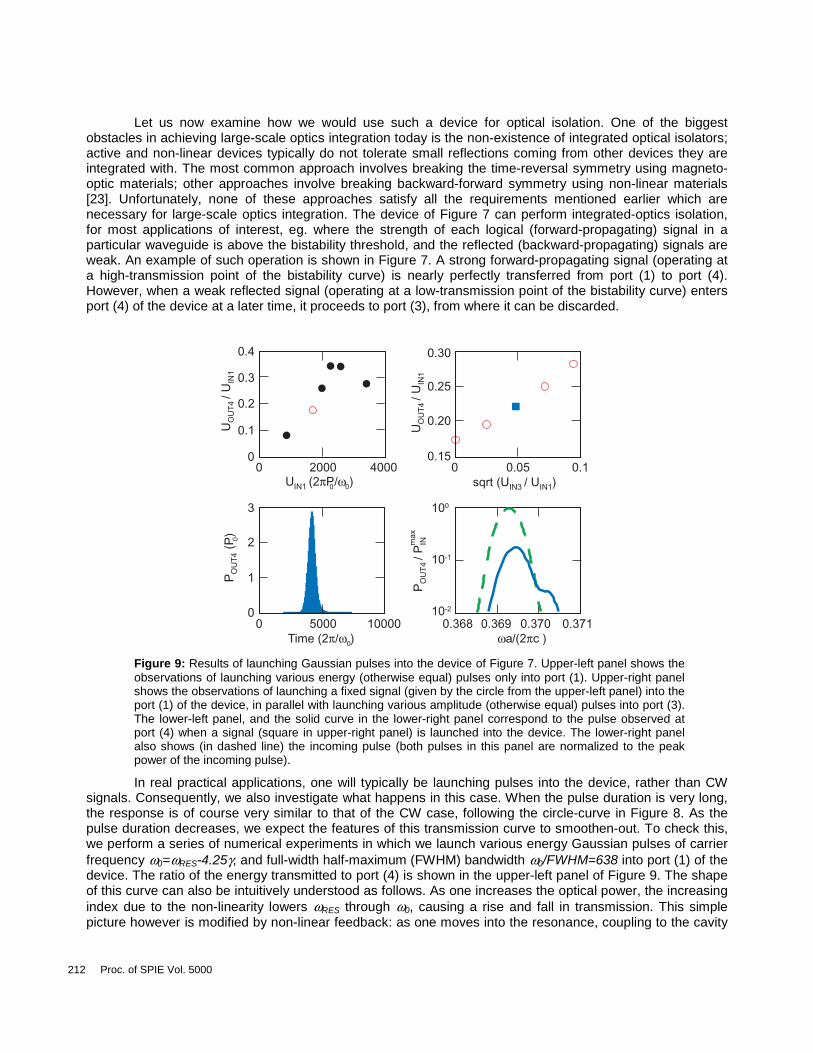
Figure 9: Results of launching Gaussian pulses into the device of Figure 7. Upper-left panel shows theobservations of launching various energy (otherwise equal) pulses only into port (1). Upper-right panelshows the observations of launching a fixed signal (given by the circle from the upper-left panel) into theport (1) of the device, in parallel with launching various amplitude (otherwise equal) pulses into port (3).The lower-left panel, and the solid curve in the lower-right panel correspond to the pulse observed atport (4) when a signal (square in upper-right panel) is launched into the device. The lower-right panelalso shows (in dashed line) the incoming pulse (both pulses in this panel are normalized to the peakpower of the incoming pulse).
In real practical applications, one will typically be launching pulses into the device, rather than CWsignals. Consequently, we also investigate what happens in this case. When the pulse duration is very long,the response is of course very similar to that of the CW case, following the circle-curve in Figure 8. As thepulse duration decreases, we expect the features of this transmission curve to smoothen-out. To check this,we perform a series of numerical experiments in which we launch various energy Gaussian pulses of carrierfrequency ω0=ωRES-4.25γ, and full-width half-maximum (FWHM) bandwidth ω0/FWHM=638 into port (1) of thedevice. The ratio of the energy transmitted to port (4) is shown in the upper-left panel of Figure 9. The shapeof this curve can also be intuitively understood as follows. As one increases the optical power, the increasingindex due to the non-linearity lowers ωRES through ω0, causing a rise and fall in transmission. This simplepicture however is modified by non-linear feedback: as one moves into the resonance, coupling to the cavity
212 Proc. of SPIE Vol. 5000

is enhanced (positive feedback) creating a sharper on-transition and as one moves out of the resonance, thecoupling is reduced (negative feedback) causing a more gradual off-transition.
As an illustration of another possible application of our device, we now exploit this sharper on-transition to construct an all-optical transistor. We perform a series of numerical experiments in which welaunch into port (1) the pulses presented by the circle in the upper-left panel of Figure 9; however, in additionto this, we send identical (albeit smaller energy) pulses into port (3) of the system. We experimented withlaunching a few different energy pulses into (3); the results are shown in the upper-right panel of Figure 9. Aswe can see, the amplification can be quite drastic. Consider for example the square in that panel: the pulsesent into (3) had 0.25% of the energy of the pulse sent thru (1), resulting in an almost 5% increase intransmission to port (4); this implies an amplification of a factor of roughly 20. Such large amplifications areprecisely the functionality one expects from an all-optical transistor (c.f. Section 2). An additional interestingfeature of the upper-right panel of Figure 9, is that the energy observed at port (4) is essentially proportionalto the square root of the energy sent in thru (3). This means that the energy amplification factor becomesinfinite as the signal energy goes to zero, which may have some exciting new applications, such as a verylow threshold laser. This behavior can be understood as follows. Pulses coming in thru (1)&(3) are coherentand in phase. Consequently, (taking into account the up-down symmetry of the system), once inside thecavities, the signals add in amplitude. Therefore, for small signals, and a given pulse incoming thru (1), theenergy stored in the cavity is a linear function of the field applied at (3). Since the energy at (4) is a linearfunction of the energy stored in the cavities, it is a linear function of the square root of the energy coming thru(3). If instead we considered a time-integrating non-linearity, and temporally incoherent signals, for a fixedincoming pulse at (1), the energy output at (4) would be a linear function of the energy coming into (3) (in thatcase, the signals in the cavity would add in intensity, rather than in amplitude). Finally, since the frequencywidth of the pulses is comparable to the frequency width of the cavity, and the non-linear effects are quiteextreme, it is important to determine possible distortions in the shapes of the output pulses. The use of FDTDsimulations provides a bonus here, since a detailed description of output pulses is typically not feasible withother theoretical models. In general, we find that the output pulses retain their pulse shape, as shown in thelower panels of Figure 9.
With only minor modifications, the device system we propose can also be used for other applications[10], including: any all-optical logical gate, pulse reshaping and regeneration, noise-cleanup, optical diode[4], memory, etc. For any of these uses, when applying any signal to port (1) and/or port (3), one never hasto worry about any reflections into ports (1) or (3). The control of reflections offered by devices of this typerepresents a low-power, ultra-fast, small-scale paradigm for implementing non-linear micro-devices in non-linear optics.
5. CONCLUSION
We demonstrated how unique opportunities of photonic crystals for molding the flow of light openeda new window of opportunity for using optical bistability for all-optical applications. Devices that can bedesigned using these principles are suitable for implementing large-scale optics integration, they are tiny insize, can be ultra-fast and operate with only a few mW of power.
We are especially grateful to Steve Jacobs, Torkel Engeness, Ori Weisberg and MaksimSkorobogatiy from OmniGuide Communications, Inc., for their help in developing the non-linear finitedifference time domain code used in these simulations. We would also like to thank Prof. Moti Segev fromTechnion, and Prof. Erich Ippen of MIT for many useful discussions. This work was supported in part by theMaterials Research Science and Engineering Center program of the National Science Foundation underGrant No. DMR-9400334.
Proc. of SPIE Vol. 5000 213

REFERENCES
1 E. Yablonovitch, Phys. Rev. Lett. 58, 2059 (1987).
2 S. John, Phys. Rev. Lett. 58, 2486 (1987).
3 J. D. Joannopoulos, R. D. Meade, and J. N. Winn, Photonic Crystals: Molding the flow of light (PrincetonUniversity Press, Princeton, N.J., 1995).
4 S. F. Mingaleev, and Y. S. Kivshar, J. Opt. Soc. Am. B 19, 2241 (2002).
5 E. Centeno, and D. Felbacq, Phys. Rev. B, 62, R7683 (2000).
6 B. Xu, and N. Ming, Phys. Rev. Lett. 71, 3959 (1993).
7 M. L. Povinelli, S. G. Johnson, S. Fan, and J. D. Joannopoulos, Phys. Rev. B 64, 075313 (2001).
8 For a review, see A. Taflove, Computational Electrodynamics: The Finite-Difference Time-Domain Method(Artech House, Norwood, Mass., 1995).
9 A. Mekis, S. Fan, and J. D. Joannopoulos IEEE Microwave Guided Wave Lett. 9, 502 (1999).
10 B. E. A. Saleh, and M. C. Teich, Fundamentals Of Photonics (John Wiley&Sons, 1991).
11 Y. Fink, D. J. Ripin, S. Fan, C. Chen, J. D. Joannopoulos, and E. L. Thomas, J. Lightwave Tech. 17, 2039(1999); Steven G. Johnson, Mihai Ibanescu, M. Skorobogatiy, Ori Weisberg, Torkel D. Engeness, MarinSoljačić, Steven A. Jacobs, J. D. Joannopoulos, and Yoel Fink, Optics Express, 9, 748, (2001).
12 S.D.Hart, G.R.Maskaly, B.Temelkuran, P.H.Prideaux, J.D.Joannopoulos, Y.Fink, Science 296, 511-513 (2002).
13 J.S.Foresi, P.R.Villeneuve, J.Ferrera, E.R.Thoen, G.Steinmeyer, S.Fan, J.D.Joannopoulos, L.C.Kimerling,H.I.Smith, and E.P.Ippen, Nature, 390, 143, (1997).
14 Steven G. Johnson and J. D. Joannopoulos, Optics Express 8, no. 3, 173-190 (2001).
15 See e.g. Shanhui Fan, Pierre R. Villeneuve, J.D.Joannopoulos, and H.A.Haus, Physical Review B, 64, 245302,(2001), and H.A.Haus, Waves And Fields in Optoelectronics (Prentice-Hall, Englewood Cliffs, NJ, 1984).
16 S.G.Johnson, S.Fan, A.Mekis, and J.D.Joannopoulos, Applied Physics Letters, 78, 3388 (2001).
17 S.Coen and M.Haelterman, Optics Letters, 24, 80 (1999).
18 Stojan Radić, Nicholas George, and Govind P. Agrawal, JOSA B, 12, 671 (1995).
19 A.Yariv, IEEE Photonics Technology Letters, 14, 483, (2002), and J.E.Heebner, and R.Boyd, Optics Letters, 24,847 (1999).
20 Burak Temelkuran, personal communication.
21 C.Kerbage, and B.J.Eggleton, Optics&Photonics News, 38, September 2002.
22 S.Fan, P.R.Villeneuve, J.D.Joannopoulos, and H.A.Haus, Phys. Rev. Lett. 80, 960 (1998).
23 M.Scalora, J.P.Dowling, M.J.Bloemer, and C.M.Bowden, Journal of Applied Physics 76, 2023 (1994); K. Gallo,G. Assanto, K. R. Parameswaran, and M. M. Fejer, Appl. Phys. Lett. 79, 314 (2001)
214 Proc. of SPIE Vol. 5000


![· 2010. 3. 13. · optical bistability (0B), optica) fibrE9, optical corupubers xnd quautum puters {1-7]. In addition,](https://img.pdfslide.us/doc/110x75/6121df10d48a294b69389082/2010-3-13-optical-bistability-0b-optica-fibre9-optical-corupubers-xnd.jpg)