Embed Size (px)
Citation preview
189
CHAPTER 7
ALL-OPTICAL PLASMONIC MODULATORS AND
INTERCONNECTS
Domenico Pacifici, Henri J. Lezec, Luke A. Sweatlock, Chris de Ruiter, Vivian
Ferry, and Harry A. Atwater
Thomas J. Watson Laboratories of Applied Physics, California Institute of
Technology, 1200 E California Blvd., Pasadena, CA 91125, USA
We present experimental results and design guidelines for optical
modulators and interconnects based on metallo-dielectric plasmonic
structures. The short wavelengths and high field confinements of
surface plasmon polaritons at the metal/dielectric interfaces allow for
the manipulation and guidance of optical signals in very compact and
power-efficient devices, amenable to ultra-large scale integration of on-
chip optical functionalities.
1. Introduction
Relative to electrons, photons are characterized by lower heat
dissipation, better immunity to crosstalk, lower dispersion, and huge
information capacity due to their large bandwidths at optical frequencies.
Because of these attractive features, researchers have long pursued the
use of photons as the new information carriers, for demanding
computations and optical data processing,1,2
and as a long-term solution
to the interconnection bottleneck problem in microelectronics.3-5
Essential building blocks for all-optical computation and networks, such
as logic elements and modulators, have already been demonstrated.6-9
However, despite the encouraging premises, all-optical integrated
information processing has thus far remained elusive. Indeed, state-of-
the-art optical modulators and interconnects typically rely upon weak,
inefficient light-matter interactions, which call for large operating power
D. Pacifici et al. 190
densities10
and long interaction distances (millimeters to centimeters),11
thus limiting the opportunity for dense chip-based integration of all-
optical functionalities. Moreover, due to diffraction, the wavelength of
light typically sets a lower limit to further scaling down the feature size
and increasing device density in conventional dielectric waveguide
architectures.
Plasmonics, with its ability to confine and guide electromagnetic
waves in subwavelength metallo-dielectric structures,12,13
promises to be
a valuable alternative to the implementation of compact, fast and power-
efficient optical integrated networks.14-16
In this chapter we investigate
the use of subwavelength scatterers and corrugations in a metal as
efficient, localized sources of surface plasmon polaritons (SPPs)
propagating for several micrometers at the dielectric/metal interface.
Several authors have reported, both theoretically and experimentally, that
optical transmission through a subwavelength slit in metal films can be
strongly influenced by the presence of nearby surface features, such as
grooves or other slits.17-24
We precisely measure and then modulate the
propagation constants of the generated surface plasmon polaritons, using
a set of surface wave interferometers consisting of a pair of parallel
groove and slit, in which the distance between the slit and the groove is
systematically varied up to several micrometers.25
Light directly incident on the slit interferes with the propagating SPP,
which originates from the groove and reaches the slit location with a
phase shift determined by a characteristic scattering phase lag26,27
and a
propagative phase depending on travelled distance. By varying the length
of the interferometer arm, i.e. changing the distance between the slit and
the groove, we determine the dispersion relation and propagation length
of SPPs in a wide spectral range, i.e. from 400 to 1500 nm.
Active manipulation of the SPP is then achieved by coating the arm
of the interferometer with an active medium, consisting, for instance, of a
thin film of CdSe semiconductor quantum dots (QDs) fabricated by
colloidal chemical synthesis in solution.28
The QDs have been
specifically designed to show an absorption bandgap at ~600 nm,
therefore they can absorb high frequency surface plasmons (in the green-
blue spectral range) while being transparent to surface plasmons at
infrared wavelengths. Active modulation is achieved by means of two
All-Optical Plasmonic Modulators and Interconnects
191
co-propagating SPPs launched by the groove. A control (pump) SPP
having a free-space wavelength of 514.5 nm is absorbed in
photogeneration of electron-hole pairs inside the QD volume while
propagating along the metal-dielectric interface. A signal (probe) SPP at
1.5 µm copropagating with the control SPP is then absorbed by
promoting an intraband transition in the quantum dots, that is, by re-
exciting the electron to a higher energy level. As soon as the pump SPP
is turned off, the probe SPP is no longer absorbed, as the QDs quickly (in
less than 40 ns) return to their transparent ground state. The modulated
amplitude of the probe SPP determines a quick change in the interference
conditions at the slit, thus causing a change in the interferometer output
state (“on” and “off”). Thanks to the highly confined nature of the SPP
field and the large quantum-dot absorption cross-section, the fast all-
optical plasmonic modulation can be achieved at very-low power
densities, in micrometer-scale planar devices.25
We further design and fabricate a three-dimensional prototype of
plasmonic modulator, employing a Mach-Zehnder interferometer in a
multilevel metal-dielectric-metal stack, where the dielectric is made
active by the presence of QDs. By opportunely varying the arms of the
interferometers, higher modulation depths are achieved. Moreover, by
exploiting the polarization properties of subwavelength slits in a metal
film, we demonstrate optical isolation between the control and signal
SPPs using cross-polarized incident beams incoupled into SPPs by
perpendicularly-oriented slits. Finally, we present a design study for
three-dimensional plasmonic vias and modulators, and investigate
several schemes for coupling light into such devices, evaluating their
power efficiency.
2. Surface plasmon interferometers
2.1. Fabrication and experimental methods
We fabricated several on-chip planar interferometers consisting of a
single subwavelength aperture flanked by a subwavelength groove in a
metal film. Identical subwavelength structures were fabricated by

D. Pacifici et al. 192
focused ion beam (FIB) milling into a 400 nm thick layer of Ag
evaporated onto flat fused silica microscope slides. A low beam current
(50 pA) was used to achieve surface features defined with a lateral
precision of the order of 10 nm and characterized by near-vertical
sidewalls and a minimal amount of edge rounding. The milled groove
and slit were 10 µm long, 200 and 100 nm wide, and 100 nm and 400 nm
deep, respectively. The slit-groove separation distance was
systematically varied in the range 500-10400 nm, in step of 50 nm, with
a precision of 1%. A series of single apertures is also milled for reference
purposes. The same set of structures was milled in another silver film
(co-evaporated with the previous sample) which was previously spin-
coated with a thin film of densely-packed CdSe QDs obtained by
colloidal chemical synthesis in solution.28
The QDs were capped with
trioctylphosphine oxide (TOPO) ligands. Multiple spin-coatings of the
toluene solution containing CdSe QDs were performed at 1000 rpm for 1
minute, followed by a thermal treatment at 150°C for 5 minutes. A 24
nm-thick film of densely-packed CdSe QDs was formed, with a good
uniformity over the entire silver surface. The QDs showed bright
photoluminescence (PL) peaked at 625 nm.
Transmission measurements were performed on both QD-coated and
uncoated interferometers by focusing a laser beam onto the patterned
side (Ag-air side) of each sample. The film thickness is such that the
devices are optically opaque at the groove position, and light is only
transmitted through the slit aperture. This approach allows us to achieve
high signal-to-noise ratios in our experiments. The light intensity
transmitted through the slit of each interferometer was gathered by a 50X
microscope objective, sent to a single grating monochromator and
detected with a liquid-nitrogen-cooled CCD array detector (spectral
range: 400–900 nm), with an ultra-sensitive liquid-nitrogen-cooled
germanium detector (spectral range: 900–1700 nm), or with a fast
photomultiplier tube with an extended near-infrared spectral response
(range 300–1700 nm).
Colour plate 1(a) at the end of the chapter displays a schematic of a
typical interferometer consisting of a single slit of subwavelength width
etched completely through a metallic film on a transparent substrate
flanked by a single parallel groove, etched partially through the metal.

All-Optical Plasmonic Modulators and Interconnects
193
The center-to-center separation distance between slit and groove is
defined as D. The blue spheres represent CdSe QDs. Two beams (signal
and control) uniformly illuminate the structure. Diffractive scattering by
the groove excites SPPs at two different frequencies, which we call the
control and signal SPP, respectively. Colour plate 1(b) reports an SEM
micrograph of an uncoated interferometer, with visible groove and slit.
2.2. Theoretical framework
Let us consider a TM-polarized (H field parallel to the longer slit side)
electromagnetic plane wave with free space wavelength λ (and free space
wavevector � � 2�/�) impinging on the entire surface at an angle �
with respect to the sample normal. Diffractive scattering by the groove
couples a fraction � of the incident field amplitude into a surface wave
with amplitude that reaches the slit with an overall phase shift:
� � �� sin � � �� � �� � � �� 2⁄ , (1)
where the first term is the phase shift due to the free-space optical path
length difference between the incident wavefronts reaching the aperture
and the groove, the second term is the phase shift gained by the surface
wave traveling with surface wavevector � � �� � 2��/� (where � is the real part of the effective refractive index of the surface wave), and
the third term is the phase shift introduced by scattering at the groove.
The fourth imaginary term in Eq. (1) accounts for absorption or
scattering loss experienced by the surface wave propagating along the
surface (where � � 4��/� is the overall absorption coefficient, � being
the imaginary part of the effective refractive index of the surface wave).
At the slit entrance, both the directly incident light and the SPP arriving
from the groove are coupled into guided slit modes through diffractive
scattering, with respective amplitude fractions � and �. The respective
field amplitudes emerging from the slit are then given by �, � �� and
�,� � ��� e� , respectively, where � is the complex transmission
coefficient of the slit. The two contributions can interfere if spatial and
temporal coherence is maintained between them, in general when the
coherence length of the optical beam is greater than the slit-groove
distance. The total transmitted amplitude through the aperture is then
D. Pacifici et al. 194
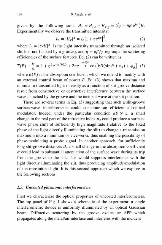
given by the following sum: � � �, � �,� � �!� � �� e� ".
Experimentally we observe the transmitted intensity:
#� � |�|% � #&'1 � )*� '%, (2)
where #& � |��|%
is the light intensity transmitted through an isolated
slit (i.e. not flanked by a groove), and ) � ��/� regroups the scattering
efficiencies of the surface features. Eq. (2) can be written as:
+,-. / 0102
� 1 � )%*34,5.6 � 2)*37,8.9: cos=��,sin � � �. � ��> (3)
where �,-. is the absorption coefficient which we intend to modify with
an external control beam of power -. Eq. (3) shows that maxima and
minima in transmitted light intensity as a function of slit-groove distance
result from constructive or destructive interference between the surface
wave launched by the groove and the incident wave at the slit position.
There are several terms in Eq. (3) suggesting that such a slit-groove
surface-wave interferometer could constitute an efficient all-optical
modulator. Indeed, under the particular condition �� ? 1, a small
change in the real part of the refractive index � could produce a surface-
wave phase shift of sufficiently high magnitude (relative to the fixed
phase of the light directly illuminating the slit) to change a transmission
maximum into a minimum or vice-versa, thus enabling the possibility of
phase-modulating a probe signal. In another approach, for sufficiently
long slit-groove distances �, a small change in the absorption coefficient
� could lead to substantial attenuation of the surface wave during its trip
from the groove to the slit. This would suppress interference with the
light directly illuminating the slit, thus producing amplitude-modulation
of the transmitted light. It is this second approach which we explore in
the following sections.
2.3. Uncoated plasmonic interferometers
First we characterize the optical properties of uncoated interferometers.
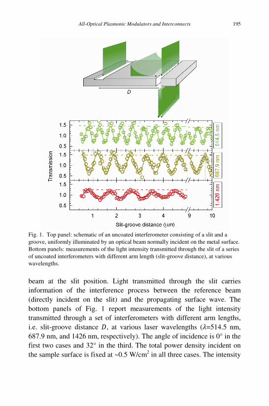
The top panel of Fig. 1 shows a schematic of the experiment; a single
interferometric device is uniformly illuminated by an optical Gaussian
beam. Diffractive scattering by the groove excites an SPP which
propagates along the metal/air interface and interferes with the incident
All-Optical Plasmonic Modulators and Interconnects
195
Fig. 1. Top panel: schematic of an uncoated interferometer consisting of a slit and a
groove, uniformly illuminated by an optical beam normally incident on the metal surface.
Bottom panels: measurements of the light intensity transmitted through the slit of a series
of uncoated interferometers with different arm length (slit-groove distance), at various
wavelengths.
beam at the slit position. Light transmitted through the slit carries
information of the interference process between the reference beam
(directly incident on the slit) and the propagating surface wave. The
bottom panels of Fig. 1 report measurements of the light intensity
transmitted through a set of interferometers with different arm lengths,
i.e. slit-groove distance �, at various laser wavelengths (�=514.5 nm,
687.9 nm, and 1426 nm, respectively). The angle of incidence is 0° in the
first two cases and 32° in the third. The total power density incident on
the sample surface is fixed at ~0.5 W/cm2 in all three cases. The intensity
D. Pacifici et al. 196
of light transmitted by an isolated reference slit is used to normalize the
transmission data through each device.
Compiling the normalized data yields a plot of normalized
transmitted intensity as a function of slit-groove distance (where each
open circle corresponds to a device with a specific slit-groove distance).
Several features are apparent in Fig. 1: (1) at a given incident free-space
wavelength �, the normalized transmission through the subwavelength
slit shows oscillatory behavior as a function of the slit-groove distance,
as a result of constructive or destructive interference between the
incident beam and the surface wave launched by the neighboring groove,
(2) the spatial period of this oscillation increases with increasing �, and
(3) the envelope of the oscillation amplitude remains approximately
constant as a function of interferometer arm length, suggesting that
within the investigated spectral range, surface waves can propagate for
several micrometers without significant loss.
The observed enhancement and suppression of the intensity
transmitted through the slit can be explained within the theoretical
framework developed in section 2.2. Using Eq. 3 with � � 2π/�, �, and
� as known parameters, fits are performed to the data reported in Fig. 1,
and shown as solid lines. These fits yield important physical parameters
such as the surface wave launching efficiency ), which is about 20-25%
in the investigated spectral range, the phase lag caused by diffraction at
the slit ��, which depends on groove depth and it is approximately �/2,
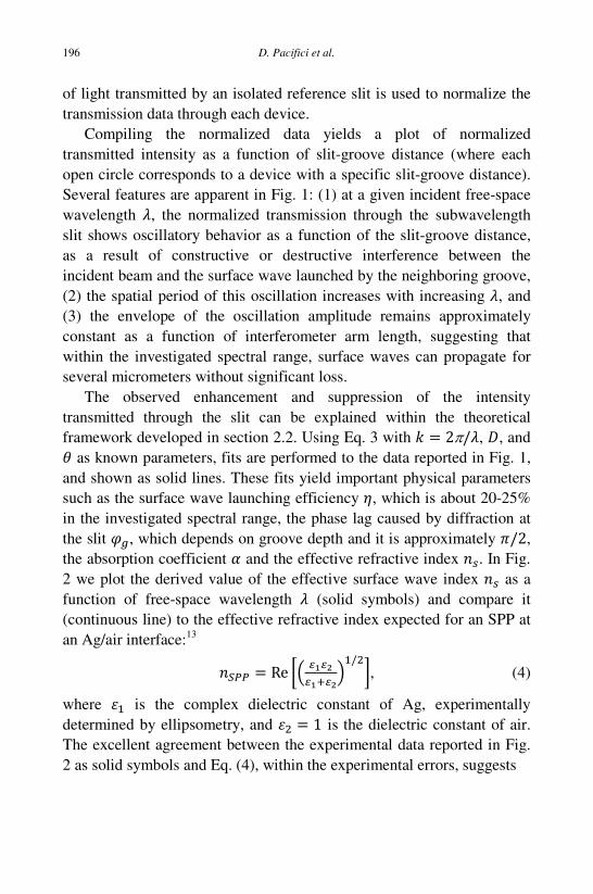
the absorption coefficient � and the effective refractive index �. In Fig.
2 we plot the derived value of the effective surface wave index � as a
function of free-space wavelength � (solid symbols) and compare it
(continuous line) to the effective refractive index expected for an SPP at
an Ag/air interface:13
�@55 � Re BC DED:DEFD:
GH/%I, (4)
where JH is the complex dielectric constant of Ag, experimentally
determined by ellipsometry, and J% � 1 is the dielectric constant of air.
The excellent agreement between the experimental data reported in Fig.
2 as solid symbols and Eq. (4), within the experimental errors, suggests
All-Optical Plasmonic Modulators and Interconnects
197
Fig. 2. Refractive index of the propagating surface wave modes as extracted by
transmission measurements through uncoated and QD-coated interferometers.
that the long-range propagating surface wave is indeed an SPP. This
demonstrates that diffractive scattering from a single subwavelength
groove in a metal film can be an efficient source of guided surface
plasmons at a metal-dielectric interface, indeed more compact than bulky
prism- or grating-coupling approaches.
2.4. QD-coated plasmonic interferometers
In order to actively modify the propagation constants of the SPP
launched by the groove, we coated the metal with a thin layer of
semiconductor quantum dots, as explained in the previous experimental
section.
As shown in Fig. 3, when excited by a laser beam at 404 nm the CdSe
QDs show bright PL peaked at 625 nm with a FWHM of 32 nm, and red-
shifted with respect to the 1S absorption edge which occurs at 595 nm, as
evidenced by the absorption curve reported in Fig. 3. This emissive state
is generally attributed to splitting of the lowest hole state as a result of
crystal field and e-h exchange interaction,29,30
as shown in the right inset

D. Pacifici et al. 198
Fig. 3. Absorption cross section (σ ) and photoluminescence spectrum (PL) for CdSe
QDs. Insets: energy level scheme for a QD.
to Fig. 3. Both the PL and the absorption of the CdSe QD ensemble show
broad features, indicating both homogeneous and inhomogeneous level
broadening caused by the crystal-field induced removal of level
degeneracy and by the size distribution of nanocrystals, respectively. It is
interesting to note that the CdSe QDs have relatively high absorption
cross section in the visible.31
For example the measured absorption cross
section at 514.5 nm is 3.5×10⁻¹⁵
cm2. This value is 6 orders of magnitude
higher than the typical absorption cross sections for atomic-like
transitions in rare-earth ions, which are extensively used in
telecommunication and as promising active materials in
microphotonics.32
To understand the role of the thin layer of CdSe QDs,
we performed transmission experiments on similar slit-groove
interferometers coated with QDs, and with varying arm distances. A
schematic of the transmission experiment is reported in the top panel of
Fig. 4. The normalized light intensities transmitted through the slit of
various interferometers are reported in the bottom panels of Fig. 4, as a
function of slit-groove separation distance, and at various free-space
wavelengths λ. The first interesting observation is that the transmission
maxima and minima occur at shorter slit-groove distances. This effect is
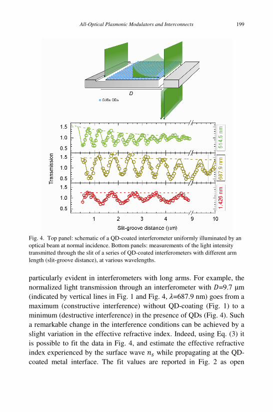
All-Optical Plasmonic Modulators and Interconnects
199
Fig. 4. Top panel: schematic of a QD-coated interferometer uniformly illuminated by an
optical beam at normal incidence. Bottom panels: measurements of the light intensity
transmitted through the slit of a series of QD-coated interferometers with different arm
length (slit-groove distance), at various wavelengths.
particularly evident in interferometers with long arms. For example, the
normalized light transmission through an interferometer with �=9.7 µm
(indicated by vertical lines in Fig. 1 and Fig. 4, �=687.9 nm) goes from a
maximum (constructive interference) without QD-coating (Fig. 1) to a
minimum (destructive interference) in the presence of QDs (Fig. 4). Such
a remarkable change in the interference conditions can be achieved by a
slight variation in the effective refractive index. Indeed, using Eq. (3) it
is possible to fit the data in Fig. 4, and estimate the effective refractive
index experienced by the surface wave � while propagating at the QD-
coated metal interface. The fit values are reported in Fig. 2 as open
D. Pacifici et al. 200
symbols. The SPP refractive index systematically increases relative to
the case of the uncoated interferometers, due to the presence of the high-
refractive index film of CdSe QDs. The increase is consistent with
calculations of the SPP mode profile and modal overlap with the CdSe
QD layer, whose refractive index was measured by spectroscopic
ellipsometry as a function of wavelength. We note that at �=1426 nm the
value of � is only marginally higher in the case of the coated sample
compared to that of the uncoated sample. At � = 514.5 nm, � is 6%
higher in the QD-coated interferometer, consistent with an increased
mode overlap with the QD layer due to the smaller skin depth of the SPP
at shorter wavelengths.
Another striking result arises from a close comparison between the
transmission data at �=514.5 nm in Fig. 4 and Fig. 1, that is the envelope
of the oscillating normalized transmission strongly decreases with slit-
groove distance in the presence of QDs (Fig. 4, �=514.5 nm), while it is
approximately constant for the uncoated sample (Fig. 1, �=514.5 nm).
The extracted absorption coefficient � increases from 400 cm-1
without
the QD layer to 8200 cm-1
with the QD layer. At first one may be
tempted to explain the increased absorption by out-of-plane scattering of
the SPP by the QDs. This hypothesis is easily ruled out by looking at the
transmission data at longer wavelengths. Since Rayleigh scattering
depends on the fourth power of the incident wavelength, one would
expect stronger absorption at longer wavelengths. However, the
oscillating transmission data at �=687.9 nm and �=1426 nm in Fig. 4
show a constant envelope amplitude as a function of slit-groove distance,
similar to the uncoated case, suggesting that no substantial absorption is
indeed occurring.
Instead, the increased absorption can be explained in terms of
plasmonic excitation of electron-hole pairs in the QDs. For a nanocrystal
radius of 2.4 nm, and a close-packed distribution of QDs, the estimated
QD concentration in the film is L~1× 10HO cm-3
. We estimate an SPP
mode overlap with the 24-nm thick CdSe film P~25%. Therefore, the
calculated effective absorption coefficient at �=514.5 nm would be
� � ΓRL � 8750 cm-1
. This value is in very good agreement with the
value (8200 cm-1
) extracted from the fitting procedure, and strongly
support the hypothesis that the QDs are indeed absorbing the propagating
All-Optical Plasmonic Modulators and Interconnects
201
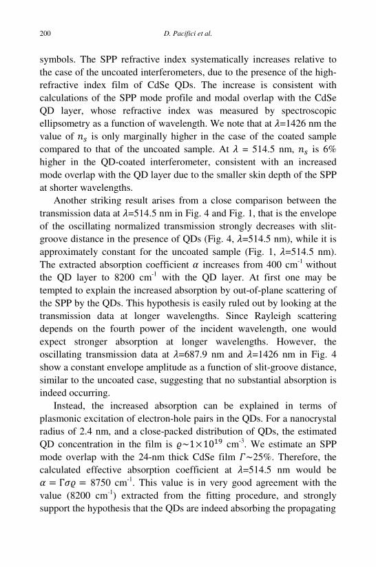
Fig. 5. Interferometry at λ=514.5 nm for QD-coated devices. Top panel: transmission
measurements for a series of QD-coated interferometers with different arm length (slit-
groove distance). Bottom panel: SPP intensity at the slit position as a function of slit-
groove distance.
SPP at �=514.5 nm. To stress this point, in Fig. 5 we report the
transmission data at �=514.5 nm for the QD-coated sample (top panel)
together with the extrapolated values of the SPP intensity measured at
the slit position (bottom panel), as a function of slit-groove distance. The
SPP intensity decreases exponentially with an experimental decay
constant (propagation length) S � 1.2 µm, again in good agreement with
the value estimated by assuming bandgap absorption in the QDs (which
gives �3H = 1.14µm). The emerging picture is therefore the following:
(1) SPPs with energy above the QD bandgap can be absorbed by CdSe
QDs while propagating along the metal/dielectric interface, with
subsequent photogeneration of bound electron-hole pairs (excitons) in
the QD volume, as shown in the schematic of Fig. 5; (2) for sufficiently
long interferometers, the SPP generated at the groove location can be
completely absorbed by the QDs, and is no longer able to reach the slit;
therefore, neither constructive nor destructive interference between the
SPP and the incident beam at the slit position can occur, and the
normalized transmission intensity tends to 1 (Fig. 4, λ=514.5 nm); (3)
SPPs having energy smaller than the QD bandgap cannot be absorbed by

D. Pacifici et al. 202
the nanocrystals, thus they can propagate without attenuation, reach the
slit and interfere with the incident beam, causing either constructive or
destructive interference at the slit output mouth.
2.5. All-optical modulation in QD-coated plasmonic interferometers
So far we have studied the optical properties of plasmonic
interferometers illuminated by a single light beam at a time. In all-optical
modulators, two different light beams are generally employed: one of the
two beams (control) is used to copy information onto the other (signal) at
a different wavelength. In order to achieve modulation, the two beams,
which are otherwise independent, need to be coupled by using some
nonlinearity of the medium in which they propagate. Our intent is to use
a control beam in the form of a propagating SPP to change the absorption
coefficient α for another co-propagating signal SPP at a different
frequency. The signal SPP interferes with the incident field at the slit,
and the total light intensity transmitted through the slit is given by Eq.
(3).
The exponential function of α provides for the necessary non-linear
interaction between the two co-propagating SPPs. We performed
continuous-wave pump (λ=514.5 nm, θ=0°) and probe (λ=1426 nm,
θ=32°) transmission measurements on various quantum-dot coated
interferometers. As illustrated in the schematic diagram of Colour plate
1(a), the control and signal beams simultaneously and uniformly impinge
on the sample surface and are scattered by the subwavelength groove
which launches two co-propagating SPPs with different energies
(represented in green and red, respectively) towards the slit. The SPP at
λ=514.5 nm is strongly absorbed by the CdSe QDs, while the SPP at
λ=1426 nm propagates without absorption in the absence of the pump
SPP. First we consider a structure with a slit-groove distance D=3.6 µm
which displays a relative maximum in normalized transmission intensity
at λ=1426 nm in absence of pump illumination (Fig. 4, λ=1426 nm). The
top panel of Colour plate 2 displays (open symbols) the normalized
transmission intensity of this device at λ=1426 nm as a function of the
pump power at λ=514.5 nm. Both probe and pump beams are chosen to
have TM polarization (H-field parallel to the slit and groove long axis).

All-Optical Plasmonic Modulators and Interconnects
203
The normalized transmitted probe intensity decreases as a function of
pump power, reaching a minimum at a power density of ~600 W/cm2,
and then slightly increases as the pump power is increased further. Since
the transmission enhancement for that particular device at zero pump
power results from constructive interference between the SPP and the
incident beam at the slit position, a decreased transmission can only be
explained by attenuation of the surface wave due to an absorption
process that is activated by the pump beam.
We propose that it is confined carrier absorption from excited CdSe
QDs which attenuates the probe surface wave at λ=1426nm. In this
model (schematic shown in the left inset of Colour plate 2) a confined
exciton is first generated in a CdSe QD by photo-absorption of a control
SPP at λ=514.5nm. The signal SPP at λ=1426 nm then re-excites the
exciton by bringing the electron into a higher lying energy level of the
QD, and is therefore absorbed. By increasing the pump power, a larger
fraction of QDs is excited, and as a consequence more probe SPPs are
absorbed. This phenomenon is analog to the free carrier absorption
(FCA) of photons propagating in bulk semiconductors where free
carriers are generated by thermal ionization of the dopants or by optical
excitation of electron-hole pairs. The dynamics of this mechanism have
been extensively studied in thick films of CdSe QDs by femtosecond
transient absorption spectroscopy in the visible and near-infrared spectral
ranges.33,34
If we denote with RTTU the cross section for the confined carrier
absorption of a propagating signal SPP by an excited QD, the
photoinduced absorption coefficient is then equal to:
� � PσTTUVW. (5)
with P the mode overlap of the signal SPP with the active layer, and VW
the density of excited quantum dots in steady state. Approximating the
QD with a two-level system, VW is given by the following equation:
VW � σφτ
σφτFH V, (6)
where V is the total concentration of QDs in the film, φ is the fraction of
control SPP flux parallel to the metal/dielectric interface overlapping
with the active film (in cm-2
s-1
), σ the QD absorption cross section at the

D. Pacifici et al. 204
pump wavelength, and τ the recombination lifetime of an excited QD. In
the low pump power regime, such that σφτ X 1, Eq. (6) becomes:
VW � σφτ V, (7)
where φ can be calculated using the Poynting theorem and integrating the
magnitude of the Poynting vector over the active region. Without loss of
generality, φ is a linear function of the incident pump power density -:
φ � )Y5Z, (8)
with )Y an effective coefficient taking into account the incoupling
efficiency, scattering cross section of the groove, and mode overlap of
the control SPP with the active layer, and [ � \] the energy of an SPP of
frequency ] � ^/�, with \ and ^ the Planck’s constant and speed of
light, respectively.
By combining the previous equations, Eq. (5) becomes:
�,-. � )YPσTTUστ V _`Y -, (9)
which proves that �,-. is a linear function of the incident pump power
density -.
To demonstrate that the observed all-optical modulation of light
intensity at λ=1426 nm transmitted through the slit results solely from
excitation of the CdSe QDs by the control SPP at λ=514.5 nm and not
from direct illumination of the QDs by the incident pump beam, we
changed the polarization of the pump beam at λ=514.5 nm from TM to
TE (electric field parallel to the slit and groove long axis), a polarization
for which no surface wave can be launched by the groove or the slit.
When the two-colour pump-probe experiment is repeated under these
conditions as a function of pump power (Colour plate 2, solid symbols),
no significant modulation of transmitted intensity is observed as a
function of pump power.
The lack of transmission modulation in absence of the surface wave
shows that direct illumination of the surface is a negligible source of QD
excitation over the explored range of pump powers. This is not surprising
since the sum of the incident and reflected fields has, at normal
incidence, a node at the metal-air interface, leading to a negligible
contribution to optical power density in the CdSe-QD layer. On the other
hand, the field amplitude of the control SPP launched by the groove has a
All-Optical Plasmonic Modulators and Interconnects
205
maximum right at the interface, guaranteeing maximum mode overlap
with the active QD layer. We conclude that the large amplitude
transmission modulation observed in the case of a TM-polarized pump
beam is the direct result of excitation of the CdSe QDs by a surface wave
at that frequency launched by the groove and the slit.
For an interferometer with aperture-groove distance D=2.15 µm a
transmission minimum occurs at λ=1426 nm, as shown in Fig. 4. The
probe transmission variation with pump power through this particular
device is given in the bottom panel of Colour plate 2. Unlike the
variation observed for a distance corresponding to a transmission
maximum, the intensity increases as a function of pump power density
and then starts to decrease again with increasing pump power. In this
case, photoinduced absorption of the probe SPP reduces its destructive
interference with the incident beam at the slit, and thus increases the
overall normalized transmission, making it closer to that of an isolated
slit, i.e. equal to 1.
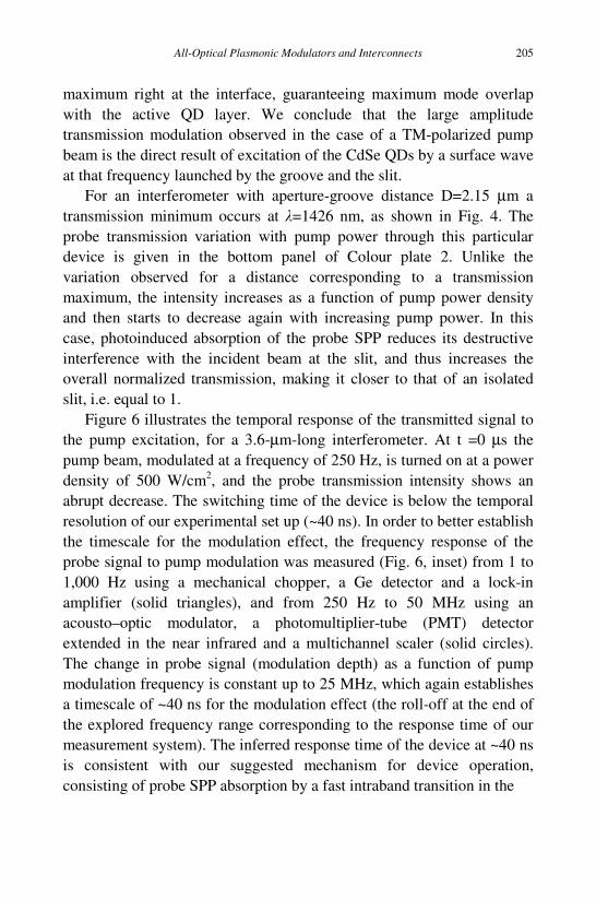
Figure 6 illustrates the temporal response of the transmitted signal to
the pump excitation, for a 3.6-µm-long interferometer. At t =0 µs the
pump beam, modulated at a frequency of 250 Hz, is turned on at a power
density of 500 W/cm2, and the probe transmission intensity shows an
abrupt decrease. The switching time of the device is below the temporal
resolution of our experimental set up (~40 ns). In order to better establish
the timescale for the modulation effect, the frequency response of the
probe signal to pump modulation was measured (Fig. 6, inset) from 1 to
1,000 Hz using a mechanical chopper, a Ge detector and a lock-in
amplifier (solid triangles), and from 250 Hz to 50 MHz using an
acousto–optic modulator, a photomultiplier-tube (PMT) detector
extended in the near infrared and a multichannel scaler (solid circles).
The change in probe signal (modulation depth) as a function of pump
modulation frequency is constant up to 25 MHz, which again establishes
a timescale of ~40 ns for the modulation effect (the roll-off at the end of
the explored frequency range corresponding to the response time of our
measurement system). The inferred response time of the device at ~40 ns
is consistent with our suggested mechanism for device operation,
consisting of probe SPP absorption by a fast intraband transition in the
D. Pacifici et al. 206
Fig. 6. Variation of the probe intensity transmitted through the slit of a 3.6-µm-long
interferometer as a function of time; at t=0 µs the pump beam is turned on, and a fast
(<40 ns) decrease in probe transmitted intensity is observed, due to photoinduced
absorption in excited QDs. Inset: variation of the probe signal as a function of pump
beam modulation frequency, at a power level of 500 W/cm2.
CdSe QDs excited by the control SPP. The data reported in Fig. 6 clearly
demonstrate the possibility of achieving modulation frequencies that are
orders of magnitude faster than typical frequency responses of
modulators relying on thermal effects, which are typically in the range of
a few Hz. At power densities >600 W cm2, both interferometers shown in
Colour plate 2 experience a recovery of their original (that is, zero-pump)
transmission values, owing to a reduction in absorption of the probe SPP
from excited QDs.
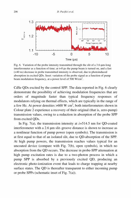
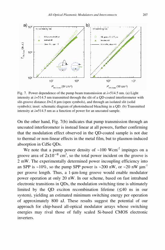
In Fig. 7(a), the transmission intensity at λ=514.5 nm for QD-coated
interferometer with a 2.6 µm slit–groove distance is shown to increase as
a nonlinear function of pump power (open symbols). The transmission is
at first equal to that of an isolated slit, due to QD-absorption of the SPP.
At high pump powers, the transmission reaches values typical for an
uncoated device (compare with Fig. 7(b), open symbols), in which no
absorption from the QD occurs. The decrease in probe-SPP attenuation at
high pump excitation rates is due to a two-photon process in which a
pump SPP is absorbed by a previously excited QD, producing an
electronic photo-ionization event that leads to charge trapping at nearby
surface states. The QD is thereafter transparent to either incoming pump
or probe SPPs (schematic inset of Fig. 7(a)).
All-Optical Plasmonic Modulators and Interconnects
207
Fig. 7. Power dependence of the pump beam transmission at λ=514.5 nm. (a) Light
intensity at λ=514.5 nm transmitted through the slit of a QD-coated interferometer with
slit-groove distance D=2.6 µm (open symbols), and through an isolated slit (solid
symbols); inset: schematic diagram of photoinduced bleaching in a QD. (b) Transmitted
intensity at λ=514.5 nm as a function of power for an uncoated sample.
On the other hand, Fig. 7(b) indicates that pump transmission through an
uncoated interferometer is instead linear at all powers, further confirming
that the modulation effect observed in the QD-coated sample is not due
to thermal or non-linear effects in the metal film, but to plasmon-induced
absorption in CdSe QDs.
We note that a pump power density of ~100 Wcm-2
impinges on a
groove area of 2x10³b cm2, so the total power incident on the groove is
2 mW. The experimentally determined power incoupling efficiency into
an SPP is ~10%, so the pump SPP power is ~200 nW, or ~20 nW µm-1
per groove length. Thus, a 1-µm-long groove would enable modulator
power operation at only 20 nW. In our scheme, based on fast intraband
electronic transitions in QDs, the modulation switching time is ultimately
limited by the QD exciton recombination lifetime (c40 ns in our
system), yielding an estimated minimum switching energy per operation
of approximately 800 aJ. These results suggest the potential of our
approach for chip-based all-optical modulator arrays whose switching
energies may rival those of fully scaled Si-based CMOS electronic
inverters.
D. Pacifici et al. 208
3. Three-dimensional plasmonic modulators
3.1. New designs for improved figures of merit
In 2005, the ITRS set the requirements for a basic all-optical switching
element, namely: it should (1) work at around 1.5 µm, (2) operate at low
power, and (3) have a small component size. The planar interferometers
presented so far are interesting because they fulfill all of these
requirements. Nevertheless, the proof-of-concept design is affected by
some important drawbacks that we would like to address and overcome.
First of all, even though the planar interferometers are characterized by a
fast switching time and high modulation frequency, the typical
modulation depth is relatively small, of the order of only ~10-20%. This
is determined by the fact that even though the signal SPP is completely
extinguished by photoinduced absorption in excited QDs, the light
transmitted through the slit can never be zero, since the slit is always
illuminated by the incident beam. A way to overcome this problem
maintaining the same geometry would be to use localized excitation
sources, such as the subwavelength aperture of a near-field optical
microscope, to illuminate the groove and not the slit. In such a way,
when the probe beam is on, the transmission through the slit is
determined only by the propagating SPP term, i.e. � � �,� ��!�� *� ", since the slit contribution is now �, � 0. The normalized
transmission in this case would be:
+,-. / 01,5.01,5d&. � |e1,5.|:
|e1,5d&.|: � *34,5.6, (10)
where we have explicitly considered the power dependence of the
absorption coefficient. In the absence of pump power, that is - � 0,
�,-.� X 1 and the normalized transmission through the slit is equal to
“1,” corresponding to the “on” state of the device. As soon as the pump
beam is turned on, and the power set such that �,-.� ? 1, the signal
SPP is completely absorbed by the excited QDs. Therefore no signal SPP
can reach the slit, which in turn reduces the transmitted intensity to zero.
Such a strategy would certainly enable orders of magnitude increase in
modulation depth. However, this approach is not easy to implement in
integrated dense optical chips.
All-Optical Plasmonic Modulators and Interconnects
209
Therefore, in order to solve the problem in a way that may lead to
more realistic architectures, we designed and fabricated a novel
plasmonic modulator, whose schematic and principle of operation are
reported in Colour plate 3. The interferometer consists of a
metal/dielectric/metal waveguide, and makes use of two slits milled in
the top metal layer to incouple the incident beam into SPPs propagating
in the dielectric waveguide. The dielectric can be a semiconductor, or
even an insulating matrix codoped with CdSe quantum dots. By
opportunely choosing its thickness, the dielectric layer can be made to
only support the fundamental plasmonic mode while cutting-off all of the
higher order photonic modes. A slit in the bottom metal layer collects the
propagating SPPs; the interfered field is then guided in the slot cavity
provided by the slit and scattered back in free space, at the bottom side of
the device. It is interesting to note that this design could be merged with
modern microelectronic circuits, by simply placing a CMOS-based
detector right at the bottom output of the out-coupling slit. The device
depicted in Colour plate 3 resembles a miniaturized Mach-Zehnder
interferometer, with arms A and B, having lengths �U and �f,
respectively. When the two input slits are coherently and uniformly
illuminated with a signal beam at normal incidence, SPPs with field
amplitudes @55,U and @55,f are launched and guided into the dielectric
waveguide with the same amplitude � and the same incoupling phase
lag �& (analogous to �� in Eq.(1)); the SPPs propagate with wavevector
�@55 � �@55� and reach the outcoupler slit with a relative phase shift:
∆� � �U h �f � C�@55 � � 4,5.% G ,�U h �f., (11)
which determines the interference condition between the two SPPs at the
output slit position. For interferometers with relatively small arms, the
material loss in the absence of pump power is negligible, and we can
safely assume �,- � 0. � 0 in Eq. (11). The same arguments holds true
if we choose the difference in optical path such that �,- � 0.,�U h�f. X 1. Either way, in the absence of a pump beam, by setting the
distance of the two arms of the interferometer in such a way that the two
SPPs are exactly out of phase, that is ∆� � �, the two SPPs perfectly
cancel out at the slit position, thus determining an exact null in
transmitted intensity through the bottom slit; this is the “off” state of the
modulator. The condition for destructive interference can be altered by
D. Pacifici et al. 210
affecting the propagation of the SPP in one of the two arms using a pump
SPP. For example, we could excite a control SPP in one of the two arms,
say arm B, which would induce free-carrier absorption of the signal SPP
propagating in arm B. This in turn would prevent the destructive
interference with the other signal SPP propagating in arm A, which
would then be transmitted through the slit, determining the “on” state of
the modulator.
Another drawback of the simple planar proof-of-concept approach
previously investigated in section 2 is that the control and signal SPPs
are excited using the same subwavelength object (a groove), co-
propagate in the modulator and are simultaneously transmitted through
the slit. For many applications it would be desirable to maintain optical
isolation between the two beams. Typically, this can be accomplished by
using a filter in the far field to selectively transmit the frequency of
interest. This approach is of course not convenient for large scale
integration of the device. Therefore we recur to another trick.
Subwavelength slits are very good polarizers, in that they can only
transmit light with H-field component parallel to their long-axis (TM-
polarized beam). At the same time, the launching efficiency for long-
range propagating SPPs is maximum when the slit is illuminated with
TM-polarized beams, and it goes to zero for TE-polarized beams.
Therefore, to achieve the desired isolation, we use cross-polarized signal
and control beams, and slits that are perpendicular to each other to
independently incouple signal and control SPPs, respectively.
A practical implementation of the Mach-Zehnder plasmonic
interferometer consists of two thermally evaporated 300-nm-thick silver
films separated by a core layer of SiO2 codoped with chemically
synthesized CdSe colloidal quantum dots (QDs), capped with a different
ligand (tris-hydroxylpropylphospine, THPP) to make them soluble in the
spin-on-glass matrix. The size of these QDs is engineered such that in the
ground state the QDs are transparent to the probe light, but once an
exciton is created, the QDs can absorb the probe. Several devices have
been fabricated by sequential evaporation of metal films, spin-coating of
spin-on-glass codoped with QDs, and focused ion beam milling. Parallel
slits are milled in the top and bottom silver films and aligned to
previously milled slits in the bottom metal layer. To selectively create
All-Optical Plasmonic Modulators and Interconnects
211
excitons only in one arm, slits parallel to the interferometer arm B are
milled by FIB on the top metal layer. Pump light cross-polarized with
respect to the probe beam is selectively coupled into this arm only.
An SEM micrograph of an array of 9 plasmonic Mach-Zehnder
interferometers is shown in Colour plate 4(a). In this array, the length of
arm A is varied from 2 µm (bottom device) to 2.4 µm (top device). A
cross section of one of the devices is shown in Colour plate 4(b). Smooth
core-cladding interfaces are clearly present, preventing SPPs from
scattering loss in the waveguide. Colour plates 4(b) and (c) show,
superimposed to the SEM micrographs, the working principle of the
proposed modulator. In Colour plate 4(b) the device is uniformly
illuminated with a probe beam, TM polarized, that is with magnetic field
oscillating parallel to the long axis of the incoupling slits. Since the top
metal layer is optically thick, light can only be transmitted through the
two slits which act as the mirrors of the interferometer. Light transmitted
through each slit is then coupled into SPPs propagating to the left and
right of each slit.
We focus our attention on the SPPs that propagate toward the output
slit milled in the bottom metal layer. By opportunely choosing the length
of the two interferometric arms (designated with A and B in Colour plate
3) a destructive interference can be set such that the light intensity
transmitted through the outcoupling slit is zero, or a minimum value.
This scenario represents the “off” state of the modulator, which would
correspond to a logic state “0.” In Colour plate 4(c) the device is also
illuminated with a pump beam which is cross-polarized with respect to
the probe signal. Light can leak through the vertically aligned slits which
act as sources of SPPs which propagate in the direction perpendicular to
the right arm of the interferometer (arm B in Colour plate 3). These SPPs
act as control beams in that they excite the QDs present in the dielectric
and determine a photo-induced absorption of the probe SPP, as explained
in section 2 for planar plasmonic interferometers. The signal SPP
propagating in the right arm of the interferometer is absorbed along its
path by free-carrier absorption in the excited QDs and is no longer able
to reach the output slit. Therefore the destructive interference with the
SPP propagating in the left arm is no longer possible. Light can now
emerge through the slit, and the state of the modulator is set to “on,”
D. Pacifici et al. 212
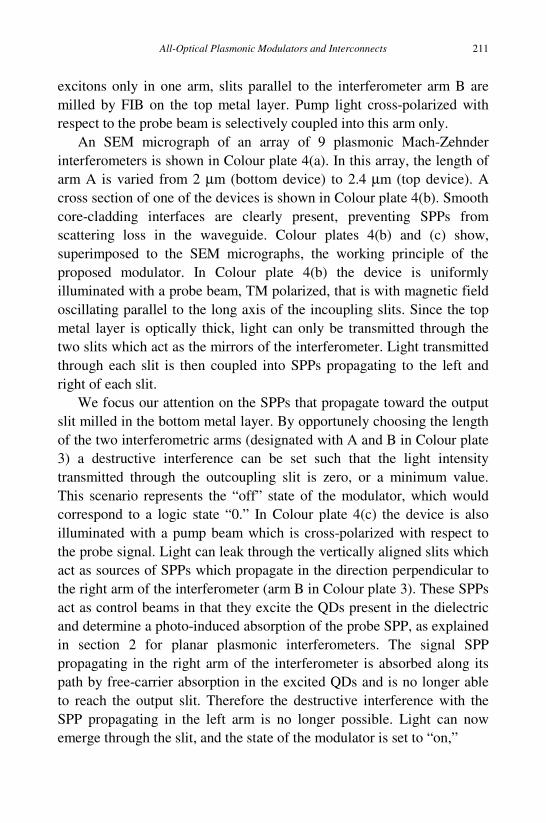
Fig. 8. Pump-power dependence of the transmitted probe intensity at 687.9 nm through a
plasmonic modulator that shows a minimum in probe transmission at zero pump power.
The solid line is a guide to the eye.
(logic state “1”). It is important to stress that the control SPPs are
characterized by a longitudinal electric field oscillating in the direction
parallel to the long axis of the output slit. For this polarization, no
transmission of the pump beam is observed through the slit, which
guarantees optical isolation between the control and the signal beams.
We experimentally investigate the operation of such interferometers
by performing pump and probe experiments. First, the probe
transmission trough the Mach-Zehnder plasmonic interferometers is
studied as a function of the length of interferometer arm A. In practice,
we scan the length of one of the two interferometer arms (arm A in this
case) and look for a device that shows a minimum in transmission. When
this condition is satisfied, destructive interference between the two SPPs
is taking place at the slit. We find that a destructive interference state is
obtained for a device with an interferometer arm length �U � 2.55µm.
Results of pump-probe experiments for such a device are presented in
Fig. 8. Simultaneous illumination with both pump and probe light beams
results in an increase of the transmitted probe intensity. By varying the
All-Optical Plasmonic Modulators and Interconnects
213
power density, the probe signal transmission at 687.9 nm increases up to
60% with respect to the zero-pump value, as the result of increased
absorption of the signal SPP propagating in the right arm of the
interferometer.
4. Design of plasmonic modulators and interconnects
Inspired by the previous experimental results, we employ finite-
difference time domain (FDTD) simulations to evaluate the performance
of higher complexity plasmonic waveguide structures which are not
readily tractable by analytic methods.
4.1. Multilevel plasmonic modulators and interconnects
In the following section, we study a multilayer metal/dielectric stack
which defines two horizontal dielectric waveguides, separated from each
other by a 150-nm-thick layer of Ag cladding. The cladding metal layer
is thick enough to be optically opaque, thus suppressing crosstalk due to
mode coupling between the top and bottom waveguides. Slits milled in
the central metal cladding play the role of optical “vias” between the two
dielectric waveguides. A subwavelength slit in the top metal layer acts as
optical incoupler in the first waveguide, and three slits milled in the
bottom metal layer serve as optical outcouplers. All the slits are 50 nm
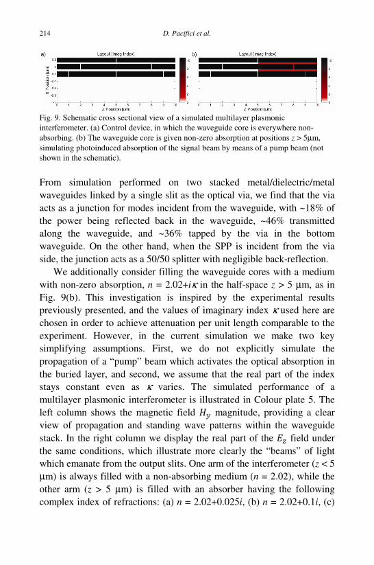
wide. A schematic cross section of the structure is reported in Fig. 9(a).
When illuminated by an optical beam, the slit in the top metal layer is
found to be effective at scattering light into guided modes of the first
buried metal/dielectric/metal waveguide. These guided modes are
launched with propagation direction transverse to the slit long axis. Two
slits in the central metal layer partially scatter the guided modes into
guided modes of the underlying waveguide. The waveguide dielectric
cores are here modeled as a purely transparent dielectric with n =
(2.02+0i), corresponding to that of QD-doped silicon dioxide at the
excitation wavelength λ = 1.5 µm. The relative fraction of light which is
“tapped” off by the via can be adjusted by varying the via width, or by
fabricating the via in a manner that provides dielectric contrast relative to
the core material.
D. Pacifici et al. 214
Fig. 9. Schematic cross sectional view of a simulated multilayer plasmonic
interferometer. (a) Control device, in which the waveguide core is everywhere non-
absorbing. (b) The waveguide core is given non-zero absorption at positions z > 5µm,
simulating photoinduced absorption of the signal beam by means of a pump beam (not
shown in the schematic).
From simulation performed on two stacked metal/dielectric/metal
waveguides linked by a single slit as the optical via, we find that the via
acts as a junction for modes incident from the waveguide, with ~18% of
the power being reflected back in the waveguide, ~46% transmitted
along the waveguide, and ~36% tapped by the via in the bottom
waveguide. On the other hand, when the SPP is incident from the via
side, the junction acts as a 50/50 splitter with negligible back-reflection.
We additionally consider filling the waveguide cores with a medium
with non-zero absorption, n = 2.02+iκ in the half-space z > 5 µm, as in
Fig. 9(b). This investigation is inspired by the experimental results
previously presented, and the values of imaginary index κ used here are
chosen in order to achieve attenuation per unit length comparable to the
experiment. However, in the current simulation we make two key
simplifying assumptions. First, we do not explicitly simulate the
propagation of a “pump” beam which activates the optical absorption in
the buried layer, and second, we assume that the real part of the index
stays constant even as κ varies. The simulated performance of a
multilayer plasmonic interferometer is illustrated in Colour plate 5. The
left column shows the magnetic field i magnitude, providing a clear
view of propagation and standing wave patterns within the waveguide
stack. In the right column we display the real part of the jk field under
the same conditions, which illustrate more clearly the “beams” of light
which emanate from the output slits. One arm of the interferometer (z < 5
µm) is always filled with a non-absorbing medium (n = 2.02), while the
other arm (z > 5 µm) is filled with an absorber having the following
complex index of refractions: (a) n = 2.02+0.025i, (b) n = 2.02+0.1i, (c)
All-Optical Plasmonic Modulators and Interconnects
215
n = 2.02+1.0i. The device is illuminated by a plane wave inciden7t on the
top input slit and produces three output beams through slits in the bottom
metal surface. As absorption is increased, the right output beam is
entirely suppressed, the center output beam is diminished, and the left
output beam is unchanged.
4.2. Incoupling strategies
In order to consider integration of our plasmonic modulators or other
subwavelength active devices as constituents of dense subwavelength
photonic networks, we must also address strategies for efficiently
coupling light in the plasmonic waveguides, and develop design
strategies to achieve low overall loss. In this section, we employ FDTD
simulations to survey alternative coupling schemes which are achievable
with minimal incremental changes to the device structures we have
already fabricated. In view of an increased compatibility with the
existing Si-based microphotonics and mature CMOS technology, we
investigated metal/dielectric/metal stack consisting of a core of 160-nm-
thick Si layer, with 10-nm-thick silicon dioxide, which may be codoped
with an active material, such as CdSe or Si QDs, showing photoinduced
carrier absorption for the signal SPP. As cladding layer we consider 400-
nm-thick Ag films on both sides of the thin waveguide. In all simulations
the incident light is TM polarized, monochromatic, continuous wave
excitation at λ = 1.55 µm. In the chosen coordinate system the waveguide
propagation axis is z. In all cases the input port, whether slit or
waveguide end facet, is centered at the center of the simulation volume,
with coordinates (z, x) = (2, 0) µm. At steady-state, the power which is
considered “incoupled” in the plasmonic waveguide is that which passes
through a monitor port consisting of a line segment which intersects the
waveguide axis at (z, x) = (2.5; -0.4:0.4) µm.
The following incoupling geometries are considered:
(1) Slit incoupling (Colour plate 6). The source is a gaussian beam with
1.5-µm waist in the plane x = 1 µm, about a half micrometer above the
surface. The slit is an air-filled opening transverse to the waveguide,
400 nm wide, 490 nm deep through the metal cladding and halfway into
the Si core. Note that the assumption that the focal radius equals λ is
D. Pacifici et al. 216
somewhat arbitrary but intended as a “best case” estimate. The reported
incoupling coefficient represents the energy coupled into the dielectric
waveguide in the +z direction; due to the symmetry of this coupling
scheme, of course the same amount also couples into the -z direction.
(2) Metal-clad taper incoupling (Colour plate 7). The source is the
lowest order TM mode of an air-clad Si-core waveguide with a 970-nm
thick core, same thickness as the entire stack. This waveguide is joined to
the 160-nm-thick Si core of the metal/dielectric/metal stack by a 1 µm
segment of concave parabolic taper. The tapered segment is clad in Ag.
(3) Thin (160 nm) waveguide incoupling (Colour plate 8). The source
is the lowest order TM mode of a 160-nm-thick Si waveguide in air.
For comparison, we also consider a tapered waveguide incoupling
geometry where the source is the lowest order TM mode of an air-clad
Si-core waveguide with a 970-nm-thick core, joined to the 170-nm-thick
Si core of the metal/dielectric/metal stack by a 1 µm segment of concave
parabolic taper, clad in air; and to conclude, end-fire incoupling by using
a gaussian beam with 1.5-µm waist, incident normal to the end facet of
an abruptly truncated metal/dielectric/metal waveguide. The results of
the FDTD data analysis are reported in Table 1.
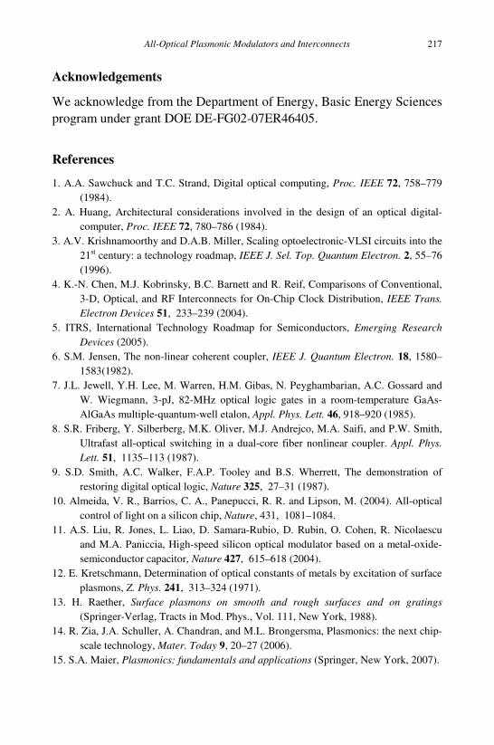
We find that the insertion loss for the 160-nm-waveguide end-fire
scheme, Table 1, is only -4.4 dB, an improvement of about 8 dB over the
slit-coupling geometry. This type of analysis allows us to trade off the
demand for increased performance with the desire to minimize added
design complexity. Most importantly, the substantial improvement
reported here can be achieved without varying the width of the Si core in
the dielectric waveguide region relative to that of the core in the
metal/dielectric/metal active region.
Table 1. Power incoupled to Ag/Si/Ag plasmonic waveguide.
Incoupling Geometry Incoupled Power Incoupled Power
(%) (dB)
Slit 5.2 -12.8
Endfire 14.8 -8.3
Air-clad taper 20.4 -6.9
Metal-clad taper 24.0 -6.2
Thin (160 nm) waveguide 35.9 -4.4
All-Optical Plasmonic Modulators and Interconnects
217
Acknowledgements
We acknowledge from the Department of Energy, Basic Energy Sciences
program under grant DOE DE-FG02-07ER46405.
References
1. A.A. Sawchuck and T.C. Strand, Digital optical computing, Proc. IEEE 72, 758–779
(1984).
2. A. Huang, Architectural considerations involved in the design of an optical digital-
computer, Proc. IEEE 72, 780–786 (1984).
3. A.V. Krishnamoorthy and D.A.B. Miller, Scaling optoelectronic-VLSI circuits into the
21st century: a technology roadmap, IEEE J. Sel. Top. Quantum Electron. 2, 55–76
(1996).
4. K.-N. Chen, M.J. Kobrinsky, B.C. Barnett and R. Reif, Comparisons of Conventional,
3-D, Optical, and RF Interconnects for On-Chip Clock Distribution, IEEE Trans.
Electron Devices 51, 233–239 (2004).
5. ITRS, International Technology Roadmap for Semiconductors, Emerging Research
Devices (2005).
6. S.M. Jensen, The non-linear coherent coupler, IEEE J. Quantum Electron. 18, 1580–
1583(1982).
7. J.L. Jewell, Y.H. Lee, M. Warren, H.M. Gibas, N. Peyghambarian, A.C. Gossard and
W. Wiegmann, 3-pJ, 82-MHz optical logic gates in a room-temperature GaAs-
AlGaAs multiple-quantum-well etalon, Appl. Phys. Lett. 46, 918–920 (1985).
8. S.R. Friberg, Y. Silberberg, M.K. Oliver, M.J. Andrejco, M.A. Saifi, and P.W. Smith,
Ultrafast all-optical switching in a dual-core fiber nonlinear coupler. Appl. Phys.
Lett. 51, 1135–113 (1987).
9. S.D. Smith, A.C. Walker, F.A.P. Tooley and B.S. Wherrett, The demonstration of
restoring digital optical logic, Nature 325, 27–31 (1987).
10. Almeida, V. R., Barrios, C. A., Panepucci, R. R. and Lipson, M. (2004). All-optical
control of light on a silicon chip, Nature, 431, 1081–1084.
11. A.S. Liu, R. Jones, L. Liao, D. Samara-Rubio, D. Rubin, O. Cohen, R. Nicolaescu
and M.A. Paniccia, High-speed silicon optical modulator based on a metal-oxide-
semiconductor capacitor, Nature 427, 615–618 (2004).
12. E. Kretschmann, Determination of optical constants of metals by excitation of surface
plasmons, Z. Phys. 241, 313–324 (1971).
13. H. Raether, Surface plasmons on smooth and rough surfaces and on gratings
(Springer-Verlag, Tracts in Mod. Phys., Vol. 111, New York, 1988).
14. R. Zia, J.A. Schuller, A. Chandran, and M.L. Brongersma, Plasmonics: the next chip-
scale technology, Mater. Today 9, 20–27 (2006).
15. S.A. Maier, Plasmonics: fundamentals and applications (Springer, New York, 2007).
D. Pacifici et al. 218
16. H.A. Atwater, The promise of plasmonics, Sci. Am. 296, 56–63 (2007).
17. F.J. Garcìa-Vidal, H.J. Lezec, T.W. Ebbesen, and L. Martin-Moreno, Multiple paths
to enhance optical transmission through a single subwavelength slit, Phys. Rev.
Lett. 90, 213901 (2003).
18. H.J. Lezec, and T. Thio, Diffracted evanescent wave model for enhanced and
suppressed optical transmission through subwavelength hole arrays, Opt. Express
12, 3629–3651 (2004).
19. H.F. Schouten, N. Kuzmin, G. Dubois, T.D. Visser, G. Gbur, P.F.A. Alkemade, H.
Blok, G.W. ‘t Hooft, D. Lenstra, E.R. Eliel, Plasmon-assisted two-slit
transmission: Young's experiment revisited, Phys. Rev. Lett. 94, 053901 (2005).
20. P. Lalanne, J.P. Hugonin and J.C. Rodier, Theory of surface plasmon generation at
nanoslit apertures, Phys. Rev. Lett. 95, 263902 (2005).
21. G. Gay, O. Alloschery, B. Viaris de Lesegno, C. O’Dwyer, J. Weiner and H.J. Lezec,
The optical response of nanostructured surfaces and the composite diffracted
evanescent wave model, Nature Phys. 2, 262–267 (2006).
22. G. Gay, O. Alloschery, B. Viaris de Lesegno, J. Weiner, and H.J. Lezec, Surface
wave generation and propagation on metallic subwavelength structures measured
by far-field interferometry, Phys. Rev. Lett. 96, 213901 (2006).
23. O.T.A. Janssen, H.P. Urbach, and G.W. ‘t Hooft, On the phase of plasmons excited
by slits in a metal film, Opt. Express 14, 11823–11832 (2006).
24. D. Pacifici, H.J. Lezec, H.A. Atwater and J. Weiner, Quantitative determination of
optical transmission through subwavelength slit arrays in Ag films: Role of surface
wave interference and local coupling between adjacent slits, Phys. Rev. B 77,
115411 (2008).
25. D. Pacifici, H.J. Lezec and H.A. Atwater, All-optical modulation by plasmonic
excitation of CdSe quantum dots, Nature Photon. 1, 402–406 (2007).
26. G. Lévêque, O.J.F. Martin, J. Weiner, Transient behavior of surface plasmon
polaritons scattered at a subwavelength groove, Phys. Rev. B 76, 155418 (2007).
27. J. Weiner, Phase shifts and interference in surface plasmon polariton waves, Opt.
Express 16, 950–956 (2008).
28. C.B. Murray, D.J. Noms, and M.G. Bawendi, Synthesis and characterization of nearly
monodisperse CdE (E = S, Se, Te) semiconductor nanocrystallites, J. Am. Chem.
Soc. 115, 8706–8715 (1993).
29. M. Nirmal, D.J. Norris, M. Kuno, M.G. Bawendi, A.L. Efros and M. Rosen,
Observation of the dark exciton in CdSe quantum dots, Phys. Rev. Lett. 75, 3728–
3731 (1995).
30. V.I. Klimov, A.A. Mikhailovsky, S. Xu, A. Malko, J.A. Hollingsworth, C.A.
Leatherdale, H.J. Eisler and M.G. Bawendi, Optical gain and stimulated emission
in nanocrystal quantum dots, Science 290, 314–317 (2000).
31. C.A. Leatherdale, W.-K. Woo, F.V. Mikulec and M.G. Bawendi, On the absorption
cross section of CdSe nanocrystal quantum dots, J. Phys. Chem. B 106, 7619–7621
(2002).

All-Optical Plasmonic Modulators and Interconnects
219
32. A. Polman, Erbium implanted thin film photonic materials, J. Appl. Phys. 82, 1–39
(1997).
33. V.I. Klimov, C.J. Schwarz, D.W. McBranch, C.A. Leatherdale and M.G. Bawendi,
Ultrafast dynamics of inter- and intraband transitions in semiconductor
nanocrystals: Implications for quantum-dot lasers, Phys. Rev. B 60, R2177–R2180
(1999).
34. V.I. Klimov, Optical nonlinearities and ultrafast carrier dynamics in semiconductor
nanocrystals, J. Phys. Chem. B 104, 6112–6123 (2000).


![Enhancing the Angular Sensitivity of Plasmonic Sensors ...biotheory.phys.cwru.edu/PDF/AOM.pdf · ultrasensitive plasmonic biosensors.[29,30] A plasmonic nanorod metamaterial (Type](https://img.pdfslide.us/doc/110x75/5fcdd2c6db367d06a677e7be/enhancing-the-angular-sensitivity-of-plasmonic-sensors-ultrasensitive-plasmonic.jpg)