Embed Size (px)
Citation preview
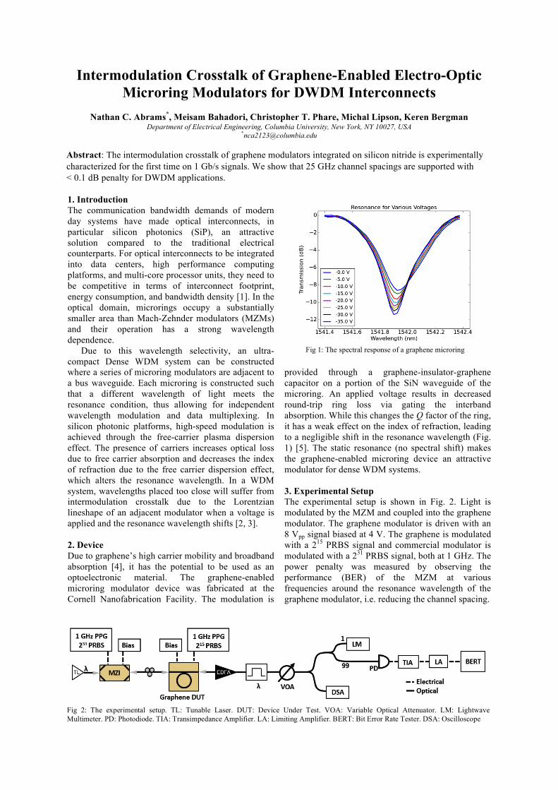
Fig 2: The experimental setup. TL: Tunable Laser. DUT: Device Under Test. VOA: Variable Optical Attenuator. LM: Lightwave Multimeter. PD: Photodiode. TIA: Transimpedance Amplifier. LA: Limiting Amplifier. BERT: Bit Error Rate Tester. DSA: Oscilloscope
Fig 1: The spectral response of a graphene microring
Intermodulation Crosstalk of Graphene-Enabled Electro-Optic Microring Modulators for DWDM Interconnects
Nathan C. Abrams*, Meisam Bahadori, Christopher T. Phare, Michal Lipson, Keren Bergman
Department of Electrical Engineering, Columbia University, New York, NY 10027, USA *[email protected]
Abstract: The intermodulation crosstalk of graphene modulators integrated on silicon nitride is experimentally characterized for the first time on 1 Gb/s signals. We show that 25 GHz channel spacings are supported with < 0.1 dB penalty for DWDM applications.
1. Introduction The communication bandwidth demands of modern day systems have made optical interconnects, in particular silicon photonics (SiP), an attractive solution compared to the traditional electrical counterparts. For optical interconnects to be integrated into data centers, high performance computing platforms, and multi-core processor units, they need to be competitive in terms of interconnect footprint, energy consumption, and bandwidth density [1]. In the optical domain, microrings occupy a substantially smaller area than Mach-Zehnder modulators (MZMs) and their operation has a strong wavelength dependence.
Due to this wavelength selectivity, an ultra-compact Dense WDM system can be constructed where a series of microring modulators are adjacent to a bus waveguide. Each microring is constructed such that a different wavelength of light meets the resonance condition, thus allowing for independent wavelength modulation and data multiplexing. In silicon photonic platforms, high-speed modulation is achieved through the free-carrier plasma dispersion effect. The presence of carriers increases optical loss due to free carrier absorption and decreases the index of refraction due to the free carrier dispersion effect, which alters the resonance wavelength. In a WDM system, wavelengths placed too close will suffer from intermodulation crosstalk due to the Lorentzian lineshape of an adjacent modulator when a voltage is applied and the resonance wavelength shifts [2, 3]. 2. Device Due to graphene’s high carrier mobility and broadband absorption [4], it has the potential to be used as an optoelectronic material. The graphene-enabled microring modulator device was fabricated at the Cornell Nanofabrication Facility. The modulation is
provided through a graphene-insulator-graphene capacitor on a portion of the SiN waveguide of the microring. An applied voltage results in decreased round-trip ring loss via gating the interband absorption. While this changes the Q factor of the ring, it has a weak effect on the index of refraction, leading to a negligible shift in the resonance wavelength (Fig. 1) [5]. The static resonance (no spectral shift) makes the graphene-enabled microring device an attractive modulator for dense WDM systems. 3. Experimental Setup The experimental setup is shown in Fig. 2. Light is modulated by the MZM and coupled into the graphene modulator. The graphene modulator is driven with an 8 Vpp signal biased at 4 V. The graphene is modulated with a 215 PRBS signal and commercial modulator is modulated with a 231 PRBS signal, both at 1 GHz. The power penalty was measured by observing the performance (BER) of the MZM at various frequencies around the resonance wavelength of the graphene modulator, i.e. reducing the channel spacing.
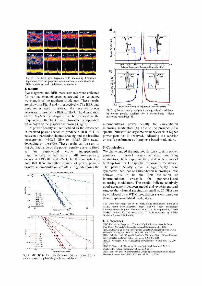
Fig 4: MZI BERs for channels above (a) and below (b) the resonance wavelength of the graphene modulator
Fig 3: The MZI eye diagrams with increasing frequency separation from the graphene modulator’s resonance shown at 1 GHz modulation and 1.5 dBm received power.
Fig 5: a) Power penalty analysis for the graphene modulator. b) Power penalty analysis for a carrier-based silicon microring modulator [6].
4. Results Eye diagrams and BER measurements were collected for various channel spacings around the resonance wavelength of the graphene modulator. These results are shown in Fig. 3 and 4, respectively. The BER data trendline is used to extract the received power necessary to produce a BER of 1E-9. The degradation of the MZM’s eye diagram can be observed as the frequency of the light moves towards the operation wavelength of the graphene microring (Fig. 3).
A power penalty is then defined as the difference in received power needed to produce a BER of 1E-9 between a particular channel spacing and the baseline measurement (+102.5 GHz or –102.5 GHz away, depending on the side). These results can be seen in Fig 5a. Each side of the power penalty curve is fitted to an exponential curve independently. Experimentally, we find that a 0.1 dB power penalty occurs at +19 GHz and –24 GHz. It is important to note that there are other sources of power penalty besides intermodulation crosstalk. Fig. 5b shows the
intermodulation power penalty for carrier-based microring modulators [6]. Due to the presence of a spectral blueshift, an asymmetric behavior with higher power penalties is observed, indicating the superior crosstalk performance of graphene-based modulators.
5. Conclusions We characterized the intermodulation crosstalk power penalties of novel graphene-enabled microring modulators, both experimentally and with a model built up from the DC spectral response of the device. The power penalty curve is significantly more symmetric than that of carrier-based microrings. We believe this to be the first evaluation of intermodulation crosstalk for graphene-based microring modulators. The results indicate relatively good agreement between model and experiment, and suggest that channel spacings as small as 25 GHz can be employed by a WDM modulation system based on these graphene-enabled modulators. This work was supported by an Early Stage Innovations grant (ESI NASA Grant NNX16AD16G) from NASA’s Space Technology Research Grants Program. The work of N. C. A. is supported by a DoD NDSEG Fellowship. The work of C. T. P. is supported by a NSF Graduate Research Fellowship
6. References [1] C. Kachris, K. Bergman, I. Tomkos, “Optical Interconnects for Future Data Center Networks”, Spring Science and Business Media, 2012 [2] K. Padmaraju et. al. “Intermodulation Crosstalk Characteristics of WDM Silicon Microring Modulators”, IEEE PTL, Vol. 26, No. 14, 2014. [3] M. Bahadori et al. “Crosstalk Penalty in Microring-Based Silicon Photonic Interconnected Systems”, IEEE JLT, Vol. 34, No. 17, 2016 [4] K. S. Novoselov et al. “A Roadmap for Graphene”, Nature 490, 192-200 (2012) [5] C. T. Phare et al. “Graphene Electro-Optic Modulator with 30 GHz Bandwidth”, Nature Photonics, Vol. 9, No. 8, 2015 [6] M. Bahadori et al. “Comprehensive Design Space Exploration of Silicon Photonic Interconnects”, IEEE JLT, Vol. 34, No. 12, 2016