Embed Size (px)
Citation preview
advanced aerospace rf, pcb & pcba technology delivered in two weeKs
case study
a tier one oeM developed ahighly complex pcba using
Mpar technology fordefense and aerospace
applications. the pcb andpcba technology were
highly complex, makingthe product almostunmanufacturable.
sanmina’s uniquecombination of advanced
pcb, pcba and testengineering expertise
enabled delivery of the firstpcba’s in two weeks and 70 assemblies in two months.
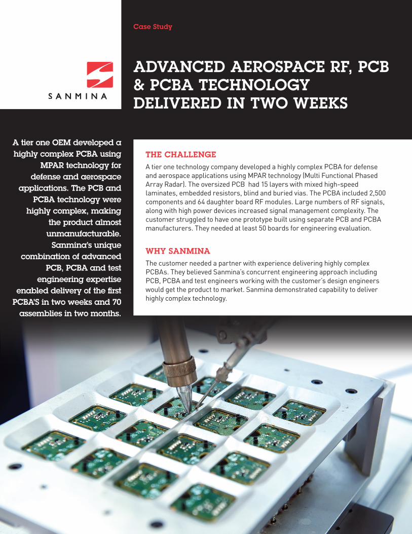
the challengeA tier one technology company developed a highly complex PCBA for defense and aerospace applications using MPAR technology (Multi Functional Phased Array Radar). The oversized PCB had 15 layers with mixed high-speed laminates, embedded resistors, blind and buried vias. The PCBA included 2,500 components and 64 daughter board RF modules. Large numbers of RF signals, along with high power devices increased signal management complexity. The customer struggled to have one prototype built using separate PCB and PCBA manufacturers. They needed at least 50 boards for engineering evaluation.
why sanMinaThe customer needed a partner with experience delivering highly complex PCBAs. They believed Sanmina’s concurrent engineering approach including PCB, PCBA and test engineers working with the customer’s design engineers would get the product to market. Sanmina demonstrated capability to deliver highly complex technology.
CS01_CT_071317
©2017 Sanmina Corporation. Sanmina is a trademark or registered trademark in the U.S. and/or other jurisdictions of Sanmina Corporation. All trademarks and registered trademarks are the property of their respective owners.
About SAnminASanmina makes some of the most complex and innovative optical, electronic and mechanical products in the world. Recognized as a technology leader, Sanmina provides end-to-end design, manufacturing and logistics solutions, delivering superior quality and support to Original Equipment Manufacturers (OEMs) primarily in the communications networks, computing and storage, medical, defense and aerospace, industrial and semiconductor, multimedia, automotive and clean technology sectors.
More information regarding the company is available at www.sanmina.com
.
sanMina’s approach• SanminaPCBengineersrecommendedaspecificmixoflaminatestoshieldandisolatevariousRFsignals.
• They tested three materials to develop the best recommendation for rohasol bonding.
• A multi-stage PCB manufacturing process was developed building 4 layers at a time, incorporating complex buried and blind via structures.
• Controlled depth milling was used to accommodate the 64 RF modules.
• Cavities were milled out in the mother board to shield the RF modules from interference.
• Sanmina test engineers worked in collaboration with the customer’s design engineers to provide test access while minimizing RF interference.
• 5DX x-ray was used to inspect non-visible elements of the PCBA.
• ExperimentswereconductedwiththermocouplesattachedtothePCBAtodeveloptheoptimumreflowprofileforhigher reliability.
• A unique rework process was developed for this advanced PCBA.
results• ThefirstworkingPCBAwasproducedwithintwoweeks.
• 70 pre-production PCBAs were manufactured within 4 months.
• A consistent approach to manufacturing the PCB was developed.