Embed Size (px)
DESCRIPTION
High voltage planar transformer is a technology which can replace conventional transformer with its distinct advantages of saturation and cost efficiency. This paper includes, study and solution methods for PCB winding configuration in planar magnetic elements with multilayer stack up of PCB Cu-tracks, producing High voltage power supply for aerospace application.With finite element analysis (FEA) simulations, different simulation outcomes are discussed for inspecting flux intensity and current density distribution with computing Electric field strength and Magnetic fields. In principal conclusion of study, complete analysis and some practical design guidelines for multilayer PCB stack up are discussed in this paper.
Citation preview
Electrical and Electronics Engineering: An International Journal (ELELIJ) Vol 3, No 4, November 2014
DOI : 10.14810/elelij.2014.3402 11
FEA OF PCB MULTILAYER STACK UP
HIGH VOLTAGE PLANAR TRANSFORMER
FOR AEROSPACE APPLICATION
Kiran Gaikwad1; Tobias Bartusch
2
1Analytical Instrument, Measurement and Sensor technology,
Hochschule Coburg, Germany [email protected]
2Airbus Defence and Space, Ottobrunn, Germany
ABSTRACT
High voltage planar transformer is a technology which can replace conventional transformer
with its distinct advantages of saturation and cost efficiency. This paper includes, study and
solution methods for PCB winding configuration in planar magnetic elements with multilayer
stack up of PCB Cu-tracks, producing High voltage power supply for aerospace application.
With finite element analysis (FEA) simulations, different simulation outcomes are discussed for
inspecting flux intensity and current density distribution with computing Electric field strength
and Magnetic fields.
In principal conclusion of study, complete analysis and some practical design guidelines for
multilayer PCB stack up are discussed in this paper.
KEYWORDS
Planar transformer, PCB tracks, FEA.
1. INTRODUCTION
In recent years, industries such as military/aerospace, hybrid vehicles, and alternative energy are
benefiting from planar technology that features high performance from a low-profile design
package and are ideal for applications where the space, weight and cost are vital. This printed
circuit replaces typically wire wound coils to flat, extremely durable, high temperature resilient,
high inner layer, and voltage dielectric breakdown rating PCB tracks. Planar magnetics refer to
high-frequency transformers and inductors exhibiting advantages in electrical, thermal and
mechanical aspects [1].
With Planar technology, instead of constructing magnetics components as transformer and
inductors of wire-wound assemblies on bobbin, the planar PCB magnetics take benefits from
using PCB-tracks as windings. Main advantages are the simplification of assembly and no longer
requirement of the magnetics screening tests. This is a part of the implemented cost reduction
Electrical and Electronics Engineering: An International Journal (ELELIJ) Vol 3, No 4, November 2014
12
measures. Even layers with one and two layers are common. So it is also used in low voltage high
current applications.
This paper presents optimized planar transformer solutions for aerospace application with low
profile, EMI and low costs. It gives detailed studies influence of magnetic field distribution and
eddy currents effects due to windings arrangements inside multilayer stack up. A finite element
analysis simulation gives detailed calculation of field intensity and current density distribution of
planar for aerospace application. Finally some design aspects and conclusions are discussed in
this paper with necessary design guidelines.
2. HIGH VOLTAGE APPLICATION
High Power Amplifier (HPA) is needed in the satellite communication to operate transmission
amplifiers. To supply electronics power, Electronic Power Conditioner (EPC) is used in addition
to tube with the necessary operating voltages. It acts as a High Power Amplifier when connected
together with a Klystron. The klystron is a vacuum tube that takes advantage of runtime of
electrons to creation or reinforcement of high-frequency signals, while the disadvantage is heavy
weight and large size power supply. Also a core equipment of an Ion Thruster Unit is the High
Voltage Power Supply (HVPS), which is dedicated to condition the electrical power from the
spacecraft main bus. Key issue of this power equipment is the generation of high voltage in the
range of 1.2 kV for Kaufmann-Type and RIT-Type ion engines and up to 13 kV for Field
Emission Type thrusters [2] [3]. Thus planar magnetics were considered for its power supply
which was challenging part for high voltage of 10-12 KV.
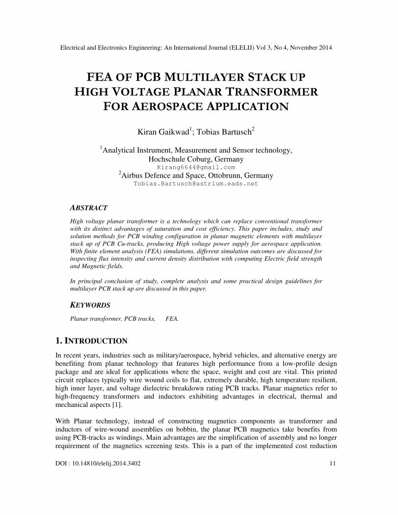
Figure below gives schematic for transformer section of HVPS power supply. Planar transformer
plays an important role in this power supply. It has one primary winding and three secondary
windings.
Figure 1. Schematic of Planar for high voltage application
Electrical and Electronics Engineering: An International Journal (ELELIJ) Vol 3, No 4, November 2014
13
In electrical power transformer, there are primary, secondary and may be tertiary windings.
Performance of a transformer mainly depends upon the flux linkages between these windings. For
efficient flux linking between these windings, one low reluctance magnetic path common to all
windings should be provided in the transformer. This low reluctance magnetic path in transformer
is known as core of transformer. So selecting proper transformer core is one of the important and
crucial parts in design of transformer.
After tradeoffs and market survey we concluded to select ferrite core for planar transformer
importantly due to its high saturation and dimensions. This ferrite core by Magnetics®
OR49938EC is of size 10 x 20.3 x 37.5 mm, pair of E cores and manufactured from P&R grade
material. This material type is a low to medium frequency power material with minimum core
losses at 100 kHz, 100mT and 100° C for use of power transformers up to 500 kHz [4]. This core
has high permeability and low losses at high flux densities and temperatures. Also it has high
saturation and low existing currents [5].
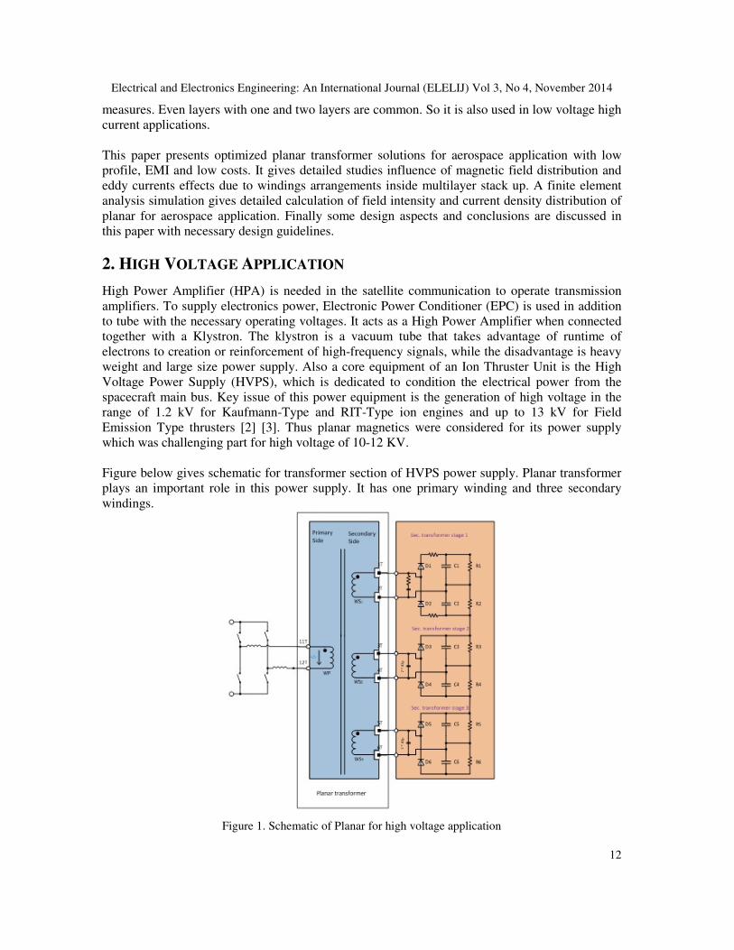
Figure 2 shows the winding arrangement of high voltage planar transformer. Primary windings
has two turns (WP= 2) and the secondary has 96 turns (WS1=WS2=WS3= 96).
Figure 2. Winding arrangement of high voltage transformer
Figure shows PCB stack up implemented in E-Core. Details of boundary/sources are mention
below.
- Total no of PCB stack-up : 3
- Primary no of turns NPRI : 2
- Secondary no of turns NSEC : 288
(Per layer: 24; one stack-up: 96)
- Primary Voltage : 51 V
- Secondary voltages :
WS1: 0-3270 volt
Total windings: 96; distributed voltage is ∆U 34.5 volt per winding.
WS2: 3300-6770 volt
Total windings: 96; distributed voltage is ∆U 36.5 volt per winding.
WS3: 6800-10360 volt
Total windings: 96; distributed voltage is ∆U 37.5 volt per winding.
Electrical and Electronics Engineering: An International Journal (ELELIJ) Vol 3, No 4, November 2014
14
3. STACK UP DESIGN
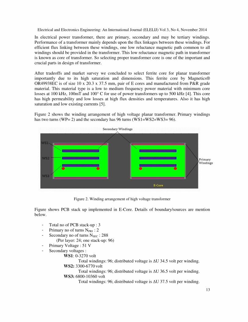
Figure 3 shows one layer of PCB stack up design from secondary windings, which includes PCB
tracks of 0.06mm, same size feedback and these layers are separated with FR4-epoxy core of
0.25mm. Feedback layer is used because of large voltage difference i.e. around 500 Volts
between each layer, which increases losses and high electric field around windings.
Implementation of this feedback layer reduces these effects. Highlighted area in Figure 3 shows
single PCB track winding with its mechanical dimensions.
Width: 0.7 mm (down)
Width: 0.6 mm (up): (Size considered after effect of etching process)
Height: 0.06 mm
Figure 3. Single layer dimensional description
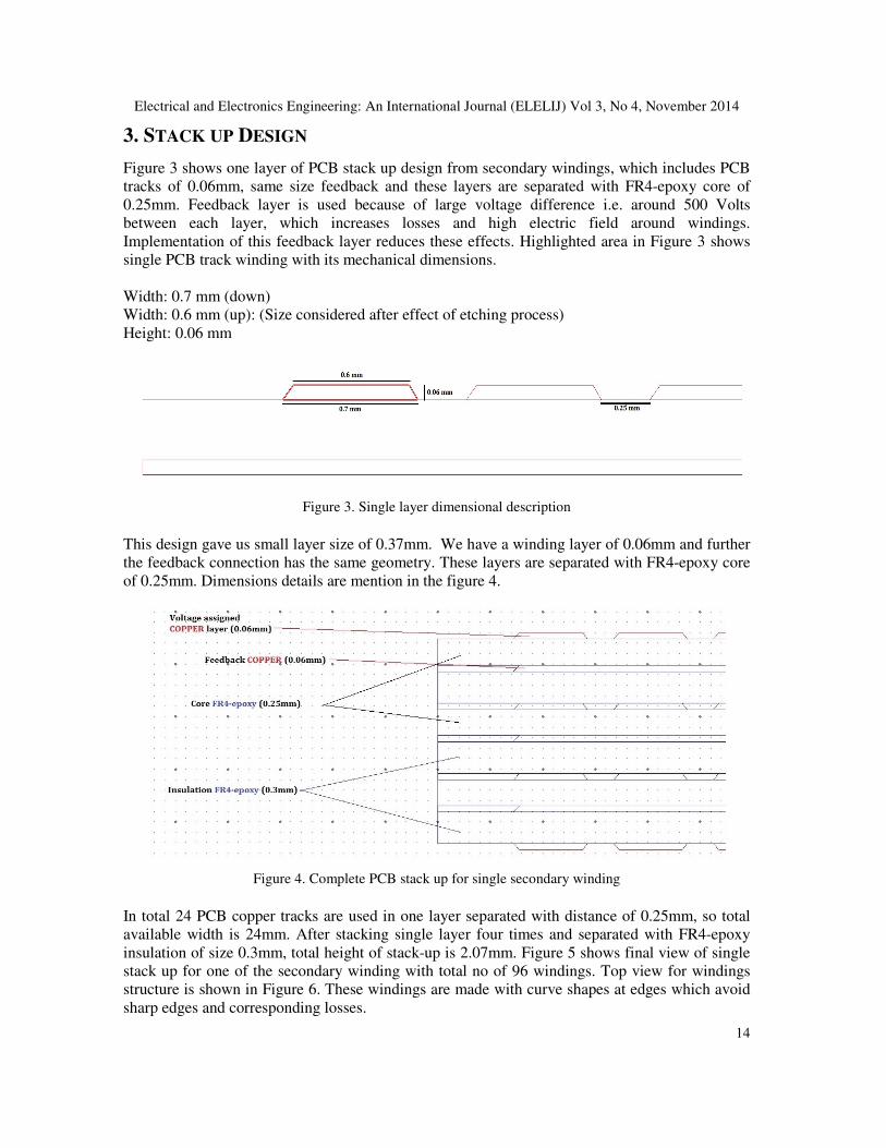
This design gave us small layer size of 0.37mm. We have a winding layer of 0.06mm and further
the feedback connection has the same geometry. These layers are separated with FR4-epoxy core
of 0.25mm. Dimensions details are mention in the figure 4.
Figure 4. Complete PCB stack up for single secondary winding
In total 24 PCB copper tracks are used in one layer separated with distance of 0.25mm, so total
available width is 24mm. After stacking single layer four times and separated with FR4-epoxy
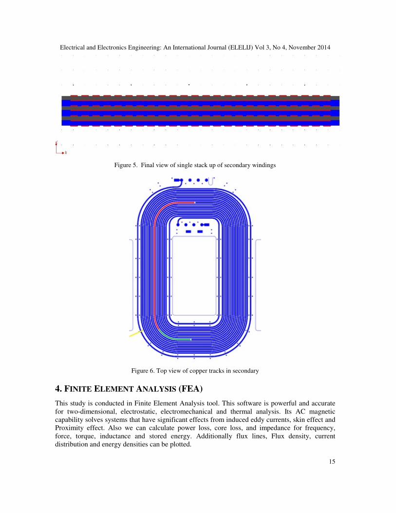
insulation of size 0.3mm, total height of stack-up is 2.07mm. Figure 5 shows final view of single
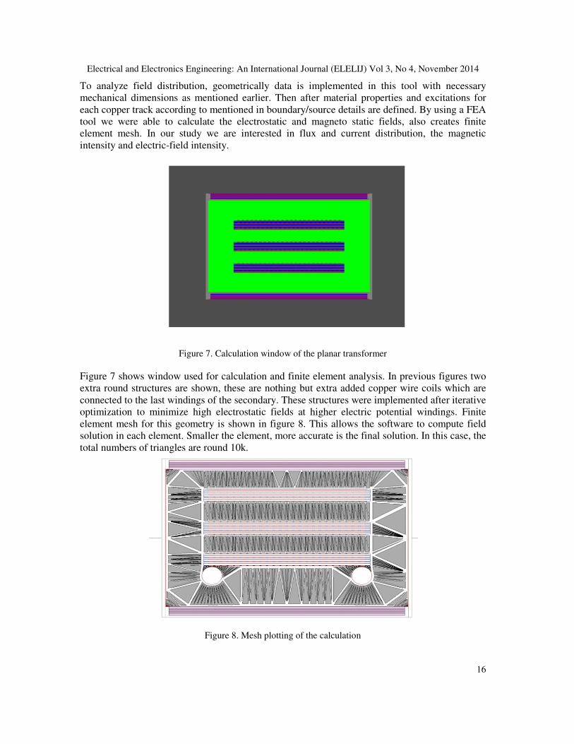
stack up for one of the secondary winding with total no of 96 windings. Top view for windings
structure is shown in Figure 6. These windings are made with curve shapes at edges which avoid
sharp edges and corresponding losses.
Electrical and Electronics Engineering: An International Journal (ELELIJ) Vol 3, No 4, November 2014
15
Figure 5. Final view of single stack up of secondary windings
Figure 6. Top view of copper tracks in secondary
4. FINITE ELEMENT ANALYSIS (FEA)
This study is conducted in Finite Element Analysis tool. This software is powerful and accurate
for two-dimensional, electrostatic, electromechanical and thermal analysis. Its AC magnetic
capability solves systems that have significant effects from induced eddy currents, skin effect and
Proximity effect. Also we can calculate power loss, core loss, and impedance for frequency,
force, torque, inductance and stored energy. Additionally flux lines, Flux density, current
distribution and energy densities can be plotted.
Electrical and Electronics Engineering: An International Journal (ELELIJ) Vol 3, No 4, November 2014
16
To analyze field distribution, geometrically data is implemented in this tool with necessary
mechanical dimensions as mentioned earlier. Then after material properties and excitations for
each copper track according to mentioned in boundary/source details are defined. By using a FEA
tool we were able to calculate the electrostatic and magneto static fields, also creates finite
element mesh. In our study we are interested in flux and current distribution, the magnetic
intensity and electric-field intensity.
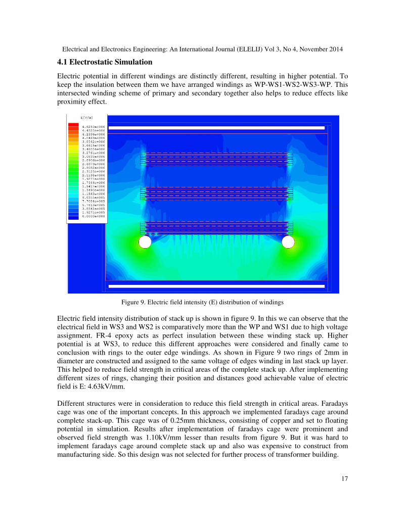
Figure 7. Calculation window of the planar transformer
Figure 7 shows window used for calculation and finite element analysis. In previous figures two
extra round structures are shown, these are nothing but extra added copper wire coils which are
connected to the last windings of the secondary. These structures were implemented after iterative
optimization to minimize high electrostatic fields at higher electric potential windings. Finite
element mesh for this geometry is shown in figure 8. This allows the software to compute field
solution in each element. Smaller the element, more accurate is the final solution. In this case, the
total numbers of triangles are round 10k.
Figure 8. Mesh plotting of the calculation
Electrical and Electronics Engineering: An International Journal (ELELIJ) Vol 3, No 4, November 2014
17
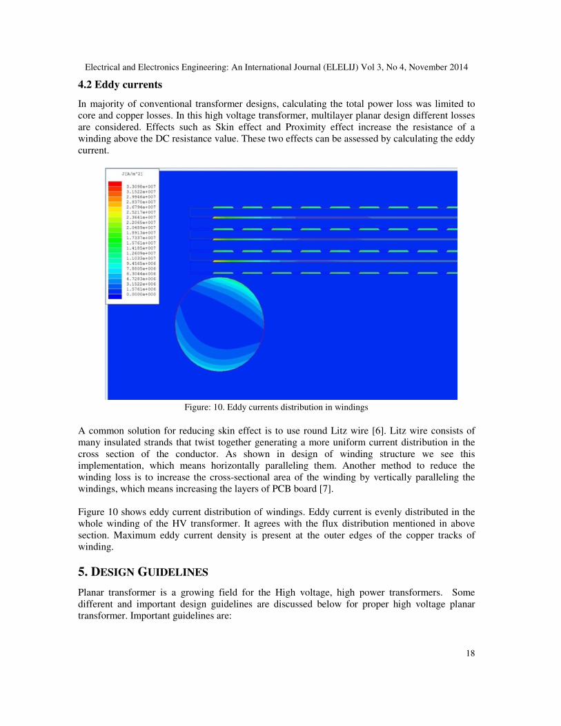
4.1 Electrostatic Simulation
Electric potential in different windings are distinctly different, resulting in higher potential. To
keep the insulation between them we have arranged windings as WP-WS1-WS2-WS3-WP. This
intersected winding scheme of primary and secondary together also helps to reduce effects like
proximity effect.
Figure 9. Electric field intensity (E) distribution of windings
Electric field intensity distribution of stack up is shown in figure 9. In this we can observe that the
electrical field in WS3 and WS2 is comparatively more than the WP and WS1 due to high voltage
assignment. FR-4 epoxy acts as perfect insulation between these winding stack up. Higher
potential is at WS3, to reduce this different approaches were considered and finally came to
conclusion with rings to the outer edge windings. As shown in Figure 9 two rings of 2mm in
diameter are constructed and assigned to the same voltage of edges winding in last stack up layer.
This helped to reduce field strength in critical areas of the complete stack up. After implementing
different sizes of rings, changing their position and distances good achievable value of electric
field is E: 4.63kV/mm.
Different structures were in consideration to reduce this field strength in critical areas. Faradays
cage was one of the important concepts. In this approach we implemented faradays cage around
complete stack-up. This cage was of 0.25mm thickness, consisting of copper and set to floating
potential in simulation. Results after implementation of faradays cage were prominent and
observed field strength was 1.10kV/mm lesser than results from figure 9. But it was hard to
implement faradays cage around complete stack up and also was expensive to construct from
manufacturing side. So this design was not selected for further process of transformer building.
Electrical and Electronics Engineering: An International Journal (ELELIJ) Vol 3, No 4, November 2014
18
4.2 Eddy currents
In majority of conventional transformer designs, calculating the total power loss was limited to
core and copper losses. In this high voltage transformer, multilayer planar design different losses
are considered. Effects such as Skin effect and Proximity effect increase the resistance of a
winding above the DC resistance value. These two effects can be assessed by calculating the eddy
current.
Figure: 10. Eddy currents distribution in windings
A common solution for reducing skin effect is to use round Litz wire [6]. Litz wire consists of
many insulated strands that twist together generating a more uniform current distribution in the
cross section of the conductor. As shown in design of winding structure we see this
implementation, which means horizontally paralleling them. Another method to reduce the
winding loss is to increase the cross-sectional area of the winding by vertically paralleling the
windings, which means increasing the layers of PCB board [7].
Figure 10 shows eddy current distribution of windings. Eddy current is evenly distributed in the
whole winding of the HV transformer. It agrees with the flux distribution mentioned in above
section. Maximum eddy current density is present at the outer edges of the copper tracks of
winding.
5. DESIGN GUIDELINES
Planar transformer is a growing field for the High voltage, high power transformers. Some
different and important design guidelines are discussed below for proper high voltage planar
transformer. Important guidelines are:
Electrical and Electronics Engineering: An International Journal (ELELIJ) Vol 3, No 4, November 2014
19
• Secondary side windings are to be arranged according to the increase in voltage.
• It is better to implement intersected winding scheme of primary and secondary windings,
together which helps to avoid effect as proximity effect.
• Proper shielding to be implemented in order to avoid high electric field in the windings.
Sharp edges which are exposed to electrical field shall be avoided.
• Implementation of copper feedback track layer between two layers of voltage assignment.
• Proper insulation to be considered in different layers of stack up and between different
windings of the secondary section to avoid voltage breakdown.
• Take the eddy current effect into account, the outer PCB track may be a little broader
than the inner in order to reduce the AC resistance.
6. CONCLUSION
Planar magnetics is growing in the field of high voltage, high power transformer with large scope
of application. Due to their higher reliability, better reproducibility and lower costs now are
considerable option in aerospace application. Overall calculation results shows that it is possible
to consider planar transformer with PCB tracks for high voltage high power aerospace
application.
REFERENCES
[1] Quirke, M.T.; Barrett, J.J.; Hayes, M., "Planar magnetic component technology-a
review,"Components, Hybrids, and Manufacturing Technology, IEEE Transactions on, vol.15, no.5,
pp.884-892, Oct 1992
[2] Frank, H.; Franke, A.; Kiewe, B., "Single-stage high voltage power supply for ion engines", 8th
European Space Power Conference, Constance, Germany, 14–19 September 2008
[3] Michael, B.; Frank, H.; Kurt, R.; Matthias, G., "Generic high voltage power module for electrical
propulsion", 29th
International electrical propulsion conference, Princeton university. Oct 31- Nov 4
2005
[4] Document OR49938EC Datasheet: OR49938EC Magnetics® planar E core.
[5] www.mag-inc.com
[6] Shen Wang; de Rooij, M.A.; Odendaal, W.G.; van Wyk, J.D.; Boroyevich, D., "Reduction of high-
frequency conduction losses using a planar litz structure," Power Electronics, IEEE Transactions on,
vol.20, no.2, pp. 261-267, March 2005
[7] Wei Chen; Yipeng Yan; Yuequan Hu; Qing Lu, "Model and design of PCB parallel winding for
planar transformer," Magnetics, IEEE Transactions on , vol.39, no.5, pp. 3202-3204, Sept. 2003
AUTHORS
Kiran Gaikwad completed his Diploma and Bachelors in Electronics and
Telecommunication engineering from university of Pune, India in year 2008 and
2011 respectively. Currently he is pursuing M.Eng in Analytical instrument,
Measurements and Sensor technology from Hochschule Coburg (Coburg
university of applied science), Coburg, Germany, in corporation with University
of Shanghai for science and Technology (USST) Shanghai, China. from
september 2012.
Electrical and Electronics Engineering: An International Journal (ELELIJ) Vol 3, No 4, November 2014
20
He was research assistant in Rössel messtechnik and summer intern in Airbus Defence and Space in
electronic department for Space during Nov 2013- Jul 2014. He is currently doing his master thesis with
Anode current measurement unit (ACMU) in Secondary power source of Electronic department Airbus
Defence and Space, Friedrichshafen, Germany.
Tobias Bartusch is an expert with a Diploma in Telecommunications Electronic
Engineering and Solid State Experimental Physics. His expertise is mainly in the
fields of analog electronics, low noise circuits, vacuum electronics, RF systems,
EMC, high voltage systems, electrical propulsion and plasma physics. In the
years 2003 - 2008 he invented and developed a electrodeless plasma thruster and
some applications for RF high voltage plasma and plasma cutting systems. Since
end of 2008, he is at Airbus Defence and Space. He developed parts of the
Galileo CMCU and actually, he is Systems Engineer for the IRNSS Atomic clock
monitoring unit (ACMU) / RAFS project. Additionally he is a co engineer for the
study of the high voltage planar transformer.