Embed Size (px)
Citation preview

ADS1298ECG-FE/ADS1198ECG-FEECG Front-End Performance Demonstration Kit
User's Guide
Literature Number: SBAU171C
May 2010–Revised September 2012
Contents
1 ADS1298ECG-FE/ADS1198ECG-FE Overview ......................................................................... 71.1 Important Disclaimer Information ...................................................................................... 7
1.2 Introduction ............................................................................................................... 8
1.3 Supported Features ..................................................................................................... 8
1.4 Features Not Supported in Current Version ......................................................................... 8
1.5 ADS1x98ECG-FE Hardware ........................................................................................... 8
1.6 Minimum System Requirements for ADS1x98ECG-FE Evaluation Software ................................... 9
2 Quick Start ....................................................................................................................... 102.1 Default Jumper/Switch Configuration ............................................................................... 10
2.2 ADS1x98ECG-FE Operation ......................................................................................... 11
3 Using the ADS1298ECG-FE Software ................................................................................... 123.1 Application User Menu ................................................................................................ 13
3.2 Top-Level Application Controls ....................................................................................... 13
3.3 About Tab ............................................................................................................... 14
3.4 ADC Register Tab ..................................................................................................... 15
3.5 Analysis Tab ............................................................................................................ 23
3.6 Save Tab ................................................................................................................ 31
4 ADS1x98ECG-FE Input Signals ........................................................................................... 334.1 Input Short Testing .................................................................................................... 33
4.2 Internal Test Signals Input ............................................................................................ 33
4.3 Temperature Sensor ................................................................................................... 34
4.4 Normal Electrode Input ................................................................................................ 35
4.5 MVDD Input, RLD Measurement, RLD Positive Electrode Driver, and RLD Negative Electrode Driver ..... 35
4.6 Lead Derivation ........................................................................................................ 36
4.7 Wilson Center Terminal (WCT) ...................................................................................... 36
4.8 Right Leg Drive ......................................................................................................... 36
4.9 PACE Detection ........................................................................................................ 37
5 ADS1298ECG-FE/ADS1198ECG-FE Hardware Details ............................................................. 395.1 Jumper Description .................................................................................................... 40
5.2 Power Supply ........................................................................................................... 41
5.3 Clock ..................................................................................................................... 42
5.4 Reference ............................................................................................................... 42
5.5 Analog Output Signals ................................................................................................ 43
5.6 Digital Signals .......................................................................................................... 43
5.7 Analog Input Signals .................................................................................................. 43
Appendix A Schematics, BOM, Layout, and ECG Cable Details ....................................................... 45A.1 ADS1x98ECG-FE Front-End Board Schematics ................................................................. 45
A.2 Bill of Materials ........................................................................................................ 46
A.3 Printed Circuit Board Layout ........................................................................................ 48
A.4 ECG Cable Details ................................................................................................... 50
Appendix B External Optional Hardware ...................................................................................... 51
2 Table of Contents SBAU171C–May 2010–Revised September 2012Submit Documentation Feedback
Copyright © 2010–2012, Texas Instruments Incorporated
www.ti.com
B.1 Optional External Hardware (Not Included) ....................................................................... 51
B.2 ADS1x98ECG-FE Power-Supply Recommendations ............................................................ 53
Appendix C Software Installation ................................................................................................. 54C.1 Minimum Requirements ............................................................................................. 54
C.2 Installing the Software ............................................................................................... 54
3SBAU171C–May 2010–Revised September 2012 ContentsSubmit Documentation Feedback
Copyright © 2010–2012, Texas Instruments Incorporated
www.ti.com
List of Figures
1 ADS1x98ECG-FE Kit ....................................................................................................... 9
2 ADS1x98ECG-FE Default Jumper Locations .......................................................................... 10
3 Software Start Screen/About Tab ....................................................................................... 12
4 User Menu - File Item..................................................................................................... 13
5 User Menu - Help Item.................................................................................................... 13
6 Top Level Controls ........................................................................................................ 13
7 Lead-Off Status Registers Display Window............................................................................ 14
8 Channel Registers Tab ................................................................................................... 15
9 Internal Reference and Buffer Connections............................................................................ 16
10 Lead-Off Excitation Options .............................................................................................. 17
11 Input Multiplexer for a Single Channel.................................................................................. 17
12 LOFF and RLD Tab ....................................................................................................... 18
13 LOFF_STATP and LOFF_STATN Comparators ...................................................................... 19
14 GPIO and OTHER Register Tab ........................................................................................ 20
15 Wilson Central and Augmented Lead Routing Diagrams ............................................................ 21
16 Device Registers Settings ................................................................................................ 22
17 Scope Tool Features...................................................................................................... 23
18 Scope Analysis Tab (Noise Levels for Each Channel Shown) ...................................................... 23
19 Zoom Tool Options ........................................................................................................ 24
20 Histogram Bins for 12-Lead ECG Signal ............................................................................... 25
21 Statistics for the Signal Amplitude of Eight ECG Channels.......................................................... 25
22 FFT Graph of Normal Electrode Configuration ........................................................................ 26
23 AC Analysis Parameters: Windowing Options......................................................................... 26
24 FFT Analysis: Input Short Condition .................................................................................... 27
25 Changing the User-Defined Dynamic Range for Channel 1 ......................................................... 27
26 FFT Plot Using Zoom Tool ............................................................................................... 28
27 ECG Display Tab Showing LEAD I-III and Augmented Leads ...................................................... 29
28 ECG Signal Zoom Feature for Six Leads .............................................................................. 30
29 ECG Signal Zoom Feature for Lead 1 .................................................................................. 30
30 Save Tab ................................................................................................................... 32
31 Example of Internal Test Signals Viewed on the ECG Display Tab ................................................ 33
32 Internal Temperature Sensor ............................................................................................ 34
33 Eight-Channel Read of Internal Temperature ......................................................................... 34
34 Normal Electrode ECG Connection in ECG Display Tab ............................................................ 35
35 Digitization of PACE Signal Using ADS1298 .......................................................................... 38
36 ADS1298ECG-FE Front-End Block Diagram .......................................................................... 39
37 Fluke Simulator Configuration ........................................................................................... 44
38 Top Component Placement .............................................................................................. 48
39 Top Layer................................................................................................................... 48
40 Bottom Component Placement .......................................................................................... 48
41 Bottom Layer ............................................................................................................... 48
42 Internal Ground Plane (Layer 2)......................................................................................... 48
43 Internal Power Plane (Layer 3) .......................................................................................... 48
44 ECG Cable Schematic .................................................................................................... 50
45 15-Pin, Shielded Connector from Biometric Cables .................................................................. 51
46 15-Pin, Twisted Wire Cable to Banana Jacks ......................................................................... 51
47 15-Pin, Twisted Wire Cable .............................................................................................. 51
4 List of Figures SBAU171C–May 2010–Revised September 2012Submit Documentation Feedback
Copyright © 2010–2012, Texas Instruments Incorporated
www.ti.com
48 Cardiosim ECG Simulator Tool .......................................................................................... 52
49 Recommended Power Supply for ADS1x98ECG-FE................................................................. 53
50 Initialization of ADS1x98ECG-FE ....................................................................................... 54
51 License Agreement........................................................................................................ 54
52 Installation Process........................................................................................................ 55
53 Completion of ADS1x98ECG-FE Software Installation............................................................... 55
5SBAU171C–May 2010–Revised September 2012 List of FiguresSubmit Documentation Feedback
Copyright © 2010–2012, Texas Instruments Incorporated
www.ti.com
List of Tables
1 ADS1x98ECG-FE Default Jumper/Switch Configuration............................................................. 11
2 ADS1298 Lead Measurements .......................................................................................... 36
3 Derived Lead Calculations ............................................................................................... 36
4 RLD Jumper Options...................................................................................................... 37
5 ADS1x98ECG-FE Default Jumper/Switch Configuration............................................................. 40
6 Power-Supply Test Points................................................................................................ 41
7 Analog Supply Configurations (AVDD/AVSS) ......................................................................... 42
8 Digital Supply Configurations (DVDD/DGND) ......................................................................... 42
9 CLK Jumper Options...................................................................................................... 42
10 External Reference Jumper Options .................................................................................... 43
11 Test Signals ................................................................................................................ 43
12 Serial Interface Pinout .................................................................................................... 43
13 Bill of Materials: ADS1x98ECG-FE ..................................................................................... 46
6 List of Tables SBAU171C–May 2010–Revised September 2012Submit Documentation Feedback
Copyright © 2010–2012, Texas Instruments Incorporated
User's GuideSBAU171C–May 2010–Revised September 2012
ADS1298ECG-FE/ADS1198ECG-FE
This user's guide describes the characteristics, operation, and use of the ADS1298ECG-FE andADS1198ECG-FE. The ADS1298ECG-FE and ADS1198ECG-FE are evaluation modules for theADS1298, an eight-channel, 24-bit, and ADS1198, an eight-channel, 16-bit, analog-to digital converter(ADC). Both devices provide low-power, integrated analog front-end (AFE) designs for patient monitoringand portable and high-end electrocardiogram (ECG) and electroencephalogram (EEG) applications. Thisuser's guide includes a complete circuit description, schematic diagram, and bill of materials.
The following related documents are available through the Texas Instruments web site at www.ti.com.
Device Literature Number
ADS1298 SBAS459
ADS1198 SBAS471
1 ADS1298ECG-FE/ADS1198ECG-FE Overview
1.1 Important Disclaimer Information
CAUTION
NOTICE: The ADS1298ECG-FE and ADS1198ECG-FE are intended forfeasibility and evaluation testing only in laboratory and developmentenvironments. This product is not for diagnostic use. This product is not for usewith a defibrillator.
The ADS1298ECG-FE/ADS1198ECG-FE is to be used only under these conditions:
• The ADS1298ECG-FE/ADS1198ECG-FE is intended only for electrical evaluation of the features ofthe ADS1298 device in a laboratory, simulation, or development environment.
• The ADS1298ECG-FE/ADS1198ECG-FE is not intended for direct interface with a patient, patientdiagnostics, or with a defibrillator.
• The ADS1298ECG-FE/ADS1198ECG-FE is intended for development purposes ONLY. It is notintended to be used as all or part of an end equipment application.
• The ADS1298ECG-FE/ADS1198ECG-FE should be used only by qualified engineers and technicianswho are familiar with the risks associated with handling electrical and mechanical components,systems, and subsystems.
• The user is responsible for the safety of themselves, fellow employees and contractors, and co-workers when using or handling the ADS1298ECG-FE/ADS1198ECG-FE. Furthermore, the user isfully responsible for the contact interface between the human body and electronics; consequently, theuser is responsible for preventing electrical hazards such as shock, electrostatic discharge, andelectrical overstress of electric circuit components.
Pentium III, Celeron are registered trademarks of Intel Corporation.Microsoft, Windows are registered trademarks of Microsoft Corporation.SPI is a trademark of Motorola Inc.All other trademarks are the property of their respective owners.
7SBAU171C–May 2010–Revised September 2012 ADS1298ECG-FE/ADS1198ECG-FESubmit Documentation Feedback
Copyright © 2010–2012, Texas Instruments Incorporated

ADS1298ECG-FE/ADS1198ECG-FE Overview www.ti.com
1.2 Introduction
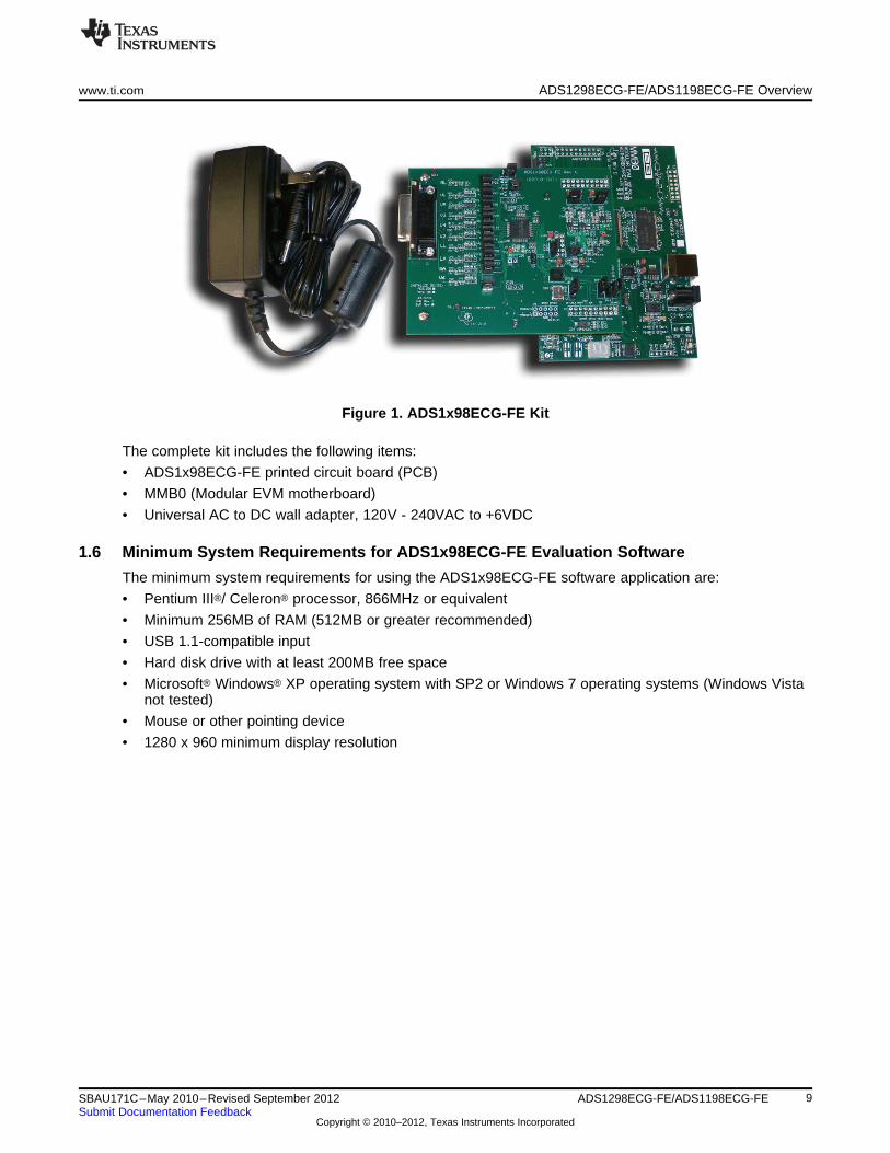
The ADS1x98ECG-FE is intended for evaluating the ADS1298 and ADS1198 for ECG and EEGapplications. The digital SPI™ control interface is provided by the MMB0 Modular EVM motherboard thatconnects to the ADS1x98ECG FE evaluation board. The ADS1x98ECG-FE (see Figure 1) is NOT areference design for ECG and EEG applications; rather, its purpose is to expedite evaluation and systemdevelopment. The output of the ADS1298 yields a raw, unfiltered ECG signal.
The MMB0 motherboard allows the ADS1x98 to be connected to the computer via an available USB port.This manual shows how to use the MMB0 as part of the ADS1x98ECG-FE, but does not provide technicaldetails about the MMB0 itself.
This document covers the operation of the ADS1x98ECG-FE evaluation system. Throughout thedocument, the abbreviation EVM and the term evaluation module are synonymous with theADS1x98ECG-FE . For clarity of reading, this manual will refer only to the ADS1298ECG-FE orADS1x98ECG-FE, but operation of the ADS1198ECG-FE is identical, unless otherwise noted.
CAUTION
Many of the components on the ADS1x98ECG-FE are susceptible to damageby electrostatic discharge (ESD). Customers are advised to observe properESD handling precautions when unpacking and handling the EVM, includingthe use of a grounded wrist strap, bootstraps, or mats at an approved ESDworkstation. An electrostatic smock and safety glasses should also be worn.
1.3 Supported Features
Hardware Features:• Configurable for bipolar or unipolar supply operation
• Configurable for internal and external clock and reference via jumper settings
• Configurable for AC- or DC-coupled inputs
• Configurable for up to 12 standard ECG leads
• External Right Leg Drive (RLD) Reference (VCC – VEE)/2
• External Wilson central voltage
• Easy connectivity to popular ECG simulators
Software Features:• Designed to display 12 lead ECG data
• Analysis tools including a virtual oscilloscope, histogram, FFT, and ECG display
• File printing for post-processing of raw ECG data
• Sets the ADS1298/ADS1198 register settings via easy-to-use graphic user interface (GUI) software
• Post-processing of ECG data using high-pass, low-pass, and 50/60Hz notch filters
1.4 Features Not Supported in Current Version• Real-time data processing
• AC lead-off detection filters
• QRS detection algorithms
• Software PACE detection algorithms
1.5 ADS1x98ECG-FE Hardware
Figure 1 shows the hardware included in the ADS1x98ECG-FE kit. Contact the factory if any component ismissing. The latest software is available for download on the TI website at http://www.ti.com.
8 ADS1298ECG-FE/ADS1198ECG-FE SBAU171C–May 2010–Revised September 2012Submit Documentation Feedback
Copyright © 2010–2012, Texas Instruments Incorporated
www.ti.com ADS1298ECG-FE/ADS1198ECG-FE Overview
Figure 1. ADS1x98ECG-FE Kit
The complete kit includes the following items:
• ADS1x98ECG-FE printed circuit board (PCB)
• MMB0 (Modular EVM motherboard)
• Universal AC to DC wall adapter, 120V - 240VAC to +6VDC
1.6 Minimum System Requirements for ADS1x98ECG-FE Evaluation Software
The minimum system requirements for using the ADS1x98ECG-FE software application are:
• Pentium III®/ Celeron® processor, 866MHz or equivalent
• Minimum 256MB of RAM (512MB or greater recommended)
• USB 1.1-compatible input
• Hard disk drive with at least 200MB free space
• Microsoft® Windows® XP operating system with SP2 or Windows 7 operating systems (Windows Vistanot tested)
• Mouse or other pointing device
• 1280 x 960 minimum display resolution
9SBAU171C–May 2010–Revised September 2012 ADS1298ECG-FE/ADS1198ECG-FESubmit Documentation Feedback
Copyright © 2010–2012, Texas Instruments Incorporated
Quick Start www.ti.com
2 Quick Start
This section provides a QuickStart guide to quickly begin evaluating the EVM using the ADS1x98ECG-FEsoftware.
2.1 Default Jumper/Switch Configuration
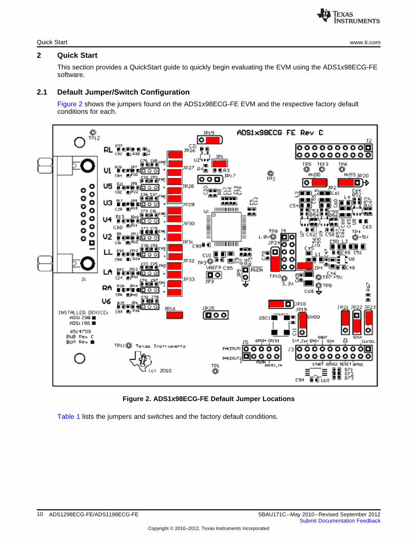
Figure 2 shows the jumpers found on the ADS1x98ECG-FE EVM and the respective factory defaultconditions for each.
Figure 2. ADS1x98ECG-FE Default Jumper Locations
Table 1 lists the jumpers and switches and the factory default conditions.
10 ADS1298ECG-FE/ADS1198ECG-FE SBAU171C–May 2010–Revised September 2012Submit Documentation Feedback
Copyright © 2010–2012, Texas Instruments Incorporated
www.ti.com Quick Start
Table 1. ADS1x98ECG-FE Default Jumper/Switch Configuration
Jumper Default Position Description
JP1 Installed RLD feedback
JP2 Installed 1-2 AVDD selected for bipolar supply operation selected (AVDD = +2.5V)
JP3 Header Not Installed External Vref buffer not connected
JP4 Installed EVM +5V provided from J4 (power header)
JP5 Open PWDN pin controlled from J5 header (pulled up to DVDD)
JP6 to Header Not Installed (Pins 1-2 DC-coupled input signalsJP14 shorted on PCB)
JP15 Installed 2-3 Shield drive is open
JP16 Installed Wilson Central Terminal (WCT) connected to INM for CH1 and CH4-8
JP17 Header Not Installed ECG shield drive
JP18 Installed 2-3 CLK connected to OSC1
JP19 Installed 1-2 OSC1 enabled
JP20 Installed 2-3 AVSS selected for bipolar supply operation (AVSS = -2.5V)
JP21 Installed 1-2 CS connected to DSP via J3.1
JP22 Installed 2-3 START comes from J3.14
JP23 Installed 1-2 CLKSEL set to 0 (ADS1198 uses Ext Master Clock (OSC1))
JP24 Installed 2-3 DVDD supply = 3.3V
JP25 Header Not Installed No external reference selected
Installed 1-2 (top) WCT connected to CH8- inputJP26
Installed 3-4 (bottom) ECG_V1 connected to CH8+ input
Installed 1-2 (top) WCT connected to CH7- inputJP27
Installed 3-4 (bottom) ECG_V5 connected to CH7+ input
Installed 1-2 (top) WCT connected to CH6- inputJP28
Installed 3-4 (bottom) ECG_V3 connected to CH5+ input
Installed 1-2 (top) WCT connected to CH5- inputJP29
Installed 3-4 (bottom) ECG_V4 connected to CH6+ input
Installed 1-2 (top) WCT connected to CH4- inputJP30
Installed 3-4 (bottom) ECG_V2 connected to CH4+ input
Installed 1-2 (top) ECG_RA connected to CH3- inputJP31
Installed 3-4 (bottom) ECG_LL connected to CH3+ input
Installed 1-2 (top) ECG_RA connected to CH2- inputJP32
Installed 3-4 (bottom) ECG_ LA connected to CH2+ input
Installed 1-2 (top) WCT connected to CH1- inputJP33
Installed 3-4 (bottom) ECG_V6 connected to CH1+ input
2.2 ADS1x98ECG-FE Operation
To prepare to evaluate the ADS1298 with the ADS1298ECG-FE, complete the following steps:
1. Verify the jumpers on the ADS1298ECG-FE are as shown in Figure 2 (note that these settings are thefactory-configured settings for the board).
2. Verify that the jumpers on the MMB0 motherboard are configured as shown below:
• MMB0 J13A → Open
• MMB0 J13B → Open
• No additional power connections are required
3. Install the ADS1298ECG-FE software using the latest software version. The latest software can bedownloaded from the ADS1298ECG-FE product page or ADS1198ECG-FE product page. Double clickthe installer and follow the instruction to complete the software installation. For detailed installationinformation and screenshots, see Appendix C.
11SBAU171C–May 2010–Revised September 2012 ADS1298ECG-FE/ADS1198ECG-FESubmit Documentation Feedback
Copyright © 2010–2012, Texas Instruments Incorporated
Using the ADS1298ECG-FE Software www.ti.com
3 Using the ADS1298ECG-FE Software
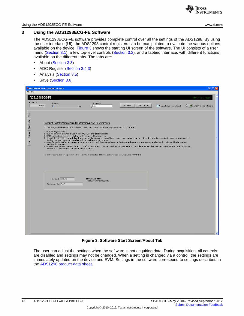
The ADS1298ECG-FE software provides complete control over all the settings of the ADS1298. By usingthe user interface (UI), the ADS1298 control registers can be manipulated to evaluate the various optionsavailable on the device. Figure 3 shows the starting UI screen of the software. The UI consists of a usermenu (Section 3.1), a few top-level controls (Section 3.2), and a tabbed interface, with different functionsavailable on the different tabs. The tabs are:
• About (Section 3.3)
• ADC Register (Section 3.4.3)
• Analysis (Section 3.5)
• Save (Section 3.6)
Figure 3. Software Start Screen/About Tab
The user can adjust the settings when the software is not acquiring data. During acquisition, all controlsare disabled and settings may not be changed. When a setting is changed via a control, the settings areimmediately updated on the device and EVM. Settings in the software correspond to settings described inthe ADS1298 product data sheet.
12 ADS1298ECG-FE/ADS1198ECG-FE SBAU171C–May 2010–Revised September 2012Submit Documentation Feedback
Copyright © 2010–2012, Texas Instruments Incorporated
www.ti.com Using the ADS1298ECG-FE Software
3.1 Application User Menu
The application user menu is located along the top of the application menu. It consists of two items: Fileand Help.
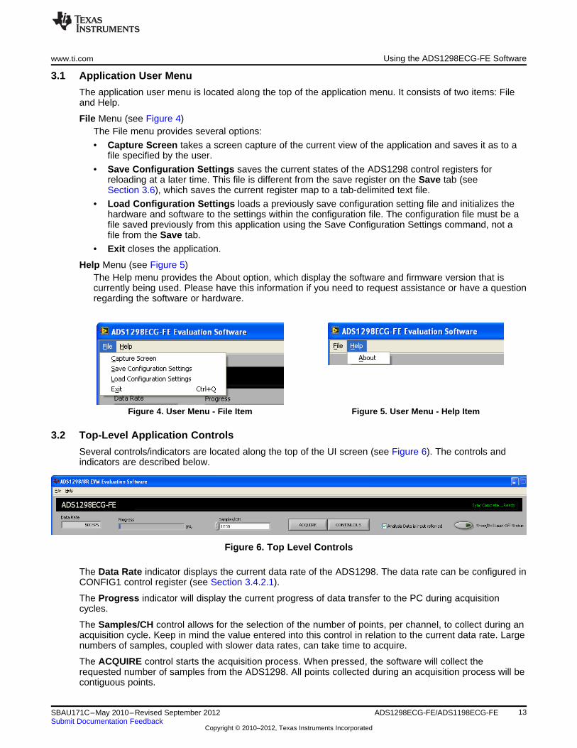
File Menu (see Figure 4)The File menu provides several options:
• Capture Screen takes a screen capture of the current view of the application and saves it as to afile specified by the user.
• Save Configuration Settings saves the current states of the ADS1298 control registers forreloading at a later time. This file is different from the save register on the Save tab (seeSection 3.6), which saves the current register map to a tab-delimited text file.
• Load Configuration Settings loads a previously save configuration setting file and initializes thehardware and software to the settings within the configuration file. The configuration file must be afile saved previously from this application using the Save Configuration Settings command, not afile from the Save tab.
• Exit closes the application.
Help Menu (see Figure 5)The Help menu provides the About option, which display the software and firmware version that iscurrently being used. Please have this information if you need to request assistance or have a questionregarding the software or hardware.
Figure 4. User Menu - File Item Figure 5. User Menu - Help Item
3.2 Top-Level Application Controls
Several controls/indicators are located along the top of the UI screen (see Figure 6). The controls andindicators are described below.
Figure 6. Top Level Controls
The Data Rate indicator displays the current data rate of the ADS1298. The data rate can be configured inCONFIG1 control register (see Section 3.4.2.1).
The Progress indicator will display the current progress of data transfer to the PC during acquisitioncycles.
The Samples/CH control allows for the selection of the number of points, per channel, to collect during anacquisition cycle. Keep in mind the value entered into this control in relation to the current data rate. Largenumbers of samples, coupled with slower data rates, can take time to acquire.
The ACQUIRE control starts the acquisition process. When pressed, the software will collect therequested number of samples from the ADS1298. All points collected during an acquisition process will becontiguous points.
13SBAU171C–May 2010–Revised September 2012 ADS1298ECG-FE/ADS1198ECG-FESubmit Documentation Feedback
Copyright © 2010–2012, Texas Instruments Incorporated
Using the ADS1298ECG-FE Software www.ti.com
The CONTINUOUS control starts a repeated acquisition process. This function acquires the requestedsamples and repeats the data acquisition until the button is turned off. Within a single acquisition cycle,the points will be contiguous, but from acquisition to acquisition, there may be points missing.
The Analysis Data input referred checkbox changes the displayed data that is read from the ADC.Checking the box displays the data input referred, while not checking displays the data as converted.
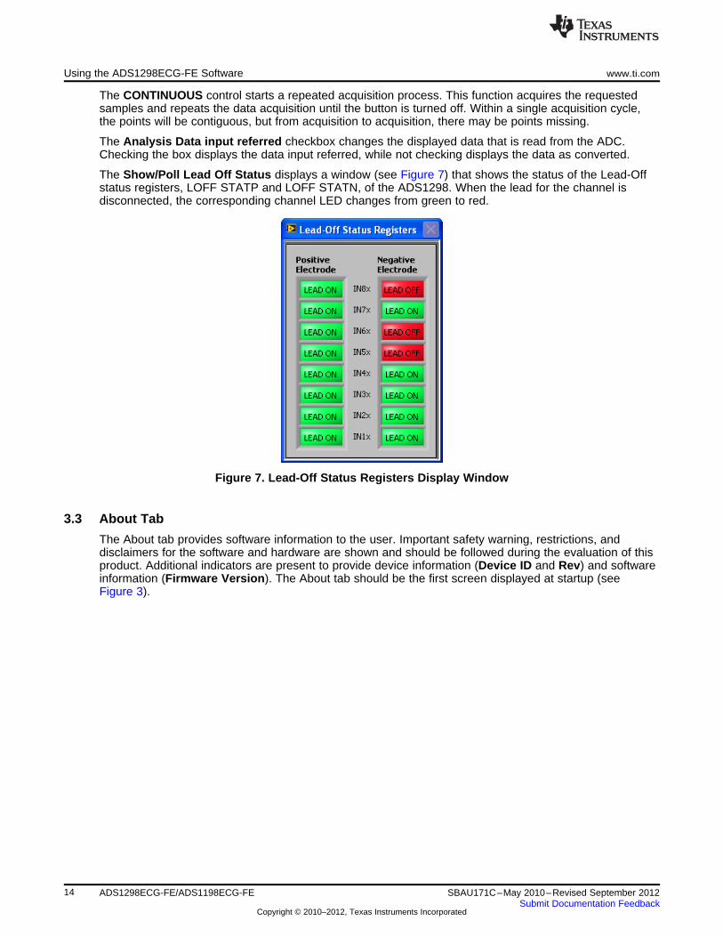
The Show/Poll Lead Off Status displays a window (see Figure 7) that shows the status of the Lead-Offstatus registers, LOFF STATP and LOFF STATN, of the ADS1298. When the lead for the channel isdisconnected, the corresponding channel LED changes from green to red.
Figure 7. Lead-Off Status Registers Display Window
3.3 About Tab
The About tab provides software information to the user. Important safety warning, restrictions, anddisclaimers for the software and hardware are shown and should be followed during the evaluation of thisproduct. Additional indicators are present to provide device information (Device ID and Rev) and softwareinformation (Firmware Version). The About tab should be the first screen displayed at startup (seeFigure 3).
14 ADS1298ECG-FE/ADS1198ECG-FE SBAU171C–May 2010–Revised September 2012Submit Documentation Feedback
Copyright © 2010–2012, Texas Instruments Incorporated
www.ti.com Using the ADS1298ECG-FE Software
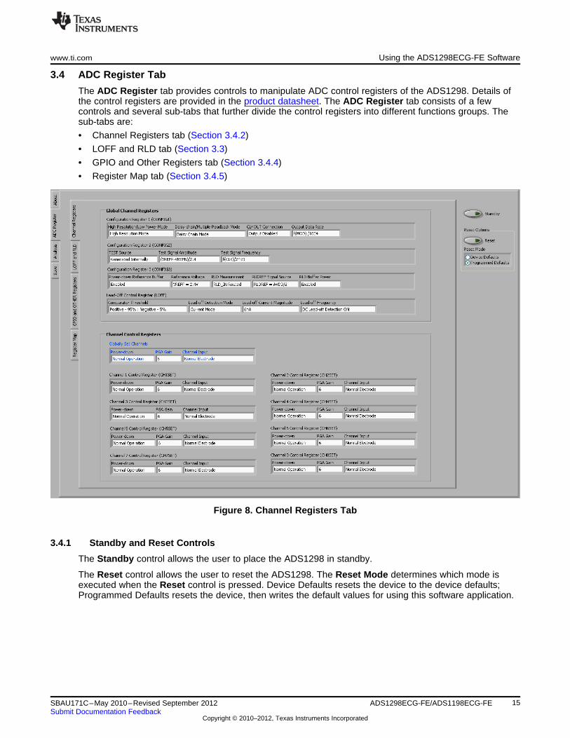
3.4 ADC Register Tab
The ADC Register tab provides controls to manipulate ADC control registers of the ADS1298. Details ofthe control registers are provided in the product datasheet. The ADC Register tab consists of a fewcontrols and several sub-tabs that further divide the control registers into different functions groups. Thesub-tabs are:
• Channel Registers tab (Section 3.4.2)
• LOFF and RLD tab (Section 3.3)
• GPIO and Other Registers tab (Section 3.4.4)
• Register Map tab (Section 3.4.5)
Figure 8. Channel Registers Tab
3.4.1 Standby and Reset Controls
The Standby control allows the user to place the ADS1298 in standby.
The Reset control allows the user to reset the ADS1298. The Reset Mode determines which mode isexecuted when the Reset control is pressed. Device Defaults resets the device to the device defaults;Programmed Defaults resets the device, then writes the default values for using this software application.
15SBAU171C–May 2010–Revised September 2012 ADS1298ECG-FE/ADS1198ECG-FESubmit Documentation Feedback
Copyright © 2010–2012, Texas Instruments Incorporated
22 Fm
To ADC Reference Inputs
VCAP1
10 Fm
VREFP
VREFN
Bandgap2.4V or 4V
AVSS
R1(1)
R3(1)
R2(1)
Using the ADS1298ECG-FE Software www.ti.com
3.4.2 Channel Registers Tab (ADC Register)
The Channel Register tab provides access to control registers that control different properties/settings forthe ADC channels. The control register are grouped into two groups: Global Channel Registers andChannel Control Registers.
3.4.2.1 Global Channel Registers
The Global Channel Registers box includes Configuration Register 1 (CONFIG1), Configuration Register 2(CONFIG2), Configuration Register 3 (CONFIG3), and Lead Off Control Register (LOFF). The upper halfof Figure 8 shows the section of the UI panel that allows manipulation and control of these registers.
Configuration Register 1 enables the user to control the resolution mode, enable the daisy-chainconfiguration options, and program the data rate.
NOTE: Since the HR bit is not available in the ADS1198, the Configuration Register 1 control will notshow this control when testing the ADS1198.
Configuration Register 2 enables the user to select an internal square wave test source amplitude of±1mV or ±2mV and a frequency of DC, 2Hz (fCLK/221), or 4Hz (fCLK/220).
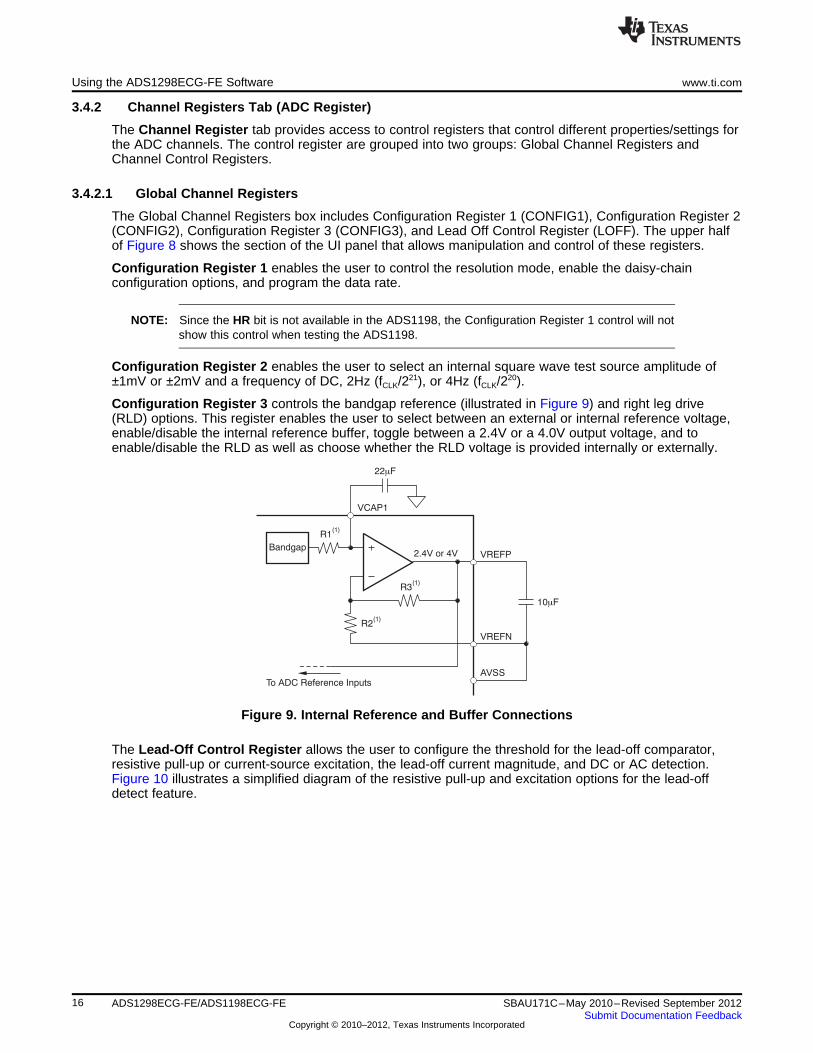
Configuration Register 3 controls the bandgap reference (illustrated in Figure 9) and right leg drive(RLD) options. This register enables the user to select between an external or internal reference voltage,enable/disable the internal reference buffer, toggle between a 2.4V or a 4.0V output voltage, and toenable/disable the RLD as well as choose whether the RLD voltage is provided internally or externally.
Figure 9. Internal Reference and Buffer Connections
The Lead-Off Control Register allows the user to configure the threshold for the lead-off comparator,resistive pull-up or current-source excitation, the lead-off current magnitude, and DC or AC detection.Figure 10 illustrates a simplified diagram of the resistive pull-up and excitation options for the lead-offdetect feature.
16 ADS1298ECG-FE/ADS1198ECG-FE SBAU171C–May 2010–Revised September 2012Submit Documentation Feedback
Copyright © 2010–2012, Texas Instruments Incorporated
MUX[2:0] = 101
TempPMUX[2:0] = 100
MvddP(1) MUX[2:0] = 011
From LoffP
MUX[2:0] = 000
MUX[2:0] = 110
MUX[2:0] = 001
To PgaP
To PgaNMUX[2:0] = 001
RLDIN
MUX[2:0] = 010RLD_MEAS
AND
MUX[2:0] = 111
VINP
VINNMUX[2:0] = 000
From LoffN
RLD_REF
MUX[2:0] = 010RLD_MEAS
AND
MvddN(1)
TempNMUX[2:0] = 100
MUX[2:0] = 101
ADS129x
MUX
TestP
TestN
TESTP_PACE_OUT1
INT_TEST
INT_TEST
TESTN_PACE_OUT2
INT_TEST
INT_TEST
MUX[2:0] = 011
EMIFilter
(AVDD + AVSS)
2
a) Pull-Up/Pull-Down Resistors b) Current Source
PGA
10MW
10MW
AVDD
INP
INN
PGA
AVDD
INP
INN
ADS129xADS129x
www.ti.com Using the ADS1298ECG-FE Software
Figure 10. Lead-Off Excitation Options
3.4.2.2 Channel Control Registers
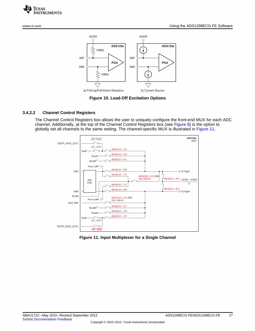
The Channel Control Registers box allows the user to uniquely configure the front-end MUX for each ADCchannel. Additionally, at the top of the Channel Control Registers box (see Figure 8) is the option toglobally set all channels to the same setting. The channel-specific MUX is illustrated in Figure 11.
Figure 11. Input Multiplexer for a Single Channel
17SBAU171C–May 2010–Revised September 2012 ADS1298ECG-FE/ADS1198ECG-FESubmit Documentation Feedback
Copyright © 2010–2012, Texas Instruments Incorporated

Using the ADS1298ECG-FE Software www.ti.com
3.4.3 LOFF and RLD Tab (ADC Register)
The LOFF and RLD tab provides control over the Lead-Off Detection and Current Control Registers andthe Right Leg Derivation Control Registers. The tab and controls are shown in Figure 12.
Figure 12. LOFF and RLD Tab
3.4.3.1 Lead-Off Detection and Current Direction Control Registers
The first two arrays of controls (Lead Off Sense) enable lead-off detection for both the positive andnegative channels, LOFF_SENSP and LOFF_SENSN. By pressing the buttons, lead-off detection isenabled for each channel individually and for each input (positive and negative). Set All LOFFP Bits andSet All LOFFN Bits allow the user to turn on or off all the enable bits at once instead of clicking eachindividual channel control.
The third array of controls (Lead Off Current Direction) determines the current direction used for lead-offdetection when an excitation signal is selected as a pull-up/pull-down resistor. Each channel is controlledindividually by selecting the button that corresponds to the desired channel to manipulate. When thebutton is not illuminated, LOFF_FLIP = 0 (INP is pulled-up to AVDD and INN is pulled-down to ground).When the button is pressed/illuminated, LOFF_FLIP = 1 (INP is pulled-down to ground and INN is pulled-up to AVDD). Further details of these registers and lead-off function are located in the ApplicationsSection of the device data sheet.
18 ADS1298ECG-FE/ADS1198ECG-FE SBAU171C–May 2010–Revised September 2012Submit Documentation Feedback
Copyright © 2010–2012, Texas Instruments Incorporated
4-Bit
DAC
To ADC
LOFF_STATP
LOFF_STATN
COMP_TH[2:0]
VINP
VINN
PGA
www.ti.com Using the ADS1298ECG-FE Software
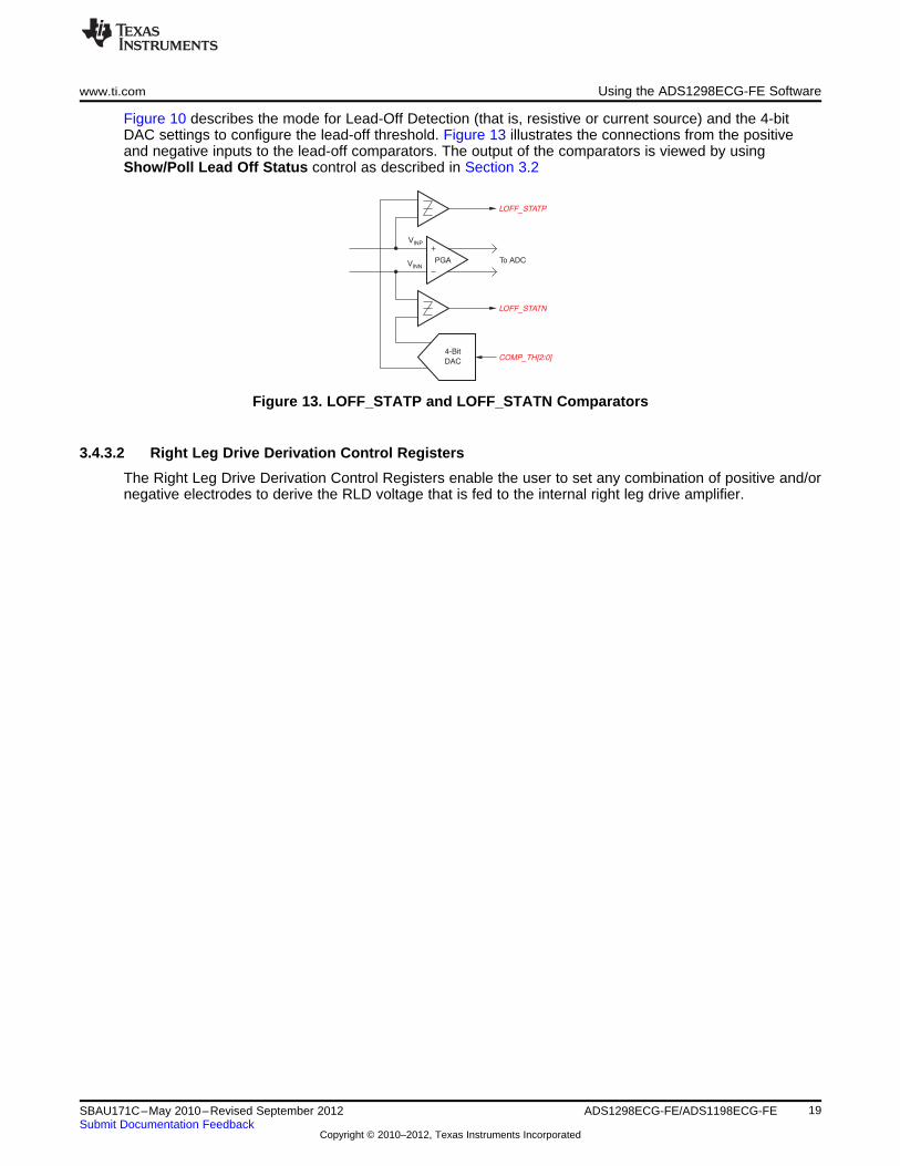
Figure 10 describes the mode for Lead-Off Detection (that is, resistive or current source) and the 4-bitDAC settings to configure the lead-off threshold. Figure 13 illustrates the connections from the positiveand negative inputs to the lead-off comparators. The output of the comparators is viewed by usingShow/Poll Lead Off Status control as described in Section 3.2
Figure 13. LOFF_STATP and LOFF_STATN Comparators
3.4.3.2 Right Leg Drive Derivation Control Registers
The Right Leg Drive Derivation Control Registers enable the user to set any combination of positive and/ornegative electrodes to derive the RLD voltage that is fed to the internal right leg drive amplifier.
19SBAU171C–May 2010–Revised September 2012 ADS1298ECG-FE/ADS1198ECG-FESubmit Documentation Feedback
Copyright © 2010–2012, Texas Instruments Incorporated

Using the ADS1298ECG-FE Software www.ti.com
3.4.4 GPIO and OTHER Registers Tab (ADC Register)
The GPIO and Other Registers tab, located under the Analysis tab, includes controls for GPIO1 throughGPIO4, respiration phase and frequency, routing of the Wilson amplifiers, and derivation of the Goldbergerterminals. Figure 14 shows the GPIO and OTHER Registers tab and all controls contained on the tab.
Figure 14. GPIO and OTHER Register Tab
The General-Purpose I/O Register (GPIO) controls the four general-purpose I/O pins. Each GPIO can beset as an input or an output via GPIOCx controls. If the output is selected, the GPIODx control is enabledallowing the user to set the value to output. If the GPIO is selected as an input, the GPIODx control isdisabled and shows the value of the GPIO. If any of the GPIOs are selected as inputs, the Read GPIOcontrol is enabled which allows the GPIODx values to be updated to the current GPIO value.
The PACE Detect Register does not enable a special PACE measurement mode. The register allows forenabling and configuration of the PACE amplifiers. PACE Amplifier 1 can connect to input channels 1-4and Pace Amplifier 2 can connect to input channels 5-8.
The Configuration 4 Register allows control over the Respiration Frequency, WCT connection to theRLD and lead-off comparator enable status.
NOTE: The Respiration Frequency control is disable since the functionality is not available on theADS1298 and ADS1198.
The Respiration Control Register is disabled for the ADS1298 and not available for the ADS1198.
20 ADS1298ECG-FE/ADS1198ECG-FE SBAU171C–May 2010–Revised September 2012Submit Documentation Feedback
Copyright © 2010–2012, Texas Instruments Incorporated

Wcta
8:1 MUX
WC
T1[2
:0]
IN4N
IN4P
IN3N
IN3P
IN2N
IN2P
WCT
IN1N
IN1P
Wctb
8:1 MUX
WC
T2[5
:3]
Wctc
8:1 MUX
WC
T2[2
:0]
To ChannelPGAs
ADS1294/6/8
30kW 30kW 30kW
80pF
AVSS
Wcta
8:1 MUXW
CT
1[2
:0]
IN4N
IN4P
IN3N
IN3P
IN2N
IN2P
IN7N
IN7P
IN6N
IN6P
IN5N
IN5P
IN1N
IN1P
Wctb
8:1 MUX
WC
T2[5
:3]
Wctc
8:1 MUX
WC
T2[2
:0]
To ChannelPGAs
ADS1298
avF_ch6 avF_ch5 avF_ch7
avF_ch4
To ChannelPGAs
(a) Wilson Central Lead Routing (b) Wilson Augmented Lead Routing
www.ti.com Using the ADS1298ECG-FE Software
3.4.4.1 Wilson Central and Augmented Lead Registers
The Wilson Central Voltage (an average voltage between the right arm [RA], left arm [LA], and left leg [LL]connections) can be derived from any combination of positive and negative terminals from channels 1-4and routed to the WCT pin. Likewise, the Augmented Leads (AVF, AVL, AVR) may be derived fromchannels 1-4 and routed to the negative terminal of channels 5, 6, and 7. Figure 15 shows theseconfigurations; Figure 15a illustrates the central lead routing, and Figure 15b shows the augmented leadrouting.
Figure 15. Wilson Central and Augmented Lead Routing Diagrams
21SBAU171C–May 2010–Revised September 2012 ADS1298ECG-FE/ADS1198ECG-FESubmit Documentation Feedback
Copyright © 2010–2012, Texas Instruments Incorporated
Using the ADS1298ECG-FE Software www.ti.com
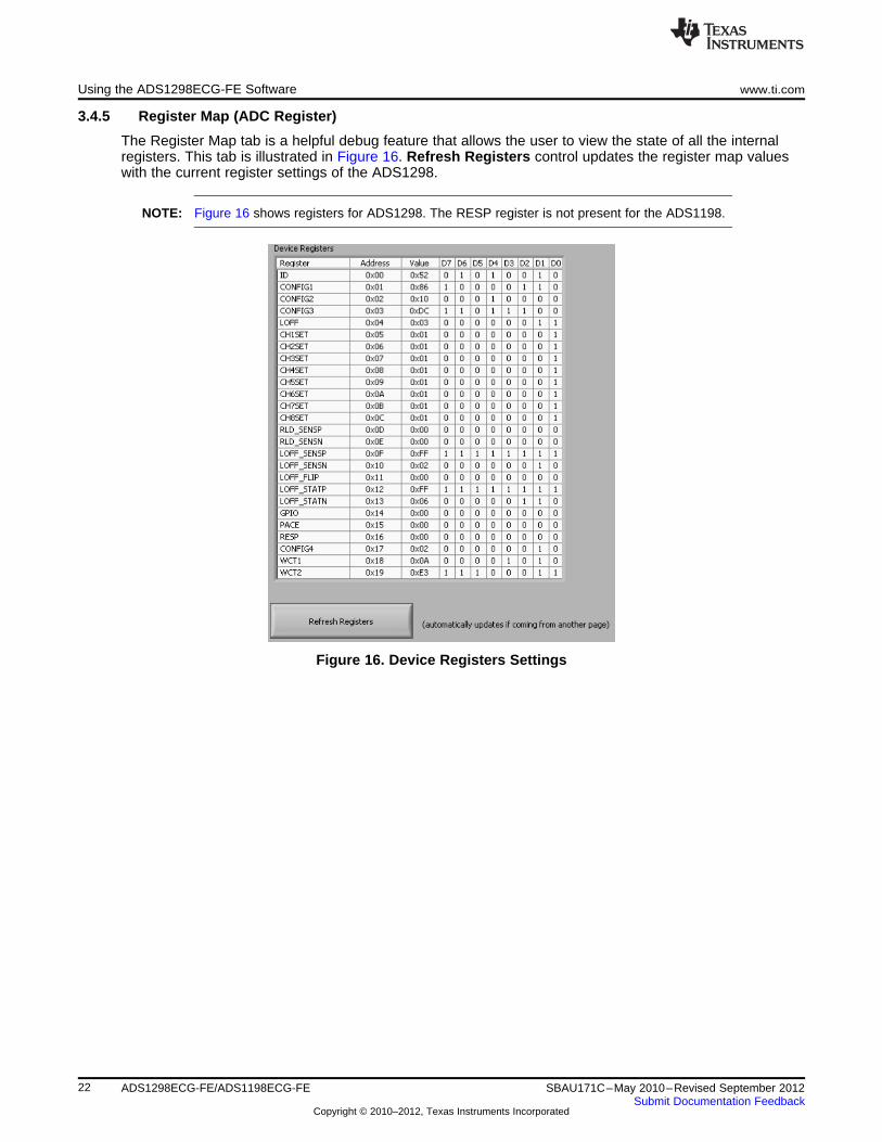
3.4.5 Register Map (ADC Register)
The Register Map tab is a helpful debug feature that allows the user to view the state of all the internalregisters. This tab is illustrated in Figure 16. Refresh Registers control updates the register map valueswith the current register settings of the ADS1298.
NOTE: Figure 16 shows registers for ADS1298. The RESP register is not present for the ADS1198.
Figure 16. Device Registers Settings
22 ADS1298ECG-FE/ADS1198ECG-FE SBAU171C–May 2010–Revised September 2012Submit Documentation Feedback
Copyright © 2010–2012, Texas Instruments Incorporated
www.ti.com Using the ADS1298ECG-FE Software
3.5 Analysis Tab
The Analysis tab provides access to the different analysis options that are available using the software.The different analyses are grouped by sub-tabs:
• Scope tab (Section 3.5.1)
• Histogram tab (Section 3.5.2)
• FFT tab (Section 3.5.3)
• ECG tab (Section 3.5.4)
3.5.1 Scope Tab (Anaysis)
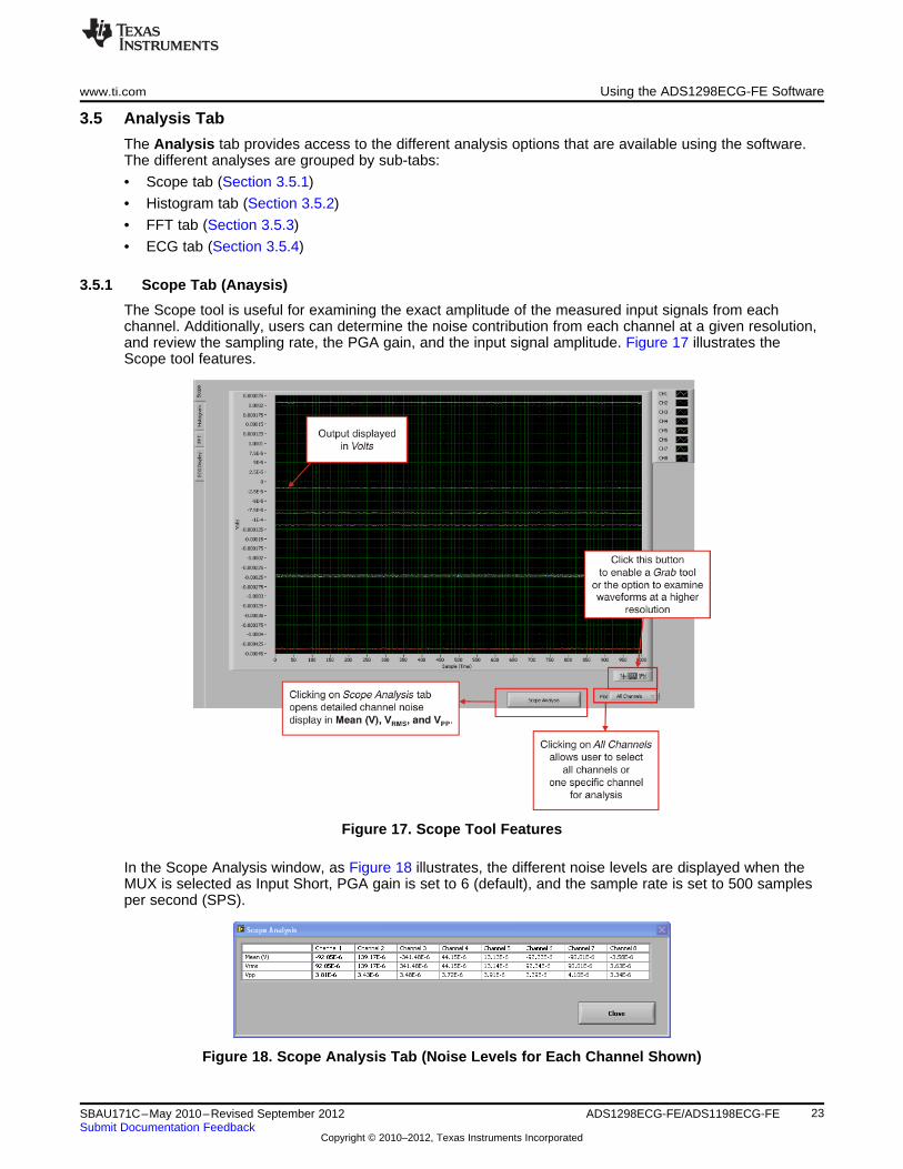
The Scope tool is useful for examining the exact amplitude of the measured input signals from eachchannel. Additionally, users can determine the noise contribution from each channel at a given resolution,and review the sampling rate, the PGA gain, and the input signal amplitude. Figure 17 illustrates theScope tool features.
Figure 17. Scope Tool Features
In the Scope Analysis window, as Figure 18 illustrates, the different noise levels are displayed when theMUX is selected as Input Short, PGA gain is set to 6 (default), and the sample rate is set to 500 samplesper second (SPS).
Figure 18. Scope Analysis Tab (Noise Levels for Each Channel Shown)
23SBAU171C–May 2010–Revised September 2012 ADS1298ECG-FE/ADS1198ECG-FESubmit Documentation Feedback
Copyright © 2010–2012, Texas Instruments Incorporated
Using the ADS1298ECG-FE Software www.ti.com
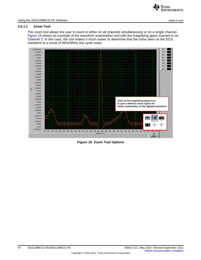
3.5.1.1 Zoom Tool
The zoom tool allows the user to zoom in either on all channels simultaneously or on a single channel.Figure 19 shows an example of the waveform examination tool with the magnifying glass zoomed in onChannel 2. In this case, the tool makes it much easier to determine that the noise seen on the ECGwaveform is a result of 50Hz/60Hz line cycle noise.
Figure 19. Zoom Tool Options
24 ADS1298ECG-FE/ADS1198ECG-FE SBAU171C–May 2010–Revised September 2012Submit Documentation Feedback
Copyright © 2010–2012, Texas Instruments Incorporated
www.ti.com Using the ADS1298ECG-FE Software
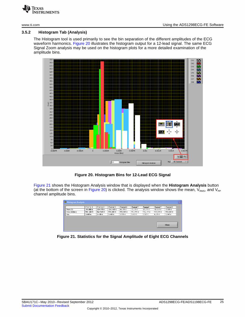
3.5.2 Histogram Tab (Analysis)
The Histogram tool is used primarily to see the bin separation of the different amplitudes of the ECGwaveform harmonics. Figure 20 illustrates the histogram output for a 12-lead signal. The same ECGSignal Zoom analysis may be used on the histogram plots for a more detailed examination of theamplitude bins.
Figure 20. Histogram Bins for 12-Lead ECG Signal
Figure 21 shows the Histogram Analysis window that is displayed when the Histogram Analysis button(at the bottom of the screen in Figure 20) is clicked. The analysis window shows the mean, VRMS, and VPP
channel amplitude bins.
Figure 21. Statistics for the Signal Amplitude of Eight ECG Channels
25SBAU171C–May 2010–Revised September 2012 ADS1298ECG-FE/ADS1198ECG-FESubmit Documentation Feedback
Copyright © 2010–2012, Texas Instruments Incorporated

Using the ADS1298ECG-FE Software www.ti.com
3.5.3 FFT Tab
The FFT tool allows the user to examine the channel-specific spectrum as well as typical figures of meritsuch as SNR, THD, ENOB, and CMRR. Each feature is numbered below and described in detail in thefollowing subsections. Figure 22 illustrates an FFT plot for a normal electrode configuration.
Figure 22. FFT Graph of Normal Electrode Configuration
1 - Coherent Frequency CalculatorCoherent sampling in an FFT is defined as FAIN/FSAMPLE = NWINDOW/NTOTAL, where:
• FAIN is the input frequency
• FSAMPLE is the sampling frequency of the ADS1298
• NWINDOW is the number of odd integer cycles during a given sampling period
• NTOTAL is the number of data points (in powers of 2) that is used to create the FFTIf the conditions for coherent sampling can be met, the FFT results for a periodic signal will beoptimized. The Ideal AIN Frequency is a value that is calculated based on the sampling rate, such thatthe coherent sampling criteria can be met.
2 - AC Analysis ParametersThis section of the tool allows the user to dictate the number of harmonics, DC leakage bins, harmonicleakage bins, and fundamental leakage bins that are used in the creation of various histograms.Pressing the Windowing button, illustrated in Figure 23, allows the user to evaluate the FFT graphunder a variety of different windows. Note that pressing the Reference button toggles between dBFS(decibels, full-scale) and dBc (decibels to carrier).
Figure 23. AC Analysis Parameters: Windowing Options
26 ADS1298ECG-FE/ADS1198ECG-FE SBAU171C–May 2010–Revised September 2012Submit Documentation Feedback
Copyright © 2010–2012, Texas Instruments Incorporated
www.ti.com Using the ADS1298ECG-FE Software
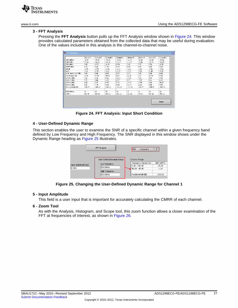
3 - FFT AnalysisPressing the FFT Analysis button pulls up the FFT Analysis window shown in Figure 24. This windowprovides calculated parameters obtained from the collected data that may be useful during evaluation.One of the values included in this analysis is the channel-to-channel noise.
Figure 24. FFT Analysis: Input Short Condition
4 - User-Defined Dynamic Range
This section enables the user to examine the SNR of a specific channel within a given frequency banddefined by Low Frequency and High Frequency. The SNR displayed in this window shows under theDynamic Range heading as Figure 25 illustrates.
Figure 25. Changing the User-Defined Dynamic Range for Channel 1
5 - Input AmplitudeThis field is a user input that is important for accurately calculating the CMRR of each channel.
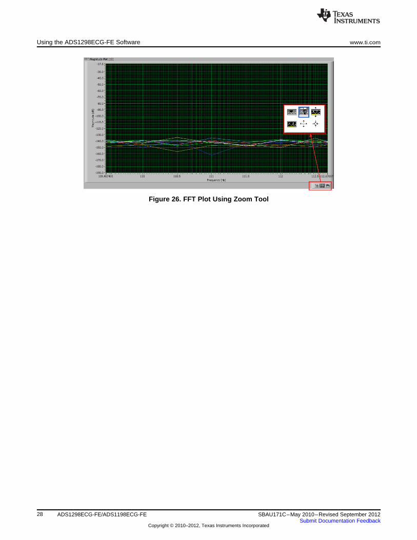
6 - Zoom ToolAs with the Analysis, Histogram, and Scope tool, this zoom function allows a closer examination of theFFT at frequencies of interest, as shown in Figure 26.
27SBAU171C–May 2010–Revised September 2012 ADS1298ECG-FE/ADS1198ECG-FESubmit Documentation Feedback
Copyright © 2010–2012, Texas Instruments Incorporated
Using the ADS1298ECG-FE Software www.ti.com
Figure 26. FFT Plot Using Zoom Tool
28 ADS1298ECG-FE/ADS1198ECG-FE SBAU171C–May 2010–Revised September 2012Submit Documentation Feedback
Copyright © 2010–2012, Texas Instruments Incorporated
www.ti.com Using the ADS1298ECG-FE Software
3.5.4 ECG Tab (Analysis)
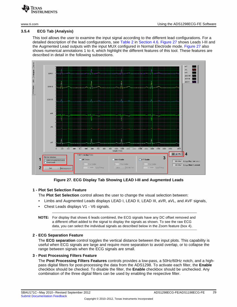
This tool allows the user to examine the input signal according to the different lead configurations. For adetailed description of the lead configurations, see Table 2 in Section 4.6. Figure 27 shows Leads I-III andthe Augmented Lead outputs with the input MUX configured in Normal Electrode mode. Figure 27 alsoshows numerical annotations 1 to 4, which highlight the different features of this tool. These features aredescribed in detail in the following subsections.
Figure 27. ECG Display Tab Showing LEAD I-III and Augmented Leads
1 - Plot Set Selection FeatureThe Plot Set Selection control allows the user to change the visual selection between:
• Limbs and Augmented Leads displays LEAD I, LEAD II, LEAD III, aVR, aVL, and AVF signals,
• Chest Leads displays V1 - V6 signals.
NOTE: For display that shows 6 leads combined, the ECG signals have any DC offset removed anda different offset added to the signal to display the signals as shown. To see the raw ECGdata, you can select the individual signals as described below in the Zoom feature (box 4).
2 - ECG Separation FeatureThe ECG separation control toggles the vertical distance between the input plots. This capability isuseful when ECG signals are large and require more separation to avoid overlap, or to collapse therange between signals when the ECG signals are small.
3 - Post Processing Filters FeatureThe Post Processing Filters Features controls provides a low-pass, a 50Hz/60Hz notch, and a high-pass digital filters for post-processing the data from the ADS1298. To activate each filter, the Enablecheckbox should be checked. To disable the filter, the Enable checkbox should be unchecked. Anycombination of the three digital filters can be used by enabling the respective filter.
29SBAU171C–May 2010–Revised September 2012 ADS1298ECG-FE/ADS1198ECG-FESubmit Documentation Feedback
Copyright © 2010–2012, Texas Instruments Incorporated
Using the ADS1298ECG-FE Software www.ti.com
The low-pass filter controls a digital low-pass filter, whose order and cutoff frequency are controlledusing the Filter Order and Cutoff Freq controls in the low-pass filter part of the Post ProcessingFilters group (left side of the box).The notch filter provides a 50Hz/60Hz notch filter, whose order and 50Hz/60Hz notch selection arecontrolled using the Filter Order and Notch Freq controls in the low-pass filter part of the PostProcessing Filters group (center of the box).The high-pass filter controls a digital high-pass filter, whose order and cutoff frequency arecontrolled using the Filter Order and Cutoff Freq controls in the high-pass filter part of the PostProcessing Filters group (right side of the box).
NOTE: The digital filters are not part of the ADS1298. These are digital filters implemented in the UIto aid in the evaluation of the ADS1298ECG-FE.
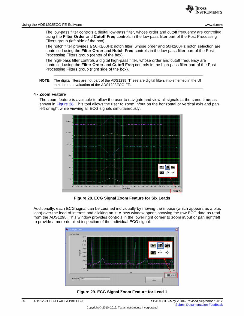
4 - Zoom FeatureThe zoom feature is available to allow the user to navigate and view all signals at the same time, asshown in Figure 28. This tool allows the user to zoom in/out on the horizontal or vertical axis and panleft or right while viewing all ECG signals simultaneously.
Figure 28. ECG Signal Zoom Feature for Six Leads
Additionally, each ECG signal can be zoomed individually by moving the mouse (which appears as a plusicon) over the lead of interest and clicking on it. A new window opens showing the raw ECG data as readfrom the ADS1298. This window provides controls in the lower right corner to zoom in/out or pan right/leftto provide a more detailed inspection of the individual ECG signal.
Figure 29. ECG Signal Zoom Feature for Lead 1
30 ADS1298ECG-FE/ADS1198ECG-FE SBAU171C–May 2010–Revised September 2012Submit Documentation Feedback
Copyright © 2010–2012, Texas Instruments Incorporated

www.ti.com Using the ADS1298ECG-FE Software
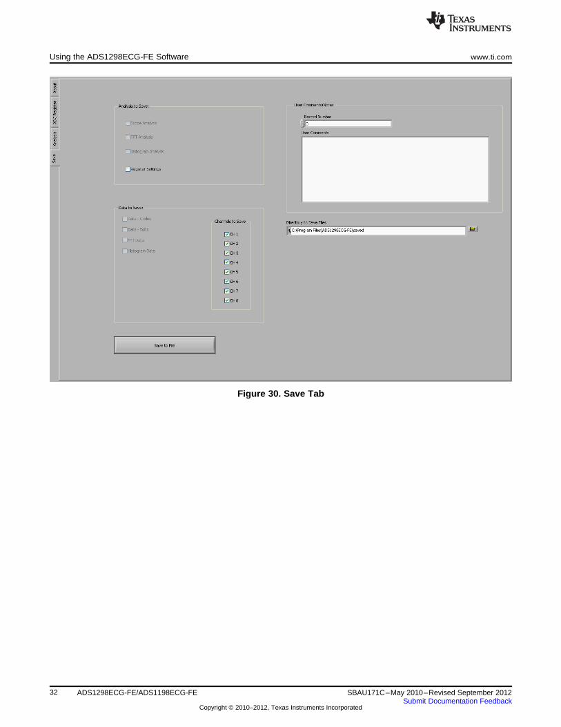
3.6 Save Tab
The Save tab provides the user the ability to save the collected data for a record of the evaluation orfurther analysis. Reference the previous sections for the list of the anlaysis data available for eachanalysis.
The Analysis to Save group allows the user to save the different analysis calculations that were performedon the data.
• Scope Analysis saves the scope analysis data available from the scope analysis pop-up window
• FFT Analysis saves the FFT analysis data available from the FFT analysis pop-up window.
• Histogram Analysis saves the histogram analysis data available from the histogram analysis pop-upwindow.
• Register Settings saves the current settings from the register map and can be useful to obtain theregister values for your specific device configuration. Saving the register map in this format is not beconfused with saving your register settings for reloading into the software at another time (seeSection 3.1).
Each item will be saved if the corresponding checkbox is checked.
The Data to Save group allows the user to save the various data sets collected from the ADS1298. TheCH x controls allow the user to specify which channels will be saved for each of the data selections made.
• Data - Codes selects the raw data (in codes format) to be saved to a file.
• Data - Volts selects the raw data (converted to voltage) to be saved to a file.
• FFT Data selects the calculated FFT data to be saved to a file. Note: This is not raw data; it is thefrequency bin and magnitude data that was calculated by the UI.
• Histogram Data selected the calculated Histogram data to be saved to a file. Note: This is not rawdata; it is the code bin and number of occurrences data that was calculated by the UI.
The User Comments/Notes group allows the user to indicate a Record Number and User Commentsthat are saved with each file. This data permits the user to distinguish different data sets from oneanother.
The Directory to Save Files is the directory where all the saved files will be placed. The user can select adirectory by pressing the folder button (located to the right of the control). Each data file that is saved isautomatically named to prevent overwriting of files.
The Save To File button saves all the data files that were selected using the checkboxes to the selecteddirectory.
31SBAU171C–May 2010–Revised September 2012 ADS1298ECG-FE/ADS1198ECG-FESubmit Documentation Feedback
Copyright © 2010–2012, Texas Instruments Incorporated
Using the ADS1298ECG-FE Software www.ti.com
Figure 30. Save Tab
32 ADS1298ECG-FE/ADS1198ECG-FE SBAU171C–May 2010–Revised September 2012Submit Documentation Feedback
Copyright © 2010–2012, Texas Instruments Incorporated

www.ti.com ADS1x98ECG-FE Input Signals
4 ADS1x98ECG-FE Input Signals
NOTE: Before evaluating specific ECG functions, it is recommended that the user acquire data withinputs shorted internally. This configuration ensures that the board is operating properly.
4.1 Input Short Testing
By default, the EVM powers up with the individual channels to an internal short with a data rate of 500SPSand a PGA gain of 6. Once the Acquire button is pressed, the Scope Analysis should reflect input-referred VPP values less than 5µVPP
4.2 Internal Test Signals Input
Configuration Register 2 controls the signal amplitude and frequency of an internally-generated squarewave test signal. The primary purpose of this test signal is to verify the functionality of the front-end MUX,the PGA, and the ADC. The test signals may be viewed on the ECG Display tab, as Figure 31 shows.Detailed instructions for using the ECG Display tab are provided in Section 3.5.4.
Figure 31. Example of Internal Test Signals Viewed on the ECG Display Tab
33SBAU171C–May 2010–Revised September 2012 ADS1298ECG-FE/ADS1198ECG-FESubmit Documentation Feedback
Copyright © 2010–2012, Texas Instruments Incorporated

Temperature ( C) =°Temperature Reading ( V) 145,300 Vm - m
490 V/ Cm °
+ 25 C°
2x
1x
1x
8x
AVDD
AVSS
ADS1x98ECG-FE Input Signals www.ti.com
4.3 Temperature Sensor
The internal temperature sensor on the ADS1298 is shown in Figure 32. When the internal MUX is routedto the temperature sensor input, the ADC internal temperature is calculated from the ADC output voltageusing Equation 1.
Figure 32. Internal Temperature Sensor
(1)
The ADC can be configured to give a temperature reading by selecting the Temperature Sensor option onthe Channel Control Registers GUI (see Section 3.4.2.2) and verified using the Scope tab as shown inFigure 33. The number 0.1447V (on the y-axis) can be calculated as a temperature using Equation 1:
Temperature = (0.1447 – 0.145300) / 0.00049 + 25 = 23.78°CA more detailed description of the Scope tab is provided in Section 3.5.1.
Figure 33. Eight-Channel Read of Internal Temperature
34 ADS1298ECG-FE/ADS1198ECG-FE SBAU171C–May 2010–Revised September 2012Submit Documentation Feedback
Copyright © 2010–2012, Texas Instruments Incorporated
www.ti.com ADS1x98ECG-FE Input Signals
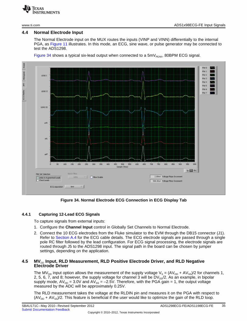
4.4 Normal Electrode Input
The Normal Electrode input on the MUX routes the inputs (VINP and VINN) differentially to the internalPGA, as Figure 11 illustrates. In this mode, an ECG, sine wave, or pulse generator may be connected totest the ADS1298.
Figure 34 shows a typical six-lead output when connected to a 5mVPEAK, 80BPM ECG signal.
Figure 34. Normal Electrode ECG Connection in ECG Display Tab
4.4.1 Capturing 12-Lead ECG Signals
To capture signals from external inputs:
1. Configure the Channel Input control in Globally Set Channels to Normal Electrode.
2. Connect the 10 ECG electrodes from the Fluke simulator to the EVM through the DB15 connector (J1).Refer to Section A.4 for the ECG cable details. The ECG electrode signals are passed through a singlepole RC filter followed by the lead configuration. For ECG signal processing, the electrode signals arerouted through J5 to the ADS1298 input. The signal path in the board can be chosen by jumpersettings, depending on the application.
4.5 MVDD Input, RLD Measurement, RLD Positive Electrode Driver, and RLD NegativeElectrode Driver
The MVDD input option allows the measurement of the supply voltage VS = (AVDD + AVSS)/2 for channels 1,2, 5, 6, 7, and 8; however, the supply voltage for channel 3 will be DVDD/2. As an example, in bipolarsupply mode, AVDD = 3.0V and AVSS = –2.5V. Therefore, with the PGA gain = 1, the output voltagemeasured by the ADC will be approximately 0.25V.
The RLD measurement takes the voltage at the RLDIN pin and measures it on the PGA with respect to(AVDD + AVSS)/2. This feature is beneficial if the user would like to optimize the gain of the RLD loop.
35SBAU171C–May 2010–Revised September 2012 ADS1298ECG-FE/ADS1198ECG-FESubmit Documentation Feedback
Copyright © 2010–2012, Texas Instruments Incorporated
ADS1x98ECG-FE Input Signals www.ti.com
The voltage used to derive the right leg drive for both the positive and negative electrodes may also bemeasured with respect to (AVDD + AVSS)/2.
4.6 Lead Derivation
The EVM is configured to generate the 12 ECG signals using 10 electrodes connected to the eight ADCchannels. Lead I, Lead II, and V1-V6 are computed in the analog domain, while the augmented leads andLead III are computed digitally. The channel assignments are described in Table 2.
• LA = Left Arm
• LL = Left Leg
• RA = Right Arm
Table 2. ADS1298 Lead Measurements
ADS1298 Input Channels Lead (1)
1 V6 = V6 – WCT
2 LEAD I = LA – RA
3 LEAD II = LL – RA
4 V2 = V2 – WCT
5 V3 = V3 – WCT
6 V4 = V4 – WCT
7 V5 = V5 – WCT
8 V1 = V1 – WCT(1) WCT = (LA + RA + LL)/3
Table 3. Derived Lead Calculations
Derived Lead Formula Used to Calculate
LEAD III LL - RA - LA = LEAD II - LEAD I
aVR RA - (LA + LL) / 2 = - (LEAD I + LEAD II) / 2
aVL LA - (RA +LL) / 2 = LEAD I - LEAD II / 2
aVF LL - (RA + LA) / 2 = LEAD II - LEAD I /2
4.7 Wilson Center Terminal (WCT)
The Wilson Center Terminal voltage is internally generated by the ADS1298 device. The WCT1 andWCT2 registers provide controls to select any of the eight inputs (CH1P to CH4P, CH1M to CH4M) forrouting to the three integrated WCT amplifiers.
The ADS1298ECG-FE is configured for 12-lead ECG inputs, with the limb electrodes connected as shownin Table 2. During EVM power-up, the firmware configures the device to route CH2P, CH2M, and CH3P(RA, LA, LL) to the internal buffers. This configuration generates a signal at the WCT pin equal to (RA +LA + LL)/3. By installing JP16, the WCT is routed to the single-ended channels to achieve the desiredsignals.
4.8 Right Leg Drive
The RL electrode is driven directly by the RLD signal generated on-chip by the ADS1298. The bandwidthof the RLD loop is determined by R8 (392kΩ) and C20 (10nF). Users can change these values to set thebandwidth based on their specific application. The loop stability is determined by the user’s specificsystem. Therefore, adjustment of the feedback component values may be required to ensure stability ifadditional filtering components and long cables are added before the ADS1298ECG-FE.
In a typical application, the RLD signal is implemented as the average of RA, LA, and LL. For systemflexibility, the ADS1298 allows the user to select any combination of the electrodes to generate the RLD(see ADS1298 data sheet or ADS1198 data sheet for more details).
36 ADS1298ECG-FE/ADS1198ECG-FE SBAU171C–May 2010–Revised September 2012Submit Documentation Feedback
Copyright © 2010–2012, Texas Instruments Incorporated

www.ti.com ADS1x98ECG-FE Input Signals
4.8.1 RLD Common Mode Voltage
The RLD common mode voltage can be set to (AVDD+AVSS)/2 or to an externally provided source. If theapplication requires the common mode to be set to any voltage other than mid-supply, this can beaccomplished by setting the appropriate bit in the Configuration 3 Register. On the ADS1298ECG-FE, theexternal RLDREF voltage is set using resistor R1 and adjustable resistor R2 (R1 and R2 are not installedby default).
During power-up, the firmware configures the device for internal RLDREF operation. To configure the RLDcircuitry manually, use the following steps and the controls found on the ADC Register tab.
1. Verify that the Channel Input is set to the Normal Electrode mode for all channels (ChannelRegisters tab).
2. In CONFIG3 control register (Channel Registers tab):
• Enable the RLD Buffer (RLD Buffer Power = Enable)
• Set the internal RLD reference (RLDREF Signal Source)
3. Select the electrodes for the RLD loop from the Right Leg Drive Derivation Control Registers controls(LOFF and RLD tab)
Once these steps are completed, measure and verify that the voltage on either side of R38 is close tomid-supply. This measurement confirms whether the RLD loop is functional.
The on-chip RLD signal can be fed back into the ADS1298 by shorting JP1. This RLD signal can then besent to the ADC (to measure for debug purposes) or to other electrodes for driving (to change thereference drive in case the RL electrode falls off). Refer to the ADS1298 product data sheet or ADS1198data sheet for additional details.
4.8.2 Driving the RLD Cable Shield
Apart from the RLD signal, the ADS1298ECG-FE also offers three options to drive the cable shield:
• In-phase RLD signal
• Out-of-phase RLD signal
• Board AGNDTable 4 summarizes the configuration of JP15 and JP17 for each of the options.
Table 4. RLD Jumper Options
ECG CableELEC_SHD signal JP15 JP17
AGND 1-2 Don't Care
RLD (0: In phase) 2-3 2-3
RLD (180: Out of phase) 2-3 1-2
4.9 PACE Detection
The ADS1298 supports data rates up to 32kSPS for software PACE detection, which typically requires adata rate of at least 8kSPS.
NOTE: The ADS1298ECG-FE does not include software PACE detection algorithms.
The ADS1298 provides the user the flexibility of doing hardware PACE detection with external circuitry.PACE detection can be done simultaneously on two channels: one from the odd channels and one fromthe even channels. Refer to the ADS1298 product data sheet or ADS1198 product data sheet foradditional details.
To turn on the PACE buffer and select the channels, set the PACE Register from the GPIO and OTHERRegisters tab. The PGA outputs of the selected channels are available at connector J5, pins 1 and 2.
37SBAU171C–May 2010–Revised September 2012 ADS1298ECG-FE/ADS1198ECG-FESubmit Documentation Feedback
Copyright © 2010–2012, Texas Instruments Incorporated

ADS1x98ECG-FE Input Signals www.ti.com
Figure 35 shows an example waveform created by a Fluke Medsim 300B processed by the ADS1298 at adata rate of 8kSPS. Using higher data rates increases power consumption because all channels mustsample at this data rate simultaneously; thus, the PACE buffers offer the flexibility to process PACEsignals separately from the ADS1298. The signal must be AC coupled to obtain the waveform\ shownbelow.
Figure 35. Digitization of PACE Signal Using ADS1298
38 ADS1298ECG-FE/ADS1198ECG-FE SBAU171C–May 2010–Revised September 2012Submit Documentation Feedback
Copyright © 2010–2012, Texas Instruments Incorporated
www.ti.com ADS1298ECG-FE/ADS1198ECG-FE Hardware Details
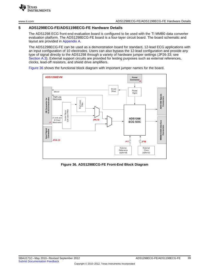
5 ADS1298ECG-FE/ADS1198ECG-FE Hardware Details
The ADS1298 ECG front-end evaluation board is configured to be used with the TI MMB0 data converterevaluation platform. The ADS1298ECG-FE board is a four-layer circuit board. The board schematic andlayout are provided in Appendix A.
The ADS1298ECG-FE can be used as a demonstration board for standard, 12-lead ECG applications withan input configuration of 10 electrodes. Users can also bypass the 12-lead configuration and provide anytype of signal directly to the ADS1298 through a variety of hardware jumper settings (JP26-33; seeSection A.3). External support circuits are provided for testing purposes such as external references,clocks, lead-off resistors, and shield drive amplifiers.
Figure 36 shows the functional block diagram with important jumper names for the board.
Figure 36. ADS1298ECG-FE Front-End Block Diagram
39SBAU171C–May 2010–Revised September 2012 ADS1298ECG-FE/ADS1198ECG-FESubmit Documentation Feedback
Copyright © 2010–2012, Texas Instruments Incorporated
ADS1298ECG-FE/ADS1198ECG-FE Hardware Details www.ti.com
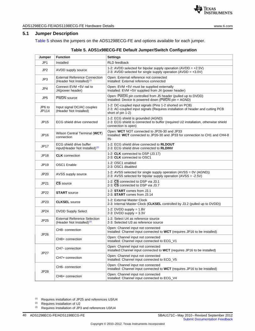
5.1 Jumper Description
Table 5 shows the jumpers on the ADS1298ECG-FE and options available for each jumper.
Table 5. ADS1x98ECG-FE Default Jumper/Switch Configuration
Jumper Function Settings
JP1 Installed RLD feedback
1-2: AVDD selected for bipolar supply operation (AVDD = +2.5V)JP2 AVDD supply source 2-3: AVDD selected for single supply operation (AVDD = +3.0V)
External Reference Connection Open: External reference not connectedJP3 (Header Not Installed) (1) Installed: External reference connected
Connect EVM +5V rail to Open: EVM +5V must be supplied externallyJP4 J4(power header) Installed: EVM +5V supplied from J4 (power header)
Open: PWDN pin controlled from J5 header (pulled up to DVDD)JP5 PWDN source Installed: Device is powered down (PWDN pin = AGND)
1-2: DC-coupled input signals (Pins 1-2 shorted on PCB)JP6 to Input signal DC/AC couples 2-3: AC-coupled input signals (Requires installation of header and cutting PCBJP114 (Header Not Installed) short of pin 1-2)
1-2: ECG shield is grounded (AGND)JP15 ECG shield drive connected 2-3: ECG shield is connected to buffer (required U2 installation, otherwise shield
connection is open)
Open: WCT NOT connected to JP26-30 and JP33Wilson Central Terminal (WCT)JP16 Installed: WCT connected to JP26-30 and JP33 for connection to CH1 and CH4-8connection IN-
ECG shield drive buffer 1-2: ECG shield drive connected to RLDOUTJP17 input(Header Not Installed) (2) 2-3: ECG shield drive connected to RLDINV
1-2: CLK connected to DSP (J3.17)JP18 CLK connection 2-3: CLK connected to OSC1
1-2: OSC1 enabledJP19 OSC1 Enable 2-3: OSC1 disabled
1-2: AVSS selected for single supply operation (AVSS = 0V (AGND))JP20 AVSS supply source 2-3: AVSS selected for bipolar supply operation (AVSS = -2.5V)
1-2: CS connected to DSP via J3.1JP21 CS source 2-3: CS connected to DSP via J3.7
1-2: START comes from J3.1JP22 START source 2-3: START comes from J3.14
1-2: External Master ClockJP23 CLKSEL source 2-3: Internal Master Clock (CLKSEL controlled by J3.2 (pulled up to DVDD))
1-2: DVDD supply = 1.8VJP24 DVDD Supply Select 2-3: DVDD supply = 3.3V
External Reference Selection 1-2: Select U4 as reference sourceJP25 (Header Not Installed) (3) 2-3: Selected U3 as reference source
Open: Channel input not connectedCH8- connection Installed: Channel input connected to WCT (requires JP16 to be installed)JP26
Open: Channel input not connectedCH8+ connection Installed: Channel input connected to ECG_V1
Open: Channel input not connectedCH7- connection Installed:Channel input connected to WCT (requires JP16 to be installed)JP27
Open: Channel input not connectedCH7+ connection Installed: Channel input connected to ECG_V5
Open: Channel input not connectedCH6- connection Installed: Channel input connected to WCT (requires JP16 to be installed)JP28
Open: Channel input not connectedCH6+ connection Installed: Channel input connected to ECG_V4
(1) Requires installation of JP25 and references U3/U4(2) Requires installation of U2(3) Requires installation of JP3 and references U3/U4
40 ADS1298ECG-FE/ADS1198ECG-FE SBAU171C–May 2010–Revised September 2012Submit Documentation Feedback
Copyright © 2010–2012, Texas Instruments Incorporated
www.ti.com ADS1298ECG-FE/ADS1198ECG-FE Hardware Details
Table 5. ADS1x98ECG-FE Default Jumper/Switch Configuration (continued)
Jumper Function Settings
Open: Channel input not connectedCH5- connection Installed: Channel input connected to WCT (requires JP16 to be installed)JP29
Open: Channel input not connectedCH5+ connection Installed: Channel input connected to ECG_V3
Open: Channel input not connectedCH4- connection Installed: Channel input connected to WCT (requires JP16 to be installed)JP30
Open: Channel input not connectedCH4+ connection Installed: Channel input connected to ECG_V2
Open: Channel input not connectedCH3- connection Installed: Channel input is connected to ECG_RAJP31
Open: Channel input not connectedCH3+ connection Installed: Channel input is connected to ECG_LL
Open: Channel input not connectedCH2- connection Installed: Channel input is connected to ECG_RAJP32
Open: Channel input not connectedCH2+ connection Installed: Channel input is connected to ECG_ LA
Open: Channel input not connectedCH1- connection Installed: Channel input connected to WCT (requires JP16 to be installed)JP33
Open: Channel input not connectedCH1+ connection Installed: Channel input connected to ECG_V6
5.2 Power Supply
The ADS1x98EVM mounts on the MMB0 EVM with connectors J2, J3 and J4. The main power supplies(+5V, +3V and +1.8V) for the front-end board are supplied by the host board, MMB0, through connectorJ4. All other power supplies needed for the front-end board are generated on board by powermanagement devices. The EVM is shipped in +3V unipolar supply configuration.
The ADS1298 can operate in a single supply with +3.0V to +5.0V analog supply (AVDD/AVSS) or bipolarmode supply (±1.5V to ±2.5V). An additional digital supply of and +1.8V to +3.0V digital supply (DVDD) isrequired for operation. The ADS1298EVM power consumption can be measured by removing the JP4jumper and JP24 jumper to connect an ammeter. By shorting JP5, the ADS1298 can be placed inpowerdown mode for low power consumption.
Test points TP5, TP6, TP7, TP8, TP9, TP10, and TP14 are provided to verify the power supplies voltagesare correct. The test points and voltages are shown in Table 6.
Table 6. Power-Supply Test Points
Test Point Voltage
TP7 +5.0V
TP9 +1.8V
TP10 +3.3V
TP5 +3.0V
TP13 +2.5V
TP6 –2.5V
TP8 GND
The front-end board must be properly configured in order to achieve the various power-supply schemes.The default power-supply setting for the ADS1298ECG-FE is a bipolar analog supply of ±2.5V and DVDDof either +3V or +1.8V. Table 7 shows the board and component configurations for each analog power-supply scheme and Table 8 shows the board configurations for the digital supply.
41SBAU171C–May 2010–Revised September 2012 ADS1298ECG-FE/ADS1198ECG-FESubmit Documentation Feedback
Copyright © 2010–2012, Texas Instruments Incorporated
ADS1298ECG-FE/ADS1198ECG-FE Hardware Details www.ti.com
Table 7. Analog Supply Configurations (AVDD/AVSS)
Unipolar Analog Supply Bipolar Analog Supply
AVDD/AVSS 3V 5V ±1.5V ±2.5V
JP20 1-2 1-2 2-3 2-3
JP2 2-3 2-3 1-2 1-2
U7 TPS73230 TPS73250 Don't Care Don't Care
U9 Don't Care Don't Care TPS73201 TPS73201
U8 Don't Care Don't Care TPS72301 TPS72301
R52 Don't Care Don't Care 21kΩ 47.5kΩR53 Don't Care Don't Care 78.7kΩ 43kΩR56 Don't Care Don't Care 23.3kΩ 49.9kΩR57 Don't Care Don't Care 95.3kΩ 46.4kΩ
C87, C67, C62 Not Installed Not Installed Not Installed Not Installed
Table 8. Digital Supply Configurations (DVDD/DGND)
DVDD +3.0V +1.8V
JP24 1-2 2-3
5.3 Clock
The ADS1298 has an on-chip oscillator circuit that generates a 2.048MHz clock (nominal). This clock canvary by ±5% over temperature. For applications that require higher accuracy, the ADS1298 also acceptsan external clock signal. The ADS1298ECG-FE provides an option to test both internal and external clockconfigurations. For the external signal, circuitry is available to generate the external clock from an on-board oscillator or from an externally connected source.
The external oscillator included on the EVM is powered from DVDD, the same supply as the ADS1298.Care must be taken to ensure that the externally supplied clock oscillator can operate either with +1.8V or+3.0V, depending on the DVDD supply configuration. Table 9 shows the jumper settings for the threeoptions for the ADS1298 clocks.
Table 9. CLK Jumper Options
ADS1298 Clock Internal Clock External OSC Clock External Clock
JP18 Not Installed 2-3 1-2
1-2 (Disable)JP19 Don't Care Don't Care
2-3 (Enable)
A 2.048MHz oscillator installed on the EVM for +3V DVDD operation is FXO-HC735-2.048MHz. Ifoperation at +1.8V DVDD is desired, the oscillator will need to be replaced. SiT8002AC-34-18E-2.048 is apossible oscillator for +1.8V DVDD operation. The EVM is shipped with the external oscillator enabled.
5.4 Reference
The ADS1298 has an on-chip internal reference circuit that provides reference voltages to the device.Alternatively, the internal reference can be powered down and VREFP can be applied externally. Thisconfiguration is achieved with the external reference generators (U3 and U4) and driver buffer. NOTE: U3,U4, and driver buffer are not installed. The externally provided reference voltage can be set to either4.096V or 2.5V, depending on the analog supply voltage. Measure TP3 to make sure the externalreference is correct. The settings for the external reference is described in Table 10.
42 ADS1298ECG-FE/ADS1198ECG-FE SBAU171C–May 2010–Revised September 2012Submit Documentation Feedback
Copyright © 2010–2012, Texas Instruments Incorporated
www.ti.com ADS1298ECG-FE/ADS1198ECG-FE Hardware Details
Table 10. External Reference Jumper Options
Internal Reference External Reference
ADS1298 Reference VREF = 2.5V VREFP = 4.096V VREFP = 2.5V
JP25 Don't Care 2-3 1-2
JP3 Not Installed Installed Installed
The software uses the VREF value from the Reference Voltage control (CONFIG3 register) inSection 3.4.2.1) to calculate the input-referred voltage value for all the tests. The default value is 2.5V. Ifthe user is using an alternative value, the control must be updated to display the collected data to theproper scale.
5.5 Analog Output Signals
Several output signals from the ADS1298 are provided on the J5 header. Table 11 lists the various testsignals and their location on the header. The PACEOUT pins can also be used as an auxiliary differentialinput channel. Alternatively with appropriate user configuration, these pins may provide PACE detectionfor use with external PACE detection circuitry (see PACE Detect Register in Section 3.4.4).
Table 11. Test Signals
Signal J5 Pin Number Signal
PACEOUT2 1 2 PACEOUT1
NOT CONNECTED 3 4 NOT CONNECTED
PWDNB 5 6 GPIO4
DAISY_IN 7 8 GPIO3
GND 9 10 NOT CONNECTED
5.6 Digital Signals
The ADS1298 digital signals (including SPI interface signals, some GPIO signals, and some of the controlsignals) are available at connector J3. These signals are used to interface to the MMB0 board DSP. Thepinout for this connector is given in Table 12.
Table 12. Serial Interface Pinout
Signal J3 Pin Number Signal
START/CS 1 2 CLKSEL
CLK 3 4 GND
NC 5 6 GPIO1
CS 7 8 RESETB
NC 9 10 GND
DIN 11 12 GPIO2
DOUT 13 14 NC/START
DRDYB 15 16 NC
NC 17 18 GND
NC 19 20 NC
5.7 Analog Input Signals
The ADS1298ECG-FE provides users the option to feed in standard ECG signals from a patient simulatorto the DB15 connector (J1), or to feed inputs from any arbitrary signal source directly to the ADS1298.
43SBAU171C–May 2010–Revised September 2012 ADS1298ECG-FE/ADS1198ECG-FESubmit Documentation Feedback
Copyright © 2010–2012, Texas Instruments Incorporated
ADS1298ECG-FE/ADS1198ECG-FE Hardware Details www.ti.com
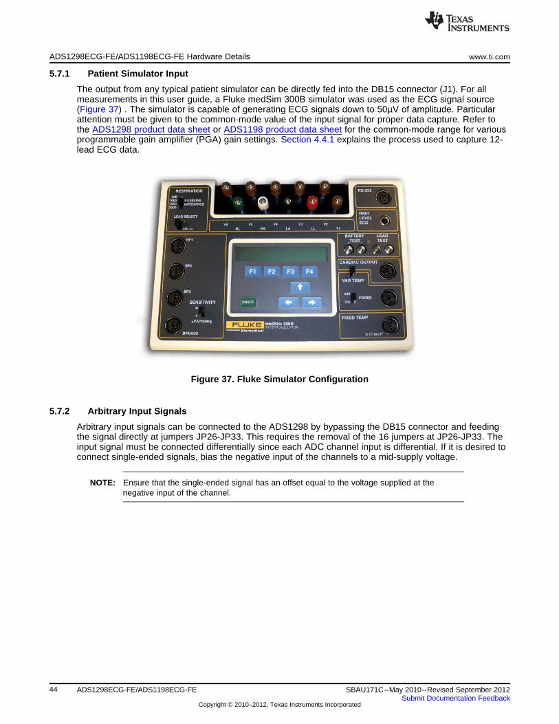
5.7.1 Patient Simulator Input
The output from any typical patient simulator can be directly fed into the DB15 connector (J1). For allmeasurements in this user guide, a Fluke medSim 300B simulator was used as the ECG signal source(Figure 37) . The simulator is capable of generating ECG signals down to 50µV of amplitude. Particularattention must be given to the common-mode value of the input signal for proper data capture. Refer tothe ADS1298 product data sheet or ADS1198 product data sheet for the common-mode range for variousprogrammable gain amplifier (PGA) gain settings. Section 4.4.1 explains the process used to capture 12-lead ECG data.
Figure 37. Fluke Simulator Configuration
5.7.2 Arbitrary Input Signals
Arbitrary input signals can be connected to the ADS1298 by bypassing the DB15 connector and feedingthe signal directly at jumpers JP26-JP33. This requires the removal of the 16 jumpers at JP26-JP33. Theinput signal must be connected differentially since each ADC channel input is differential. If it is desired toconnect single-ended signals, bias the negative input of the channels to a mid-supply voltage.
NOTE: Ensure that the single-ended signal has an offset equal to the voltage supplied at thenegative input of the channel.
44 ADS1298ECG-FE/ADS1198ECG-FE SBAU171C–May 2010–Revised September 2012Submit Documentation Feedback
Copyright © 2010–2012, Texas Instruments Incorporated

www.ti.com
Appendix A Schematics, BOM, Layout, and ECG Cable Details
This section contains the complete bill of materials, printed circuit board (PCB) layouts, and schematicdiagrams for the ADS1x98ECG-FE.
NOTE: Board layouts are not to scale. These are intended to show how the board is laid out; theyare not intended to be used for manufacturing ADS1298ECG-FE PCBs.
A.1 ADS1x98ECG-FE Front-End Board Schematics
The ADS1x98ECG-FE schematic is appended to this document.
45SBAU171C–May 2010–Revised September 2012 Schematics, BOM, Layout, and ECG Cable DetailsSubmit Documentation Feedback
Copyright © 2010–2012, Texas Instruments Incorporated
Bill of Materials www.ti.com
A.2 Bill of Materials
Table 13 lists the bill of materials for the ADS1x98ECG-FE.
Table 13. Bill of Materials: ADS1x98ECG-FE
Count RefDes Description Size Part Number MFR
1 NA Printed wiring board 6514709 TI
15 C1, C2, C3, C4, C5, Capacitor, ceramic 1µF 25V 10% X5R 0603 GRM188R61E105KA12D MurataC6, C11, C17, C47,
C48, C49, C52, C58,C76, C77
0 C7, C8, C15, C19, Not installedC21, C22, C25, C27,C34, C36, C38, C40,C41, C42, C43, C44,C56, C62, C67, C78,C79, C81, C83, C85,
C87, C89
1 C9 Capacitor, ceramic 22µF 6.3V 10% X5R 0805 JMK212BJ226KG-T Taiyo Yuden
11 C10, C45, C46, C50, Capacitor, ceramic 10µF 10V 10% X5R 0805 GRM219R61A106KE44D MurataC51, C54, C55, C60,
C61, C65, C66
10 C12, C13, C14, C16, Capacitor, ceramic 0.1µF 50V 10% X7R 0603 GRM188R71H104KA93D MurataC18, C57, C69, C70,
C94, C95
1 C20 Capacitor, ceramic 10nF 50V 10% X7R 0603 GRM188R71H103KA01D Murata
20 C23, C24, C26, C28, Capacitor, ceramic 47pF 50V 5% C0G 0603 GRM1885C1H470JA01D MurataC29, C30, C31, C32,C72, C73, C74, C75,C80, C82, C84, C86,C88, C91, C92, C93
0 C33, C35, C37 Not installed
0 C39 Not installed
4 C53, C59, C63, C64 Capacitor, ceramic 2.2µF 6.3V 10% X5R 0603 GRM185R60J225KE26D Murata
2 C68, C71 Capacitor, ceramic 100µF 10V 20% X5R 1210 LMK325BJ107MM-T Taiyo Yuden
1 C90 Capacitor, ceramic 1000pF 50V 5% X7R 0603 C1608X7R1H102J TDK
0 D1 - D10 Not installed
1 J1 Connector, DSUB Rcpt 15-position R/A PCB SLD D15S13A4GV00LF FCI
2 J2, J3 10x2x0.1 female (installed from bottom side) SSW-110-21-FM-D Samtec
1 J4 5x2x0.1 female (installed from bottom side) SSW-105-21-FM-D Samtec
0 J5 Not installed
4 JP1, JP4, JP5, JP16 2-position jumper 0 .1" spacing TSW-102-07-T-S Samtec
0 JP3 Not installed
0 JP6, JP7, JP8, JP9, Not installedJP10, JP11, JP12,JP13, JP14, JP17,
JP25
9 JP2, JP15, JP18, 3-position jumper 0.1" spacing TSW-103-07-T-S SamtecJP19, JP20, JP21,JP22, JP23, JP24
8 JP26, JP27, JP28, 2x2x0.1, 2-pin dual row header TSW-102-07-T-D SamtecJP29, JP30, JP31,
JP32, JP33
5 L1 - L5 Ferrite bead 470Ω 0805 BK2125HM471-T Taiyo Yuden
0 R1, R4, R5, R11, Not installedR12, R15, R16, R19,R20, R23, R24, R27,R28, R31, R32, R35,R36, R41, R42, R45 -R51, R54, R55, R58 -R66, R68, R69, R70
0 R2 Not installed
5 R3, R71, R72, R73, Resistor, 0.0Ω 1/10W 5% SMD 0603 RC0603JR-070RL YageoR74
46 Schematics, BOM, Layout, and ECG Cable Details SBAU171C–May 2010–Revised September 2012Submit Documentation Feedback
Copyright © 2010–2012, Texas Instruments Incorporated
www.ti.com Bill of Materials
Table 13. Bill of Materials: ADS1x98ECG-FE (continued)
Count RefDes Description Size Part Number MFR
14 R6, R7, R10, R14, Resistor, 10.0kΩ 1/10W 1% SMD 0603 RC0603FR-0710KL YageoR18, R22, R26, R30,R34, R38, R40, R44,
R67, R75
1 R8 Resistor, 392kΩ 1/10W 1% SMD 0603 RC0603FR-07392KL Yageo
10 R9, R13, R17, R21, Resistor, 22.1kΩ 1/10W 1% SMD 0603 RC0603FR-0722K1L YageoR25, R29, R33, R37,
R39, R43
1 R52 Resistor, 47.5kΩ 1/10W 1% SMD 0603 RC0603FR-0747K5L Yageo
1 R53 Resistor, 43.2kΩ 1/10W 1% SMD 0603 RC0603FR-0743K2L Yageo
1 R56 Resistor, 49.9kΩ 1/10W 1% SMD 0603 RC0603FR-0749K9L Yageo
1 R57 Resistor, 46.4kΩ 1/10W 1% SMD 0603 RC0603FR-0746K4L Yageo
5 TP1, TP2, TP8, TP11, Test point PC Mini .040"D BLACK 5001 KeystoneTP12
8 TP3, TP4, TP5, TP6, Test point PC Mini .040"D RED 5000 KeystoneTP7, TP9, TP10,
TP13
1 U1 (1) IC ADC 24BIT SPI 32KSPS 64TQFP ADS1298IPAG TI
IC ADC 16BIT SPI 8KSPS 64TQFP ADS1198IPAG TI
0 U2 Not Installed
0 U3, U4, U5 Not installed
1 U6 IC UNREG CHRG PUMP V INV SOT23-5 TPS60403DBVR TI
1 U7 IC LDO REG 250MA 3.0V SOT23-5 TPS73230DBVT TI
1 U8 IC LDO REG NEG 200MA ADJ SOT23-5 TPS72301DBVT TI
1 U9 IC LDO REG 250MA ADJ-V SOT23-5 TPS73201DBV TI
1 U10 IC EEPROM 256KBIT 400KHZ 8TSSOP 24AA256-I/ST Microchip
1 OSC1 OSC 2.0480 MHz 3.3V HCMOS SMT FXO-HC735-2.048MHZ Fox
(1) Installed device is determined by Installed Device checkbox located near lower left corner of the board.
47SBAU171C–May 2010–Revised September 2012 Schematics, BOM, Layout, and ECG Cable DetailsSubmit Documentation Feedback
Copyright © 2010–2012, Texas Instruments Incorporated

Printed Circuit Board Layout www.ti.com
A.3 Printed Circuit Board Layout
Figure 38 through Figure 43 show the ADS1x98ECG-FE PCB layouts.
Figure 38. Top Component Placement Figure 39. Top Layer
Figure 40. Bottom Component Placement Figure 41. Bottom Layer
48 Schematics, BOM, Layout, and ECG Cable Details SBAU171C–May 2010–Revised September 2012Submit Documentation Feedback
Copyright © 2010–2012, Texas Instruments Incorporated
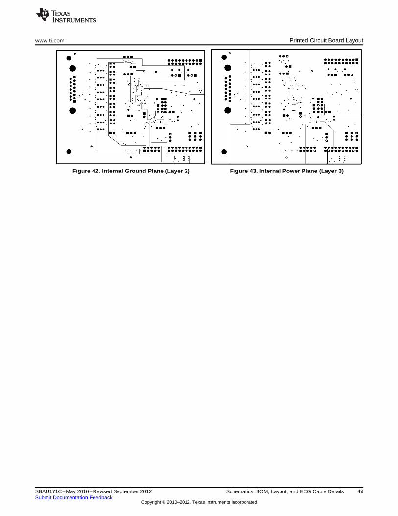
www.ti.com Printed Circuit Board Layout
Figure 42. Internal Ground Plane (Layer 2) Figure 43. Internal Power Plane (Layer 3)
49SBAU171C–May 2010–Revised September 2012 Schematics, BOM, Layout, and ECG Cable DetailsSubmit Documentation Feedback
Copyright © 2010–2012, Texas Instruments Incorporated
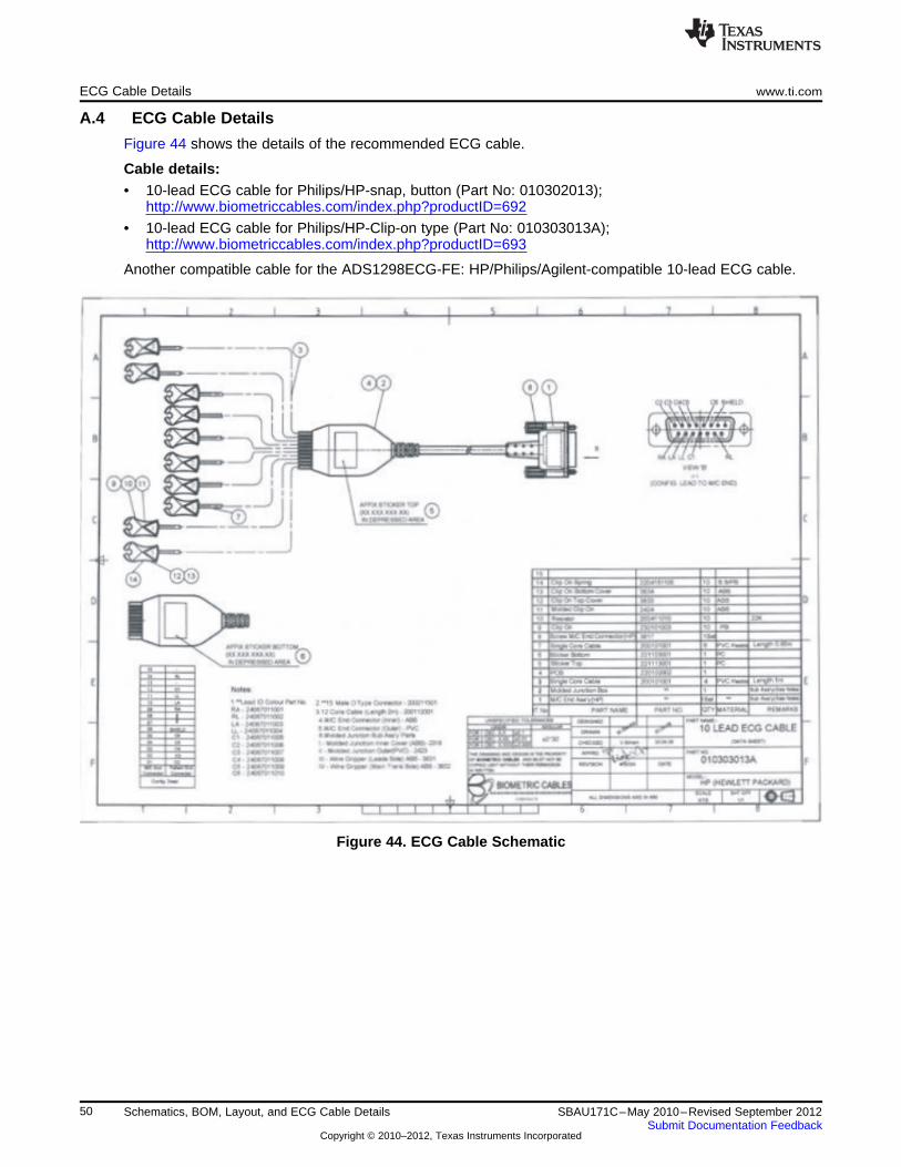
ECG Cable Details www.ti.com
A.4 ECG Cable Details
Figure 44 shows the details of the recommended ECG cable.
Cable details:• 10-lead ECG cable for Philips/HP-snap, button (Part No: 010302013);
http://www.biometriccables.com/index.php?productID=692
• 10-lead ECG cable for Philips/HP-Clip-on type (Part No: 010303013A);http://www.biometriccables.com/index.php?productID=693
Another compatible cable for the ADS1298ECG-FE: HP/Philips/Agilent-compatible 10-lead ECG cable.
Figure 44. ECG Cable Schematic
50 Schematics, BOM, Layout, and ECG Cable Details SBAU171C–May 2010–Revised September 2012Submit Documentation Feedback
Copyright © 2010–2012, Texas Instruments Incorporated
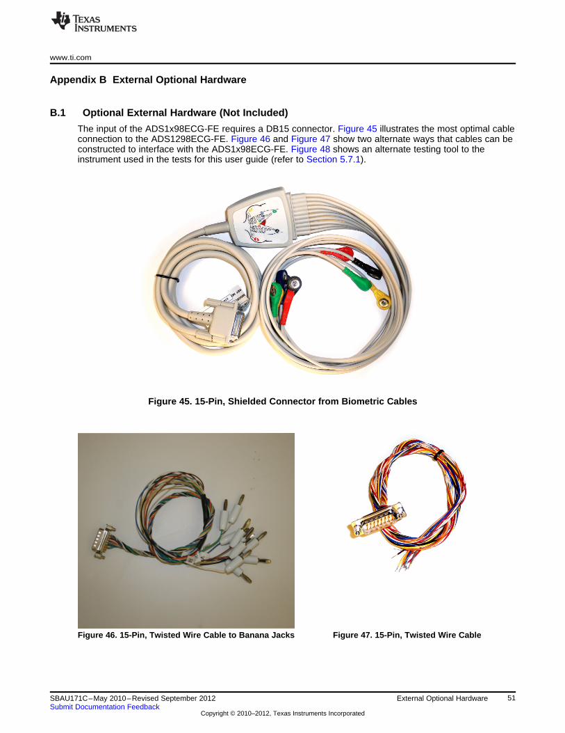
www.ti.com
Appendix B External Optional Hardware
B.1 Optional External Hardware (Not Included)
The input of the ADS1x98ECG-FE requires a DB15 connector. Figure 45 illustrates the most optimal cableconnection to the ADS1298ECG-FE. Figure 46 and Figure 47 show two alternate ways that cables can beconstructed to interface with the ADS1x98ECG-FE. Figure 48 shows an alternate testing tool to theinstrument used in the tests for this user guide (refer to Section 5.7.1).
Figure 45. 15-Pin, Shielded Connector from Biometric Cables
Figure 46. 15-Pin, Twisted Wire Cable to Banana Jacks Figure 47. 15-Pin, Twisted Wire Cable
51SBAU171C–May 2010–Revised September 2012 External Optional HardwareSubmit Documentation Feedback
Copyright © 2010–2012, Texas Instruments Incorporated
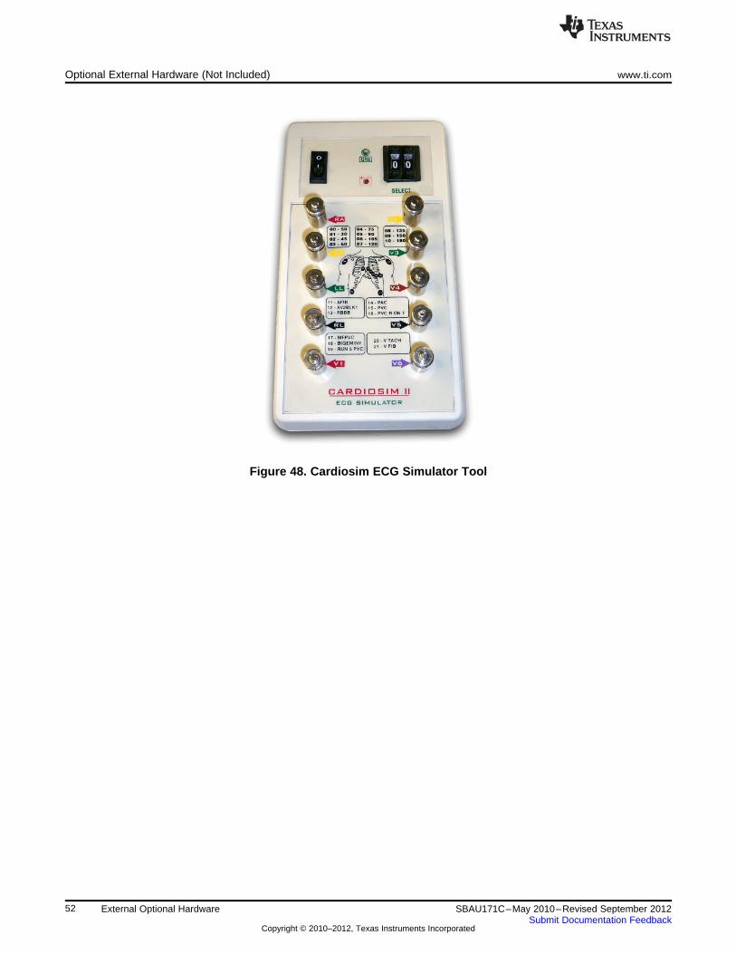
Optional External Hardware (Not Included) www.ti.com
Figure 48. Cardiosim ECG Simulator Tool
52 External Optional Hardware SBAU171C–May 2010–Revised September 2012Submit Documentation Feedback
Copyright © 2010–2012, Texas Instruments Incorporated

www.ti.com ADS1x98ECG-FE Power-Supply Recommendations
B.2 ADS1x98ECG-FE Power-Supply Recommendations
Figure 49 shows a +6V power-supply cable (not provided in the EVM kit) connected to a battery pack withfour 1.5V batteries connected in series. Connecting to a wall-powered source (provided in the EVM kit)makes the ADS1x98ECG-FE more susceptible to 50Hz/60Hz noise pickup; therefore, for bestperformance, it is recommended to power the ADS1x98ECG-FE with a battery source. This configurationminimizes the amount of noise pickup seen at the digitized output of the ADS1298.
Figure 49. Recommended Power Supply for ADS1x98ECG-FE
53SBAU171C–May 2010–Revised September 2012 External Optional HardwareSubmit Documentation Feedback
Copyright © 2010–2012, Texas Instruments Incorporated
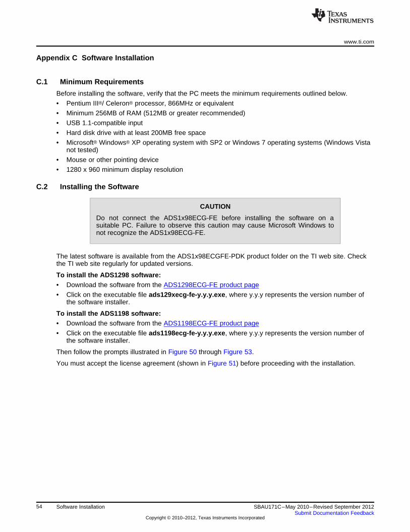
www.ti.com
Appendix C Software Installation
C.1 Minimum Requirements
Before installing the software, verify that the PC meets the minimum requirements outlined below.
• Pentium III®/ Celeron® processor, 866MHz or equivalent
• Minimum 256MB of RAM (512MB or greater recommended)
• USB 1.1-compatible input
• Hard disk drive with at least 200MB free space
• Microsoft® Windows® XP operating system with SP2 or Windows 7 operating systems (Windows Vistanot tested)
• Mouse or other pointing device
• 1280 x 960 minimum display resolution
C.2 Installing the Software
CAUTION
Do not connect the ADS1x98ECG-FE before installing the software on asuitable PC. Failure to observe this caution may cause Microsoft Windows tonot recognize the ADS1x98ECG-FE.
The latest software is available from the ADS1x98ECGFE-PDK product folder on the TI web site. Checkthe TI web site regularly for updated versions.
To install the ADS1298 software:• Download the software from the ADS1298ECG-FE product page
• Click on the executable file ads129xecg-fe-y.y.y.exe, where y.y.y represents the version number ofthe software installer.
To install the ADS1198 software:• Download the software from the ADS1198ECG-FE product page
• Click on the executable file ads1198ecg-fe-y.y.y.exe, where y.y.y represents the version number ofthe software installer.
Then follow the prompts illustrated in Figure 50 through Figure 53.
You must accept the license agreement (shown in Figure 51) before proceeding with the installation.
54 Software Installation SBAU171C–May 2010–Revised September 2012Submit Documentation Feedback
Copyright © 2010–2012, Texas Instruments Incorporated
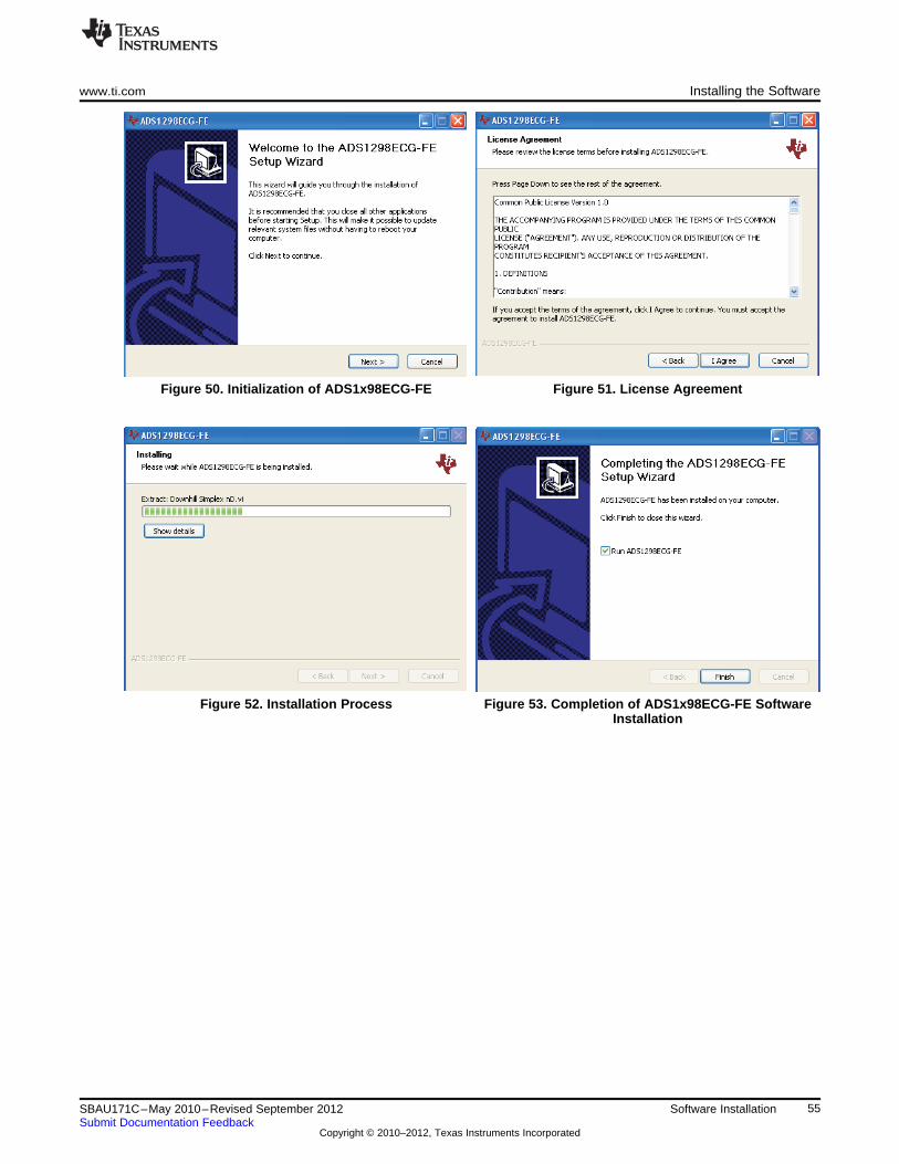
www.ti.com Installing the Software
Figure 50. Initialization of ADS1x98ECG-FE Figure 51. License Agreement
Figure 52. Installation Process Figure 53. Completion of ADS1x98ECG-FE SoftwareInstallation
55SBAU171C–May 2010–Revised September 2012 Software InstallationSubmit Documentation Feedback
Copyright © 2010–2012, Texas Instruments Incorporated
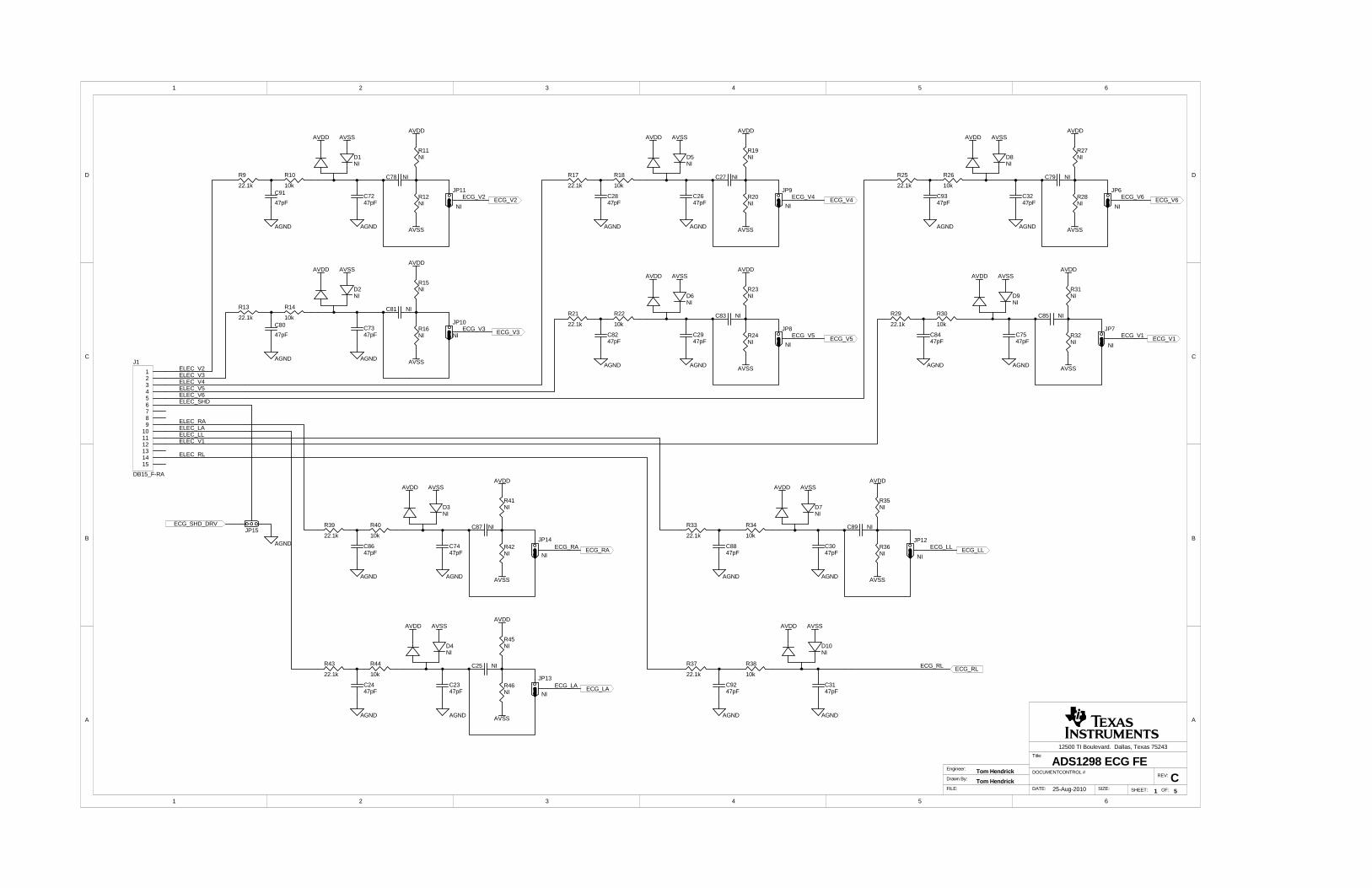
1 2 3 4 5 6
A
B
C
D
654321
D
C
B
A
FILE:
Drawn By:
Engineer:
ti12500 TI Boulevard. Dallas, Texas 75243
Title:
SHEET: OF:SIZE:DATE:
REV:
25-Aug-2010
DOCUMENTCONTROL #
123456789
1011
1413
15
12
J1
DB15_F-RA
ECG_LL
ECG_LA
ECG_RA
ECG_RL
ECG_V1
ECG_V2
ECG_V3
ECG_V4
ECG_V5
ECG_V6
AVDD AVSS
R10
10k
R9
22.1k
C7247pF
AVDD AVSS
R14
10k
R13
22.1k
C7347pF
AVDD AVSS
R40
10k
R39
22.1k
C7447pF
AVDD AVSS
R44
10k
R43
22.1k
C2347pF
AVDD AVSS
R18
10k
R17
22.1k
C2647pF
AVDD AVSS
R22
10k
R21
22.1k
C2947pF
AVDD AVSS
R34
10k
R33
22.1k
C3047pF
AVDD AVSS
R38
10k
R37
22.1k
C3147pF
AVDD AVSS
R26
10k
R25
22.1k
C3247pF
AVDD AVSS
R30
10k
R29
22.1k
C7547pF
ELEC_V2ELEC_V3ELEC_V4ELEC_V5ELEC_V6
ELEC_RAELEC_LAELEC_LLELEC_V1
ELEC_RL
JP15
ELEC_SHD
ECG_V2
ECG_V3
ECG_V4
ECG_V5
ECG_V6
ECG_LA
ECG_RA ECG_LL
ECG_RL
ECG_V1
ECG_SHD_DRV
1 5
C85 NI
AVSS
AVDD
R31NI
R32NI
C89 NI
AVSS
AVDD
R35NI
R36NI
C79 NI
AVSS
AVDD
R27NI
R28NI
C87 NI
AVSS
AVDD
R41NI
R42NI
C78 NI
AVSS
AVDD
R11NI
R12NI
C81 NI
AVSS
AVDD
R15NI
R16NI
C25 NI
AVSS
AVDD
R45NI
R46NI
C27 NI
AVSS
AVDD
R19NI
R20NI
C83 NI
AVSS
AVDD
R23NI
R24NI
JP11
NI
JP10
NI
JP14
NI
JP13
NI
JP12
NI
JP6
NI
JP9
NI
JP7
NI
JP8
NI
CTom Hendrick
Tom Hendrick
C91
47pF
C80
47pF
C8647pF
C2447pF
C9247pF
C8847pF
C2847pF
C8247pF
C8447pF
C9347pF
AGND AGND
AGND AGND
AGND
AGND AGND
AGND AGND
AGND AGND
AGNDAGND
AGND AGND
AGND AGND
AGND AGND
AGND AGND
ADS1298 ECG FE
D1NI
D2NI
D3NI
D4NI
D5NI
D6NI
D7NI
D10NI
D8NI
D9NI

1 2 3 4 5 6
A
B
C
D
654321
D
C
B
A
FILE:
Drawn By:
Engineer:
ti12500 TI Boulevard. Dallas, Texas 75243
Title:
SHEET: OF:SIZE:DATE:
REV:
25-Aug-2010
DOCUMENTCONTROL #
GPIO1/RESET
/PWDN
PACEOUT1PACEOUT2
C4
1uF C9
22uF
C10
10uF
C1
1uF
C2
1uF
C3
1uF
C20
0.01uF
R3 0
R5 NI
R1
NI
VC
AP
4
VB
G VC
AP
2
C13
0.1uF
C14
0.1uF
C12
0.1uF
C5
1uF
C8
NI
C16
0.1uF
C6
1uF
C15
NI
C7
NI
C19
NI
VREFP
RLD
INV
RLD
OU
TR
LDIN
C33
NI
R2
NI
VDD4
GND 2Output3
E/D 1
OSC1
HC735-2.048MHZ
AVDD
AVDDAVDD
AVSS
AVSS
AVSS
JP16
ECG_RL
VREFP
AVSS
AVSSAVSS
AVDD
AVDD
DVDD
C11
1uF
JP19
DVDD
CLKSEL
SPI_DRDY
SPI_OUTGPIO2
SPI_CLKSPI_CS
SPI_START
ECG ADC Frontend
AVDD
SPI_IN
JP1
GPIO1
R610K
R710K
DVDD
ECG_RL
C22 NI
C21 NI
AVSS
AVDD
R4
NIECG_SHD_DRV ECG_SHD_DRVJP17
NI
DVDD
VCAP3
/RESET
/PWDN
SPI_DRDYGPIO4SPI_OUTGPIO2GPIO3SPI_CLKSPI_CS
SPI_STARTSPI_IN
CLKSEL
CLK
AVSS
C761uF
AVSS AVSS
C771uF
AVSS
JP5
C17
1uF
C18
0.1uF
AVDD
1
2
34
5
U2NI
C90
100pF
AVSS
ECG_LL
ECG_LAECG_RA
ECG_V1
ECG_V2
ECG_V3
ECG_V4
ECG_V5
ECG_V6
R59NI
R60NI
R61NI
R62NI
R63NI
R64NI
R65NI
R66NI
AVDD
R58NI
AVSS
ECG_V2
ECG_V3
ECG_V4
ECG_V5
ECG_V6
ECG_LAECG_RAECG_LL
ECG_V1
PACEOUT2PACEOUT1
PACEOUT2PACEOUT1
/PWDN
DAISY_IN
GPIO3
GPIO4
DAISY_IN
GPIO3GPIO4
DAISY_IN
12345678910
J5
NI
JP18
EXT_CLKEXT_CLK
WCT
TP11 TP12TP1 TP2
2 5
CTom Hendrick
Tom Hendrick
AGND
AGND
AGND
AGND
AGND
AGND AGND
AGND
AGND
AGND
AGND
AGND
AGND
ADS1298 ECG FE
R8392K
TP3
1 23 4
JP26
1 23 4
JP33
1 23 4
JP27
1 23 4
JP28
1 23 4
JP29
1 23 4
JP30
1 23 4
JP31
1 23 4
JP32
IN8N1
IN8P2
IN7N3
IN7P4
IN6N5
IN6P6
IN5N7
IN5P8
IN4N9
IN4P10
IN3N11
IN3P12
IN2N13
IN2P14
IN1N15
IN1P16
PA
CE
_OU
T2
18
PA
CE
_OU
T1
17
VR
EF
P24
VC
AP
426
AV
SS
20
RE
SV
3/N
C29
VR
EF
N25
RE
SV
2/N
C27
/PW
DN
35
VC
AP
128
GP
IO1
42
DA
ISY
_IN
41
VC
AP
230
/RE
SE
T36
DGND 33DIN 34START 38CLK 37/CS 39SCLK 40GPIO3 45GPIO2 44DOUT 43GPIO4 46/DRDY 47DVDD 48DGND 51AVSS 32DVDD 50DGND 49CLKSEL 52
AV
SS
153
AV
DD
154
VC
AP
355
AV
DD
59A
VD
D56
AV
SS
23
AV
SS
57A
VS
S58
AV
DD
19A
VD
D21
RLD
IN62
RLD
INV
61
RLD
OU
T63
RESV131
AV
DD
22
RLD
RE
F60
WCT64
U1ADS1198
C95
0.1uF
R75
10K
DVDD

1 2 3 4 5 6
A
B
C
D
654321
D
C
B
A
FILE:
Drawn By:
Engineer:
ti12500 TI Boulevard. Dallas, Texas 75243
Title:
SHEET: OF:SIZE:DATE:
REV:
25-Aug-2010
DOCUMENTCONTROL #
VIN2
GND4
OUT 6
TRIM 5
TEMP3
N/C1 N/C
7
N/C
8 U4NI
R51
NIVREFP
R50 NI
C40 NI
3
26
74
8
U5
NI
External Reference Drivers
C36
NI
AVDD
AVDD
AVSS
AVSS
R47
NI
C37
NI
C38NI
C39NI
R48
NI
C42 NI
C41 NI
R49NI
JP3
NI
External Reference
C44
NI
VIN2
GND4
OUT 6
TRIM 5
TEMP3
N/C1 N/C
7
N/C
8 U3NI
C34
NI
AVDD
AVSS
C43
NI
JP25
NI
C35
NI
AVSS
AVSS
NOT INSTALLED
3 5
CTom Hendrick
Tom Hendrick
AGND
AGND
ADS1298 ECG FE
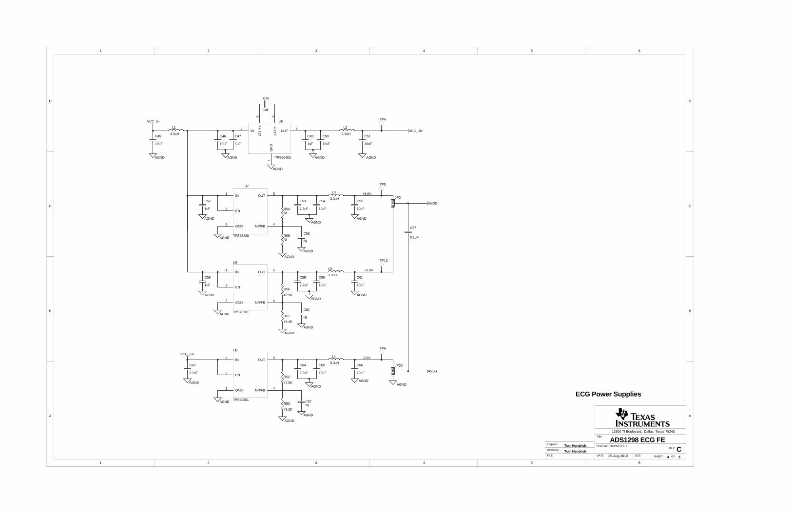
1 2 3 4 5 6
A
B
C
D
654321
D
C
B
A
FILE:
Drawn By:
Engineer:
ti12500 TI Boulevard. Dallas, Texas 75243
Title:
SHEET: OF:SIZE:DATE:
REV:
25-Aug-2010
DOCUMENTCONTROL #
VCC_5v
AVDD
VCC_-5v
CF
LY-
3G
ND
4
CF
LY+
5
IN2 OUT 1
U6
TPS60403
C45
10uF
C46
10uF
C47
1uF
L1
3.3uH
L2
3.3uHC50
10uF
C49
1uF
C51
10uF
TP4
C52
1uF
C48
1uF
C56
NI
C53
2.2uF
L3
3.3uHC55
10uF
TP5
VCC_-5v
AVSS
C63
2.2uF
C67NI
C64
2.2uF
L4
3.3uHC66
10uF
TP6
C54
10uF
C65
10uF
ECG Power Supplies
C57
0.1uF
R52
47.5K
R53
43.2K
JP20
JP2
EN3
NR/FB 4
OUT 5
GND2
IN1
U7
TPS73230
R54NI
R55NI
C62
NI
C59
2.2uF
L5
3.3uHC61
10uF
C60
10uFEN3
NR/FB 4
OUT 5
GND2
IN1
U9
TPS73201
R56
49.9K
R57
46.4K
C58
1uF
TP13
EN3
NR/FB 4
OUT 5IN2
GND1
U8
TPS72301
4 5
CTom Hendrick
Tom Hendrick
AGND AGND
AGND
AGND AGND
AGND
AGND
AGND
AGNDAGND
AGND
+3.0V
-2.5V
+2.5V
AGNDAGND
AGND
AGND
AGND
AGND
AGND
AGND
AGND
AGND
AGND
AGNDAGND
ADS1298 ECG FE
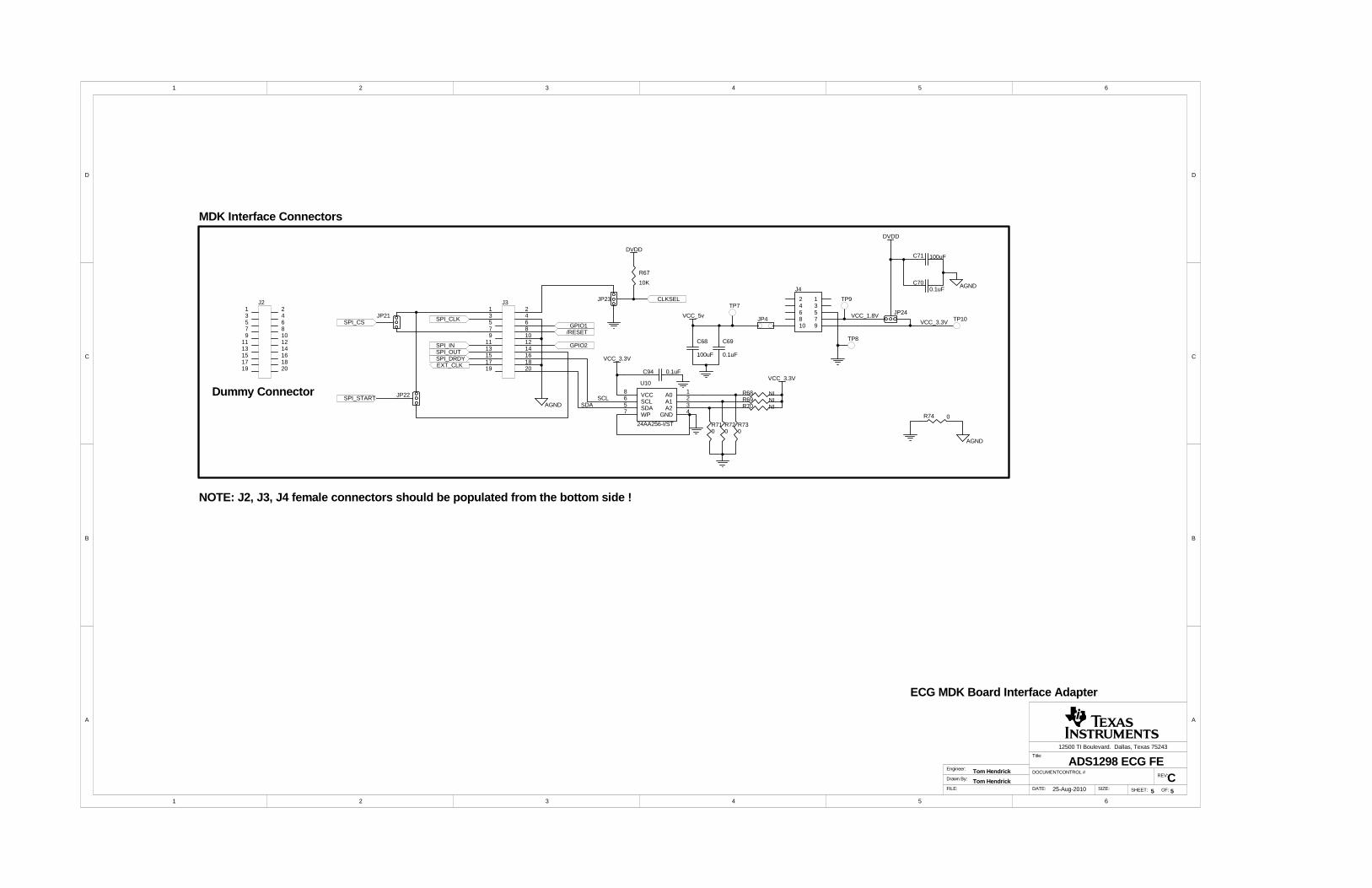
1 2 3 4 5 6
A
B
C
D
654321
D
C
B
A
FILE:
Drawn By:
Engineer:
ti12500 TI Boulevard. Dallas, Texas 75243
Title:
SHEET: OF:SIZE:DATE:
REV:
25-Aug-2010
DOCUMENTCONTROL #
1 23 45 67 89 10
11 1213 1415 1617 1819 20
J31 23 45 67 89 10
11 1213 1415 1617 1819 20
J2
ECG MDK Board Interface Adapter
VCC_5v
DVDD
12345678910
J4
TP8
TP10
TP9TP7
C700.1uF
C69
0.1uF
C71 100uF
C68
100uF
CLKSEL
SPI_DRDYSPI_OUT
GPIO2
SPI_CLKSPI_CS
SPI_START
SPI_IN
GPIO1
MDK Interface Connectors
Dummy Connector
JP4
/RESET
JP24JP21
JP22
NOTE: J2, J3, J4 female connectors should be populated from the bottom side !
EXT_CLK
R67
10K
JP23
DVDD
5 5
CTom Hendrick
Tom Hendrick
AGND
AGND
AGND
VCC_1.8VVCC_3.3V
R74 0
ADS1298 ECG FE
A0 1
A1 2
GND 4SDA5 SCL6
WP7
VCC8
A2 3
U10
24AA256-I/ST
C94 0.1uFVCC_3.3V
R68 NI
VCC_3.3V
R69 NIR70 NI
R710
R720
R730
SCLSDA

EVALUATION BOARD/KIT/MODULE (EVM) ADDITIONAL TERMS
Texas Instruments (TI) provides the enclosed Evaluation Board/Kit/Module (EVM) under the following conditions:
The user assumes all responsibility and liability for proper and safe handling of the goods. Further, the user indemnifies TI from all claimsarising from the handling or use of the goods.
Should this evaluation board/kit not meet the specifications indicated in the User’s Guide, the board/kit may be returned within 30 days fromthe date of delivery for a full refund. THE FOREGOING LIMITED WARRANTY IS THE EXCLUSIVE WARRANTY MADE BY SELLER TOBUYER AND IS IN LIEU OF ALL OTHER WARRANTIES, EXPRESSED, IMPLIED, OR STATUTORY, INCLUDING ANY WARRANTY OFMERCHANTABILITY OR FITNESS FOR ANY PARTICULAR PURPOSE. EXCEPT TO THE EXTENT OF THE INDEMNITY SET FORTHABOVE, NEITHER PARTY SHALL BE LIABLE TO THE OTHER FOR ANY INDIRECT, SPECIAL, INCIDENTAL, OR CONSEQUENTIALDAMAGES.
Please read the User's Guide and, specifically, the Warnings and Restrictions notice in the User's Guide prior to handling the product. Thisnotice contains important safety information about temperatures and voltages. For additional information on TI's environmental and/or safetyprograms, please visit www.ti.com/esh or contact TI.
No license is granted under any patent right or other intellectual property right of TI covering or relating to any machine, process, orcombination in which such TI products or services might be or are used. TI currently deals with a variety of customers for products, andtherefore our arrangement with the user is not exclusive. TI assumes no liability for applications assistance, customer product design,software performance, or infringement of patents or services described herein.
REGULATORY COMPLIANCE INFORMATION
As noted in the EVM User’s Guide and/or EVM itself, this EVM and/or accompanying hardware may or may not be subject to the FederalCommunications Commission (FCC) and Industry Canada (IC) rules.
For EVMs not subject to the above rules, this evaluation board/kit/module is intended for use for ENGINEERING DEVELOPMENT,DEMONSTRATION OR EVALUATION PURPOSES ONLY and is not considered by TI to be a finished end product fit for general consumeruse. It generates, uses, and can radiate radio frequency energy and has not been tested for compliance with the limits of computingdevices pursuant to part 15 of FCC or ICES-003 rules, which are designed to provide reasonable protection against radio frequencyinterference. Operation of the equipment may cause interference with radio communications, in which case the user at his own expense willbe required to take whatever measures may be required to correct this interference.
General Statement for EVMs including a radio
User Power/Frequency Use Obligations: This radio is intended for development/professional use only in legally allocated frequency andpower limits. Any use of radio frequencies and/or power availability of this EVM and its development application(s) must comply with locallaws governing radio spectrum allocation and power limits for this evaluation module. It is the user’s sole responsibility to only operate thisradio in legally acceptable frequency space and within legally mandated power limitations. Any exceptions to this are strictly prohibited andunauthorized by Texas Instruments unless user has obtained appropriate experimental/development licenses from local regulatoryauthorities, which is responsibility of user including its acceptable authorization.
For EVMs annotated as FCC – FEDERAL COMMUNICATIONS COMMISSION Part 15 Compliant
Caution
This device complies with part 15 of the FCC Rules. Operation is subject to the following two conditions: (1) This device may not causeharmful interference, and (2) this device must accept any interference received, including interference that may cause undesired operation.
Changes or modifications not expressly approved by the party responsible for compliance could void the user's authority to operate theequipment.
FCC Interference Statement for Class A EVM devices
This equipment has been tested and found to comply with the limits for a Class A digital device, pursuant to part 15 of the FCC Rules.These limits are designed to provide reasonable protection against harmful interference when the equipment is operated in a commercialenvironment. This equipment generates, uses, and can radiate radio frequency energy and, if not installed and used in accordance with theinstruction manual, may cause harmful interference to radio communications. Operation of this equipment in a residential area is likely tocause harmful interference in which case the user will be required to correct the interference at his own expense.

FCC Interference Statement for Class B EVM devices
This equipment has been tested and found to comply with the limits for a Class B digital device, pursuant to part 15 of the FCC Rules.These limits are designed to provide reasonable protection against harmful interference in a residential installation. This equipmentgenerates, uses and can radiate radio frequency energy and, if not installed and used in accordance with the instructions, may causeharmful interference to radio communications. However, there is no guarantee that interference will not occur in a particular installation. Ifthis equipment does cause harmful interference to radio or television reception, which can be determined by turning the equipment off andon, the user is encouraged to try to correct the interference by one or more of the following measures:
• Reorient or relocate the receiving antenna.• Increase the separation between the equipment and receiver.• Connect the equipment into an outlet on a circuit different from that to which the receiver is connected.• Consult the dealer or an experienced radio/TV technician for help.
For EVMs annotated as IC – INDUSTRY CANADA Compliant
This Class A or B digital apparatus complies with Canadian ICES-003.
Changes or modifications not expressly approved by the party responsible for compliance could void the user’s authority to operate theequipment.
Concerning EVMs including radio transmitters
This device complies with Industry Canada licence-exempt RSS standard(s). Operation is subject to the following two conditions: (1) thisdevice may not cause interference, and (2) this device must accept any interference, including interference that may cause undesiredoperation of the device.
Concerning EVMs including detachable antennas
Under Industry Canada regulations, this radio transmitter may only operate using an antenna of a type and maximum (or lesser) gainapproved for the transmitter by Industry Canada. To reduce potential radio interference to other users, the antenna type and its gain shouldbe so chosen that the equivalent isotropically radiated power (e.i.r.p.) is not more than that necessary for successful communication.
This radio transmitter has been approved by Industry Canada to operate with the antenna types listed in the user guide with the maximumpermissible gain and required antenna impedance for each antenna type indicated. Antenna types not included in this list, having a gaingreater than the maximum gain indicated for that type, are strictly prohibited for use with this device.
Cet appareil numérique de la classe A ou B est conforme à la norme NMB-003 du Canada.
Les changements ou les modifications pas expressément approuvés par la partie responsable de la conformité ont pu vider l’autorité del'utilisateur pour actionner l'équipement.
Concernant les EVMs avec appareils radio
Le présent appareil est conforme aux CNR d'Industrie Canada applicables aux appareils radio exempts de licence. L'exploitation estautorisée aux deux conditions suivantes : (1) l'appareil ne doit pas produire de brouillage, et (2) l'utilisateur de l'appareil doit accepter toutbrouillage radioélectrique subi, même si le brouillage est susceptible d'en compromettre le fonctionnement.
Concernant les EVMs avec antennes détachables
Conformément à la réglementation d'Industrie Canada, le présent émetteur radio peut fonctionner avec une antenne d'un type et d'un gainmaximal (ou inférieur) approuvé pour l'émetteur par Industrie Canada. Dans le but de réduire les risques de brouillage radioélectrique àl'intention des autres utilisateurs, il faut choisir le type d'antenne et son gain de sorte que la puissance isotrope rayonnée équivalente(p.i.r.e.) ne dépasse pas l'intensité nécessaire à l'établissement d'une communication satisfaisante.
Le présent émetteur radio a été approuvé par Industrie Canada pour fonctionner avec les types d'antenne énumérés dans le manueld’usage et ayant un gain admissible maximal et l'impédance requise pour chaque type d'antenne. Les types d'antenne non inclus danscette liste, ou dont le gain est supérieur au gain maximal indiqué, sont strictement interdits pour l'exploitation de l'émetteur.
SPACER
SPACER
SPACER
SPACER
SPACER
SPACER
SPACER
SPACER

【【Important Notice for Users of this Product in Japan】】This development kit is NOT certified as Confirming to Technical Regulations of Radio Law of Japan
If you use this product in Japan, you are required by Radio Law of Japan to follow the instructions below with respect to this product:
1. Use this product in a shielded room or any other test facility as defined in the notification #173 issued by Ministry of Internal Affairs andCommunications on March 28, 2006, based on Sub-section 1.1 of Article 6 of the Ministry’s Rule for Enforcement of Radio Law ofJapan,
2. Use this product only after you obtained the license of Test Radio Station as provided in Radio Law of Japan with respect to thisproduct, or
3. Use of this product only after you obtained the Technical Regulations Conformity Certification as provided in Radio Law of Japan withrespect to this product. Also, please do not transfer this product, unless you give the same notice above to the transferee. Please notethat if you could not follow the instructions above, you will be subject to penalties of Radio Law of Japan.
Texas Instruments Japan Limited(address) 24-1, Nishi-Shinjuku 6 chome, Shinjuku-ku, Tokyo, Japan
http://www.tij.co.jp
【ご使用にあたっての注】
本開発キットは技術基準適合証明を受けておりません。
本製品のご使用に際しては、電波法遵守のため、以下のいずれかの措置を取っていただく必要がありますのでご注意ください。1. 電波法施行規則第6条第1項第1号に基づく平成18年3月28日総務省告示第173号で定められた電波暗室等の試験設備でご使用いただく。2. 実験局の免許を取得後ご使用いただく。3. 技術基準適合証明を取得後ご使用いただく。
なお、本製品は、上記の「ご使用にあたっての注意」を譲渡先、移転先に通知しない限り、譲渡、移転できないものとします。
上記を遵守頂けない場合は、電波法の罰則が適用される可能性があることをご留意ください。
日本テキサス・インスツルメンツ株式会社東京都新宿区西新宿6丁目24番1号西新宿三井ビルhttp://www.tij.co.jp
SPACER
SPACER
SPACER
SPACER
SPACER
SPACER
SPACER
SPACER
SPACER
SPACER
SPACER
SPACER
SPACER
SPACER
SPACER
SPACER

EVALUATION BOARD/KIT/MODULE (EVM)WARNINGS, RESTRICTIONS AND DISCLAIMERS
For Feasibility Evaluation Only, in Laboratory/Development Environments. Unless otherwise indicated, this EVM is not a finishedelectrical equipment and not intended for consumer use. It is intended solely for use for preliminary feasibility evaluation inlaboratory/development environments by technically qualified electronics experts who are familiar with the dangers and application risksassociated with handling electrical mechanical components, systems and subsystems. It should not be used as all or part of a finished endproduct.
Your Sole Responsibility and Risk. You acknowledge, represent and agree that:
1. You have unique knowledge concerning Federal, State and local regulatory requirements (including but not limited to Food and DrugAdministration regulations, if applicable) which relate to your products and which relate to your use (and/or that of your employees,affiliates, contractors or designees) of the EVM for evaluation, testing and other purposes.
2. You have full and exclusive responsibility to assure the safety and compliance of your products with all such laws and other applicableregulatory requirements, and also to assure the safety of any activities to be conducted by you and/or your employees, affiliates,contractors or designees, using the EVM. Further, you are responsible to assure that any interfaces (electronic and/or mechanical)between the EVM and any human body are designed with suitable isolation and means to safely limit accessible leakage currents tominimize the risk of electrical shock hazard.
3. You will employ reasonable safeguards to ensure that your use of the EVM will not result in any property damage, injury or death, evenif the EVM should fail to perform as described or expected.
4. You will take care of proper disposal and recycling of the EVM’s electronic components and packing materials.
Certain Instructions. It is important to operate this EVM within TI’s recommended specifications and environmental considerations per theuser guidelines. Exceeding the specified EVM ratings (including but not limited to input and output voltage, current, power, andenvironmental ranges) may cause property damage, personal injury or death. If there are questions concerning these ratings please contacta TI field representative prior to connecting interface electronics including input power and intended loads. Any loads applied outside of thespecified output range may result in unintended and/or inaccurate operation and/or possible permanent damage to the EVM and/orinterface electronics. Please consult the EVM User's Guide prior to connecting any load to the EVM output. If there is uncertainty as to theload specification, please contact a TI field representative. During normal operation, some circuit components may have case temperaturesgreater than 60°C as long as the input and output are maintained at a normal ambient operating temperature. These components includebut are not limited to linear regulators, switching transistors, pass transistors, and current sense resistors which can be identified using theEVM schematic located in the EVM User's Guide. When placing measurement probes near these devices during normal operation, pleasebe aware that these devices may be very warm to the touch. As with all electronic evaluation tools, only qualified personnel knowledgeablein electronic measurement and diagnostics normally found in development environments should use these EVMs.
Agreement to Defend, Indemnify and Hold Harmless. You agree to defend, indemnify and hold TI, its licensors and their representativesharmless from and against any and all claims, damages, losses, expenses, costs and liabilities (collectively, "Claims") arising out of or inconnection with any use of the EVM that is not in accordance with the terms of the agreement. This obligation shall apply whether Claimsarise under law of tort or contract or any other legal theory, and even if the EVM fails to perform as described or expected.
Safety-Critical or Life-Critical Applications. If you intend to evaluate the components for possible use in safety critical applications (suchas life support) where a failure of the TI product would reasonably be expected to cause severe personal injury or death, such as deviceswhich are classified as FDA Class III or similar classification, then you must specifically notify TI of such intent and enter into a separateAssurance and Indemnity Agreement.
Mailing Address: Texas Instruments, Post Office Box 655303, Dallas, Texas 75265Copyright © 2012, Texas Instruments Incorporated

IMPORTANT NOTICE
Texas Instruments Incorporated and its subsidiaries (TI) reserve the right to make corrections, enhancements, improvements and otherchanges to its semiconductor products and services per JESD46, latest issue, and to discontinue any product or service per JESD48, latestissue. Buyers should obtain the latest relevant information before placing orders and should verify that such information is current andcomplete. All semiconductor products (also referred to herein as “components”) are sold subject to TI’s terms and conditions of salesupplied at the time of order acknowledgment.
TI warrants performance of its components to the specifications applicable at the time of sale, in accordance with the warranty in TI’s termsand conditions of sale of semiconductor products. Testing and other quality control techniques are used to the extent TI deems necessaryto support this warranty. Except where mandated by applicable law, testing of all parameters of each component is not necessarilyperformed.
TI assumes no liability for applications assistance or the design of Buyers’ products. Buyers are responsible for their products andapplications using TI components. To minimize the risks associated with Buyers’ products and applications, Buyers should provideadequate design and operating safeguards.
TI does not warrant or represent that any license, either express or implied, is granted under any patent right, copyright, mask work right, orother intellectual property right relating to any combination, machine, or process in which TI components or services are used. Informationpublished by TI regarding third-party products or services does not constitute a license to use such products or services or a warranty orendorsement thereof. Use of such information may require a license from a third party under the patents or other intellectual property of thethird party, or a license from TI under the patents or other intellectual property of TI.
Reproduction of significant portions of TI information in TI data books or data sheets is permissible only if reproduction is without alterationand is accompanied by all associated warranties, conditions, limitations, and notices. TI is not responsible or liable for such altereddocumentation. Information of third parties may be subject to additional restrictions.
Resale of TI components or services with statements different from or beyond the parameters stated by TI for that component or servicevoids all express and any implied warranties for the associated TI component or service and is an unfair and deceptive business practice.TI is not responsible or liable for any such statements.
Buyer acknowledges and agrees that it is solely responsible for compliance with all legal, regulatory and safety-related requirementsconcerning its products, and any use of TI components in its applications, notwithstanding any applications-related information or supportthat may be provided by TI. Buyer represents and agrees that it has all the necessary expertise to create and implement safeguards whichanticipate dangerous consequences of failures, monitor failures and their consequences, lessen the likelihood of failures that might causeharm and take appropriate remedial actions. Buyer will fully indemnify TI and its representatives against any damages arising out of the useof any TI components in safety-critical applications.
In some cases, TI components may be promoted specifically to facilitate safety-related applications. With such components, TI’s goal is tohelp enable customers to design and create their own end-product solutions that meet applicable functional safety standards andrequirements. Nonetheless, such components are subject to these terms.
No TI components are authorized for use in FDA Class III (or similar life-critical medical equipment) unless authorized officers of the partieshave executed a special agreement specifically governing such use.
Only those TI components which TI has specifically designated as military grade or “enhanced plastic” are designed and intended for use inmilitary/aerospace applications or environments. Buyer acknowledges and agrees that any military or aerospace use of TI componentswhich have not been so designated is solely at the Buyer's risk, and that Buyer is solely responsible for compliance with all legal andregulatory requirements in connection with such use.
TI has specifically designated certain components which meet ISO/TS16949 requirements, mainly for automotive use. Components whichhave not been so designated are neither designed nor intended for automotive use; and TI will not be responsible for any failure of suchcomponents to meet such requirements.
Products Applications
Audio www.ti.com/audio Automotive and Transportation www.ti.com/automotive
Amplifiers amplifier.ti.com Communications and Telecom www.ti.com/communications
Data Converters dataconverter.ti.com Computers and Peripherals www.ti.com/computers
DLP® Products www.dlp.com Consumer Electronics www.ti.com/consumer-apps
DSP dsp.ti.com Energy and Lighting www.ti.com/energy
Clocks and Timers www.ti.com/clocks Industrial www.ti.com/industrial
Interface interface.ti.com Medical www.ti.com/medical
Logic logic.ti.com Security www.ti.com/security
Power Mgmt power.ti.com Space, Avionics and Defense www.ti.com/space-avionics-defense
Microcontrollers microcontroller.ti.com Video and Imaging www.ti.com/video
RFID www.ti-rfid.com
OMAP Applications Processors www.ti.com/omap TI E2E Community e2e.ti.com
Wireless Connectivity www.ti.com/wirelessconnectivity
Mailing Address: Texas Instruments, Post Office Box 655303, Dallas, Texas 75265Copyright © 2012, Texas Instruments Incorporated