Embed Size (px)
Citation preview
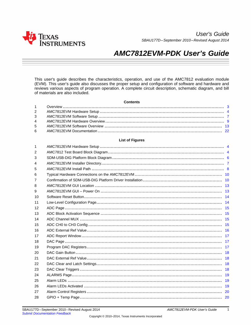
User's GuideSBAU177D–September 2010–Revised August 2014
AMC7812EVM-PDK User’s Guide
This user's guide describes the characteristics, operation, and use of the AMC7812 evaluation module(EVM). This user’s guide also discusses the proper setup and configuration of software and hardware andreviews various aspects of program operation. A complete circuit description, schematic diagram, and billof materials are also included.
Contents1 Overview ...................................................................................................................... 32 AMC7812EVM Hardware Setup ........................................................................................... 43 AMC7812EVM Software Setup ............................................................................................ 74 AMC7812EVM Hardware Overview ....................................................................................... 95 AMC7812EVM Software Overview ...................................................................................... 136 AMC7812EVM Documentation ........................................................................................... 22
List of Figures
1 AMC7812EVM Hardware Setup ........................................................................................... 42 AMC7812 Test Board Block Diagram..................................................................................... 43 SDM-USB-DIG Platform Block Diagram .................................................................................. 64 AMC7812EVM Installer Directory.......................................................................................... 75 AMC7812EVM Install Path ................................................................................................. 86 Typical Hardware Connections on the AMC7812EVM ................................................................ 107 Confirmation of SDM-USB-DIG Platform Driver Installation .......................................................... 108 AMC7812EVM GUI Location ............................................................................................. 139 AMC7812EVM GUI – Power On ......................................................................................... 1310 Software Reset Button..................................................................................................... 1411 Low-Level Configuration Page............................................................................................ 1412 ADC Page ................................................................................................................... 1513 ADC Block Activation Sequence ......................................................................................... 1514 ADC Channel MUX ........................................................................................................ 1515 ADC CH0 to CH3 Config .................................................................................................. 1516 ADC External Ref Value................................................................................................... 1617 ADC Report Window....................................................................................................... 1718 DAC Page ................................................................................................................... 1719 Program DAC Registers................................................................................................... 1720 DAC Gain Button ........................................................................................................... 1821 DAC External Ref Value................................................................................................... 1822 DAC Clear and Latch Settings............................................................................................ 1823 DAC Clear Triggers ........................................................................................................ 1824 ALARMS Page.............................................................................................................. 1925 Alarm LEDs ................................................................................................................. 1926 Alarm LEDs Activated ..................................................................................................... 1927 Alarm Control Registers ................................................................................................... 2028 GPIO + Temp Page ........................................................................................................ 20
1SBAU177D–September 2010–Revised August 2014 AMC7812EVM-PDK User’s GuideSubmit Documentation Feedback
Copyright © 2010–2014, Texas Instruments Incorporated
www.ti.com
29 Temperature Read ......................................................................................................... 2030 Threshold Limit Configuration ............................................................................................ 2131 Temperature Conversion Rate ........................................................................................... 2132 GPIO Page .................................................................................................................. 2133 GPIO Write/Read........................................................................................................... 2134 AMC7812EVM Schematic (1 of 3) ....................................................................................... 2235 AMC7812EVM Schematic (2 of 3) ....................................................................................... 2336 AMC7812EVM Schematic (3 of 3) ....................................................................................... 2437 AMC7812EVM PCB Components Layout............................................................................... 25
List of Tables
1 Contents of AMC7812EVM Kit ............................................................................................. 32 Related Documentation ..................................................................................................... 33 J1 Signal Definition .......................................................................................................... 54 Default Jumper Settings .................................................................................................... 95 AMC7812EVM Jumper and Shunt Resistor Settings.................................................................. 116 AMC7812EVM ADC Signal Connections ............................................................................... 117 AMC7812EVM DAC Signal Connections ............................................................................... 128 AMC7812EVM GPIO Signal Definition .................................................................................. 129 Conversion Rates .......................................................................................................... 1610 Bill of Materials ............................................................................................................. 26
2 AMC7812EVM-PDK User’s Guide SBAU177D–September 2010–Revised August 2014Submit Documentation Feedback
Copyright © 2010–2014, Texas Instruments Incorporated
www.ti.com Overview
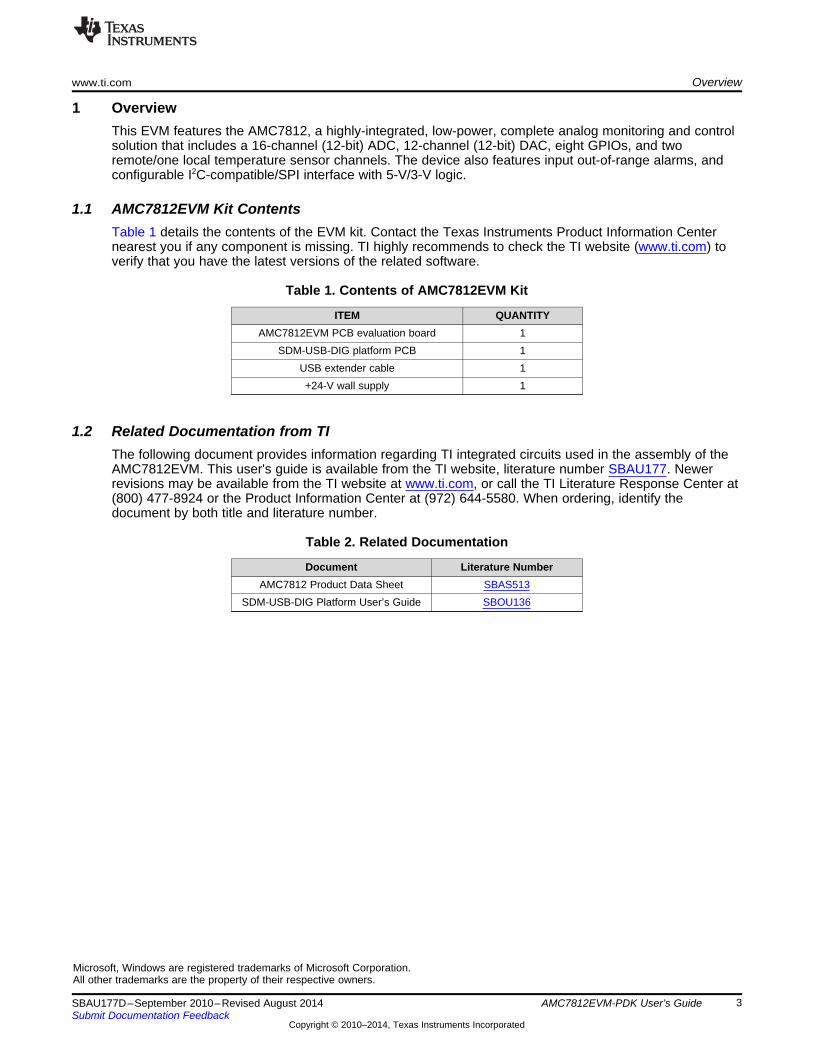
1 OverviewThis EVM features the AMC7812, a highly-integrated, low-power, complete analog monitoring and controlsolution that includes a 16-channel (12-bit) ADC, 12-channel (12-bit) DAC, eight GPIOs, and tworemote/one local temperature sensor channels. The device also features input out-of-range alarms, andconfigurable I2C-compatible/SPI interface with 5-V/3-V logic.
1.1 AMC7812EVM Kit ContentsTable 1 details the contents of the EVM kit. Contact the Texas Instruments Product Information Centernearest you if any component is missing. TI highly recommends to check the TI website (www.ti.com) toverify that you have the latest versions of the related software.
Table 1. Contents of AMC7812EVM Kit
ITEM QUANTITYAMC7812EVM PCB evaluation board 1
SDM-USB-DIG platform PCB 1USB extender cable 1+24-V wall supply 1
1.2 Related Documentation from TIThe following document provides information regarding TI integrated circuits used in the assembly of theAMC7812EVM. This user's guide is available from the TI website, literature number SBAU177. Newerrevisions may be available from the TI website at www.ti.com, or call the TI Literature Response Center at(800) 477-8924 or the Product Information Center at (972) 644-5580. When ordering, identify thedocument by both title and literature number.
Table 2. Related Documentation
Document Literature NumberAMC7812 Product Data Sheet SBAS513
SDM-USB-DIG Platform User’s Guide SBOU136
Microsoft, Windows are registered trademarks of Microsoft Corporation.All other trademarks are the property of their respective owners.
3SBAU177D–September 2010–Revised August 2014 AMC7812EVM-PDK User’s GuideSubmit Documentation Feedback
Copyright © 2010–2014, Texas Instruments Incorporated
Default:LDO Regulated
Power
20-PinConn. To
SDM-USB-DIG
16-CH ADC Input
8 GPIOConnection
12-CH DAC Vout
Optional:External Power
(Terminal Blocks)
AMC7812SPI
Power
AMC7812EVM
USB Bus from
Computer
+24-V Wall Adapter or
Optional External Power
20-PinConnectorSDM-USB-
DIG
J1 connection or terminal blocks
Personal Computer
(PC)
AMC7812EVM Hardware Setup www.ti.com
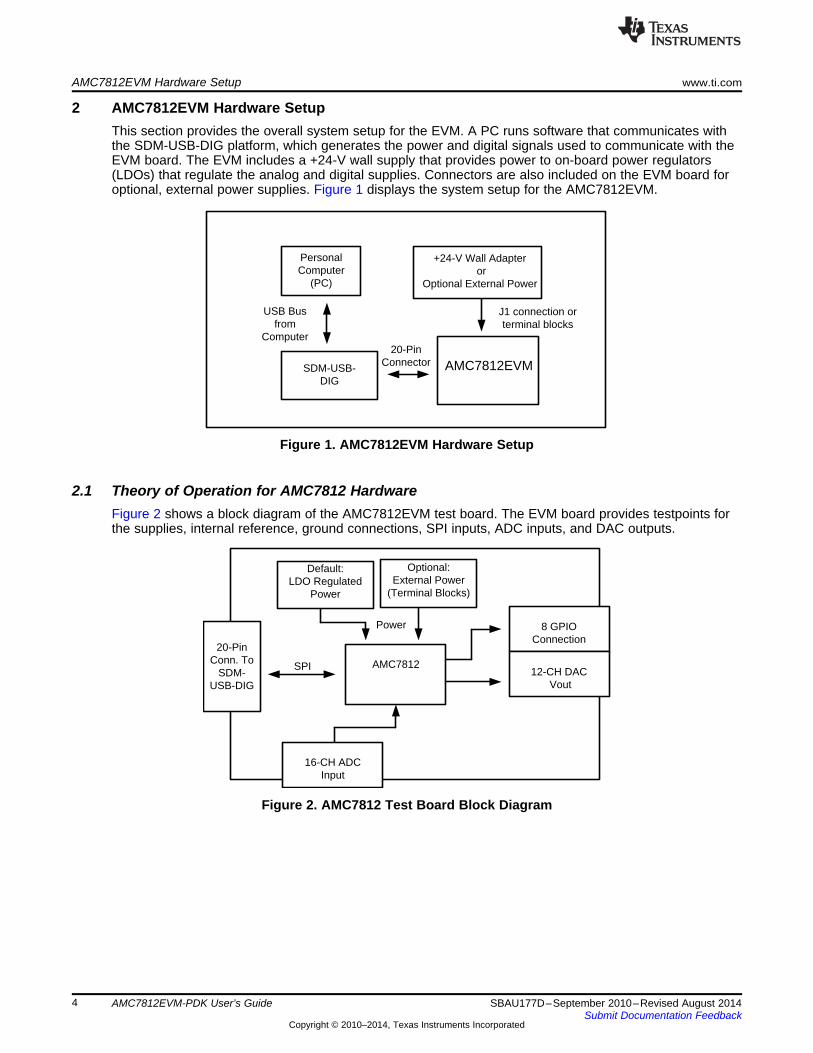
2 AMC7812EVM Hardware SetupThis section provides the overall system setup for the EVM. A PC runs software that communicates withthe SDM-USB-DIG platform, which generates the power and digital signals used to communicate with theEVM board. The EVM includes a +24-V wall supply that provides power to on-board power regulators(LDOs) that regulate the analog and digital supplies. Connectors are also included on the EVM board foroptional, external power supplies. Figure 1 displays the system setup for the AMC7812EVM.
Figure 1. AMC7812EVM Hardware Setup
2.1 Theory of Operation for AMC7812 HardwareFigure 2 shows a block diagram of the AMC7812EVM test board. The EVM board provides testpoints forthe supplies, internal reference, ground connections, SPI inputs, ADC inputs, and DAC outputs.
Figure 2. AMC7812 Test Board Block Diagram
4 AMC7812EVM-PDK User’s Guide SBAU177D–September 2010–Revised August 2014Submit Documentation Feedback
Copyright © 2010–2014, Texas Instruments Incorporated
www.ti.com AMC7812EVM Hardware Setup
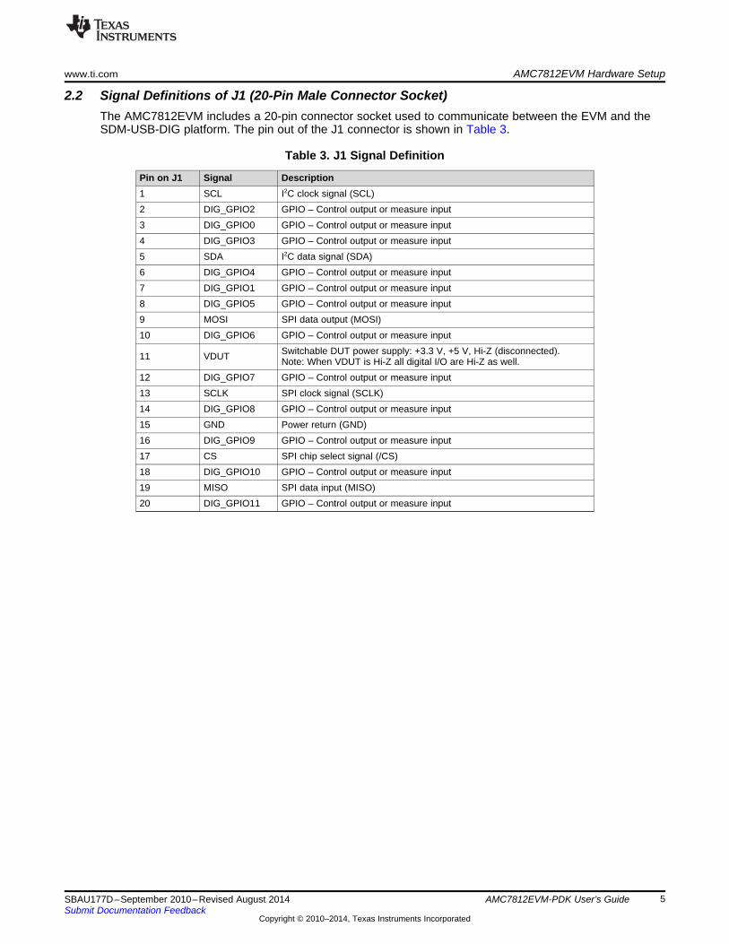
2.2 Signal Definitions of J1 (20-Pin Male Connector Socket)The AMC7812EVM includes a 20-pin connector socket used to communicate between the EVM and theSDM-USB-DIG platform. The pin out of the J1 connector is shown in Table 3.
Table 3. J1 Signal Definition
Pin on J1 Signal Description1 SCL I2C clock signal (SCL)2 DIG_GPIO2 GPIO – Control output or measure input3 DIG_GPIO0 GPIO – Control output or measure input4 DIG_GPIO3 GPIO – Control output or measure input5 SDA I2C data signal (SDA)6 DIG_GPIO4 GPIO – Control output or measure input7 DIG_GPIO1 GPIO – Control output or measure input8 DIG_GPIO5 GPIO – Control output or measure input9 MOSI SPI data output (MOSI)10 DIG_GPIO6 GPIO – Control output or measure input
Switchable DUT power supply: +3.3 V, +5 V, Hi-Z (disconnected).11 VDUT Note: When VDUT is Hi-Z all digital I/O are Hi-Z as well.12 DIG_GPIO7 GPIO – Control output or measure input13 SCLK SPI clock signal (SCLK)14 DIG_GPIO8 GPIO – Control output or measure input15 GND Power return (GND)16 DIG_GPIO9 GPIO – Control output or measure input17 CS SPI chip select signal (/CS)18 DIG_GPIO10 GPIO – Control output or measure input19 MISO SPI data input (MISO)20 DIG_GPIO11 GPIO – Control output or measure input
5SBAU177D–September 2010–Revised August 2014 AMC7812EVM-PDK User’s GuideSubmit Documentation Feedback
Copyright © 2010–2014, Texas Instruments Incorporated
MSP430F5528 Microcontroller
USB Bus from
Computer
3.3-V Regulator
+3.3 V
USB +5.0 V
Level Translators
Power Switching
Vdut(Hi-Z, 3.3 V or 5 V) Switched Power
I2CSPI
GPIO
Power on Reset
SDM-USB-DIG To
Test B
oard
To
Co
mp
uter an
d P
ow
er Su
pp
lies
+3.3 VUSB +5.0 V
AMC7812EVM Hardware Setup www.ti.com
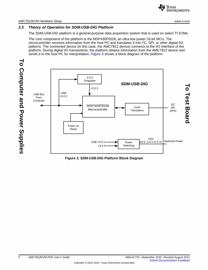
2.3 Theory of Operation for SDM-USB-DIG PlatformThe SDM-USB-DIG platform is a general-purpose data acquisition system that is used on select TI EVMs.
The core component of the platform is the MSP430F5528, an ultra-low power 16-bit MCU. Themicrocontroller receives information from the host PC and translates it into I2C, SPI, or other digital I/Opatterns. The connected device (in this case, the AMC7812 device) connects to the I/O interface of theplatform. During digital I/O transactions, the platform obtains information from the AMC7812 device andsends it to the host PC for interpretation. Figure 3 shows a block diagram of the platform.
Figure 3. SDM-USB-DIG Platform Block Diagram
6 AMC7812EVM-PDK User’s Guide SBAU177D–September 2010–Revised August 2014Submit Documentation Feedback
Copyright © 2010–2014, Texas Instruments Incorporated
www.ti.com AMC7812EVM Software Setup
3 AMC7812EVM Software SetupThis section provides the procedure for EVM software installation.
3.1 Operating Systems for AMC7812EVM SoftwareThe EVM software was tested on the Microsoft® Windows® XP and Windows 7 operating systems with theUnited States and European regional settings. The software should also be compatible with otherWindows operating systems.
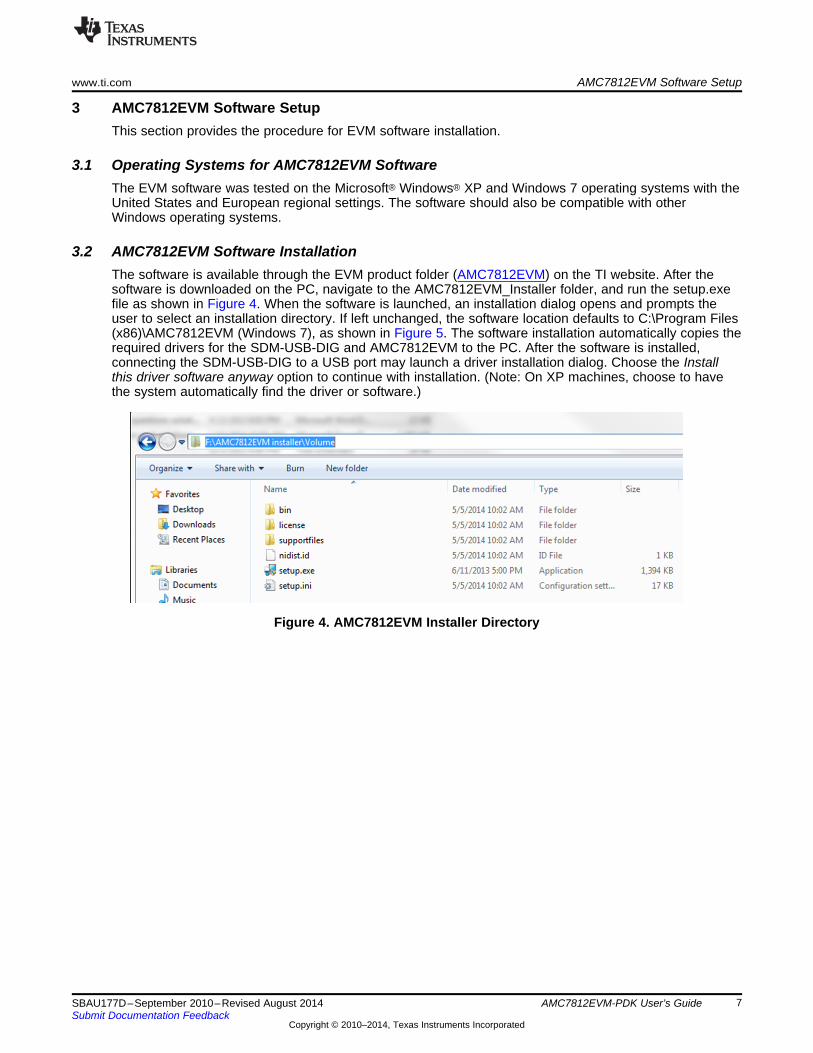
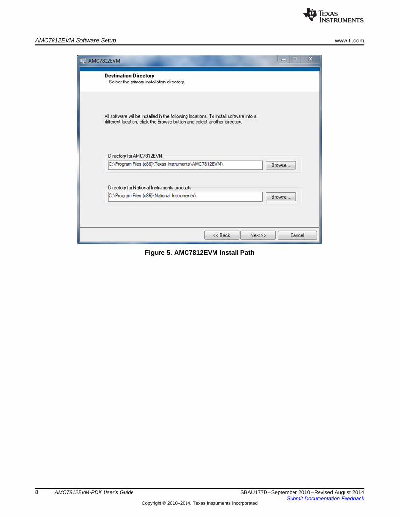
3.2 AMC7812EVM Software InstallationThe software is available through the EVM product folder (AMC7812EVM) on the TI website. After thesoftware is downloaded on the PC, navigate to the AMC7812EVM_Installer folder, and run the setup.exefile as shown in Figure 4. When the software is launched, an installation dialog opens and prompts theuser to select an installation directory. If left unchanged, the software location defaults to C:\Program Files(x86)\AMC7812EVM (Windows 7), as shown in Figure 5. The software installation automatically copies therequired drivers for the SDM-USB-DIG and AMC7812EVM to the PC. After the software is installed,connecting the SDM-USB-DIG to a USB port may launch a driver installation dialog. Choose the Installthis driver software anyway option to continue with installation. (Note: On XP machines, choose to havethe system automatically find the driver or software.)
Figure 4. AMC7812EVM Installer Directory
7SBAU177D–September 2010–Revised August 2014 AMC7812EVM-PDK User’s GuideSubmit Documentation Feedback
Copyright © 2010–2014, Texas Instruments Incorporated
AMC7812EVM Software Setup www.ti.com
Figure 5. AMC7812EVM Install Path
8 AMC7812EVM-PDK User’s Guide SBAU177D–September 2010–Revised August 2014Submit Documentation Feedback
Copyright © 2010–2014, Texas Instruments Incorporated
www.ti.com AMC7812EVM Hardware Overview
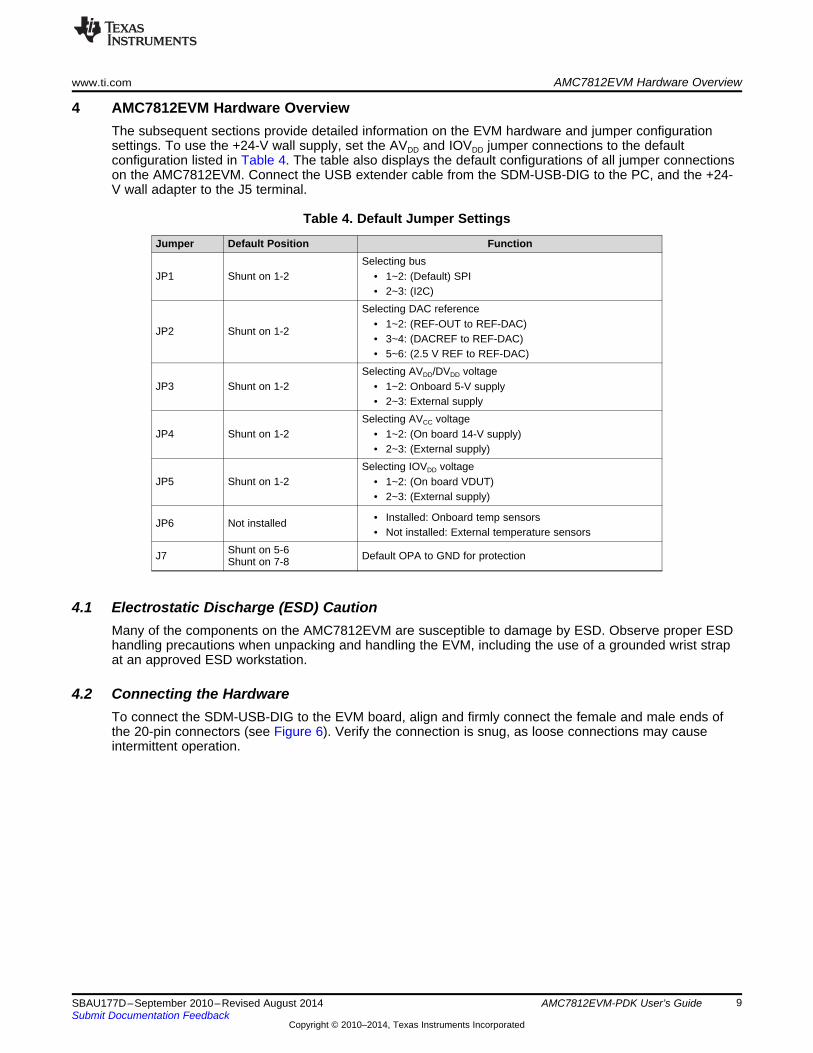
4 AMC7812EVM Hardware OverviewThe subsequent sections provide detailed information on the EVM hardware and jumper configurationsettings. To use the +24-V wall supply, set the AVDD and IOVDD jumper connections to the defaultconfiguration listed in Table 4. The table also displays the default configurations of all jumper connectionson the AMC7812EVM. Connect the USB extender cable from the SDM-USB-DIG to the PC, and the +24-V wall adapter to the J5 terminal.
Table 4. Default Jumper Settings
Jumper Default Position FunctionSelecting bus
JP1 Shunt on 1-2 • 1~2: (Default) SPI• 2~3: (I2C)
Selecting DAC reference• 1~2: (REF-OUT to REF-DAC)
JP2 Shunt on 1-2• 3~4: (DACREF to REF-DAC)• 5~6: (2.5 V REF to REF-DAC)
Selecting AVDD/DVDD voltageJP3 Shunt on 1-2 • 1~2: Onboard 5-V supply
• 2~3: External supplySelecting AVCC voltage
JP4 Shunt on 1-2 • 1~2: (On board 14-V supply)• 2~3: (External supply)
Selecting IOVDD voltageJP5 Shunt on 1-2 • 1~2: (On board VDUT)
• 2~3: (External supply)
• Installed: Onboard temp sensorsJP6 Not installed• Not installed: External temperature sensors
Shunt on 5-6J7 Default OPA to GND for protectionShunt on 7-8
4.1 Electrostatic Discharge (ESD) CautionMany of the components on the AMC7812EVM are susceptible to damage by ESD. Observe proper ESDhandling precautions when unpacking and handling the EVM, including the use of a grounded wrist strapat an approved ESD workstation.
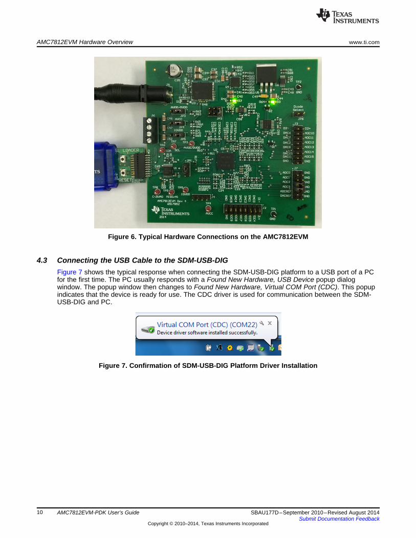
4.2 Connecting the HardwareTo connect the SDM-USB-DIG to the EVM board, align and firmly connect the female and male ends ofthe 20-pin connectors (see Figure 6). Verify the connection is snug, as loose connections may causeintermittent operation.
9SBAU177D–September 2010–Revised August 2014 AMC7812EVM-PDK User’s GuideSubmit Documentation Feedback
Copyright © 2010–2014, Texas Instruments Incorporated
AMC7812EVM Hardware Overview www.ti.com
Figure 6. Typical Hardware Connections on the AMC7812EVM
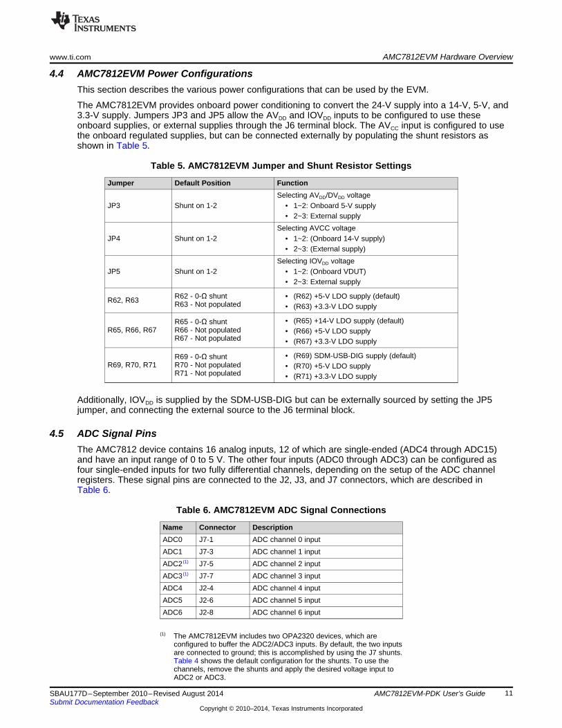
4.3 Connecting the USB Cable to the SDM-USB-DIGFigure 7 shows the typical response when connecting the SDM-USB-DIG platform to a USB port of a PCfor the first time. The PC usually responds with a Found New Hardware, USB Device popup dialogwindow. The popup window then changes to Found New Hardware, Virtual COM Port (CDC). This popupindicates that the device is ready for use. The CDC driver is used for communication between the SDM-USB-DIG and PC.
Figure 7. Confirmation of SDM-USB-DIG Platform Driver Installation
10 AMC7812EVM-PDK User’s Guide SBAU177D–September 2010–Revised August 2014Submit Documentation Feedback
Copyright © 2010–2014, Texas Instruments Incorporated
www.ti.com AMC7812EVM Hardware Overview
4.4 AMC7812EVM Power ConfigurationsThis section describes the various power configurations that can be used by the EVM.
The AMC7812EVM provides onboard power conditioning to convert the 24-V supply into a 14-V, 5-V, and3.3-V supply. Jumpers JP3 and JP5 allow the AVDD and IOVDD inputs to be configured to use theseonboard supplies, or external supplies through the J6 terminal block. The AVCC input is configured to usethe onboard regulated supplies, but can be connected externally by populating the shunt resistors asshown in Table 5.
Table 5. AMC7812EVM Jumper and Shunt Resistor Settings
Jumper Default Position FunctionSelecting AVDD/DVDD voltage
JP3 Shunt on 1-2 • 1~2: Onboard 5-V supply• 2~3: External supply
Selecting AVCC voltageJP4 Shunt on 1-2 • 1~2: (Onboard 14-V supply)
• 2~3: (External supply)Selecting IOVDD voltage
JP5 Shunt on 1-2 • 1~2: (Onboard VDUT)• 2~3: External supply
R62 - 0-Ω shunt • (R62) +5-V LDO supply (default)R62, R63 R63 - Not populated • (R63) +3.3-V LDO supply
• (R65) +14-V LDO supply (default)R65 - 0-Ω shuntR65, R66, R67 R66 - Not populated • (R66) +5-V LDO supply
R67 - Not populated • (R67) +3.3-V LDO supply
• (R69) SDM-USB-DIG supply (default)R69 - 0-Ω shuntR69, R70, R71 R70 - Not populated • (R70) +5-V LDO supply
R71 - Not populated • (R71) +3.3-V LDO supply
Additionally, IOVDD is supplied by the SDM-USB-DIG but can be externally sourced by setting the JP5jumper, and connecting the external source to the J6 terminal block.
4.5 ADC Signal PinsThe AMC7812 device contains 16 analog inputs, 12 of which are single-ended (ADC4 through ADC15)and have an input range of 0 to 5 V. The other four inputs (ADC0 through ADC3) can be configured asfour single-ended inputs for two fully differential channels, depending on the setup of the ADC channelregisters. These signal pins are connected to the J2, J3, and J7 connectors, which are described inTable 6.
Table 6. AMC7812EVM ADC Signal Connections
Name Connector DescriptionADC0 J7-1 ADC channel 0 inputADC1 J7-3 ADC channel 1 inputADC2 (1) J7-5 ADC channel 2 inputADC3 (1) J7-7 ADC channel 3 inputADC4 J2-4 ADC channel 4 inputADC5 J2-6 ADC channel 5 inputADC6 J2-8 ADC channel 6 input
(1) The AMC7812EVM includes two OPA2320 devices, which areconfigured to buffer the ADC2/ADC3 inputs. By default, the two inputsare connected to ground; this is accomplished by using the J7 shunts.Table 4 shows the default configuration for the shunts. To use thechannels, remove the shunts and apply the desired voltage input toADC2 or ADC3.
11SBAU177D–September 2010–Revised August 2014 AMC7812EVM-PDK User’s GuideSubmit Documentation Feedback
Copyright © 2010–2014, Texas Instruments Incorporated
AMC7812EVM Hardware Overview www.ti.com
Table 6. AMC7812EVM ADC SignalConnections (continued)
Name Connector DescriptionADC7 J2-10 ADC channel 7 inputADC8 J2-12 ADC channel 8 inputADC9 J2-14 ADC channel 9 inputADC10 J3-4 ADC channel 10 inputADC11 J3-6 ADC channel 11 inputADC12 J3-8 ADC channel 12 inputADC13 J3-10 ADC channel 13 inputADC14 J3-12 ADC channel 14 inputADC15 J3-14 ADC channel 15 input
4.6 DAC Signal PinsThe 12 DAC voltage outputs of the AMC7812 device are accessible through the J2 and J3 connectors, asshown in Table 4. The DAC voltage ranges are configurable through software to either 5 or 12.5 V.
Table 7. AMC7812EVM DAC Signal Connections
Name Connector DescriptionDACC0 J2-3 DAC-C0 outputDACC1 J2-5 DAC-C1 outputDACD2 J2-7 DAC-D2 outputDACD3 J2-9 DAC-D3 outputDACD4 J2-11 DAC-D4 outputDACD5 J2-13 DAC-D5 outputDACB6 J3-3 DAC-B6 outputDACB7 J3-5 DAC-B7 outputDACA8 J3-7 DAC-A8 outputDACA9 J3-9 DAC-A9 outputDACA10 J3-11 DAC-A10 outputDACA11 J3-13 DAC-A11 output
4.7 GPIO Signal PinsThe four GPIO signals on the EVM can be measured on the J4 header. Table 8 provides a signaldescription of the J4 header.
Table 8. AMC7812EVM GPIO Signal Definition (1)
Name Connector DescriptionGPIO0 J4-4 General-purpose I/O (GPIO0)GPIO1 J4-3 General-purpose I/O (GPIO1)GPIO2 J4-2 General-purpose I/O (GPIO2)GPIO3 J4-1 General-purpose I/O (GPIO3)
(1) The remote sensor channels, D1+/D1– and D2+/D2–, can be configured as GPIO, if remotetemperature sensors are not needed. Use a shunt to connect JP6 to remove the connection to theonboard remote temperature sensors.
12 AMC7812EVM-PDK User’s Guide SBAU177D–September 2010–Revised August 2014Submit Documentation Feedback
Copyright © 2010–2014, Texas Instruments Incorporated
www.ti.com AMC7812EVM Software Overview
5 AMC7812EVM Software OverviewThis section discusses how to use the AMC7812EVM software.
5.1 Starting the AMC7812EVM SoftwareAfter the hardware connections are established and jumper settings configured, launch the softwarelocated in the AMC7812EVM folder of the Start All Programs menu, and select the AMC7812EVM icon.
Figure 8. AMC7812EVM GUI Location
If the SDM-USB-DIG is properly connected to the AMC7812EVM, the GUI should automatically power onthe system and display CONNECTED: Power On in the upper right area of the GUI (see Figure 9).
Figure 9. AMC7812EVM GUI – Power On
If the SDM-USB-DIG has a faulty connection, or is not connected at all, the GUI launches in simulationmode. In simulation mode, NOT CONNECTED: Simulating is displayed in the top-right area of the GUI. Ifthis text appears while the SDM-USB-DIG device is connected, then unplug the SDM-USB-DIG and closethe GUI. Reconnect the SDM-USB-DIG, and ensure that the connectors are correctly aligned. After doingthose steps, verify the USB extender cable is properly connected to both the SDM-USB-DIG and PC, andrelaunch the GUI. This connection issue can also occur if the CDC driver is installed incorrectly. TheAMC7812EVM software may need to be reinstalled.
5.2 AMC7812EVM Software FeaturesThe following subsections describe the functionality of each page of the AMC7812EVM GUI.
5.2.1 Software ResetThe AMC7812 Software Reset button, shown in Figure 10, resets the AMC7812 device and resets allregisters to their default settings.
13SBAU177D–September 2010–Revised August 2014 AMC7812EVM-PDK User’s GuideSubmit Documentation Feedback
Copyright © 2010–2014, Texas Instruments Incorporated
AMC7812EVM Software Overview www.ti.com
Figure 10. Software Reset Button
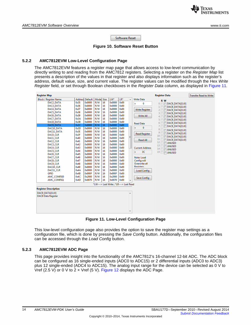
5.2.2 AMC7812EVM Low-Level Configuration PageThe AMC7812EVM features a register map page that allows access to low-level communication bydirectly writing to and reading from the AMC7812 registers. Selecting a register on the Register Map listpresents a description of the values in that register and also displays information such as the register’saddress, default value, size, and current value. The register values can be modified through the Hex WriteRegister field, or set through Boolean checkboxes in the Register Data column, as displayed in Figure 11.
Figure 11. Low-Level Configuration Page
This low-level configuration page also provides the option to save the register map settings as aconfiguration file, which is done by pressing the Save Config button. Additionally, the configuration filescan be accessed through the Load Config button.
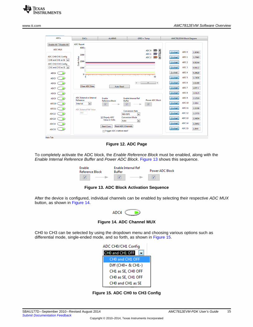
5.2.3 AMC7812EVM ADC PageThis page provides insight into the functionality of the AMC7812’s 16-channel 12-bit ADC. The ADC blockcan be configured as 16 single-ended inputs (ADC0 to ADC15) or 2 differential inputs (ADC0 to ADC3)plus 12 single-ended (ADC4 to ADC15). The analog input range for the device can be selected as 0 V toVref (2.5 V) or 0 V to 2 × Vref (5 V). Figure 12 displays the ADC Page.
14 AMC7812EVM-PDK User’s Guide SBAU177D–September 2010–Revised August 2014Submit Documentation Feedback
Copyright © 2010–2014, Texas Instruments Incorporated
www.ti.com AMC7812EVM Software Overview
Figure 12. ADC Page
To completely activate the ADC block, the Enable Reference Block must be enabled, along with theEnable Internal Reference Buffer and Power ADC Block. Figure 13 shows this sequence.
Figure 13. ADC Block Activation Sequence
After the device is configured, individual channels can be enabled by selecting their respective ADC MUXbutton, as shown in Figure 14.
Figure 14. ADC Channel MUX
CH0 to CH3 can be selected by using the dropdown menu and choosing various options such asdifferential mode, single-ended mode, and so forth, as shown in Figure 15.
Figure 15. ADC CH0 to CH3 Config
15SBAU177D–September 2010–Revised August 2014 AMC7812EVM-PDK User’s GuideSubmit Documentation Feedback
Copyright © 2010–2014, Texas Instruments Incorporated
AMC7812EVM Software Overview www.ti.com
The input range can be adjusted by clicking the button next to each ADC channel on the right-hand side ofthe page. Conversions can be triggered by pressing the Start Conv button or can be automaticallytriggered before every read by enabling the Auto-Trigger check box. The ADC data registers, displayed onthe right side of the GUI, are updated with the converted results when the Read ADC button is pressed.
NOTE: The AMC7812EVM includes two OPA2320 devices, which are configured to buffer theADC2/ADC3 inputs. By default, the two inputs are connected to ground, this is accomplishedby using the J7 shunts. The default configuration for the shunts are located in Table 4. Touse the channels, remove the shunts and apply the desired voltage input to ADC2 or ADC3.
Most of the controls listed within the ADC image are used to setup the ADC configuration register. Theseinclude the conversion rate and conversion mode parameters, which are selectable through theirrespective dropdown list. The selectable conversion rates are listed in Table 9.
Table 9. Conversion Rates
Throughput (ADC0–ADC11)Conversion Rate (Single-Channel Auto Mode)00 500 kSPS01 250 kSPS10 125 kSPS11 62.5 kSPS
The conversion mode can be either Auto or Direct mode. In Direct Mode, the analog inputs, specified inthe ADC channel registers, are converted sequentially one time. In Auto Mode, the analog inputs areconverted sequentially and repeatedly. After a conversion is completed, the ADC multiplexer returns to thefirst channel and repeats the process.
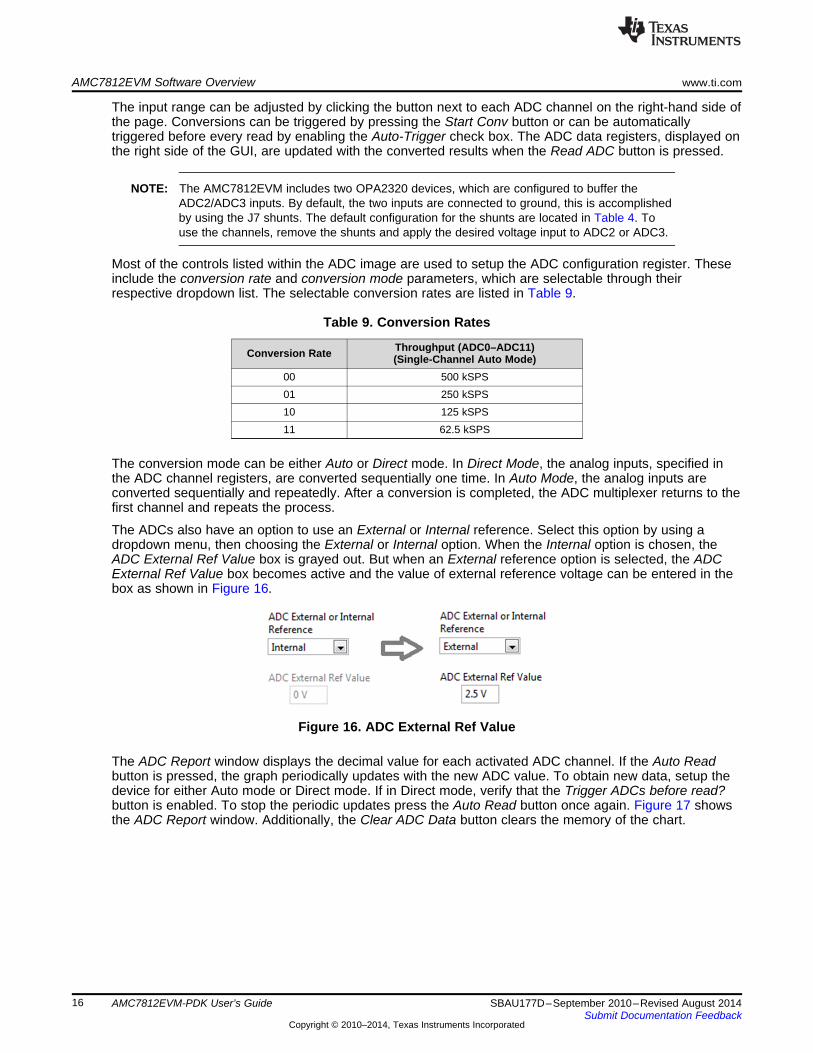
The ADCs also have an option to use an External or Internal reference. Select this option by using adropdown menu, then choosing the External or Internal option. When the Internal option is chosen, theADC External Ref Value box is grayed out. But when an External reference option is selected, the ADCExternal Ref Value box becomes active and the value of external reference voltage can be entered in thebox as shown in Figure 16.
Figure 16. ADC External Ref Value
The ADC Report window displays the decimal value for each activated ADC channel. If the Auto Readbutton is pressed, the graph periodically updates with the new ADC value. To obtain new data, setup thedevice for either Auto mode or Direct mode. If in Direct mode, verify that the Trigger ADCs before read?button is enabled. To stop the periodic updates press the Auto Read button once again. Figure 17 showsthe ADC Report window. Additionally, the Clear ADC Data button clears the memory of the chart.
16 AMC7812EVM-PDK User’s Guide SBAU177D–September 2010–Revised August 2014Submit Documentation Feedback
Copyright © 2010–2014, Texas Instruments Incorporated
www.ti.com AMC7812EVM Software Overview
Figure 17. ADC Report Window
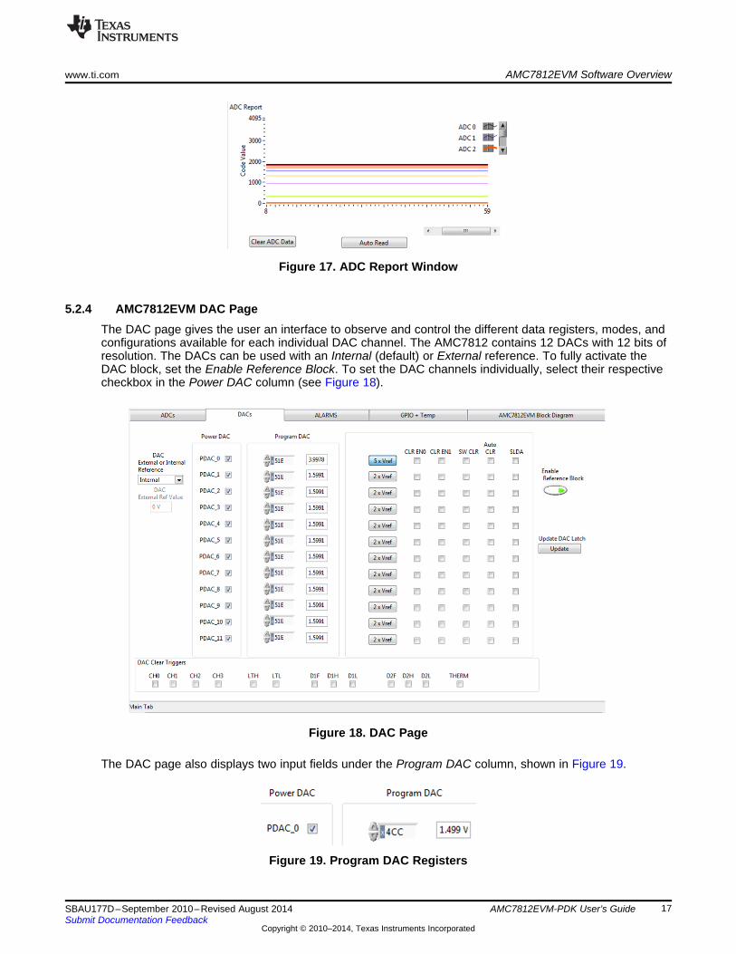
5.2.4 AMC7812EVM DAC PageThe DAC page gives the user an interface to observe and control the different data registers, modes, andconfigurations available for each individual DAC channel. The AMC7812 contains 12 DACs with 12 bits ofresolution. The DACs can be used with an Internal (default) or External reference. To fully activate theDAC block, set the Enable Reference Block. To set the DAC channels individually, select their respectivecheckbox in the Power DAC column (see Figure 18).
Figure 18. DAC Page
The DAC page also displays two input fields under the Program DAC column, shown in Figure 19.
Figure 19. Program DAC Registers
17SBAU177D–September 2010–Revised August 2014 AMC7812EVM-PDK User’s GuideSubmit Documentation Feedback
Copyright © 2010–2014, Texas Instruments Incorporated
AMC7812EVM Software Overview www.ti.com
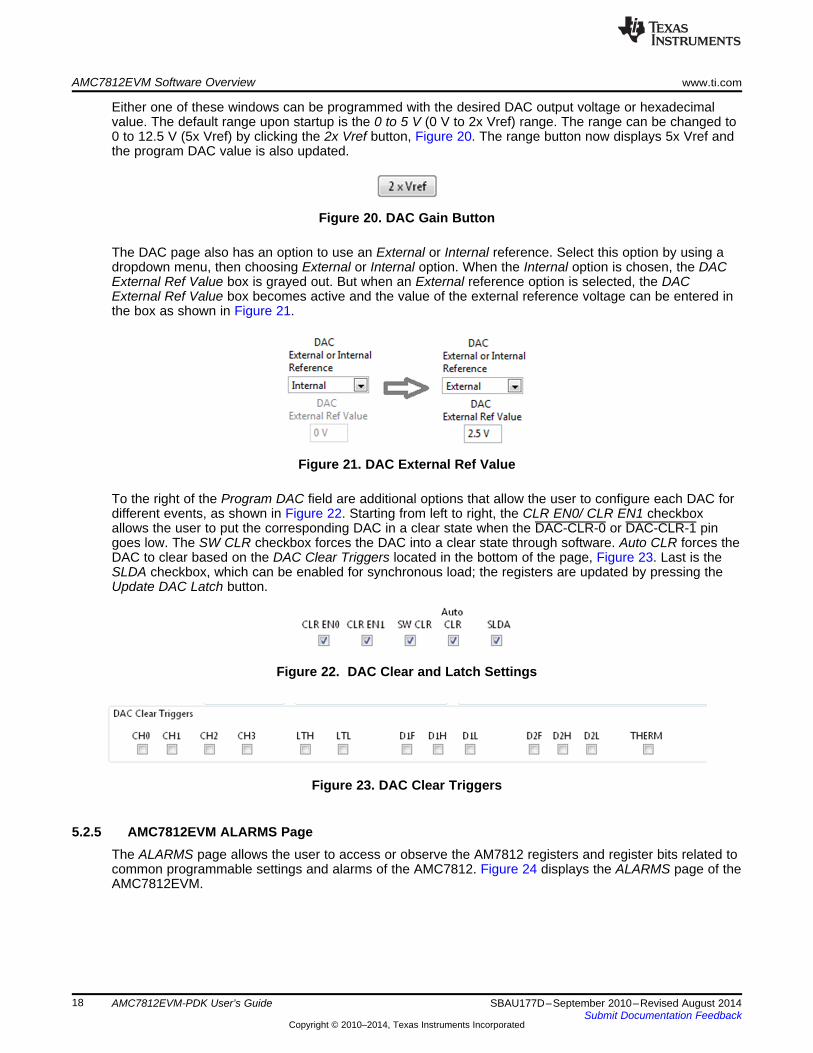
Either one of these windows can be programmed with the desired DAC output voltage or hexadecimalvalue. The default range upon startup is the 0 to 5 V (0 V to 2x Vref) range. The range can be changed to0 to 12.5 V (5x Vref) by clicking the 2x Vref button, Figure 20. The range button now displays 5x Vref andthe program DAC value is also updated.
Figure 20. DAC Gain Button
The DAC page also has an option to use an External or Internal reference. Select this option by using adropdown menu, then choosing External or Internal option. When the Internal option is chosen, the DACExternal Ref Value box is grayed out. But when an External reference option is selected, the DACExternal Ref Value box becomes active and the value of the external reference voltage can be entered inthe box as shown in Figure 21.
Figure 21. DAC External Ref Value
To the right of the Program DAC field are additional options that allow the user to configure each DAC fordifferent events, as shown in Figure 22. Starting from left to right, the CLR EN0/ CLR EN1 checkboxallows the user to put the corresponding DAC in a clear state when the DAC-CLR-0 or DAC-CLR-1 pingoes low. The SW CLR checkbox forces the DAC into a clear state through software. Auto CLR forces theDAC to clear based on the DAC Clear Triggers located in the bottom of the page, Figure 23. Last is theSLDA checkbox, which can be enabled for synchronous load; the registers are updated by pressing theUpdate DAC Latch button.
Figure 22. DAC Clear and Latch Settings
Figure 23. DAC Clear Triggers
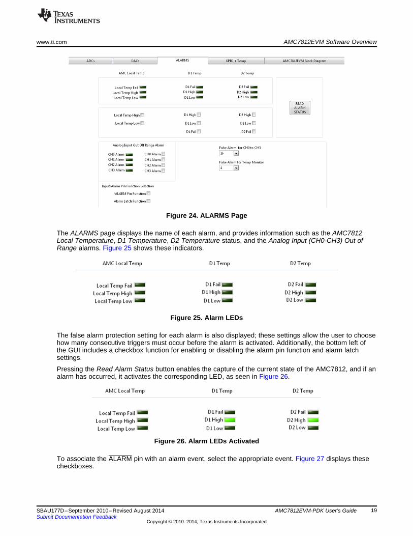
5.2.5 AMC7812EVM ALARMS PageThe ALARMS page allows the user to access or observe the AM7812 registers and register bits related tocommon programmable settings and alarms of the AMC7812. Figure 24 displays the ALARMS page of theAMC7812EVM.
18 AMC7812EVM-PDK User’s Guide SBAU177D–September 2010–Revised August 2014Submit Documentation Feedback
Copyright © 2010–2014, Texas Instruments Incorporated
www.ti.com AMC7812EVM Software Overview
Figure 24. ALARMS Page
The ALARMS page displays the name of each alarm, and provides information such as the AMC7812Local Temperature, D1 Temperature, D2 Temperature status, and the Analog Input (CH0-CH3) Out ofRange alarms. Figure 25 shows these indicators.
Figure 25. Alarm LEDs
The false alarm protection setting for each alarm is also displayed; these settings allow the user to choosehow many consecutive triggers must occur before the alarm is activated. Additionally, the bottom left ofthe GUI includes a checkbox function for enabling or disabling the alarm pin function and alarm latchsettings.
Pressing the Read Alarm Status button enables the capture of the current state of the AMC7812, and if analarm has occurred, it activates the corresponding LED, as seen in Figure 26.
Figure 26. Alarm LEDs Activated
To associate the ALARM pin with an alarm event, select the appropriate event. Figure 27 displays thesecheckboxes.
19SBAU177D–September 2010–Revised August 2014 AMC7812EVM-PDK User’s GuideSubmit Documentation Feedback
Copyright © 2010–2014, Texas Instruments Incorporated
AMC7812EVM Software Overview www.ti.com
Figure 27. Alarm Control Registers
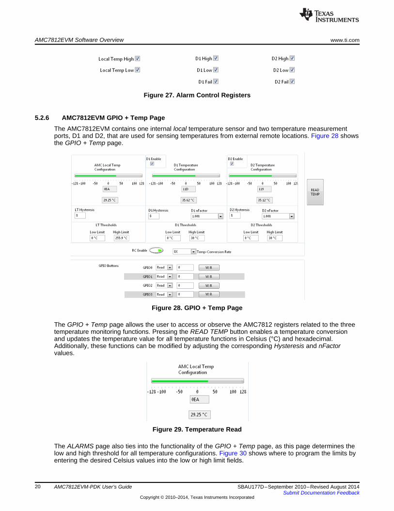
5.2.6 AMC7812EVM GPIO + Temp PageThe AMC7812EVM contains one internal local temperature sensor and two temperature measurementports, D1 and D2, that are used for sensing temperatures from external remote locations. Figure 28 showsthe GPIO + Temp page.
Figure 28. GPIO + Temp Page
The GPIO + Temp page allows the user to access or observe the AMC7812 registers related to the threetemperature monitoring functions. Pressing the READ TEMP button enables a temperature conversionand updates the temperature value for all temperature functions in Celsius (°C) and hexadecimal.Additionally, these functions can be modified by adjusting the corresponding Hysteresis and nFactorvalues.
Figure 29. Temperature Read
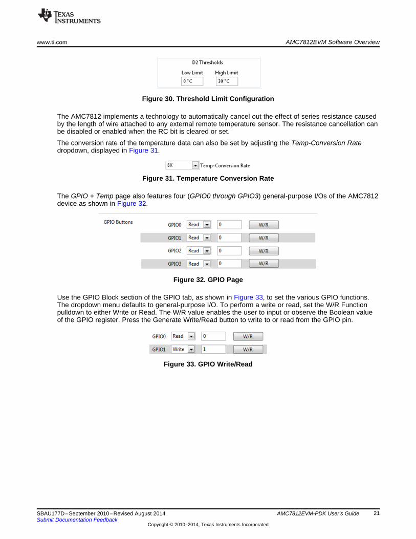
The ALARMS page also ties into the functionality of the GPIO + Temp page, as this page determines thelow and high threshold for all temperature configurations. Figure 30 shows where to program the limits byentering the desired Celsius values into the low or high limit fields.
20 AMC7812EVM-PDK User’s Guide SBAU177D–September 2010–Revised August 2014Submit Documentation Feedback
Copyright © 2010–2014, Texas Instruments Incorporated
www.ti.com AMC7812EVM Software Overview
Figure 30. Threshold Limit Configuration
The AMC7812 implements a technology to automatically cancel out the effect of series resistance causedby the length of wire attached to any external remote temperature sensor. The resistance cancellation canbe disabled or enabled when the RC bit is cleared or set.
The conversion rate of the temperature data can also be set by adjusting the Temp-Conversion Ratedropdown, displayed in Figure 31.
Figure 31. Temperature Conversion Rate
The GPIO + Temp page also features four (GPIO0 through GPIO3) general-purpose I/Os of the AMC7812device as shown in Figure 32.
Figure 32. GPIO Page
Use the GPIO Block section of the GPIO tab, as shown in Figure 33, to set the various GPIO functions.The dropdown menu defaults to general-purpose I/O. To perform a write or read, set the W/R Functionpulldown to either Write or Read. The W/R value enables the user to input or observe the Boolean valueof the GPIO register. Press the Generate Write/Read button to write to or read from the GPIO pin.
Figure 33. GPIO Write/Read
21SBAU177D–September 2010–Revised August 2014 AMC7812EVM-PDK User’s GuideSubmit Documentation Feedback
Copyright © 2010–2014, Texas Instruments Incorporated
SCL
DIG_GPIO0
SDA
DIG_GPIO1
MOSI
VDUT
DIG_GPIO6
DIG_GPIO2
DIG_GPIO3
DIG_GPIO4
DIG_GPIO5
SCLK
CS
MISO
0R42
TP1 TP2
AGND GND
MOSI/SDA
SCLK/SCL
CS/A0
MISO/A1
DIG_GPIO6
S1
1B12
1B23
1A4
2B15
2B26
2A7
3B210
GND8
3A9
3B111
4A12
4B213
4B114
OE15
VCC16
U1
TS5N412PW
0R310R32
0R330R34
0R350R36
0R370R38
0R390R40
0R410R43
0R200R21
0R220R23
1 2
3 4
5 6
7 8
9 10
11 12
13 14
15 16
J2
1 2
3 4
5 6
7 8
9 10
11 12
13 14
15 16
J3
AGND
0R250R26
0R120R13
0R140R15
0R160R19
DACREF
AMC D2+
AMC D1+AMC D1-
AMC D2-
DIG_GPIO3
DIG_GPIO4
DIG_GPIO2
DIG_GPIO5
DIG_GPIO1
AGND
GND
AVCC AGND
AVDD/DVDD
GND
IOVDD
ADC0
ADC1
ADC2
ADC3
AMC D1+
AMC D1-
AMC D2+
AMC D2-
AGND
4.7μF
C8
ADCREF
20.0kR27
20.0kR28
20.0kR29
20.0kR30
IOVDD
4
1
2
3
J4
AMC GPIO0AMC GPIO1AMC GPIO2AMC GPIO3
20.0kR11 20.0k
R10 20.0kR9 20.0k
R8 20.0kR7
IOVDD
IOVDD
0R40
R3
GNDGND
GND
IOVDD
0
R18
GND
SDA
SCL
DIG_GPIO6
SCLK/SCL
MOSI/SDA
CS/A0
MISO/A1
IOVDD
DACREF SEL
2.5V REF
DIG_GPIO0
1 2
3 4
5 6
JP2
SCLK
MOSI
CS
MISO
SPI / I2C MUXSDMini Dig Connector
1
3
56
4
2
7
910
8
12 11
14 13
16 15
18 17
20 19
J1
0.1μF
C2
0.1μF
C3
0.1μF
C5
0.1μF
C6
0.1μF
C4
0.1μF
C7
0.1μF
C1
GND
IOVDD
R5
NI R6
NI
R24
NI
C14
NI
C13
NI
C12
NI
C11
NI
C10
NI
C9
NI
C15
NI
C16
NI
C17
NI
C18
NI
C19
NI
C20
NI
C32
NI
C31
NI
C30
NI
C29
NI
C28
NI
C27
NI
C26
NI
C25
NI
C24
NI
C23
NI
C22
NI
C21
NI
SDMini Dig connector
RESET1
DAV2
CNVT3
SDI/SDA4
SCLK/SCL5
DG
ND
6
IOV
DD
7
DV
DD
8
CS/A09
SDO/A110
A211
SPI/I2C12
GPIO-013
GPIO-114
GPIO-215
GPIO-316
DAC-CLR-017
DAC5-OUT18
DAC4-OUT19
DAC3-OUT20
AG
ND
421
AG
ND
322
AV
CC
223
DAC2-OUT24
DAC1-OUT25
DAC0-OUT26
D2-/GPIO-627
D2+/GPIO-728
D1-/GPIO-429
D1+/GPIO-530
ADC-REF-IN/CMP31
ADC-GND32
CH033
CH134
CH235
CH336
CH437
CH538
CH639
CH740
CH841
CH942
CH1043
CH1144
CH1245
CH1346
CH1447
CH1548
AV
DD
149
AV
DD
250
DAC6-OUT51
DAC7-OUT52
DAC8-OUT53
AG
ND
154
AG
ND
255
AV
CC
156
REF-OUT57
REF-DAC58
DAC9-OUT59
DAC10-OUT60
DAC11-OUT61
ALARM62
DAC-CLR-163
DG
ND
264
PA
D
U2
AMC7812SRGC
AGND
20.0k
R1
20.0kR2
TP6 TP7 TP8 TP9
GND
IOVDD
0.01μF
C64
0.1μF
C65
GND
1
2
3
JP1
20.0kR17
AMC7812EVM Documentation www.ti.com
6 AMC7812EVM DocumentationThis section contains the schematic diagrams and complete bill of materials for the AMC7812EVM. Documentation information for the SDM-USB-DIG platform can be found in the SDM-USB-DIG Platform User’s Guide, SBOU136, available at the TI website at www.ti.com.
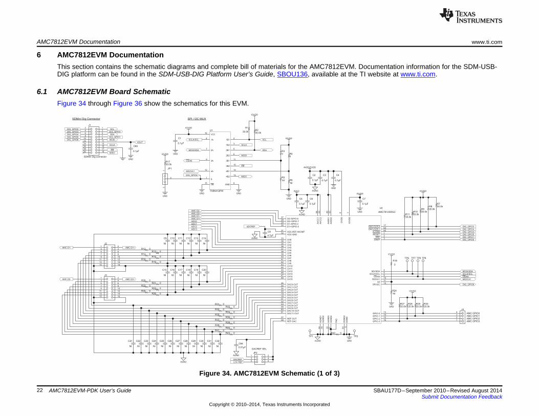
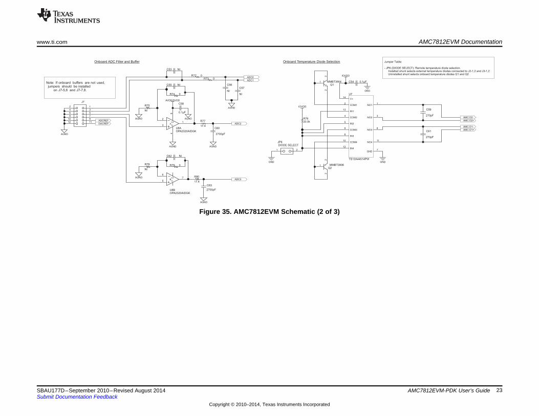
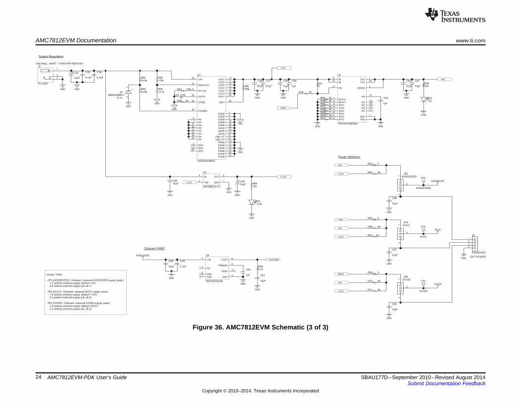
6.1 AMC7812EVM Board SchematicFigure 34 through Figure 36 show the schematics for this EVM.
Figure 34. AMC7812EVM Schematic (1 of 3)
22 AMC7812EVM-PDK User’s Guide SBAU177D–September 2010–Revised August 2014Submit Documentation Feedback
Copyright © 2010–2014, Texas Instruments Incorporated
NO11
COM12
NO23
COM24
IN25
IN36
GND7
NO38
COM39
COM410
NO411
IN412
IN113
V+14
U7
TS12A44514PW
2
3
1A
V+
V-
84
U8AOPA2320AIDGK
6
5
7B
V+
V-
U8BOPA2320AIDGK
3
1
2
Q1MMBT3904
3
1
2
Q2MMBT3906
12
34
56
78
910
1112
J7
2700pF
C63
2700pF
C60
20.0kR76
ADCREF
0R79
0R74
AVDD/DVDD
AGND
17.4
R77
17.4
R80
AGND
AGND
AGND
AGND
0.1μF
C58
AGND
0R720R73
ADC3
ADC2
ADC1
ADC0
IOVDD
IOVDD
GND
AMC D2-
AMC D2+
AMC D1-
AMC D1+
1 2
JP6
GND
DIODE SELECT
DACREF
Onboard Temperature Diode Selection Jumper Table:
- JP6 (DIODE SELECT): Remote temperature diode selection.Installed shunt selects external temperature diodes connected to J2-1,2 and J3-1,2Uninstalled shunt selects onboard temperature diodes Q1 and Q2
Onboard ADC Filter and Buffer
0.1μFC54
GND
Note: If onboard buffers are not used,jumpers should be installed
on J7-5,6 and J7-7,8.
AGNDR75
NI
R78
NI
C53 NI
C55 NI C56
NIC57
NI
C62 NI
AGND
270pF
C59
270pF
C61
www.ti.com AMC7812EVM Documentation
Figure 35. AMC7812EVM Schematic (2 of 3)
23SBAU177D–September 2010–Revised August 2014 AMC7812EVM-PDK User’s GuideSubmit Documentation Feedback
Copyright © 2010–2014, Texas Instruments Incorporated
22μF
C35
4.7μF
C33
4.7μF
C34
5.1V 21
MMSZ4689-VD1
49.9kR44
24.9kR49
13.7kR50 178kR51
5VD2
165kR48
174kR45
C42 NI
R54 NI
GND
GND
GND
GND
GND
GNDGND
AGND1
AGND4
AGND5
AGND30
AGND32
AGND33
AGND34
AGND37
DNC2
DNC3
GND_PT9
VOUT10
VOUT11
VOUT12
VOUT13
VOUT14
VOUT15
VOUT39
PGND16
PGND17
DNC25
PH6
PH7
PH21
PH22
PH23
PH24
PH38
PH41
GND_PT8
PGND18
PGND19
PGND20
PGND40
VIN26
INH/UVLO27
SS/TR28
STSEL29
RT/CLK31
PWRGD35
VADJ36
LMZ35003RKG
U3
GND
OUT1
NC2
SENSE3
6P4V24
6P4V15
3P2V6
GND7
1P6V8
0P8V9
0P4V10
0P2V11
0P1V12
EN13
NR14
IN15
IN16
NC17
NC18
NC19
OUT20
PAD
U4
TPS7A4700RGW
47μF
C36
47μF
C37
R53 NIR55 NI
0R56R57 NIR58 NI
0R59R60 NIR61 NI
10μF
C38
1 Fμ
C39
0R47
1 Fμ
C43
10μF
C41
GND
47μF
C40
GND
GND
GNDGND
300R46
USEWALL WART T1094-P5P-ND19-30V
1
2
3
JP3
GND
1
2
3
JP4
GND
VDUT
1
2
3
JP5
GND
10μF
C46
10μF
C47
10μF
C52
R52 NI
10μF
C48
10μF
C51
0.1μF
C49
1 Fμ
C50
GND
0.47R68
GND
GND
2.5V REF
DNC1
VIN2
TEMP3
GND4
TRIM/NR5
VOUT6
NC7
DNC8
U6
REF5025IDGK
IN3
OUT2
GND1
TAB4
U5
LM1086CS-3.3
GND
GND GND
10μFC45
10μFC44
3.3VD3
GND
120R64
0R69
TP5
IOVDD
TP4
AVCC
0R65
0R62
TP3
AVDD/DVDD
4
1
2
3
J6
ED555/4DS
GNDEXT POWER
+5V
+5V
+5V
+5V
+3.3V
+3.3V
+3.3V
+3.3V
+14V
+14V
VDUT
AVCC
IOVDD
AVDD/DVDD
AVDD/DVDD
Onboard VREF
Power Selection
Supply Regulation
Jumper Table:
- JP3 (AVDD/DVDD): Onboard / external AVDD/DVDD supply select.1-2 selects onboard supply (default +5V)2-3 selects external supply (pin J6-1)
- JP4 (AVCC): Onboard / external AVCC supply select.1-2 selects onboard supply (default +14V)2-3 selects external supply (pin J6-2)
- JP5 (IOVDD): Onboard / external IOVDD supply select.1-2 selects onboard supply (default VDUT)2-3 selects external supply (pin J6-3)
AVDD/DVDD
AVCC
IOVDD
R63 NI
R66 NI
R67 NI
R70 NI
R71 NI
1
3
2
J5
PJ-102A
+3.3V
AMC7812EVM Documentation www.ti.com
Figure 36. AMC7812EVM Schematic (3 of 3)
24 AMC7812EVM-PDK User’s Guide SBAU177D–September 2010–Revised August 2014Submit Documentation Feedback
Copyright © 2010–2014, Texas Instruments Incorporated
www.ti.com AMC7812EVM Documentation
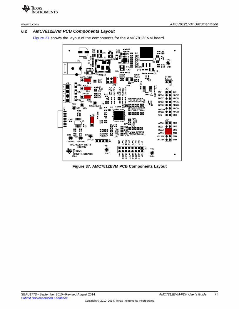
6.2 AMC7812EVM PCB Components LayoutFigure 37 shows the layout of the components for the AMC7812EVM board.
Figure 37. AMC7812EVM PCB Components Layout
25SBAU177D–September 2010–Revised August 2014 AMC7812EVM-PDK User’s GuideSubmit Documentation Feedback
Copyright © 2010–2014, Texas Instruments Incorporated
AMC7812EVM Documentation www.ti.com
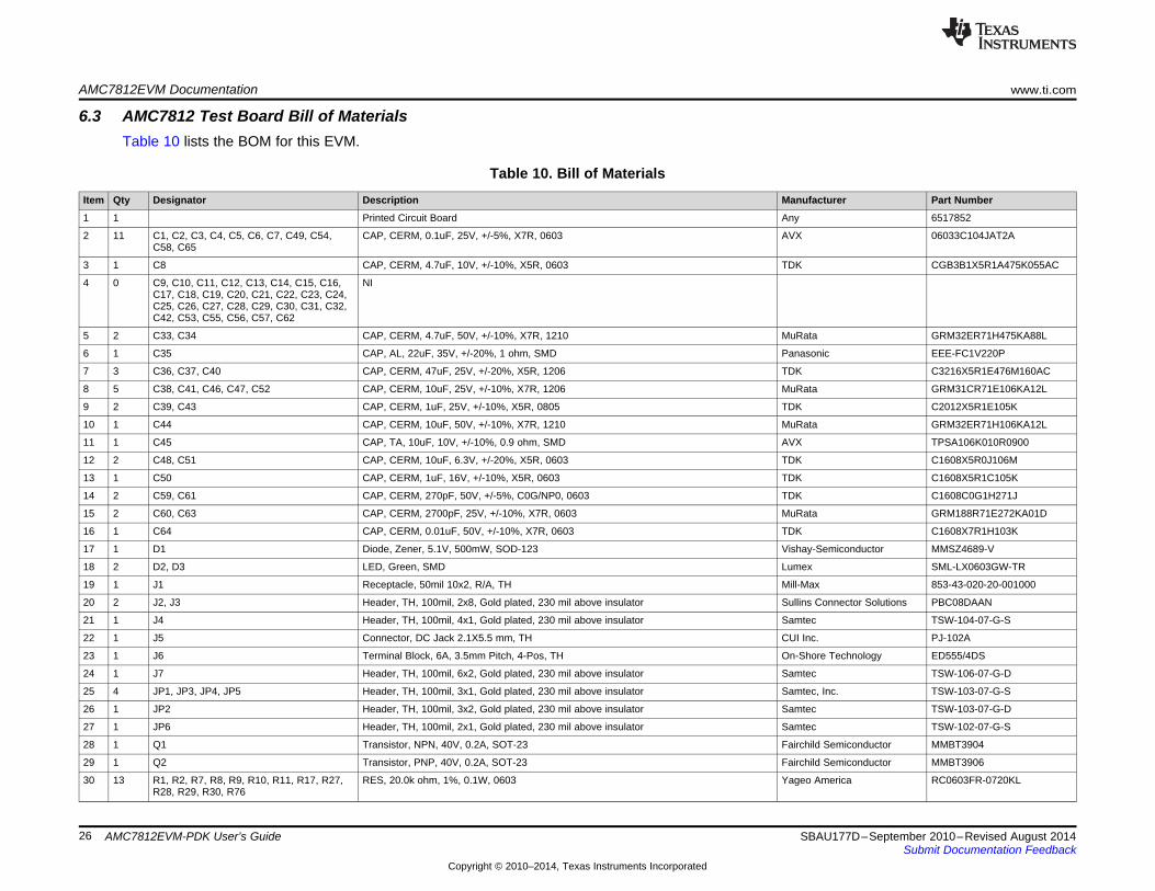
6.3 AMC7812 Test Board Bill of MaterialsTable 10 lists the BOM for this EVM.
Table 10. Bill of MaterialsItem Qty Designator Description Manufacturer Part Number
1 1 Printed Circuit Board Any 6517852
2 11 C1, C2, C3, C4, C5, C6, C7, C49, C54, CAP, CERM, 0.1uF, 25V, +/-5%, X7R, 0603 AVX 06033C104JAT2AC58, C65
3 1 C8 CAP, CERM, 4.7uF, 10V, +/-10%, X5R, 0603 TDK CGB3B1X5R1A475K055AC
4 0 C9, C10, C11, C12, C13, C14, C15, C16, NIC17, C18, C19, C20, C21, C22, C23, C24,C25, C26, C27, C28, C29, C30, C31, C32,C42, C53, C55, C56, C57, C62
5 2 C33, C34 CAP, CERM, 4.7uF, 50V, +/-10%, X7R, 1210 MuRata GRM32ER71H475KA88L
6 1 C35 CAP, AL, 22uF, 35V, +/-20%, 1 ohm, SMD Panasonic EEE-FC1V220P
7 3 C36, C37, C40 CAP, CERM, 47uF, 25V, +/-20%, X5R, 1206 TDK C3216X5R1E476M160AC
8 5 C38, C41, C46, C47, C52 CAP, CERM, 10uF, 25V, +/-10%, X7R, 1206 MuRata GRM31CR71E106KA12L
9 2 C39, C43 CAP, CERM, 1uF, 25V, +/-10%, X5R, 0805 TDK C2012X5R1E105K
10 1 C44 CAP, CERM, 10uF, 50V, +/-10%, X7R, 1210 MuRata GRM32ER71H106KA12L
11 1 C45 CAP, TA, 10uF, 10V, +/-10%, 0.9 ohm, SMD AVX TPSA106K010R0900
12 2 C48, C51 CAP, CERM, 10uF, 6.3V, +/-20%, X5R, 0603 TDK C1608X5R0J106M
13 1 C50 CAP, CERM, 1uF, 16V, +/-10%, X5R, 0603 TDK C1608X5R1C105K
14 2 C59, C61 CAP, CERM, 270pF, 50V, +/-5%, C0G/NP0, 0603 TDK C1608C0G1H271J
15 2 C60, C63 CAP, CERM, 2700pF, 25V, +/-10%, X7R, 0603 MuRata GRM188R71E272KA01D
16 1 C64 CAP, CERM, 0.01uF, 50V, +/-10%, X7R, 0603 TDK C1608X7R1H103K
17 1 D1 Diode, Zener, 5.1V, 500mW, SOD-123 Vishay-Semiconductor MMSZ4689-V
18 2 D2, D3 LED, Green, SMD Lumex SML-LX0603GW-TR
19 1 J1 Receptacle, 50mil 10x2, R/A, TH Mill-Max 853-43-020-20-001000
20 2 J2, J3 Header, TH, 100mil, 2x8, Gold plated, 230 mil above insulator Sullins Connector Solutions PBC08DAAN
21 1 J4 Header, TH, 100mil, 4x1, Gold plated, 230 mil above insulator Samtec TSW-104-07-G-S
22 1 J5 Connector, DC Jack 2.1X5.5 mm, TH CUI Inc. PJ-102A
23 1 J6 Terminal Block, 6A, 3.5mm Pitch, 4-Pos, TH On-Shore Technology ED555/4DS
24 1 J7 Header, TH, 100mil, 6x2, Gold plated, 230 mil above insulator Samtec TSW-106-07-G-D
25 4 JP1, JP3, JP4, JP5 Header, TH, 100mil, 3x1, Gold plated, 230 mil above insulator Samtec, Inc. TSW-103-07-G-S
26 1 JP2 Header, TH, 100mil, 3x2, Gold plated, 230 mil above insulator Samtec TSW-103-07-G-D
27 1 JP6 Header, TH, 100mil, 2x1, Gold plated, 230 mil above insulator Samtec TSW-102-07-G-S
28 1 Q1 Transistor, NPN, 40V, 0.2A, SOT-23 Fairchild Semiconductor MMBT3904
29 1 Q2 Transistor, PNP, 40V, 0.2A, SOT-23 Fairchild Semiconductor MMBT3906
30 13 R1, R2, R7, R8, R9, R10, R11, R17, R27, RES, 20.0k ohm, 1%, 0.1W, 0603 Yageo America RC0603FR-0720KLR28, R29, R30, R76
26 AMC7812EVM-PDK User’s Guide SBAU177D–September 2010–Revised August 2014Submit Documentation Feedback
Copyright © 2010–2014, Texas Instruments Incorporated
www.ti.com AMC7812EVM Documentation
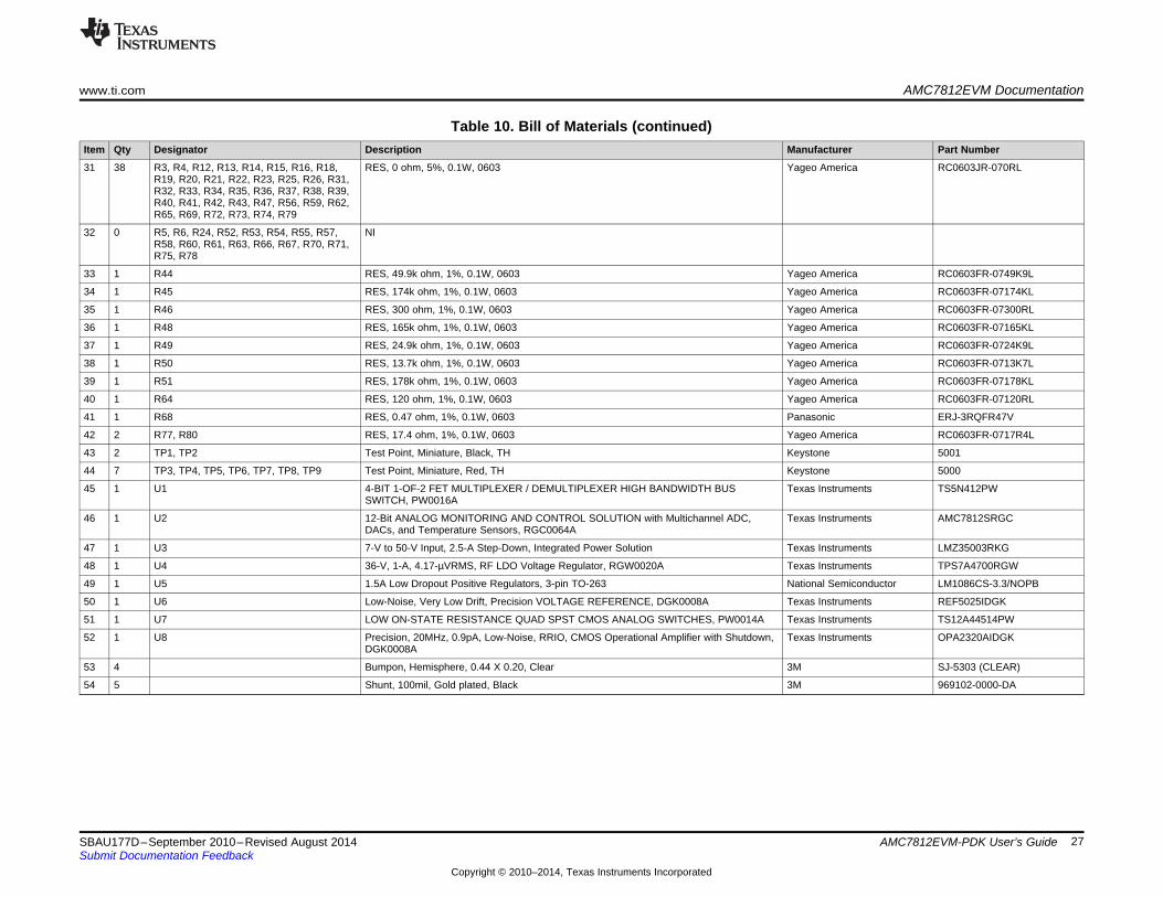
Table 10. Bill of Materials (continued)Item Qty Designator Description Manufacturer Part Number
31 38 R3, R4, R12, R13, R14, R15, R16, R18, RES, 0 ohm, 5%, 0.1W, 0603 Yageo America RC0603JR-070RLR19, R20, R21, R22, R23, R25, R26, R31,R32, R33, R34, R35, R36, R37, R38, R39,R40, R41, R42, R43, R47, R56, R59, R62,R65, R69, R72, R73, R74, R79
32 0 R5, R6, R24, R52, R53, R54, R55, R57, NIR58, R60, R61, R63, R66, R67, R70, R71,R75, R78
33 1 R44 RES, 49.9k ohm, 1%, 0.1W, 0603 Yageo America RC0603FR-0749K9L
34 1 R45 RES, 174k ohm, 1%, 0.1W, 0603 Yageo America RC0603FR-07174KL
35 1 R46 RES, 300 ohm, 1%, 0.1W, 0603 Yageo America RC0603FR-07300RL
36 1 R48 RES, 165k ohm, 1%, 0.1W, 0603 Yageo America RC0603FR-07165KL
37 1 R49 RES, 24.9k ohm, 1%, 0.1W, 0603 Yageo America RC0603FR-0724K9L
38 1 R50 RES, 13.7k ohm, 1%, 0.1W, 0603 Yageo America RC0603FR-0713K7L
39 1 R51 RES, 178k ohm, 1%, 0.1W, 0603 Yageo America RC0603FR-07178KL
40 1 R64 RES, 120 ohm, 1%, 0.1W, 0603 Yageo America RC0603FR-07120RL
41 1 R68 RES, 0.47 ohm, 1%, 0.1W, 0603 Panasonic ERJ-3RQFR47V
42 2 R77, R80 RES, 17.4 ohm, 1%, 0.1W, 0603 Yageo America RC0603FR-0717R4L
43 2 TP1, TP2 Test Point, Miniature, Black, TH Keystone 5001
44 7 TP3, TP4, TP5, TP6, TP7, TP8, TP9 Test Point, Miniature, Red, TH Keystone 5000
45 1 U1 4-BIT 1-OF-2 FET MULTIPLEXER / DEMULTIPLEXER HIGH BANDWIDTH BUS Texas Instruments TS5N412PWSWITCH, PW0016A
46 1 U2 12-Bit ANALOG MONITORING AND CONTROL SOLUTION with Multichannel ADC, Texas Instruments AMC7812SRGCDACs, and Temperature Sensors, RGC0064A
47 1 U3 7-V to 50-V Input, 2.5-A Step-Down, Integrated Power Solution Texas Instruments LMZ35003RKG
48 1 U4 36-V, 1-A, 4.17-µVRMS, RF LDO Voltage Regulator, RGW0020A Texas Instruments TPS7A4700RGW
49 1 U5 1.5A Low Dropout Positive Regulators, 3-pin TO-263 National Semiconductor LM1086CS-3.3/NOPB
50 1 U6 Low-Noise, Very Low Drift, Precision VOLTAGE REFERENCE, DGK0008A Texas Instruments REF5025IDGK
51 1 U7 LOW ON-STATE RESISTANCE QUAD SPST CMOS ANALOG SWITCHES, PW0014A Texas Instruments TS12A44514PW
52 1 U8 Precision, 20MHz, 0.9pA, Low-Noise, RRIO, CMOS Operational Amplifier with Shutdown, Texas Instruments OPA2320AIDGKDGK0008A
53 4 Bumpon, Hemisphere, 0.44 X 0.20, Clear 3M SJ-5303 (CLEAR)
54 5 Shunt, 100mil, Gold plated, Black 3M 969102-0000-DA
27SBAU177D–September 2010–Revised August 2014 AMC7812EVM-PDK User’s GuideSubmit Documentation Feedback
Copyright © 2010–2014, Texas Instruments Incorporated
Revision D History www.ti.com
Revision D History
Changes from C Revision (June 2014) to D Revision .................................................................................................... Page
• Updated JP1 jumper function description in Default Jumper Settings table....................................................... 9• Removed jumper table .................................................................................................................. 22
NOTE: Page numbers for previous revisions may differ from page numbers in the current version.
Revision C History
Changes from B Revision (June 2014) to C Revision .................................................................................................... Page
• Changed title of document to AMC7812EVM-PDK User’s Guide................................................................... 1
Revision B History
Changes from A Revision (May 2013) to B Revision ...................................................................................................... Page
• Changed entire document: format and content. This user guide is now patterned after the AMC7832EVM user's guide. . 1
28 Revision History SBAU177D–September 2010–Revised August 2014Submit Documentation Feedback
Copyright © 2010–2014, Texas Instruments Incorporated
ADDITIONAL TERMS AND CONDITIONS, WARNINGS, RESTRICTIONS, AND DISCLAIMERS FOREVALUATION MODULES
Texas Instruments Incorporated (TI) markets, sells, and loans all evaluation boards, kits, and/or modules (EVMs) pursuant to, and userexpressly acknowledges, represents, and agrees, and takes sole responsibility and risk with respect to, the following:
1. User agrees and acknowledges that EVMs are intended to be handled and used for feasibility evaluation only in laboratory and/ordevelopment environments. Notwithstanding the foregoing, in certain instances, TI makes certain EVMs available to users that do nothandle and use EVMs solely for feasibility evaluation only in laboratory and/or development environments, but may use EVMs in ahobbyist environment. All EVMs made available to hobbyist users are FCC certified, as applicable. Hobbyist users acknowledge, agree,and shall comply with all applicable terms, conditions, warnings, and restrictions in this document and are subject to the disclaimer andindemnity provisions included in this document.
2. Unless otherwise indicated, EVMs are not finished products and not intended for consumer use. EVMs are intended solely for use bytechnically qualified electronics experts who are familiar with the dangers and application risks associated with handling electricalmechanical components, systems, and subsystems.
3. User agrees that EVMs shall not be used as, or incorporated into, all or any part of a finished product.4. User agrees and acknowledges that certain EVMs may not be designed or manufactured by TI.5. User must read the user's guide and all other documentation accompanying EVMs, including without limitation any warning or
restriction notices, prior to handling and/or using EVMs. Such notices contain important safety information related to, for example,temperatures and voltages. For additional information on TI's environmental and/or safety programs, please visit www.ti.com/esh orcontact TI.
6. User assumes all responsibility, obligation, and any corresponding liability for proper and safe handling and use of EVMs.7. Should any EVM not meet the specifications indicated in the user’s guide or other documentation accompanying such EVM, the EVM
may be returned to TI within 30 days from the date of delivery for a full refund. THE FOREGOING LIMITED WARRANTY IS THEEXCLUSIVE WARRANTY MADE BY TI TO USER AND IS IN LIEU OF ALL OTHER WARRANTIES, EXPRESSED, IMPLIED, ORSTATUTORY, INCLUDING ANY WARRANTY OF MERCHANTABILITY OR FITNESS FOR ANY PARTICULAR PURPOSE. TI SHALLNOT BE LIABLE TO USER FOR ANY INDIRECT, SPECIAL, INCIDENTAL, OR CONSEQUENTIAL DAMAGES RELATED TO THEHANDLING OR USE OF ANY EVM.
8. No license is granted under any patent right or other intellectual property right of TI covering or relating to any machine, process, orcombination in which EVMs might be or are used. TI currently deals with a variety of customers, and therefore TI’s arrangement withthe user is not exclusive. TI assumes no liability for applications assistance, customer product design, software performance, orinfringement of patents or services with respect to the handling or use of EVMs.
9. User assumes sole responsibility to determine whether EVMs may be subject to any applicable federal, state, or local laws andregulatory requirements (including but not limited to U.S. Food and Drug Administration regulations, if applicable) related to its handlingand use of EVMs and, if applicable, compliance in all respects with such laws and regulations.
10. User has sole responsibility to ensure the safety of any activities to be conducted by it and its employees, affiliates, contractors ordesignees, with respect to handling and using EVMs. Further, user is responsible to ensure that any interfaces (electronic and/ormechanical) between EVMs and any human body are designed with suitable isolation and means to safely limit accessible leakagecurrents to minimize the risk of electrical shock hazard.
11. User shall employ reasonable safeguards to ensure that user’s use of EVMs will not result in any property damage, injury or death,even if EVMs should fail to perform as described or expected.
12. User shall be solely responsible for proper disposal and recycling of EVMs consistent with all applicable federal, state, and localrequirements.
Certain Instructions. User shall operate EVMs within TI’s recommended specifications and environmental considerations per the user’sguide, accompanying documentation, and any other applicable requirements. Exceeding the specified ratings (including but not limited toinput and output voltage, current, power, and environmental ranges) for EVMs may cause property damage, personal injury or death. Ifthere are questions concerning these ratings, user should contact a TI field representative prior to connecting interface electronics includinginput power and intended loads. Any loads applied outside of the specified output range may result in unintended and/or inaccurateoperation and/or possible permanent damage to the EVM and/or interface electronics. Please consult the applicable EVM user's guide priorto connecting any load to the EVM output. If there is uncertainty as to the load specification, please contact a TI field representative. Duringnormal operation, some circuit components may have case temperatures greater than 60°C as long as the input and output are maintainedat a normal ambient operating temperature. These components include but are not limited to linear regulators, switching transistors, passtransistors, and current sense resistors which can be identified using EVMs’ schematics located in the applicable EVM user's guide. Whenplacing measurement probes near EVMs during normal operation, please be aware that EVMs may become very warm. As with allelectronic evaluation tools, only qualified personnel knowledgeable in electronic measurement and diagnostics normally found indevelopment environments should use EVMs.Agreement to Defend, Indemnify and Hold Harmless. User agrees to defend, indemnify, and hold TI, its directors, officers, employees,agents, representatives, affiliates, licensors and their representatives harmless from and against any and all claims, damages, losses,expenses, costs and liabilities (collectively, "Claims") arising out of, or in connection with, any handling and/or use of EVMs. User’sindemnity shall apply whether Claims arise under law of tort or contract or any other legal theory, and even if EVMs fail to perform asdescribed or expected.Safety-Critical or Life-Critical Applications. If user intends to use EVMs in evaluations of safety critical applications (such as life support),and a failure of a TI product considered for purchase by user for use in user’s product would reasonably be expected to cause severepersonal injury or death such as devices which are classified as FDA Class III or similar classification, then user must specifically notify TIof such intent and enter into a separate Assurance and Indemnity Agreement.
RADIO FREQUENCY REGULATORY COMPLIANCE INFORMATION FOR EVALUATION MODULESTexas Instruments Incorporated (TI) evaluation boards, kits, and/or modules (EVMs) and/or accompanying hardware that is marketed, sold,or loaned to users may or may not be subject to radio frequency regulations in specific countries.General Statement for EVMs Not Including a RadioFor EVMs not including a radio and not subject to the U.S. Federal Communications Commission (FCC) or Industry Canada (IC)regulations, TI intends EVMs to be used only for engineering development, demonstration, or evaluation purposes. EVMs are not finishedproducts typically fit for general consumer use. EVMs may nonetheless generate, use, or radiate radio frequency energy, but have not beentested for compliance with the limits of computing devices pursuant to part 15 of FCC or the ICES-003 rules. Operation of such EVMs maycause interference with radio communications, in which case the user at his own expense will be required to take whatever measures maybe required to correct this interference.General Statement for EVMs including a radioUser Power/Frequency Use Obligations: For EVMs including a radio, the radio included in such EVMs is intended for development and/orprofessional use only in legally allocated frequency and power limits. Any use of radio frequencies and/or power availability in such EVMsand their development application(s) must comply with local laws governing radio spectrum allocation and power limits for such EVMs. It isthe user’s sole responsibility to only operate this radio in legally acceptable frequency space and within legally mandated power limitations.Any exceptions to this are strictly prohibited and unauthorized by TI unless user has obtained appropriate experimental and/or developmentlicenses from local regulatory authorities, which is the sole responsibility of the user, including its acceptable authorization.
U.S. Federal Communications Commission Compliance
For EVMs Annotated as FCC – FEDERAL COMMUNICATIONS COMMISSION Part 15 Compliant
CautionThis device complies with part 15 of the FCC Rules. Operation is subject to the following two conditions: (1) This device may not causeharmful interference, and (2) this device must accept any interference received, including interference that may cause undesired operation.Changes or modifications could void the user's authority to operate the equipment.
FCC Interference Statement for Class A EVM devicesThis equipment has been tested and found to comply with the limits for a Class A digital device, pursuant to part 15 of the FCC Rules.These limits are designed to provide reasonable protection against harmful interference when the equipment is operated in a commercialenvironment. This equipment generates, uses, and can radiate radio frequency energy and, if not installed and used in accordance with theinstruction manual, may cause harmful interference to radio communications. Operation of this equipment in a residential area is likely tocause harmful interference in which case the user will be required to correct the interference at its own expense.
FCC Interference Statement for Class B EVM devicesThis equipment has been tested and found to comply with the limits for a Class B digital device, pursuant to part 15 of the FCC Rules.These limits are designed to provide reasonable protection against harmful interference in a residential installation. This equipmentgenerates, uses and can radiate radio frequency energy and, if not installed and used in accordance with the instructions, may causeharmful interference to radio communications. However, there is no guarantee that interference will not occur in a particular installation. Ifthis equipment does cause harmful interference to radio or television reception, which can be determined by turning the equipment off andon, the user is encouraged to try to correct the interference by one or more of the following measures:
• Reorient or relocate the receiving antenna.• Increase the separation between the equipment and receiver.• Connect the equipment into an outlet on a circuit different from that to which the receiver is connected.• Consult the dealer or an experienced radio/TV technician for help.
Industry Canada Compliance (English)For EVMs Annotated as IC – INDUSTRY CANADA Compliant:
This Class A or B digital apparatus complies with Canadian ICES-003.Changes or modifications not expressly approved by the party responsible for compliance could void the user’s authority to operate theequipment.
Concerning EVMs Including Radio TransmittersThis device complies with Industry Canada licence-exempt RSS standard(s). Operation is subject to the following two conditions: (1) thisdevice may not cause interference, and (2) this device must accept any interference, including interference that may cause undesiredoperation of the device.
Concerning EVMs Including Detachable AntennasUnder Industry Canada regulations, this radio transmitter may only operate using an antenna of a type and maximum (or lesser) gainapproved for the transmitter by Industry Canada. To reduce potential radio interference to other users, the antenna type and its gain shouldbe so chosen that the equivalent isotropically radiated power (e.i.r.p.) is not more than that necessary for successful communication.This radio transmitter has been approved by Industry Canada to operate with the antenna types listed in the user guide with the maximumpermissible gain and required antenna impedance for each antenna type indicated. Antenna types not included in this list, having a gaingreater than the maximum gain indicated for that type, are strictly prohibited for use with this device.
Canada Industry Canada Compliance (French)
Cet appareil numérique de la classe A ou B est conforme à la norme NMB-003 du Canada
Les changements ou les modifications pas expressément approuvés par la partie responsable de la conformité ont pu vider l’autorité del'utilisateur pour actionner l'équipement.
Concernant les EVMs avec appareils radio
Le présent appareil est conforme aux CNR d'Industrie Canada applicables aux appareils radio exempts de licence. L'exploitation estautorisée aux deux conditions suivantes : (1) l'appareil ne doit pas produire de brouillage, et (2) l'utilisateur de l'appareil doit accepter toutbrouillage radioélectrique subi, même si le brouillage est susceptible d'en compromettre le fonctionnement.
Concernant les EVMs avec antennes détachables
Conformément à la réglementation d'Industrie Canada, le présent émetteur radio peut fonctionner avec une antenne d'un type et d'un gainmaximal (ou inférieur) approuvé pour l'émetteur par Industrie Canada. Dans le but de réduire les risques de brouillage radioélectrique àl'intention des autres utilisateurs, il faut choisir le type d'antenne et son gain de sorte que la puissance isotrope rayonnée équivalente(p.i.r.e.) ne dépasse pas l'intensité nécessaire à l'établissement d'une communication satisfaisante.
Le présent émetteur radio a été approuvé par Industrie Canada pour fonctionner avec les types d'antenne énumérés dans le manueld’usage et ayant un gain admissible maximal et l'impédance requise pour chaque type d'antenne. Les types d'antenne non inclus danscette liste, ou dont le gain est supérieur au gain maximal indiqué, sont strictement interdits pour l'exploitation de l'émetteur.
Mailing Address: Texas Instruments, Post Office Box 655303, Dallas, Texas 75265Copyright © 2014, Texas Instruments Incorporated
spacer
Important Notice for Users of EVMs Considered “Radio Frequency Products” in JapanEVMs entering Japan are NOT certified by TI as conforming to Technical Regulations of Radio Law of Japan.
If user uses EVMs in Japan, user is required by Radio Law of Japan to follow the instructions below with respect to EVMs:1. Use EVMs in a shielded room or any other test facility as defined in the notification #173 issued by Ministry of Internal Affairs and
Communications on March 28, 2006, based on Sub-section 1.1 of Article 6 of the Ministry’s Rule for Enforcement of Radio Law ofJapan,
2. Use EVMs only after user obtains the license of Test Radio Station as provided in Radio Law of Japan with respect to EVMs, or3. Use of EVMs only after user obtains the Technical Regulations Conformity Certification as provided in Radio Law of Japan with respect
to EVMs. Also, do not transfer EVMs, unless user gives the same notice above to the transferee. Please note that if user does notfollow the instructions above, user will be subject to penalties of Radio Law of Japan.
http://www.tij.co.jp
【無線電波を送信する製品の開発キットをお使いになる際の注意事項】 本開発キットは技術基準適合証明を受けておりません。 本製品のご使用に際しては、電波法遵守のため、以下のいずれかの措置を取っていただく必要がありますのでご注意ください。
1. 電波法施行規則第6条第1項第1号に基づく平成18年3月28日総務省告示第173号で定められた電波暗室等の試験設備でご使用いただく。2. 実験局の免許を取得後ご使用いただく。3. 技術基準適合証明を取得後ご使用いただく。。
なお、本製品は、上記の「ご使用にあたっての注意」を譲渡先、移転先に通知しない限り、譲渡、移転できないものとします
上記を遵守頂けない場合は、電波法の罰則が適用される可能性があることをご留意ください。
日本テキサス・インスツルメンツ株式会社東京都新宿区西新宿6丁目24番1号西新宿三井ビルhttp://www.tij.co.jp
Texas Instruments Japan Limited(address) 24-1, Nishi-Shinjuku 6 chome, Shinjuku-ku, Tokyo, Japan

IMPORTANT NOTICETexas Instruments Incorporated and its subsidiaries (TI) reserve the right to make corrections, enhancements, improvements and otherchanges to its semiconductor products and services per JESD46, latest issue, and to discontinue any product or service per JESD48, latestissue. Buyers should obtain the latest relevant information before placing orders and should verify that such information is current andcomplete. All semiconductor products (also referred to herein as “components”) are sold subject to TI’s terms and conditions of salesupplied at the time of order acknowledgment.TI warrants performance of its components to the specifications applicable at the time of sale, in accordance with the warranty in TI’s termsand conditions of sale of semiconductor products. Testing and other quality control techniques are used to the extent TI deems necessaryto support this warranty. Except where mandated by applicable law, testing of all parameters of each component is not necessarilyperformed.TI assumes no liability for applications assistance or the design of Buyers’ products. Buyers are responsible for their products andapplications using TI components. To minimize the risks associated with Buyers’ products and applications, Buyers should provideadequate design and operating safeguards.TI does not warrant or represent that any license, either express or implied, is granted under any patent right, copyright, mask work right, orother intellectual property right relating to any combination, machine, or process in which TI components or services are used. Informationpublished by TI regarding third-party products or services does not constitute a license to use such products or services or a warranty orendorsement thereof. Use of such information may require a license from a third party under the patents or other intellectual property of thethird party, or a license from TI under the patents or other intellectual property of TI.Reproduction of significant portions of TI information in TI data books or data sheets is permissible only if reproduction is without alterationand is accompanied by all associated warranties, conditions, limitations, and notices. TI is not responsible or liable for such altereddocumentation. Information of third parties may be subject to additional restrictions.Resale of TI components or services with statements different from or beyond the parameters stated by TI for that component or servicevoids all express and any implied warranties for the associated TI component or service and is an unfair and deceptive business practice.TI is not responsible or liable for any such statements.Buyer acknowledges and agrees that it is solely responsible for compliance with all legal, regulatory and safety-related requirementsconcerning its products, and any use of TI components in its applications, notwithstanding any applications-related information or supportthat may be provided by TI. Buyer represents and agrees that it has all the necessary expertise to create and implement safeguards whichanticipate dangerous consequences of failures, monitor failures and their consequences, lessen the likelihood of failures that might causeharm and take appropriate remedial actions. Buyer will fully indemnify TI and its representatives against any damages arising out of the useof any TI components in safety-critical applications.In some cases, TI components may be promoted specifically to facilitate safety-related applications. With such components, TI’s goal is tohelp enable customers to design and create their own end-product solutions that meet applicable functional safety standards andrequirements. Nonetheless, such components are subject to these terms.No TI components are authorized for use in FDA Class III (or similar life-critical medical equipment) unless authorized officers of the partieshave executed a special agreement specifically governing such use.Only those TI components which TI has specifically designated as military grade or “enhanced plastic” are designed and intended for use inmilitary/aerospace applications or environments. Buyer acknowledges and agrees that any military or aerospace use of TI componentswhich have not been so designated is solely at the Buyer's risk, and that Buyer is solely responsible for compliance with all legal andregulatory requirements in connection with such use.TI has specifically designated certain components as meeting ISO/TS16949 requirements, mainly for automotive use. In any case of use ofnon-designated products, TI will not be responsible for any failure to meet ISO/TS16949.Products ApplicationsAudio www.ti.com/audio Automotive and Transportation www.ti.com/automotiveAmplifiers amplifier.ti.com Communications and Telecom www.ti.com/communicationsData Converters dataconverter.ti.com Computers and Peripherals www.ti.com/computersDLP® Products www.dlp.com Consumer Electronics www.ti.com/consumer-appsDSP dsp.ti.com Energy and Lighting www.ti.com/energyClocks and Timers www.ti.com/clocks Industrial www.ti.com/industrialInterface interface.ti.com Medical www.ti.com/medicalLogic logic.ti.com Security www.ti.com/securityPower Mgmt power.ti.com Space, Avionics and Defense www.ti.com/space-avionics-defenseMicrocontrollers microcontroller.ti.com Video and Imaging www.ti.com/videoRFID www.ti-rfid.comOMAP Applications Processors www.ti.com/omap TI E2E Community e2e.ti.comWireless Connectivity www.ti.com/wirelessconnectivity
Mailing Address: Texas Instruments, Post Office Box 655303, Dallas, Texas 75265Copyright © 2014, Texas Instruments Incorporated