Embed Size (px)
Citation preview

Frequency (MHz)
Am
plitu
de (
dBF
S)
0 12.5 25 37.5 50 62.5-120
-110
-100
-90
-80
-70
-60
-50
-40
-30
-20
-10
0
D201
Product
Folder
Sample &Buy
Technical
Documents
Tools &
Software
Support &Community
ADC3421, ADC3422, ADC3423, ADC3424SBAS673A –JULY 2014–REVISED OCTOBER 2015
ADC342x Quad-Channel, 12-Bit, 25-MSPS to 125-MSPS, Analog-to-Digital Converter1 Features 3 Description
The ADC342x are a high-linearity, ultra-low power,1• Quad Channel
quad-channel, 12-bit, 25-MSPS to 125-MSPS,• 12-Bit Resolution analog-to-digital converter (ADC) family. The devices• Single Supply: 1.8 V are designed specifically to support demanding, high
input frequency signals with large dynamic range• Serial LVDS Interfacerequirements. An input clock divider allows more• Flexible Input Clock Buffer with Divide-by-1, -2, -4 flexibility for system clock architecture design and the
• SNR = 70.2 dBFS, SFDR = 87 dBc at SYSREF input enables complete systemfIN = 70 MHz synchronization. The ADC342x family supports serial
low-voltage differential signaling (LVDS) in order to• Ultra-Low Power Consumption:reduce the number of interface lines, thus allowing for– 98 mW/Ch at 125 MSPS high system integration density. The serial LVDS
• Channel Isolation: 105 dB interface is two-wire, where each ADC data are• Internal Dither and Chopper serialized and output over two LVDS pairs. An
internal phase-locked loop (PLL) multiplies the• Support for Multi-Chip Synchronizationincoming ADC sampling clock to derive the bit clock• Pin-to-Pin Compatible with 14-Bit Version that is used to serialize the 12-bit output data from
• Package: VQFN-56 (8 mm × 8 mm) each channel. In addition to the serial data streams,the frame and bit clocks are also transmitted asLVDS outputs.2 Applications
• Multi-Carrier, Multi-Mode Cellular Base Stations Device Information(1)
• Radar and Smart Antenna Arrays PART NUMBER PACKAGE BODY SIZE (NOM)• Munitions Guidance ADC342x VQFN (56) 8.00 mm × 8.00 mm• Motor Control Feedback (1) For all available packages, see the orderable addendum at
the end of the datasheet.• Network and Vector Analyzers• Communications Test Equipment space• Nondestructive Testing space• Microwave Receivers
space• Software-Defined Radios (SDRs)
space• Quadrature and Diversity Radio Receiversspace
space
Spectrum at 10-MHz IF(SFDR = 97 dBc, SNR = 70.4 dBFS, SINAD = 70.4 dBFS,
THD = 98 dBc, HD2 = 95 dBc, HD3 = 97 dBc)
1
An IMPORTANT NOTICE at the end of this data sheet addresses availability, warranty, changes, use in safety-critical applications,intellectual property matters and other important disclaimers. PRODUCTION DATA.

ADC3421, ADC3422, ADC3423, ADC3424SBAS673A –JULY 2014–REVISED OCTOBER 2015 www.ti.com
Table of Contents7.19 Typical Characteristics: Common ......................... 381 Features .................................................................. 17.20 Typical Characteristics: Contour ........................... 392 Applications ........................................................... 1
8 Parameter Measurement Information ................ 393 Description ............................................................. 18.1 Timing Diagrams..................................................... 394 Revision History..................................................... 2
9 Detailed Description ............................................ 415 Device Comparison Table ..................................... 39.1 Overview ................................................................. 416 Pin Configuration and Functions ......................... 39.2 Functional Block Diagram ....................................... 417 Specifications......................................................... 59.3 Feature Description................................................. 427.1 Absolute Maximum Ratings ...................................... 59.4 Device Functional Modes........................................ 467.2 ESD Ratings.............................................................. 59.5 Programming........................................................... 477.3 Recommended Operating Conditions....................... 59.6 Register Maps ......................................................... 517.4 Thermal Information .................................................. 6
10 Applications and Implementation...................... 667.5 Electrical Characteristics: General ............................ 610.1 Application Information.......................................... 667.6 Electrical Characteristics: ADC3421, ADC3422 ....... 710.2 Typical Applications .............................................. 677.7 Electrical Characteristics: ADC3423, ADC3424 ....... 7
11 Power Supply Recommendations ..................... 697.8 AC Performance: ADC3421...................................... 812 Layout................................................................... 707.9 AC Performance: ADC3422.................................... 10
12.1 Layout Guidelines ................................................. 707.10 AC Performance: ADC3423.................................. 1212.2 Layout Example .................................................... 707.11 AC Performance: ADC3424.................................. 14
13 Device and Documentation Support ................. 717.12 Digital Characteristics ........................................... 1613.1 Related Links ........................................................ 717.13 Timing Requirements: General ............................. 1613.2 Community Resources.......................................... 717.14 Timing Requirements: LVDS Output..................... 1713.3 Trademarks ........................................................... 717.15 Typical Characteristics: ADC3421 ........................ 1813.4 Electrostatic Discharge Caution............................ 717.16 Typical Characteristics: ADC3422 ........................ 2313.5 Glossary ................................................................ 717.17 Typical Characteristics: ADC3423 ........................ 28
7.18 Typical Characteristics: ADC3424 ........................ 33 14 Mechanical, Packaging, and OrderableInformation ........................................................... 71
4 Revision HistoryNOTE: Page numbers for previous revisions may differ from page numbers in the current version.
Changes from Original (July 2014) to Revision A Page
• Released to production........................................................................................................................................................... 1
2 Submit Documentation Feedback Copyright © 2014–2015, Texas Instruments Incorporated
Product Folder Links: ADC3421 ADC3422 ADC3423 ADC3424

1
2
3
4
5
6
7
8
9
10
11
12
13
14
15 16 17 18 19 20 21 22 23 24 25 26 27 28
42
41
40
39
38
37
36
35
34
33
32
31
30
29
56 55 54 53 52 51 50 49 48 47 46 45 44 43D
CLK
P
DV
DD
DB
0M
DB
0P
CLK
P
SD
OU
T
AV
DD
DA1P
DC
0P
DC
0MS
YS
RE
FP
DVDD
DA0M
AVDD
AVDD
INAM
INBM
AVDD
INAP
GND Pad
(Back Side)
DD0M
DD1M
DD1P
DC
1P
DC
1M
DV
DD
FC
LKP
FC
LKM
DD0P
DVDD
PDN
AVDD
INDM
INDP
AVDD
INCP
AVDD
INCM
AVDD
AV
DD
VC
M
SY
SR
EF
M
RE
SE
T
AV
DD
CLK
M
SD
AT
A
AV
DD
SC
LK
SE
N
DB
1M
DC
LKM
DB
1P
DA1M
DA0P
AVDD
INBP
AVDD
ADC3421, ADC3422, ADC3423, ADC3424www.ti.com SBAS673A –JULY 2014–REVISED OCTOBER 2015
5 Device Comparison Table
RESOLUTIONINTERFACE (Bits) 25 MSPS 50 MSPS 80 MSPS 125 MSPS 160 MSPS
12 ADC3421 ADC3422 ADC3423 ADC3424 —Serial LVDS
14 ADC3441 ADC3442 ADC3443 ADC3444 —12 — ADC34J22 ADC34J23 ADC34J24 ADC34J25
JESD204B14 — ADC34J42 ADC34J43 ADC34J44 ADC34J45
6 Pin Configuration and Functions
RTQ PackageVQFN-56Top View
Copyright © 2014–2015, Texas Instruments Incorporated Submit Documentation Feedback 3
Product Folder Links: ADC3421 ADC3422 ADC3423 ADC3424

ADC3421, ADC3422, ADC3423, ADC3424SBAS673A –JULY 2014–REVISED OCTOBER 2015 www.ti.com
Pin FunctionsPIN
I/O DESCRIPTIONNAME NO.
6, 7, 10, 11, 14,AVDD 15, 20, 23, 28, 29, I Analog 1.8-V power supply
32, 33, 36CLKM 21 I Negative differential clock input for the ADCCLKP 22 I Positive differential clock input for the ADCDA0M 4 O Negative serial LVDS output for wire-0 of channel ADA0P 3 O Positive serial LVDS output for wire-0 of channel ADA1M 2 O Negative serial LVDS output for wire-1 of channel ADA1P 1 O Positive serial LVDS output for wire-1 of channel ADB0M 56 O Negative serial LVDS output for wire-0 of channel BDB0P 55 O Positive serial LVDS output for wire-0 of channel BDB1M 54 O Negative serial LVDS output for wire-1 of channel BDB1P 53 O Positive serial LVDS output for wire-1 of channel BDC0M 46 O Negative serial LVDS output for wire-0 of channel CDC0P 45 O Positive serial LVDS output for wire-0 of channel CDC1M 44 O Negative serial LVDS output for wire-1 of channel CDC1P 43 O Positive serial LVDS output for wire-1 of channel CDD0M 42 O Negative serial LVDS output for wire-0 of channel DDD0P 41 O Positive serial LVDS output for wire-0 of channel DDD1M 40 O Negative serial LVDS output for wire-1 of channel DDD1P 39 O Positive serial LVDS output for wire-1 of channel DDCLKM 51 O Negative bit clock outputDCLKP 50 O Positive bit clock outputDVDD 5, 38, 47, 52 I Digital 1.8-V power supplyFCLKM 49 O Negative frame clock outputFCLKP 48 O Positive frame clock outputGND PowerPAD™ I Ground, 0 VINAM 8 I Negative differential analog input for channel AINAP 9 I Positive differential analog input for channel AINBM 13 I Negative differential analog input for channel BINBP 12 I Positive differential analog input for channel BINCM 30 I Negative differential analog input for channel CINCP 31 I Positive differential analog input for channel CINDM 35 I Negative differential analog input for channel DINDP 34 I Positive differential analog input for channel D
Power-down control. This pin can be configured via the SPI. This pin has an internalPDN 37 I 150-kΩ pulldown resistor.RESET 24 I Hardware reset; active high. This pin has an internal 150-kΩ pulldown resistor.SCLK 16 I Serial interface clock input. This pin has an internal 150-kΩ pulldown resistor.SDATA 17 I Serial interface data input. This pin has an internal 150-kΩ pulldown resistor.SDOUT 19 O Serial interface data output
Serial interface enable; active low.SEN 18 I This pin has an internal 150-kΩ pullup resistor to AVDD.SYSREFM 26 I Negative external SYSREF inputSYSREFP 25 I Positive external SYSREF inputVCM 27 O Common-mode voltage for analog inputs
4 Submit Documentation Feedback Copyright © 2014–2015, Texas Instruments Incorporated
Product Folder Links: ADC3421 ADC3422 ADC3423 ADC3424

ADC3421, ADC3422, ADC3423, ADC3424www.ti.com SBAS673A –JULY 2014–REVISED OCTOBER 2015
7 Specifications
7.1 Absolute Maximum Ratingsover operating free-air temperature range (unless otherwise noted) (1)
MIN MAX UNITAnalog supply voltage range, AVDD –0.3 2.1 VDigital supply voltage range, DVDD –0.3 2.1 V
INAP, INBP, INCP, INDP, INAM, INBM, INCM, INDM –0.3 min (1.9, AVDD + 0.3)CLKP, CLKM –0.3 AVDD + 0.3Voltage applied to Vinput pins SYSREFP, SYSREFM –0.3 AVDD + 0.3SCLK, SEN, SDATA, RESET, PDN –0.3 3.9Operating free-air, TA –40 85
Temperature Operating junction, TJ 125 ºCStorage, Tstg –65 150
(1) Stresses beyond those listed under Absolute Maximum Ratings may cause permanent damage to the device. These are stress ratingsonly, which do not imply functional operation of the device at these or any other conditions beyond those indicated under RecommendedOperating Conditions. Exposure to absolute-maximum-rated conditions for extended periods may affect device reliability.
7.2 ESD RatingsVALUE UNIT
V(ESD) Electrostatic discharge Human body model (HBM), per ANSI/ESDA/JEDEC JS-001 (1) ±2000 V
(1) JEDEC document JEP155 states that 500-V HBM allows safe manufacturing with a standard ESD control process.
7.3 Recommended Operating Conditions (1)
over operating free-air temperature range (unless otherwise noted)MIN NOM MAX UNIT
SUPPLIESAVDD Analog supply voltage range 1.7 1.8 1.9 VDVDD Digital supply voltage range 1.7 1.8 1.9 VANALOG INPUT
For input frequencies < 450 MHz 2VID Differential input voltage VPPFor input frequencies < 600 MHz 1VIC Input common-mode voltage VCM ± 0.025 VCLOCK INPUT
Input clock frequency Sampling clock frequency 15 (2) 125 (3) MSPSSine wave, ac-coupled 0.2 1.5
Input clock amplitude (differential) LPECL, ac-coupled 1.6 VPP
LVDS, ac-coupled 0.7Input clock duty cycle 35% 50% 65%Input clock common-mode voltage 0.95 V
DIGITAL OUTPUTSMaximum external load capacitanceCLOAD 3.3 pFfrom each output pin to GND
RLOAD Single-ended load resistance 100 Ω
(1) After power-up, use only the RESET pin to reset the device for the first time; see the Register Initialization section for details.(2) See Table 3 for details.(3) With the clock divider enabled by default for divide-by-1. Maximum sampling clock frequency for the divide-by-4 option is 500 MSPS.
Copyright © 2014–2015, Texas Instruments Incorporated Submit Documentation Feedback 5
Product Folder Links: ADC3421 ADC3422 ADC3423 ADC3424

ADC3421, ADC3422, ADC3423, ADC3424SBAS673A –JULY 2014–REVISED OCTOBER 2015 www.ti.com
7.4 Thermal InformationADC342x
THERMAL METRIC (1) RTQ (VQFN) UNIT56 PINS
RθJA Junction-to-ambient thermal resistance 25.3 °C/WRθJC(top) Junction-to-case (top) thermal resistance 9.5 °C/WRθJB Junction-to-board thermal resistance 3.4 °C/WψJT Junction-to-top characterization parameter 0.2 °C/WψJB Junction-to-board characterization parameter 3.3 °C/WRθJC(bot) Junction-to-case (bottom) thermal resistance 0.5 °C/W
(1) For more information about traditional and new thermal metrics, see the IC Package Thermal Metrics application report, SPRA953.
7.5 Electrical Characteristics: GeneralTypical values are over the operating free-air temperature range, at TA = 25°C, full temperature range is TMIN = –40°C to TMAX= 85°C, maximum sampling rate, 50% clock duty cycle, AVDD = DVDD = 1.8 V, and –1-dBFS differential input, unlessotherwise noted.
PARAMETER TEST CONDITIONS MIN TYP MAX UNIT
ANALOG INPUT
Differential input full-scale 2.0 VPP
ri Input resistance Differential at dc 6.6 kΩ
ci Input capacitance Differential at dc 3.7 pF
VOC(VCM) VCM common-mode voltage output 0.95 V
VCM output current capability 10 mA
Input common-mode current Per analog input pin 1.5 µA/MSPS
50-Ω differential source driving 50-Ω terminationAnalog input bandwidth (3 dB) 540 MHzacross INP and INM
DC ACCURACY
EO Offset error –25 25 mV
αEO Temperature coefficient of offset error ± 0.024 mV/°C
Gain error as a result of internalEG(REF) –2 2 %FSreference inaccuracy alone
EG(CHAN) Gain error of channel alone –2 %FS
α(EGCHAN) Temperature coefficient of EG(CHAN) ±0.008 Δ%FS/Ch
CHANNEL-TO-CHANNEL ISOLATION
Near channel 105fIN = 10 MHz
Far channel 105
Near channel 95fIN = 100 MHz
Far channel 105
Near channel 94Crosstalk (1) fIN = 200 MHz dB
Far channel 105
Near channel 92fIN = 230 MHz
Far channel 105
Near channel 85fIN = 300 MHz
Far channel 105
(1) Crosstalk is measured with a –1-dBFS input signal on the aggressor channel and no input on the victim channel.
6 Submit Documentation Feedback Copyright © 2014–2015, Texas Instruments Incorporated
Product Folder Links: ADC3421 ADC3422 ADC3423 ADC3424

ADC3421, ADC3422, ADC3423, ADC3424www.ti.com SBAS673A –JULY 2014–REVISED OCTOBER 2015
7.6 Electrical Characteristics: ADC3421, ADC3422Typical values are over the operating free-air temperature range, at TA = 25°C, full temperature range is TMIN = –40°C to TMAX= 85°C, maximum sampling rate, 50% clock duty cycle, AVDD = DVDD = 1.8 V, and –1-dBFS differential input, unlessotherwise noted.
ADC3421 ADC3422PARAMETER MIN TYP MAX MIN TYP MAX UNIT
ADC clock frequency 25 50 MSPSResolution 12 12 Bits1.8-V analog supply current 54 71 71 90 mA1.8-V digital supply current 45 71 56 90 mATotal power dissipation 177 240 228 305 mWGlobal power-down dissipation 5 17 5 17 mWStandby power-down dissipation 34 75 35 75 mW
7.7 Electrical Characteristics: ADC3423, ADC3424Typical values are over the operating free-air temperature range, at TA = 25°C, full temperature range is TMIN = –40°C to TMAX= 85°C, maximum sampling rate, 50% clock duty cycle, AVDD = DVDD = 1.8 V, and –1-dBFS differential input, unlessotherwise noted.
ADC3423 ADC3424PARAMETER MIN TYP MAX MIN TYP MAX UNIT
ADC clock frequency 80 125 MSPSResolution 12 12 Bits1.8-V analog supply current 92 107 119 145 mA1.8-V digital supply current 68 100 98 145 mATotal power dissipation 288 365 391 475 mWGlobal power-down dissipation 5 17 5 17 mWStandby power-down dissipation 40 88 43 103 mW
Copyright © 2014–2015, Texas Instruments Incorporated Submit Documentation Feedback 7
Product Folder Links: ADC3421 ADC3422 ADC3423 ADC3424

ADC3421, ADC3422, ADC3423, ADC3424SBAS673A –JULY 2014–REVISED OCTOBER 2015 www.ti.com
7.8 AC Performance: ADC3421Typical values are over the operating free-air temperature range, at TA = 25°C, full temperature range is TMIN = –40°C to TMAX= 85°C, ADC sampling rate = 25 MSPS, 50% clock duty cycle, AVDD = DVDD = 1.8 V, and –1-dBFS differential input, unlessotherwise noted.
ADC3421 (fS = 25 MSPS)DITHER ON DITHER OFF
PARAMETER TEST CONDITIONS MIN TYP MAX MIN TYP MAX UNITfIN = 10 MHz 70.9 71.1fIN = 20 MHz 68.9 70.7 70.9fIN = 70 MHz 70.4 70.6Signal-to-noise ratio dBFS(from 1-MHz offset) fIN = 100 MHz 70.3 70.5fIN = 170 MHz 69.7 69.9fIN = 230 MHz 68.9 69.1
SNRfIN = 10 MHz 70.2 70.5fIN = 20 MHz 70.1 70.3fIN = 70 MHz 69.8 70.0Signal-to-noise ratio dBFS(full Nyquist band) fIN = 100 MHz 69.6 69.8fIN = 170 MHz 69.2 69.3fIN = 230 MHz 68.3 68.5fIN = 10 MHz –141.5 –141.7fIN = 20 MHz –141.3 –139.5 –141.5fIN = 70 MHz –141.0 –141.2Noise spectral densityNSD (1) dBFS/Hz(averaged across Nyquist zone) fIN = 100 MHz –140.9 –141.1fIN = 170 MHz –140.3 –140.5fIN = 230 MHz –139.5 –139.7fIN = 10 MHz 71 71.1fIN = 20 MHz 67.9 70.8 70.9fIN = 70 MHz 69.5 70Signal-to-noise and distortionSINAD (1) dBFSratio fIN = 100 MHz 70.5 70.7fIN = 170 MHz 69.6 69.8fIN = 230 MHz 68.7 68.7fIN = 10 MHz 11.5 11.5fIN = 20 MHz 11 11.4 11.4fIN = 70 MHz 11.4 11.4
ENOB (1) Effective number of bits BitsfIN = 100 MHz 11.4 11.4fIN = 170 MHz 11.3 11.3fIN = 230 MHz 11.1 11.1fIN = 10 MHz 93 90fIN = 20 MHz 84 91 85fIN = 70 MHz 93 88
SFDR Spurious-free dynamic range dBcfIN = 100 MHz 85 82fIN = 170 MHz 86 85fIN = 230 MHz 82 82
(1) Reported from a 1-MHz offset.
8 Submit Documentation Feedback Copyright © 2014–2015, Texas Instruments Incorporated
Product Folder Links: ADC3421 ADC3422 ADC3423 ADC3424

ADC3421, ADC3422, ADC3423, ADC3424www.ti.com SBAS673A –JULY 2014–REVISED OCTOBER 2015
AC Performance: ADC3421 (continued)Typical values are over the operating free-air temperature range, at TA = 25°C, full temperature range is TMIN = –40°C to TMAX= 85°C, ADC sampling rate = 25 MSPS, 50% clock duty cycle, AVDD = DVDD = 1.8 V, and –1-dBFS differential input, unlessotherwise noted.
ADC3421 (fS = 25 MSPS)DITHER ON DITHER OFF
PARAMETER TEST CONDITIONS MIN TYP MAX MIN TYP MAX UNITfIN = 10 MHz 93 92fIN = 20 MHz 84 100 94fIN = 70 MHz 93 92Second-order harmonicHD2 dBcdistortion fIN = 100 MHz 94 93fIN = 170 MHz 86 85fIN = 230 MHz 86 82fIN = 10 MHz 96 90fIN = 20 MHz 84 91 85fIN = 70 MHz 93 88
HD3 Third-order harmonic distortion dBcfIN = 100 MHz 85 82fIN = 170 MHz 89 89fIN = 230 MHz 82 82fIN = 10 MHz 99 92fIN = 20 MHz 87 98 91fIN = 70 MHz 96 92Non Spurious-free dynamic range dBcHD2, HD3 (excluding HD2, HD3) fIN = 100 MHz 95 93fIN = 170 MHz 92 90fIN = 230 MHz 97 91fIN = 10 MHz 90 86fIN = 20 MHz 81 90 83fIN = 70 MHz 89 85
THD Total harmonic distortion dBcfIN = 100 MHz 84 80fIN = 170 MHz 84 83fIN = 230 MHz 80 79fIN1 = 45 MHz, –98 –98fIN2 = 50 MHzTwo-tone, third-orderIMD3 dBFSintermodulation distortion fIN1 = 185 MHz, –91 –91fIN2 = 190 MHz
Copyright © 2014–2015, Texas Instruments Incorporated Submit Documentation Feedback 9
Product Folder Links: ADC3421 ADC3422 ADC3423 ADC3424

ADC3421, ADC3422, ADC3423, ADC3424SBAS673A –JULY 2014–REVISED OCTOBER 2015 www.ti.com
7.9 AC Performance: ADC3422Typical values are over the operating free-air temperature range, at TA = 25°C, full temperature range is TMIN = –40°C to TMAX= 85°C, ADC sampling rate = 50 MSPS, 50% clock duty cycle, AVDD = DVDD = 1.8 V, and –1-dBFS differential input, unlessotherwise noted.
ADC3422 (fS = 50 MSPS)DITHER ON DITHER OFF
PARAMETER TEST CONDITIONS MIN TYP MAX MIN TYP MAX UNITfIN = 10 MHz 70.8 71fIN = 20 MHz 68.9 70.6 70.8fIN = 70 MHz 70.5 70.7Signal-to-noise ratio
(from 1-MHz offset) fIN = 100 MHz 70.4 70.6fIN = 170 MHz 69.8 70.1fIN = 230 MHz 68.8 69
SNR dBFSfIN = 10 MHz 70.2 70.4fIN = 20 MHz 69.8 70.0fIN = 70 MHz 69.7 69.9Signal-to-noise ratio
(full Nyquist band) fIN = 100 MHz 69.8 70.1fIN = 170 MHz 69.3 69.5fIN = 230 MHz 68.2 68.4fIN = 10 MHz –144.6 –144.8fIN = 20 MHz –144.4 –142.7 –144.6fIN = 70 MHz –144.3 –144.5Noise spectral densityNSD (1) dBFS/Hz(averaged across Nyquist zone) fIN = 100 MHz –144.2 –144.4fIN = 170 MHz –143.6 –143.9fIN = 230 MHz –142.6 –142.8fIN = 10 MHz 70.8 71fIN = 20 MHz 67.9 70.7 70.9fIN = 70 MHz 70.3 70.6Signal-to-noise and distortionSINAD (1) dBFSratio fIN = 100 MHz 70.6 70.8fIN = 170 MHz 69.7 69.9fIN = 230 MHz 68.6 68.8fIN = 10 MHz 11.5 11.5fIN = 20 MHz 11 11.4 11.5fIN = 70 MHz 11.4 11.5
ENOB (1) Effective number of bits BitsfIN = 100 MHz 11.4 11.5fIN = 170 MHz 11.3 11.3fIN = 230 MHz 11.1 11.1fIN = 10 MHz 90 92fIN = 20 MHz 82 95 90fIN = 70 MHz 93 92
SFDR Spurious-free dynamic range dBcfIN = 100 MHz 87 87fIN = 170 MHz 87 86fIN = 230 MHz 83 83
(1) Reported from a 1-MHz offset.
10 Submit Documentation Feedback Copyright © 2014–2015, Texas Instruments Incorporated
Product Folder Links: ADC3421 ADC3422 ADC3423 ADC3424

ADC3421, ADC3422, ADC3423, ADC3424www.ti.com SBAS673A –JULY 2014–REVISED OCTOBER 2015
AC Performance: ADC3422 (continued)Typical values are over the operating free-air temperature range, at TA = 25°C, full temperature range is TMIN = –40°C to TMAX= 85°C, ADC sampling rate = 50 MSPS, 50% clock duty cycle, AVDD = DVDD = 1.8 V, and –1-dBFS differential input, unlessotherwise noted.
ADC3422 (fS = 50 MSPS)DITHER ON DITHER OFF
PARAMETER TEST CONDITIONS MIN TYP MAX MIN TYP MAX UNITfIN = 10 MHz 95 92fIN = 20 MHz 83 98 95fIN = 70 MHz 93 92Second-order harmonicHD2 dBcdistortion fIN = 100 MHz 94 92fIN = 170 MHz 87 86fIN = 230 MHz 85 83fIN = 10 MHz 90 92fIN = 20 MHz 82 94 92fIN = 70 MHz 94 92
HD3 Third-order harmonic distortion dBcfIN = 100 MHz 87 87fIN = 170 MHz 88 89fIN = 230 MHz 83 88fIN = 10 MHz 99 93fIN = 20 MHz 87 99 93fIN = 70 MHz 98 92Non Spurious-free dynamic range dBcHD2, HD3 (excluding HD2, HD3) fIN = 100 MHz 95 94fIN = 170 MHz 96 89fIN = 230 MHz 96 90fIN = 10 MHz 88 87fIN = 20 MHz 79 89 89fIN = 70 MHz 90 87
THD Total harmonic distortion dBcfIN = 100 MHz 86 85fIN = 170 MHz 84 83fIN = 230 MHz 81 81fIN1 = 45 MHz, –95 –95fIN2 = 50 MHzTwo-tone, third-orderIMD3 dBFSintermodulation distortion fIN1 = 185 MHz, –88 –88fIN2 = 190 MHz
Copyright © 2014–2015, Texas Instruments Incorporated Submit Documentation Feedback 11
Product Folder Links: ADC3421 ADC3422 ADC3423 ADC3424

ADC3421, ADC3422, ADC3423, ADC3424SBAS673A –JULY 2014–REVISED OCTOBER 2015 www.ti.com
7.10 AC Performance: ADC3423Typical values are over the operating free-air temperature range, at TA = 25°C, full temperature range is TMIN = –40°C to TMAX= 85°C, ADC sampling rate = 80 MSPS, 50% clock duty cycle, AVDD = DVDD = 1.8 V, and –1-dBFS differential input, unlessotherwise noted.
ADC3423 (fS = 80 MSPS)DITHER ON DITHER OFF
PARAMETER TEST CONDITIONS MIN TYP MAX MIN TYP MAX UNITfIN = 10 MHz 70.7 70.9fIN = 70 MHz 68.7 70.5 70.7
Signal-to-noise ratio fIN = 100 MHz 70.3 70.5(from 1-MHz offset)fIN = 170 MHz 70.1 70.3fIN = 230 MHz 69.6 69.9
SNR dBFSfIN = 10 MHz 70.3 70.5fIN = 70 MHz 70.1 70.4
Signal-to-noise ratio fIN = 100 MHz 69.9 70.2(full Nyquist band)fIN = 170 MHz 69.7 69.9fIN = 230 MHz 69.3 69.6fIN = 10 MHz –146.6 –146.8fIN = 70 MHz –146.4 –144.6 –146.6
Noise spectral densityNSD (1) fIN = 100 MHz –146.2 –146.4 dBFS/Hz(averaged across Nyquist zone)fIN = 170 MHz –146.0 –146.2fIN = 230 MHz –145.5 –145.8fIN = 10 MHz 70.7 70.8fIN = 70 MHz 67.7 70.3 70.4
Signal-to-noise and distortionSINAD (1) fIN = 100 MHz 70.4 70.7 dBFSratiofIN = 170 MHz 70 70.2fIN = 230 MHz 69.5 69.7fIN = 10 MHz 11.5 11.5fIN = 70 MHz 11 11.4 11.4
ENOB (1) Effective number of bits fIN = 100 MHz 11.4 11.5 BitsfIN = 170 MHz 11.3 11.4fIN = 230 MHz 11.3 11.3fIN = 10 MHz 90 90fIN = 70 MHz 81 91 90
SFDR Spurious-free dynamic range fIN = 100 MHz 93 93 dBcfIN = 170 MHz 88 86fIN = 230 MHz 87 85
(1) Reported from a 1-MHz offset.
12 Submit Documentation Feedback Copyright © 2014–2015, Texas Instruments Incorporated
Product Folder Links: ADC3421 ADC3422 ADC3423 ADC3424

ADC3421, ADC3422, ADC3423, ADC3424www.ti.com SBAS673A –JULY 2014–REVISED OCTOBER 2015
AC Performance: ADC3423 (continued)Typical values are over the operating free-air temperature range, at TA = 25°C, full temperature range is TMIN = –40°C to TMAX= 85°C, ADC sampling rate = 80 MSPS, 50% clock duty cycle, AVDD = DVDD = 1.8 V, and –1-dBFS differential input, unlessotherwise noted.
ADC3423 (fS = 80 MSPS)DITHER ON DITHER OFF
PARAMETER TEST CONDITIONS MIN TYP MAX MIN TYP MAX UNITfIN = 10 MHz 94 91fIN = 70 MHz 81 96 92
Second-order harmonicHD2 fIN = 100 MHz 97 93 dBcdistortionfIN = 170 MHz 88 86fIN = 230 MHz 87 85fIN = 10 MHz 90 90fIN = 70 MHz 81 91 90
HD3 Third-order harmonic distortion fIN = 100 MHz 93 99 dBcfIN = 170 MHz 96 93fIN = 230 MHz 87 87fIN = 10 MHz 99 94fIN = 70 MHz 86 98 93
Non Spurious-free dynamic range fIN = 100 MHz 94 94 dBcHD2, HD3 (excluding HD2, HD3)fIN = 170 MHz 95 92fIN = 230 MHz 94 91fIN = 10 MHz 88 86fIN = 70 MHz 78 89 86
THD Total harmonic distortion fIN = 100 MHz 91 90 dBcfIN = 170 MHz 87 84fIN = 230 MHz 84 82fIN1 = 45 MHz, –97 –97fIN2 = 50 MHzTwo-tone, third-orderIMD3 dBFSintermodulation distortion fIN1 = 185 MHz, –92 –92fIN2 = 190 MHz
Copyright © 2014–2015, Texas Instruments Incorporated Submit Documentation Feedback 13
Product Folder Links: ADC3421 ADC3422 ADC3423 ADC3424

ADC3421, ADC3422, ADC3423, ADC3424SBAS673A –JULY 2014–REVISED OCTOBER 2015 www.ti.com
7.11 AC Performance: ADC3424Typical values are over the operating free-air temperature range, at TA = 25°C, full temperature range is TMIN = –40°C to TMAX= 85°C, ADC sampling rate = 125 MSPS, 50% clock duty cycle, AVDD = DVDD = 1.8 V, and –1-dBFS differential input,unless otherwise noted.
ADC3424 (fS = 125 MSPS)DITHER ON DITHER OFF
PARAMETER TEST CONDITIONS MIN TYP MAX MIN TYP MAX UNITfIN = 10 MHz 70.5 70.7fIN = 70 MHz 68 70.3 70.6
Signal-to-noise ratio fIN = 100 MHz 70.1 70.4(from 1-MHz offset)fIN = 170 MHz 69.8 70.3fIN = 230 MHz 69.2 69.9
SNR dBFSfIN = 10 MHz 70.3 70.5fIN = 70 MHz 70.1 70.4
Signal-to-noise ratio fIN = 100 MHz 70.0 70.2(full Nyquist band)fIN = 170 MHz 69.6 70.1fIN = 230 MHz 69.0 69.7fIN = 10 MHz –148.4 –148.6fIN = 70 MHz –148.2 –145.9 –148.5
Noise spectral densityNSD (1) fIN = 100 MHz –148.0 –148.3 dBFS/Hz(averaged across Nyquist zone)fIN = 170 MHz –147.7 –148.2fIN = 230 MHz –147.1 –147.8fIN = 10 MHz 70.5 70.6fIN = 70 MHz 67 70.3 70.5
Signal-to-noise and distortionSINAD (1) fIN = 100 MHz 70.1 70.5 dBFSratiofIN = 170 MHz 69.7 70.1fIN = 230 MHz 68.6 69.1fIN = 10 MHz 11.4 11.4fIN = 70 MHz 10.8 11.4 11.4
ENOB (1) Effective number of bits fIN = 100 MHz 11.4 11.4 BitsfIN = 170 MHz 11.3 11.4fIN = 230 MHz 11.2 11.3fIN = 10 MHz 93 89fIN = 70 MHz 80 94 90
SFDR Spurious-free dynamic range fIN = 100 MHz 90 87 dBcfIN = 170 MHz 86 85fIN = 230 MHz 81 80
(1) Reported from a 1-MHz offset.
14 Submit Documentation Feedback Copyright © 2014–2015, Texas Instruments Incorporated
Product Folder Links: ADC3421 ADC3422 ADC3423 ADC3424

ADC3421, ADC3422, ADC3423, ADC3424www.ti.com SBAS673A –JULY 2014–REVISED OCTOBER 2015
AC Performance: ADC3424 (continued)Typical values are over the operating free-air temperature range, at TA = 25°C, full temperature range is TMIN = –40°C to TMAX= 85°C, ADC sampling rate = 125 MSPS, 50% clock duty cycle, AVDD = DVDD = 1.8 V, and –1-dBFS differential input,unless otherwise noted.
ADC3424 (fS = 125 MSPS)DITHER ON DITHER OFF
PARAMETER TEST CONDITIONS MIN TYP MAX MIN TYP MAX UNITfIN = 10 MHz 93 92fIN = 70 MHz 80 94 91
Second-order harmonicHD2 fIN = 100 MHz 90 91 dBcdistortionfIN = 170 MHz 86 85fIN = 230 MHz 81 80fIN = 10 MHz 96 88fIN = 70 MHz 81 95 89
HD3 Third-order harmonic distortion fIN = 100 MHz 97 90 dBcfIN = 170 MHz 93 87fIN = 230 MHz 87 86fIN = 10 MHz 100 93fIN = 70 MHz 86 99 94
Non Spurious-free dynamic range fIN = 100 MHz 94 93 dBcHD2, HD3 (excluding HD2, HD3)fIN = 170 MHz 95 92fIN = 230 MHz 94 90fIN = 10 MHz 90 85fIN = 70 MHz 77 90 85
THD Total harmonic distortion fIN = 100 MHz 88 86 dBcfIN = 170 MHz 85 82fIN = 230 MHz 80 78fIN1 = 45 MHz, 95 95fIN2 = 50 MHzTwo-tone, third-orderIMD3 dBFSintermodulation distortion fIN1 = 185 MHz, 89 89fIN2 = 190 MHz
Copyright © 2014–2015, Texas Instruments Incorporated Submit Documentation Feedback 15
Product Folder Links: ADC3421 ADC3422 ADC3423 ADC3424

ADC3421, ADC3422, ADC3423, ADC3424SBAS673A –JULY 2014–REVISED OCTOBER 2015 www.ti.com
7.12 Digital CharacteristicsThe dc specifications refer to the condition where the digital outputs are not switching, but are permanently at a valid logiclevel 0 or 1. AVDD = DVDD = 1.8 V, and –1-dBFS differential input, unless otherwise noted.
PARAMETER TEST CONDITIONS MIN TYP MAX UNIT
DIGITAL INPUTS (RESET, SCLK, SDATA, SEN, PDN)
All digital inputs support 1.8-V andVIH High-level input voltage 1.3 V3.3-V CMOS logic levels
All digital inputs support 1.8-V andVIL Low-level input voltage 0.4 V3.3-V CMOS logic levels
RESET, SDATA, SCLK, VHIGH = 1.8 V 10 µAHigh-level input PDNIIH currentSEN (1) VHIGH = 1.8 V 0 µA
RESET, SDATA, SCLK, VLOW = 0 V 0 µALow-level input PDNIIL currentSEN VLOW = 0 V 10 µA
DIGITAL INPUTS (SYSREFP, SYSREFM)
VIH High-level input voltage 1.3 V
VIL Low-level input voltage 0.5 V
Common-mode voltage for SYSREF 0.9 V
DIGITAL OUTPUTS (CMOS Interface, SDOUT)
VOH High-level output voltage DVDD – 0.1 DVDD V
VOL Low-level output voltage 0 0.1 V
DIGITAL OUTPUTS (LVDS Interface)
VODH High-level output differential voltage With an external 100-Ω termination 280 350 460 mV
VODL Low-level output differential voltage With an external 100-Ω termination –460 –350 –280 mV
VOCM Output common-mode voltage 1.05 V
(1) SEN has an internal 150-kΩ pullup resistor to AVDD. SPI pins (SEN, SCLK, SDATA) can be driven by 1.8 V or 3.3 V CMOS buffers.
7.13 Timing Requirements: GeneralTypical values are at TA = 25°C, AVDD = DVDD = 1.8 V, and –1-dBFS differential input, unless otherwise noted. Minimumand maximum values are across the full temperature range: TMIN = –40°C to TMAX = 85°C.
MIN TYP MAX UNITtA Aperture delay 1.24 1.44 1.64 ns
Aperture delay matching between two channels of the same device ±70 psAperture delay variation between two devices at same temperature and supply voltage ±150 ps
tJ Aperture jitter 130 fS rmsTime to valid data after exiting standby power-down mode 35 200 µs
Wake-up time: Time to valid data after exiting global power-down mode 85 450 µs(in this mode, both channels power down)Clock2-wire mode (default) 9 cycles
ADC latency (1):Clock1-wire mode 8 cycles
tSU_SYSREF Setup time for SYSREF referenced to input clock rising edge 1000 psSYSREF reference time:
tH_SYSREF Hold time for SYSREF referenced to input clock rising edge 100 ps
(1) Overall latency = ADC latency + tPDI.
16 Submit Documentation Feedback Copyright © 2014–2015, Texas Instruments Incorporated
Product Folder Links: ADC3421 ADC3422 ADC3423 ADC3424

ADC3421, ADC3422, ADC3423, ADC3424www.ti.com SBAS673A –JULY 2014–REVISED OCTOBER 2015
7.14 Timing Requirements: LVDS Output (1) (2)
Typical values are at TA = 25°C, AVDD = DVDD = 1.8 V, and –1-dBFS differential input, 6x Serialization (2-Wire Mode),CLOAD = 3.3 pF (3), and RLOAD = 100 Ω (4), unless otherwise noted.. Minimum and maximum values are across the fulltemperature range: TMIN = –40°C to TMAX = 85°C.
MIN TYP MAX UNITData setup time: data valid to zero-crossing of differential output clocktSU 0.43 0.5 ns(CLKOUTP – CLKOUTM) (5)
Data hold time: zero-crossing of differential output clocktHO 0.48 0.58 ns(CLKOUTP – CLKOUTM) to data becoming invalid (5)
Clock propagation delay: input clock falling edge cross-over to 1-wire mode 2.7 4.5 6.5 nstPDI frame clock rising edge cross-over
2-wire mode 0.44 × tS + tDELAY ns(15 MSPS < sampling frequency < 125 MSPS)tDELAY Delay time 3 4.5 5.9 ns
LVDS bit clock duty cycle: duty cycle of differential clock 49%(CLKOUTP – CLKOUTM)tFALL, Data fall time, data rise time: rise time measured from –100 mV to 100 mV, 0.11 nstRISE 15 MSPS ≤ Sampling frequency ≤ 125 MSPStCLKRISE, Output clock rise time, output clock fall time: rise time measured from 0.11 nstCLKFALL –100 mV to 100 mV, 15 MSPS ≤ Sampling frequency ≤ 125 MSPS
(1) Measurements are done with a transmission line of a 100-Ω characteristic impedance between the device and load. Setup and hold timespecifications take into account the effect of jitter on the output data and clock.
(2) Timing parameters are ensured by design and characterization and are not tested in production.(3) CLOAD is the effective external single-ended load capacitance between each output pin and ground.(4) RLOAD is the differential load resistance between the LVDS output pair.(5) Data valid refers to a logic high of 100 mV and a logic low of –100 mV.
Table 1. LVDS Timing at Lower Sampling Frequencies: 6X Serialization (2-Wire Mode)SETUP TIME HOLD TIME
(tSU, ns) (tHO, ns)SAMPLING FREQUENCY(MSPS) MIN TYP MAX MIN TYP MAX
25 2.61 3.06 2.75 3.1240 1.69 1.9 1.8 1.9860 1.11 1.23 1.18 1.3180 0.81 0.89 0.88 0.97
100 0.6 0.68 0.68 0.77
Table 2. LVDS Timings at Lower Sampling Frequencies: 12X Serialization (1-Wire Mode)SETUP TIME HOLD TIME
(tSU, ns) (tHO, ns)SAMPLING FREQUENCY(MSPS) MIN TYP MAX MIN TYP MAX
25 1.3 1.48 1.32 1.5740 0.76 0.88 0.79 0.9750 0.57 0.68 0.61 0.7760 0.42 0.55 0.45 0.6270 0.35 0.44 0.4 0.5180 0.26 0.35 0.35 0.43
Copyright © 2014–2015, Texas Instruments Incorporated Submit Documentation Feedback 17
Product Folder Links: ADC3421 ADC3422 ADC3423 ADC3424

Frequency (MHz)
Am
plitu
de (
dBF
S)
0 2.5 5 7.5 10 12.5-120
-110
-100
-90
-80
-70
-60
-50
-40
-30
-20
-10
0
D805Frequency (MHz)
Am
plitu
de (
dBF
S)
0 2.5 5 7.5 10 12.5-120
-110
-100
-90
-80
-70
-60
-50
-40
-30
-20
-10
0
D806
Frequency (MHz)
Am
plitu
de (
dBF
S)
0 2.5 5 7.5 10 12.5-120
-110
-100
-90
-80
-70
-60
-50
-40
-30
-20
-10
0
D803Frequency (MHz)
Am
plitu
de (
dBF
S)
0 2.5 5 7.5 10 12.5-120
-110
-100
-90
-80
-70
-60
-50
-40
-30
-20
-10
0
D804
Frequency (MHz)
Am
plitu
de (
dBF
S)
0 2.5 5 7.5 10 12.5-120
-110
-100
-90
-80
-70
-60
-50
-40
-30
-20
-10
0
D801Frequency (MHz)
Am
plitu
de (
dBF
S)
0 2.5 5 7.5 10 12.5-120
-110
-100
-90
-80
-70
-60
-50
-40
-30
-20
-10
0
D802
ADC3421, ADC3422, ADC3423, ADC3424SBAS673A –JULY 2014–REVISED OCTOBER 2015 www.ti.com
7.15 Typical Characteristics: ADC3421Typical values are at TA = 25°C, ADC sampling rate = 25 MSPS, 50% clock duty cycle, AVDD = 1.8 V, DVDD = 1.8 V, –1-dBFS differential input, 2-VPP full-scale, 32k-point FFT, chopper disabled, and SNR reported with a 1-MHz offset from dcwhen chopper is disabled and from fS / 2 when chopper is enabled, unless otherwise noted.
SFDR = 95 dBc, SNR = 71 dBFS, SINAD = 71 dBFS, SFDR = 90 dBc, SNR = 71.2 dBFS, SINAD = 71.1 dBFS,THD = 94 dBc, HD2 = 106 dBc, HD3 = 95 dBc THD = 89 dBc, HD2 = 90 dBc, HD3 = 106 dBc
Figure 1. FFT for 10-MHz Input Signal (Dither On) Figure 2. FFT for 10-MHz Input Signal (Dither Off)
SFDR = 92 dBc, SNR = 70.5 dBFS, SINAD = 70.3 dBFS, SFDR = 91 dBc, SNR = 70.7 dBFS, SINAD = 70.6 dBFS,THD = 91 dBc, HD2 = 105 dBc, HD3 = 92 dBc THD = 88 dBc, HD2 = 91 dBc, HD3 = 101 dBc
Figure 3. FFT for 70-MHz Input Signal (Dither On) Figure 4. FFT for 70-MHz Input Signal (Dither Off)
SFDR = 87 dBc, SNR = 69.8 dBFS, SINAD = 69.7 dBFS, SFDR = 85 dBc, SNR = 70 dBFS, SINAD = 69.8 dBFS,THD = 85 dBc, HD2 = 90 dBc, HD3 = 87 dBc THD = 86 dBc, HD2 = 85 dBc, HD3 = 92 dBc
Figure 5. FFT for 170-MHz Input Signal (Dither On) Figure 6. FFT for 170-MHz Input Signal (Dither Off)
18 Submit Documentation Feedback Copyright © 2014–2015, Texas Instruments Incorporated
Product Folder Links: ADC3421 ADC3422 ADC3423 ADC3424

Frequency (MHz)
Am
plitu
de (
dBF
S)
0 2.5 5 7.5 10 12.5-120
-110
-100
-90
-80
-70
-60
-50
-40
-30
-20
-10
0
D811Frequency (MHz)
Am
plitu
de (
dBF
S)
0 2.5 5 7.5 10 12.5-120
-110
-100
-90
-80
-70
-60
-50
-40
-30
-20
-10
0
D812
Frequency (MHz)
Am
plitu
de (
dBF
S)
0 2.5 5 7.5 10 12.5-120
-110
-100
-90
-80
-70
-60
-50
-40
-30
-20
-10
0
D809Frequency (MHz)
Am
plitu
de (
dBF
S)
0 2.5 5 7.5 10 12.5-120
-110
-100
-90
-80
-70
-60
-50
-40
-30
-20
-10
0
D810
Frequency (MHz)
Am
plitu
de (
dBF
S)
0 2.5 5 7.5 10 12.5-120
-110
-100
-90
-80
-70
-60
-50
-40
-30
-20
-10
0
D807Frequency (MHz)
Am
plitu
de (
dBF
S)
0 2.5 5 7.5 10 12.5-120
-110
-100
-90
-80
-70
-60
-50
-40
-30
-20
-10
0
D808
ADC3421, ADC3422, ADC3423, ADC3424www.ti.com SBAS673A –JULY 2014–REVISED OCTOBER 2015
Typical Characteristics: ADC3421 (continued)Typical values are at TA = 25°C, ADC sampling rate = 25 MSPS, 50% clock duty cycle, AVDD = 1.8 V, DVDD = 1.8 V, –1-dBFS differential input, 2-VPP full-scale, 32k-point FFT, chopper disabled, and SNR reported with a 1-MHz offset from dcwhen chopper is disabled and from fS / 2 when chopper is enabled, unless otherwise noted.
SFDR = 77 dBc, SNR = 68.2 dBFS, SINAD = 67.7 dBFS, SFDR = 75 dBc, SNR = 68.4 dBFS, SINAD = 67.5 dBFS,THD = 75 dBc, HD2 = 77 dBc, HD3 = 83 dBc THD = 74 dBc, HD2 = 75 dBc, HD3 = 80 dBc
Figure 7. FFT for 270-MHz Input Signal (Dither On) Figure 8. FFT for 270-MHz Input Signal (Dither Off)
SFDR = 67 dBc, SNR = 66.4 dBFS, SINAD = 66.4 dBFS, SFDR = 66 dBc, SNR = 66.5 dBFS, SINAD = 66.5 dBFS,THD = 93 dBc, HD2 = 67 dBc, HD3 = 88 dBc THD = 87 dBc, HD2 = 66 dBc, HD3 = 93 dBc
Figure 9. FFT for 450-MHz Input Signal (Dither On) Figure 10. FFT for 450-MHz Input Signal (Dither Off)
fIN1 = 46 MHz, fIN2 = 50 MHz, IMD3 = 90, fIN1 = 46 MHz, fIN2 = 50 MHz, IMD3 = 105,each tone at = –7 dBFS each tone at = –36 dBFS
Figure 11. FFT for Two-Tone Input Signal Figure 12. FFT for Two-Tone Input Signal(–7 dBFS at 46 MHz and 50 MHz) (–36 dBFS at 46 MHz and 50 MHz)
Copyright © 2014–2015, Texas Instruments Incorporated Submit Documentation Feedback 19
Product Folder Links: ADC3421 ADC3422 ADC3423 ADC3424

Frequency (MHz)
SN
R (
dBF
S)
0 50 100 150 200 250 300 350 40066
67
68
69
70
71
72
D801D817
Dither_ENDither_DIS
Frequency (MHz)
SF
DR
(dB
c)
0 50 100 150 200 250 300 350 40060
65
70
75
80
85
90
95
100
D818
Dither_ENDither_DIS
Each Tone Amplitude (dBFS)
Tw
o-T
one
IMD
(dB
FS
)
-35 -31 -27 -23 -19 -15 -11 -7-110
-105
-100
-95
-90
-85
D815Each Tone Amplitude (dBFS)
Tw
o-T
one
IMD
(dB
FS
)
-35 -31 -27 -23 -19 -15 -11 -7-105
-100
-95
-90
-85
D816
Frequency (MHz)
Am
plitu
de (
dBF
S)
0 2.5 5 7.5 10 12.5-120
-110
-100
-90
-80
-70
-60
-50
-40
-30
-20
-10
0
D813Frequency (MHz)
Am
plitu
de (
dBF
S)
0 2.5 5 7.5 10 12.5-120
-110
-100
-90
-80
-70
-60
-50
-40
-30
-20
-10
0
D814
ADC3421, ADC3422, ADC3423, ADC3424SBAS673A –JULY 2014–REVISED OCTOBER 2015 www.ti.com
Typical Characteristics: ADC3421 (continued)Typical values are at TA = 25°C, ADC sampling rate = 25 MSPS, 50% clock duty cycle, AVDD = 1.8 V, DVDD = 1.8 V, –1-dBFS differential input, 2-VPP full-scale, 32k-point FFT, chopper disabled, and SNR reported with a 1-MHz offset from dcwhen chopper is disabled and from fS / 2 when chopper is enabled, unless otherwise noted.
fIN1 = 184.5 MHz, fIN2 = 189.5 MHz, IMD3 = 91, fIN1 = 184.5 MHz, fIN2 = 189.5 MHz, IMD3 = 98 dBFS,each tone at = –7 dBFS each tone at –36 dBFS
Figure 13. FFT for Two-Tone Input Signal Figure 14. FFT for Two-Tone Input Signal(–7 dBFS at 185 MHz and 190 MHz) (–36 dBFS at 185 MHz and 190 MHz)
Figure 15. Intermodulation Distortion vs Input Amplitude Figure 16. Intermodulation Distortion vs Input Amplitude(46 MHz and 50 MHz) (185 MHz and 190 MHz)
Figure 17. Signal-to-Noise Ratio vs Input Frequency Figure 18. Spurious-Free Dynamic Range vsInput Frequency
20 Submit Documentation Feedback Copyright © 2014–2015, Texas Instruments Incorporated
Product Folder Links: ADC3421 ADC3422 ADC3423 ADC3424

Temperature (°C)
SF
DR
(dB
c)
-40 -15 10 35 60 8583
85
87
89
91
93
95
D823
AVDD = 1.7 VAVDD = 1.75 VAVDD = 1.8 V
AVDD = 1.85 VAVDD = 1.9 V
Temperature (°C)
SN
R (
dBF
S)
-40 -15 10 35 60 8570
70.4
70.8
71.2
71.6
72
D824
AVDD = 1.7 VAVDD = 1.75 VAVDD = 1.8 V
AVDD = 1.85 VAVDD = 1.9 V
Input Common-Mode Voltage (V)
SN
R (
dBF
S)
SF
DR
(dB
c)
0.85 0.9 0.95 1 1.05 1.168 80
70 85
72 90
74 95
76 100
78 105
D821
SNRSFDR
Input Common-Mode Voltage (V)
SN
R (
dBF
S)
SF
DR
(dB
c)
0.85 0.9 0.95 1 1.05 1.166 78
68 80
70 82
72 84
74 86
76 88
D822
SNRSFDR
Amplitude (dBFS)
SN
R (
dBF
S)
SF
DR
(dB
c,dB
FS
)
-70 -60 -50 -40 -30 -20 -10 069 0
69.5 40
70 80
70.5 120
71 160
71.5 200
72 240
72.5 280
D819
SNR (dBFS)SFDR (dBc)SFDR (dBFS)
Amplitude (dBFS)
SN
R (
dBF
S)
SF
DR
(dB
c,dB
FS
)
-70 -60 -50 -40 -30 -20 -10 068 0
69 50
70 100
71 150
72 200
73 250
D820
SNR (dBFS)SFDR (dBc)SFDR (dBFS)
ADC3421, ADC3422, ADC3423, ADC3424www.ti.com SBAS673A –JULY 2014–REVISED OCTOBER 2015
Typical Characteristics: ADC3421 (continued)Typical values are at TA = 25°C, ADC sampling rate = 25 MSPS, 50% clock duty cycle, AVDD = 1.8 V, DVDD = 1.8 V, –1-dBFS differential input, 2-VPP full-scale, 32k-point FFT, chopper disabled, and SNR reported with a 1-MHz offset from dcwhen chopper is disabled and from fS / 2 when chopper is enabled, unless otherwise noted.
Figure 19. Performance vs Input Amplitude (30 MHz) Figure 20. Performance vs Input Amplitude (170 MHz)
Figure 21. Performance vs Input Common-Mode Voltage Figure 22. Performance vs Input Common-Mode Voltage(170 MHz)(30 MHz)
Figure 23. Spurious-Free Dynamic Range vs Figure 24. Signal-to-Noise Ratio vsAVDD Supply and Temperature (30 MHz) AVDD Supply and Temperature (30 MHz)
Copyright © 2014–2015, Texas Instruments Incorporated Submit Documentation Feedback 21
Product Folder Links: ADC3421 ADC3422 ADC3423 ADC3424

Input Clock Duty Cycle (%)
SN
R (
dBF
S)
SF
DR
(dB
c)
30 35 40 45 50 55 60 65 7070.5 90
70.7 92
70.9 94
71.1 96
71.3 98
71.5 100
D829
SNRSFDR
Input Clock Duty Cycle (%)
SN
R (
dBF
S)
SF
DR
(dB
c)
30 35 40 45 50 55 60 65 7069.4 78
69.6 80
69.8 82
70 84
70.2 86
70.4 88
70.6 90
D830
SNRSFDR
Differential Clock Amplitude (Vpp)
SN
R (
dBF
S)
SF
DR
(dB
c)
0.2 0.4 0.6 0.8 1 1.2 1.4 1.6 1.8 2 2.267 68
68 72
69 76
70 80
71 84
72 88
73 92
74 96
75 100
D827
SNRSFDR
Differential Clock Amplitude (Vpp)
SN
R (
dBF
S)
SF
DR
(dB
c)
0.2 0.4 0.6 0.8 1 1.2 1.4 1.6 1.8 2 2.258 40
61 50
64 60
67 70
70 80
73 90
76 100
D828
SNRSFDR
Temperature (°C)
SF
DR
(dB
c)
-40 -15 10 35 60 8586
87
88
89
90
91
92
D825
DVDD = 1.7 VDVDD = 1.75 VDVDD = 1.8 V
DVDD = 1.85 VDVDD = 1.9 V
Temperature (°C)
SN
R (
dBF
S)
-40 -15 10 35 60 8570
70.4
70.8
71.2
71.6
72
D826
DVDD = 1.7 VDVDD = 1.75 VDVDD = 1.8 V
DVDD = 1.85 VDVDD = 1.9 V
ADC3421, ADC3422, ADC3423, ADC3424SBAS673A –JULY 2014–REVISED OCTOBER 2015 www.ti.com
Typical Characteristics: ADC3421 (continued)Typical values are at TA = 25°C, ADC sampling rate = 25 MSPS, 50% clock duty cycle, AVDD = 1.8 V, DVDD = 1.8 V, –1-dBFS differential input, 2-VPP full-scale, 32k-point FFT, chopper disabled, and SNR reported with a 1-MHz offset from dcwhen chopper is disabled and from fS / 2 when chopper is enabled, unless otherwise noted.
Figure 25. Spurious-Free Dynamic Range vs Figure 26. Signal-to-Noise Ratio vsDVDD Supply and Temperature (30 MHz) DVDD Supply and Temperature (30 MHz)
Figure 27. Performance vs Clock Amplitude (40 MHz) Figure 28. Performance vs Clock Amplitude (150 MHz)
Figure 29. Performance vs Clock Duty Cycle (30 MHz) Figure 30. Performance vs Clock Duty Cycle (150 MHz)
22 Submit Documentation Feedback Copyright © 2014–2015, Texas Instruments Incorporated
Product Folder Links: ADC3421 ADC3422 ADC3423 ADC3424

Frequency (MHz)
Am
plitu
de (
dBF
S)
0 5 10 15 20 25-120
-110
-100
-90
-80
-70
-60
-50
-40
-30
-20
-10
0
D605Frequency (MHz)
Am
plitu
de (
dBF
S)
0 5 10 15 20 25-120
-110
-100
-90
-80
-70
-60
-50
-40
-30
-20
-10
0
D606
Frequency (MHz)
Am
plitu
de (
dBF
S)
0 5 10 15 20 25-120
-110
-100
-90
-80
-70
-60
-50
-40
-30
-20
-10
0
D603Frequency (MHz)
Am
plitu
de (
dBF
S)
0 5 10 15 20 25-120
-110
-100
-90
-80
-70
-60
-50
-40
-30
-20
-10
0
D604
Frequency (MHz)
Am
plitu
de (
dBF
S)
0 5 10 15 20 25-120
-110
-100
-90
-80
-70
-60
-50
-40
-30
-20
-10
0
D601Frequency (MHz)
Am
plitu
de (
dBF
S)
0 5 10 15 20 25-120
-110
-100
-90
-80
-70
-60
-50
-40
-30
-20
-10
0
D602
ADC3421, ADC3422, ADC3423, ADC3424www.ti.com SBAS673A –JULY 2014–REVISED OCTOBER 2015
7.16 Typical Characteristics: ADC3422Typical values are at TA = 25°C, ADC sampling rate = 50 MSPS, 50% clock duty cycle, AVDD = 1.8 V, DVDD = 1.8 V, –1-dBFS differential input, 2-VPP full-scale, 32k-point FFT, chopper disabled, and SNR reported with a 1-MHz offset from dcwhen chopper is disabled and from fS / 2 when chopper is enabled, unless otherwise noted.
SFDR = 89 dBc, SNR = 70.9 dBFS, SINAD = 70.8 dBFS, SFDR = 85 dBc, SNR = 71.2 dBFS, SINAD = 70.9 dBFS,THD = 88 dBc, HD2 = 110 dBc, HD3 = 89 dBc THD = 83 dBc, HD2 = 92 dBc, HD3 = 85 dBc
Figure 31. FFT for 10-MHz Input Signal (Dither On) Figure 32. FFT for 10-MHz Input Signal (Dither Off)
SFDR = 101 dBc, SNR = 70.6 dBFS, SINAD = 70.5 dBFS, SFDR = 90 dBc, SNR = 70.8 dBFS, SINAD = 70.6 dBFS,THD = 98 dBc, HD2 = 106 dBc, HD3 = 101 dBc THD = 87 dBc, HD2 = 91 dBc, HD3 = 90 dBc
Figure 33. FFT for 70-MHz Input Signal (Dither On) Figure 34. FFT for 70-MHz Input Signal (Dither Off)
SFDR = 86 dBc, SNR = 69.9 dBFS, SINAD = 69.8 dBFS, SFDR = 85 dBc, SNR = 70.1 dBFS, SINAD = 70 dBFS,THD = 85 dBc, HD2 = 93 dBc, HD3 = 86 dBc THD = 86 dBc, HD2 = 85 dBc ,HD3 = 112 dBc
Figure 35. FFT for 170-MHz Input Signal (Dither On) Figure 36. FFT for 170-MHz Input Signal (Dither Off)
Copyright © 2014–2015, Texas Instruments Incorporated Submit Documentation Feedback 23
Product Folder Links: ADC3421 ADC3422 ADC3423 ADC3424

Frequency (MHz)
Am
plitu
de (
dBF
S)
0 5 10 15 20 25-120
-110
-100
-90
-80
-70
-60
-50
-40
-30
-20
-10
0
D611Frequency (MHz)
Am
plitu
de (
dBF
S)
0 5 10 15 20 25-120
-110
-100
-90
-80
-70
-60
-50
-40
-30
-20
-10
0
D612
Frequency (MHz)
Am
plitu
de (
dBF
S)
0 5 10 15 20 25-120
-110
-100
-90
-80
-70
-60
-50
-40
-30
-20
-10
0
D609Frequency (MHz)
Am
plitu
de (
dBF
S)
0 5 10 15 20 25-120
-110
-100
-90
-80
-70
-60
-50
-40
-30
-20
-10
0
D610
Frequency (MHz)
Am
plitu
de (
dBF
S)
0 5 10 15 20 25-120
-110
-100
-90
-80
-70
-60
-50
-40
-30
-20
-10
0
D607Frequency (MHz)
Am
plitu
de (
dBF
S)
0 5 10 15 20 25-120
-110
-100
-90
-80
-70
-60
-50
-40
-30
-20
-10
0
D608
ADC3421, ADC3422, ADC3423, ADC3424SBAS673A –JULY 2014–REVISED OCTOBER 2015 www.ti.com
Typical Characteristics: ADC3422 (continued)Typical values are at TA = 25°C, ADC sampling rate = 50 MSPS, 50% clock duty cycle, AVDD = 1.8 V, DVDD = 1.8 V, –1-dBFS differential input, 2-VPP full-scale, 32k-point FFT, chopper disabled, and SNR reported with a 1-MHz offset from dcwhen chopper is disabled and from fS / 2 when chopper is enabled, unless otherwise noted.
SFDR = 75 dBc, SNR = 69 dBFS, SINAD = 67.9 dBFS, SFDR = 75 dBc, SNR = 69.2 dBFS, SINAD = 67.9 dBFS,THD = 74 dBc, HD2 = 75 dBc, HD3 = 81 dBc THD = 73 dBc, HD2 = 75 dBc, HD3 = 81 dBc
Figure 37. FFT for 270-MHz Input Signal (Dither On) Figure 38. FFT for 270-MHz Input Signal (Dither Off)
SFDR = 68 dBc, SNR = 67.2 dBFS, SINAD = 67.1 dBFS, SFDR = 68 dBc, SNR = 67.5 dBFS, SINAD = 67.4 dBFS,THD = –86 dBc, HD2 = 75 dBc, HD3 = 73 dBc THD = –87 dBc, HD2 = –68 dBc, HD3 = –87 dBc
Figure 39. FFT for 450-MHz Input Signal (Dither On) Figure 40. FFT for 450-MHz Input Signal (Dither Off)
fIN1 = 46 MHz, fIN2 = 50 MHz, IMD3 = 102 dBFS, fIN1 = 46.3 MHz, fIN2 = 50.3 MHz, IMD3 = 110 dBFS,each tone at –7 dBFS each tone at –36 dBFS
Figure 41. FFT for Two-Tone Input Signal Figure 42. FFT for Two-Tone Input Signal(–7 dBFS at 46 MHz and 50 MHz) (–36 dBFS at 46 MHz and 50 MHz)
24 Submit Documentation Feedback Copyright © 2014–2015, Texas Instruments Incorporated
Product Folder Links: ADC3421 ADC3422 ADC3423 ADC3424

Frequency (MHz)
SN
R (
dBF
S)
0 50 100 150 200 250 300 350 40067
68
69
70
71
72
D617
Dither_ENDither_DIS
Frequency (MHz)
SF
DR
(dB
c)
0 50 100 150 200 250 300 350 40060
65
70
75
80
85
90
95
100
D618
Dither_ENDither_DIS
Each Tone Amplitude (dBFS)
Tw
o-T
one
IMD
(dB
FS
)
-35 -31 -27 -23 -19 -15 -11 -7-110
-105
-100
-95
-90
-85
-80
D615Each Tone Amplitude (dBFS)
Tw
o-T
one
IMD
(dB
FS
)
-35 -31 -27 -23 -19 -15 -11 -7-110
-105
-100
-95
-90
-85
-80
D616
Frequency (MHz)
Am
plitu
de (
dBF
S)
0 5 10 15 20 25-120
-110
-100
-90
-80
-70
-60
-50
-40
-30
-20
-10
0
D613Frequency (MHz)
Am
plitu
de (
dBF
S)
0 5 10 15 20 25-120
-110
-100
-90
-80
-70
-60
-50
-40
-30
-20
-10
0
D614
ADC3421, ADC3422, ADC3423, ADC3424www.ti.com SBAS673A –JULY 2014–REVISED OCTOBER 2015
Typical Characteristics: ADC3422 (continued)Typical values are at TA = 25°C, ADC sampling rate = 50 MSPS, 50% clock duty cycle, AVDD = 1.8 V, DVDD = 1.8 V, –1-dBFS differential input, 2-VPP full-scale, 32k-point FFT, chopper disabled, and SNR reported with a 1-MHz offset from dcwhen chopper is disabled and from fS / 2 when chopper is enabled, unless otherwise noted.
fIN1 = 185 MHz, fIN2 = 190 MHz, IMD3 = 95 dBFS, fIN1 = 185 MHz, fIN2 = 190 MHz, IMD3 = 105 dBFS,each tone at –7 dBFS each tone at –36 dBFS
Figure 43. FFT for Two-Tone Input Signal Figure 44. FFT for Two-Tone Input Signal(–7 dBFS at 185 MHz and 190 MHz) (–36 dBFS at 185 MHz and 190 MHz)
Figure 45. Intermodulation Distortion vs Input Amplitude Figure 46. Intermodulation Distortion vs Input Amplitude(46 MHz and 50 MHz) (185 MHz and 190 MHz)
Figure 47. Signal-to-Noise Ratio vs Input Frequency Figure 48. Spurious-Free Dynamic Range vsInput Frequency
Copyright © 2014–2015, Texas Instruments Incorporated Submit Documentation Feedback 25
Product Folder Links: ADC3421 ADC3422 ADC3423 ADC3424

Temperature (°C)
SF
DR
(dB
c)
-40 -15 10 35 60 8584
86
88
90
92
94
96
D623
AVDD = 1.7 VAVDD = 1.75 VAVDD = 1.8 V
AVDD = 1.85 VAVDD = 1.9 V
Temperature (°C)
SN
R (
dBF
S)
-40 -15 10 35 60 8569.5
69.9
70.3
70.7
71.1
71.5
D624
AVDD = 1.7 VAVDD = 1.75 VAVDD = 1.8 V
AVDD = 1.85 VAVDD = 1.9 V
Input Common-Mode Voltage (V)
SN
R (
dBF
S)
SF
DR
(dB
c)
0.85 0.9 0.95 1 1.05 1.168 86
70 88
72 90
74 92
76 94
78 96
D621
SNRSFDR
Input Common-Mode Voltage (V)
SN
R (
dBF
S)
SF
DR
(dB
c)
0.85 0.9 0.95 1 1.05 1.166 78
68 80
70 82
72 84
74 86
76 88
D622
SNRSFDR
Amplitude (dBFS)
SN
R (
dBF
S)
SF
DR
(dB
c,dB
FS
)
-70 -60 -50 -40 -30 -20 -10 069 0
69.5 40
70 80
70.5 120
71 160
71.5 200
72 240
D619
SNR (dBFS)SFDR (dBc)SFDR (dBFS)
Amplitude (dBFS)
SN
R (
dBF
S)
SF
DR
(dB
c,dB
FS
)
-70 -60 -50 -40 -30 -20 -10 068.5 0
69 40
69.5 80
70 120
70.5 160
71 200
71.5 240
D620
SNRSFDRSFDR
ADC3421, ADC3422, ADC3423, ADC3424SBAS673A –JULY 2014–REVISED OCTOBER 2015 www.ti.com
Typical Characteristics: ADC3422 (continued)Typical values are at TA = 25°C, ADC sampling rate = 50 MSPS, 50% clock duty cycle, AVDD = 1.8 V, DVDD = 1.8 V, –1-dBFS differential input, 2-VPP full-scale, 32k-point FFT, chopper disabled, and SNR reported with a 1-MHz offset from dcwhen chopper is disabled and from fS / 2 when chopper is enabled, unless otherwise noted.
Figure 49. Performance vs Input Amplitude (30 MHz) Figure 50. Performance vs Input Amplitude (170 MHz)
Figure 51. Performance vs Input Common-Mode Voltage Figure 52. Performance vs Input Common-Mode Voltage(170 MHz)(30 MHz)
Figure 53. Spurious-Free Dynamic Range vs Figure 54. Signal-to-Noise Ratio vsAVDD Supply and Temperature (30 MHz) AVDD Supply and Temperature (30 MHz)
26 Submit Documentation Feedback Copyright © 2014–2015, Texas Instruments Incorporated
Product Folder Links: ADC3421 ADC3422 ADC3423 ADC3424

Input Clock Duty Cycle (%)
SN
R (
dBF
S)
SF
DR
(dB
c)
30 35 40 45 50 55 60 65 7070.3 84
70.5 86
70.7 88
70.9 90
71.1 92
71.3 94
D629
SNRSFDR
Input Clock Duty Cycle (%)
SN
R (
dBF
S)
SF
DR
(dB
c)
30 35 40 45 50 55 60 65 7069.6 80
69.8 82
70 84
70.2 86
70.4 88
70.6 90
D630
SNRSFDR
Differential Clock Amplitude (Vpp)
SN
R (
dBF
S)
SF
DR
(dB
c)
0.2 0.4 0.6 0.8 1 1.2 1.4 1.6 1.8 2 2.268 78
69 81
70 84
71 87
72 90
73 93
74 96
D627
SNRSFDR
Differential Clock Amplitude (Vpp)
SN
R (
dBF
S)
SF
DR
(dB
c)
0.2 0.4 0.6 0.8 1 1.2 1.4 1.6 1.8 2 2.260 72
62 75
64 78
66 81
68 84
70 87
72 90
74 93
76 96
78 99
D628
SNRSFDR
Temperature (°C)
SF
DR
(dB
c)
-40 -15 10 35 60 8584
86
88
90
92
94
D625
DVDD = 1.7 VDVDD = 1.75 VDVDD = 1.8 V
DVDD = 1.85 VDVDD = 1.9 V
Temperature (°C)
SF
DR
(dB
c)
-40 -15 10 35 60 8568
69
70
71
72
73
74DVDD = 1.7 VDVDD = 1.75 VDVDD = 1.8 V
DVDD = 1.85 VDVDD = 1.9 V
ADC3421, ADC3422, ADC3423, ADC3424www.ti.com SBAS673A –JULY 2014–REVISED OCTOBER 2015
Typical Characteristics: ADC3422 (continued)Typical values are at TA = 25°C, ADC sampling rate = 50 MSPS, 50% clock duty cycle, AVDD = 1.8 V, DVDD = 1.8 V, –1-dBFS differential input, 2-VPP full-scale, 32k-point FFT, chopper disabled, and SNR reported with a 1-MHz offset from dcwhen chopper is disabled and from fS / 2 when chopper is enabled, unless otherwise noted.
Figure 56. Signal-to-Noise Ratio vsFigure 55. Spurious-Free Dynamic Range vsDVDD Supply and Temperature (30 MHz)DVDD Supply and Temperature (30 MHz)
Figure 57. Performance vs Clock Amplitude (40 MHz) Figure 58. Performance vs Clock Amplitude (150 MHz)
Figure 59. Performance vs Clock Duty Cycle (30 MHz) Figure 60. Performance vs Clock Duty Cycle (150 MHz)
Copyright © 2014–2015, Texas Instruments Incorporated Submit Documentation Feedback 27
Product Folder Links: ADC3421 ADC3422 ADC3423 ADC3424
Frequency (MHz)
Am
plitu
de (
dBF
S)
0 8 16 24 32 40-120
-110
-100
-90
-80
-70
-60
-50
-40
-30
-20
-10
0
D405Frequency (MHz)
Am
plitu
de (
dBF
S)
0 8 16 24 32 40-120
-110
-100
-90
-80
-70
-60
-50
-40
-30
-20
-10
0
D406
Frequency (MHz)
Am
plitu
de (
dBF
S)
0 8 16 24 32 40-120
-110
-100
-90
-80
-70
-60
-50
-40
-30
-20
-10
0
D403Frequency (MHz)
Am
plitu
de (
dBF
S)
0 8 16 24 32 40-120
-110
-100
-90
-80
-70
-60
-50
-40
-30
-20
-10
0
D404
Frequency (MHz)
Am
plitu
de (
dBF
S)
0 8 16 24 32 40-120
-110
-100
-90
-80
-70
-60
-50
-40
-30
-20
-10
0
D401Frequency (MHz)
Am
plitu
de (
dBF
S)
0 8 16 24 32 40-120
-110
-100
-90
-80
-70
-60
-50
-40
-30
-20
-10
0
D402
ADC3421, ADC3422, ADC3423, ADC3424SBAS673A –JULY 2014–REVISED OCTOBER 2015 www.ti.com
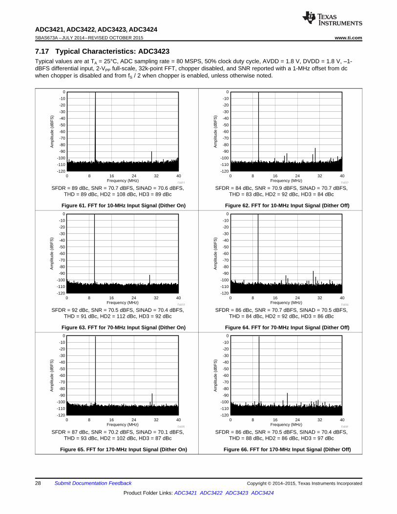
7.17 Typical Characteristics: ADC3423Typical values are at TA = 25°C, ADC sampling rate = 80 MSPS, 50% clock duty cycle, AVDD = 1.8 V, DVDD = 1.8 V, –1-dBFS differential input, 2-VPP full-scale, 32k-point FFT, chopper disabled, and SNR reported with a 1-MHz offset from dcwhen chopper is disabled and from fS / 2 when chopper is enabled, unless otherwise noted.
SFDR = 89 dBc, SNR = 70.7 dBFS, SINAD = 70.6 dBFS, SFDR = 84 dBc, SNR = 70.9 dBFS, SINAD = 70.7 dBFS,THD = 89 dBc, HD2 = 108 dBc, HD3 = 89 dBc THD = 83 dBc, HD2 = 92 dBc, HD3 = 84 dBc
Figure 61. FFT for 10-MHz Input Signal (Dither On) Figure 62. FFT for 10-MHz Input Signal (Dither Off)
SFDR = 92 dBc, SNR = 70.5 dBFS, SINAD = 70.4 dBFS, SFDR = 86 dBc, SNR = 70.7 dBFS, SINAD = 70.5 dBFS,THD = 91 dBc, HD2 = 112 dBc, HD3 = 92 dBc THD = 84 dBc, HD2 = 92 dBc, HD3 = 86 dBc
Figure 63. FFT for 70-MHz Input Signal (Dither On) Figure 64. FFT for 70-MHz Input Signal (Dither Off)
SFDR = 87 dBc, SNR = 70.2 dBFS, SINAD = 70.1 dBFS, SFDR = 86 dBc, SNR = 70.5 dBFS, SINAD = 70.4 dBFS,THD = 93 dBc, HD2 = 102 dBc, HD3 = 87 dBc THD = 88 dBc, HD2 = 86 dBc, HD3 = 97 dBc
Figure 65. FFT for 170-MHz Input Signal (Dither On) Figure 66. FFT for 170-MHz Input Signal (Dither Off)
28 Submit Documentation Feedback Copyright © 2014–2015, Texas Instruments Incorporated
Product Folder Links: ADC3421 ADC3422 ADC3423 ADC3424

Frequency (MHz)
Am
plitu
de (
dBF
S)
0 8 16 24 32 40-120
-110
-100
-90
-80
-70
-60
-50
-40
-30
-20
-10
0
D411Frequency (MHz)
Am
plitu
de (
dBF
S)
0 8 16 24 32 40-120
-110
-100
-90
-80
-70
-60
-50
-40
-30
-20
-10
0
D412
Frequency (MHz)
Am
plitu
de (
dBF
S)
0 8 16 24 32 40-120
-110
-100
-90
-80
-70
-60
-50
-40
-30
-20
-10
0
D409Frequency (MHz)
Am
plitu
de (
dBF
S)
0 8 16 24 32 40-120
-110
-100
-90
-80
-70
-60
-50
-40
-30
-20
-10
0
D410
Frequency (MHz)
Am
plitu
de (
dBF
S)
0 8 16 24 32 40-120
-110
-100
-90
-80
-70
-60
-50
-40
-30
-20
-10
0
D407Frequency (MHz)
Am
plitu
de (
dBF
S)
0 8 16 24 32 40-120
-110
-100
-90
-80
-70
-60
-50
-40
-30
-20
-10
0
D408
ADC3421, ADC3422, ADC3423, ADC3424www.ti.com SBAS673A –JULY 2014–REVISED OCTOBER 2015
Typical Characteristics: ADC3423 (continued)Typical values are at TA = 25°C, ADC sampling rate = 80 MSPS, 50% clock duty cycle, AVDD = 1.8 V, DVDD = 1.8 V, –1-dBFS differential input, 2-VPP full-scale, 32k-point FFT, chopper disabled, and SNR reported with a 1-MHz offset from dcwhen chopper is disabled and from fS / 2 when chopper is enabled, unless otherwise noted.
SFDR = 76 dBc, SNR = 69.2 dBFS, SINAD = 68.3 dBFS, SFDR = 75 dBc, SNR = 69.5 dBFS, SINAD = 68.4 dBFS,THD = 75 dBc, HD2 = 76 dBc, HD3 = 81 dBc THD = 75 dBc, HD2 = 75 dBc, HD3 = 82 dBc
Figure 67. FFT for 270-MHz Input Signal (Dither On) Figure 68. FFT for 270-MHz Input Signal (Dither Off)
SFDR = 68 dBc, SNR = 67.5 dBFS, SINAD = 67.1 dBFS, SFDR = 67 dBc SNR = 67.7 dBFS, SINAD = 67.3 dBFS,THD = 77 dBc, HD2 = 68 dBc, HD3 = 89 dBc THD = 77 dBc, HD2 = 67 dBc, HD3 = 84 dBc
Figure 69. FFT for 450-MHz Input Signal (Dither On) Figure 70. FFT for 450-MHz Input Signal (Dither Off)
fIN1 = 46 MHz, fIN2 = 50 MHz, IMD3 = 98 dBFS, fIN1 = 46 MHz, fIN2 = 50 MHz, IMD3 = 105 dBFS,each tone at –7 dBFS each tone at –36 dBFS
Figure 71. FFT for Two-Tone Input Signal Figure 72. FFT for Two-Tone Input Signal(–7 dBFS at 46 MHz and 50 MHz) (–36 dBFS at 46 MHz and 50 MHz)
Copyright © 2014–2015, Texas Instruments Incorporated Submit Documentation Feedback 29
Product Folder Links: ADC3421 ADC3422 ADC3423 ADC3424

Frequency (MHz)
SF
DR
(dB
c)
0 50 100 150 200 250 300 350 40070
75
80
85
90
95
100
D418
Dither_ENDither_DIS
Frequency (MHz)
SN
R (
dBF
S)
0 50 100 150 200 250 300 350 40067
68
69
70
71
72
D417
Dither_ENDither_DIS
Each Tone Amplitude (dBFS)
Tw
o-T
one
IMD
(dB
FS
)
-35 -31 -27 -23 -19 -15 -11 -7-110
-105
-100
-95
-90
-85
D415Each Tone Amplitude (dBFS)
Tw
o-T
one
IMD
(dB
FS
)
-35 -31 -27 -23 -19 -15 -11 -7-110
-105
-100
-95
-90
-85
-80
D416
Frequency (MHz)
Am
plitu
de (
dBF
S)
0 8 16 24 32 40-120
-110
-100
-90
-80
-70
-60
-50
-40
-30
-20
-10
0
D413 Frequency (MHz)
Am
plitu
de (
dBF
S)
0 8 16 24 32 40-120
-110
-100
-90
-80
-70
-60
-50
-40
-30
-20
-10
0
D414
ADC3421, ADC3422, ADC3423, ADC3424SBAS673A –JULY 2014–REVISED OCTOBER 2015 www.ti.com
Typical Characteristics: ADC3423 (continued)Typical values are at TA = 25°C, ADC sampling rate = 80 MSPS, 50% clock duty cycle, AVDD = 1.8 V, DVDD = 1.8 V, –1-dBFS differential input, 2-VPP full-scale, 32k-point FFT, chopper disabled, and SNR reported with a 1-MHz offset from dcwhen chopper is disabled and from fS / 2 when chopper is enabled, unless otherwise noted.
fIN1 = 185 MHz, fIN2 = 190 MHz, IMD3 = 90 dBFS, fIN1 = 185 MHz, fIN2 = 190 MHz, IMD3 = 105 dBFS,each tone at –7 dBFS each tone at –36 dBFS
Figure 73. FFT FOR Two-Tone Input Signal Figure 74. FFT FOR Two-Tone Input Signal(–7 dBFS at 185 MHz and 190 MHz) (–36 dBFS at 185 MHz and 190 MHz)
Figure 75. Intermodulation Distortion vs Input Amplitude Figure 76. Intermodulation Distortion vs Input Amplitude(46 MHz and 50 MHz) (185 MHz and 190 MHz)
Figure 77. Signal-to-Noise Ratio vs Input Frequency Figure 78. Spurious-Free Dynamic Range vsInput Frequency
30 Submit Documentation Feedback Copyright © 2014–2015, Texas Instruments Incorporated
Product Folder Links: ADC3421 ADC3422 ADC3423 ADC3424

Temperature (°C)
SF
DR
(dB
c)
-40 -15 10 35 60 8585
87
89
91
93
95
D423
AVDD = 1.7 VAVDD = 1.75 VAVDD = 1.8 V
AVDD = 1.85 VAVDD = 1.9 V
Temperature (°C)
SN
R (
dBF
S)
-40 -15 10 35 60 8570
70.2
70.4
70.6
70.8
71
D424
AVDD = 1.7 VAVDD = 1.75 VAVDD = 1.8 V
AVDD = 1.85 VAVDD = 1.9 V
Input Common-Mode Voltage (V)
SN
R (
dBF
S)
SF
DR
(dB
c)
0.85 0.9 0.95 1 1.05 1.166 82
68 84
70 86
72 88
74 90
76 92
D421
SNRSFDR
Input Common-Mode Voltage (V)
SN
R (
dBF
S)
SF
DR
(dB
c)
0.85 0.9 0.95 1 1.05 1.166 80
68 82
70 84
72 86
74 88
76 90
D422
SNRSFDR
Amplitude (dBFS)
SN
R (
dBF
S)
SF
DR
(dB
c,dB
FS
)
-70 -60 -50 -40 -30 -20 -10 069 0
69.5 40
70 80
70.5 120
71 160
71.5 200
72 240
D419
SNR (dBFS)SFDR (dBc)SFDR (dBFS)
Amplitude (dBFS)
SN
R (
dBF
S)
SF
DR
(dB
c,dB
FS
)
-70 -60 -50 -40 -30 -20 -10 068 20
68.5 40
69 60
69.5 80
70 100
70.5 120
71 140
71.5 160
72 180
D421D420
SNR (dBFS)SFDR (dBc)SFDR (dBFS)
ADC3421, ADC3422, ADC3423, ADC3424www.ti.com SBAS673A –JULY 2014–REVISED OCTOBER 2015
Typical Characteristics: ADC3423 (continued)Typical values are at TA = 25°C, ADC sampling rate = 80 MSPS, 50% clock duty cycle, AVDD = 1.8 V, DVDD = 1.8 V, –1-dBFS differential input, 2-VPP full-scale, 32k-point FFT, chopper disabled, and SNR reported with a 1-MHz offset from dcwhen chopper is disabled and from fS / 2 when chopper is enabled, unless otherwise noted.
Figure 79. Performance vs Input Amplitude (30 MHz) Figure 80. Performance vs Input Amplitude (170 MHz)
Figure 81. Performance vs Input Common-Mode Voltage Figure 82. Performance vs Input Common-Mode Voltage(170 MHz)(30 MHz)
Figure 83. Spurious-Free Dynamic Range vs Figure 84. Signal-to-Noise Ratio vsAVDD Supply and Temperature (170 MHz) AVDD Supply and Temperature (170 MHz)
Copyright © 2014–2015, Texas Instruments Incorporated Submit Documentation Feedback 31
Product Folder Links: ADC3421 ADC3422 ADC3423 ADC3424

Input Clock Duty Cycle (%)
SN
R (
dBF
S)
SF
DR
(dB
c)
30 35 40 45 50 55 60 65 7070.3 82
70.5 84
70.7 86
70.9 88
71.1 90
71.3 92
D429
SNRSFDR
Input Clock Duty Cycle (%)
SN
R (
dBF
S)
SF
DR
(dB
c)
30 35 40 45 50 55 60 65 7069.8 82
70 84
70.2 86
70.4 88
70.6 90
70.8 92
D430
SNRSFDR
Differential Clock Amplitude (Vpp)
SN
R (
dBF
S)
SF
DR
(dB
c)
0.2 0.4 0.6 0.8 1 1.2 1.4 1.6 1.8 2 2.266 90
68 93
70 96
72 99
74 102
76 105
D427
SNRSFDR
Differential Clock Amplitude (Vpp)
SN
R (
dBF
S)
SF
DR
(dB
c)
0.2 0.4 0.6 0.8 1 1.2 1.4 1.6 1.8 2 2.264 76
66 80
68 84
70 88
72 92
74 96
D428
SNRSFDR
Temperature (°C)
SF
DR
(dB
c)
-40 -15 10 35 60 8580
84
88
92
96
100
D425
DVDD = 1.7 VDVDD = 1.75 VDVDD = 1.8 V
DVDD = 1.85 VDVDD = 1.9 V
Temperature (°C)
SN
R (
dBF
S)
-40 -15 10 35 60 8569.5
69.9
70.3
70.7
71.1
71.5
D426
DVDD = 1.7 VDVDD = 1.75 VDVDD = 1.8 V
DVDD = 1.85 VDVDD = 1.9 V
ADC3421, ADC3422, ADC3423, ADC3424SBAS673A –JULY 2014–REVISED OCTOBER 2015 www.ti.com
Typical Characteristics: ADC3423 (continued)Typical values are at TA = 25°C, ADC sampling rate = 80 MSPS, 50% clock duty cycle, AVDD = 1.8 V, DVDD = 1.8 V, –1-dBFS differential input, 2-VPP full-scale, 32k-point FFT, chopper disabled, and SNR reported with a 1-MHz offset from dcwhen chopper is disabled and from fS / 2 when chopper is enabled, unless otherwise noted.
Figure 85. Spurious-Free Dynamic Range vs Figure 86. Signal-to-Noise Ratio vsDVDD Supply and Temperature (170 MHz) DVDD Supply and Temperature (170 MHz)
Figure 87. Performance vs Clock Amplitude (40 MHz) Figure 88. Performance vs Clock Amplitude (150 MHz)
Figure 89. Performance vs Clock Duty cycle (30 MHz) Figure 90. Performance vs Clock Duty Cycle (150 MHz)
32 Submit Documentation Feedback Copyright © 2014–2015, Texas Instruments Incorporated
Product Folder Links: ADC3421 ADC3422 ADC3423 ADC3424

Frequency (MHz)
Am
plitu
de (
dBF
S)
0 12.5 25 37.5 50 62.5-120
-110
-100
-90
-80
-70
-60
-50
-40
-30
-20
-10
0
D205Frequency (MHz)
Am
plitu
de (
dBF
S)
0 12.5 25 37.5 50 62.5-120
-110
-100
-90
-80
-70
-60
-50
-40
-30
-20
-10
0
D206
Frequency (MHz)
Am
plitu
de (
dBF
S)
0 12.5 25 37.5 50 62.5-120
-110
-100
-90
-80
-70
-60
-50
-40
-30
-20
-10
0
D203Frequency (MHz)
Am
plitu
de (
dBF
S)
0 12.5 25 37.5 50 62.5-120
-110
-100
-90
-80
-70
-60
-50
-40
-30
-20
-10
0
D204
Frequency (MHz)
Am
plitu
de (
dBF
S)
0 12.5 25 37.5 50 62.5-120
-110
-100
-90
-80
-70
-60
-50
-40
-30
-20
-10
0
D201Frequency (MHz)
Am
plitu
de (
dBF
S)
0 12.5 25 37.5 50 62.5-120
-110
-100
-90
-80
-70
-60
-50
-40
-30
-20
-10
0
D202
ADC3421, ADC3422, ADC3423, ADC3424www.ti.com SBAS673A –JULY 2014–REVISED OCTOBER 2015
7.18 Typical Characteristics: ADC3424Typical values are at TA = 25°C, ADC sampling rate = 125 MSPS, 50% clock duty cycle, AVDD = 1.8 V, DVDD = 1.8 V, –1-dBFS differential input, 2-VPP full-scale, 32k-point FFT, chopper disabled, and SNR reported with a 1-MHz offset from dcwhen chopper is disabled and from fS / 2 when chopper is enabled, unless otherwise noted.
SFDR = 97 dBc, SNR = 70.4 dBFS, SINAD = 70.4 dBFS, SFDR = 91 dBc, SNR = 70.7 dBFS, SINAD = 70.6 dBFS,THD = 98 dBc, HD2 = 95 dBc, HD3 = 97 dBc THD = 86 dBc, HD2 = 92 dBc, HD3 = 91 dBc
Figure 91. FFT for 10-MHz Input Signal Figure 92. FFT for 10-MHz Input Signal(Chopper On, Dither On) (Chopper On, Dither Off)
SFDR = 99 dBc, SNR = 70.3 dBFS, SINAD = 70.3 dBFS, SFDR = 91 dBc, SNR = 70.6 dBFS, SINAD = 70.6 dBFS,THD = 95 dBc, HD2 = 103 dBc, HD3 = 99 dBc THD = 87 dBc, HD2 = 91 dBc, HD3 = 95 dBc
Figure 93. FFT for 70-MHz Input Signal (Dither On) Figure 94. FFT for 70-MHz Input Signal (Dither Off)
SFDR = 86 dBc, SNR = 69.8 dBFS, SINAD = 69.8 dBFS, SFDR = 85 dBc, SNR = 70.3 dBFS, SINAD = 70.2 dBFS,THD = 91 dBc, HD2 = 86 dBc, HD3 = 101 dBc THD = 88 dBc, HD2 = 99 dBc, HD3 = 85 dBc
Figure 95. FFT for 170-MHz Input Signal (Dither On) Figure 96. FFT for 170-MHz Input Signal (Dither Off)
Copyright © 2014–2015, Texas Instruments Incorporated Submit Documentation Feedback 33
Product Folder Links: ADC3421 ADC3422 ADC3423 ADC3424

Frequency (MHz)
Am
plitu
de (
dBF
S)
0 12.5 25 37.5 50 62.5-120
-110
-100
-90
-80
-70
-60
-50
-40
-30
-20
-10
0
D211Frequency (MHz)
Am
plitu
de (
dBF
S)
0 12.5 25 37.5 50 62.5-120
-110
-100
-90
-80
-70
-60
-50
-40
-30
-20
-10
0
D212
Frequency (MHz)
Am
plitu
de (
dBF
S)
0 12.5 25 37.5 50 62.5-120
-110
-100
-90
-80
-70
-60
-50
-40
-30
-20
-10
0
D209Frequency (MHz)
Am
plitu
de (
dBF
S)
0 12.5 25 37.5 50 62.5-120
-110
-100
-90
-80
-70
-60
-50
-40
-30
-20
-10
0
D210
Frequency (MHz)
Am
plitu
de (
dBF
S)
0 12.5 25 37.5 50 62.5-120
-110
-100
-90
-80
-70
-60
-50
-40
-30
-20
-10
0
D207Frequency (MHz)
Am
plitu
de (
dBF
S)
0 12.5 25 37.5 50 62.5-120
-110
-100
-90
-80
-70
-60
-50
-40
-30
-20
-10
0
D208
ADC3421, ADC3422, ADC3423, ADC3424SBAS673A –JULY 2014–REVISED OCTOBER 2015 www.ti.com
Typical Characteristics: ADC3424 (continued)Typical values are at TA = 25°C, ADC sampling rate = 125 MSPS, 50% clock duty cycle, AVDD = 1.8 V, DVDD = 1.8 V, –1-dBFS differential input, 2-VPP full-scale, 32k-point FFT, chopper disabled, and SNR reported with a 1-MHz offset from dcwhen chopper is disabled and from fS / 2 when chopper is enabled, unless otherwise noted.
SFDR = 76 dBc, SNR = 68.94 dBFS, SINAD = 68.4 dBFS, SFDR = 76 dBc, SNR = 69.3 dBFS, SINAD = 68.6 dBFS,THD = 75 dBc, HD2 = 76 dBc, HD3 = 81 dBc THD = 75 dBc, HD2 = 76 dBc, HD3 = 82 dBc
Figure 97. FFT for 270-MHz Input Signal (Dither On) Figure 98. FFT for 270-MHz Input Signal (Dither Off)
SFDR = 71 dBc, SNR = 67.2 dBFS, SINAD = 66.5 dBFS, SFDR = 69 dBc, SNR = 67.8 dBFS, SINAD = 66.8 dBFS,THD = 74 dBc, HD2 = 71 dBc, HD3 = 79 dBc THD = 73 dBc, HD2 = 77 dBc, HD3 = 69 dBc
Figure 99. FFT for 450-MHz Input Signal (Dither On) Figure 100. FFT for 450-MHz Input Signal (Dither Off)
fIN1 = 46 MHz, fIN2 = 50 MHz, IMD3 = 100 dBFS, fIN1 = 46 MHz, fIN2 = 50 MHz, IMD3 = 99 dBFS,each tone at –7 dBFS each tone at –36 dBFS
Figure 101. FFT for Two-Tone Input Signal Figure 102. FFT for Two-Tone Input Signal(–7 dBFS at 46 MHz and 50 MHz) (–36 dBFS at 46 MHz and 50 MHz)
34 Submit Documentation Feedback Copyright © 2014–2015, Texas Instruments Incorporated
Product Folder Links: ADC3421 ADC3422 ADC3423 ADC3424

Frequency (MHz)
SN
R (
dBF
S)
0 50 100 150 200 250 300 350 40067
68
69
70
71
72
D217
Dither_ENDither_DIS
Frequency (MHz)
SF
DR
(dB
c)
0 50 100 150 200 250 300 350 40070
75
80
85
90
95
100
D218
Dither_ENDither_DIS
Each Tone Amplitude (dBFS)
Tw
o-T
one
IMD
(dB
FS
)
-35 -31 -27 -23 -19 -15 -11 -7-110
-105
-100
-95
-90
-85
-80
D215Each Tone Amplitude (dBFS)
Tw
o-T
one
IMD
(dB
FS
)
-35 -31 -27 -23 -19 -15 -11 -7-110
-105
-100
-95
-90
-85
-80
D216
Frequency (MHz)
Am
plitu
de (
dBF
S)
0 12.5 25 37.5 50 62.5-120
-110
-100
-90
-80
-70
-60
-50
-40
-30
-20
-10
0
D213 Frequency (MHz)
Am
plitu
de (
dBF
S)
0 12.5 25 37.5 50 62.5-120
-110
-100
-90
-80
-70
-60
-50
-40
-30
-20
-10
0
D214
ADC3421, ADC3422, ADC3423, ADC3424www.ti.com SBAS673A –JULY 2014–REVISED OCTOBER 2015
Typical Characteristics: ADC3424 (continued)Typical values are at TA = 25°C, ADC sampling rate = 125 MSPS, 50% clock duty cycle, AVDD = 1.8 V, DVDD = 1.8 V, –1-dBFS differential input, 2-VPP full-scale, 32k-point FFT, chopper disabled, and SNR reported with a 1-MHz offset from dcwhen chopper is disabled and from fS / 2 when chopper is enabled, unless otherwise noted.
fIN1 = 185 MHz, fIN2 = 190 MHz, IMD3 = 86 dBFS, fIN1 = 185 MHz, fIN2 = 190 MHz, IMD3 = 102 dBFS,each tone at –7 dBFS each tone at –36 dBFS
Figure 103. FFT for Two-Tone Input Signal Figure 104. FFT for Two-Tone Input Signal(–7 dBFS at 185 MHz and 190 MHz) (–36 dBFS at 185 MHz and 190 MHz)
Figure 105. Intermodulation Distortion vs Input Amplitude Figure 106. Intermodulation Distortion vs Input Amplitude(46 MHz and 50 MHz) (185 MHz and 190 MHz)
Figure 107. Signal-to-Noise Ratio vs Input Frequency Figure 108. Spurious-Free Dynamic Range vsInput Frequency
Copyright © 2014–2015, Texas Instruments Incorporated Submit Documentation Feedback 35
Product Folder Links: ADC3421 ADC3422 ADC3423 ADC3424

Temperature (°C)
SF
DR
(dB
c)
-40 -15 10 35 60 8584
86
88
90
92
94
D223
AVDD = 1.7 VAVDD = 1.75 VAVDD = 1.8 V
AVDD = 1.85 VAVDD = 1.9 V
Temperature (°C)
SF
DR
(dB
c)
-40 -15 10 35 60 8568.5
69.3
70.1
70.9
71.7
72.5
D224
AVDD = 1.7 VAVDD = 1.75 VAVDD = 1.8 V
AVDD = 1.85 VAVDD = 1.9 V
Input Common-Mode Voltage (V)
SN
R (
dBF
S)
SF
DR
(dB
c)
0.85 0.9 0.95 1 1.05 1.166 86
68 88
70 90
72 92
74 94
76 96
D221
SNRSFDR
Input Common-Mode Voltage (V)
SN
R (
dBF
S)
SF
DR
(dB
c)
0.85 0.9 0.95 1 1.05 1.166 78
68 80
70 82
72 84
74 86
76 88
D222
SNRSFDR
Amplitude (dBFS)
SN
R (
dBF
S)
SF
DR
(dB
c,dB
FS
)
-70 -60 -50 -40 -30 -20 -10 069 0
69.5 40
70 80
70.5 120
71 160
71.5 200
72 240
D219
SNR (dBFS)SFDR (dBc)SFDR (dBFS)
Amplitude (dBFS)
SN
R (
dBF
S)
SF
DR
(dB
c,dB
FS
)
-70 -60 -50 -40 -30 -20 -10 068 20
68.5 40
69 60
69.5 80
70 100
70.5 120
71 140
71.5 160
72 180
D220
SNR (dBFS)SFDR (dBc)SFDR (dBFS)
ADC3421, ADC3422, ADC3423, ADC3424SBAS673A –JULY 2014–REVISED OCTOBER 2015 www.ti.com
Typical Characteristics: ADC3424 (continued)Typical values are at TA = 25°C, ADC sampling rate = 125 MSPS, 50% clock duty cycle, AVDD = 1.8 V, DVDD = 1.8 V, –1-dBFS differential input, 2-VPP full-scale, 32k-point FFT, chopper disabled, and SNR reported with a 1-MHz offset from dcwhen chopper is disabled and from fS / 2 when chopper is enabled, unless otherwise noted.
Figure 109. Performance vs Input Amplitude (30 MHz) Figure 110. Performance vs Input Amplitude (170 MHz)
Figure 111. Performance vs Input Common-Mode Voltage Figure 112. Performance vs Input Common-Mode Voltage(30 MHz) (170 MHz)
Figure 113. Spurious-Free Dynamic Range vs Figure 114. Signal-to-Noise Ratio vsAVDD Supply and Temperature (170 MHz) AVDD Supply and Temperature (170 MHz)
36 Submit Documentation Feedback Copyright © 2014–2015, Texas Instruments Incorporated
Product Folder Links: ADC3421 ADC3422 ADC3423 ADC3424

Input Clock Duty Cycle (%)
SN
R (
dBF
S)
SF
DR
(dB
c)
30 35 40 45 50 55 60 65 7069.5 86
69.9 88
70.3 90
70.7 92
71.1 94
71.5 96
D229
SNRSFDR
Input Clock Duty Cycle (%)
SN
R (
dBF
S)
SF
DR
(dB
c)
30 35 40 45 50 55 60 65 7069.5 77.5
69.7 80
69.9 82.5
70.1 85
70.3 87.5
70.5 90
D230
SNRSFDR
Differential Clock Amplitude (Vpp)
SN
R (
dBF
S)
SF
DR
(dB
c)
0.2 0.4 0.6 0.8 1 1.2 1.4 1.6 1.8 2 2.268.5 65
69 70
69.5 75
70 80
70.5 85
71 90
71.5 95
72 100
72.5 105
D227
SNRSFDR
Differential Clock Amplitude (Vpp)
SN
R (
dBF
S)
SF
DR
(dB
c)
0.2 0.4 0.6 0.8 1 1.2 1.4 1.6 1.8 2 2.265 65
66 70
67 75
68 80
69 85
70 90
71 95
72 100
73 105
D228
SNRSFDR
Temperature (°C)
SF
DR
(dB
c)
-40 -15 10 35 60 8584
86
88
90
92
94
D225
DVDD = 1.7 VDVDD = 1.75 VDVDD = 1.8 V
DVDD = 1.85 VDVDD = 1.9 V
Temperature (°C)
SN
R (
dBF
S)
-40 -15 10 35 60 8569.5
69.9
70.3
70.7
71.1
71.5
D226
DVDD = 1.7 VDVDD = 1.75 VDVDD = 1.8 V
DVDD = 1.85 VDVDD = 1.9 V
ADC3421, ADC3422, ADC3423, ADC3424www.ti.com SBAS673A –JULY 2014–REVISED OCTOBER 2015
Typical Characteristics: ADC3424 (continued)Typical values are at TA = 25°C, ADC sampling rate = 125 MSPS, 50% clock duty cycle, AVDD = 1.8 V, DVDD = 1.8 V, –1-dBFS differential input, 2-VPP full-scale, 32k-point FFT, chopper disabled, and SNR reported with a 1-MHz offset from dcwhen chopper is disabled and from fS / 2 when chopper is enabled, unless otherwise noted.
Figure 115. Spurious-Free Dynamic Range vs Figure 116. Signal-to-Noise Ratio vsDVDD Supply and Temperature (170 MHz) DVDD Supply and Temperature (170 MHz)
Figure 117. Performance vs Clock Amplitude (40 MHz) Figure 118. Performance vs Clock Amplitude (150 MHz)
Figure 119. Performance vs Clock Duty Cycle (30 MHz) Figure 120. Performance vs Clock Duty Cycle (150 MHz)
Copyright © 2014–2015, Texas Instruments Incorporated Submit Documentation Feedback 37
Product Folder Links: ADC3421 ADC3422 ADC3423 ADC3424

Sampling Speed (MSPS)
Pow
er C
onsu
mpt
ion
(mW
)
5 15 25 35 45 55 65 75 85 95 105 115 12580
120
160
200
240
280
320
360
400
D009
Analog PowerDigital PowerTotal Power
Sampling Speed (MSPS)
Pow
er C
onsu
mpt
ion
(mW
)
10 20 30 40 50 60 70 8040
80
120
160
200
240
280
320
D010
Analog PowerDigital PowerTotal Power
Frequency (MHz)
Am
pli
tud
e (
dB
FS
)
0 12.5 25 37.5 50 62.5
-120
-110
-100
-90
-80
-70
-60
-50
-40
-30
-20
-10
0
D004Frequency of Input Common-Mode Signal (MHz)
CM
RR
(dB
)
0 50 100 150 200 250 300-70
-65
-60
-55
-50
-45
-40
-35
-30
-25
-20
D003
Frequency (MHz)
Am
pli
tud
e (
dB
FS
)
0 12.5 25 37.5 50 62.5
-120
-110
-100
-90
-80
-70
-60
-50
-40
-30
-20
-10
0
D002Frequency of Signal on Supply (MHz)
PS
RR
(dB
)
0 50 100 150 200 250 300-50
-45
-40
-35
-30
-25
-20
-15
-10
-5
0
D001
ADC3421, ADC3422, ADC3423, ADC3424SBAS673A –JULY 2014–REVISED OCTOBER 2015 www.ti.com
7.19 Typical Characteristics: CommonTypical values are at TA = 25°C, ADC sampling rate = 125 MSPS, 50% clock duty cycle, AVDD = 1.8 V, DVDD = 1.8 V, –1-dBFS differential input, 2-VPP full-scale, 32k-point FFT, chopper disabled, and SNR reported with a 1-MHz offset from dcwhen chopper is disabled and from fS / 2 when chopper is enabled, unless otherwise noted.
fIN = 30 MHz, AIN = –1 dBFS, fIN = 30.1 MHz, fPSRR = 3 MHz, APSRR = 50 mVPP,test signal amplitude = 50 mVPP SINAD = 58.51 dBFS, SFDR = 60 dBc
Figure 121. Power-Supply Rejection Ratio vs Figure 122. Power-Supply Rejection Ratio SpectrumTest Signal Frequency
fIN = 30 MHz, AIN = –1 dBFS, fIN = 170.1 MHz, fCMRR = 5 MHz, ACMRR = 50 mVPP,test signal amplitude = 50 mVPP SINAD = 69.66 dBFS, SFDR = 75 dBc
Figure 123. Common-Mode Rejection Ratio vs Figure 124. Common-Mode Rejection Ratio SpectrumTest Signal Frequency
Figure 125. Power vs Sampling Frequency Figure 126. Power vs Sampling Frequency(Two-Wire Mode) (One-Wire Mode)
38 Submit Documentation Feedback Copyright © 2014–2015, Texas Instruments Incorporated
Product Folder Links: ADC3421 ADC3422 ADC3423 ADC3424

DAn_PDBn_P
DAn_MDBn_M
GND
Logic 0
V(1)
ODL = 350 mV-
Logic 1
V(1)
ODH = +350 mV
VOCM
69
69
69
73
73
73
77
77
77
81
81
81
85
85
85
85
89
89
89
Input Frequency, MHz
Sam
plin
g F
requ
ency
, MS
PS
50 100 150 200 250 300 350 400 450
30
40
50
60
70
80
90
100
110
120
70 75 80 85
66.567
67.5
67.5
67.5
68
68
68
68.5
68.5
68.5
69
69
69
69.5
69.5
69.5
70
70
70
70.5
70.5
70.5
Input Frequency, MHz
Sam
plin
g F
requ
ency
, MS
PS
50 100 150 200 250 300 350 400 450
30
40
50
60
70
80
90
100
110
120
66 66.5 67 67.5 68 68.5 69 69.5 70 70.5
ADC3421, ADC3422, ADC3423, ADC3424www.ti.com SBAS673A –JULY 2014–REVISED OCTOBER 2015
7.20 Typical Characteristics: ContourTypical values are at TA= 25°C, ADC sampling rate = 125 MSPS, 50% clock duty cycle, AVDD = 1.8 V, DVDD = 1.8 V, –1-dBFS differential input, 2-VPP full-scale, 32k-point FFT, chopper disabled, and SNR reported with a 1-MHz offset from dcwhen chopper is disabled and from fS / 2 when is chopper enabled, unless otherwise noted.
Figure 127. Spurious-Free Dynamic Range (SFDR) Figure 128. Signal-to-Noise Ratio (SNR)
8 Parameter Measurement Information
8.1 Timing Diagrams
(1) With an external 100-Ω termination.
Figure 129. Serial LVDS Output Voltage Levels
Copyright © 2014–2015, Texas Instruments Incorporated Submit Documentation Feedback 39
Product Folder Links: ADC3421 ADC3422 ADC3423 ADC3424

DCLK
Dx0P
Dx0M
t HO
t SU
Dx0P
Dx0M
D10
D4
SAMPLE NSAMPLE N-1
D 0
D9
SAMPLE N+1
DCLK
FCLK
D11
D0
D1
D2
D3
D5
D11
D6
D7
D8
D9
D10
CLKIN
1-Wire (12x Serialization)
D5
D5
D 11
D11
D 0
DCLK
D0
D1
D2
D3
D4
D6
D7
D8
D9
D10
D 6
2-Wire (6x Serialization)Dx0P
Dx0M
Dx1P
Dx1M
ADC3421, ADC3422, ADC3423, ADC3424SBAS673A –JULY 2014–REVISED OCTOBER 2015 www.ti.com
Timing Diagrams (continued)
Figure 130. Output Timing Diagram
Figure 131. Setup and Hold Time
40 Submit Documentation Feedback Copyright © 2014–2015, Texas Instruments Incorporated
Product Folder Links: ADC3421 ADC3422 ADC3423 ADC3424

CLKPCLKM
INBPINBM
Configuration Registers
SC
LK
SE
N
SD
AT
A
SD
OU
T
RE
SE
T
CommonMode
VCM
DA1PDA1M
DB1PDB1M
DA0PDA0M
DB0PDB0MDigital Encoder
and Serializer
SYSREFPSYSREFM
Divide by 1,2,4
INAPINAM
12-Bit ADC
Digital Encoder and Serializer
INDPINDM
12-Bit ADC
INCPINCM
12-Bit ADC
PLL
12-Bit ADC
FCLKPFCLKM
DCLKPDCLKM
Bit Clock
Frame Clock
DC1PDC1M
DD1PDD1M
DC0PDC0M
DD0PDD0MDigital Encoder
and Serializer
Digital Encoder and Serializer
ADC3421, ADC3422, ADC3423, ADC3424www.ti.com SBAS673A –JULY 2014–REVISED OCTOBER 2015
9 Detailed Description
9.1 OverviewThe ADC342x are a high-linearity, ultra-low power, quad-channel, 12-bit, 25-MSPS to 125-MSPS, analog-to-digital converter (ADC) family. The devices are designed specifically to support demanding, high input frequencysignals with large dynamic range requirements. An input clock divider allows more flexibility for system clockarchitecture design and the SYSREF input enables complete system synchronization. The ADC342x familysupports a serial low-voltage differential signaling (LVDS) interface in order to reduce the number of interfacelines, thus allowing for high system integration density. The serial LVDS interface is two-wire, where each ADCdata are serialized and output over two LVDS pairs. An internal phase-locked loop (PLL) multiplies the incomingADC sampling clock to derive the bit clock that is used to serialize the 12-bit output data from each channel. Inaddition to the serial data streams, the frame and bit clocks are also transmitted as LVDS outputs.
9.2 Functional Block Diagram
Copyright © 2014–2015, Texas Instruments Incorporated Submit Documentation Feedback 41
Product Folder Links: ADC3421 ADC3422 ADC3423 ADC3424

CLKP
CLKM
0.1 FmZo
Device
100 W
0.1 FmZo
Typical LVPECL
Clock Input
150 W
150 W
CLKP
CLKM
0.1 Fm
100 W
Zo
Device
0.1 FmZo
Typical LVDS
Clock Input
CLKP
CLKM
0.1 Fm
RT
Device
0.1 Fm
Differential
Sine-Wave
Clock Input
ADC3421, ADC3422, ADC3423, ADC3424SBAS673A –JULY 2014–REVISED OCTOBER 2015 www.ti.com
9.3 Feature Description
9.3.1 Analog InputsThe ADC342x analog signal inputs are designed to be driven differentially. Each input pin (INP, INM) must swingsymmetrically between (VCM + 0.5 V) and (VCM – 0.5 V), resulting in a 2-VPP (default) differential input swing.The input sampling circuit has a 3-dB bandwidth that extends up to 540 MHz (50-Ω source driving 50-Ωtermination between INP and INM).
9.3.2 Clock InputThe device clock inputs can be driven differentially (sine, LVPECL, or LVDS) or single-ended (LVCMOS), withlittle or no difference in performance between them. The common-mode voltage of the clock inputs is set to0.95 V using internal 5-kΩ resistors. The self-bias clock inputs of the ADC342x can be driven by the transformer-coupled, sine-wave clock source or by the ac-coupled, LVPECL and LVDS clock sources, as shown inFigure 132, Figure 133, and Figure 134. See Figure 135 for details regarding the internal clock buffer.
NOTE: RT = termination resistor, if necessary.
Figure 132. Differential Sine-Wave Clock Driving Figure 133. LVDS Clock Driving CircuitCircuit
Figure 134. LVPECL Clock Driving Circuit
42 Submit Documentation Feedback Copyright © 2014–2015, Texas Instruments Incorporated
Product Folder Links: ADC3421 ADC3422 ADC3423 ADC3424
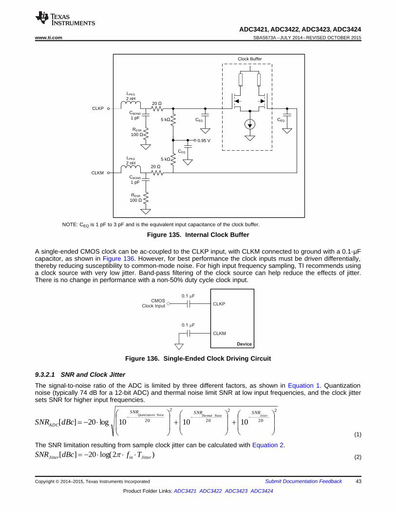
)2log(20][ JitterinJitter TfdBcSNR S
2
20
2
20
2
20 101010log20][¸¸
¹
·
¨¨
©
§
¸¸
¹
·
¨¨
©
§
¸¸
¹
·
¨¨
©
§
JitterNoiseThermalNoiseinQuantizatoSNRSNRSNR
ADC dBcSNR
CLKP
CLKM
0.1 Fm
CMOSClock Input
Device
0.1 Fm
CEQCEQ
CEQ
CBOND
1 pF
CBOND
1 pF
Clock Buffer
RESR
100
LPKG
2 nH
LPKG
2 nH
RESR
100
20
20
CLKP
CLKM
5 k
5 k
0.95 V
ADC3421, ADC3422, ADC3423, ADC3424www.ti.com SBAS673A –JULY 2014–REVISED OCTOBER 2015
NOTE: CEQ is 1 pF to 3 pF and is the equivalent input capacitance of the clock buffer.
Figure 135. Internal Clock Buffer
A single-ended CMOS clock can be ac-coupled to the CLKP input, with CLKM connected to ground with a 0.1-μFcapacitor, as shown in Figure 136. However, for best performance the clock inputs must be driven differentially,thereby reducing susceptibility to common-mode noise. For high input frequency sampling, TI recommends usinga clock source with very low jitter. Band-pass filtering of the clock source can help reduce the effects of jitter.There is no change in performance with a non-50% duty cycle clock input.
Figure 136. Single-Ended Clock Driving Circuit
9.3.2.1 SNR and Clock JitterThe signal-to-noise ratio of the ADC is limited by three different factors, as shown in Equation 1. Quantizationnoise (typically 74 dB for a 12-bit ADC) and thermal noise limit SNR at low input frequencies, and the clock jittersets SNR for higher input frequencies.
(1)
The SNR limitation resulting from sample clock jitter can be calculated with Equation 2.
(2)
Copyright © 2014–2015, Texas Instruments Incorporated Submit Documentation Feedback 43
Product Folder Links: ADC3421 ADC3422 ADC3423 ADC3424

Input Frequency (MHz)
SN
R (
dBF
S)
10 100 100065.0
65.5
66.0
66.5
67.0
67.5
68.0
68.5
69.0
69.5
70.0
70.5
71.0
D001D036
Ext Clock Jitter35 fs50 fs100 fs150 fs200 fs
2_
2_., )()( ADCApertureInputClockExtJitterJitter TTT
ADC3421, ADC3422, ADC3423, ADC3424SBAS673A –JULY 2014–REVISED OCTOBER 2015 www.ti.com
The total clock jitter (TJitter) has two components: the internal aperture jitter (130 fs for the device) which is set bythe noise of the clock input buffer and the external clock. TJitter can be calculated with Equation 3.
(3)
External clock jitter can be minimized by using high-quality clock sources and jitter cleaners as well as band-passfilters at the clock input; a faster clock slew rate improves the ADC aperture jitter. The devices have a typicalthermal noise of 72.7 dBFS and internal aperture jitter of 130 fs. The SNR, depending on the amount of externaljitter for different input frequencies, is shown in Figure 137.
Figure 137. SNR vs Frequency for Different Clock Jitter
9.3.3 Digital Output InterfaceThe devices offer two different output format options, thus making interfacing to a field-programmable gate array(FPGA) or an application-specific integrated circuit (ASIC) easy. Each option can be easily programmed usingthe serial interface, as shown in Table 3. The output interface options are:• One-wire, 1x frame clock, 12x serialization with the DDR bit clock and• Two-wire, 1x frame clock, 6x serialization with the DDR bit clock.
Table 3. Interface RatesRECOMMENDED SAMPLING BIT CLOCK FRAME CLOCK SERIAL DATAINTERFACE FREQUENCY (MSPS)SERIALIZATION FREQUENCY FREQUENCY RATE PEROPTIONS (MHz) (MHz) WIRE (Mbps)MINIMUM MAXIMUM
15 90 15 180One-wire 12x
80 480 80 960Two-wire 20 (1) 60 20 120
(Default after 6x125 375 125 750Reset)
(1) Use the LOW SPEED ENABLE register bits for low speed operation; see Table 21.
9.3.3.1 One-Wire Interface: 12x SerializationIn this interface option, the device outputs the data of each ADC serially on a single LVDS pair (one-wire). Thedata are available at the rising and falling edges of the bit clock (DDR bit clock). The ADC outputs a new word atthe rising edge of every frame clock, starting with the LSB. The data rate is 12x sample frequency (12xserialization).
44 Submit Documentation Feedback Copyright © 2014–2015, Texas Instruments Incorporated
Product Folder Links: ADC3421 ADC3422 ADC3423 ADC3424

Dx0P
Dx0M
D10
D4
SAMPLE NSAMPLE N-1
D 0
D9
SAMPLE N+1
DCLK
FCLK
D11
D0
D1
D2
D3
D5
D11
D6
D7
D8
D9
D10
CLKIN
1-Wire (12x Serialization)
D5
D5
D 11
D11
D 0
DCLK
D0
D1
D2
D3
D4
D6
D7
D8
D9
D10
D 6
2-Wire (6x Serialization)Dx0P
Dx0M
Dx1P
Dx1M
ADC3421, ADC3422, ADC3423, ADC3424www.ti.com SBAS673A –JULY 2014–REVISED OCTOBER 2015
9.3.3.2 Two-Wire Interface: 6x SerializationThe two-wire interface is recommended for sampling frequencies above 65 MSPS. The output data rate is 6xsample frequency because six data bits are output every clock cycle on each differential pair. Each ADC sampleis sent over the two wires with the six MSBs on Dx1P, Dx1M and the six LSBs on Dx0P, Dx0M, as shown inFigure 138.
Figure 138. Output Timing Diagram
Copyright © 2014–2015, Texas Instruments Incorporated Submit Documentation Feedback 45
Product Folder Links: ADC3421 ADC3422 ADC3423 ADC3424

Frequency (MHz)
Atte
nuat
ion
(dB
)
0 10 20 30 40 50 60-120
-100
-80
-60
-40
-20
0
D016Frequency (MHz)
Atte
nuat
ion
(dB
)
0 10 20 30 40 50 60-120
-100
-80
-60
-40
-20
0
D017
ADC3421, ADC3422, ADC3423, ADC3424SBAS673A –JULY 2014–REVISED OCTOBER 2015 www.ti.com
9.4 Device Functional Modes
9.4.1 Input Clock DividerThe devices are equipped with an internal divider on the clock input. The clock divider allows operation with afaster input clock, thus simplifying the system clock distribution design. The clock divider can be bypassed foroperation with a 125-MHz clock and the divide-by-2 option supports a maximum input clock of 250 MHz and thedivide-by-4 option provides a maximum input clock frequency of 500 MHz.
9.4.2 Chopper FunctionalityThe devices are equipped with an internal chopper front-end. Enabling the chopper function swaps the ADCnoise spectrum by shifting the 1/f noise from dc to fS / 2. Figure 139 shows the noise spectrum with the chopperoff and Figure 140 shows the noise spectrum with the chopper on. This function is especially useful inapplications requiring good ac performance at low input frequencies or in dc-coupled applications. The choppercan be enabled via SPI register writes and is recommended for input frequencies below 30 MHz. The chopperfunction creates a spur at fS / 2 that must be filtered out digitally.
fS = 125 MSPS, SNR = 70.4 dBFS, fS = 125 MSPS, SNR = 70.4 dBFS,fIN = 10 MHz, SFDR = 98 dBc fIN = 10 MHz, SFDR = 97 dBc
Figure 139. Chopper Off Figure 140. Chopper On
9.4.3 Power-Down ControlThe power-down functions of the ADC342x can be controlled either through the parallel control pin (PDN) orthrough an SPI register setting (see register 15h). The PDN pin can also be configured via SPI to a global power-down or standby functionality, as shown in Table 4.
Table 4. Power-Down ModesFUNCTION POWER CONSUMPTION (mW) WAKE-UP TIME (µs)
Global power-down 5 85Standby 45 35
46 Submit Documentation Feedback Copyright © 2014–2015, Texas Instruments Incorporated
Product Folder Links: ADC3421 ADC3422 ADC3423 ADC3424

Frequency (MHz)
Am
plitu
de (
dBF
S)
0 12.5 25 37.5 50 62.5-120
-110
-100
-90
-80
-70
-60
-50
-40
-30
-20
-10
0
D201Frequency (MHz)
Am
plitu
de (
dBF
S)
0 12.5 25 37.5 50 62.5-120
-110
-100
-90
-80
-70
-60
-50
-40
-30
-20
-10
0
D202
ADC3421, ADC3422, ADC3423, ADC3424www.ti.com SBAS673A –JULY 2014–REVISED OCTOBER 2015
9.4.4 Internal Dither AlgorithmThe ADC342x use an internal dither algorithm to achieve high SFDR and a clean spectrum. However, the ditheralgorithm marginally degrades SNR, creating a trade-off between SNR and SFDR. If desired, the dither algorithmcan be turned off by using the DIS DITH CHx registers bits. Figure 141 and Figure 142 show the effect of usingdither algorithms.
SFDR = 95 dBc, SNR = 70.4 dBFS, SINAD = 70.4 dBFS, SFDR = 91 dBc, SNR = 70.7 dBFS, SINAD = 70.6 dBFS,THD = 98 dBc, HD2 = 95 dBc, HD3 = 97 dBc THD = 86 dBc, HD2 = 92 dBc, HD3 = 91 dBc
Figure 141. FFT for 10-MHz Input Signal Figure 142. FFT for 10-MHz Input Signal(Chopper On, Dither On) (Chopper On, Dither Off)
9.4.5 Summary of Performance Mode RegistersTable 5 lists the location, value, and functions of performance mode registers in the device.
Table 5. Performance ModesMODE REGISTER SETTINGS DESCRIPTION
Special modes Registers 139 (bit 3), 239 (bit 3), 439 (bit 3), and 539 (bit 3) Always write 1 for best performanceRegisters 1 (bits 7:0), 134 (bits 5 and 3), 234 (bits 5 and 3),Disable dither Disable dither to improve SNR434 (bits 5 and 3), and 534 (bits 5 and 3)
Disable chopper Registers 122 (bit 1), 222 (bit 1), 422 (bit 1), and 522 (bit 1) Disable chopper (shifts 1/f noise floor at dc)Registers 11Dh (bit 1), 21Dh (bit 1), 41Dh (bit 1), 51Dh (bit 1),High IF modes Improves HD3 by a couple of dB for IF > 100 MHz308h (bits 7-6) and 608h (bits 7-6)
9.5 ProgrammingThe ADC342x can be configured using a serial programming interface, as described in this section.
9.5.1 Serial InterfaceThe device has a set of internal registers that can be accessed by the serial interface formed by the SEN (serialinterface enable), SCLK (serial interface clock), SDATA (serial interface data), and SDOUT (serial interface dataoutput) pins. Serially shifting bits into the device is enabled when SEN is low. Serial data SDATA are latched atevery SCLK rising edge when SEN is active (low). The serial data are loaded into the register at every 24thSCLK rising edge when SEN is low. When the word length exceeds a multiple of 24 bits, the excess bits areignored. Data can be loaded in multiples of 24-bit words within a single active SEN pulse. The interface canfunction with SCLK frequencies from 20 MHz down to very low speeds (of a few hertz) and also with a non-50%SCLK duty cycle.
Copyright © 2014–2015, Texas Instruments Incorporated Submit Documentation Feedback 47
Product Folder Links: ADC3421 ADC3422 ADC3423 ADC3424

R/W A13 A12 A11 A1 A0 D7 D6 D5 D4 D3 D2 D1 D0
Register Address [13:0] Register Data [7:0]
SDATA
SCLK
tSCLK tDSU
tDH
SEN
tSLOADS tSLOADH
RESET
1
= 0
ADC3421, ADC3422, ADC3423, ADC3424SBAS673A –JULY 2014–REVISED OCTOBER 2015 www.ti.com
Programming (continued)9.5.1.1 Register InitializationAfter power-up, the internal registers must be initialized to their default values through a hardware reset byapplying a high pulse on the RESET pin (of durations greater than 10 ns), as shown in Figure 143. If required,the serial interface registers can be cleared during operation either:1. Through a hardware reset, or2. By applying a software reset. When using the serial interface, set the RESET bit (D0 in register address 06h)
high. This setting initializes the internal registers to the default values and then self-resets the RESET bit low.In this case, the RESET pin is kept low.
9.5.1.1.1 Serial Register Write
The device internal register can be programmed with these steps:1. Drive the SEN pin low,2. Set the R/W bit to 0 (bit A15 of the 16-bit address),3. Set bit A14 in the address field to 1,4. Initiate a serial interface cycle by specifying the address of the register (A13 to A0) whose content must be
written, and5. Write the 8-bit data that are latched in on the SCLK rising edge.
Figure 143 and Table 6 show the timing requirements for the serial register write operation.
Figure 143. Serial Register Write Timing Diagram
Table 6. Serial Interface Timing (1)
MIN TYP MAX UNITfSCLK SCLK frequency (equal to 1 / tSCLK) > dc 20 MHztSLOADS SEN to SCLK setup time 25 nstSLOADH SCLK to SEN hold time 25 nstDSU SDIO setup time 25 nstDH SDIO hold time 25 ns
(1) Typical values are at 25°C, full temperature range is from TMIN = –40°C to TMAX = 85°C, and AVDD = DVDD = 1.8 V, unless otherwisenoted.
48 Submit Documentation Feedback Copyright © 2014–2015, Texas Instruments Incorporated
Product Folder Links: ADC3421 ADC3422 ADC3423 ADC3424

SDOUT
SCLK
tSD_DELAY
R/W A13 A12 A11 A1 A0 D7 D6 D5 D4 D3 D2 D1 D0
Register Address [13:0] Register Data: 'RQ¶W&DUH
SDATA
SCLK
SEN
1
SDOUT D7 D6 D5 D4 D3 D2 D1 D0
Register Read Data [7:0]
= 1
ADC3421, ADC3422, ADC3423, ADC3424www.ti.com SBAS673A –JULY 2014–REVISED OCTOBER 2015
9.5.1.1.2 Serial Register Readout
The device includes a mode where the contents of the internal registers can be read back using the SDOUT pin.This readback mode may be useful as a diagnostic check to verify the serial interface communication betweenthe external controller and the ADC. The procedure to read the contents of the serial registers is as follows:1. Drive the SEN pin low.2. Set the R/W bit (A15) to 1. This setting disables any further writes to the registers.3. Set bit A14 in the address field to 1.4. Initiate a serial interface cycle specifying the address of the register (A13 to A0) whose content must be read.5. The device outputs the contents (D7 to D0) of the selected register on the SDOUT pin.6. The external controller can latch the contents at the SCLK rising edge.7. To enable register writes, reset the R/W register bit to 0.
When READOUT is disabled, the SDOUT pin is in a high-impedance mode. If serial readout is not used, theSDOUT pin must float. Figure 144 shows a timing diagram of the serial register read operation. Data appear onthe SDOUT pin at the SCLK falling edge with an approximate delay (tSD_DELAY) of 20 ns, as shown in Figure 145.
Figure 144. Serial Register Read Timing Diagram
Figure 145. SDOUT Timing Diagram
Copyright © 2014–2015, Texas Instruments Incorporated Submit Documentation Feedback 49
Product Folder Links: ADC3421 ADC3422 ADC3423 ADC3424

Power Supplies
RESET
SEN
t1
t2 t3
ADC3421, ADC3422, ADC3423, ADC3424SBAS673A –JULY 2014–REVISED OCTOBER 2015 www.ti.com
9.5.2 Register InitializationAfter power-up, the internal registers must be initialized to their default values through a hardware reset byapplying a high pulse on the RESET pin, as shown in Figure 146 and Table 7.
Figure 146. Initialization of Serial Registers after Power-Up
Table 7. Power-Up TimingMIN TYP MAX UNIT
t1 Power-on delay from power-up to active high RESET pulse 1 mst2 Reset pulse duration: active high RESET pulse duration 10 nst3 Register write delay from RESET disable to SEN active 100 ns
If required, the serial interface registers can be cleared during operation either:1. Through hardware reset, or2. By applying a software reset. When using the serial interface, set the RESET bit (D0 in register address 06h)
high. This setting initializes the internal registers to the default values and then self-resets the RESET bit low.In this case, the RESET pin is kept low.
50 Submit Documentation Feedback Copyright © 2014–2015, Texas Instruments Incorporated
Product Folder Links: ADC3421 ADC3422 ADC3423 ADC3424

ADC3421, ADC3422, ADC3423, ADC3424www.ti.com SBAS673A –JULY 2014–REVISED OCTOBER 2015
9.6 Register Maps
Table 8. Register Map SummaryREGISTER REGISTER DATAADDRESS, 7 6 5 4 3 2 1 0A[13:0] (Hex)
Register 01h DIS DITH CHA DIS DITH CHB DIS DITH CHC DIS DITH CHD
Register 03h 0 0 0 0 0 0 0 ODD EVEN
Register 04h 0 0 0 0 0 0 0 FLIP WIRE
Register 05h 0 0 0 0 0 0 0 1W-2W
TESTRegister 06h 0 0 0 0 0 0 RESETPATTERN EN
Register 07h 0 0 0 0 0 0 0 OVR ON LSB
ALIGN TEST DATARegister 09h 0 0 0 0 0 0 PATTERN FORMAT
Register 0Ah CHA TEST PATTERN CHB TEST PATTERN
Register 0Bh CHC TEST PATTERN 0 CHD TEST PATTERN
Register 0Eh CUSTOM PATTERN[11:4]
Register 0Fh CUSTOM PATTERN[3:0] 0 0 0 0
Register 13h 0 0 0 0 0 0 LOW SPEED ENABLE
CONFIG PDNRegister 15h CHA PDN CHB PDN CHC PDN CHD PDN STANDBY GLOBAL PDN 0 PIN
Register 25h LVDS SWING
Register 27h CLK DIV 0 0 0 0 0 0
HIGH IFRegister 11Dh 0 0 0 0 0 0 0MODE0
DIS CHOPRegister 122h 0 0 0 0 0 0 0CHA
Register 134h 0 0 DIS DITH CHA 0 DIS DITH CHA 0 0 0
Register 139h 0 0 0 0 SP1 CHA 0 0 0
HIGH IFRegister 21Dh 0 0 0 0 0 0 0MODE1
DIS CHOPRegister 222h 0 0 0 0 0 0 0CHD
Register 234h 0 0 DIS DITH CHD 0 DIS DITH CHD 0 0 0
Register 239h 0 0 0 0 SP1 CHD 0 0 0
Register 308 HIGH IF MODE <5:4> 0 0 0 0 0 0
HIGH IFRegister 41Dh 0 0 0 0 0 0 0MODE2
DIS CHOPRegister 422h 0 0 0 0 0 0 0CHB
Register 434h 0 0 DIS DITH CHB 0 DIS DITH CHB 0 0 0
Register 439h 0 0 0 0 SP1 CHB 0 0 0
HIGH IFRegister 51Dh 0 0 0 0 0 0 0MODE3
DIS CHOPRegister 522h 0 0 0 0 0 0 0CHC
Register 534h 0 0 DIS DITH CHC 0 DIS DITH CHC 0 0 0
Register 539h 0 0 0 0 SP1 CHC 0 0 0
Register 608h HIGH IF MODE <7:6> 0 0 0 0 0 0
Register 70Ah 0 0 0 0 0 0 0 PDN SYSREF
Copyright © 2014–2015, Texas Instruments Incorporated Submit Documentation Feedback 51
Product Folder Links: ADC3421 ADC3422 ADC3423 ADC3424

ADC3421, ADC3422, ADC3423, ADC3424SBAS673A –JULY 2014–REVISED OCTOBER 2015 www.ti.com
9.6.1 Serial Register Description
9.6.1.1 Register 01h (address = 01h)
Figure 147. Register 01h
7 6 5 4 3 2 1 0DIS DITH CHA DIS DITH CHB DIS DITH CHC DIS DITH CHD
R/W-0h R/W-0h R/W-0h R/W-0hLEGEND: R/W = Read/Write; -n = value after reset
Table 9. Register 01h Field DescriptionsBit Field Type Reset Description7-6 DIS DITH CHA R/W 0h These bits enable or disable the on-chip dither. Control this bit
along with bits 5 and 3 of register 134h.00 = Default11 = Dither is disabled for channel A. In this mode, SNR typicallyimproves by 0.2 dB at 70 MHz.
5-4 DIS DITH CHB R/W 0h These bits enable or disable the on-chip dither. Control this bitalong with bits 5 and 3 of register 434h.00 = Default11 = Dither is disabled for channel B. In this mode, SNR typicallyimproves by 0.2 dB at 70 MHz.
3-2 DIS DITH CHC R/W 0h These bits enable or disable the on-chip dither. Control this bitalong with bits 5 and 3 of register 534h.00 = Default11 = Dither is disabled for channel B. In this mode, SNR typicallyimproves by 0.2 dB at 70 MHz.
1-0 DIS DITH CHD R/W 0h These bits enable or disable the on-chip dither. Control this bitalong with bits 5 and 3 of register 234h.00 = Default11 = Dither is disabled for channel B. In this mode, SNR typicallyimproves by 0.2 dB at 70 MHz.
9.6.1.2 Register 03h (address = 03h)
Figure 148. Register 03h
7 6 5 4 3 2 1 00 0 0 0 0 0 0 ODD EVEN
W-0h W-0h W-0h W-0h W-0h W-0h W-0h R/W-0hLEGEND: R/W = Read/Write; W = Write only; -n = value after reset
Table 10. Register 03h Field DescriptionsBit Field Type Reset Description7-6 0 W 0h Must write 0.0 ODD EVEN R/W 0h This bit selects the bit sequence on the output wires (in 2-wire
mode only).0 = Bits 0, 1, 2, and so forth appear on wire-0; bits 7, 8, 9, andso forth appear on wire-1.1 = Bits 0, 2, 4, and so forth appear on wire-0; bits 1, 3, 5, andso forth appear on wire-1.
52 Submit Documentation Feedback Copyright © 2014–2015, Texas Instruments Incorporated
Product Folder Links: ADC3421 ADC3422 ADC3423 ADC3424

ADC3421, ADC3422, ADC3423, ADC3424www.ti.com SBAS673A –JULY 2014–REVISED OCTOBER 2015
9.6.1.3 Register 04h (address = 04h)
Figure 149. Register 04h
7 6 5 4 3 2 1 00 0 0 0 0 0 0 FLIP WIRE
W-0h W-0h W-0h W-0h W-0h W-0h W-0h R/W-0hLEGEND: R/W = Read/Write; W = Write only; -n = value after reset
Table 11. Register 04h Field DescriptionsBit Field Type Reset Description7-1 0 W 0h Must write 0.0 FLIP WIRE R/W 0h This bit flips the data on the output wires. Valid only in two wire
configuration.0 = Default1 = Data on output wires is flipped. Pin D0x becomes D1x, andvice versa.
9.6.1.4 Register 05h (address = 05h)
Figure 150. Register 05h
7 6 5 4 3 2 1 00 0 0 0 0 0 0 1W-2W
W-0h W-0h W-0h W-0h W-0h W-0h W-0h R/W-0hLEGEND: R/W = Read/Write; W = Write only; -n = value after reset
Table 12. Register 05h Field DescriptionsBit Field Type Reset Description7-1 0 W 0h Must write 0.0 1W-2W R/W 0h This bit transmits output data on either one or two wires.
0 = Output data are transmitted on two wires (Dx0P, Dx0M andDx1P, Dx1M)1 = Output data are transmitted on one wire (Dx0P, Dx0M). Inthis mode, the recommended fS is less than 80 MSPS.
9.6.1.5 Register 06h (address = 06h)
Figure 151. Register 06h
7 6 5 4 3 2 1 00 0 0 0 0 0 TEST PATTERN EN RESET
W-0h W-0h W-0h W-0h W-0h W-0h R/W-0h R/W-0hLEGEND: R/W = Read/Write; W = Write only; -n = value after reset
Table 13. Register 06h Field DescriptionsBit Field Type Reset Description7-2 0 W 0h Must write 0.1 TEST PATTERN EN R/W 0h This bit enables test pattern selection for the digital outputs.
0 = Normal output1 = Test pattern output enabled
0 RESET R/W 0h This bit applies a software reset.This bit resets all internal registers to the default values and self-clears to 0.
Copyright © 2014–2015, Texas Instruments Incorporated Submit Documentation Feedback 53
Product Folder Links: ADC3421 ADC3422 ADC3423 ADC3424

ADC3421, ADC3422, ADC3423, ADC3424SBAS673A –JULY 2014–REVISED OCTOBER 2015 www.ti.com
9.6.1.6 Register 07h (address = 07h)
Figure 152. Register 07h
7 6 5 4 3 2 1 00 0 0 0 0 0 0 OVR ON LSB
W-0h W-0h W-0h W-0h W-0h W-0h W-0h R/W-0hLEGEND: R/W = Read/Write; W = Write only; -n = value after reset
Table 14. Register 07h Field DescriptionsBit Field Type Reset Description7-1 0 W 0h Must write 0.0 OVR ON LSB R/W 0h This bit provides OVR information on the LSB bits.
0 = Output data bit 0 functions as the LSB of the 12-bit data1 = Output data bit 0 carries the overrange (OVR) information
9.6.1.7 Register 09h (address = 09h)
Figure 153. Register 09h
7 6 5 4 3 2 1 00 0 0 0 0 0 ALIGN TEST PATTERN DATA FORMAT
W-0h W-0h W-0h W-0h W-0h W-0h R/W-0h R/W-0hLEGEND: R/W = Read/Write; W = Write only; -n = value after reset
Table 15. Register 09h Field DescriptionsBit Field Type Reset Description7-2 0 W 0h Must write 0.1 ALIGN TEST PATTERN R/W 0h This bit aligns the test patterns across the outputs of both
channels.0 = Test patterns of both channels are free running1 = Test patterns of both channels are aligned
0 DATA FORMAT R/W 0h This bit selects th digital output data format.0 = Twos complement1 = Offset binary
54 Submit Documentation Feedback Copyright © 2014–2015, Texas Instruments Incorporated
Product Folder Links: ADC3421 ADC3422 ADC3423 ADC3424

ADC3421, ADC3422, ADC3423, ADC3424www.ti.com SBAS673A –JULY 2014–REVISED OCTOBER 2015
9.6.1.8 Register 0Ah (address = 0Ah)
Figure 154. Register 0Ah
7 6 5 4 3 2 1 0CHA TEST PATTERN CHB TEST PATTERN
R/W-0h R/W-0hLEGEND: R/W = Read/Write; -n = value after reset
Table 16. Register 0Ah Field DescriptionsBit Field Type Reset Description7-4 CHA TEST PATTERN R/W 0h These bits control the test pattern for channel A after the TEST
PATTERN EN bit is set.0000 = Normal operation0001 = All 0's0010 = All 1's0011 = Toggle pattern: data alternate between 101010101010and 0101010101010100 = Digital ramp: data increment by 1 LSB every clock cyclefrom code 0 to 40950101 = Custom pattern: output data are the same asprogrammed by the CUSTOM PATTERN register bits0110 = Deskew pattern: data are AAAh1000 = PRBS pattern: data are a sequence of pseudo randomnumbers1001 = 8-point sine-wave: data are a repetitive sequence of thefollowing eight numbers that form a sine-wave: 0, 599, 2048,3496, 4095, 3496, 2048, and 599Others = Do not use
3-0 CHB TEST PATTERN R/W 0h These bits control the test pattern for channel B after the TESTPATTERN EN bit is set.0000 = Normal operation0001 = All 0's0010 = All 1's0011 = Toggle pattern: data alternate between 101010101010and 0101010101010100 = Digital ramp: data increment by 1 LSB every clock cyclefrom code 0 to 40950101 = Custom pattern: output data are the same asprogrammed by the CUSTOM PATTERN register bits0110 = Deskew pattern: data are AAAh1000 = PRBS pattern: data are a sequence of pseudo randomnumbers1001 = 8-point sine-wave: data are a repetitive sequence of thefollowing eight numbers that form a sine-wave: 0, 599, 2048,3496, 4095, 3496, 2048, and 599Others = Do not use
Copyright © 2014–2015, Texas Instruments Incorporated Submit Documentation Feedback 55
Product Folder Links: ADC3421 ADC3422 ADC3423 ADC3424

ADC3421, ADC3422, ADC3423, ADC3424SBAS673A –JULY 2014–REVISED OCTOBER 2015 www.ti.com
9.6.1.9 Register 0Bh (address = 0Bh)
Figure 155. Register 0Bh
7 6 5 4 3 2 1 0CHC TEST PATTERN CHD TEST PATTERN
R/W-0h R/W-0hLEGEND: R/W = Read/Write; -n = value after reset
Table 17. Register 0Bh Field DescriptionsBit Field Type Reset Description7-4 CHC TEST PATTERN R/W 0h These bits control the test pattern for channel C after the TEST
PATTERN EN bit is set.0000 = Normal operation0001 = All 0's0010 = All 1's0011 = Toggle pattern: data alternate between 101010101010and 010101010101.0100 = Digital ramp: data increment by 1 LSB every clock cyclefrom code 0 to 4095.0110 = Custom pattern: output data are the same asprogrammed by the CUSTOM PATTERN register bits.1000 = Deskew pattern: data are AAAh.1010 = PRBS pattern: data are a sequence of pseudo randomnumbers.1011 = 8-point sine wave: data are a repetitive sequence of thefollowing eight numbers that form a sine-wave: 0, 599, 2048,3496, 4095, 3496, 2048, 599.Others = Do not use
3-0 CHD TEST PATTERN R/W 0h These bits control the test pattern for channel D after the TESTPATTERN EN bit is set.0000 = Normal operation0001 = All 0's0010 = All 1's0011 = Toggle pattern: data alternate between 101010101010and 010101010101.0100 = Digital ramp: data increment by 1 LSB every clock cyclefrom code 0 to 4095.0110 = Custom pattern: output data are the same asprogrammed by the CUSTOM PATTERN register bits.1000 = Deskew pattern: data are AAAh.1010 = PRBS pattern: data are a sequence of pseudo randomnumbers.1011 = 8-point sine wave: data are a repetitive sequence of thefollowing eight numbers that form a sine-wave: 0, 599, 2048,3496, 4095, 3496, 2048, 599.Others = Do not use
9.6.1.10 Register 0Eh (address = 0Eh)
Figure 156. Register 0Eh
7 6 5 4 3 2 1 0CUSTOM PATTERN[11:4]
R/W-0hLEGEND: R/W = Read/Write; -n = value after reset
Table 18. Register 0Eh Field DescriptionsBit Field Type Reset Description7-0 CUSTOM PATTERN[11:4] R/W 0h These bits set the 12-bit custom pattern (bits 11-4) for all
channels.
56 Submit Documentation Feedback Copyright © 2014–2015, Texas Instruments Incorporated
Product Folder Links: ADC3421 ADC3422 ADC3423 ADC3424

ADC3421, ADC3422, ADC3423, ADC3424www.ti.com SBAS673A –JULY 2014–REVISED OCTOBER 2015
9.6.1.11 Register 0Fh (address = 0Fh)
Figure 157. Register 0Fh
7 6 5 4 3 2 1 0CUSTOM PATTERN[3:0] 0 0 0 0
R/W-0h W-0h W-0h W-0h W-0hLEGEND: R/W = Read/Write; W = Write only; -n = value after reset
Table 19. Register 0Fh Field DescriptionsBit Field Type Reset Description7-4 CUSTOM PATTERN[3:0] R/W 0h These bits set the 12-bit custom pattern (bits 3-0) for all
channels.3-0 0 W 0h Must write 0.
9.6.1.12 Register 13h (address = 13h)
Figure 158. Register 13h
7 6 5 4 3 2 1 00 0 0 0 0 0 LOW SPEED ENABLE
W-0h R/W-0h R/W-0h W-0h R/W-0h R/W-0h W-0h R/W-0hLEGEND: R/W = Read/Write; W = Write only; -n = value after reset
Table 20. Register 13h Field DescriptionsBit Field Type Reset Description7-2 0 W 0h Must write 0.1-0 LOW SPEED ENABLE R/W 0h Enables low speed operation in 1-wire and 2-wire mode.
Depending upon sampling frequency, write this bit as perTable 21.
Table 21. LOW SPEED ENABLE Register Settings Across fS
fS, MSPS REGISTER BIT LOW SPEED ENABLEMIN MAX 1-WIRE MODE 2-WIRE MODE25 125 00 0020 25 10 1115 20 10 Not supported
Copyright © 2014–2015, Texas Instruments Incorporated Submit Documentation Feedback 57
Product Folder Links: ADC3421 ADC3422 ADC3423 ADC3424

ADC3421, ADC3422, ADC3423, ADC3424SBAS673A –JULY 2014–REVISED OCTOBER 2015 www.ti.com
9.6.1.13 Register 15h (address = 15h)
Figure 159. Register 15h
7 6 5 4 3 2 1 0CONFIG PDNCHA PDN CHB PDN CHC PDN CHD PDN STANDBY GLOBAL PDN 0 PIN
W-0h R/W-0h R/W-0h W-0h R/W-0h R/W-0h W-0h R/W-0hLEGEND: R/W = Read/Write; W = Write only; -n = value after reset
Table 22. Register 15h Field DescriptionsBit Field Type Reset Description7 CHA PDN W 0h 0 = Normal operation
1 = Power-down channel A6 CHB PDN R/W 0h 0 = Normal operation
1 = Power-down channel B5 CHC PDN R/W 0h 0 = Normal operation
1 = Power-down channel C4 CHD PDN W 0h 0 = Normal operation
1 = Power-down channel D3 STANDBY R/W 0h The ADCs of both channels enter standby.
0 = Normal operation1 = Standby
2 GLOBAL PDN R/W 0h 0 = Normal operation1 = Global power-down
1 0 W 0h Must write 0.0 CONFIG PDN PIN R/W 0h This bit configures the PDN pin as either a global power-down or
standby pin.0 = Logic high voltage on the PDN pin sends the device intoglobal power-down1 = Logic high voltage on the PDN pin sends the device intostandby
9.6.1.14 Register 25h (address = 25h)
Figure 160. Register 25h
7 6 5 4 3 2 1 0LVDS SWING
R/W-0hLEGEND: R/W = Read/Write; -n = value after reset
Table 23. Register 25h Field DescriptionsBit Field Type Reset Description7-0 LVDS SWING R/W 0h These bits control the swing of the LVDS outputs (including the
data output, bit clock, and frame clock).
58 Submit Documentation Feedback Copyright © 2014–2015, Texas Instruments Incorporated
Product Folder Links: ADC3421 ADC3422 ADC3423 ADC3424

ADC3421, ADC3422, ADC3423, ADC3424www.ti.com SBAS673A –JULY 2014–REVISED OCTOBER 2015
9.6.1.15 Register 27h (address = 27h)
Figure 161. Register 27h
7 6 5 4 3 2 1 0CLK DIV 0 0 0 0 0 0R/W-0h W-0h W-0h W-0h W-0h W-0h W-0h
LEGEND: R/W = Read/Write; W = Write only; -n = value after reset
Table 24. Register 27h Field DescriptionsBit Field Type Reset Description7-6 CLK DIV R/W 0h These bits select the internal clock divider for the input sampling
clock.00 = Divide-by-101 = Divide-by-110 = Divide-by-211 = Divide-by-4
5-0 0 W 0h Must write 0.
9.6.1.16 Register 11Dh (address = 11Dh)
Figure 162. Register 11Dh
7 6 5 4 3 2 1 00 0 0 0 0 0 HIGH IF MODE0 0
W-0h W-0h W-0h W-0h W-0h W-0h R/W-0h W-0hLEGEND: R/W = Read/Write; W = Write only; -n = value after reset
Table 25. Register 11Dh Field DescriptionsBit Field Type Reset Description7-2 0 W 0h Must write 0.1 HIGH IF MODE0 Set the HIGH IF MODE[7:0] bits together to 1111.
Improves HD3 by a couple of dB for IF > 100 MHz.0 0 W 0h Must write 0.
9.6.1.17 Register 122h (address = 122h)
Figure 163. Register 122h
7 6 5 4 3 2 1 00 0 0 0 0 0 DIS CHOP CHA 0
W-0h W-0h W-0h W-0h W-0h W-0h R/W-0h W-0hLEGEND: R/W = Read/Write; W = Write only; -n = value after reset
Table 26. Register 122h Field DescriptionsBit Field Type Reset Description7-2 0 W 0h Must write 0.1 DIS CHOP CHA R/W 0h This bit disables the chopper.
Set this bit to shift the 1/f noise floor at dc.0 = 1/f noise floor is centered at fS / 2 (default)1 = Chopper mechanism is disabled; 1/f noise floor is centeredat dc
0 0 W 0h Must write 0.
Copyright © 2014–2015, Texas Instruments Incorporated Submit Documentation Feedback 59
Product Folder Links: ADC3421 ADC3422 ADC3423 ADC3424

ADC3421, ADC3422, ADC3423, ADC3424SBAS673A –JULY 2014–REVISED OCTOBER 2015 www.ti.com
9.6.1.18 Register 134h (address = 134h)
Figure 164. Register 134h
7 6 5 4 3 2 1 00 0 DIS DITH CHA 0 DIS DITH CHA 0 0 0
W-0h W-0h R/W-0h W-0h R/W-0h W-0h W-0h W-0hLEGEND: R/W = Read/Write; W = Write only; -n = value after reset
Table 27. Register 134h Field DescriptionsBit Field Type Reset Description7-6 0 W 0h Must write 0.5 DIS DITH CHA R/W 0h Set this bit along with bits 7 and 6 of register 01h.
00 = Default11 = Dither is disabled for channel A. In this mode, SNR typicallyimproves by 0.2 dB at 70 MHz.
4 0 W 0h Must write 0.3 DIS DITH CHA R/W 0h Set this bit along with bits 7 and 6 of register 01h.
00 = Default11 = Dither is disabled for channel A. In this mode, SNR typicallyimproves by 0.2 dB at 70 MHz.
2-0 0 W 0h Must write 0.
9.6.1.19 Register 139h (address = 139h)
Figure 165. Register 139h
7 6 5 4 3 2 1 00 0 0 0 SP1 CHA 0 0 0
W-0h W-0h W-0h W-0h R/W-0h W-0h W-0h W-0hLEGEND: R/W = Read/Write; W = Write only; -n = value after reset
Table 28. Register 139h Field DescriptionsBit Field Type Reset Description7-4 0 W 0h Must write 0.3 SP1 CHA R/W 0h This bit sets the special mode for best performance on channel
A.Always write 1 after reset.
2-0 0 W 0h Must write 0.
9.6.1.20 Register 21Dh (address = 21Dh)
Figure 166. Register 21Dh
7 6 5 4 3 2 1 00 0 0 0 0 0 HIGH IF MODE1 0
W-0h W-0h W-0h W-0h W-0h W-0h R/W-0h W-0hLEGEND: R/W = Read/Write; W = Write only; -n = value after reset
Table 29. Register 21Dh Field DescriptionsBit Field Type Reset Description7-2 0 W 0h Must write 0.1 HIGH IF MODE1 R/W 0h Set the HIGH IF MODE[7:0] bits together to 1111.
Improves HD3 by a couple of dB for IF > 100 MHz.0 0 W 0h Must write 0.
60 Submit Documentation Feedback Copyright © 2014–2015, Texas Instruments Incorporated
Product Folder Links: ADC3421 ADC3422 ADC3423 ADC3424

ADC3421, ADC3422, ADC3423, ADC3424www.ti.com SBAS673A –JULY 2014–REVISED OCTOBER 2015
9.6.1.21 Register 222h (address = 222h)
Figure 167. Register 222h
7 6 5 4 3 2 1 00 0 0 0 0 0 DIS CHOP CHD 0
W-0h W-0h W-0h W-0h W-0h W-0h R/W-0h W-0hLEGEND: R/W = Read/Write; W = Write only; -n = value after reset
Table 30. Register 222h Field DescriptionsBit Field Type Reset Description7-2 0 W 0h Must write 0.1 DIS CHOP CHD R/W 0h This bit disables the chopper.
Set this bit to shift the 1/f noise floor at dc.0 = 1/f noise floor is centered at fS / 2 (default)1 = Chopper mechanism is disabled; 1/f noise floor is centeredat dc
0 0 W 0h Must write 0.
9.6.1.22 Register 234h (address = 234h)
Figure 168. Register 234h
7 6 5 4 3 2 1 00 0 DIS DITH CHD 0 DIS DITH CHD 0 0 0
W-0h W-0h R/W-0h W-0h R/W-0h W-0h W-0h W-0hLEGEND: R/W = Read/Write; W = Write only; -n = value after reset
Table 31. Register 234h Field DescriptionsBit Field Type Reset Description7-6 0 W 0h Must write 0.5 DIS DITH CHD R/W 0h Set this bit with bits 1 and 0 of register 01h.
00 = Default11 = Dither is disabled for channel D. In this mode, SNRtypically improves by 0.2 dB at 70 MHz.
4 0 W 0h Must write 0.3 DIS DITH CHD R/W 0h Set this bit with bits 1 and 0 of register 01h.
00 = Default11 = Dither is disabled for channel D. In this mode, SNRtypically improves by 0.2 dB at 70 MHz.
2-0 0 W 0h Must write 0.
Copyright © 2014–2015, Texas Instruments Incorporated Submit Documentation Feedback 61
Product Folder Links: ADC3421 ADC3422 ADC3423 ADC3424

ADC3421, ADC3422, ADC3423, ADC3424SBAS673A –JULY 2014–REVISED OCTOBER 2015 www.ti.com
9.6.1.23 Register 239h (address = 239h)
Figure 169. Register 239h
7 6 5 4 3 2 1 00 0 0 0 SP1 CHD 0 0 0
W-0h W-0h W-0h W-0h R/W-0h W-0h W-0h W-0hLEGEND: R/W = Read/Write; W = Write only; -n = value after reset
Table 32. Register 239h Field DescriptionsBit Field Type Reset Description7-4 0 W 0h Must write 0.3 SP1 CHD R/W 0h This bit sets the special mode for best performance on channel
D.Always write 1 after reset.
2-0 0 W 0h Must write 0.
9.6.1.24 Register 308h (address = 308h)
Figure 170. Register 308h
7 6 5 4 3 2 1 0HIGH IF MODE<5:4> 0 0 0 0 0 0W-0h W-0h W-0h W-0h W-0h W-0h R/W-0h W-0h
LEGEND: R/W = Read/Write; W = Write only; -n = value after reset
Table 33. Register 308h Field DescriptionsBit Field Type Reset Description7-6 HIGH IF MODE<5:4> R/W 0h Set the HIGH IF MODE[7:0] bits together to FFh.
Improves HD3 by a couple of dB for IF > 100 MHz.5-0 0 W 0h Must write 0.
9.6.1.25 Register 41Dh (address = 41Dh)
Figure 171. Register 41Dh
7 6 5 4 3 2 1 00 0 0 0 0 0 HIGH IF MODE2 0
W-0h W-0h W-0h W-0h W-0h W-0h R/W-0h W-0hLEGEND: R/W = Read/Write; W = Write only; -n = value after reset
Table 34. Register 41Dh Field DescriptionsBit Field Type Reset Description7-2 0 W 0h Must write 0.1 HIGH IF MODE2 R/W 0h Set the HIGH IF MODE[7:0] bits together to FFh.
Improves HD3 by a couple of dB for IF > 100 MHz.0 0 W 0h Must write 0.
62 Submit Documentation Feedback Copyright © 2014–2015, Texas Instruments Incorporated
Product Folder Links: ADC3421 ADC3422 ADC3423 ADC3424

ADC3421, ADC3422, ADC3423, ADC3424www.ti.com SBAS673A –JULY 2014–REVISED OCTOBER 2015
9.6.1.26 Register 422h (address = 422h)
Figure 172. Register 422h
7 6 5 4 3 2 1 00 0 0 0 0 0 DIS CHOP CHB 0
W-0h W-0h W-0h W-0h W-0h W-0h R/W-0h W-0hLEGEND: R/W = Read/Write; W = Write only; -n = value after reset
Table 35. Register 422h Field DescriptionsBit Field Type Reset Description7-2 0 W 0h Must write 0.1 DIS CHOP CHB R/W 0h This bit disables the chopper.
Set this bit to shift the 1/f noise floor at dc.0 = 1/f noise floor is centered at fS / 2 (default)1 = Chopper mechanism is disabled; 1/f noise floor is centeredat dc
0 0 W 0h Must write 0.
9.6.1.27 Register 434h (address = 434h)
Figure 173. Register 434h
7 6 5 4 3 2 1 00 0 DIS DITH CHB 0 DIS DITH CHB 0 0 0
W-0h W-0h R/W-0h W-0h R/W-0h W-0h W-0h W-0hLEGEND: R/W = Read/Write; W = Write only; -n = value after reset
Table 36. Register 434h Field DescriptionsBit Field Type Reset Description7-6 0 W 0h Must write 0.5 DIS DITH CHB R/W 0h Set this bit with bits 5 and 4 of register 01h.
00 = Default11 = Dither is disabled for channel B. In this mode, SNR typicallyimproves by 0.2 dB at 70 MHz.
4 0 W 0h Must write 0.3 DIS DITH CHB R/W 0h Set this bit with bits 5 and 4 of register 01h.
00 = Default11 = Dither is disabled for channel B. In this mode, SNR typicallyimproves by 0.2 dB at 70 MHz.
2-0 0 W 0h Must write 0.
Copyright © 2014–2015, Texas Instruments Incorporated Submit Documentation Feedback 63
Product Folder Links: ADC3421 ADC3422 ADC3423 ADC3424
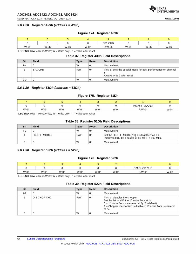
ADC3421, ADC3422, ADC3423, ADC3424SBAS673A –JULY 2014–REVISED OCTOBER 2015 www.ti.com
9.6.1.28 Register 439h (address = 439h)
Figure 174. Register 439h
7 6 5 4 3 2 1 00 0 0 0 SP1 CHB 0 0 0
W-0h W-0h W-0h W-0h R/W-0h W-0h W-0h W-0hLEGEND: R/W = Read/Write; W = Write only; -n = value after reset
Table 37. Register 439h Field DescriptionsBit Field Type Reset Description7-4 0 W 0h Must write 0.3 SP1 CHB R/W 0h This bit sets the special mode for best performance on channel
B.Always write 1 after reset.
2-0 0 W 0h Must write 0.
9.6.1.29 Register 51Dh (address = 51Dh)
Figure 175. Register 51Dh
7 6 5 4 3 2 1 00 0 0 0 0 0 HIGH IF MODE3 0
W-0h W-0h W-0h W-0h W-0h W-0h R/W-0h W-0hLEGEND: R/W = Read/Write; W = Write only; -n = value after reset
Table 38. Register 51Dh Field DescriptionsBit Field Type Reset Description7-2 0 W 0h Must write 0.1 HIGH IF MODE3 R/W 0h Set the HIGH IF MODE[7:0] bits together to FFh.
Improves HD3 by a couple of dB for IF > 100 MHz.0 0 W 0h Must write 0.
9.6.1.30 Register 522h (address = 522h)
Figure 176. Register 522h
7 6 5 4 3 2 1 00 0 0 0 0 0 DIS CHOP CHC 0
W-0h W-0h W-0h W-0h W-0h W-0h R/W-0h W-0hLEGEND: R/W = Read/Write; W = Write only; -n = value after reset
Table 39. Register 522h Field DescriptionsBit Field Type Reset Description7-2 0 W 0h Must write 0.1 DIS CHOP CHC R/W 0h This bit disables the chopper.
Set this bit to shift the 1/f noise floor at dc.0 = 1/f noise floor is centered at fS / 2 (default)1 = Chopper mechanism is disabled; 1/f noise floor is centeredat dc
0 0 W 0h Must write 0.
64 Submit Documentation Feedback Copyright © 2014–2015, Texas Instruments Incorporated
Product Folder Links: ADC3421 ADC3422 ADC3423 ADC3424

ADC3421, ADC3422, ADC3423, ADC3424www.ti.com SBAS673A –JULY 2014–REVISED OCTOBER 2015
9.6.1.31 Register 534h (address = 534h)
Figure 177. Register 534h
7 6 5 4 3 2 1 00 0 DIS DITH CHC 0 DIS DITH CHC 0 0 0
W-0h W-0h R/W-0h W-0h R/W-0h W-0h W-0h W-0hLEGEND: R/W = Read/Write; W = Write only; -n = value after reset
Table 40. Register 534h Field DescriptionsBit Field Type Reset Description7-6 0 W 0h Must write 0.5 DIS DITH CHC R/W 0h Set this bit with bits 3 and 2 of register 01h.
00 = Default11 = Dither is disabled for channel C. In this mode, SNRtypically improves by 0.2 dB at 70 MHz.
4 0 W 0h Must write 0.3 DIS DITH CHC R/W 0h Set this bit with bits 3 and 2 of register 01h.
00 = Default11 = Dither is disabled for channel C. In this mode, SNRtypically improves by 0.2 dB at 70 MHz.
2-0 0 W 0h Must write 0.
9.6.1.32 Register 539h (address = 539h)
Figure 178. Register 539h
7 6 5 4 3 2 1 00 0 0 0 SP1 CHC 0 0 0
W-0h W-0h W-0h W-0h R/W-0h W-0h W-0h W-0hLEGEND: R/W = Read/Write; W = Write only; -n = value after reset
Table 41. Register 539h Field DescriptionsBit Field Type Reset Description7-4 0 W 0h Must write 0.3 SP1 CHC R/W 0h This bit sets the special mode for best performance on channel
C.Always write 1 after reset.
2-0 0 W 0h Must write 0.
9.6.1.33 Register 608h (address = 608h)
Figure 179. Register 608h
7 6 5 4 3 2 1 0HIGH IF MODE<7:6> 0 0 0 0 0 0W-0h W-0h W-0h W-0h W-0h W-0h R/W-0h W-0h
LEGEND: R/W = Read/Write; W = Write only; -n = value after reset
Table 42. Register 608h Field DescriptionsBit Field Type Reset Description7-6 HIGH IF MODE<7:6> R/W 0h Set the HIGH IF MODE[7:0] bits together to FFh.
Improves HD3 by a couple of dB for IF > 100 MHz.5-0 0 W 0h Must write 0.
Copyright © 2014–2015, Texas Instruments Incorporated Submit Documentation Feedback 65
Product Folder Links: ADC3421 ADC3422 ADC3423 ADC3424

Frequency (MHz)
Diff
eren
tial R
esis
tanc
e, R
in (
kOhm
)
0 100 200 300 400 500 600 700 800 900 10000.01
0.1
1
10
D024Frequency (MHz)
Diff
eren
tial C
apac
itanc
e, C
in (
pF)
0 100 200 300 400 500 600 700 800 900 10001
2
3
4
5
6
D001D025
ADC3421, ADC3422, ADC3423, ADC3424SBAS673A –JULY 2014–REVISED OCTOBER 2015 www.ti.com
9.6.1.34 Register 70Ah (address = 70Ah)
Figure 180. Register 70Ah
7 6 5 4 3 2 1 00 0 0 0 0 0 0 PDN SYSREF
W-0h W-0h W-0h W-0h W-0h W-0h W-0h R/W-0hLEGEND: R/W = Read/Write; W = Write only; -n = value after reset
Table 43. Register 70Ah Field DescriptionsBit Field Type Reset Description7-1 0 W 0h Must write 0.0 PDN SYSREF R/W 0h If the SYSREF pins are not used in the system, the SYSREF
buffer must be powered down by setting this bit.0 = Normal operation1 = Powers down the SYSREF buffer
10 Applications and Implementation
NOTEInformation in the following applications sections is not part of the TI componentspecification, and TI does not warrant its accuracy or completeness. TI’s customers areresponsible for determining suitability of components for their purposes. Customers shouldvalidate and test their design implementation to confirm system functionality.
10.1 Application InformationTypical applications involving transformer-coupled circuits are discussed in this section. Transformers (such asADT1-1WT or WBC1-1) can be used up to 250 MHz to achieve good phase and amplitude balances at ADCinputs. When designing the dc driving circuits, the ADC input impedance must be considered. Figure 181 andFigure 182 show the impedance (Zin = Rin || Cin) across the ADC input pins.
Figure 181. Differential Input Resistance, RIN Figure 182. Differential Input Capacitance, CIN
66 Submit Documentation Feedback Copyright © 2014–2015, Texas Instruments Incorporated
Product Folder Links: ADC3421 ADC3422 ADC3423 ADC3424

Frequency (MHz)
Am
plitu
de (
dBF
S)
0 12.5 25 37.5 50 62.5-120
-110
-100
-90
-80
-70
-60
-50
-40
-30
-20
-10
0
D201
INP
INM
VCM
1:1
50
50 0.1 PF
0.1 PF
1:1
22 pF
25
25
50
50
39 nH
39 nH
0.1 PF
0.1 PF
Device
ADC3421, ADC3422, ADC3423, ADC3424www.ti.com SBAS673A –JULY 2014–REVISED OCTOBER 2015
10.2 Typical Applications
10.2.1 Driving Circuit Design: Low Input Frequencies
Figure 183. Driving Circuit for Low Input Frequencies
10.2.1.1 Design RequirementsFor optimum performance, the analog inputs must be driven differentially. An optional 5-Ω to 15-Ω resistor inseries with each input pin can be kept to damp out ringing caused by package parasitic. The drive circuit mayhave to be designed to minimize the impact of kick-back noise generated by sampling switches opening andclosing inside the ADC, as well as ensuring low insertion loss over the desired frequency range and matchedimpedance to the source.
10.2.1.2 Detailed Design ProcedureA typical application involving using two back-to-back coupled transformers is illustrated in Figure 183. The circuitis optimized for low input frequencies. An external R-C-R filter using 50-Ω resistors and a 22-pF capacitor is usedwith the series inductor (39 nH), this combination helps absorb the sampling glitches.
10.2.1.3 Application CurveFigure 184 shows the performance obtained by using the circuit shown in Figure 183.
SFDR = 97 dBc, SNR = 70.4 dBFS, SINAD = 70.4 dBFS,THD = 98 dBc, HD2 = 95 dBc, HD3 = 97 dBc
Figure 184. Performance FFT at 10 MHz (Low Input Frequency)
Copyright © 2014–2015, Texas Instruments Incorporated Submit Documentation Feedback 67
Product Folder Links: ADC3421 ADC3422 ADC3423 ADC3424

Frequency (MHz)
Am
plitu
de (
dBF
S)
0 12.5 25 37.5 50 62.5-120
-110
-100
-90
-80
-70
-60
-50
-40
-30
-20
-10
0
D205
INP
INM
VCM
1:1
15
15 0.1 PF
0.1 PF
1:1
10 pF
25
25
0.1 PF
0.1 PF
56 nH
Device
10
10
ADC3421, ADC3422, ADC3423, ADC3424SBAS673A –JULY 2014–REVISED OCTOBER 2015 www.ti.com
Typical Applications (continued)10.2.2 Driving Circuit Design: Input Frequencies Between 100 MHz to 230 MHz
Figure 185. Driving Circuit for Mid-Range Input Frequencies (100 MHz < fIN < 230 MHz)
10.2.2.1 Design RequirementsSee the Design Requirements section for further details.
10.2.2.2 Detailed Design ProcedureWhen input frequencies are between 100 MHz to 230 MHz, an R-LC-R circuit can be used to optimizeperformance, as shown in Figure 185.
10.2.2.3 Application CurveFigure 186 shows the performance obtained by using the circuit shown in Figure 185.
SFDR = 86 dBc, SNR = 69.8 dBFS, SINAD = 69.8 dBFS,THD = 91 dBc, HD2 = 86 dBc, HD3 = 101 dBc
Figure 186. Performance FFT at 170 MHz (Mid Input Frequency)
68 Submit Documentation Feedback Copyright © 2014–2015, Texas Instruments Incorporated
Product Folder Links: ADC3421 ADC3422 ADC3423 ADC3424

Frequency (MHz)
Am
plitu
de (
dBF
S)
0 12.5 25 37.5 50 62.5-120
-110
-100
-90
-80
-70
-60
-50
-40
-30
-20
-10
0
D209
INP
INM
VCM
1:1
10
0.1 PF
0.1 PF
1:1
25
25
0.1 PF
0.1 PF 10
Device
ADC3421, ADC3422, ADC3423, ADC3424www.ti.com SBAS673A –JULY 2014–REVISED OCTOBER 2015
Typical Applications (continued)10.2.3 Driving Circuit Design: Input Frequencies Greater than 230 MHz
Figure 187. Driving Circuit for High Input Frequencies (fIN > 230 MHz)
10.2.3.1 Design RequirementsSee the Design Requirements section for further details.
10.2.3.2 Detailed Design ProcedureFor high input frequencies (> 230 MHz), using the R-C-R or R-LC-R circuit does not show significantimprovement in performance. However, a series resistance of 10 Ω can be used as shown in Figure 187.
10.2.3.3 Application CurveFigure 188 shows the performance obtained by using the circuit shown in Figure 187.
SFDR = 71 dBc, SNR = 67.2 dBFS, SINAD = 66.5 dBFS,THD = 74 dBc, HD2 = 71 dBc, HD3 = 79 dBc
Figure 188. Performance FFT at 450 MHz (High Input Frequency)
11 Power Supply RecommendationsThe device requires a 1.8-V nominal supply for AVDD and DVDD. There are no specific sequence power-supplyrequirements during device power-up. AVDD and DVDD can power up in any order.
Copyright © 2014–2015, Texas Instruments Incorporated Submit Documentation Feedback 69
Product Folder Links: ADC3421 ADC3422 ADC3423 ADC3424

ADC34xxAnalog
Input
Routing
Sampling
Clock
Routing
Digital
Output
Routing
ADC3421, ADC3422, ADC3423, ADC3424SBAS673A –JULY 2014–REVISED OCTOBER 2015 www.ti.com
12 Layout
12.1 Layout GuidelinesThe ADC342x EVM layout can be used as a reference layout to obtain the best performance. A layout diagramof the EVM top layer is provided in Figure 189. Some important points to remember during laying out the boardare:1. Analog inputs are located on opposite sides of the device pin out to ensure minimum crosstalk on the
package level. To minimize crosstalk onboard, the analog inputs must exit the pin out in opposite directions,as shown in the reference layout of Figure 189 as much as possible.
2. In the device pin out, the sampling clock is located on a side perpendicular to the analog inputs in order tominimize coupling between them. This configuration is also maintained on the reference layout of Figure 189as much as possible.
3. Keep digital outputs away from the analog inputs. When these digital outputs exit the pin out, the digitaloutput traces must not be kept parallel to the analog input traces because this configuration can result incoupling from digital outputs to analog inputs and degrade performance. All digital output traces to thereceiver [such as a field-programmable gate array (FPGA) or an application-specific integrated circuit (ASIC)]must be matched in length to avoid skew among outputs.
4. At each power-supply pin (AVDD and DVDD), keep a 0.1-µF decoupling capacitor close to the device. Aseparate decoupling capacitor group consisting of a parallel combination of 10-µF, 1-µF, and 0.1-µFcapacitors can be kept close to the supply source.
12.2 Layout Example
Figure 189. Typical Layout of the ADC342x Board
70 Submit Documentation Feedback Copyright © 2014–2015, Texas Instruments Incorporated
Product Folder Links: ADC3421 ADC3422 ADC3423 ADC3424

ADC3421, ADC3422, ADC3423, ADC3424www.ti.com SBAS673A –JULY 2014–REVISED OCTOBER 2015
13 Device and Documentation Support
13.1 Related LinksThe table below lists quick access links. Categories include technical documents, support and communityresources, tools and software, and quick access to sample or buy.
Table 44. Related LinksTECHNICAL TOOLS & SUPPORT &PARTS PRODUCT FOLDER SAMPLE & BUY DOCUMENTS SOFTWARE COMMUNITY
ADC3421 Click here Click here Click here Click here Click hereADC3422 Click here Click here Click here Click here Click hereADC3423 Click here Click here Click here Click here Click hereADC3424 Click here Click here Click here Click here Click here
13.2 Community ResourcesThe following links connect to TI community resources. Linked contents are provided "AS IS" by the respectivecontributors. They do not constitute TI specifications and do not necessarily reflect TI's views; see TI's Terms ofUse.
TI E2E™ Online Community TI's Engineer-to-Engineer (E2E) Community. Created to foster collaborationamong engineers. At e2e.ti.com, you can ask questions, share knowledge, explore ideas and helpsolve problems with fellow engineers.
Design Support TI's Design Support Quickly find helpful E2E forums along with design support tools andcontact information for technical support.
13.3 TrademarksE2E is a trademark of Texas Instruments.PowerPAD is a trademark of Texas Instruments, Inc.All other trademarks are the property of their respective owners.
13.4 Electrostatic Discharge CautionThese devices have limited built-in ESD protection. The leads should be shorted together or the device placed in conductive foamduring storage or handling to prevent electrostatic damage to the MOS gates.
13.5 GlossarySLYZ022 — TI Glossary.
This glossary lists and explains terms, acronyms, and definitions.
14 Mechanical, Packaging, and Orderable InformationThe following pages include mechanical, packaging, and orderable information. This information is the mostcurrent data available for the designated devices. This data is subject to change without notice and revision ofthis document. For browser-based versions of this data sheet, refer to the left-hand navigation.
Copyright © 2014–2015, Texas Instruments Incorporated Submit Documentation Feedback 71
Product Folder Links: ADC3421 ADC3422 ADC3423 ADC3424

PACKAGE OPTION ADDENDUM
www.ti.com 20-Jan-2017
Addendum-Page 1
PACKAGING INFORMATION
Orderable Device Status(1)
Package Type PackageDrawing
Pins PackageQty
Eco Plan(2)
Lead/Ball Finish(6)
MSL Peak Temp(3)
Op Temp (°C) Device Marking(4/5)
Samples
ADC3421IRTQR ACTIVE QFN RTQ 56 2000 Green (RoHS& no Sb/Br)
CU NIPDAU Level-3-260C-168 HR -40 to 85 AZ3421
ADC3421IRTQT ACTIVE QFN RTQ 56 250 Green (RoHS& no Sb/Br)
CU NIPDAU Level-3-260C-168 HR -40 to 85 AZ3421
ADC3422IRTQR ACTIVE QFN RTQ 56 2000 Green (RoHS& no Sb/Br)
CU NIPDAU Level-3-260C-168 HR -40 to 85 AZ3422
ADC3422IRTQT ACTIVE QFN RTQ 56 250 Green (RoHS& no Sb/Br)
CU NIPDAU Level-3-260C-168 HR -40 to 85 AZ3422
ADC3423IRTQR ACTIVE QFN RTQ 56 2000 Green (RoHS& no Sb/Br)
CU NIPDAU Level-3-260C-168 HR -40 to 85 AZ3423
ADC3423IRTQT ACTIVE QFN RTQ 56 250 Green (RoHS& no Sb/Br)
CU NIPDAU Level-3-260C-168 HR -40 to 85 AZ3423
ADC3424IRTQR ACTIVE QFN RTQ 56 2000 Green (RoHS& no Sb/Br)
CU NIPDAU Level-3-260C-168 HR -40 to 85 AZ3424
ADC3424IRTQT ACTIVE QFN RTQ 56 250 Green (RoHS& no Sb/Br)
CU NIPDAU Level-3-260C-168 HR -40 to 85 AZ3424
(1) The marketing status values are defined as follows:ACTIVE: Product device recommended for new designs.LIFEBUY: TI has announced that the device will be discontinued, and a lifetime-buy period is in effect.NRND: Not recommended for new designs. Device is in production to support existing customers, but TI does not recommend using this part in a new design.PREVIEW: Device has been announced but is not in production. Samples may or may not be available.OBSOLETE: TI has discontinued the production of the device.
(2) Eco Plan - The planned eco-friendly classification: Pb-Free (RoHS), Pb-Free (RoHS Exempt), or Green (RoHS & no Sb/Br) - please check http://www.ti.com/productcontent for the latest availabilityinformation and additional product content details.TBD: The Pb-Free/Green conversion plan has not been defined.Pb-Free (RoHS): TI's terms "Lead-Free" or "Pb-Free" mean semiconductor products that are compatible with the current RoHS requirements for all 6 substances, including the requirement thatlead not exceed 0.1% by weight in homogeneous materials. Where designed to be soldered at high temperatures, TI Pb-Free products are suitable for use in specified lead-free processes.Pb-Free (RoHS Exempt): This component has a RoHS exemption for either 1) lead-based flip-chip solder bumps used between the die and package, or 2) lead-based die adhesive used betweenthe die and leadframe. The component is otherwise considered Pb-Free (RoHS compatible) as defined above.Green (RoHS & no Sb/Br): TI defines "Green" to mean Pb-Free (RoHS compatible), and free of Bromine (Br) and Antimony (Sb) based flame retardants (Br or Sb do not exceed 0.1% by weightin homogeneous material)
(3) MSL, Peak Temp. - The Moisture Sensitivity Level rating according to the JEDEC industry standard classifications, and peak solder temperature.

PACKAGE OPTION ADDENDUM
www.ti.com 20-Jan-2017
Addendum-Page 2
(4) There may be additional marking, which relates to the logo, the lot trace code information, or the environmental category on the device.
(5) Multiple Device Markings will be inside parentheses. Only one Device Marking contained in parentheses and separated by a "~" will appear on a device. If a line is indented then it is a continuationof the previous line and the two combined represent the entire Device Marking for that device.
(6) Lead/Ball Finish - Orderable Devices may have multiple material finish options. Finish options are separated by a vertical ruled line. Lead/Ball Finish values may wrap to two lines if the finishvalue exceeds the maximum column width.
Important Information and Disclaimer:The information provided on this page represents TI's knowledge and belief as of the date that it is provided. TI bases its knowledge and belief on informationprovided by third parties, and makes no representation or warranty as to the accuracy of such information. Efforts are underway to better integrate information from third parties. TI has taken andcontinues to take reasonable steps to provide representative and accurate information but may not have conducted destructive testing or chemical analysis on incoming materials and chemicals.TI and TI suppliers consider certain information to be proprietary, and thus CAS numbers and other limited information may not be available for release.
In no event shall TI's liability arising out of such information exceed the total purchase price of the TI part(s) at issue in this document sold by TI to Customer on an annual basis.

TAPE AND REEL INFORMATION
*All dimensions are nominal
Device PackageType
PackageDrawing
Pins SPQ ReelDiameter
(mm)
ReelWidth
W1 (mm)
A0(mm)
B0(mm)
K0(mm)
P1(mm)
W(mm)
Pin1Quadrant
ADC3421IRTQR QFN RTQ 56 2000 330.0 16.4 8.3 8.3 2.25 12.0 16.0 Q2
ADC3421IRTQT QFN RTQ 56 250 180.0 16.4 8.3 8.3 2.25 12.0 16.0 Q2
ADC3422IRTQR QFN RTQ 56 2000 330.0 16.4 8.3 8.3 2.25 12.0 16.0 Q2
ADC3422IRTQT QFN RTQ 56 250 180.0 16.4 8.3 8.3 2.25 12.0 16.0 Q2
ADC3423IRTQR QFN RTQ 56 2000 330.0 16.4 8.3 8.3 2.25 12.0 16.0 Q2
ADC3423IRTQT QFN RTQ 56 250 180.0 16.4 8.3 8.3 2.25 12.0 16.0 Q2
ADC3424IRTQR QFN RTQ 56 2000 330.0 16.4 8.3 8.3 2.25 12.0 16.0 Q2
ADC3424IRTQT QFN RTQ 56 250 180.0 16.4 8.3 8.3 2.25 12.0 16.0 Q2
PACKAGE MATERIALS INFORMATION
www.ti.com 9-Oct-2015
Pack Materials-Page 1
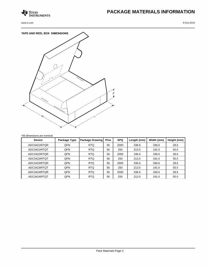
*All dimensions are nominal
Device Package Type Package Drawing Pins SPQ Length (mm) Width (mm) Height (mm)
ADC3421IRTQR QFN RTQ 56 2000 336.6 336.6 28.6
ADC3421IRTQT QFN RTQ 56 250 213.0 191.0 55.0
ADC3422IRTQR QFN RTQ 56 2000 336.6 336.6 28.6
ADC3422IRTQT QFN RTQ 56 250 213.0 191.0 55.0
ADC3423IRTQR QFN RTQ 56 2000 336.6 336.6 28.6
ADC3423IRTQT QFN RTQ 56 250 213.0 191.0 55.0
ADC3424IRTQR QFN RTQ 56 2000 336.6 336.6 28.6
ADC3424IRTQT QFN RTQ 56 250 213.0 191.0 55.0
PACKAGE MATERIALS INFORMATION
www.ti.com 9-Oct-2015
Pack Materials-Page 2

IMPORTANT NOTICE
Texas Instruments Incorporated (TI) reserves the right to make corrections, enhancements, improvements and other changes to itssemiconductor products and services per JESD46, latest issue, and to discontinue any product or service per JESD48, latest issue. Buyersshould obtain the latest relevant information before placing orders and should verify that such information is current and complete.TI’s published terms of sale for semiconductor products (http://www.ti.com/sc/docs/stdterms.htm) apply to the sale of packaged integratedcircuit products that TI has qualified and released to market. Additional terms may apply to the use or sale of other types of TI products andservices.Reproduction of significant portions of TI information in TI data sheets is permissible only if reproduction is without alteration and isaccompanied by all associated warranties, conditions, limitations, and notices. TI is not responsible or liable for such reproduceddocumentation. Information of third parties may be subject to additional restrictions. Resale of TI products or services with statementsdifferent from or beyond the parameters stated by TI for that product or service voids all express and any implied warranties for theassociated TI product or service and is an unfair and deceptive business practice. TI is not responsible or liable for any such statements.Buyers and others who are developing systems that incorporate TI products (collectively, “Designers”) understand and agree that Designersremain responsible for using their independent analysis, evaluation and judgment in designing their applications and that Designers havefull and exclusive responsibility to assure the safety of Designers' applications and compliance of their applications (and of all TI productsused in or for Designers’ applications) with all applicable regulations, laws and other applicable requirements. Designer represents that, withrespect to their applications, Designer has all the necessary expertise to create and implement safeguards that (1) anticipate dangerousconsequences of failures, (2) monitor failures and their consequences, and (3) lessen the likelihood of failures that might cause harm andtake appropriate actions. Designer agrees that prior to using or distributing any applications that include TI products, Designer willthoroughly test such applications and the functionality of such TI products as used in such applications.TI’s provision of technical, application or other design advice, quality characterization, reliability data or other services or information,including, but not limited to, reference designs and materials relating to evaluation modules, (collectively, “TI Resources”) are intended toassist designers who are developing applications that incorporate TI products; by downloading, accessing or using TI Resources in anyway, Designer (individually or, if Designer is acting on behalf of a company, Designer’s company) agrees to use any particular TI Resourcesolely for this purpose and subject to the terms of this Notice.TI’s provision of TI Resources does not expand or otherwise alter TI’s applicable published warranties or warranty disclaimers for TIproducts, and no additional obligations or liabilities arise from TI providing such TI Resources. TI reserves the right to make corrections,enhancements, improvements and other changes to its TI Resources. TI has not conducted any testing other than that specificallydescribed in the published documentation for a particular TI Resource.Designer is authorized to use, copy and modify any individual TI Resource only in connection with the development of applications thatinclude the TI product(s) identified in such TI Resource. NO OTHER LICENSE, EXPRESS OR IMPLIED, BY ESTOPPEL OR OTHERWISETO ANY OTHER TI INTELLECTUAL PROPERTY RIGHT, AND NO LICENSE TO ANY TECHNOLOGY OR INTELLECTUAL PROPERTYRIGHT OF TI OR ANY THIRD PARTY IS GRANTED HEREIN, including but not limited to any patent right, copyright, mask work right, orother intellectual property right relating to any combination, machine, or process in which TI products or services are used. Informationregarding or referencing third-party products or services does not constitute a license to use such products or services, or a warranty orendorsement thereof. Use of TI Resources may require a license from a third party under the patents or other intellectual property of thethird party, or a license from TI under the patents or other intellectual property of TI.TI RESOURCES ARE PROVIDED “AS IS” AND WITH ALL FAULTS. TI DISCLAIMS ALL OTHER WARRANTIES ORREPRESENTATIONS, EXPRESS OR IMPLIED, REGARDING RESOURCES OR USE THEREOF, INCLUDING BUT NOT LIMITED TOACCURACY OR COMPLETENESS, TITLE, ANY EPIDEMIC FAILURE WARRANTY AND ANY IMPLIED WARRANTIES OFMERCHANTABILITY, FITNESS FOR A PARTICULAR PURPOSE, AND NON-INFRINGEMENT OF ANY THIRD PARTY INTELLECTUALPROPERTY RIGHTS. TI SHALL NOT BE LIABLE FOR AND SHALL NOT DEFEND OR INDEMNIFY DESIGNER AGAINST ANY CLAIM,INCLUDING BUT NOT LIMITED TO ANY INFRINGEMENT CLAIM THAT RELATES TO OR IS BASED ON ANY COMBINATION OFPRODUCTS EVEN IF DESCRIBED IN TI RESOURCES OR OTHERWISE. IN NO EVENT SHALL TI BE LIABLE FOR ANY ACTUAL,DIRECT, SPECIAL, COLLATERAL, INDIRECT, PUNITIVE, INCIDENTAL, CONSEQUENTIAL OR EXEMPLARY DAMAGES INCONNECTION WITH OR ARISING OUT OF TI RESOURCES OR USE THEREOF, AND REGARDLESS OF WHETHER TI HAS BEENADVISED OF THE POSSIBILITY OF SUCH DAMAGES.Unless TI has explicitly designated an individual product as meeting the requirements of a particular industry standard (e.g., ISO/TS 16949and ISO 26262), TI is not responsible for any failure to meet such industry standard requirements.Where TI specifically promotes products as facilitating functional safety or as compliant with industry functional safety standards, suchproducts are intended to help enable customers to design and create their own applications that meet applicable functional safety standardsand requirements. Using products in an application does not by itself establish any safety features in the application. Designers mustensure compliance with safety-related requirements and standards applicable to their applications. Designer may not use any TI products inlife-critical medical equipment unless authorized officers of the parties have executed a special contract specifically governing such use.Life-critical medical equipment is medical equipment where failure of such equipment would cause serious bodily injury or death (e.g., lifesupport, pacemakers, defibrillators, heart pumps, neurostimulators, and implantables). Such equipment includes, without limitation, allmedical devices identified by the U.S. Food and Drug Administration as Class III devices and equivalent classifications outside the U.S.TI may expressly designate certain products as completing a particular qualification (e.g., Q100, Military Grade, or Enhanced Product).Designers agree that it has the necessary expertise to select the product with the appropriate qualification designation for their applicationsand that proper product selection is at Designers’ own risk. Designers are solely responsible for compliance with all legal and regulatoryrequirements in connection with such selection.Designer will fully indemnify TI and its representatives against any damages, costs, losses, and/or liabilities arising out of Designer’s non-compliance with the terms and provisions of this Notice.
Mailing Address: Texas Instruments, Post Office Box 655303, Dallas, Texas 75265Copyright © 2017, Texas Instruments Incorporated