Embed Size (px)
Citation preview
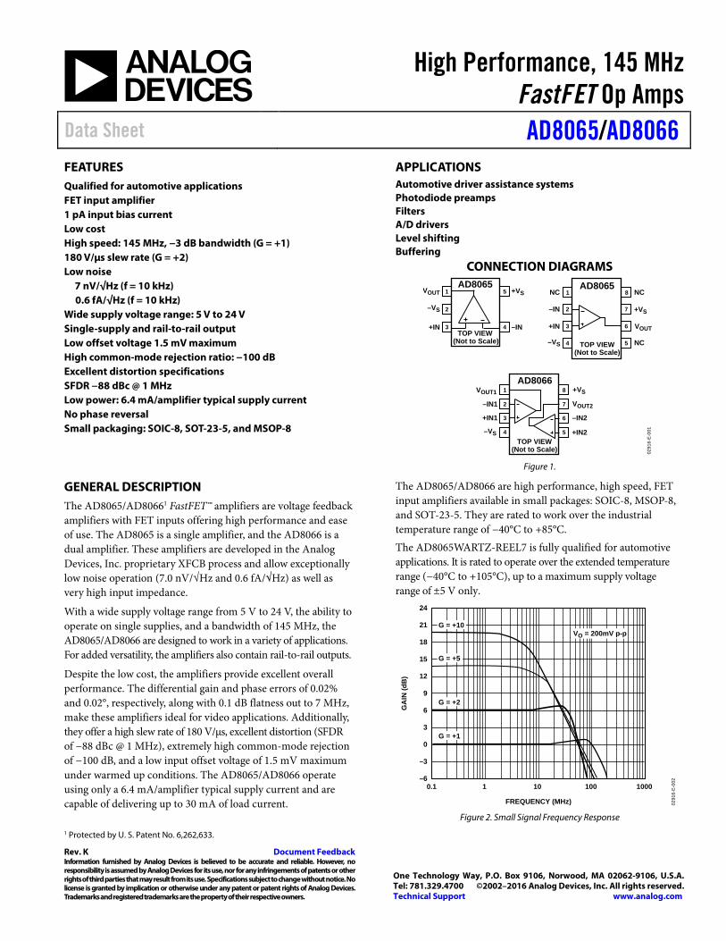
High Performance, 145 MHz FastFET Op Amps
Data Sheet AD8065/AD8066
Rev. K Document Feedback Information furnished by Analog Devices is believed to be accurate and reliable. However, no responsibility is assumed by Analog Devices for its use, nor for any infringements of patents or other rights of third parties that may result from its use. Specifications subject to change without notice. No license is granted by implication or otherwise under any patent or patent rights of Analog Devices. Trademarks and registered trademarks are the property of their respective owners.
One Technology Way, P.O. Box 9106, Norwood, MA 02062-9106, U.S.A. Tel: 781.329.4700 ©2002–2016 Analog Devices, Inc. All rights reserved. Technical Support www.analog.com
FEATURES Qualified for automotive applications FET input amplifier 1 pA input bias current Low cost High speed: 145 MHz, −3 dB bandwidth (G = +1) 180 V/µs slew rate (G = +2) Low noise
7 nV/√Hz (f = 10 kHz) 0.6 fA/√Hz (f = 10 kHz)
Wide supply voltage range: 5 V to 24 V Single-supply and rail-to-rail output Low offset voltage 1.5 mV maximum High common-mode rejection ratio: −100 dB Excellent distortion specifications SFDR −88 dBc @ 1 MHz Low power: 6.4 mA/amplifier typical supply current No phase reversal Small packaging: SOIC-8, SOT-23-5, and MSOP-8
APPLICATIONS Automotive driver assistance systems Photodiode preamps Filters A/D drivers Level shifting Buffering
CONNECTION DIAGRAMS
1
2
3
5
4
1
4
3
5
2 7
8
6
8
7
6
5
1
2
3
4
VOUT
VOUT1
VOUT2
VOUT
–VS
–VS
–VS
+IN
+VS
+VS
+VS
–IN
–IN1
+IN1 –IN2
+IN2
NC
–IN
+IN
NC
NC
TOP VIEW(Not to Scale)
TOP VIEW(Not to Scale)
TOP VIEW(Not to Scale)
AD8065
AD8066
AD8065
0291
6-E
-001
Figure 1.
GENERAL DESCRIPTION The AD8065/AD80661 FastFET™ amplifiers are voltage feedback amplifiers with FET inputs offering high performance and ease of use. The AD8065 is a single amplifier, and the AD8066 is a dual amplifier. These amplifiers are developed in the Analog Devices, Inc. proprietary XFCB process and allow exceptionally low noise operation (7.0 nV/√Hz and 0.6 fA/√Hz) as well as very high input impedance.
With a wide supply voltage range from 5 V to 24 V, the ability to operate on single supplies, and a bandwidth of 145 MHz, the AD8065/AD8066 are designed to work in a variety of applications. For added versatility, the amplifiers also contain rail-to-rail outputs.
Despite the low cost, the amplifiers provide excellent overall performance. The differential gain and phase errors of 0.02% and 0.02°, respectively, along with 0.1 dB flatness out to 7 MHz, make these amplifiers ideal for video applications. Additionally, they offer a high slew rate of 180 V/µs, excellent distortion (SFDR of −88 dBc @ 1 MHz), extremely high common-mode rejection of −100 dB, and a low input offset voltage of 1.5 mV maximum under warmed up conditions. The AD8065/AD8066 operate using only a 6.4 mA/amplifier typical supply current and are capable of delivering up to 30 mA of load current.
The AD8065/AD8066 are high performance, high speed, FET input amplifiers available in small packages: SOIC-8, MSOP-8, and SOT-23-5. They are rated to work over the industrial temperature range of −40°C to +85°C.
The AD8065WARTZ-REEL7 is fully qualified for automotive applications. It is rated to operate over the extended temperature range (−40°C to +105°C), up to a maximum supply voltage range of ±5 V only.
–6
–3
0
3
6
9
12
15
18
21
24
GA
IN (d
B)
FREQUENCY (MHz)
10.1 10 100 1000
0291
6-E
-002
G = +10VO = 200mV p-p
G = +5
G = +2
G = +1
Figure 2. Small Signal Frequency Response
1 Protected by U. S. Patent No. 6,262,633.

AD8065/AD8066 Data Sheet
Rev. K | Page 2 of 28
TABLE OF CONTENTS Features .............................................................................................. 1 Applications ....................................................................................... 1 Connection Diagrams ...................................................................... 1 General Description ......................................................................... 1 Revision History ............................................................................... 3 Specifications ±5 V ........................................................................... 4 Specifications ±12 V ......................................................................... 6 Specifications +5 V ........................................................................... 7 Absolute Maximum Ratings ............................................................ 9
Maximum Power Dissipation ..................................................... 9 Output Short Circuit .................................................................... 9 ESD Caution .................................................................................. 9
Typical Performance Characteristics ........................................... 10 Test Circuits ..................................................................................... 17 Theory of Operation ...................................................................... 20
Closed-Loop Frequency Response ........................................... 20 Noninverting Closed-Loop Frequency Response .................. 20 Inverting Closed-Loop Frequency Response ......................... 20
Wideband Operation ................................................................. 21 Input Protection ......................................................................... 21 Thermal Considerations ............................................................ 22 Input and Output Overload Behavior ..................................... 22
Layout, Grounding, and Bypassing Considerations .................. 23 Power Supply Bypassing ............................................................ 23 Grounding ................................................................................... 23 Leakage Currents ........................................................................ 23 Input Capacitance ...................................................................... 23 Output Capacitance ................................................................... 23 Input-to-Output Coupling ........................................................ 24 Wideband Photodiode Preamp ................................................ 24 High Speed JFET Input Instrumentation Amplifier.............. 25 Video Buffer ................................................................................ 26
Outline Dimensions ....................................................................... 27 Ordering Guide .......................................................................... 28 Automotive Products ................................................................. 28
Data Sheet AD8065/AD8066
Rev. K | Page 3 of 28
REVISION HISTORY
8/2016—Rev. K to Rev. J Updated Outline Dimensions ........................................................ 27 Changes to Ordering Guide ........................................................... 28
8/2010—Rev. I to Rev. J Changes to Features Section, Applications Section, and General Description Section ........................................................................... 1 Change to Table 1 .............................................................................. 4 Change to Table 3 .............................................................................. 7 Changes to Table 4 ............................................................................ 9 Changes to Figure 9......................................................................... 10 Changes to Inverting Closed-Loop Frequency Response Section .............................................................................................. 20 Moved Leakage Currents Section, Input Capacitance Section, and Output Capacitance Section ................................................... 23 Moved Input-to-Input Coupling Section, Wideband Photodiode Preamp Section, and Figure 59 ................................ 24 Changes to Table 5 .......................................................................... 25 Moved Figure 60 and High Speed JFET Input Instrumentation Amplifier Section ............................................................................ 25 Updated Outline Dimensions ........................................................ 27 Changes to Ordering Guide ........................................................... 28 Added Automotive Products Section ........................................... 28 3/2009—Rev. H to Rev. I Changes to High Speed JFET Input Instrumentation Amplifier Section .............................................................................................. 23 Updated Outline Dimensions ........................................................ 24
9/2008—Rev. G to Rev. H Deleted Usable Range Parameter, Table 1 ...................................... 3 Deleted Usable Range Parameter, Table 2 ...................................... 4 Deleted Usable Range Parameter, Table 3 ...................................... 5 Changes to Layout ............................................................................. 6 Changes to Input and Output Overload Behavior Section ........ 19 Changes to Table 5 Expressions Column ..................................... 22
1/2006—Rev. F to Rev. G Changes to Ordering Guide ........................................................... 26
12/2005—Rev. E to Rev. F Updated Format.................................................................. Universal Changes to Features .......................................................................... 1 Changes to General Description ..................................................... 1
Changes to Figure 22 through Figure 27...................................... 11 Updated Outline Dimensions........................................................ 25 Changes to Ordering Guide ........................................................... 26
2/2004—Rev. D to Rev. E. Updated Format ................................................................ Universal Updated Figure 56 ......................................................................... 21 Updated Outline Dimensions...................................................... 25 Updated Ordering Guide ............................................................. 26
11/2003—Rev. C to Rev. D. Changes to Features ......................................................................... 1 Changes to Connection Diagrams ................................................. 1 Updated Ordering Guide ................................................................ 5 Updated Outline Dimensions...................................................... 22
4/2003—Rev. B to Rev. C. Added SOIC-8 (R) for the AD8065 ............................................... 4
2/2003—Rev. A to Rev. B. Changes to Absolute Maximum Ratings....................................... 4 Changes to Test Circuit 10 ........................................................... 14 Changes to Test Circuit 11 ........................................................... 15 Changes to Noninverting Closed-Loop Frequency Response 16 Changes to Inverting Closed-Loop Frequency Response ....... 16 Updated Figure 6 .......................................................................... 18 Changes to Figure 7 ...................................................................... 19 Changes to Figure 10 .................................................................... 21 Changes to Figure 11 .................................................................... 22 Changes to High Speed JFET Instrumentation Amplifier ...... 22 Changes to Video Buffer .............................................................. 22
8/2002—Rev. 0 to Rev. A. Added AD8066 .................................................................. Universal Added SOIC-8 (R) and MSOP-8 (RM) ......................................... 1 Edits to General Description .......................................................... 1 Edits to Specifications ...................................................................... 2 New Figure 2 ..................................................................................... 5 Changes to Ordering Guide ............................................................ 5 Edits to TPCs 18, 25, and 28 ........................................................... 8 New TPC 36 ................................................................................... 11 Added Test Circuits 10 and 11 .................................................... 14 MSOP (RM-8) Added .................................................................. 23

AD8065/AD8066 Data Sheet
Rev. K | Page 4 of 28
SPECIFICATIONS ±5 V @ TA = 25°C, VS = ±5 V, RL = 1 kΩ, unless otherwise noted.
Table 1. Parameter Conditions Min Typ Max Unit DYNAMIC PERFORMANCE
−3 dB Bandwidth G = +1, VO = 0.2 V p-p (AD8065) 100 145 MHz AD8065WARTZ only: TMIN − TMAX 88 MHz G = +1, VO = 0.2 V p-p (AD8066) 100 120 MHz G = +2, VO = 0.2 V p-p 50 MHz G = +2, VO = 2 V p-p 42 MHz Bandwidth for 0.1 dB Flatness G = +2, VO = 0.2 V p-p 7 MHz Input Overdrive Recovery Time G = +1, −5.5 V to +5.5 V 175 ns Output Recovery Time G = −1, −5.5 V to +5.5 V 170 ns Slew Rate G = +2, VO = 4 V step 130 180 V/µs AD8065WARTZ only: TMIN − TMAX 155 V/µs Settling Time to 0.1% G = +2, VO = 2 V step 55 ns
G = +2, VO = 8 V step 205 ns NOISE/HARMONIC PERFORMANCE
SFDR fC = 1 MHz, G = +2, VO = 2 V p-p −88 dBc fC = 5 MHz, G = +2, VO = 2 V p-p −67 dBc fC = 1 MHz, G = +2, VO = 8 V p-p −73 dBc Third-Order Intercept fC = 10 MHz, RL = 100 Ω 24 dBm Input Voltage Noise f = 10 kHz 7 nV/√Hz Input Current Noise f = 10 kHz 0.6 fA/√Hz Differential Gain Error NTSC, G = +2, RL = 150 Ω 0.02 % Differential Phase Error NTSC, G = +2, RL = 150 Ω 0.02 Degrees
DC PERFORMANCE Input Offset Voltage VCM = 0 V, SOIC package 0.4 1.5 mV AD8065WARTZ only: TMIN − TMAX 2.6 mV Input Offset Voltage Drift 1 17 µV/°C AD8065WARTZ only: TMIN − TMAX 17 µV/°C Input Bias Current SOIC package 2 6 pA TMIN to TMAX 25 125 pA Input Offset Current 1 10 pA TMIN to TMAX 1 125 pA Open-Loop Gain VO = ±3 V, RL = 1 kΩ 100 113 dB AD8065WARTZ only: TMIN − TMAX 100 dB
INPUT CHARACTERISTICS Common-Mode Input Impedance 1000 || 2.1 GΩ || pF Differential Input Impedance 1000 || 4.5 GΩ || pF Input Common-Mode Voltage Range
FET Input Range −5 to +1.7 −5.0 to +2.4 V AD8065WARTZ only: TMIN − TMAX −5 to +1.7 V
Common-Mode Rejection Ratio VCM = −1 V to +1 V −85 −100 dB VCM = −1 V to +1 V (SOT-23) −82 −91 dB AD8065WARTZ only: TMIN − TMAX −82 dB
Data Sheet AD8065/AD8066
Rev. K | Page 5 of 28
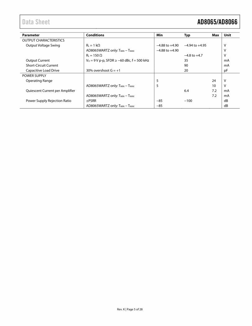
Parameter Conditions Min Typ Max Unit OUTPUT CHARACTERISTICS
Output Voltage Swing RL = 1 kΩ −4.88 to +4.90 −4.94 to +4.95 V AD8065WARTZ only: TMIN − TMAX −4.88 to +4.90 V RL = 150 Ω −4.8 to +4.7 V Output Current VO = 9 V p-p, SFDR ≥ −60 dBc, f = 500 kHz 35 mA Short-Circuit Current 90 mA Capacitive Load Drive 30% overshoot G = +1 20 pF
POWER SUPPLY Operating Range 5 24 V AD8065WARTZ only: TMIN − TMAX 5 10 V Quiescent Current per Amplifier 6.4 7.2 mA AD8065WARTZ only: TMIN − TMAX 7.2 mA Power Supply Rejection Ratio ±PSRR −85 −100 dB AD8065WARTZ only: TMIN − TMAX −85 dB
AD8065/AD8066 Data Sheet
Rev. K | Page 6 of 28
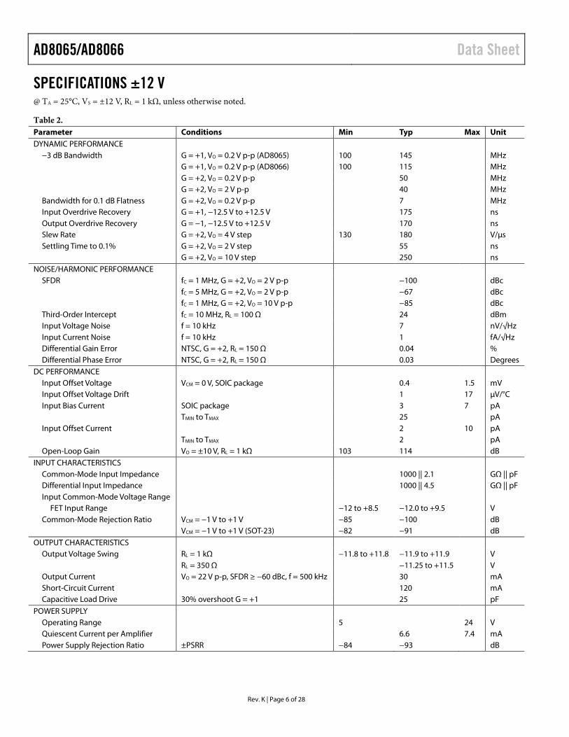
SPECIFICATIONS ±12 V @ TA = 25°C, VS = ±12 V, RL = 1 kΩ, unless otherwise noted.
Table 2. Parameter Conditions Min Typ Max Unit DYNAMIC PERFORMANCE
−3 dB Bandwidth G = +1, VO = 0.2 V p-p (AD8065) 100 145 MHz G = +1, VO = 0.2 V p-p (AD8066) 100 115 MHz G = +2, VO = 0.2 V p-p 50 MHz G = +2, VO = 2 V p-p 40 MHz Bandwidth for 0.1 dB Flatness G = +2, VO = 0.2 V p-p 7 MHz Input Overdrive Recovery G = +1, −12.5 V to +12.5 V 175 ns Output Overdrive Recovery G = −1, −12.5 V to +12.5 V 170 ns Slew Rate G = +2, VO = 4 V step 130 180 V/µs Settling Time to 0.1% G = +2, VO = 2 V step 55 ns
G = +2, VO = 10 V step 250 ns NOISE/HARMONIC PERFORMANCE
SFDR fC = 1 MHz, G = +2, VO = 2 V p-p −100 dBc fC = 5 MHz, G = +2, VO = 2 V p-p −67 dBc fC = 1 MHz, G = +2, VO = 10 V p-p −85 dBc
Third-Order Intercept fC = 10 MHz, RL = 100 Ω 24 dBm Input Voltage Noise f = 10 kHz 7 nV/√Hz Input Current Noise f = 10 kHz 1 fA/√Hz Differential Gain Error NTSC, G = +2, RL = 150 Ω 0.04 % Differential Phase Error NTSC, G = +2, RL = 150 Ω 0.03 Degrees
DC PERFORMANCE Input Offset Voltage VCM = 0 V, SOIC package 0.4 1.5 mV Input Offset Voltage Drift 1 17 µV/°C Input Bias Current SOIC package 3 7 pA TMIN to TMAX 25 pA Input Offset Current 2 10 pA TMIN to TMAX 2 pA Open-Loop Gain VO = ±10 V, RL = 1 kΩ 103 114 dB
INPUT CHARACTERISTICS Common-Mode Input Impedance 1000 || 2.1 GΩ || pF Differential Input Impedance 1000 || 4.5 GΩ || pF Input Common-Mode Voltage Range
FET Input Range −12 to +8.5 −12.0 to +9.5 V Common-Mode Rejection Ratio VCM = −1 V to +1 V −85 −100 dB
VCM = −1 V to +1 V (SOT-23) −82 −91 dB OUTPUT CHARACTERISTICS
Output Voltage Swing RL = 1 kΩ −11.8 to +11.8 −11.9 to +11.9 V RL = 350 Ω −11.25 to +11.5 V Output Current VO = 22 V p-p, SFDR ≥ −60 dBc, f = 500 kHz 30 mA Short-Circuit Current 120 mA Capacitive Load Drive 30% overshoot G = +1 25 pF
POWER SUPPLY Operating Range 5 24 V Quiescent Current per Amplifier 6.6 7.4 mA Power Supply Rejection Ratio ±PSRR −84 −93 dB
Data Sheet AD8065/AD8066
Rev. K | Page 7 of 28
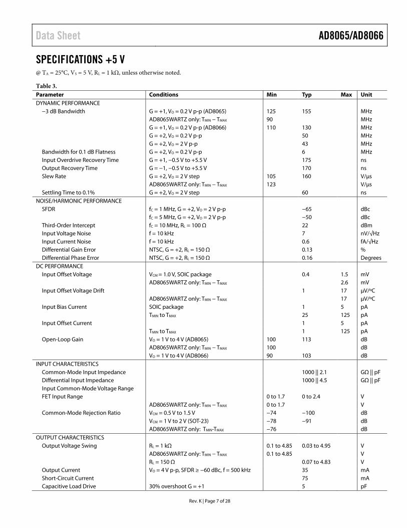
SPECIFICATIONS +5 V @ TA = 25°C, VS = 5 V, RL = 1 kΩ, unless otherwise noted.
Table 3. Parameter Conditions Min Typ Max Unit DYNAMIC PERFORMANCE
−3 dB Bandwidth G = +1, VO = 0.2 V p-p (AD8065) 125 155 MHz AD8065WARTZ only: TMIN − TMAX 90 MHz G = +1, VO = 0.2 V p-p (AD8066) 110 130 MHz G = +2, VO = 0.2 V p-p 50 MHz G = +2, VO = 2 V p-p 43 MHz Bandwidth for 0.1 dB Flatness G = +2, VO = 0.2 V p-p 6 MHz Input Overdrive Recovery Time G = +1, −0.5 V to +5.5 V 175 ns Output Recovery Time G = −1, −0.5 V to +5.5 V 170 ns Slew Rate G = +2, VO = 2 V step 105 160 V/µs AD8065WARTZ only: TMIN − TMAX 123 V/µs Settling Time to 0.1% G = +2, VO = 2 V step 60 ns
NOISE/HARMONIC PERFORMANCE SFDR fC = 1 MHz, G = +2, VO = 2 V p-p −65 dBc fC = 5 MHz, G = +2, VO = 2 V p-p −50 dBc Third-Order Intercept fC = 10 MHz, RL = 100 Ω 22 dBm Input Voltage Noise f = 10 kHz 7 nV/√Hz Input Current Noise f = 10 kHz 0.6 fA/√Hz Differential Gain Error NTSC, G = +2, RL = 150 Ω 0.13 % Differential Phase Error NTSC, G = +2, RL = 150 Ω 0.16 Degrees
DC PERFORMANCE Input Offset Voltage VCM = 1.0 V, SOIC package 0.4 1.5 mV AD8065WARTZ only: TMIN − TMAX 2.6 mV Input Offset Voltage Drift 1 17 µV/ºC AD8065WARTZ only: TMIN − TMAX 17 µV/ºC Input Bias Current SOIC package 1 5 pA TMIN to TMAX 25 125 pA Input Offset Current 1 5 pA TMIN to TMAX 1 125 pA Open-Loop Gain VO = 1 V to 4 V (AD8065) 100 113 dB AD8065WARTZ only: TMIN − TMAX 100 dB
VO = 1 V to 4 V (AD8066) 90 103 dB INPUT CHARACTERISTICS
Common-Mode Input Impedance 1000 || 2.1 GΩ || pF Differential Input Impedance 1000 || 4.5 GΩ || pF Input Common-Mode Voltage Range FET Input Range 0 to 1.7 0 to 2.4 V AD8065WARTZ only: TMIN − TMAX 0 to 1.7 V Common-Mode Rejection Ratio VCM = 0.5 V to 1.5 V −74 −100 dB
VCM = 1 V to 2 V (SOT-23) −78 −91 dB AD8065WARTZ only: TMIN-TMAX −76 dB OUTPUT CHARACTERISTICS
Output Voltage Swing RL = 1 kΩ 0.1 to 4.85 0.03 to 4.95 V AD8065WARTZ only: TMIN − TMAX 0.1 to 4.85 V RL = 150 Ω 0.07 to 4.83 V Output Current VO = 4 V p-p, SFDR ≥ −60 dBc, f = 500 kHz 35 mA Short-Circuit Current 75 mA Capacitive Load Drive 30% overshoot G = +1 5 pF
AD8065/AD8066 Data Sheet
Rev. K | Page 8 of 28
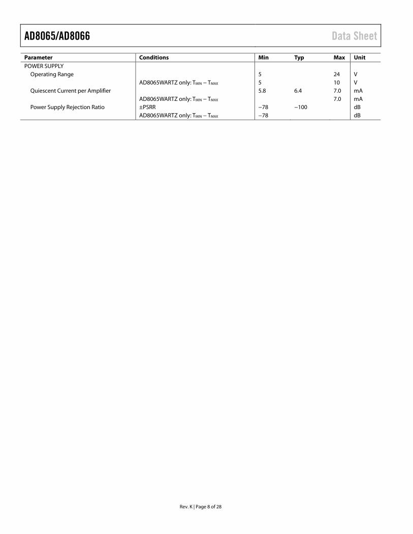
Parameter Conditions Min Typ Max Unit POWER SUPPLY
Operating Range 5 24 V AD8065WARTZ only: TMIN − TMAX 5 10 V Quiescent Current per Amplifier 5.8 6.4 7.0 mA AD8065WARTZ only: TMIN − TMAX 7.0 mA Power Supply Rejection Ratio ±PSRR −78 −100 dB AD8065WARTZ only: TMIN − TMAX −78 dB
Data Sheet AD8065/AD8066
Rev. K | Page 9 of 28
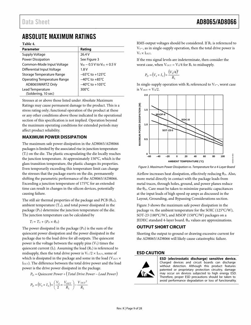
ABSOLUTE MAXIMUM RATINGS Table 4. Parameter Rating Supply Voltage 26.4 V Power Dissipation See Figure 3 Common-Mode Input Voltage VEE − 0.5 V to VCC + 0.5 V Differential Input Voltage 1.8 V Storage Temperature Range −65°C to +125°C Operating Temperature Range −40°C to +85°C
AD8065WARTZ Only −40°C to +105°C Lead Temperature
(Soldering, 10 sec) 300°C
Stresses at or above those listed under Absolute Maximum Ratings may cause permanent damage to the product. This is a stress rating only; functional operation of the product at these or any other conditions above those indicated in the operational section of this specification is not implied. Operation beyond the maximum operating conditions for extended periods may affect product reliability.
MAXIMUM POWER DISSIPATION The maximum safe power dissipation in the AD8065/AD8066 packages is limited by the associated rise in junction temperature (TJ) on the die. The plastic encapsulating the die locally reaches the junction temperature. At approximately 150°C, which is the glass transition temperature, the plastic changes its properties. Even temporarily exceeding this temperature limit can change the stresses that the package exerts on the die, permanently shifting the parametric performance of the AD8065/AD8066. Exceeding a junction temperature of 175°C for an extended time can result in changes in the silicon devices, potentially causing failure.
The still air thermal properties of the package and PCB (θJA), ambient temperature (TA), and total power dissipated in the package (PD) determine the junction temperature of the die. The junction temperature can be calculated by
TJ = TA + (PD × θJA)
The power dissipated in the package (PD) is the sum of the quiescent power dissipation and the power dissipated in the package due to the load drive for all outputs. The quiescent power is the voltage between the supply pins (VS) times the quiescent current (IS). Assuming the load (RL) is referenced to midsupply, then the total drive power is VS /2 × IOUT, some of which is dissipated in the package and some in the load (VOUT × IOUT). The difference between the total drive power and the load power is the drive power dissipated in the package.
( )PowerLoadPowerDriveTotalPowerQuiescentPD −+=
( )L
OUT
L
OUTSSSD R
VR
VVIVP
2
2−
×+×=
RMS output voltages should be considered. If RL is referenced to VS−, as in single-supply operation, then the total drive power is VS × IOUT.
If the rms signal levels are indeterminate, then consider the worst case, when VOUT = VS/4 for RL to midsupply.
( ) ( )L
SSSD R
VIVP
24/+×=
In single-supply operation with RL referenced to VS−, worst case is VOUT = VS/2.
MA
XIM
UM
PO
WER
DIS
SIPA
TIO
N (W
)
0
0.5
1.0
1.5
2.0
200–40 –20–60 40 60 80 100
AMBIENT TEMPERATURE (°C) 0291
6-E
-003
MSOP-8
SOIC-8
SOT-23-5
Figure 3. Maximum Power Dissipation vs. Temperature for a 4-Layer Board
Airflow increases heat dissipation, effectively reducing θJA. Also, more metal directly in contact with the package leads from metal traces, through holes, ground, and power planes reduce the θJA. Care must be taken to minimize parasitic capacitances at the input leads of high speed op amps as discussed in the Layout, Grounding, and Bypassing Considerations section.
Figure 3 shows the maximum safe power dissipation in the package vs. the ambient temperature for the SOIC (125°C/W), SOT-23 (180°C/W), and MSOP (150°C/W) packages on a JEDEC standard 4-layer board. θJA values are approximations.
OUTPUT SHORT CIRCUIT Shorting the output to ground or drawing excessive current for the AD8065/AD8066 will likely cause catastrophic failure.
ESD CAUTION
AD8065/AD8066 Data Sheet
Rev. K | Page 10 of 28
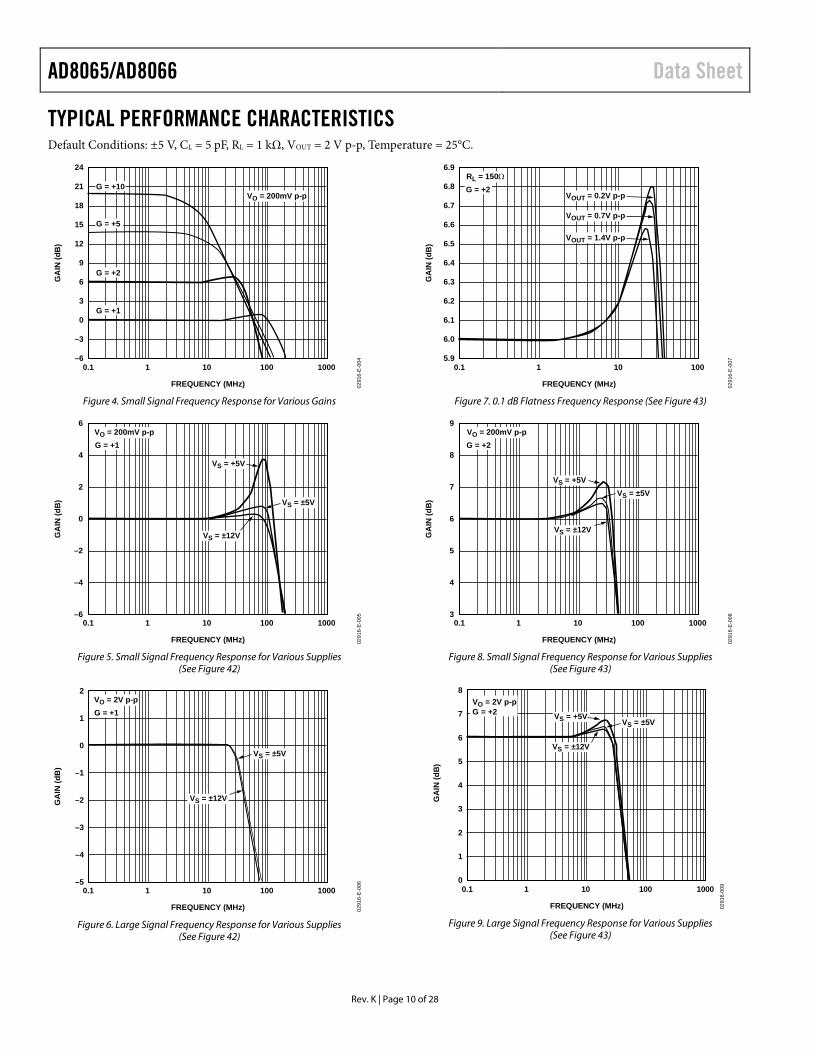
TYPICAL PERFORMANCE CHARACTERISTICS Default Conditions: ±5 V, CL = 5 pF, RL = 1 kΩ, VOUT = 2 V p-p, Temperature = 25°C.
–6
–3
0
3
6
9
12
15
18
21
24
GA
IN (d
B)
FREQUENCY (MHz)
10.1 10 100 100002
916-
E-0
04
G = +10VO = 200mV p-p
G = +5
G = +2
G = +1
Figure 4. Small Signal Frequency Response for Various Gains
–6
–4
–2
0
2
4
6
GA
IN (d
B)
FREQUENCY (MHz)
10.1 10 100 1000
0291
6-E
-005
VO = 200mV p-pG = +1
VS = +5V
VS = ±12V
VS = ±5V
Figure 5. Small Signal Frequency Response for Various Supplies
(See Figure 42)
–5
–4
–3
–2
–1
0
1
2
GA
IN (d
B)
FREQUENCY (MHz)
10.1 10 100 1000
0291
6-E
-006
VO = 2V p-pG = +1
VS = ±12V
VS = ±5V
Figure 6. Large Signal Frequency Response for Various Supplies
(See Figure 42)
5.9
6.0
6.1
6.2
6.3
6.4
6.5
6.6
6.7
6.8
6.9
GA
IN (d
B)
FREQUENCY (MHz)
0.1 101 100
0291
6-E
-007
RL = 150ΩG = +2
VOUT = 0.2V p-p
VOUT = 0.7V p-p
VOUT = 1.4V p-p
Figure 7. 0.1 dB Flatness Frequency Response (See Figure 43)
3
4
5
6
7
8
9G
AIN
(dB
)
FREQUENCY (MHz)
10.1 10 100 1000
0291
6-E
-008
VO = 200mV p-pG = +2
VS = ±12V
VS = ±5VVS = +5V
Figure 8. Small Signal Frequency Response for Various Supplies
(See Figure 43)
0
1
2
3
4
5
GA
IN (d
B)
6
7
8
FREQUENCY (MHz)
10.1 10 100 1000
0291
6-00
9
G = +2
VS = ±12V
VS = ±5VVS = +5V
VO = 2V p-p
Figure 9. Large Signal Frequency Response for Various Supplies
(See Figure 43)
Data Sheet AD8065/AD8066
Rev. K | Page 11 of 28
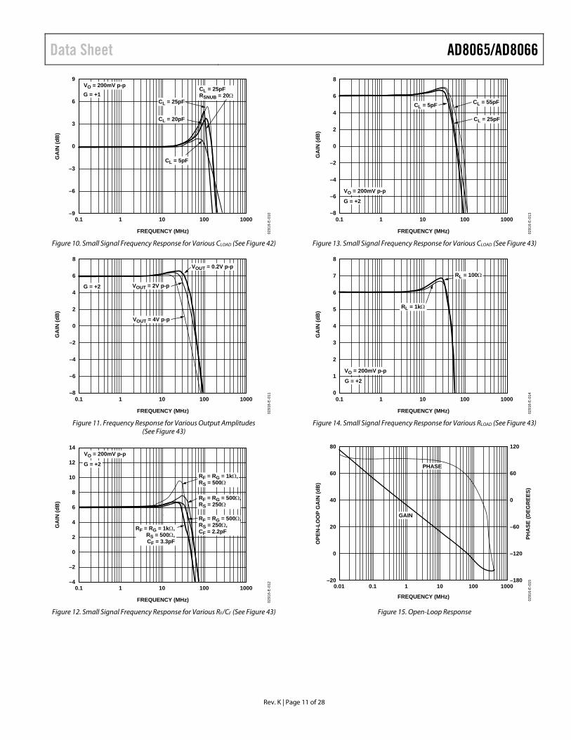
–9
–6
–3
0
3
6
9
GA
IN (d
B)
FREQUENCY (MHz)
10.1 10 100 1000
0291
6-E
-010
G = +1CL = 25pF
CL = 25pFRSNUB = 20Ω
CL = 20pF
CL = 5pF
VO = 200mV p-p
Figure 10. Small Signal Frequency Response for Various CLOAD (See Figure 42)
–8
–6
–4
–2
0
2
GA
IN (d
B)
4
6
8
FREQUENCY (MHz)
10.1 10 100 1000
0291
6-E
-011
G = +2
VOUT = 0.2V p-p
VOUT = 2V p-p
VOUT = 4V p-p
Figure 11. Frequency Response for Various Output Amplitudes
(See Figure 43)
–4
–2
0
2
4
6
8
10
12
14
GA
IN (d
B)
FREQUENCY (MHz)
10.1 10 100 1000
0291
6-E
-012
G = +2
RF = RG = 1kΩ,RS = 500Ω
RF = RG = 500Ω,RS = 250Ω
RF = RG = 500Ω,RS = 250Ω,CF = 2.2pFRF = RG = 1kΩ,
RS = 500Ω,CF = 3.3pF
VO = 200mV p-p
Figure 12. Small Signal Frequency Response for Various RF/CF (See Figure 43)
–8
–6
–4
–2
0
2
GA
IN (d
B)
4
6
8
FREQUENCY (MHz)
10.1 10 100 1000
0291
6-E
-013
CL = 25pF
CL = 55pFCL = 5pF
VO = 200mV p-p
G = +2
Figure 13. Small Signal Frequency Response for Various CLOAD (See Figure 43)
0
1
2
3
4
5G
AIN
(dB
)
6
7
8
FREQUENCY (MHz)
10.1 10 100 1000
0291
6-E
-014
RL = 100Ω
RL = 1kΩ
VO = 200mV p-p
G = +2
Figure 14. Small Signal Frequency Response for Various RLOAD (See Figure 43)
–180
–120
–60
0
60
120
PHA
SE (D
EGR
EES)
–20
0
20
40
60
80
OPE
N-L
OO
P G
AIN
(dB
)
0.01 0.1 1 10 100 1000
FREQUENCY (MHz)
0291
6-E-
015
PHASE
GAIN
Figure 15. Open-Loop Response
AD8065/AD8066 Data Sheet
Rev. K | Page 12 of 28
–120
–110
–100
–90
–80
–70
–60
–50
–40
–30
DIS
TOR
TIO
N (d
Bc)
FREQUENCY (MHz)
0.1 101 100
0291
6-E
-016
HD3 RL = 150Ω
HD2 RL = 150Ω
HD3 RL = 1kΩHD2 RL = 1kΩ
G = +2
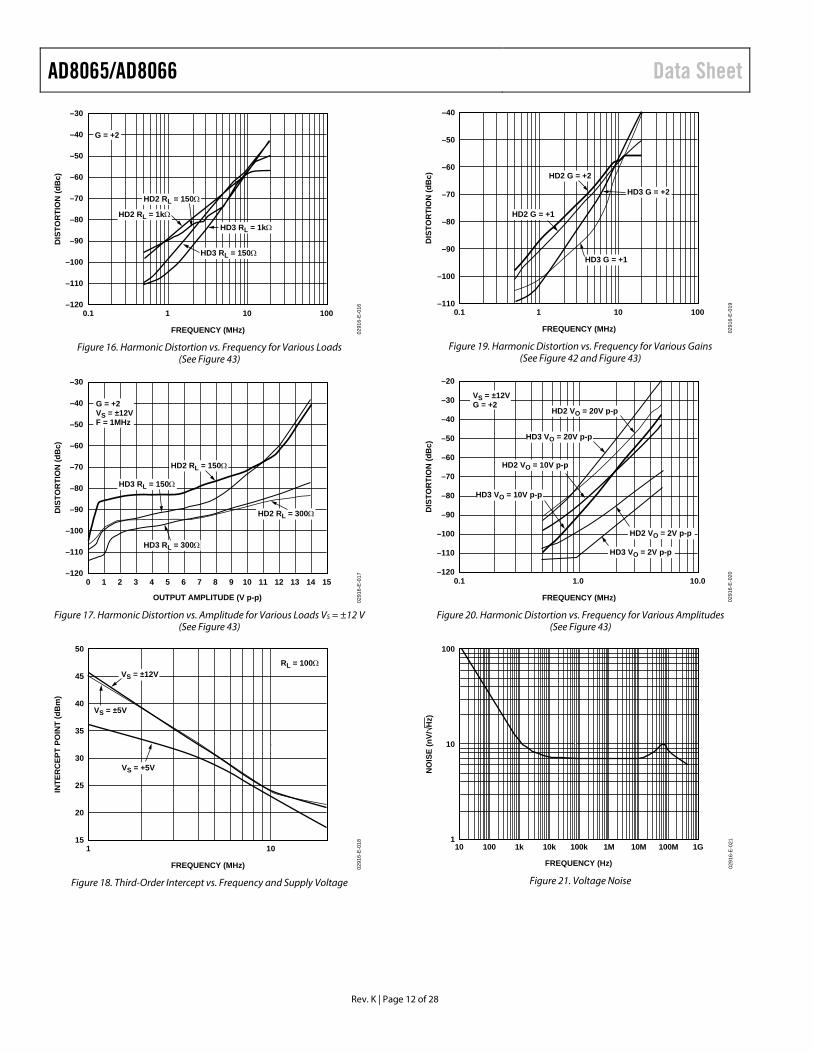
Figure 16. Harmonic Distortion vs. Frequency for Various Loads
(See Figure 43)
–120
–110
–100
–90
–80
–70
–60
–50
–40
–30
DIS
TOR
TIO
N (d
Bc)
0 1 2 3 4 6 105 7 8 9 1211 1413 15
OUTPUT AMPLITUDE (V p-p) 0291
6-E
-017
HD3 RL = 150Ω
HD2 RL = 150Ω
HD3 RL = 300Ω
HD2 RL = 300Ω
G = +2VS = ±12VF = 1MHz
Figure 17. Harmonic Distortion vs. Amplitude for Various Loads VS = ±12 V
(See Figure 43)
15
20
25
30
35
40
45
50
INTE
RC
EPT
POIN
T (d
Bm
)
FREQUENCY (MHz)
1 10
0291
6-E
-018
VS = ±12VRL = 100Ω
VS = ±5V
VS = +5V
Figure 18. Third-Order Intercept vs. Frequency and Supply Voltage
–110
–100
–90
–80
–70
–60
–50
–40
DIS
TOR
TIO
N (d
Bc)
FREQUENCY (MHz)
0.1 101 100
0291
6-E
-019
HD2 G = +2
HD3 G = +2
HD2 G = +1
HD3 G = +1
Figure 19. Harmonic Distortion vs. Frequency for Various Gains
(See Figure 42 and Figure 43)
–120
–110
–100
–90
–80
–70
–60
–50
–40
–30
–20
DIS
TOR
TIO
N (d
Bc)
FREQUENCY (MHz)
0.1 1.0 10.0
0291
6-E
-020
HD2 VO = 20V p-p
HD3 VO = 20V p-p
HD2 VO = 10V p-p
HD3 VO = 10V p-p
HD2 VO = 2V p-p
HD3 VO = 2V p-p
VS = ±12VG = +2
Figure 20. Harmonic Distortion vs. Frequency for Various Amplitudes
(See Figure 43)
NO
ISE
(nV/
Hz)
1
10
100
100k10k100 1k10 1M 10M 100M 1G
FREQUENCY (Hz) 0291
6-E-
021
Figure 21. Voltage Noise

Data Sheet AD8065/AD8066
Rev. K | Page 13 of 28
0291
6-02
2
G = +1
50mV/DIV 25ns/DIV
Figure 22. Small Signal Transient Response 5 V Supply (See Figure 42)
0291
6-02
3G = +1
2V/DIV 50ns/DIV
VS = ±12V
VOUT = 2V p-p
VOUT = 4V p-p
VOUT = 10V p-p
Figure 23. Large Signal Transient Response (See Figure 42)
0291
6-02
4
2.0V/DIV 100ns/DIV
G = –1VS = ±5V
Figure 24. Output Overdrive Recovery (See Figure 44)
0291
6-02
5
G = +1
50mV/DIV 25ns/DIV
CL = 5pF
CL = 20pF
Figure 25. Small Signal Transient Response ±5 V (See Figure 42)
0291
6-02
6
5µsG = +2
2V/DIV 50ns/DIV
VS = ±12VVOUT = 10V p-p
VOUT = 2V p-p
Figure 26. Large Signal Transient Response (See Figure 43)
0291
6-02
7
2.0V/DIV 100ns/DIV
G = +1VS = ±5V
Figure 27. Input Overdrive Recovery (See Figure 42)

AD8065/AD8066 Data Sheet
Rev. K | Page 14 of 28
0291
6-E-
028
t = 0
64µs/DIV2mV/DIV
+0.1%
–0.1%
VIN = 140mV/DIV
VOUT – 2VIN
Figure 28. Long-Term Settling Time (See Figure 49)
–30
–25
–20
–15
–10
–5
0
INPU
T B
IAS
CU
RR
ENT
(pA
)
45 5525 35 65 75 85
TEMPERATURE (°C) 0291
6-E
-029
–Ib
+Ib
Figure 29. Input Bias Current vs. Temperature
–0.3
–0.2
–0.1
0
0.1
0.2
0.3
OFF
SET
VOLT
AG
E (m
V)
–14 –10–12 –8 –6 –4 0 8–2 2 4 6 10 12 14
COMMON-MODE VOLTAGE (V) 0291
6-E-
030
VS = ±12V
VS = ±5V
VS = +5V
Figure 30. Input Offset Voltage vs. Common-Mode Voltage
0291
6-E-
031
+0.1%
2mV/DIV 10ns/DIV
–0.1% t = 0
VOUT – 2VIN
VIN = 500mV/DIV
Figure 31. 0.1% Short-Term Settling Time (See Figure 49)
0291
6-E
-032
0I b
(µA
)
36302418126
–5
–15
–25–30
0
I b (p
A)
–12 8–2–10 0–8 2–6 4–4 6COMMON-MODE VOLTAGE (V)
10 12
42
–Ib
+Ib
–Ib
+Ib
FET
INPU
T ST
AG
EB
JT IN
PUT
STA
GE
–20
–10
510
Figure 32. Input Bias Current vs. Common-Mode Voltage Range
(See the Input and Output Overload Behavior Section)
0291
6-E
-033
INPUT OFFSET VOLTAGE (mV)
35
15
0–2.0 2.0–1.5 –1.0 –0.5 0 0.5 1.0 1.5
30
20
10
5
40
25
N = 299SD = 0.388MEAN = –0.069
Figure 33. Input Offset Voltage
Data Sheet AD8065/AD8066
Rev. K | Page 15 of 28
–100
–90
–80
–70
–60
–50
–40
–30
CM
RR
(dB
)
FREQUENCY (MHz)
0.1 101 100
0291
6-E
-034
VS = ±12V
VS = ±5V
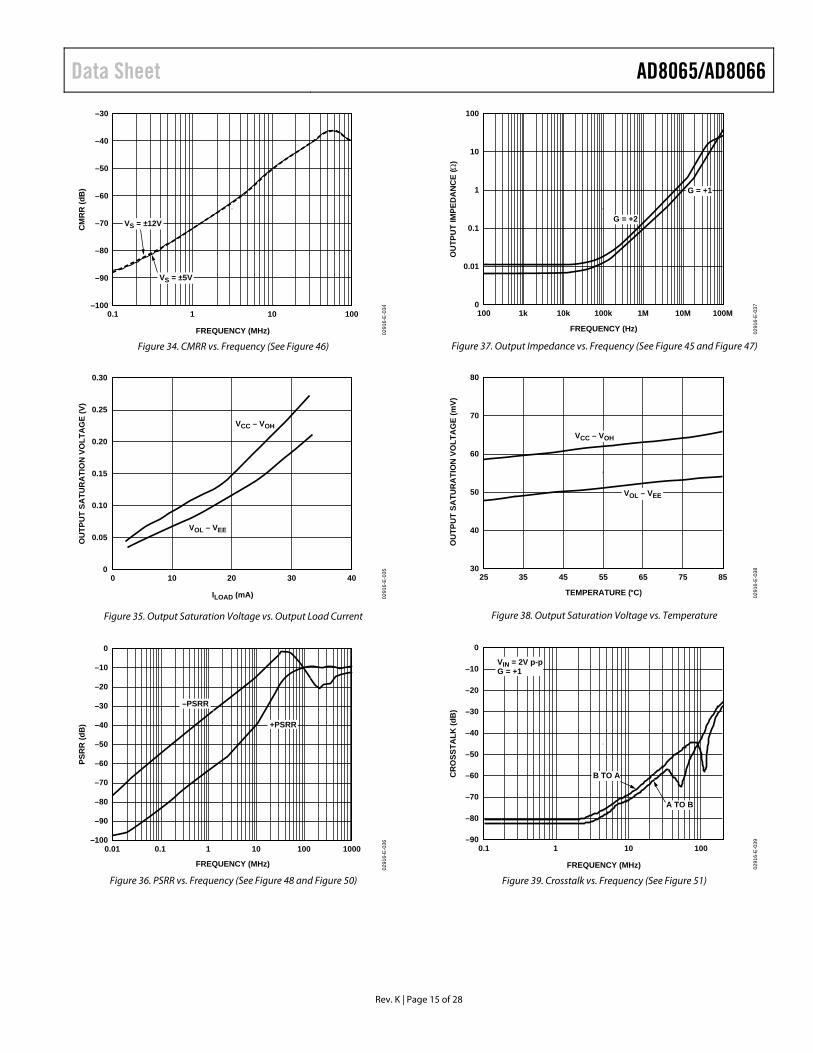
Figure 34. CMRR vs. Frequency (See Figure 46)
0
0.05
0.10
0.15
0.20
0.25
0.30
OU
TPU
T SA
TUR
ATI
ON
VO
LTA
GE
(V)
ILOAD (mA)
100 20 30 40
0291
6-E
-035
VCC – VOH
VOL – VEE
Figure 35. Output Saturation Voltage vs. Output Load Current
–100
–90
–80
–70
–60
–50
–40
–30
–20
–10
0
PSR
R (d
B)
0.01 0.1 1 10 100 1000
FREQUENCY (MHz)
0291
6-E
-036
–PSRR
+PSRR
Figure 36. PSRR vs. Frequency (See Figure 48 and Figure 50)
0
0.01
0.1
1
10
100
OU
TPU
T IM
PED
AN
CE
()
10k 100k100 1k 1M 10M 100M
FREQUENCY (Hz) 0291
6-E-
037
G = +2
G = +1
Figure 37. Output Impedance vs. Frequency (See Figure 45 and Figure 47)
30
40
50
60
70
80
OU
TPU
T SA
TUR
ATI
ON
VO
LTA
GE
(mV)
45 5525 35 65 75 85
TEMPERATURE (°C) 0291
6-E-
038
VCC – VOH
VOL – VEE
Figure 38. Output Saturation Voltage vs. Temperature
–90
–80
–70
–60
–50
–40
–30
–20
–10
0
CR
OSS
TALK
(dB
)
FREQUENCY (MHz)
0.1 101 100
0291
6-E
-039
VIN = 2V p-pG = +1
B TO A
A TO B
Figure 39. Crosstalk vs. Frequency (See Figure 51)
AD8065/AD8066 Data Sheet
Rev. K | Page 16 of 28
6.25
6.30
6.35
6.40
6.45
6.50
6.55
6.60
SUPP
LY C
UR
REN
T (m
A)
0 20–40 –20 40 60 80
TEMPERATURE (°C) 0291
6-E-
040
VS = ±12V
VS = +5V
VS = ±5V
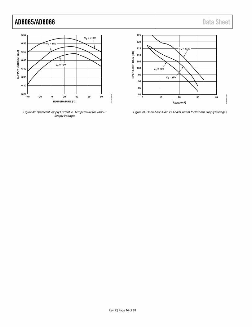
Figure 40. Quiescent Supply Current vs. Temperature for Various Supply Voltages
80
85
90
95
100
105
110
115
120
125
OPE
N-L
OO
P G
AIN
(dB
)
ILOAD (mA)
100 20 30 40
0291
6-E
-041
VS = ±12V
VS = +5V
VS = ±5V
Figure 41. Open-Loop Gain vs. Load Current for Various Supply Voltages
Data Sheet AD8065/AD8066
Rev. K | Page 17 of 28
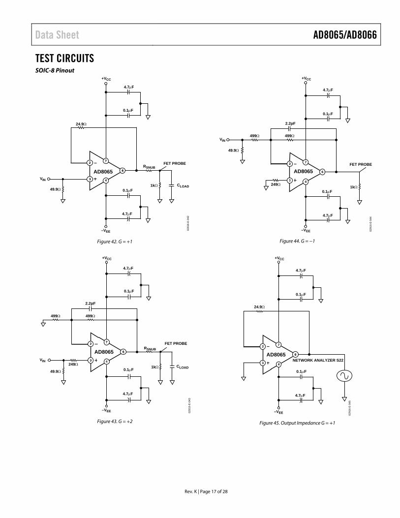
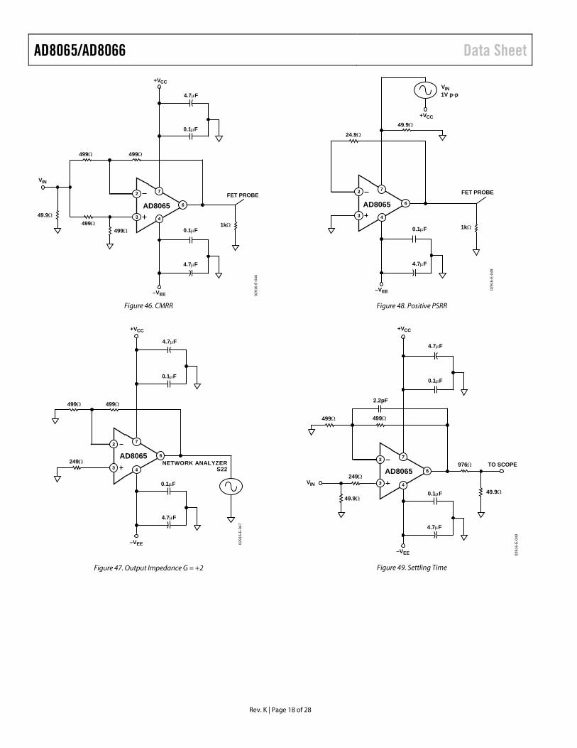
TEST CIRCUITS SOIC-8 Pinout
AD8065
+VCC
VIN
–VEE
4.7µF
0.1µF
24.9Ω
RSNUB
0.1µF
4.7µF
CLOAD
FET PROBE
49.9Ω1kΩ
0291
6-E
-042
Figure 42. G = +1
0291
6-E
-043
AD8065
+VCC
VIN
–VEE
4.7µF
0.1µF
2.2pF
RSNUB
0.1µF
4.7µF
49.9Ω
499Ω 499Ω
249Ω CLOAD
FET PROBE
1kΩ
Figure 43. G = +2
VIN
49.9Ω
AD8065
+VCC
–VEE
4.7µF
0.1µF
2.2pF
0.1µF
4.7µF
499Ω 499Ω
249Ω
FET PROBE
1kΩ
0291
6-E
-044
Figure 44. G = −1
AD8065
+VCC
–VEE
4.7µF
0.1µF
24.9Ω
0.1µF
4.7µF
NETWORK ANALYZER S22
0291
6-E
-045
Figure 45. Output Impedance G = +1
AD8065/AD8066 Data Sheet
Rev. K | Page 18 of 28
VIN
49.9ΩAD8065
+VCC
–VEE
4.7µF
0.1µF
0.1µF
4.7µF
499Ω 499Ω
FET PROBE
1kΩ499Ω499Ω
0291
6-E
-046
Figure 46. CMRR
AD8065
+VCC
–VEE
0.1µF
4.7µF
499Ω 499Ω
249Ω NETWORK ANALYZERS22
4.7µF
0.1µF
0291
6-E
-047
Figure 47. Output Impedance G = +2
AD8065
–VEE
24.9Ω
0.1µF
4.7µF
+VCC
FET PROBE
1kΩ
VIN1V p-p
49.9Ω
0291
6-E
-048
Figure 48. Positive PSRR
AD8065
+VCC
VIN
–VEE
4.7µF
0.1µF
2.2pF
976Ω
0.1µF
4.7µF
499Ω 499Ω
249Ω
TO SCOPE
49.9Ω49.9Ω
0291
6-E
-049
Figure 49. Settling Time
Data Sheet AD8065/AD8066
Rev. K | Page 19 of 28
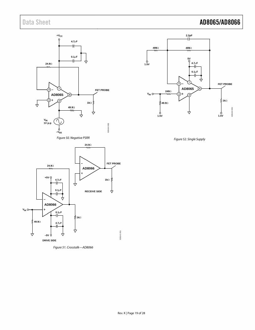
AD8065
+VCC
–VEE
4.7µF
0.1µF
FET PROBE
49.9Ω
24.9Ω
VIN1V p-p
1kΩ
0291
6-E
-050
Figure 50. Negative PSRR
24.9Ω
49.9Ω
24.9Ω
1kΩ
0.1µF
4.7µF
VIN
+5V
–5V
1kΩ
DRIVE SIDE
RECEIVE SIDE
AD8066
AD8066
0.1µF
4.7µF
FET PROBE
0291
6-E
-051
Figure 51. Crosstalk—AD8066
249Ω
0.1µF
VIN
1.5V
1.5V
1.5V
4.7µF
499Ω499Ω
5V
49.9Ω
2.2pF
1kΩ
FET PROBE
AD8065
0291
6-E-
052
Figure 52. Single Supply

AD8065/AD8066 Data Sheet
Rev. K | Page 20 of 28
THEORY OF OPERATION The AD8065/AD8066 are voltage feedback operational amplifiers that combine a laser-trimmed JFET input stage with the Analog Devices eXtra Fast Complementary Bipolar (XFCB) process, resulting in an outstanding combination of precision and speed. The supply voltage range is from 5 V to 24 V. The amplifiers feature a patented rail-to-rail output stage capable of driving within 0.5 V of either power supply while sourcing or sinking up to 30 mA. Also featured is a single-supply input stage that handles common-mode signals from below the negative supply to within 3 V of the positive rail. Operation beyond the JFET input range is possible because of an auxiliary bipolar input stage that functions with input voltages up to the positive supply. The amplifiers operate as if they have a rail-to-rail input and exhibit no phase reversal behavior for common-mode voltages within the power supply.
With voltage noise of 7 nV/√Hz and −88 dBc distortion for 1 MHz, 2 V p-p signals, the AD8065/AD8066 are a great choice for high resolution data acquisition systems. Their low noise, sub-pA input current, precision offset, and high speed make them superb preamps for fast photodiode applications. The speed and output drive capability of the AD8065/AD8066 also make them useful in video applications.
CLOSED-LOOP FREQUENCY RESPONSE The AD8065/AD8066 are classic voltage feedback amplifiers with an open-loop frequency response that can be approximated as the integrator response shown in Figure 53. Basic closed-loop frequency response for inverting and noninverting configurations can be derived from the schematics shown.
NONINVERTING CLOSED-LOOP FREQUENCY RESPONSE Solving for the transfer function
( )( ) GcrossoverGF
FGcrossover
I
O
RfsRRRRf
VV
××π+++×π
=2
2
where fcrossover is the frequency where the amplifier’s open-loop gain equals 0 db
At dc G
GF
I
O
RRR
VV +
=
Closed-loop −3 dB frequency
GF
Gcrossover3dB RR
Rff
+×=−
INVERTING CLOSED-LOOP FREQUENCY RESPONSE
( ) GcrossoverGF
Fcrossover
I
O
RfRRsRf
VV
××π++××π−
=2
2
At dc G
F
I
O
RR
VV
−=
Closed-loop −3 dB frequency
GF
GcrossoverdB RR
Rff
+×=−3
RF
AVO
RG
VIVE
FREQUENCY (MHz)
80
60
0.01 100
OPE
N-L
OO
P G
AIN
(A) (
dB)
0.1 101
40
20
0
fcrossover = 65MHz
A = (2π × fcrossover)/s
RF
VE AVO
RGVI
0291
6-E
-053
Figure 53. Open-Loop Gain vs. Frequency and Basic Connections
Data Sheet AD8065/AD8066
Rev. K | Page 21 of 28
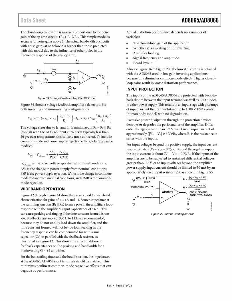
The closed-loop bandwidth is inversely proportional to the noise gain of the op amp circuit, (RF + RG )/RG. This simple model is accurate for noise gains above 2. The actual bandwidth of circuits with noise gains at or below 2 is higher than those predicted with this model due to the influence of other poles in the frequency response of the real op amp.
VO
RF
A
RG
VI
Ib–RS
Ib+
+VOS –
0291
6-E-
054
Figure 54. Voltage Feedback Amplifier DC Errors
Figure 54 shows a voltage feedback amplifier’s dc errors. For both inverting and noninverting configurations
( )
++×−
+×= −+
G
FGOSFb
G
FGSbO R
RRVRI
RRR
RIerrorV
The voltage error due to Ib+ and Ib– is minimized if RS = RF || RG (though with the AD8065 input currents at typically less than 20 pA over temperature, this is likely not a concern). To include common-mode and power supply rejection effects, total VOS can be modeled
CMRV
PSRV
VV CMSnomOSOS
ΔΔ++=
nomOSV is the offset voltage specified at nominal conditions, ΔVS is the change in power supply from nominal conditions, PSR is the power supply rejection, ΔVCM is the change in common-mode voltage from nominal conditions, and CMR is the common-mode rejection.
WIDEBAND OPERATION Figure 42 through Figure 44 show the circuits used for wideband characterization for gains of +1, +2, and −1. Source impedance at the summing junction (RF || RG) forms a pole in the amplifier’s loop response with the amplifier’s input capacitance of 6.6 pF. This can cause peaking and ringing if the time constant formed is too low. Feedback resistances of 300 Ω to 1 kΩ are recommended, because they do not unduly load down the amplifier, and the time constant formed will not be too low. Peaking in the frequency response can be compensated for with a small capacitor (CF) in parallel with the feedback resistor, as illustrated in Figure 12. This shows the effect of different feedback capacitances on the peaking and bandwidth for a noninverting G = +2 amplifier.
For the best settling times and the best distortion, the impedances at the AD8065/AD8066 input terminals should be matched. This minimizes nonlinear common-mode capacitive effects that can degrade ac performance.
Actual distortion performance depends on a number of variables:
• The closed-loop gain of the application • Whether it is inverting or noninverting • Amplifier loading • Signal frequency and amplitude • Board layout
Also see Figure 16 to Figure 20. The lowest distortion is obtained with the AD8065 used in low gain inverting applications, because this eliminates common-mode effects. Higher closed-loop gains result in worse distortion performance.
INPUT PROTECTION The inputs of the AD8065/AD8066 are protected with back-to-back diodes between the input terminals as well as ESD diodes to either power supply. This results in an input stage with picoamps of input current that can withstand up to 1500 V ESD events (human body model) with no degradation.
Excessive power dissipation through the protection devices destroys or degrades the performance of the amplifier. Differ-ential voltages greater than 0.7 V result in an input current of approximately (|V+ − V−| 0.7 V)/RI, where RI is the resistance in series with the inputs.
For input voltages beyond the positive supply, the input current is approximately (VI − VCC − 0.7)/RI. Beyond the negative supply, the input current is about (VI − VEE + 0.7)/RI. If the inputs of the amplifier are to be subjected to sustained differential voltages greater than 0.7 V, or to input voltages beyond the amplifier power supply, input current should be limited to 30 mA by an appropriately sized input resistor (RI), as shown in Figure 55.
RIVI VO
AD8065
RI >(| V+– V– | – 0.7V)
30mA
FOR LARGE | V+ – V– |
RI >(VI – VEE – 0.7V)
30mA
RI >(VI – VEE + 0.7V)
30mAFOR VI BEYONDSUPPLY VOLTAGES
0291
6-E-
055
Figure 55. Current-Limiting Resistor
AD8065/AD8066 Data Sheet
Rev. K | Page 22 of 28
THERMAL CONSIDERATIONS With 24 V power supplies and 6.5 mA quiescent current, the AD8065 dissipates 156 mW with no load. The AD8066 dissipates 312 mW. This can lead to noticeable thermal effects, especially in the small SOT-23-5 (thermal resistance of 160°C/W). VOS temperature drift is trimmed to guarantee a maximum drift of 17 μV/°C, so it can change up to 0.425 mV due to warm-up effects for an AD8065/AD8066 in a SOT-23-5 package on 24 V.
Ib increases by a factor of 1.7 for every 10°C rise in temperature. Ib is close to five times higher at 24 V supplies as opposed to a single 5 V supply.
Heavy loads increase power dissipation and raise the chip junction temperature as described in the Maximum Power Dissipation section. Care should be taken not to exceed the rated power dissipation of the package.
INPUT AND OUTPUT OVERLOAD BEHAVIOR A simplified schematic of the AD8065/AD8066 input stage is shown in Figure 56. This shows the cascoded N-channel JFET input pair, the ESD and other protection diodes, and the auxiliary NPN input stage that eliminates any phase inversion behavior. When the common-mode input voltage to the amplifier is driven to within approximately 3 V of the positive power supply, the input JFET’s bias current turns off and the bias of the NPN pair turns on, taking over control of the amplifier. The NPN differential pair now sets the amplifier’s offset, and the input bias current is now in the range of several tens of microamps. This behavior is shown in Figure 32. Normal operation resumes when the common-mode voltage goes below the 3 V from the positive supply threshold.
The output transistors of the rail-to-rail output stage have circuitry to limit the extent of their saturation when the output is overdriven. This helps output recovery time. Output recovery from a 0.5 V output overdrive on a ±5 V supply is shown in Figure 24.
VTHRESHOLD
VBIAS
S
VP
TO REST OF AMP
VCC
S
VN
R1
Q2 Q5
Q3
Q1 Q6
Q7
Q4
R5
D1 R6
R3
R4
R2 R8
R7
D2D3 D4
–VEE
IT1 IT2
0291
6-E-
056
Figure 56. Simplified Input Stage
Data Sheet AD8065/AD8066
Rev. K | Page 23 of 28
LAYOUT, GROUNDING, AND BYPASSING CONSIDERATIONS POWER SUPPLY BYPASSING Power supply pins are actually inputs and care must be taken so that a noise-free stable dc voltage is applied. The purpose of bypass capacitors is to create low impedances from the supply to ground at all frequencies, thereby shunting or filtering most of the noise.
Decoupling schemes are designed to minimize the bypassing impedance at all frequencies with a parallel combination of capacitors. 0.1 µF (X7R or NPO) chip capacitors are critical and should be as close as possible to the amplifier package. The 4.7 µF tantalum capacitor is less critical for high frequency bypassing, and, in most cases, only one is needed per board at the supply inputs.
GROUNDING A ground plane layer is important in densely packed PC boards to spread the current minimizing parasitic inductances. However, an understanding of where the current flows in a circuit is critical to implementing effective high speed circuit design. The length of the current path is directly proportional to the magnitude of parasitic inductances and, therefore, the high frequency impedance of the path. High speed currents in an inductive ground return create unwanted voltage noise.
The length of the high frequency bypass capacitor leads is most critical. A parasitic inductance in the bypass grounding works against the low impedance created by the bypass capacitor. Place the ground leads of the bypass capacitors at the same physical location. Because load currents flow from the supplies as well, the ground for the load impedance should be at the same physical location as the bypass capacitor grounds. For the larger value capacitors, which are effective at lower frequencies, the current return path distance is less critical.
LEAKAGE CURRENTS Poor PC board layout, contaminants, and the board insulator material can create leakage currents that are much larger than the input bias current of the AD8065/AD8066. Any voltage differential between the inputs and nearby runs sets up leakage currents through the PC board insulator, for example, 1 V/100 GΩ = 10 pA. Similarly, any contaminants on the board can create significant leakage (skin oils are a common problem). To reduce leakage significantly, put a guard ring (shield) around the inputs and input leads that are driven to the same voltage potential as the inputs. This way there is no voltage potential between the
inputs and surrounding area to set up any leakage currents. For the guard ring to be completely effective, it must be driven by a relatively low impedance source and should completely surround the input leads on all sides, above and below, using a multilayer board.
Another effect that can cause leakage currents is the charge absorption of the insulator material itself. Minimizing the amount of material between the input leads and the guard ring helps to reduce the absorption. Also, low absorption materials, such as Teflon® or ceramic, could be necessary in some instances.
INPUT CAPACITANCE Along with bypassing and ground, high speed amplifiers can be sensitive to parasitic capacitance between the inputs and ground. A few pF of capacitance reduces the input impedance at high frequencies, in turn increasing the amplifier’s gain, causing peaking of the frequency response or even oscillations, if severe enough. It is recommended that the external passive components connected to the input pins be placed as close as possible to the inputs to avoid parasitic capacitance. The ground and power planes must be kept at a small distance from the input pins on all layers of the board.
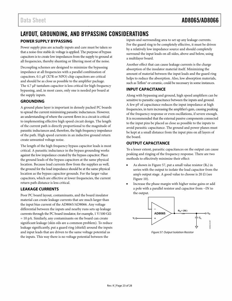
OUTPUT CAPACITANCE To a lesser extent, parasitic capacitances on the output can cause peaking and ringing of the frequency response. There are two methods to effectively minimize their effect:
• As shown in Figure 57, put a small value resistor (RS) in series with the output to isolate the load capacitor from the amp’s output stage. A good value to choose is 20 Ω (see Figure 10).
• Increase the phase margin with higher noise gains or add a pole with a parallel resistor and capacitor from −IN to the output.
RS = 20Ω
VI
AD8065CL
VO
0291
6-E-
057
Figure 57. Output Isolation Resistor
AD8065/AD8066 Data Sheet
Rev. K | Page 24 of 28
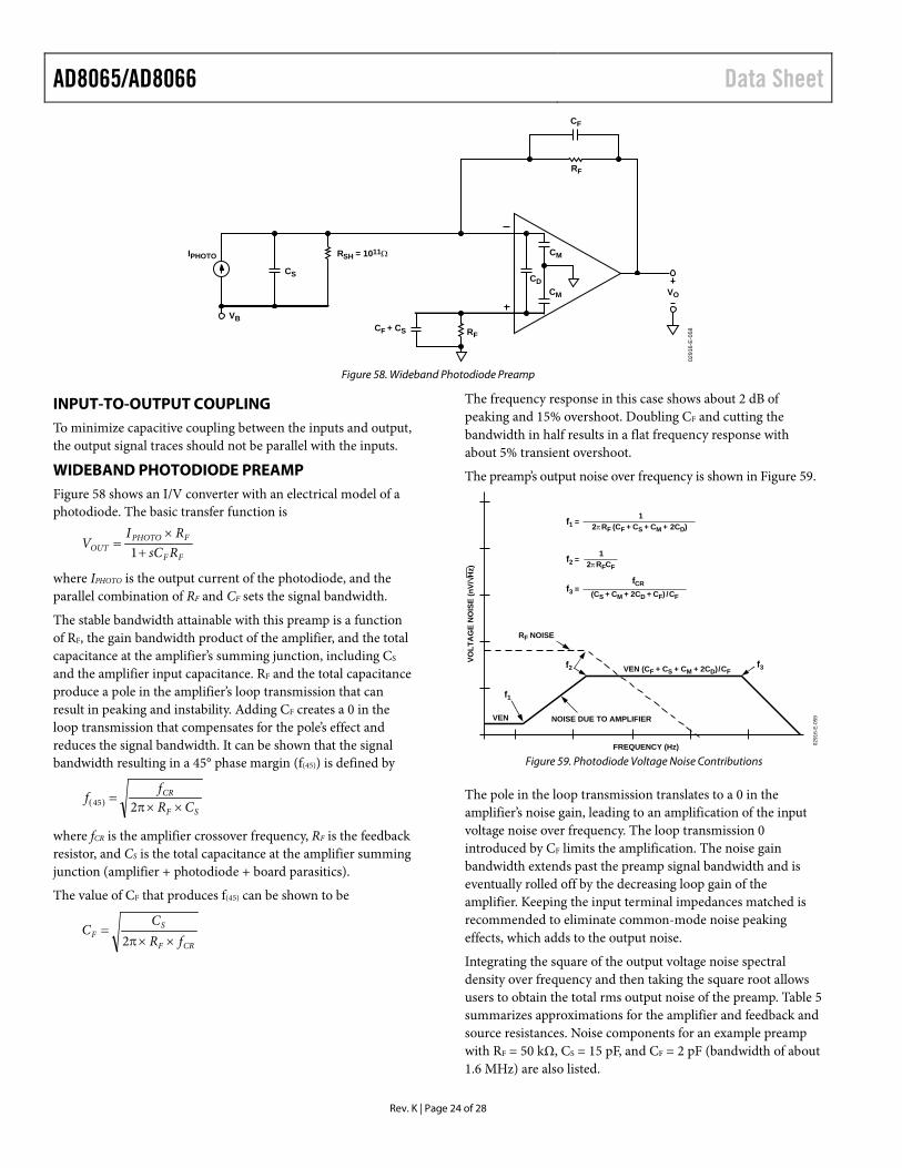
RSH = 1011Ω
VO
RF
CF
CM
RF
CM
CD
CF + CS
CS
VB
IPHOTO
0291
6-E-
058
Figure 58. Wideband Photodiode Preamp
INPUT-TO-OUTPUT COUPLING To minimize capacitive coupling between the inputs and output, the output signal traces should not be parallel with the inputs.
WIDEBAND PHOTODIODE PREAMP Figure 58 shows an I/V converter with an electrical model of a photodiode. The basic transfer function is
FF
FPHOTOOUT RsC
RIV
+×
=1
where IPHOTO is the output current of the photodiode, and the parallel combination of RF and CF sets the signal bandwidth.
The stable bandwidth attainable with this preamp is a function of RF, the gain bandwidth product of the amplifier, and the total capacitance at the amplifier’s summing junction, including CS and the amplifier input capacitance. RF and the total capacitance produce a pole in the amplifier’s loop transmission that can result in peaking and instability. Adding CF creates a 0 in the loop transmission that compensates for the pole’s effect and reduces the signal bandwidth. It can be shown that the signal bandwidth resulting in a 45° phase margin (f(45)) is defined by
( )SF
CR
CRf
f××π
=245
where fCR is the amplifier crossover frequency, RF is the feedback resistor, and CS is the total capacitance at the amplifier summing junction (amplifier + photodiode + board parasitics).
The value of CF that produces f(45) can be shown to be
CRF
SF fR
CC
××π=
2
The frequency response in this case shows about 2 dB of peaking and 15% overshoot. Doubling CF and cutting the bandwidth in half results in a flat frequency response with about 5% transient overshoot.
The preamp’s output noise over frequency is shown in Figure 59.
FREQUENCY (Hz)
VOLT
AG
E N
OIS
E (n
V/H
z) 2πRFCF
2πRF (CF + CS + CM + 2CD)
(CS + CM + 2CD + CF) /CF
RF NOISE
VEN (CF + CS + CM + 2CD)/CFf3f2
f3 =
VEN
f1
f2 =
f1 =1
1
fCR
NOISE DUE TO AMPLIFIER
0291
6-E
-059
Figure 59. Photodiode Voltage Noise Contributions
The pole in the loop transmission translates to a 0 in the amplifier’s noise gain, leading to an amplification of the input voltage noise over frequency. The loop transmission 0 introduced by CF limits the amplification. The noise gain bandwidth extends past the preamp signal bandwidth and is eventually rolled off by the decreasing loop gain of the amplifier. Keeping the input terminal impedances matched is recommended to eliminate common-mode noise peaking effects, which adds to the output noise.
Integrating the square of the output voltage noise spectral density over frequency and then taking the square root allows users to obtain the total rms output noise of the preamp. Table 5 summarizes approximations for the amplifier and feedback and source resistances. Noise components for an example preamp with RF = 50 kΩ, CS = 15 pF, and CF = 2 pF (bandwidth of about 1.6 MHz) are also listed.
Data Sheet AD8065/AD8066
Rev. K | Page 25 of 28
Table 5. RMS Noise Contributions of Photodiode Preamp Contributor Expression RMS Noise with RF = 50 kΩ, CS = 15 pF, CF = 2 pF RF (×2) 57142 .fRkT 2F ×××× 64.5 µV
Amp to f1 1fVEN × 2.4 µV
Amp (f2 – f1) 12
F
DFMS ffC
CCCCVEN −×
+++×
2
31 µV
Amp to (past f2) 57.1
2××
+++× 3
F
FDMS fC
CCCCVEN
260 µV
270 µV (Total)
VCC
VEE
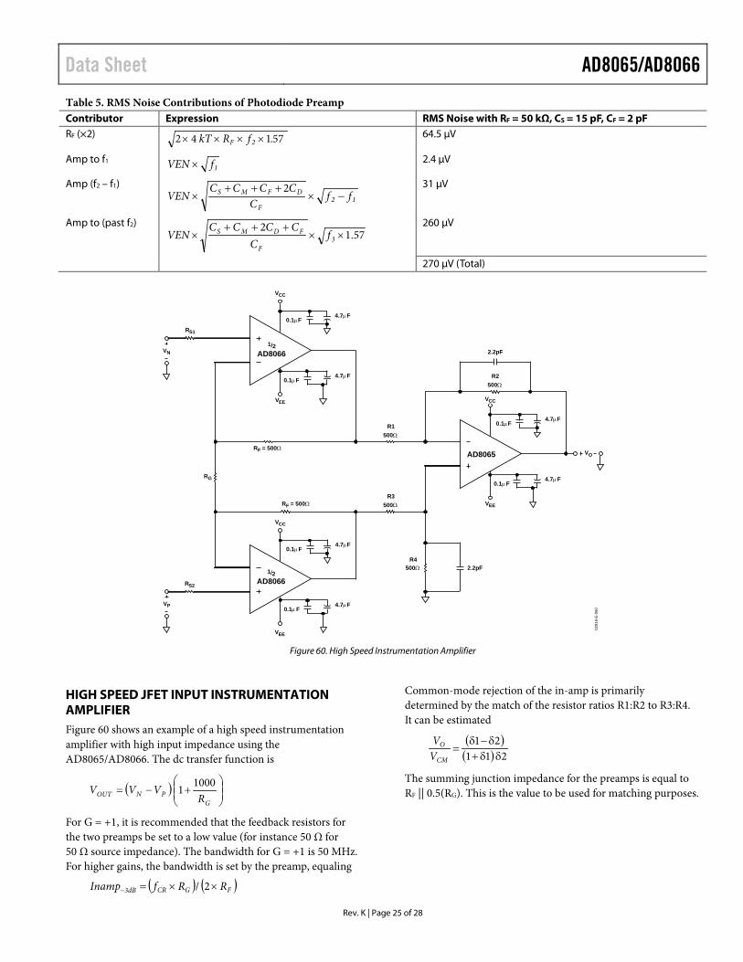
1/2AD8066
4.7µF0.1µF
RS1
4.7µF0.1µF
VN 2.2pF
500ΩR2
VP
1/2AD8066
4.7µF0.1µF
4.7µF0.1µF
AD8065
4.7µF0.1µF
4.7µF0.1µF
VO
RG
VCC
VEE
VCC
VEE
500ΩR4
RS2
500ΩR1
500ΩR3
RF = 500Ω
2.2pF
RF = 500Ω
0291
6-E
-060
Figure 60. High Speed Instrumentation Amplifier
HIGH SPEED JFET INPUT INSTRUMENTATION AMPLIFIER Figure 60 shows an example of a high speed instrumentation amplifier with high input impedance using the AD8065/AD8066. The dc transfer function is
( )
+−=
GPNOUT R
VVV 10001
For G = +1, it is recommended that the feedback resistors for the two preamps be set to a low value (for instance 50 Ω for 50 Ω source impedance). The bandwidth for G = +1 is 50 MHz. For higher gains, the bandwidth is set by the preamp, equaling
( ) ( )FGCR3dB RRfInamp ××=− 2/
Common-mode rejection of the in-amp is primarily determined by the match of the resistor ratios R1:R2 to R3:R4. It can be estimated
( )( ) 211
21δδ+
δ−δ=
CM
O
VV
The summing junction impedance for the preamps is equal to RF || 0.5(RG). This is the value to be used for matching purposes.
AD8065/AD8066 Data Sheet
Rev. K | Page 26 of 28
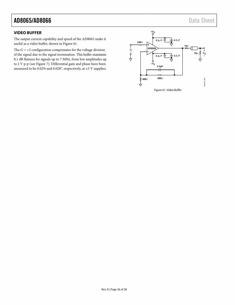
VIDEO BUFFER The output current capability and speed of the AD8065 make it useful as a video buffer, shown in Figure 61.
The G = +2 configuration compensates for the voltage division of the signal due to the signal termination. This buffer maintains 0.1 dB flatness for signals up to 7 MHz, from low amplitudes up to 2 V p-p (see Figure 7). Differential gain and phase have been measured to be 0.02% and 0.028°, respectively, at ±5 V supplies.
+VS
–VS
4.7µF0.1µF
2.2pF
499Ω
249Ω75Ω
499Ω
VIAD8065
4.7µF0.1µF75Ω VO
+
– +
–
0291
6-E
-061
Figure 61. Video Buffer

Data Sheet AD8065/AD8066
Rev. K | Page 27 of 28
OUTLINE DIMENSIONS
CONTROLLING DIMENSIONS ARE IN MILLIMETERS; INCH DIMENSIONS(IN PARENTHESES) ARE ROUNDED-OFF MILLIMETER EQUIVALENTS FORREFERENCE ONLY AND ARE NOT APPROPRIATE FOR USE IN DESIGN.
COMPLIANT TO JEDEC STANDARDS MS-012-AA
0124
07-A
0.25 (0.0098)0.17 (0.0067)
1.27 (0.0500)0.40 (0.0157)
0.50 (0.0196)0.25 (0.0099) 45°
8°0°
1.75 (0.0688)1.35 (0.0532)
SEATINGPLANE
0.25 (0.0098)0.10 (0.0040)
41
8 5
5.00 (0.1968)4.80 (0.1890)
4.00 (0.1574)3.80 (0.1497)
1.27 (0.0500)BSC
6.20 (0.2441)5.80 (0.2284)
0.51 (0.0201)0.31 (0.0122)
COPLANARITY0.10
Figure 62. 8-Lead Standard Small Outline Package [SOIC_N]
Narrow Body (R-8) Dimensions shown in millimeters and (inches)
COMPLIANT TO JEDEC STANDARDS MO-178-AA
10°5°0°
SEATINGPLANE
1.90BSC
0.95 BSC
0.60BSC
5
1 2 3
4
3.002.902.80
3.002.802.60
1.701.601.50
1.301.150.90
0.15 MAX0.05 MIN
1.45 MAX0.95 MIN
0.20 MAX0.08 MIN
0.50 MAX0.35 MIN
0.550.450.35
11-0
1-20
10-A
Figure 63. 5-Lead Small Outline Transistor Package [SOT-23]
(RJ-5) Dimensions shown in millimeters
COMPLIANT TO JEDEC STANDARDS MO-187-AA
6°0°
0.800.550.40
4
8
1
5
0.65 BSC
0.400.25
1.10 MAX
3.203.002.80
COPLANARITY0.10
0.230.09
3.203.002.80
5.154.904.65
PIN 1IDENTIFIER
15° MAX0.950.850.75
0.150.05
10-0
7-20
09-B
Figure 64. 8-Lead Mini Small Outline Package [MSOP]
(RM-8) Dimensions shown in millimeters

AD8065/AD8066 Data Sheet
Rev. K | Page 28 of 28
ORDERING GUIDE Model1, 2 Temperature Range Package Description Package Option Branding AD8065AR −40°C to +85°C 8-Lead SOIC_N R-8 AD8065ARZ −40°C to +85°C 8-Lead SOIC_N R-8 AD8065ARZ-REEL −40°C to +85°C 8-Lead SOIC_N R-8 AD8065ARZ-REEL7 −40°C to +85°C 8-Lead SOIC_N R-8 AD8065ART-R2 −40°C to +85°C 5-Lead SOT-23 RJ-5 HRA AD8065ART-REEL7 −40°C to +85°C 5-Lead SOT-23 RJ-5 HRA AD8065ARTZ-R2 −40°C to +85°C 5-Lead SOT-23 RJ-5 HRA # AD8065ARTZ-REEL −40°C to +85°C 5-Lead SOT-23 RJ-5 HRA # AD8065ARTZ-REEL7 −40°C to +85°C 5-Lead SOT-23 RJ-5 HRA # AD8065WARTZ-REEL7 −40°C to +105°C 5-Lead SOT-23 RJ-5 H2F# AD8066ARZ −40°C to +85°C 8-Lead SOIC_N R-8 AD8066ARZ-RL −40°C to +85°C 8-Lead SOIC_N R-8 AD8066ARZ-R7 −40°C to +85°C 8-Lead SOIC_N R-8 AD8066ARM −40°C to +85°C 8-Lead MSOP RM-8 H1B AD8066ARMZ −40°C to +85°C 8-Lead MSOP RM-8 H7C AD8066ARMZ-REEL7 −40°C to +85°C 8-Lead MSOP RM-8 H7C 1 Z = RoHS Compliant Part, # denotes RoHS compliant product may be top or bottom marked. 2 W = Qualified for Automotive Applications.
AUTOMOTIVE PRODUCTS The AD8065W model is available with controlled manufacturing to support the quality and reliability requirements of automotive applications. Note that these automotive models may have specifications that differ from the commercial models; therefore, designers should review the Specifications section of this data sheet carefully. Only the automotive grade products shown are available for use in automotive applications. Contact your local Analog Devices account representative for specific product ordering information and to obtain the specific Automotive Reliability reports for these models.
©2002–2016 Analog Devices, Inc. All rights reserved. Trademarks and registered trademarks are the property of their respective owners. D02916-0-8/16(K)