Embed Size (px)
Citation preview
Information furnished by Analog Devices is be lieved to be accurate and reliable. However, no responsibility is assumed by Analog Devices for its use, nor for any infringements of patents or other rights of third parties that may result from its use. No license is granted by implication or oth-erwise under any patent or patent rights of Analog Devices. Trademarks and registered trademarks are the property of their respective owners.
One Technology Way, P.O. Box 9106, Norwood, MA 02062-9106, U.S.A.Tel: 781/329-4700 www.analog.comFax: 781/326-8703 © 2003 Analog Devices, Inc. All rights reserved.
AD8065/AD8066*
High Performance, 145 MHz FastFET ™ Op Amps
*Protected by U.S. Patent No. 6,262,633
FEATURESFET Input Amplifi er1 pA Input Bias CurrentLow Cost High Speed 145 MHz, −3 dB Bandwidth (G = +1)180 V/s Slew Rate (G = +2)Low Noise 7 nV/HzHzHzHz (f = 10 kHz)Hz (f = 10 kHz)Hz 0.6 fA/HzHzHzHz (f = 10 kHz)Hz (f = 10 kHz)HzWide Supply Voltage Range 5 V to 24 V Single-Supply and Rail-to-Rail OutputLow Offset Voltage 1.5 mV MaxHigh Common-Mode Rejection Ratio −100 dBExcellent Distortion Specifi cationsSFDR −88 dB @ 1 MHzLow Power 6.4 mA/Amplifi er Typical Supply CurrentNo Phase ReversalSmall Packaging SOIC-8, SOT-23-5, and MSOP
APPLICATIONSInstrumentationPhotodiode PreampFiltersA/D DriverLevel ShiftingBuffering
GENERAL DESCRIPTIONThe AD8065/AD8066 FastFET amplifi ers are voltage feedback amplifi ers with FET inputs offering very high performance and ease of use. The AD8065 is a single amplifi er and the AD8066 is a dual amplifi er. The FastFET amplifi ers in ADI’s proprietary XFCB process allow exceptionally low noise operation (7.0 nV/HzHzHzHzand 0.6 fA/HzHzHzHz ) as well as very high input impedance.
With a wide supply voltage range from 5 V to 24 V, the ability to operate on single supplies, and a bandwidth of 145 MHz, the AD8065/AD8066 are designed to work in a variety of applications. For added versatility, the amplifi ers also contain rail-to-rail outputs.
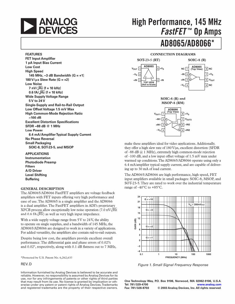
Despite being low cost, the amplifi ers provide excellent overall performance. The differential gain and phase errors of 0.02% and 0.02°, respectively, along with 0.1 dB fl atness out to 7 MHz,
make these amplifi ers ideal for video applications. Additionally, they offer a high slew rate of 180 V/µs, excellent distortion (SFDR of –88 dB @ 1 MHz), extremely high common-mode rejection of –100 dB, and a low input offset voltage of 1.5 mV max under warmed up conditions. The AD8065/AD8066 operate using only a 6.4 mA/amplifi er typical supply current, and are capable of deliver-ing up to 30 mA of load current.
The AD8065/AD8066 are high performance, high speed, FET input amplifi ers available in small packages: SOIC-8, MSOP, and SOT-23-5. They are rated to work over the industrial temperature range of –40°C to +85°C.
FREQUENCY (MHz)
24
0.1 1000
GA
IN (
dB
)
9
1 10 100
21
18
15
12
6
3
0
–3
–6
G = +10
G = +5
G = +2
G = +1
VO = 200mVp-p
Figure 1. Small Signal Frequency Response
CONNECTION DIAGRAMS
SOT-23-5 (RT)
1
2
3TOP VIEW
(Not to Scale)
5
4
VOUTAD8065
–VS
+IN
+VS
–IN
1NC
–IN
+IN
–VS
NC
+VS
VOUT
NC
8
2 7
3 6
4 5
AD8065(Top View)
SOIC-8 (R)
SOIC-8 (R) and MSOP-8 (RM)
1VOUT1
–IN1
+IN1
–VS
+VS
VOUT2
–IN2
+IN2
8
2 7
3 6
4 5
AD8066(Top View)
REV. D

–2–
AD8065/AD8066–SPECIFICATIONSParameter Conditions Min Typ Max Unit
DYNAMIC PERFORMANCE –3 dB Bandwidth G = +1, VO = 0.2 V p-p (AD8065) 100 145 MHz G = +1, VO = 0.2 V p-p (AD8066) 100 120 MHz G = +2, VO = 0.2 V p-p 50 MHz G = +2, VO = 2 V p-p 42 MHz Bandwidth for 0.1 dB Flatness G = +2, VO = 0.2 V p-p 7 MHz Input Overdrive Recovery Time G = +1, –5.5 V to +5.5 V 175 ns Output Recovery Time G = –1, –5.5 V to +5.5 V 170 ns Slew Rate G = +2, VO = 4 V Step 130 180 V/µs Settling Time to 0.1% G = +2, VO = 2 V Step 55 ns G = +2, VO = 8 V Step 205 ns
NOISE/HARMONIC PERFORMANCE SFDR SFDR SFDR fCfCf = 1 MHz, G = +2, VO = 2 V p-p –88 dBc fCfCf = 5 MHz, G = +2, VO = 2 V p-p –67 dBc fCfCf = 1 MHz, G = +2, VO = 8 V p-p –73 dBc Third-Order Intercept fCfCf = 10 MHz, RL = 10 MHz, RL = 10 MHz, R = 100 L = 100 L 24 dBm Input Voltage Noise f = 10 kHz 7 nV/HzHzHz Input Current Noise f = 10 kHz 0.6 fA/
HzHzHz
Differential Gain Error NTSC, G = +2, RLNTSC, G = +2, RLNTSC, G = +2, R = 150 L = 150 L 0.02 % Differential Phase Error NTSC, G = +2, RLNTSC, G = +2, RLNTSC, G = +2, R = 150 L = 150 L 0.02 Degree
DC PERFORMANCE Input Offset Voltage VCM = 0 V, SOIC Package 0.4 1.5 mV Input Offset Voltage Drift 1 17 µV/ºC Input Bias Current SOIC Package 2 6 pA TMIN to TMAX 25 pA Input Offset Current 1 10 pA TMIN to TMAX 1 pA Open-Loop Gain VO = 3 V, RL3 V, RL3 V, R = 1 kL = 1 kL 100 113 dB
INPUT CHARACTERISTICS Common-Mode Input Impedance 1000 2.1 G pF Differential Input Impedance 1000 4.5 G pF Input Common-Mode Voltage Range FET Input Range –5 to +1.7 –5.0 to +2.4 V Usable Range See Theory of Operation section –5.0 to +5.0 V Common-Mode Rejection Ratio VCM = –1 V to +1 V –85 –100 dB VCM = –1 V to +1 V (SOT-23) –82 –91 dB
OUTPUT CHARACTERISTICS Output Voltage Swing RLRLR = 1 kL = 1 kL –4.88 to +4.90 –4.94 to +4.95 V RLRLR = 150 L = 150 L –4.8 to +4.7 V Output Current VO = 9 V p-p, SFDR ≥ –60 dBc, f = 500 kHz 35 mA Short-Circuit Current 90 mA Capacitive Load Drive 30% Overshoot G = +1 20 pF
POWER SUPPLY Operating Range 5 24 V Quiescent Current per Amplifi er 6.4 7.2 mA Power Supply Rejection Ratio ±PSRR –85 –100 dB
Specifi cations subject to change without notice.
(@ TA = 25C, VS = 5 V, RL = 1 k, unless otherwise noted.)
REV. D

AD8065/AD8066
–3–
Parameter Conditions Min Typ Max Unit
DYNAMIC PERFORMANCE –3 dB Bandwidth G = +1, VO = 0.2 V p-p (AD8065) 100 145 MHz G = +1, VO = 0.2 V p-p (AD8066) 100 115 MHz G = +2, VO = 0.2 V p-p 50 MHz G = +2, VO = 2 V p-p 40 MHz Bandwidth for 0.1 dB Flatness G = +2, VO = 0.2 V p-p 7 MHz Input Overdrive Recovery G = +1, –12.5 V to +12.5 V 175 ns Output Overdrive Recovery G = –1, –12.5 V to +12.5 V 170 ns Slew Rate G = +2, VO = 4 V Step 130 180 V/µs Settling Time to 0.1% G = +2, VO = 2 V Step 55 ns G = +2, VO = 10 V Step 250 nsNOISE/HARMONIC PERFORMANCE SFDR SFDR SFDR fCfCf = 1 MHz, G = +2, VO = 2 V p-p –100 dBc fCfCf = 5 MHz, G = +2, VO = 2 V p-p –67 dBc fCfCf = 1 MHz, G = +2, VO = 10 V p-p –85 dBc Third-Order Intercept fCfCf = 10 MHz, RL = 10 MHz, RL = 10 MHz, R = 100 L = 100 L 24 dBm Input Voltage Noise f = 10 kHz 7 nV/HzHzHz Input Current Noise f = 10 kHz 1 fA/
HzHzHz
Differential Gain Error NTSC, G = +2, RLNTSC, G = +2, RLNTSC, G = +2, R = 150 L = 150 L 0.04 % Differential Phase Error NTSC, G = +2, RLNTSC, G = +2, RLNTSC, G = +2, R = 150 L = 150 L 0.03 DegreeDC PERFORMANCE Input Offset Voltage VCM = 0 V, SOIC Package 0.4 1.5 mV Input Offset Voltage Drift 1 17 µV/ºC Input Bias Current SOIC Package 3 7 pA TMIN to TMAX 25 pA Input Offset Current 2 10 pA TMIN to TMAX 2 pA Open-Loop Gain VO = ±10 V, RL = ±10 V, RL = ±10 V, R = 1 kL = 1 kL 103 114 dBINPUT CHARACTERISTICS Common-Mode Input Impedance 1000 2.1 G pF Differential Input Impedance 1000 4.5 G pF Input Common-Mode Voltage Range FET Input Range –12 to +8.5 –12.0 to +9.5 V Usable Range See Theory of Operation section –12.0 to +12.0 V Common-Mode Rejection Ratio VCM = –1 V to +1 V –85 –100 dB VCM = –1 V to +1 V (SOT-23) –82 –91 dBOUTPUT CHARACTERISTICS Output Voltage Swing RLRLR = 1 kL = 1 kL –11.8 to +11.8 –11.9 to +11.9 V RLRLR = 350 L = 350 L –11.25 to +11.5 V Output Current VO = 22 V p-p, SFDR ≥ –60 dBc, f = 500 kHz 30 mA Short-Circuit Current 120 mA Capacitive Load Drive 30% Overshoot G = +1 25 pFPOWER SUPPLY Operating Range 5 24 V Quiescent Current per Amplifi er 6.6 7.4 mA Power Supply Rejection Ratio ±PSRR –84 –93 dB
Specifi cations subject to change without notice.
(@ TA = 25C, VS = 12 V, RL = 1 k, unless otherwise noted.)SPECIFICATIONS
REV. D
–4–
AD8065/AD8066Parameter Conditions Min Typ Max Unit
DYNAMIC PERFORMANCE –3 dB Bandwidth G = +1, VO = 0.2 V p-p (AD8065) 125 155 MHz G = +1, VO = 0.2 V p-p (AD8066) 110 130 MHz G = +2, VO = 0.2 V p-p 50 MHz G = +2, VO = 2 V p-p 43 MHz Bandwidth for 0.1 dB Flatness G = +2, VO = 0.2 V p-p 6 MHz Input Overdrive Recovery Time G = +1, –0.5 V to +5.5 V 175 ns Output Recovery Time G = –1, –0.5 V to +5.5 V 170 ns Slew Rate G = +2, VO = 2 V Step 105 160 V/µs Settling Time to 0.1% G = +2, VO = 2 V Step 60 ns
NOISE/HARMONIC PERFORMANCE SFDR SFDR SFDR fCfCf = 1 MHz, G = +2, VO = 2 V p-p –65 dBc fCfCf = 5 MHz, G = +2, VO = 2 V p-p –50 dBc Third-Order Intercept fCfCf = 10 MHz, RL = 10 MHz, RL = 10 MHz, R = 100L = 100L 22 dBm Input Voltage Noise f = 10 kHz 7 nV/HzHzHz Input Current Noise f = 10 kHz 0.6 fA/
HzHzHz
Differential Gain Error NTSC, G = +2, RLNTSC, G = +2, RLNTSC, G = +2, R = 150 L = 150 L 0.13 % Differential Phase Error NTSC, G = +2, RLNTSC, G = +2, RLNTSC, G = +2, R = 150 L = 150 L 0.16 Degree
DC PERFORMANCE Input Offset Voltage VCM = 1.0 V, SOIC Package 0.4 1.5 mV Input Offset Voltage Drift 1 17 µV/ºC Input Bias Current SOIC Package 1 5 pA TMIN to TMAX 25 pA Input Offset Current 1 5 pA TMIN to TMAX 1 pA Open-Loop Gain VO = 1 V to 4 V (AD8065) 100 113 dB VO = 1 V to 4 V (AD8066) 90 103 dB
INPUT CHARACTERISTICS Common-Mode Input Impedance 1000 2.1 G pF Differential Input Impedance 1000 4.5 G pF Input Common-Mode Voltage Range FET Input Range 0 to 1.7 0 to 2.4 V Usable Range See Theory of Operation section 0 to 5.0 V Common-Mode Rejection Ratio VCM = 1 V to 4 V –74 –100 dB VCM = 1 V to 2 V (SOT-23) –78 –91 dB
OUTPUT CHARACTERISTICS Output Voltage Swing RLRLR = 1 kL = 1 kL 0.1 to 4.85 0.03 to 4.95 V RLRLR = 150 L = 150 L 0.07 to 4.83 V Output Current VO = 4 V p-p, SFDR ≥ –60 dBc, f = 500 kHz 35 mA Short-Circuit Current 75 mA Capacitive Load Drive 30% Overshoot G = +1 5 pF
POWER SUPPLY Operating Range 5 24 V Quiescent Current per Amplifi er 5.8 6.4 7.0 mA Power Supply Rejection Ratio ±PSRR –78 –100 dBSpecifi cations subject to change without notice.
SPECIFICATIONS
ABSOLUTE MAXIMUM RATINGS*Supply Voltage . . . . . . . . . . . . . . . . . . . . . . . . . . . . . . . . 26.4 VPower Dissipation . . . . . . . . . . . . . . . . . . . . . . . . See Figure 2Common-Mode Input Voltage . . . . VEE – 0.5 V to VCC + 0.5 VDifferential Input Voltage . . . . . . . . . . . . . . . . . . . . . . . . . 1.8 VStorage Temperature . . . . . . . . . . . . . . . . . . . –65°C to +125°COperating Temperature Range . . . . . . . . . . . . –40°C to +85°CLead Temperature Range (Soldering 10 sec) . . . . . . . . . .300°C*Stresses above those listed under Absolute Maximum Ratings may cause permanent
damage to the device. This is a stress rating only; functional operation of the device at these or any other conditions above those indicated in the operational section of this specifi cation is not implied. Exposure to absolute maximum rating conditions for extended periods may affect device reliability.
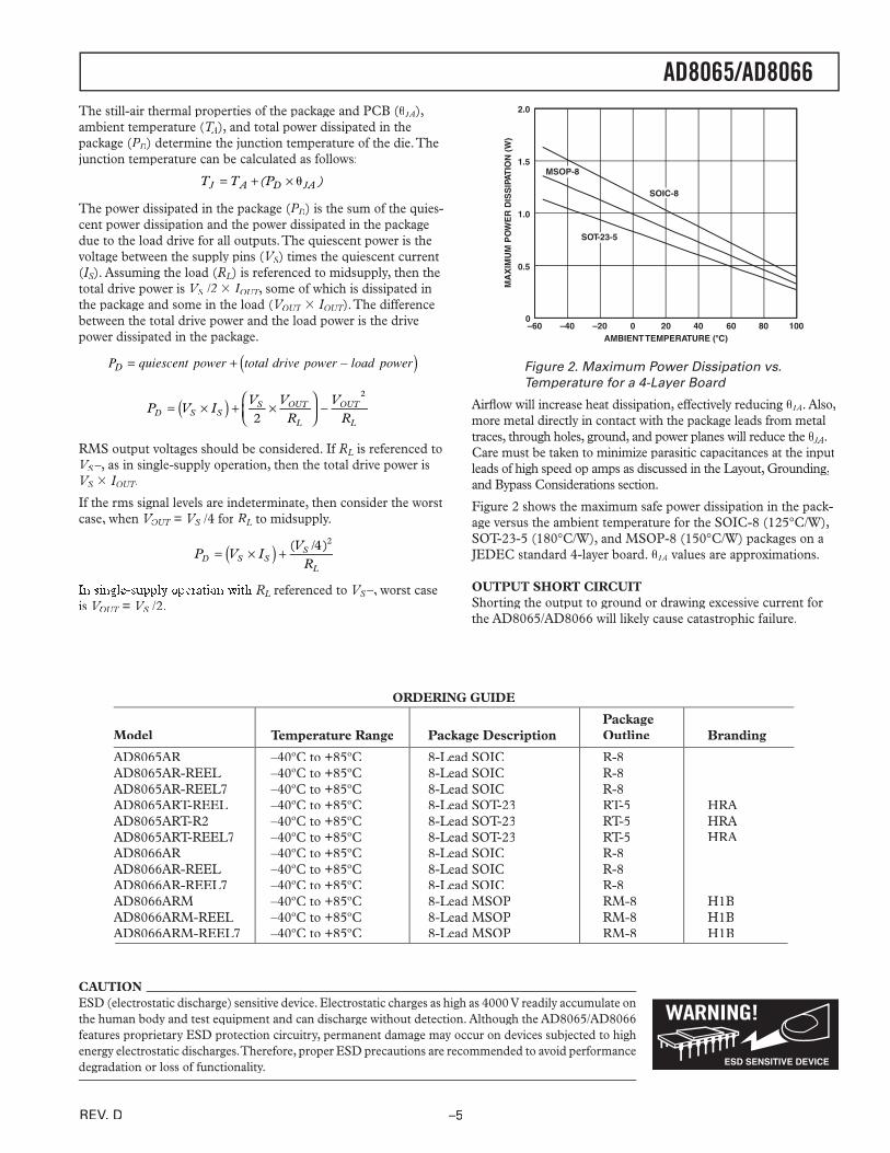
MAXIMUM POWER DISSIPATIONThe maximum safe power dissipation in the AD8065/AD8066 packages is limited by the associated rise in junction tempera-ture (TJture (TJture (T ) on the die. The plastic encapsulating the die will locally reach the junction temperature. At approximately 150°C, which is the glass transition temperature, the plastic will change its properties. Even temporarily exceeding this temperature limit may change the stresses that the package exerts on the die, permanently shifting the parametric performance of the AD8065/AD8066. Exceeding a junction temperature of 175°C for an extended period of time can result in changes in the sili-con devices, potentially causing failure.
(@ TA = 25C, VS = 5 V, RL = 1 k, unless otherwise noted.)
REV. D
AD8065/AD8066
–5–
CAUTIONESD (electrostatic discharge) sensitive device. Electrostatic charges as high as 4000 V readily ac cu mu late on the human body and test equipment and can discharge without detection. Although the AD8065/AD8066 features proprietary ESD pro tec tion circuitry, permanent damage may occur on devices subjected to high energy electrostatic discharges. Therefore, proper ESD pre cau tions are rec om mend ed to avoid per for mance deg ra da tion or loss of functionality.
The still-air thermal properties of the package and PCB (JAJAJ ), ambient temperature (TATAT ), and total power dissipated in the package (PDPDP ) determine the junction temperature of the die. The junction temperature can be calculated as follows:
T T (P )A D AJ J= + ×
The power dissipated in the package (PDPDP ) is the sum of the quies-cent power dissipation and the power dissipated in the package due to the load drive for all outputs. The quiescent power is the voltage between the supply pins (VSVSV ) times the quiescent current S) times the quiescent current S
(ISISI ). Assuming the load (S). Assuming the load (S RL) is referenced to midsupply, then the total drive power is VSVSV /2 S /2 S IOUT IOUT I , some of which is dissipated in OUT, some of which is dissipated in OUT
the package and some in the load (VOUTVOUTV IOUT IOUT I ). The difference OUT). The difference OUT
between the total drive power and the load power is the drive power dissipated in the package.
P quiescent power total drive power load powerD = + ( )–
P V IV V
RV
RD S SS OUT
L
OUT
L
= ×( ) + ×
−2
2
RMS output voltages should be considered. If RL is referenced to L is referenced to L
VSVSV –, as in single-supply operation, then the total drive power is S –, as in single-supply operation, then the total drive power is S
VSVSV IOUT IOUT I .
If the rms signal levels are indeterminate, then consider the worst case, when VOUTVOUTV = OUT = OUT VSVSV /4 for S /4 for S RL to midsupply.L to midsupply.L
P V IV
RD S SS
L
= ×( ) + ( / )4 2
In single-supply operation with RL referenced to L referenced to L VSVSV –, worst case S –, worst case S
is VOUTVOUTV = OUT = OUT VSVSV /2.S /2.S
AMBIENT TEMPERATURE (C)
2.0
1.5
0–60 100–40
MA
XIM
UM
PO
WE
R D
ISS
IPAT
ION
(W
)
–20 0 20 40 60 80
1.0
0.5
SOIC-8
SOT-23-5
MSOP-8
Figure 2. Maximum Power Dissipation vs. Temperature for a 4-Layer Board
Airfl ow will increase heat dissipation, effectively reducing JAJAJ . Also, more metal directly in contact with the package leads from metal traces, through holes, ground, and power planes will reduce the JAJAJ . Care must be taken to minimize parasitic capacitances at the input leads of high speed op amps as discussed in the Layout, Grounding, and Bypass Considerations section.
Figure 2 shows the maximum safe power dissipation in the pack-age versus the ambient temperature for the SOIC-8 (125°C/W), SOT-23-5 (180°C/W), and MSOP-8 (150°C/W) packages on a JEDEC standard 4-layer board. JAJAJ values are approximations.
OUTPUT SHORT CIRCUITShorting the output to ground or drawing excessive current for the AD8065/AD8066 will likely cause catastrophic failure.
ORDERING GUIDE
Package Model Temperature Range Package Description Outline Branding
AD8065AR –40ºC to +85ºC 8-Lead SOIC R-8AD8065AR-REEL AD8065AR-REEL AD8065AR-REEL –40ºC to +85ºC 8-Lead SOIC R-8AD8065AR-REEL7 –40ºC to +85ºC 8-Lead SOIC R-8AD8065ART-REEL –40ºC to +85ºC 8-Lead SOT-23 RT-5 HRAAD8065ART-R2 –40ºC to +85ºC 8-Lead SOT-23 RT-5 HRAAD8065ART-REEL7 –40ºC to +85ºC 8-Lead SOT-23 RT-5 HRAAD8066AR –40ºC to +85ºC 8-Lead SOIC R-8AD8066AR-REEL AD8066AR-REEL AD8066AR-REEL –40ºC to +85ºC 8-Lead SOIC R-8AD8066AR-REEL7 –40ºC to +85ºC 8-Lead SOIC R-8AD8066ARM –40ºC to +85ºC 8-Lead MSOP RM-8 H1BAD8066ARM-REEL –40ºC to +85ºC 8-Lead MSOP RM-8 H1BAD8066ARM-REEL7 –40ºC to +85ºC 8-Lead MSOP RM-8 H1B
REV. D

–6–
AD8065/AD8066–Typical Performance Characteristics(Default Conditions: 5 V, CL = 5 pF, RL = 1 k, VOUT = 2 V p-p, Temperature = 25C)
FREQUENCY (MHz)
24
0.1 1000
GA
IN (
dB
)
9
1 10 100
21
18
15
12
6
3
0
–3
–6
G = +10
G = +5
G = +2
G = +1
VO = 200mV p-p
TPC 1. Small Signal Frequency Response for Various Gains
FREQUENCY (MHz)
6
0.1 1000
GA
IN (
dB
)
0
1 10 100
4
2
–2
–4
–6
VS = 5V
G = +1
VO = 200mV p-p
VS = 5V
VS = 12V
TPC 2. Small Signal Frequency Response for Various Supplies (See Test Circuit 1)
FREQUENCY (MHz)
2
0.1 1000
GA
IN (
dB
)
–1
1 10 100
1
0
–2
–3
–4
G = +1
VS = 5V
VS = 12V
–5
VO = 2V p-p
TPC 3. Large Signal Frequency Response for Various Supplies (See Test Circuit 1)
FREQUENCY (MHz)
6.9
0.1
GA
IN (
dB
) 6.5
1 10 100
6.4
6.3
6.2
G = +2
VOUT = 0.2V p-p
6.0
RL = 150
VOUT = 0.7V p-p
VOUT = 1.4V p-p
6.8
6.7
6.6
6.1
5.9
TPC 4. 0.1 dB Flatness Frequency Response(See Test Circuit 2)
FREQUENCY (MHz)
9
0.1 1000
GA
IN (
dB
)
6
1 10 100
8
7
5
4
3
VS = 5V
G = +2
VO = 200mV p-p
VS = 5V
VS = 12V
TPC 5. Small Signal Frequency Response for Various Supplies (See Test Circuit 2)
FREQUENCY (MHz)
0.1 1000
GA
IN (
dB
)
6
1 10 100
8
7
5
4
3
VS = 5V
G = +2
VS = 5VVS = 12V
2
1
0
TPC 6. Large Signal Frequency Response for Various Supplies (See Test Circuit 2)
REV. D
AD8065/AD8066
–7–
FREQUENCY (MHz)
9
6
–90.1 10001 10 100
3
–6
–3
0
VO = 200mV p-p
G = +1
CL = 5pF
CL = 25pFRsnub = 20
CL = 25pF
CL = 20pF
GA
IN (
dB
)
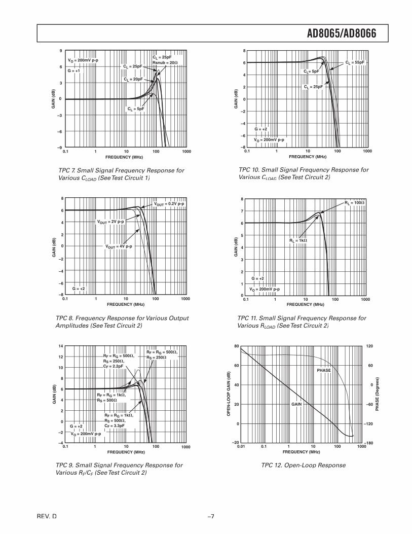
TPC 7. Small Signal Frequency Response for Various CLOADVarious CLOADVarious C (See Test Circuit 1)LOAD (See Test Circuit 1)LOAD
FREQUENCY (MHz)
8
6
–80.1 10001
GA
IN (
dB
)
10 100
4
2
–6
0
–2
–4
VOUT = 2V p-p
VOUT = 4V p-p
VOUT = 0.2V p-p
G = +2
TPC 8. Frequency Response for Various Output Amplitudes (See Test Circuit 2)
FREQUENCY (MHz)
14
12
–40.1 10001
GA
IN (
dB
)
10 100
10
8
–2
6
4
2
0
VO = 200mV p-p
G = +2
RF = RG = 500,RS = 250
RF = RG = 1k,RS = 500,CF = 3.3pF
RF = RG = 1k,RS = 500
RF = RG = 500,RS = 250,CF = 2.2pF
TPC 9. Small Signal Frequency Response forVarious RF/CF/CF F/CF/C (See Test Circuit 2) F (See Test Circuit 2) F
FREQUENCY (MHz)
8
6
–80.1 10001
GA
IN (
dB
)
10 100
4
2
–6
0
–2
–4G = +2
VO = 200mV p-p
CL = 25pF
CL = 55pF
CL= 5pF
TPC 10. Small Signal Frequency Response for Various CLOADVarious CLOADVarious C (See Test Circuit 2)LOAD (See Test Circuit 2)LOAD
FREQUENCY (MHz)
8
7
010001
GA
IN (
dB
)
10 100
6
5
1
4
3
2
0.1
G = +2
VO = 200mV p-p
RL = 100
RL = 1k
TPC 11. Small Signal Frequency Response for Various RLOAD (See Test Circuit 2)LOAD (See Test Circuit 2)LOAD
FREQUENCY (MHz)
80
60
–200.01 0.1
OP
EN
-LO
OP
GA
IN (
dB
)
1 10 100
40
20
0
120
60
–180
0
–60
–120
PH
AS
E (
Deg
rees
)
1000
GAIN
PHASE
TPC 12. Open-Loop Response
REV. D

AD8065/AD8066
–8–
FREQUENCY (MHz)0.1 1001 10
–30
–40
–120
DIS
TO
RT
ION
(d
Bc)
–50
–60
–100
–70
–80
–90
–110
G = +2
HD3 RL = 150
HD3 RL = 1k
HD2 RL = 150
HD2 RL = 1k
TPC 13. Harmonic Distortion vs. Frequency for Various Loads (See Test Circuit 2)
G = +2
HD3 RL = 150
HD2 RL = 150
HD2 RL = 300
VS = 12VF = 1MHz
HD3 RL = 300
OUTPUT AMPLITUDE (V p-p)0 131 2 3 4 5 6 7 8 9 10 11 12
–40
–50
DIS
TO
RT
ION
(d
Bc)
–90
–100
–110
–120
–70
–80
–60
14 15
–30
TPC 14. Harmonic Distortion vs. Amplitude forVarious Loads VSVarious Loads VSVarious Loads V = ±12 V (See Test Circuit 2)S = ±12 V (See Test Circuit 2)S
FREQUENCY (MHz)
INT
ER
CE
PT
PO
INT
(d
Bm
)
50
20
1 10
VS = 5V
VS = +5V
40
15
45
35
30
25
RL = 100VS = 12V
TPC 15. Third-Order Intercept vs. Frequencyand Supply Voltage
FREQUENCY (MHz)0.1 1001 10
–40
DIS
TO
RT
ION
(d
Bc)
–50
–60
–100
–70
–80
–90
–110
HD3 G = +2
HD3 G = +1
HD2 G = +2
HD2 G = +1
TPC 16. Harmonic Distortion vs. Frequency for Various Gains (See Test Circuits 1 and 2)
FREQUENCY (MHz)
–20
–30
–1200.1 101
DIS
TO
RT
ION
(d
Bc)
–40
–50
–60
–70
–80
–90
–100
–110
G = +2VS = 12V HD2 VO = 20V p-p
HD3 VO = 2V p-p
HD2 VO = 2V p-p
HD3 VO = 20V p-p
HD2 VO = 10V p-p
HD3 VO = 10V p-p
TPC 17. Harmonic Distortion vs. Frequency forVarious Amplitudes (See Test Circuit 2)
FREQUENCY (Hz)
100
110 10M
10
100 1k 10k 100k 1M 100M 1G
NO
ISE
(n
V/Hz)
TPC 18. Voltage Noise
REV. D

AD8065/AD8066
–9–
G = +1
50mV/DIV 20ns/DIV
TPC 19. Small Signal Transient Response 5 V Supply (See Test Circuit 11)
G = +1
2V/DIV 80ns/DIV
VS = 12V
VOUT = 2V p-p
VOUT = 4V p-p
VOUT = 10V p-p
TPC 20. Large Signal Transient Response(See Test Circuit 1)
G = 1
1.5V/DIV 100ns/DIV
IN OUT
TPC 21. Output Overdrive Recovery (See TestCircuit 3), VSCircuit 3), VSCircuit 3), V = ±5 VS = ±5 VS
G = +1
50mV/DIV 20ns/DIV
CL = 20pFCL = 5pF
TPC 22. Small Signal Transient Response ±5 V(See Test Circuit 1)
5µsG = +2
2V/DIV 80ns/DIV
VS = 12VVOUT = 10V p-p
VOUT = 2V p-p
TPC 23. Large Signal Transient Response(See Test Circuit 2)
G = +1
1.5V/DIV 100ns/DIV
IN
OUT
TPC 24. Input Overdrive Recovery (See Test Circuit 1), VS(See Test Circuit 1), VS(See Test Circuit 1), V = ±5 VS = ±5 VS
REV. D

AD8065/AD8066
–10–
t = 0
64s/DIV2mV/DIV
+0.1%
–0.1%
VIN = 140mV/DIV
VOUT – 2VIN
TPC 25. Long-Term Settling Time (See Test Circuit 8)
TEMPERATURE ( C)
0
–3025 8535
INP
UT
BIA
S C
UR
RE
NT
(p
A)
45 55 65 75
–5
–10
–15
–20
–25
–Ib
+Ib
TPC 26. Input Bias Current vs. Temperature
COMMON-MODE VOLTAGE (V)
0.3
0
–0.3–14 12–12
OF
FS
ET
VO
LT
AG
E (
mV
)
–10 –8 –6 –4 –2 0 2 4 6 8 10
0.2
0.1
–0.1
–0.2
14
VS = +5V
VS = 12V
VS = 5V
TPC 27. Input Offset Voltage vs. Common-Mode Voltage
0.1%
2mV/DIV 10ns/DIV
0.1%t = 0
VOUT – 2VIN
VIN = 500mV/DIV
TPC 28. 0.1% Short-Term Settling Time(See Test Circuit 8)
0I b
(
A)
3630241812
6
–5
–15
–25
–30
0
I b (
pA
)
–12 8–2–10 0–8 2–6 4–4 6COMMON-MODE VOLTAGE (V)
10 12
42
–Ib
+Ib
–Ib
+Ib
FET INPUT STAGE
BJT INPUT STAGE
–20
–10
5
TPC 29. Input Bias Current vs. Common-Mode Voltage Range*
INPUT OFFSET VOLTAGE (mV)
35
15
0–2.0 2.0–1.5 –1.0 –0.5 0 0.5 1.0 1.5
30
20
10
5
40
25
N = 299SD = 0.388MEAN = –0.069
TPC 30. Input Offset Voltage
*See Input and Output Overload Behavior Section
REV. D

AD8065/AD8066
–11–
FREQUENCY (MHz)0.1 1001 10
–30C
MR
R (
dB
)
–40
–50
–90
–60
–70
–80
–100
VS = 5V
VS = 12V
TPC 31. CMRR vs. Frequency (See Test Circuit 5)
I LOAD (mA)
0.30
0.25
00 4010
OU
TP
UT
SA
TU
RA
TIO
N V
OL
TA
GE
(V
)
20 30
0.20
0.15
0.10
0.05
VOL – VEE
VCC – VOH
TPC 32. Output Saturation Voltage vs. Output Load Current
FREQUENCY (MHz)
0
–10
–90
0.01 10000.1
PS
RR
(d
B)
1 10 100
–20
–30
–70
–40
–50
–60
–80
+ PSRR
– PSRR
–100
TPC 33. PSRR vs. Frequency (See Test Circuits 7 and 9)
FREQUENCY (Hz)1k 100M10k
OU
TP
UT
IMP
ED
AN
CE
(
)
100k 1M 10M
G = +1
G = +2
0.01
100
100
10
1
0
0.1
TPC 34. Output Impedance vs. Frequency (See Test Circuits 4 and 6)
TEMPERATURE ( C)
80
3025 8535
OU
TP
UT
SA
TU
RA
TIO
N V
OL
TA
GE
(m
V)
45 55 65 75
75
60
45
40
35
70
65
55
50
VOL – VEE
VCC – VOH
TPC 35. Output Saturation Voltage vs. Temperature
FREQUENCY (MHz)0.1 1
CR
OS
STA
LK
(d
B)
10 100–90
–80
–70
–60
–50
–40
–30
–20
–10
0
B TO A
A TO B
VIN = 2V p-pG = +1
TPC 36. Crosstalk vs. Frequency (See Test Circuit 10)
REV. D
AD8065/AD8066
–12–
TEMPERATURE ( C)
6.60
6.25–40 80–20
SU
PP
LY
CU
RR
EN
T (
mA
)
0 20 40 60
6.55
6.50
6.45
6.35
6.30
6.40
VS = +5V
VS = 12V
VS = 5V
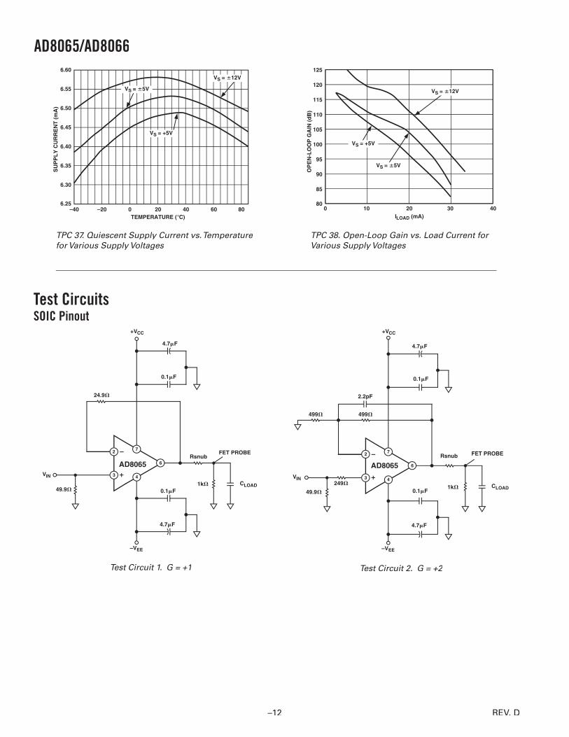
TPC 37. Quiescent Supply Current vs. Temperature for Various Supply Voltages
ILOAD (mA)
125
120
800 4010
OP
EN
-LO
OP
GA
IN (
dB
)
20 30
105
95
90
85
115
110
100
VS = 5V
VS = +5V
VS = 12V
TPC 38. Open-Loop Gain vs. Load Current forVarious Supply Voltages
AD8065
+VCC
VIN
–VEE
4.7F
0.1F
2.2pF
Rsnub
0.1F
4.7F
49.9
499 499
249 CLOAD
FET PROBE
1k
Test Circuit 2. G = +2
AD8065
+VCC
VIN
–VEE
4.7F
0.1F
24.9
Rsnub
0.1F
4.7F
CLOAD
FET PROBE
49.91k
Test Circuit 1. G = +1
Test CircuitsSOIC Pinout
REV. D
AD8065/AD8066
–13–
VIN
49.9
AD8065
+VCC
–VEE
4.7F
0.1F
2.2pF
0.1F
4.7F
499 499
249
FET PROBE
1k
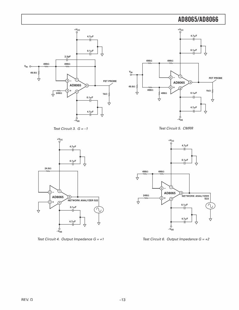
Test Circuit 3. G = –1
AD8065
+VCC
–VEE
4.7F
0.1F
24.9
0.1F
4.7F
NETWORK ANALYZER S22
Test Circuit 4. Output Impedance G = +1
VIN
49.9
AD8065
+VCC
–VEE
4.7F
0.1F
0.1F
4.7F
499 499
FET PROBE
1k499
499
Test Circuit 5. CMRR
AD8065
+VCC
–VEE
0.1F
4.7F
499 499
249 NETWORK ANALYZERS22
4.7F
0.1F
Test Circuit 6. Output Impedance G = +2
REV. D
AD8065/AD8066
–14–
AD8065
–VEE
24.9
0.1F
4.7F
+VCC
FET PROBE
1k
VIN1V p-p
49.9
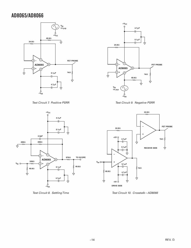
Test Circuit 7. Positive PSRR
AD8065
+VCC
VIN
–VEE
4.7F
0.1F
2.2pF
976
0.1F
4.7F
499 499
249
TO SCOPE
49.949.9
Test Circuit 8. Settling Time
AD8065
+VCC
–VEE
4.7F
0.1F
FET PROBE
49.9
24.9
VIN1V p-p
1k
Test Circuit 9. Negative PSRR
24.9
49.9
24.9
1k
0.1F
4.7F
VIN
+5V
–5V
1k
DRIVE SIDE
RECEIVE SIDE0.1F
4.7F
FET PROBE
Test Circuit 10. Crosstalk—AD8066
REV. D
AD8065/AD8066
–15–
249
0.1F
VIN
1.5V
1.5V
1.5V
4.7F
499499
5V
49.9
2.2pF
1k
FET PROBE
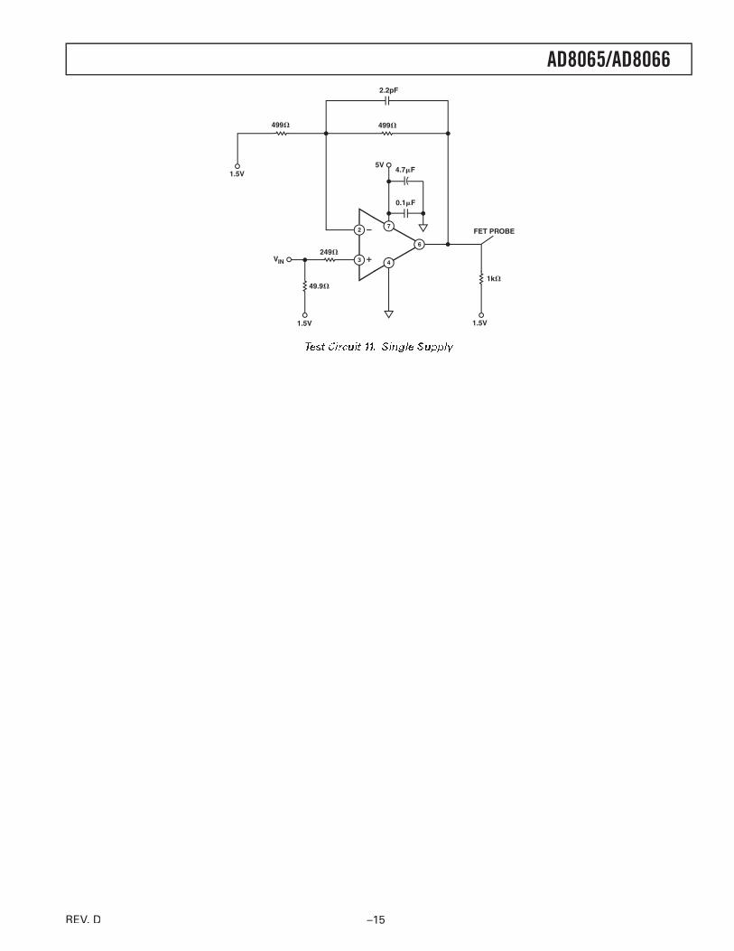
Test Circuit 11. Single Supply
REV. D

AD8065/AD8066
–16–
THEORY OF OPERATIONThe AD8065/AD8066 are voltage feedback operational ampli-fi ers that combine a laser-trimmed JFET input stage with Analog Devices’ eXtra Fast Complementary Bipolar process, resulting in an outstanding combination of precision and speed. Supply voltage range is from 5 V to 24 V. The amplifi ers feature a patented rail-to-rail output stage capable of driving within 0.5 V of either power supply while sourcing or sinking up to 30 mA. Also featured is a single-supply input stage that handles common-mode signals from below the negative supply to within 3 V of the positive rail. Operation beyond the JFET input range is possible because of an auxiliary bipolar input stage that functions with input voltages up to the positive supply. The amplifi ers operate as if they have a rail-to-rail input and exhibit no phase reversal behavior for common-mode voltages within the power supply.
With voltage noise of 7 nV/HzHzHzHz and –88 dBc distortion for 1 MHz Hz and –88 dBc distortion for 1 MHz Hz2 V p-p signals, the AD8065/AD8066 are a great choice for high resolution data acquisition systems. Their low noise, sub-pA input current, precision offset, and high speed make them superb pre-amps for fast photodiode applications. The speed and output drive capability of the AD8065/AD8066 also make them useful in video applications.
Closed-Loop Frequency ResponseThe AD8065/AD8066 are classic voltage feedback amplifi ers with an open-loop frequency response that can be approximated as the integrator response shown in Figure 3. Basic closed-loop frequency response for inverting and noninverting confi gurations can be derived from the schematics shown.
Noninverting Closed-Loop Frequency ResponseSolving for the transfer function
VV
f R RR R s f R
O
I
crossover G F
F G crossover G
= × ++ + × ×2
2π
π( )
( )
where fcrossoverfcrossoverf is the frequency where the amplifi er’s open-loop crossover is the frequency where the amplifi er’s open-loop crossover
gain equals 0 db.
At dcVV
R RR
O
I
F G
G
= +
Closed-loop –3 dB frequency
f fR
R RdB crossoverG
F G− = ×
+3
Inverting Closed-Loop Frequency Response
VV
f Rs R R f R
O
I
crossover F
F G crossover G
= − × ×+ + × ×
22
ππ( )
At dcVV
RR
O
I
F
G
= −
Closed-loop –3 dB frequency
f fR
R RdB crossoverG
F G− = ×
+3
RF
AVO
RG
VIVE
FREQUENCY (MHz)
80
60
0.01 100
OP
EN
-LO
OP
GA
IN (
A)
(dB
)
0.1 1 10
40
20
0
fcrossover = 65MHz
A = (2fcrossover)/s
RF
VE AVO
RG VI
Figure 3. Open-Loop Gain vs. Frequency and Basic Connections
REV. D

AD8065/AD8066
–17–
The closed-loop bandwidth is inversely proportional to the noise gain of the op amp circuit, (RF + RF + RF G )/RG )/RG G. This simple model is accurate for noise gains above 2. The actual bandwidth of circuits with noise gains at or below 2 will be higher than those predicted with this model due to the infl uence of other poles in the frequency response of the real op amp.
VO
RF
A
RG
VI
Ib– RS
Ib+
+VOS –
Figure 4. Voltage Feedback Amplifi er DC Errors
Figure 4 shows a voltage feedback amplifi er’s dc errors. For both inverting and noninverting confi gurations
V (error) I RR R
RI R V
R RRO b+ S
G F
Gb - F OS
G F
G= × +
− × + +
The voltage error due to Ib+Ib+I and Ib–Ib–I is minimized if b– is minimized if b– RS = S = S RF RG
(though with the AD8065 input currents at less than 20 pA over temp erature, this is likely not a concern). To include common- mode and power supply rejection effects, total VOSVOSV can be OS can be OS
modeled as
V VV
PSRV
CMROS OSnomS CM= + +∆ ∆
VOSVOSV nomOSnomOS is the offset voltage specifi ed at nominal conditions. VSVSV is S is S
the change in power supply from nominal conditions. PSR is the PSR is the PSRpower supply rejection. VCMVCMV is the change in common-mode vol-CM is the change in common-mode vol-CM
tage from nominal conditions. CMR is the common-mode rejection.CMR is the common-mode rejection.CMR
Wideband OperationTest circuits 1, 2, and 3 show the circuits used for wideband characterization for gains of +1, +2, and –1. Source impedance at the summing junction (RF RG) will form a pole in the amplifi er’s loop response with the amplifi er’s input capacitance of 6.6 pF. This can cause peaking and ringing if the time constant formed is too low. Feedback resistances of 300 to 1 k are recommended, since they will not unduly load down the amplifi er and the time constant formed will not be too low. Peaking in the frequency response can be compensated with a small capacitor (CFCFC ) in parallel F) in parallel F
with the feedback resistor, as illustrated in TPC 9. This shows the effect of different feedback capacitances on the peaking and bandwidth for a noninverting G = +2 amplifi er.
For the best settling times and the best distortion, the impedances at the AD8065/AD8066 input terminals should be matched. This minimizes nonlinear common-mode capacitive effects that can degrade ac performance.
Actual distortion performance depends on a number of variables:
• The closed-loop gain of the application
• Whether it is inverting or noninverting
• Amplifi er loading
• Signal frequency and amplitude
• Board layout
Also see TPCs 13 to 17. The lowest distortion will be obtained with the AD8065 used in low gain inverting applications, since this eliminates common-mode effects. Higher closed-loop gains result in worse distortion performance.
Input ProtectionThe inputs of the AD8065/AD8066 are protected with back-to-back diodes between the input terminals as well as ESD diodes to either power supply. This results in an input stage with picoamps of input current that can withstand up to 1500 V ESD events (human body model) with no degradation.
Excessive power dissipation through the protection devices will destroy or degrade the performance of the amplifi er. Differential voltages greater than 0.7 V will result in an input current of approxi-mately (|V+V+V – V– – V– – V |– 0.7 V)/V)/V RIRIR , where I, where I RIRIR is the resistance in series I is the resistance in series I
with the inputs. For input voltages beyond the positive supply, the input current will be approximately (VIinput current will be approximately (VIinput current will be approximately (V – VCC – 0.7)/R – 0.7)/R – 0.7)/ IRIR . Beyond the negative supply, the input current will be about (VI – VEE + 0.7)/RIRIR . If the inputs of the amplifi er are to be subjected to sustained dif-ferential voltages greater than 0.7 V or to input voltages beyond the amplifi er power supply, input current should be limited to 30 mA by an appropriately sized input resistor (RIRIR ) as shown in Figure 5.I) as shown in Figure 5.I
RI VI VO
AD8065
RI >(| V+– V– | – 0.7V)
30mA
FOR LARGE | V+ – V– |
RI >(VI – VEE – 0.7V)
30mA
RI > (VI – VEE + 0.7V)
30mAFOR VI BEYONDSUPPLY VOLTAGES
Figure 5. Current Limiting Resistor
Thermal ConsiderationsWith 24 V power supplies and 6.5 mA quiescent current, the AD8065 dissipates 156 mW with no load. The AD8065/AD8066 dissipate 312 mW. This can lead to noticeable thermal effects, especially in the small SOT-23-5 (thermal resistance of 160ºC/W). VOSVOSV temperature drift is trimmed to guarantee a max drift of OS temperature drift is trimmed to guarantee a max drift of OS
17 µV/°C, so it can change up to 0.425 mV due to warm-up effects for an AD8065/AD8066 in a SOT-23-5 package on 24 V.
IbIbI increases by a factor of 1.7 for every 10ºC rise in temperature. IbIbI will be close to 5 times higher at 24 V supplies as opposed to a single 5 V supply.
Heavy loads will increase power dissipation and raise the chip junction temperature as described in the Maximum Power Dissipa-tion section. Care should be taken to not exceed the rated power dissipation of the package.
REV. D

AD8065/AD8066
–18–
Input and Output Overload BehaviorThe AD8065/AD8066 have internal circuitry to guard against phase reversal due to overdriving the input stage. A simplifi ed schematic of the input stage, including the input-protection diodes and antiphase reversal circuitry, is shown in Figure 6.
The circuit is arranged such that when the input common-mode voltage exceeds a certain threshold, the input JFET pair’s bias current will turn OFF, and the bias current of an auxiliary NPN pair will turn ON, taking over control of the amplifi er. When the input common-mode voltage returns to a viable operating value, the FET stage turns back ON, the NPN stage turns OFF, and normal operation resumes.
The NPN pair can sustain operation with the input voltage up to the positive supply, so this is a pseudo rail-to-rail input stage. For operation beyond the FET stage’s common-mode limit, the amplifi er’s VOSVOSV will change to the NPN pair’s offset (mean of OS will change to the NPN pair’s offset (mean of OS
160 µV, standard deviation of 820 µV), and IbIbI will increase to the NPN pair’s base current up to 45 µA (see TPC 29).
Switchback, or recovery time, is about 100 ns, as shown in TPC 24.
The output transistors of the rail-to-rail output stage have circuitry to limit the extent of their saturation when the output is overdriven. This helps output recovery time. Output recovery from a 0.5 V output overdrive on a ±5 V supply is shown in TPC 21.
LAYOUT, GROUNDING, AND BYPASSING CONSIDERATIONSPower Supply BypassingPower supply pins are actually inputs and care must be taken so that a noise-free stable dc voltage is applied. The purpose of bypass capacitors is to create low impedances from the supply to ground at all frequencies, thereby shunting or fi ltering most of the noise.
Decoupling schemes are designed to minimize the bypassing imped-ance at all frequencies with a parallel combination of capacitors. 0.1 µF (X7R or NPO) chip capacitors are critical and should be as close as possible to the amplifi er package. The 4.7 µF tantalum capacitor is less critical for high frequency bypassing, and in most cases, only one is needed per board, at the supply inputs.
GroundingA ground plane layer is important in densely packed PC boards to spread the current minimizing parasitic inductances. However, an understanding of where the current fl ows in a circuit is critical to implementing effective high speed circuit design. The length of the current path is directly proportional to the magnitude of parasitic inductances and therefore the high frequency impedance of the path. High speed currents in an inductive ground return will create an unwanted voltage noise.
VTHRESHOLD
VBIAS
S
VP
TO REST OF AMP
VEE
VCC
S
VN
Figure 6. Simplifi ed Input Stage
REV. D

AD8065/AD8066
–19–
The length of the high frequency bypass capacitor leads is most critical. A parasitic inductance in the bypass grounding will work against the low impedance created by the bypass capacitor. Place the ground leads of the bypass capacitors at the same physical location. Because load currents fl ow from the supplies as well, the ground for the load impedance should be at the same physical location as the bypass capacitor grounds. For the larger value capacitors, which are intended to be effective at lower frequencies, the current return path distance is less critical.
Leakage CurrentsPoor PC board layout, contaminants, and the board insulator material can create leakage currents that are much larger than the input bias current of the AD8065/AD8066. Any voltage differential between the inputs and nearby runs will set up leakage currents through the PC board insulator, for example, 1 V/100 G = 10 pA. Similarly, any contaminants on the board can create signifi cant leakage (skin oils are a common problem). To signifi cantly reduce leakages, put a guard ring (shield) around the inputs and input leads that are driven to the same voltage potential as the inputs. This way there is no voltage potential between the inputs and surrounding area to set up any leakage currents. For the guard ring to be com-pletely effective, it must be driven by a relatively low impedance source and should completely surround the input leads on all sides, above and below, using a multilayer board.
Another effect that can cause leakage currents is the charge absorp-tion of the insulator material itself. Minimizing the amount of material between the input leads and the guard ring will help to reduce the absorption. Also, low absorption materials, such as Tefl on® or ceramic, may be necessary in some instances.
Input CapacitanceAlong with bypassing and ground, high speed amplifi ers can be sensitive to parasitic capacitance between the inputs and ground. A few pF of capacitance will reduce the input impedance at high fre-quencies, in turn increasing the amplifi er’s gain, causing peaking of the frequency response or even oscillations, if severe enough. It is recommended that the external passive components connected to the input pins be placed as close as possible to the inputs to avoid parasitic capacitance. The ground and power planes must be kept at a small distance from the input pins on all layers of the board.
Output CapacitanceTo a lesser extent, parasitic capacitances on the output can cause peaking and ringing of the frequency response. There are two methods to effectively minimize their effect.
1) As shown in Figure 7, put a small value resistor (RS) in series S) in series S
with the output to isolate the load capacitor from the amp’s output stage. A good value to choose is 20 (see TPC 7).
RS = 20
VI
AD8065CL
VO
Figure 7. Output Isolation Resistor
2) Increase the phase margin with higher noise gains or add a pole with a parallel resistor and capacitor from –IN to the output.
RSH = 1011
VO
RF
CF
CM
RF
CM
CD
CF + CS
CS
VB
IPHOTO
Figure 8. Wideband Photodiode Preamp
REV. D
AD8065/AD8066
–20–
Input-to-Output CouplingIn order to minimize capacitive coupling between the inputs and output, the output signal traces should not be parallel with inputs.
Wideband Photodiode PreampFigure 8 shows an I/V converter with an electrical model of a photodiode. The basic transfer function is where
VI R
sC ROUTPHOTO F
F F
= ×+1
IPHOTOIPHOTOI is the output current of the photodiode, and the parallel combination of RF and F and F CFCFC set the signal bandwidth.F set the signal bandwidth.F
The stable bandwidth attainable with this preamp is a function of RF, the gain bandwidth product of the amplifi er, and the total F, the gain bandwidth product of the amplifi er, and the total F
capacitance at the amplifi er’s summing junction, including CSCSCand the amplifi er input capacitance. RF and the total capacitance F and the total capacitance F
produce a pole in the amplifi er’s loop transmission that can result in peaking and instability. Adding CFCFC creates a zero in the loop F creates a zero in the loop F
transmission that compensates for the pole’s effect and reduces the signal bandwidth. It can be shown that the signal bandwidth resulting in a 45° phase margin (fresulting in a 45° phase margin (fresulting in a 45° phase margin ( (45)f(45)f ) is defi ned by the expression
ffR C
CR
F S( )45 2
=× ×π
where:
fCRfCRf is the amplifi er crossover frequency.
RF is the feedback resistor.F is the feedback resistor.F
CSCSC is the total capacitance at the amplifi er summing junction S is the total capacitance at the amplifi er summing junction S
(amplifi er + photodiode + board parasitics).
The value of CFCFC that produces F that produces F f(45)f(45)f can be shown to be
CCR fF
S
F CR
=× ×2π
The frequency response in this case will show about 2 dB of peaking and 15% overshoot. Doubling CFCFC and cutting the band-F and cutting the band-F
width in half will result in a fl at frequency response, with about 5% transient overshoot.
The preamp’s output noise over frequency is shown in Figure 9.
FREQUENCY (Hz)
VO
LT
AG
E N
OIS
E (
nV
/Hz)
2RFCF
2RF (CF + CS + CM + 2CD)
(CS + CM + 2CD + CF) /CF
RF NOISE
VEN (CF + CS + CM + 2CD)/CFf3f2
f3 =
VEN
f1
f2 =
f1 =1
1
fCR
NOISE DUE TO AMPLIFIER
Figure 9. Photodiode Voltage Noise Contributions
The pole in the loop transmission translates to a zero in the ampli-fi er’s noise gain, leading to an amplifi cation of the input voltage noise over frequency. The loop transmission zero introduced by CFCFClimits the amplifi cation. The noise gain’s bandwidth extends past the preamp signal bandwidth and is eventually rolled off by the decreasing loop gain of the amplifi er. Keeping the input terminal impedances matched is recommended to eliminate common-mode noise peaking effects, which will add to the output noise.
Integrating the square of the output voltage noise spectral density over frequency and then taking the square root allows users to obtain the total rms output noise of the preamp. Table I summa-rizes approximations for the amplifi er and feedback and source resistances. Noise components for an example preamp with RF = 50 kF = 50 kF , CSCSC = 15 pF, and S = 15 pF, and S CFCFC = 2 pF (bandwidth of about F = 2 pF (bandwidth of about F
1.6 MHz) are also listed.
Table 1. RMS Noise Contributions of Photodiode Preamp
RMS Noise with RF =50 kContributor Expression CS = 15 pF, CS = 15 pF
RF RF R (2) 2 4 1 572× ×2 4× ×2 4 × ×2× ×2kT× ×kT× × R f2R f2× ×R f× ×2× ×2R f2× ×2FR fFR f 1 5.1 5 64.5 µV
Amp to f1Amp to f1Amp to f ven f× 1f1f 2.4 µV
Amp (f1–Amp (f1–Amp (f f1f1f ) ven
Cf fS M F D
F× ×
( )C C( )C C C C( )C CS M F( )S M FC CS M FC C( )C CS M FC C C CS M FC C( )C CS M FC CD( )D+ +( )+ +C C+ +C C( )C C+ +C CS M F+ +S M F( )S M F+ +S M FC CS M FC C+ +C CS M FC C( )C CS M FC C+ +C CS M FC C C C+C C( )C C+C Cf f–f f
C C( )C C2C C( )C C2 1f f2 1f f
31 µV
Amp to (past f2Amp to (past f2Amp to (past f ) ven
CfS M D F
F× × ×× ×f× ×f
( )C C( )C C C C( )C CS M D( )S M DC CS M DC C( )C CS M DC C C CS M DC C( )C CS M DC CF( )F+ +( )+ +C C+ +C C( )C C+ +C CS M D+ +S M D( )S M D+ +S M DC CS M DC C+ +C CS M DC C( )C CS M DC C+ +C CS M DC C C C+C C( )C C+C CC C( )C C2C C( )C C1 5.1 5. 73f3f× ×3× ×f× ×f3f× ×f
260 µV
270 µV (Total)
REV. D

AD8065/AD8066
–21–
High Speed JFET Input Instrumentation Amplifi erFigure 10 shows an example of a high speed instrumentation amplifi er with high input impedance using the AD8065/AD8066. The dc transfer function is
V V VROUT N P
G
= − +
( )1 1000
For G = +1, it is recommended that the feedback resistors for the two preamps be set to a low value (for instance 50 for 50 source impedance). The bandwidth for G = +1 will be 50 MHz. For higher gains, the bandwidth will be set by the preamp, equaling
Inamp-3dB = × ×( ) / ( )f R RCR G F2
Common-mode rejection of the inamp will be primarily deter-mined by the match of the resistor ratios R1:R2 to R3:R4. It can be estimated
VV
O
CM
= −+( )
( )δ δδ δ
1 2
1 1 2
The summing junction impedance for the preamps is equal to RF RF R 0.5(RG). This is the value to be used for matching purposes.
Video BufferThe output current capability and speed of the AD8065 make it useful as a video buffer, shown in Figure 11.
The G = +2 confi guration compensates for the voltage division of the signal due to the signal termination. This buffer maintains 0.1 dB fl atness for signals up to 7 MHz, from low amplitudes up to 2 V p-p (TPC 4). Differential gain and phase have been measured to be 0.02% and 0.028° at ±5 V supplies.
VS
4.7F0.1F
2.2pF
499
249
75
499
VI
AD8065
VS
4.7F0.1F75 VO
Figure 11. Video Buffer
VCC
VEE
1/2AD8066
4.7F0.1F
RS1
4.7F0.1F
VN 2.2pF
500
R2
VP
1/2AD8066
4.7F0.1F
4.7F0.1F
AD8065
4.7F0.1F
4.7F0.1F
VO
RG
VCC
VEE
VCC
VEE
500
R4
RS2
500
R1
500
R3 RF = 500
2.2pF
RF = 500
Figure 10. High Speed Instrumentation Amplifi er
REV. D
AD8065/AD8066
–22–
OUTLINE DIMENSIONS
8-Lead Standard Small Outline Package [SOIC]Narrow Body
(R-8)Dimensions shown in millimeters and (inches)
0.25 (0.0098)0.17 (0.0067)
1.27 (0.0500)0.40 (0.0157)
0.50 (0.0196)0.25 (0.0099)
45
80
1.75 (0.0688)1.35 (0.0532)
SEATINGPLANE
0.25 (0.0098)0.10 (0.0040)
8 5
41
5.00 (0.1968)4.80 (0.1890)
4.00 (0.1574)3.80 (0.1497)
1.27 (0.0500)BSC
6.20 (0.2440)5.80 (0.2284)
0.51 (0.0201)0.31 (0.0122)COPLANARITY
0.10
CONTROLLING DIMENSIONS ARE IN MILLIMETERS; INCH DIMENSIONS(IN PARENTHESES) ARE ROUNDED-OFF MILLIMETER EQUIVALENTS FORREFERENCE ONLY AND ARE NOT APPROPRIATE FOR USE IN DESIGN
COMPLIANT TO JEDEC STANDARDS MS-012AA
5-Lead Small Outline Transistor Package [SOT-23](RT-5)
Dimensions shown in millimeters
PIN 1
1.60 BSC 2.80 BSC
1.90BSC
0.95 BSC
1 3
4 5
2
0.220.08
1050
0.500.30
0.15 MAX SEATINGPLANE
1.45 MAX
1.301.150.90
2.90 BSC
0.600.450.30
COMPLIANT TO JEDEC STANDARDS MO-178AA
8-Lead Mini Small Outline Package [MSOP](RM-8)
Dimensions shown in millimeters
0.800.600.40
80
8 5
41
4.90BSC
PIN 10.65 BSC
3.00BSC
SEATINGPLANE
0.150.00
0.380.22
1.10 MAX
3.00BSC
COPLANARITY0.10
0.230.08
COMPLIANT TO JEDEC STANDARDS MO-187AA
REV. D
AD8065/AD8066
–23–
Revision HistoryLocation Page
11/03-Data Sheet changed from REV. C to REV. D.
Changes to FEATURES . . . . . . . . . . . . . . . . . . . . . . . . . . . . . . . . . . . . . . . . . . . . . . . . . . . . . . . . . . . . . . . . . . . . . . . . . . . . . . . . . . . 1
Changes to CONNECTION DIAGRAMS . . . . . . . . . . . . . . . . . . . . . . . . . . . . . . . . . . . . . . . . . . . . . . . . . . . . . . . . . . . . . . . . . . . . . 1
Updated ORDERING GUIDE . . . . . . . . . . . . . . . . . . . . . . . . . . . . . . . . . . . . . . . . . . . . . . . . . . . . . . . . . . . . . . . . . . . . . . . . . . . . . 5
Updated OUTLINE DIMENSIONS . . . . . . . . . . . . . . . . . . . . . . . . . . . . . . . . . . . . . . . . . . . . . . . . . . . . . . . . . . . . . . . . . . . . . . . . 22
4/03-Data Sheet changed from REV. B to REV. C.
Added SOIC-8 (R) for the AD8065 . . . . . . . . . . . . . . . . . . . . . . . . . . . . . . . . . . . . . . . . . . . . . . . . . . . . . . . . . . . . . . . . . . . . . . . . . . 4
2/03-Data Sheet changed from REV. A to REV. B.
Changes to ABSOLUTE MAXIMUM RATINGS . . . . . . . . . . . . . . . . . . . . . . . . . . . . . . . . . . . . . . . . . . . . . . . . . . . . . . . . . . . . . . . 4
Changes to Test Circuit 10 . . . . . . . . . . . . . . . . . . . . . . . . . . . . . . . . . . . . . . . . . . . . . . . . . . . . . . . . . . . . . . . . . . . . . . . . . . . . . . . . 14
Changes to Test Circuit 11 . . . . . . . . . . . . . . . . . . . . . . . . . . . . . . . . . . . . . . . . . . . . . . . . . . . . . . . . . . . . . . . . . . . . . . . . . . . . . . . . 15
Changes to Noninverting Closed-Loop Frequency Response . . . . . . . . . . . . . . . . . . . . . . . . . . . . . . . . . . . . . . . . . . . . . . . . . . . . . . 16
Changes to Inverting Closed-Loop Frequency Response . . . . . . . . . . . . . . . . . . . . . . . . . . . . . . . . . . . . . . . . . . . . . . . . . . . . . . . . . . 16
Updated Figure 6 . . . . . . . . . . . . . . . . . . . . . . . . . . . . . . . . . . . . . . . . . . . . . . . . . . . . . . . . . . . . . . . . . . . . . . . . . . . . . . . . . . . . . . . 18
Changes to Figure 7 . . . . . . . . . . . . . . . . . . . . . . . . . . . . . . . . . . . . . . . . . . . . . . . . . . . . . . . . . . . . . . . . . . . . . . . . . . . . . . . . . . . . . 19
Changes to Figures 10 . . . . . . . . . . . . . . . . . . . . . . . . . . . . . . . . . . . . . . . . . . . . . . . . . . . . . . . . . . . . . . . . . . . . . . . . . . . . . . . . . . . 21
Changes to Figure 11 . . . . . . . . . . . . . . . . . . . . . . . . . . . . . . . . . . . . . . . . . . . . . . . . . . . . . . . . . . . . . . . . . . . . . . . . . . . . . . . . . . . . 22
Changes to High Speed JFET Instrumentation Amplifi er . . . . . . . . . . . . . . . . . . . . . . . . . . . . . . . . . . . . . . . . . . . . . . . . . . . . . . . . . 22
Changes to Video Buffer . . . . . . . . . . . . . . . . . . . . . . . . . . . . . . . . . . . . . . . . . . . . . . . . . . . . . . . . . . . . . . . . . . . . . . . . . . . . . . . . . . 22
8/02-Data Sheet changed from REV. 0 to REV. A.
Added AD8066 . . . . . . . . . . . . . . . . . . . . . . . . . . . . . . . . . . . . . . . . . . . . . . . . . . . . . . . . . . . . . . . . . . . . . . . . . . . . . . . . . . . Universal
Added SOIC-8 (R) and MSOP-8 (RM) . . . . . . . . . . . . . . . . . . . . . . . . . . . . . . . . . . . . . . . . . . . . . . . . . . . . . . . . . . . . . . . . . . . . . . . 1
Edits to GENERAL DESCRIPTION . . . . . . . . . . . . . . . . . . . . . . . . . . . . . . . . . . . . . . . . . . . . . . . . . . . . . . . . . . . . . . . . . . . . . . . . 1
Edits to SPECIFICATIONS . . . . . . . . . . . . . . . . . . . . . . . . . . . . . . . . . . . . . . . . . . . . . . . . . . . . . . . . . . . . . . . . . . . . . . . . . . . . . . . 2
New Figure 2 . . . . . . . . . . . . . . . . . . . . . . . . . . . . . . . . . . . . . . . . . . . . . . . . . . . . . . . . . . . . . . . . . . . . . . . . . . . . . . . . . . . . . . . . . . . 5
Changes to ORDERING GUIDE . . . . . . . . . . . . . . . . . . . . . . . . . . . . . . . . . . . . . . . . . . . . . . . . . . . . . . . . . . . . . . . . . . . . . . . . . . . 5
Edits to TPCs 18, 25, and 28 . . . . . . . . . . . . . . . . . . . . . . . . . . . . . . . . . . . . . . . . . . . . . . . . . . . . . . . . . . . . . . . . . . . . . . . . . . . . . . . 8
New TPC 36 . . . . . . . . . . . . . . . . . . . . . . . . . . . . . . . . . . . . . . . . . . . . . . . . . . . . . . . . . . . . . . . . . . . . . . . . . . . . . . . . . . . . . . . . . . 11
Added Test Circuits 10 and 11 . . . . . . . . . . . . . . . . . . . . . . . . . . . . . . . . . . . . . . . . . . . . . . . . . . . . . . . . . . . . . . . . . . . . . . . . . . . . . 14
MSOP (RM-8) added . . . . . . . . . . . . . . . . . . . . . . . . . . . . . . . . . . . . . . . . . . . . . . . . . . . . . . . . . . . . . . . . . . . . . . . . . . . . . . . . . . . 23
REV. D

C02
916–
0–11
/03(
D)
–24–


![Untitled Document [instrumentation.obs.carnegiescience.edu]instrumentation.obs.carnegiescience.edu/ccd/parts/AM29F040B.pdf · A0–A18 = Address Inputs DQ0–DQ7 = Data Input/Output](https://img.pdfslide.us/doc/110x75/5f55abc6e8d2ef0791257dfb/untitled-document-a0aa18-address-inputs-dq0adq7-data-inputoutput-ce.jpg)