Embed Size (px)
Citation preview
This content has been downloaded from IOPscience. Please scroll down to see the full text.
Download details:
IP Address: 134.129.115.40
This content was downloaded on 03/07/2014 at 06:29
Please note that terms and conditions apply.
A voltage uniformity study in large-area reactors for RF plasma deposition
View the table of contents for this issue, or go to the journal homepage for more
1997 Plasma Sources Sci. Technol. 6 170
(http://iopscience.iop.org/0963-0252/6/2/010)
Home Search Collections Journals About Contact us My IOPscience

Plasma Sources Sci. Technol. 6 (1997) 170–178. Printed in the UK PII: S0963-0252(97)81417-X
A voltage uniformity study inlarge-area reactors for RF plasmadeposition
L Sansonnens †‖, A Pletzer †‡, D Magni †, A A Howling †,Ch Hollenstein † and J P M Schmitt §
† Centre de Recherches en Physique des Plasmas, Ecole Polytechnique Federalede Lausanne, PPH—Ecublens, CH-1015 Lausanne, Switzerland‡ Association Euratom–Confederation Suisse, Switzerland§ Balzers Process Systems, 5 Rue Leon Blum, F-91120 Palaiseau, France
Received 23 September 1996, in final form 13 January 1997
Abstract. Non-uniform voltage distribution across the electrode area results ininhomogeneous thin-film RF plasma deposition in large-area reactors. In this work,a two-dimensional analytic model for the calculation of the voltage distributionacross the electrode area is presented. The results of this model are in goodagreement with measurements performed without plasma at 13.56 MHz and70 MHz in a large-area reactor. The principal voltage inhomogeneities are causedby logarithmic singularities in the vicinity of RF connections and not by standingwaves. These singularities are only described by a two-dimensional model andcannot be intuitively predicted by analogy to a one-dimensional case. Plasma lightemission measurements and thickness homogeneity studies of a-Si:H depositedfilms show that the plasma reproduces these voltage inhomogeneities.Improvement of the voltage uniformity is investigated by changing the number andposition of the RF connections.
1. Introduction
Plasma enhanced chemical vapour deposition (PECVD)of thin films such as amorphous silicon or silicon oxidehas widespread applications, especially in the field ofphotovoltaic solar cells and thin-film transistors for flatscreen production. Industrial applications require highdeposition rates over large areas(35 cm×45 cm or more forflat screen applications) and a uniformity in layer thicknessto better than±5% for flat screens and about±10% forsolar cells.
The most commonly used deposition technique uses aparallel plate reactor with 13.56 MHz excitation frequency.The choice of this frequency is dictated by conventionand the consequent availability of RF technology suitedto this frequency, rather than by optimization of thephysical processes in the discharge. There exists, however,a growing body of experimental [1–9] and modelling[3, 5, 10, 11] evidence to show that VHF (very highfrequency: 30–300 MHz) excitation can be used toadvantage, primarily to obtain good quality films at highdeposition rates. Generally, these high-frequency studiesare performed in small reactors and they need to be upscaledin order to meet the large-area requirement for industrialapplications.
‖ E-mail address: [email protected]
Schmitt [12, 13] has pointed out that inhomogeneityproblems could occur in the electrode voltage distributionwhen the electrode dimensions become comparable to aquarter of the free-space wavelength associated with theexcitation frequency (λ/4 is 5.53 m at 13.56 MHz butonly 0.75 m at 100 MHz), by analogy to the standingwave on a one-dimensional transmission line. Kuskeet al [14] proposed some possible solutions to improvethe voltage homogeneity by modifying the power feedingof the electrode or by terminating the electrode edge withadditional inductances. The problem of voltage distributionacross the electrode surface becomes important if the RFfrequency is increased for a fixed reactor size, or at thestandard 13.56 MHz frequency for larger reactors.
The one-dimensional transmission line descriptiongives a first insight into the inhomogeneity problem, but thestudy of a plasma reactor with one or more RF connectionsneeds at least a two-dimensional model for a quantitativeevaluation. In fact, as the frequency is increased, theinhomogeneity is principally due to a singularity associatedwith the local current source, before standing wave effectsbecome important. This singularity is only described by atwo-dimensional model and cannot be intuitively predictedby analogy to a one-dimensional case. The calculation ofthe voltage distribution in a RF plasma reactor is analogousto the design of microstrip devices [15, 16] which usemillimetric structures at GHz frequencies.
0963-0252/97/020170+09$19.50 c© 1997 IOP Publishing Ltd
Voltage uniformity in large-area reactors
In this paper we show measurements of the voltageuniformity, in the absence of plasma, across a large-arearectangular plasma reactor(57 cm× 47 cm) with RFand ground connections located on the edge of the RFelectrode and reactor wall respectively for 13.56 MHz and70 MHz excitation frequencies. An analytic solution forthe voltage distribution across the electrodes satisfying atwo-dimensional Helmholtz equation, based on the Greenfunction technique, is presented in section 3. Experimentsand calculations are in good agreement, both exhibitinga voltage drop in the vicinity of the source associatedwith the logarithmic singularity of the two-dimensionalGreen function which is particularly noticeable at highfrequencies. Furthermore, measurements of the plasmalight emission intensity across the electrode and of thethickness uniformity of a-Si:H films deposited on 35 cm×45 cm glass substrates show that the presence of theplasma does not short-circuit the voltage inhomogeneity.
In subsections 4.2 and 4.3, we investigate the effect ofmodifications to the number and position of RF and groundconnections to improve the homogeneity. The electrodevoltage and deposition uniformity were first increased byintroducing four corner RF connections in place of one, but,in subsection 4.3, we show that better uniformity is obtainedwhen the RF and ground connections are centred on the topof the RF electrode and reactor cover respectively. Finally,we summarize the results obtained for the different casesand evaluate the frequency limits in the light of industrialhomogeneity requirements.
We concentrate here on the voltage distribution acrossthe electrode as the cause of inhomogeneity. However, it isimportant to note that, for example, powder contaminationof the plasma [17], gas depletion [12, 13] or substrate andelectrode topology [17, 18] can also produce significantinhomogeneity. Nevertheless, for a wide range of operatingparameters [9] any voltage inhomogeneity must be avoidedfor uniform deposition in large areas or at high RFfrequencies.
2. Experimental set-up
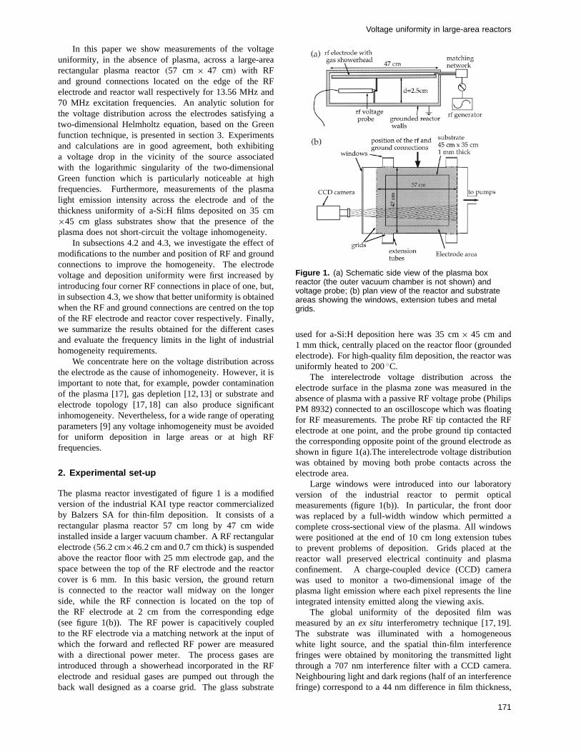
The plasma reactor investigated of figure 1 is a modifiedversion of the industrial KAI type reactor commercializedby Balzers SA for thin-film deposition. It consists of arectangular plasma reactor 57 cm long by 47 cm wideinstalled inside a larger vacuum chamber. A RF rectangularelectrode(56.2 cm×46.2 cm and 0.7 cm thick) is suspendedabove the reactor floor with 25 mm electrode gap, and thespace between the top of the RF electrode and the reactorcover is 6 mm. In this basic version, the ground returnis connected to the reactor wall midway on the longerside, while the RF connection is located on the top ofthe RF electrode at 2 cm from the corresponding edge(see figure 1(b)). The RF power is capacitively coupledto the RF electrode via a matching network at the input ofwhich the forward and reflected RF power are measuredwith a directional power meter. The process gases areintroduced through a showerhead incorporated in the RFelectrode and residual gases are pumped out through theback wall designed as a coarse grid. The glass substrate
Figure 1. (a) Schematic side view of the plasma boxreactor (the outer vacuum chamber is not shown) andvoltage probe; (b) plan view of the reactor and substrateareas showing the windows, extension tubes and metalgrids.
used for a-Si:H deposition here was 35 cm× 45 cm and1 mm thick, centrally placed on the reactor floor (groundedelectrode). For high-quality film deposition, the reactor wasuniformly heated to 200◦C.
The interelectrode voltage distribution across theelectrode surface in the plasma zone was measured in theabsence of plasma with a passive RF voltage probe (PhilipsPM 8932) connected to an oscilloscope which was floatingfor RF measurements. The probe RF tip contacted the RFelectrode at one point, and the probe ground tip contactedthe corresponding opposite point of the ground electrode asshown in figure 1(a).The interelectrode voltage distributionwas obtained by moving both probe contacts across theelectrode area.
Large windows were introduced into our laboratoryversion of the industrial reactor to permit opticalmeasurements (figure 1(b)). In particular, the front doorwas replaced by a full-width window which permitted acomplete cross-sectional view of the plasma. All windowswere positioned at the end of 10 cm long extension tubesto prevent problems of deposition. Grids placed at thereactor wall preserved electrical continuity and plasmaconfinement. A charge-coupled device (CCD) camerawas used to monitor a two-dimensional image of theplasma light emission where each pixel represents the lineintegrated intensity emitted along the viewing axis.
The global uniformity of the deposited film wasmeasured by anex situ interferometry technique [17, 19].The substrate was illuminated with a homogeneouswhite light source, and the spatial thin-film interferencefringes were obtained by monitoring the transmitted lightthrough a 707 nm interference filter with a CCD camera.Neighbouring light and dark regions (half of an interferencefringe) correspond to a 44 nm difference in film thickness,
171
L Sansonnens et al
taking the a-Si:H refractive index to be 4 [20]. Thedirection of the film thickness gradient, which is not givenby this global technique, was determined by means of asecondex situ interferometer system [17]. The transmittedwhite light was collected at a point with an optical fibreand analysed by a monochromator and optical multichannelanalyser. If the detection point was then moved acrossa region where the film became thicker, the interferenceextrema were displaced towards smaller wavelengths.
3. Theoretical model
3.1. Green’s function solutions
Rather than tackling our problem in the full geometricalcomplexity of figure 1, let us first consider the problem ofsolving Maxwell’s equations for a system composed of twoequal-sized, lossless, metallic plates which are positionedalong the (x, y) planes atz = ±d/2. Because of theplanar geometry and since the inter-electrode distanced
is assumed to be small compared to thex and y sizes,the electric fieldE = Ez(x,y)z can be taken to beperpendicular to the electrodes (no fringing effect) withEz constant along thez direction (homogeneous interstitialmedium). Assuming furthermore an exp(−iωt) timedependence, it can easily be shown [16] that Maxwell’sequations then reduce to a driven, two-dimensionalHelmholtz equation
(∇2+ k2)V (x) = iωµdJz(x) x = (x, y) ∈ � (1)
for the voltageV ≡ − ∫ dzEz = −Ezd between plates,where∇2 ≡ ∂2/∂x2+ ∂2/∂y2 and
k2 ≡ εµω2
(= ω2
c2in vacuum
)(2)
ε and µ being the permittivity and permeability,respectively, of the interstitial medium. The driving termin (1) is proportional to the current densityJz oscillatingat angular frequencyω. For simplicity, it is convenientto assume the source to be applied symmetrically on bothplates Jz(z = −d/2) = −Jz(z = d/2), though thegeneralization to asymmetric sources is straightforward. Inthe latter case,Jz should be regarded as the sum of theRF and ground electrode current densities with a negativesign associated with the bottom (ground) excitation. Weshall discuss for convenience only the voltage distributionoccurring on the top electrode (RF), keeping in mind thatthere exists this duality between RF and ground electrodes.
Equation (1) can be solved using the Green functionmethod [21]. Let the Green functiong(x;xs) satisfyingappropriate, homogeneous boundary conditions be asolution of the Helmholtz equation driven by a Dirac sourceat xs :
(∇2+ k2)g(x;xs) = δ(x− xs) xs ∈ �. (3)
Then, by virtue of the superposition principle, the totalsolution
V (x) =∫
d�s g(x;xs)s(xs) (4)
can be written as the sum of all responses to Dirac sources,weighted by the source distribution functions ≡ iωµdJz.
The Green function is generally not known, except inthe case of boundaries at infinity [21]. The asymptoticbehaviour of the Green function near theδ sourceis, however, well known from standard textbooks ondifferential equations. It can easily be obtained by surfaceintegration of (3) over a circular area of radiusR aboutthe Dirac source point. Since the Dirac source stronglyaffects the voltage gradient in the vicinity ofxs , the termproportional to k2 in (3) can be neglected providedRremains small. From the divergence theorem one then gets∂g(x,xs)/∂R ≈ 1/(2πR) or
g(x,xs)→ 1
2πln(R/R0) R ≡ |x− xs | (5)
asR → 0, whereR0 is a constant of integration. Thus,a pointlike connection produces a logarithmic voltagesingularity in two dimensions. A similar calculation in onedimension would show that the voltage remains boundedalthough the derivative is discontinuous at the source point.This emphasizes the importance of a full two-dimensionaldescription. Property (5) is essential to understand theexperimental and analytic results shown in section 4.
A closed form of the Green function can be obtainedfor simple geometries, i.e. when arbitrary functions can beexpanded
f (x) =∑n
fn8n(x) (6)
in a complete set of eigenfunctions8n(x),
(∇2+ k2)8n(x) = λn8n(x) (7)
satisfying appropriate, homogeneous boundary conditions.The Green function then reads [15, 16]
g(x;xs) =∑n
8n(x)8n(xs)
λn〈8n,8n〉 〈8n,8n〉 ≡∫
d�82n.
(8)
3.2. Boundary conditions and impedance discontinuity
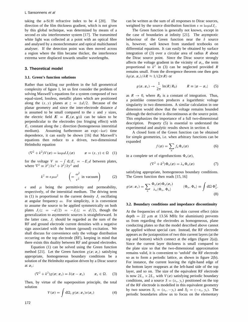
At the frequencies of interest, the skin current effect (skindepth= 22 µm at 13.56 MHz for aluminium) preventsus from regarding the electrodes as homogeneous, planeconducting plates so that the model described above cannotbe applied without special care. Instead, the RF electrodeappears as the juxtaposition of two thin current layers (at thetop and bottom) which connect at the edges (figure 2(a)).Since the current layer thickness is small compared tothe plate size so that the two-dimensional approximationremains valid, it is convenient to ‘unfold’ the RF electrodeso as to form a periodic lattice, as shown in figure 2(b).For instance, the current leaving the right-hand edge ofthe bottom layer reappears at the left-hand side of the toplayer, and so on. The size of the equivalent RF electrodeis now 2Lx × 2Ly with V (x) satisfying periodic boundaryconditions, and a sourceS = (xs, ys) positioned on the topof the RF electrode is modelled in this equivalent geometryby two sourcesS1 = (xs,−ys) and S2 = (−xs, ys). Theperiodic boundaries allow us to focus on the elementary
172
Voltage uniformity in large-area reactors
Figure 2. Schematic view of the RF electrode showing(a) the continuity of surface current flow and (b) anelementary cell in the unfolded two-dimensional geometryrepresentation.
Figure 3. Schematic one-dimensional representation of theimage source for the calculation of the (a) top and(b) bottom voltage distribution across the RF electrode inthe case where the top and bottom characteristicimpedances are different.
cell of figure 2(b) only. The eigenfunctions of (7) and (8)are therefore
8n = exp(iπ(nxx/Lx + nyy/Ly))2√LxLy
(9)
wheren = {nx, ny}, with 〈8n,8n′ 〉 = δn,n′ and λn =k2− π2n2
x/L2x − π2n2
y/L2y .
There is yet another complication to take into account,namely the fact that the distanced separating the RFelectrode from the ground electrode is different on the topand bottom. The characteristic impedanceZ scaling as∼d, the requirements of continuous voltage and current (orelectric and magnetic fields)
V |b = V |t
1
Zb
∂V
∂n
∣∣∣∣b
= 1
Zt
∂V
∂n
∣∣∣∣t
(10)
across the bottom–top interface, can generally only beachieved with a discontinuous normal derivative∂V/∂n atthe interfaces (edges). There is however a simple way toconstruct, by linear combination, aV (x) solution which:(a) satisfies (1), (b) has periodic boundary conditions and(c) possesses the derivative discontinuity according to (10).To be more specific, let us assume, as it is the case in theexperimental set-up, that the RF connection is modelled bya δ function that is located on the top layer. The sourcewill radiate8n waves but some will bounce back due toreflections occurring at the interface. For an observer on thetop layer, there is no way to discriminate between reflectedwaves and those emitted by a mirror source on the bottomlayer (analogous the image method in electrostatics, seefigure 3). It is not difficult to prove that the amplitude of theimage source must be(Zb −Zt)/(Zb +Zt), that is exactlythe reflection coefficient. In the case where the top andbottom sizes are identical, one can verify that reflectionsat the boundaries of the elementary cell do not introduceadditional image sources. In the limit ofZb → 0, theimage source has the same but opposite amplitude whereasthe image source amplitude is equal to the source amplitudein the Zb → ∞ limit. Homogeneous Dirichlet boundaryconditions apply at the top edge in the former case whereashomogeneous Neumann boundary conditions apply in thesecond one.
A solution on the bottom side can then be constructedby multiplying the source by the transmission coefficient2Zb/(Zb + Zt). Hence, the impedance discontinuity willnot affect the behaviour of the solution on the bottom layer,merely introducing a multiplicative coefficient. This incontrast to the top layer where the source is located andwhere the behaviour ofV is modified by reflections.
3.3. Standing wave and finite area connector
We are now able to identify two distinct regimes ofvoltage inhomogeneity. The first is the regime whereinhomogeneity is dominated by the logarithmic singularity(5) of a pointlike connection. A large number ofFourier components are required to correctly representthis singularity. Clearly this regime can only take placeoff resonance. The second is the standing wave regimeobtained whenλn = 0 in (8) and only one Fourier modesurvives. The voltage inhomogeneity then results from thedifference of amplitude between an antinode and a nodethrough the parameterk. Since we allownx andny to varyas 0, 1, 2, . . . , the lowest resonance is atk2 = 0, yieldinga flat voltage distribution.
These two regimes are best illustrated in figure 4 fortwo types of source: an edge line sources = δ(x) ((a) and(b)) and an edge point sources = δ(x)δ(y−Ly/2) ((c) and(d)), at two frequenciesf = 150 MHz (left) and 300 MHz(right). In figure 4(a) we have chosen the wavelengthλ ≈ Lx/4; the problem becomes one dimensional in thiscase due to the choice of the line source with the voltageremaining bounded in contrast to case (c) where the sourceis peaked. The main source of voltage inhomogeneity at
173

L Sansonnens et al
Figure 4. Voltage distribution normalized to the maximumvalue for two different frequencies: f = 150 MHz (cases (a)and (c)) and 300 MHz ((b) and (d)). The source distributions = δ(x) is taken to be uniform along the x = 0 axis forcases (a) and (b), but is pointlike s = δ(x)δ(y − Ly/2) forcases (c) and (d). The electrode size is 47 cm× 57 cm.
f = 150 MHz for a pointlike source is the logarithmicsingularity (case (c)). As the frequency increases tof =300 MHz we approach the (nx = 1, ny = 0) resonance.The one-dimensional (b) and two-dimensional (d) cases arequalitatively similar because of the negligible role played bythe source. The singular source effects reappear at higherfrequencies but their coupling to resonant, standing waveinhomogeneities becomes more effective due to the higherdensity of resonances in this part of the spectrum (resultsnot shown).
It may be appropriate to comment at this point on thefinite-size effect of a source. If we replace theδ function bya source which is zero everywhere except on an areaπa2
where its amplitude is constant and inversely proportional tothe area (a crude approximation ofδ(x)), one then recoversthe logarithmic function (5) outside the radiusa, whereas∂g(x,xs)/∂R ≈ R/(2πa2) inside it. The replacement ofa finite-sized source by a Dirac function in the simulationsis therefore valid outside the contact area.
4. Results
4.1. Electrode with a single edge connection
Figure 5 shows the measured and calculated RF voltageamplitude distributions across the electrode for twofrequencies. The measurements were performed withoutplasma as described in section 2, and the calculations weremade with the model developed in subsection 3.1. TheRF and ground return connections were located midwayalong the long edge of the RF electrode and ground reactorwall respectively as described in section 2. This position isindicated by the black point on the figure axis.
At 13.56 MHz, the measured voltage amplitude isalmost constant across the whole electrode area, whereasat 70 MHz, it is highly non-uniform in the vicinity ofthe RF connection. This observed non-uniformity is well
Figure 5. (a) Normalized measurements and(b) calculations of the interelectrode voltage distributionover the electrode area in the absence of plasma for13.56 MHz and 70 MHz frequencies. The black pointindicates the position of the RF and ground connections.
Figure 6. Emission intensity profile of an argon plasma(55 W RF power, 0.1 Torr pressure) across the frontfull-width window for three frequencies. The intensity isintegrated across the electrode gap and normalized to themaximum intensity. The position 0 cm corresponds to theside of the reactor where the RF is connected.
described by the logarithmic singularity due to a localsource as predicted in the two-dimensional model andcannot be described by a one-dimensional model. Thevoltage inhomogeneity1v can be defined by the expression:
±1v ≡ Vmax − VminVmax + Vmin (11)
where Vmax and Vmin are respectively the maximumand minimum peak-to-peak voltages measured over theelectrode area. Although (11) is experimentally convenient,we are conscious that this expression becomes formallyone for a pointlike connector due to the singularity of thevoltage but in reality, the finite contact area of the RFconnector smears out the singularity. We find1v = ±0.5%at 13.56 MHz while1v = ±30% at 70 MHz. These resultsshow that an increase in the RF frequency strongly increasesthe voltage inhomogeneity across the electrode.
174
Voltage uniformity in large-area reactors
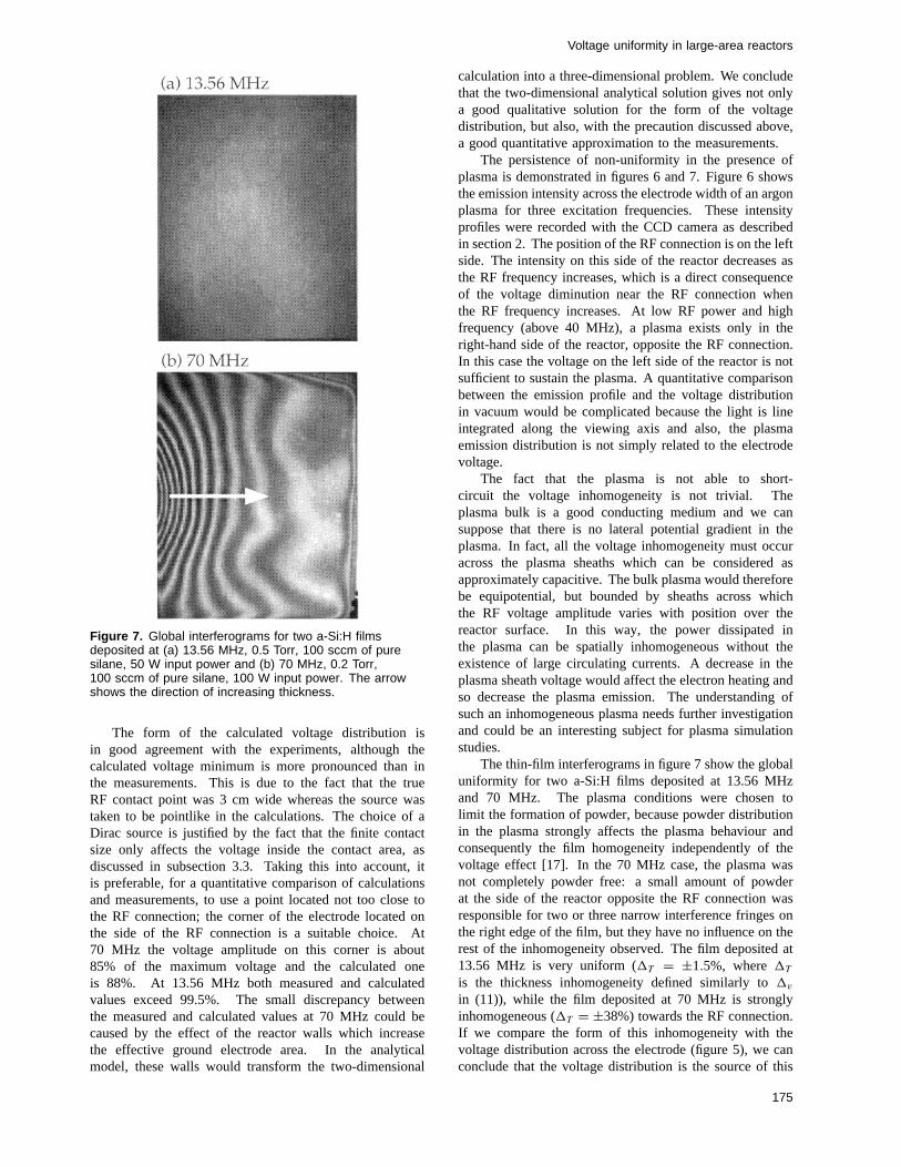
Figure 7. Global interferograms for two a-Si:H filmsdeposited at (a) 13.56 MHz, 0.5 Torr, 100 sccm of puresilane, 50 W input power and (b) 70 MHz, 0.2 Torr,100 sccm of pure silane, 100 W input power. The arrowshows the direction of increasing thickness.
The form of the calculated voltage distribution isin good agreement with the experiments, although thecalculated voltage minimum is more pronounced than inthe measurements. This is due to the fact that the trueRF contact point was 3 cm wide whereas the source wastaken to be pointlike in the calculations. The choice of aDirac source is justified by the fact that the finite contactsize only affects the voltage inside the contact area, asdiscussed in subsection 3.3. Taking this into account, itis preferable, for a quantitative comparison of calculationsand measurements, to use a point located not too close tothe RF connection; the corner of the electrode located onthe side of the RF connection is a suitable choice. At70 MHz the voltage amplitude on this corner is about85% of the maximum voltage and the calculated oneis 88%. At 13.56 MHz both measured and calculatedvalues exceed 99.5%. The small discrepancy betweenthe measured and calculated values at 70 MHz could becaused by the effect of the reactor walls which increasethe effective ground electrode area. In the analyticalmodel, these walls would transform the two-dimensional
calculation into a three-dimensional problem. We concludethat the two-dimensional analytical solution gives not onlya good qualitative solution for the form of the voltagedistribution, but also, with the precaution discussed above,a good quantitative approximation to the measurements.
The persistence of non-uniformity in the presence ofplasma is demonstrated in figures 6 and 7. Figure 6 showsthe emission intensity across the electrode width of an argonplasma for three excitation frequencies. These intensityprofiles were recorded with the CCD camera as describedin section 2. The position of the RF connection is on the leftside. The intensity on this side of the reactor decreases asthe RF frequency increases, which is a direct consequenceof the voltage diminution near the RF connection whenthe RF frequency increases. At low RF power and highfrequency (above 40 MHz), a plasma exists only in theright-hand side of the reactor, opposite the RF connection.In this case the voltage on the left side of the reactor is notsufficient to sustain the plasma. A quantitative comparisonbetween the emission profile and the voltage distributionin vacuum would be complicated because the light is lineintegrated along the viewing axis and also, the plasmaemission distribution is not simply related to the electrodevoltage.
The fact that the plasma is not able to short-circuit the voltage inhomogeneity is not trivial. Theplasma bulk is a good conducting medium and we cansuppose that there is no lateral potential gradient in theplasma. In fact, all the voltage inhomogeneity must occuracross the plasma sheaths which can be considered asapproximately capacitive. The bulk plasma would thereforebe equipotential, but bounded by sheaths across whichthe RF voltage amplitude varies with position over thereactor surface. In this way, the power dissipated inthe plasma can be spatially inhomogeneous without theexistence of large circulating currents. A decrease in theplasma sheath voltage would affect the electron heating andso decrease the plasma emission. The understanding ofsuch an inhomogeneous plasma needs further investigationand could be an interesting subject for plasma simulationstudies.
The thin-film interferograms in figure 7 show the globaluniformity for two a-Si:H films deposited at 13.56 MHzand 70 MHz. The plasma conditions were chosen tolimit the formation of powder, because powder distributionin the plasma strongly affects the plasma behaviour andconsequently the film homogeneity independently of thevoltage effect [17]. In the 70 MHz case, the plasma wasnot completely powder free: a small amount of powderat the side of the reactor opposite the RF connection wasresponsible for two or three narrow interference fringes onthe right edge of the film, but they have no influence on therest of the inhomogeneity observed. The film deposited at13.56 MHz is very uniform (1T = ±1.5%, where1T
is the thickness inhomogeneity defined similarly to1v
in (11)), while the film deposited at 70 MHz is stronglyinhomogeneous (1T = ±38%) towards the RF connection.If we compare the form of this inhomogeneity with thevoltage distribution across the electrode (figure 5), we canconclude that the voltage distribution is the source of this
175
L Sansonnens et al
Figure 8. Dependence of the film thickness at 70 MHz onthe square of the measured voltage.
inhomogeneity. This is an additional demonstration that theplasma is strongly affected by the voltage distribution.
The inhomogeneity in the 70 MHz deposited filmindicates that the diffusion path of the reactive species mustbe short (<3 cm) since a long diffusion path would tendto average out the deposition rate across the substrate area.This point is also confirmed by the fact that no deposition isobserved on the windows located at the end of the extensiontubes (figure 1).
Figure 8 shows an approximate linear relation betweenthe film thickness and the square of the voltage measuredwithout plasma at the same point for the 70 MHz case. Thethickness data were taken from figure 7(b) and the voltagedata from figure 5(a). For a silane plasma without powder,a linear relation is generally observed between the square ofthe peak-to-peak voltage measured during the plasma andthe input power into the reactor [22]. Assuming that theplasma does not affect the form of the voltage distributionacross the electrode, figure 8 therefore indicates that thelocal deposition rate is roughly proportional to the localdissipated power.
4.2. Multi-source case
The results and calculations presented in the precedingsection show that a single RF connection at the electrodeedge does not satisfy the homogeneity requirement forindustrial applications when operating in the VHF range.A similar limitation would also be found at 13.56 MHz ifthe size of the electrode were increased. A possible wayto improve the uniformity, as also shown by Kuskeet al[14], is to increase the number of RF power connections.Figure 9 shows such a modification applied to our reactor:the single RF connection is replaced by four connectionslocated near the corners on the top of the RF electrode,while the ground return connection remains located midwayon the longer side wall of the reactor. These RF and groundconnection positions were not the result of a study but ratherof the practical restrictions imposed by the electrode design.
Figure 10 shows the measurement and the calculation ofthe interelectrode voltage distribution across this modifiedelectrode for 70 MHz frequency. The amplitudes of theRF current sources are each a quarter of the amplitudeof the ground return current to conserve the total current.The measurements show that the inhomogeneity is partially
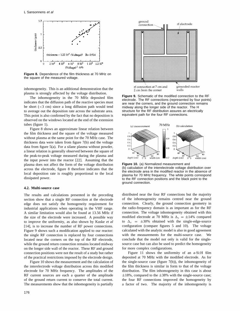
Figure 9. Schematic of the modified connection to the RFelectrode. The RF connections (represented by four points)are near the corners, and the ground connection remainsmidway along the longer side of the reactor. The Hstructure for the RF distribution assures an electricallyequivalent path for the four RF connections.
Figure 10. (a) Normalized measurement and(b) calculation of the interelectrode voltage distribution overthe electrode area in the modified reactor in the absence ofplasma for 70 MHz frequency. The white points correspondto the RF connection positions and the black point to theground connection.
distributed near the four RF connections but the majorityof the inhomogeneity remains centred near the groundconnection. Clearly, the ground connection geometry inthe radio-frequency domain is as important as for the RFconnection. The voltage inhomogeneity obtained with thismodified electrode at 70 MHz is1v = ±14% comparedto 1v = ±30% obtained with the single-edge-sourceconfiguration (compare figures 5 and 10). The voltagecalculated with the analytic model is also in good agreementwith the measurements for the multi-source case. Weconclude that the model not only is valid for the single-source case but can also be used to predict the homogeneityfor more complex configurations.
Figure 11 shows the uniformity of an a-Si:H filmdeposited at 70 MHz with the modified electrode. As forthe single-source case (figure 7(b)), the inhomogeneity ofthe film thickness is similar in form to that of the voltagedistribution. The film inhomogeneity in this case is about±18%, compared to the±38% with the single-source case;the four RF connections improved the homogeneity bya factor of two. The majority of the inhomogeneity is
176

Voltage uniformity in large-area reactors
Figure 11. Global interferogram for an a-Si:H filmdeposited at 70 MHz, 0.2 Torr, 100 sccm of pure silane and100 W input power, using the modified RF electrode. Thearrows show the direction of increasing thickness.
Figure 12. (a) Normalized measurement and(b) calculation of the interelectrode voltage distribution overthe electrode area in the absence of plasma for one RFand one ground connection centred on the top of the RFelectrode and reactor cover respectively for 70 MHzfrequency. The white points correspond to the RF andground connection positions.
caused by the return ground connection. Using the analyticmodel, we show below (in figure 13) that if four groundconnections were used as for the RF connections, thisinhomogeneity would be further reduced.
4.3. Electrode with a single centred connection
The results obtained in subsections 4.1 and 4.2 have shownthat the majority of the voltage distribution inhomogeneityis located in the vicinity of the connections. When theconnections are located on the edge of the reactor, thisdrastically decreases the film thickness homogeneity. Insubsection 4.2, a better homogeneity was obtained byincreasing the number of RF connections on the edge of theRF electrode. Another way to increase the homogeneityis to move the RF and ground connections to the centreof the top of the RF electrode and of the reactor coverrespectively. Due to the skin effect of the currentpropagation, this configuration maximizes the distancebetween the source and the plasma zone. Figure 12 shows
Figure 13. Dependence on the RF frequency of (a) thevoltage inhomogeneity 1v in the absence of plasma and(b) the film thickness inhomogeneity 1T , both evaluated forthe substrate area. The lines correspond to calculatedvalues and the points to the experimental measurements.The configurations are: (i) one RF and one groundconnection midway along the long side of the reactor(subsection 4.1); (ii) four RF connections near the cornersof the electrode and one ground connection midway alongthe long side of the reactor (subsection 4.2); (iii) four RFand four ground connections near the corners of theelectrode (at the same location as in (ii)); (iv) one RF andone ground connection centred on the top of the RFelectrode and reactor (subsection 4.3).
the measured and the calculated voltage distribution acrossthe electrode obtained in this configuration for 70 MHzfrequency. As expected, the singularity associated with thesource does not affect the voltage in the plasma zone, andthe voltage inhomogeneity obtained in this case is1v =±3%. The good correspondence between measurementsand calculations in this case shows the ability of the modelto describe configurations with connections not only locatedon the edge of the reactor or RF electrode.
5. Discussion and conclusions
Figure 13 presents the voltage and the film thicknessinhomogeneity across the substrate area(35 cm× 45 cm)for four different connection geometries. The thicknessinhomogeneity is calculated from the voltage distributionby using the linear relation between the square of thepotential and the deposition rate from figure 8. It is clearthat the thickness inhomogeneity predicted here is onlyvalid for plasma conditions where this linear relation isverified. Other conditions such as plasma with powdercontamination [17], gas depletion [12, 13] or substrateand electrode topology [17, 18] can also influence thehomogeneity. Nevertheless, for a wide range of operatingparameters any voltage inhomogeneity must be avoided foruniform deposition in large areas or at high RF frequencies.
177

L Sansonnens et al
The close agreement between experiment and calcula-tion shows that the model can be used to predict and opti-mize the RF and ground connection scheme. It appears thatVHF operation in the actual modified electrode (case (ii)) islimited to 55 MHz for the solar cell homogeneity require-ment (±10%) and to 40 MHz for the flat panel displayrequirement (±5%). This limit would be raised to 80 MHzfor solar cells and 60 MHz for flat panels if the ground con-nection were also divided into four connections (case (iii)).However better results are expected for a single RF andground connection centred on the top of RF electrode andreactor cover; the estimated limitation would be 85 MHzfor flat panels and more than 100 MHz for solar cells. Inall cases, 13.56 MHz operation is sufficiently homogeneousfor flat panel applications.
Since the advantages of VHF operation have beendemonstrated in small-area reactors [1], upscaling to largesurfaces must be done by taking special care over the designof the RF and ground connections to achieve the homogene-ity required for industrial applications. Finally, we note thepotential for specially designed profiles of the film thicknessby controlling the plasma power deposition uniformity viathe RF frequency and connection geometry. In all cases,prediction for the design of a reactor could be made byusing the two-dimensional model presented in this paper.
Acknowledgments
We thank the IMT Neuchatel group of Professor Shahfor useful discussions and encouragement, and L Gabellaand J Redondo for assistance in computer modelling.This work was funded by Swiss Federal Research GrantBEW 9400051 and partly supported by the Swiss NationalFoundation.
References
[1] Curtins H, Wyrsch N, Favre M and Shah A 1987PlasmaChem. Plasma Processing7 267
[2] Howling A A, Dorier J-L, Hollenstein C, Kroll U andFinger F 1992J. Vac. Sci. Technol.A 10 1080
[3] Colgan M J, Meyyappan M and Murnick D E 1994PlasmaSources Sci. Technol.3 181
[4] Heintze M, Zedlitz R and Bauer G H 1993J. Phys. D:Appl. Phys.26 1781
[5] Keppner H, Kroll U, Meyer J and Shah A 1995Solid StatePhenom.44 97
[6] Finger F, Kroll U, Viret V, Shah A, Beyer W, Tang X-M,Weber J, Howling A A and Hollenstein C 1992J. Appl.Phys.71 5665
[7] Meiling H, Westendorp J F M, Hautala J, Saleh Z M andMalone C T 1994Mater. Res. Soc. Symp. Proc.vol 345(Pittsburgh, PA: Materials Research Society) p 65
[8] Westendorp J F M, Meiling H, Pollock J D, Berrian D W,Laflamme A H, Hautala J and Vanderpot J 1994Mater.Res. Soc. Symp. Proc.vol 345 (Pittsburgh, PA: MaterialsResearch Society) p 175
[9] Van Sark W G J H M,Bezemer J, Heller E M B, Kars Mand Van der Weg W F 1995Mater. Res. Soc. Symp.Proc. vol 377 (Pittsburgh, PA: Materials ResearchSociety) p 3
[10] Surendra M and Graves D B 1991Appl. Phys. Lett.592091
[11] Vahedi V, Birdsall C K, Liebermann M A, DiPeso G andRognlien T D 1993Phys. FluidsB 5 2719
[12] Schmitt J P M 1989Thin Solid Films174 193[13] Schmitt J P M 1992Mat. Res. Soc. Symp. Proc.vol 219
(Pittsburgh, PA: Materials Research Society) p 631[14] Kuske J, Stephan U, Steinke O and Rhlecke S 1995Mat.
Res. Soc. Symp. Proc.vol 377 (Pittsburgh, PA: MaterialsResearch Society) p 27
[15] Okoshi T and Miyoshi T 1972IEEE Trans. MicrowaveTheory Technol.MTT-20 245
[16] Sorrentino R 1985IEEE Trans. Microwave Theory Technol.MTT-33 431
[17] Sansonnens L, Franz D, Hollenstein C, Howling A A,Schmitt J P M, Turlot E, Emeraud T, Kroll U, Meyer Jand Shah A 1995Proc. 13th EC Photovoltaic SolarEnergy Conf.p 319
[18] Meiling H, Van Sark W G J H M, Bezemer J and Van derWeg W F 1996J. Appl. Phys.80 3546
[19] Solomon I, Bhatnagar M and Rosso M 1991Proc. 10th ECPhotovoltaic Solar Energy Conf.p 154
[20] Forouhi A R 1989 Properties of Amorphous Silicon(INSPEC, Institute of Electrical Engineers) p 337
[21] Morse P M and Feshbach H 1953Methods of TheoreticalPhysics(New York: MacGraw-Hill) p 891
[22] Dorier J-L, Hollenstein C and Howling A A 1992 J. Vac.Sci. Technol.A 10 1048
178