Embed Size (px)
Citation preview
A REVIEW ON MEMRISTOR APPLICATIONS
Roberto Marani, Gennaro Gelao and Anna Gina Perri
Electronic Devices Laboratory, Electrical and Information Engineering Department,
Polytechnic University of Bari, via E. Orabona 4, Bari – Italy [email protected]
ABSTRACT
This article presents a review on the main applications of the fourth fundamental circuit element, named
"memristor", which had been proposed for the first time by Leon Chua and has recently been developed by a
team at HP Laboratories led by Stanley Williams. In particular, after a brief analysis of memristor theory with a
description of the first memristor, manufactured at HP Laboratories, we present its main applications in the
circuit design and computer technology, together with future developments.
KEYWORDS
Memristor, Modelling, P-SPICE, Memristor Applications.
1. INTRODUCTION
Memristor, a concatenation of “memory resistor”, is a type of passive circuit element that maintains a
relationship between the time integrals of current and voltage across a two terminal element. In fact its
resistance depends on the charge that flowed through the circuit. When current flows in one direction
the resistance increases, in contrast when the current flows in opposite direction the resistance
decreases. However resistance cannot go below zero. When the current is stopped, the resistance
remains in the value that it had earlier.
It means that memristor “remembers” the current that last flowed through it.
In this paper we analyze the memristor theory. In particular a description of the first memristor,
manufactured at HP Laboratories, is presented with its implementation in P-SPICE simulator. Finally
we highlight its main applications in the circuit design and computer technology.
The presentation is organized as follows. Section 2 gives a brief description of memristor theory. The
HP Memristor and its implementation in P-SPICE simulator is presented in Section 3, while the
description of the main current applications of memristor is given in section 4. The conclusions and
future developments are described in Section 5.
2. MEMRISTOR THEORY
Passive circuit theory can be thought of as a set of relationships between electromagnetic quantities:
1) Voltage v, defined as the change magnetic flux Φ with respect to time t;
2) Current i, defined as the change in electric charge q with respect to time;
3) Resistor R, defined as a linear relationship between voltage and current (dv = Rdi );
4) Capacitor C, defined as a linear relationship between voltage and electric charge (dq = Cdv);
5) Inductor L, defined as a linear relationship between magnetic flux Φ and current i (dΦ = Ldi).
Of the six possible relationships, the only two electromagnetic quantities for which there are no
pairings are magnetic flux and electric charge. However, in 1971 Leon Chua [1] hypothesized that
mathematically, a fourth fundamental passive circuit element could exist, proposing the fourth
component, called memristor, that binds the charge q to the linkage flux Φ (see Fig. 1, in which the
electrical symbol of memristor is also indicated):
dΦ= Mdq (1)
Figure 1. Memristor relationship (figure adapted from Nature).
In particular the memristor has originally been defined in terms of a non-linear functional relationship
between the so-called flux linkage φ(t) and the amount of electric charge that has flowed through the
device, q(t):
f(φ(t),q(t)) = 0 (2)
where φ(t) and q are time-domain integrals of memristor electric voltage v and electric current i,
respectively:
∫ ∞ττ=ϕ
t
- )dv( )t(
(3)
and
∫ ∞ττ=
t
- )di( )t(q (4)
The variable flux linkage φ(t) is generalized from the circuit characteristic of an inductor, and does
not represent a magnetic field here.
In Eq. (2) the derivative of one respect to the other depends on the value of one or the other.
In this way a memristor is characterized by its memristance function, which describes the charge-
dependent rate of change of flux with charge:
dq
d )q(M
ϕ= (5)
Introducing Eq, (3) in Eq, (5), we have:
)q(R
dt
dqdt
d
))t(q(M M=
ϕ
= (6)
where RM(q) is the small-signal memristance defined in the operating point. In this way we have a
charge-controlled or current-controlled memristor.
Analogously, introducing Eq, (4) in (5), we have:
)(G
dt
ddt
dq
))t((M M ϕ=ϕ
=ϕ (7)
obtaining, in this way, a flux-controlled or voltage-controlled memristor.
The current-controlled memristor can be modeled via a classical resistor whose resistance is
controlled by the time-domain integral of the current flowing through the memristor. Analogously,
the voltage-controlled memristor behaves as a conductor whose conductance depends on the time-
domain integral of terminal voltage.
In both cases, we need an electronically controlled resistor/conductor and an integrator.
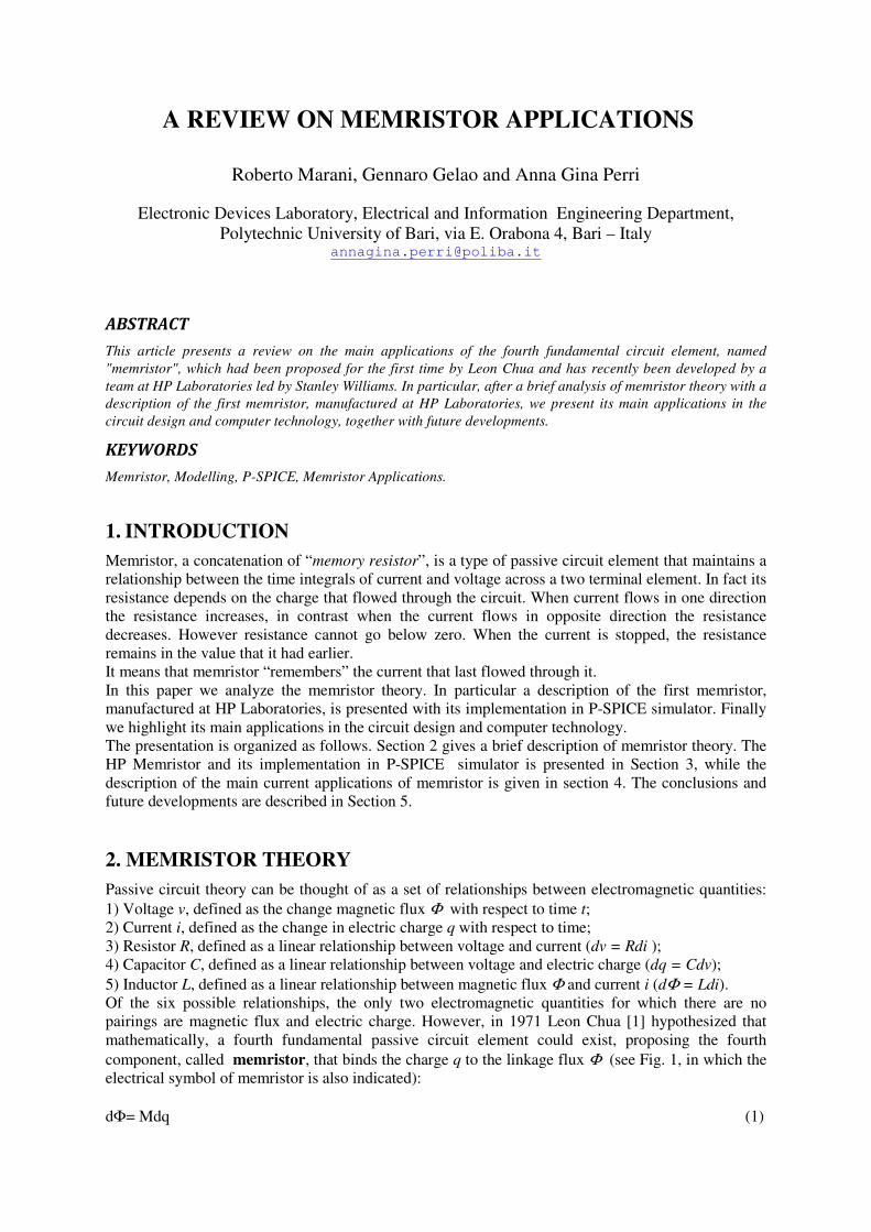
Table 1 covers all meaningful ratios of differentials of i, q, ϕ and v, while Fig. 2 shows the current-
voltage characteristics for memristor, where you can easily notice its fundamental identifier, i.e. its
pinched hysteresis loop.
Table 1
Device Units Differential Equation Resistor Ohm R = dv/di Capacitor Farad C = dq/dv Inductor Henry L = dϕ/di Memristor Ohm M = dϕ/dq
Figure 2. Current-voltage characteristics of a memristor.
With reference to Eq, (6), which can be written also in the following way;
v(t)= M(q(t)) i(t) (8)
if i(t) = 0, we find v(t) = 0 and therefore M(t) is constant (memory effect).
The power consumption characteristic recalls that of a resistor:
P(t) = V(t) I(t) = I2(t) M(q(t)) (9)
As long as M(q(t)) varies little, such as under alternating current, the memristor will appear as a
constant resistor.
When M(q(t)) increases rapidly, however, current and power consumption will quickly stop.
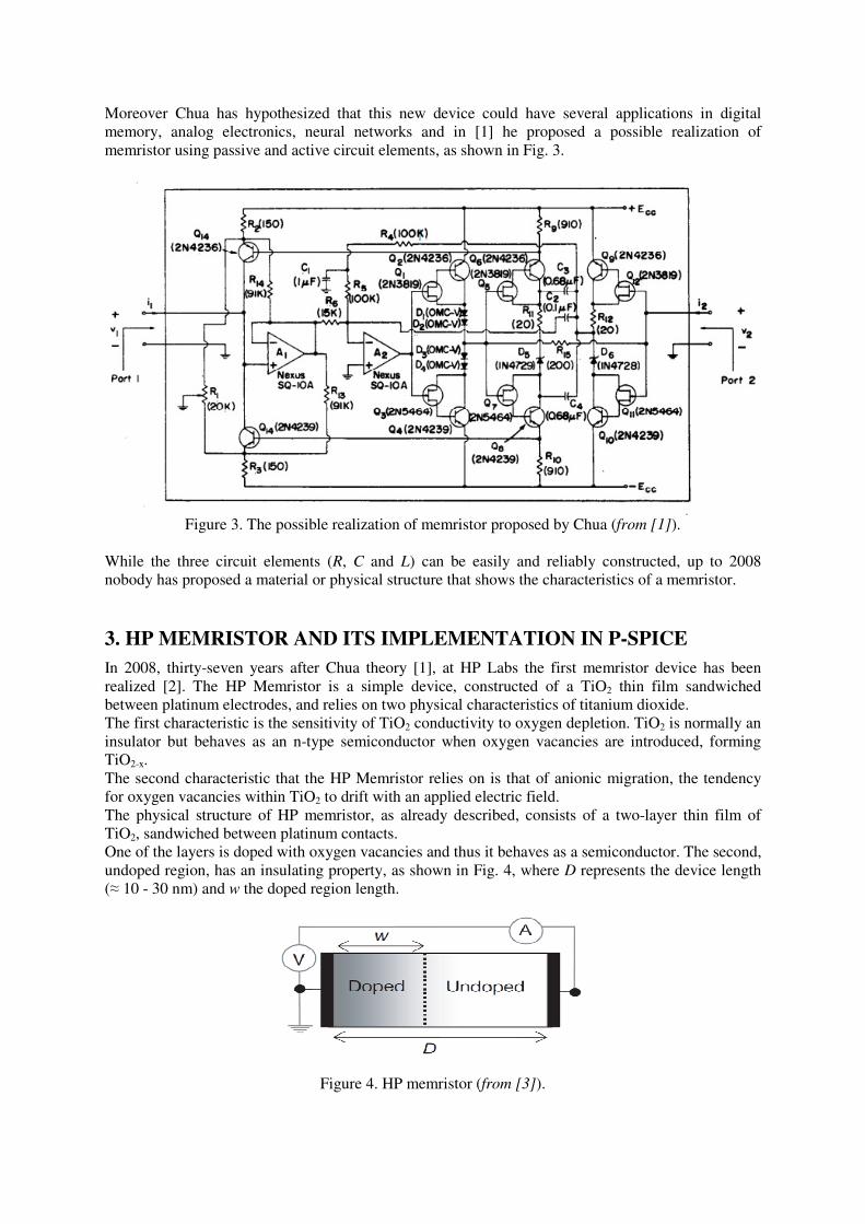
Moreover Chua has hypothesized that this new device could have several applications in digital
memory, analog electronics, neural networks and in [1] he proposed a possible realization of
memristor using passive and active circuit elements, as shown in Fig. 3.
Figure 3. The possible realization of memristor proposed by Chua (from [1]).
While the three circuit elements (R, C and L) can be easily and reliably constructed, up to 2008
nobody has proposed a material or physical structure that shows the characteristics of a memristor.
3. HP MEMRISTOR AND ITS IMPLEMENTATION IN P-SPICE
In 2008, thirty-seven years after Chua theory [1], at HP Labs the first memristor device has been
realized [2]. The HP Memristor is a simple device, constructed of a TiO2 thin film sandwiched
between platinum electrodes, and relies on two physical characteristics of titanium dioxide.
The first characteristic is the sensitivity of TiO2 conductivity to oxygen depletion. TiO2 is normally an
insulator but behaves as an n-type semiconductor when oxygen vacancies are introduced, forming
TiO2-x.
The second characteristic that the HP Memristor relies on is that of anionic migration, the tendency
for oxygen vacancies within TiO2 to drift with an applied electric field.
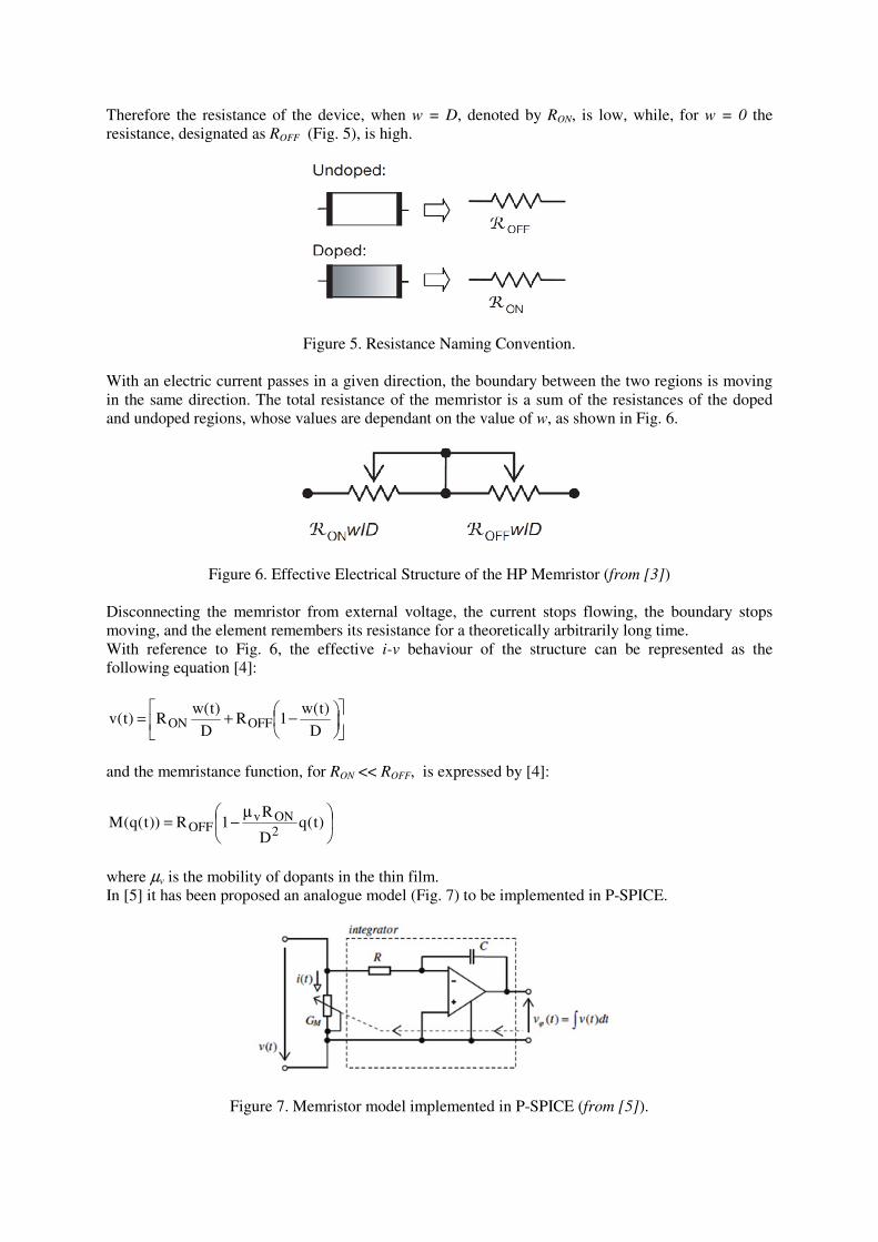
The physical structure of HP memristor, as already described, consists of a two-layer thin film of
TiO2, sandwiched between platinum contacts.
One of the layers is doped with oxygen vacancies and thus it behaves as a semiconductor. The second,
undoped region, has an insulating property, as shown in Fig. 4, where D represents the device length
(≈ 10 - 30 nm) and w the doped region length.
Figure 4. HP memristor (from [3]).
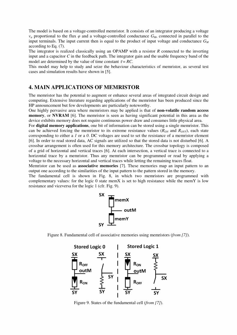
Therefore the resistance of the device, when w = D, denoted by RON, is low, while, for w = 0 the
resistance, designated as ROFF (Fig. 5), is high.
Figure 5. Resistance Naming Convention.
With an electric current passes in a given direction, the boundary between the two regions is moving
in the same direction. The total resistance of the memristor is a sum of the resistances of the doped
and undoped regions, whose values are dependant on the value of w, as shown in Fig. 6.
Figure 6. Effective Electrical Structure of the HP Memristor (from [3])
Disconnecting the memristor from external voltage, the current stops flowing, the boundary stops
moving, and the element remembers its resistance for a theoretically arbitrarily long time.
With reference to Fig. 6, the effective i-v behaviour of the structure can be represented as the
following equation [4]:
−+=
D
)t(w1R
D
)t(wR)t(v OFFON
and the memristance function, for RON << ROFF, is expressed by [4]:
µ−= )t(q
D
R1 R))t(q(M
2ONv
OFF
where µv is the mobility of dopants in the thin film.
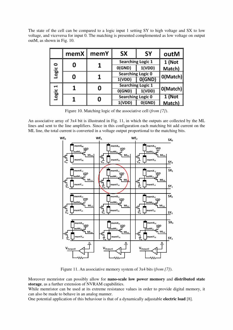
In [5] it has been proposed an analogue model (Fig. 7) to be implemented in P-SPICE.
Figure 7. Memristor model implemented in P-SPICE (from [5]).
The model is based on a voltage-controlled memristor. It consists of an integrator producing a voltage
vφ proportional to the flux φ and a voltage-controlled conductance GM, connected in parallel to the
input terminals. The input current then is equal to the product of input voltage and conductance GM
according to Eq. (7).
The integrator is realized classically using an OPAMP with a resistor R connected to the inverting
input and a capacitor C in the feedback path. The integrator gain and the usable frequency band of the
model are determined by the value of time constant τ = RC.
This model may help to study and seize the behaviour characteristics of memristor, as several test
cases and simulation results have shown in [5].
4. MAIN APPLICATIONS OF MEMRISTOR
The memristor has the potential to augment or enhance several areas of integrated circuit design and
computing. Extensive literature regarding applications of the memristor has been produced since the
HP announcement but few developments are particularly noteworthy.
One highly pervasive area where memristors may be applied is that of non-volatile random access
memory, or NVRAM [6]. The memristor is seen as having significant potential in this area as the
device exhibits memory does not require continuous power draw and consumes little physical area.
For digital memory applications, one bit of information can be stored using a single memristor. This
can be achieved forcing the memristor to its extreme resistance values (RON and ROFF), each state
corresponding to either a 1 or a 0. DC voltages are used to set the resistance of a memristor element
[6]. In order to read stored data, AC signals are utilized so that the stored data is not disturbed [6]. A
crossbar arrangement is often used for this memory architecture. The crossbar topology is composed
of a grid of horizontal and vertical traces [6]. At each intersection, a vertical trace is connected to a
horizontal trace by a memristor. Thus any memristor can be programmed or read by applying a
voltage to the necessary horizontal and vertical traces while letting the remaining traces float.
Memristor can be used as associative memories [7]. These memories map an input pattern to an
output one according to the similarities of the input pattern to the pattern stored in the memory.
The fundamental cell is shown in Fig. 8, in which two memristors are programmed with
complementary values: for the logic 0 state memX is set to high resistance while the memY is low
resistance and viceversa for the logic 1 (cfr. Fig. 9).
Figure 8. Fundamental cell of associative memories using memristors (from [7]).
Figure 9. States of the fundamental cell (from [7]).
The state of the cell can be compared to a logic input 1 setting SY to high voltage and SX to low
voltage, and viceversa for input 0. The matching is presented complemented as low voltage on output
outM, as shown in Fig. 10.
Figure 10. Matching logic of the associative cell (from [7]).
An associative array of 3x4 bit is illustrated in Fig. 11, in which the outputs are collected by the ML
lines and sent to the line amplifiers. Since in this configuration each matching bit add current on the
ML line, the total current is converted in a voltage output proportional to the matching bits.
Figure 11. An associative memory system of 3x4 bits (from [7]).
Moreover memristor can possibly allow for nano-scale low power memory and distributed state
storage, as a further extension of NVRAM capabilities.
While memristor can be used at its extreme resistance values in order to provide digital memory, it
can also be made to behave in an analog manner.
One potential application of this behaviour is that of a dynamically adjustable electric load [8].
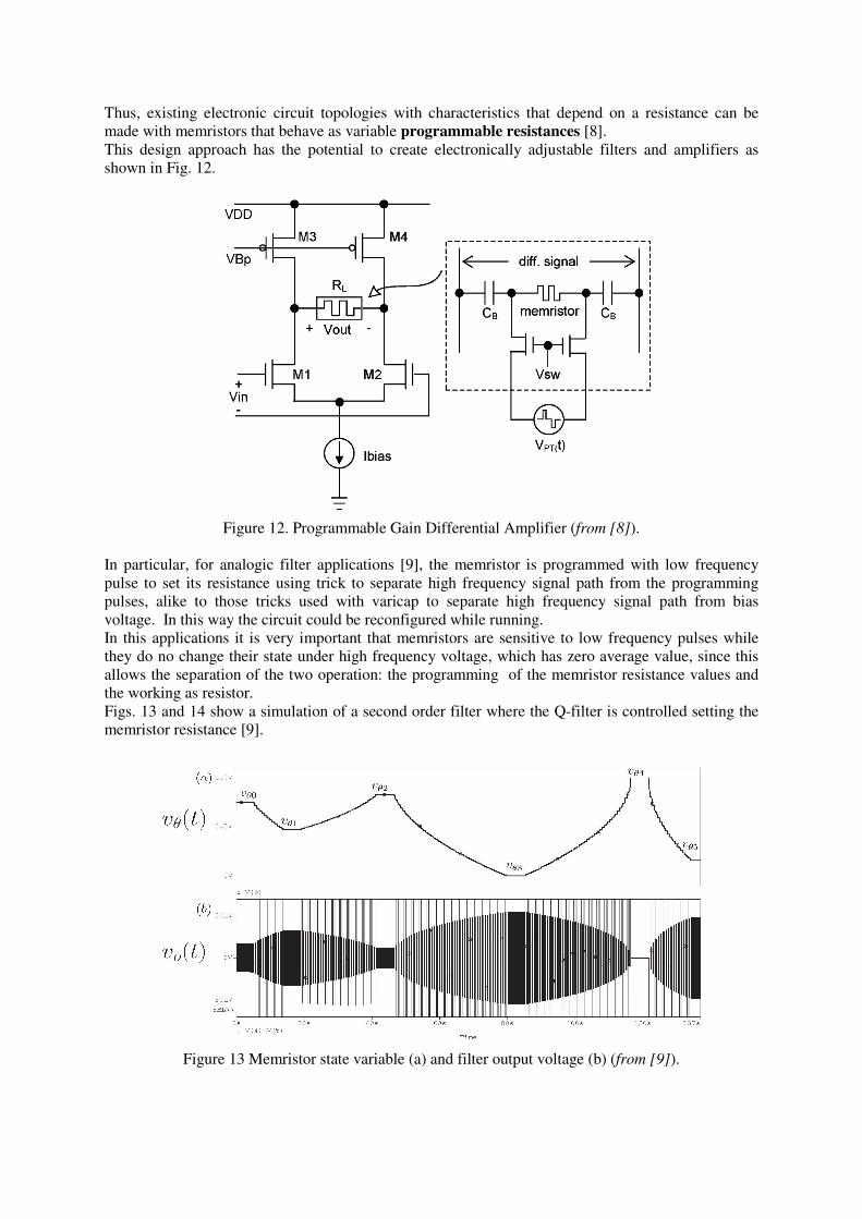
Thus, existing electronic circuit topologies with characteristics that depend on a resistance can be
made with memristors that behave as variable programmable resistances [8].
This design approach has the potential to create electronically adjustable filters and amplifiers as
shown in Fig. 12.
Figure 12. Programmable Gain Differential Amplifier (from [8]).
In particular, for analogic filter applications [9], the memristor is programmed with low frequency
pulse to set its resistance using trick to separate high frequency signal path from the programming
pulses, alike to those tricks used with varicap to separate high frequency signal path from bias
voltage. In this way the circuit could be reconfigured while running. In this applications it is very important that memristors are sensitive to low frequency pulses while
they do no change their state under high frequency voltage, which has zero average value, since this
allows the separation of the two operation: the programming of the memristor resistance values and
the working as resistor. Figs. 13 and 14 show a simulation of a second order filter where the Q-filter is controlled setting the
memristor resistance [9].
Figure 13 Memristor state variable (a) and filter output voltage (b) (from [9]).
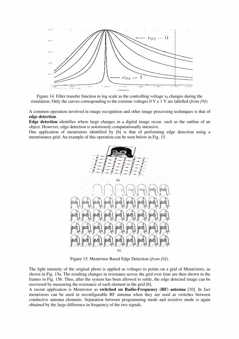
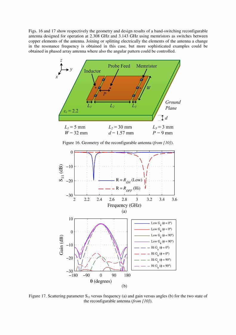
Figure 14. Filter transfer function in log scale as the controlling voltage vθ changes during the
simulation. Only the curves corresponding to the extreme voltages 0 V e 1 V are labelled (from [9]).
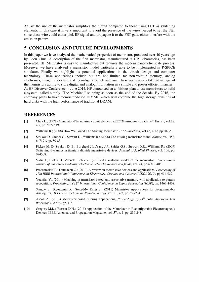
A common operation involved in image recognition and other image processing techniques is that of
edge detection.
Edge detection identifies where large changes in a digital image occur, such as the outline of an
object. However, edge detection is notoriously computationally intensive.
One application of memristors identified by [6] is that of performing edge detection using a
memristance grid. An example of this operation can be seen below in Fig. 15.
Figure 15. Memristor Based Edge Detection (from [6]).
The light intensity of the original photo is applied as voltages to points on a grid of Memristors, as
shown in Fig. 15a. The resulting changes in resistance across the grid over time are then shown in the
frames in Fig. 15b. Thus, after the system has been allowed to settle, the edge detected image can be
recovered by measuring the resistance of each element in the grid [6].
A recent application is Memristor as switched on Radio-Frequency (RF) antenna [10]. In fact
memristors can be used in reconfigurable RF antenna when they are used as switches between
conductive antenna elements. Separation between programming mode and resistive mode is again
obtained by the large difference in frequency of the two signals.
Figs. 16 and 17 show respectively the geometry and design results of a band-switching reconfigurable
antenna designed for operation at 2.308 GHz and 3.143 GHz using memristors as switches between
copper elements of the antenna. Joining or splitting electrically the elements of the antenna a change
in the resonance frequency is obtained in this case, but more sophisticated examples could be
obtained in phased array antenna where also the angular pattern could be controlled.
Figure 16. Geometry of the reconfigurable antenna (from [10]).
Figure 17. Scattering parameter S11 versus frequency (a) and gain versus angles (b) for the two state of
the reconfigurable antenna (from [10]).
At last the use of the memristor simplifies the circuit compared to those using FET as switching
elements. In this case it is very important to avoid the presence of the wires needed to set the FET
since these wire could either pick RF signal and propagate it to the FET gate, either interfere with the
emission pattern.
5. CONCLUSION AND FUTURE DEVELOPMENTS
In this paper we have analyzed the mathematical properties of memristor, predicted over 40 years ago
by Leon Chua. A description of the first memristor, manufactured at HP Laboratories, has been
presented. HP Memristor is easy to manufacture but requires the modern nanometre scale process.
Moreover we have analyzed a memristor model particularly able to be implemented in P-SPICE
simulator. Finally we highlight its potential applications in the circuit design and computer
technology. These applications include but are not limited to: non-volatile memory, analog
electronics, image processing and reconfigurable RF antenna. These applications take advantage of
the memristors ability to store digital and analog information in a simple and power efficient manner.
At HP Discover Conference in June 2014, HP announced an ambitious plan to use memristors to build
a system, called simply "The Machine," shipping as soon as the end of the decade. By 2016, the
company plans to have memristor-based DIMMs, which will combine the high storage densities of
hard disks with the high performance of traditional DRAM.
REFERENCES
[1] Chua L.; (1971) Memristor-The missing circuit element. IEEE Transactions on Circuit Theory, vol.18,
n.5, pp. 507- 519.
[2] Williams R.; (2008) How We Found The Missing Memristor. IEEE Spectrum, vol.45, n.12, pp.28-35.
[3] Strukov D., Snider G., Stewart D., Williams R.; (2008) The missing memristor found, Nature, vol. 453,
n. 7191, pp. 80-83.
[4] Pickett M. D, Strukov D. B., Borghetti J.L.,Yang J.J., Snider G.S., Stewart D.R., Williams R.; (2009)
Switching dynamics in titanium dioxide memristive devices, Journal of Applied Physics, vol. 106, pp.
074508.
[5] Valsa J., Biolek D., Zdenek Biolek Z.; (2011) An analogue model of the memristor, International
Journal of numerical modeling: electronic networks, devices and fields, vol. 24, pp.400 – 408.
[6] Prodromakis T.; Toumazou C.; (2010) A review on memristive devices and applications, Proceeding of
17th IEEE International Conference on Electronics, Circuits, and Systems (ICECS 2010), pp.934-937.
[7] Yuanfan Y.; (2014) Matching in memristor based auto-associative memory with application to pattern
recognition, Proceedings of 12th
International Conference on Signal Processing (ICSP), pp. 1463-1468.
[8] Sangho S.; Kyungmin K.; Sung-Mo Kang S.; (2011) Memristor Applications for Programmable
Analog ICs, IEEE Transactions on Nanotechnology, vol. 10, n.2, pp.266-274.
[9] Ascoli A.; (2013) Memristor-based filtering applications, Proceedings of 14th
Latin American Test
Workshop (LATW), pp. 1-6.
[10] Gregory M.D.; Werner D.H.; (2015) Application of the Memristor in Reconfigurable Electromagnetic
Devices, IEEE Antennas and Propagation Magazine, vol. 57, n. 1, pp. 239-248.
Authors
Roberto Marani received the Master of Science degree (cum laude) in Electronic
Engineering in 2008 from Polytechnic University of Bari, where he received his Ph.D.
degree in Electronic Engineering in 2012.
He worked in the Electronic Device Laboratory of Bari Polytechnic for the design,
realization and testing of nanometrical electronic systems, quantum devices and FET on
carbon nanotube. Moreover Dr. Marani worked in the field of design, modelling and
experimental characterization of devices and systems for biomedical applications.
In December 2008 he received a research grant by Polytechnic University of Bari for his
research activity. From February 2011 to October 2011 he went to Madrid, Spain, joining the Nanophotonics
Group at Universidad Autónoma de Madrid, under the supervision of Prof. García-Vidal.
Currently he is involved in the development of novel numerical models to study the physical effects that occur
in the interaction of electromagnetic waves with periodic nanostructures, both metal and dielectric. His research
activities also include biosensing and photovoltaic applications.
Dr. Marani is a member of the COST Action MP0702 - Towards Functional Sub-Wavelength Photonic
Structures, and is a member of the Consortium of University CNIT – Consorzio Nazionale Interuniversitario per
le Telecomunicazioni.
Dr. Marani has published over 100 scientific papers.
Gennaro Gelao received the Laurea degree in Physics from University of Bari, Italy, in
1993 and his Ph.D. degree in Physics from University of Bari in 1996, working at the
ALEPH experiment, CERN.
Dr. Gelao worked at the start-up of an electrical metrological laboratory at ENEA
(Rotondella, Italy)
Currently he cooperates with the Electronic Device Laboratory of Polytechnic University of
Bari for the design, realization and testing of nanometrical electronic systems, quantum
devices and CNTFETs. His research activity involves also the design and experimental
characterization of devices and systems for biomedical applications.
Dr. Gelao has published over 80 papers.
Anna Gina Perri received the Laurea degree cum laude in Electrical Engineering from
the University of Bari in 1977. In the same year she joined the Electrical and Electronic
Department, Polytechnic University of Bari, Italy, where she is Full Professor of Electronics
from 2002.
From 2003 she has been associated with the National Institute of Nuclear Phisics (INFN) of
Napoli (Italy), being a part of the TEGAF project: ”Teorie Esotiche per Guidare ed
Accelerare Fasci”, dealing with the optimal design of resonance-accelerating cavities having
very high potentials for cancer hadrontherapy.
In 2004 she was awarded the “Attestato di Merito” by ASSIPE (ASSociazione Italiana per la Progettazione
Elettronica), Milano, BIAS’04, for her studies on electronic systems for domiciliary teleassistance.
Her current research activities are in the area of numerical modelling and performance simulation techniques of
electronic devices for the design of GaAs Integrated Circuits and in the characterization and design of
optoelectronic devices on PBG (Phothonic BandGap).
Moreover she works in the design, realization and testing of nanometrical electronic systems, quantum devices,
FET on carbon nanotube and in the field of experimental characterization of electronic systems for biomedical
applications.
Prof. Perri is the Head of the Electron Devices Laboratory of the Polytechnic University of Bari.
She has been listed in the following volumes: Who’s Who in the World and Who’s Who in Engineering,
published by Marquis Publ. (U.S.A.).
She is author of over 250 journal articles, conference presentations, twelve books and currently serves as a
Referee of a number of international journals.
Prof. Perri is the holder of two italian patents and the Editor of two international books.
She is also responsible for research projects, sponsored by the Italian Government.

![Modeling of the Memristor in SPICE Introduction In 1971, professor Chua predicted the existence of the fourth circuit element – memristor [3]. The memristor](https://img.pdfslide.us/doc/110x75/56649e3b5503460f94b2d7a3/modeling-of-the-memristor-in-spice-introduction-in-1971-professor-chua-predicted.jpg)