Embed Size (px)
Citation preview
A REVIEW ON DESIGN OF PROGRAMMABLE VOLTAGE REGULATOR WITH INPUT OUTPUT
BUFFER USING VLSI TECHNOLOGY
Snehal N. Belorkar, Dr. A.S.Joshi (Department of Electronics and Telecommunication, Sipna College of Engineering and Technology
Sant Gadge Baba Amravati University, India)
Abstract— A Programmable voltage regulator with
Input– Output Differential Voltage with nm VLSI technology in
increasing the Density, provides for the new approaches towards
power management. Buffer is used in input and output of
programmable LDO circuit for matching input and output
impedance of circuit. Trans-Conductance Amplifier is used as the
Error Amplifier (EA), with a current splitting technique is
implemented to boost the gain. In the rail-to-rail output stage of
the Error Amplifier, Cancellation of power noise is formed,
minimizing the size of the Power MOS transistor. These helps the
proposed LDO Regulator to operate over a wide range of
operating conditions achieving maximum current efficiency,
output variation is less for a variable load transient, and effective
PSRR. The proposed LDO regulator is compact in nature which
leads to a efficient chip area. Low drop-out Voltage Regulator
has application in electronics devices, i.e. cellular phones, pagers,
laptops, etc
Keywords - low drop-out with input output buffer, 32nm, low
power consumption, programmability, low area.
I. INTRODUCTION The usage of the battery power devices in today’ s global village has become inescapable and necessary in almost every walk of life. The design gets reduced by reducing the battery cells. By minimizing quiescent current flow battery life increases. An increasing low voltage application requires LDOs, which include the growing family of battery products in industries. The main feature of voltage regulators provides a constant voltage supply rail under all loading conditions. Most battery-powered electronics equipment has feature that reduce power consumption. In the world of electronics low dropout and low supply characteristic of CMOS is used. Proposed LDO regulators enable battery to be used up to the certain voltage limits, and therefore the regulators are power management ICs for the electronics devices like mobile phones, digital cameras, and laptop PCs to have long battery life. Demand is increasing to design a stable Programmable LDO for a wide range of load conditions with
low drop-out voltage, low quiescent current and high PSR. But it is found to be difficult to improve all of them simultaneously. low power battery-operated circuits, demanding special emphasis is on compactness and portability. By using smaller transistor size enables faster transient response since slew-rate limit at the gate of the power transistor is relatively not serious [3]. The power management unit (PMU) concept is used to minimize supply voltage, faster dynamic response, higher stability, small area and less power consumption. Previously proposed architectures provide different techniques to isolate input and output along the high current signal path. It is seen that 32nm technology proves better performance. External control signals are used to change the feedback resistor divider ratio to achieve a programmable output voltage required for different applications used in electronics device. Basic structure of LDO regulator is composed of three main components-biasing circuits, an error amplifier, a power MOS device. The output stage design of the error amplifier has impact on the required size of power transistor. Power transistor improves load regulation especially when the supply voltage is low. Main focus is to design a proposed programmable low-dropout (LDO) voltage regulator that operate with a very small input output differential voltage with nm CMOS technology whose output voltage level is controlled externally by means of control signals. As future nm technology offers in achieving most of the performance specifications.
II. LITERATURE REVIEW 1)Ka Nang Leung, Yuan Yen Mai, Philip K. T. Mok, “ A Chip-Area Efficient Voltage Regulator for VLSI Systems” proposed a Chip-Area Efficient Voltage Regulator for VLSI system, the increase of the chip area due the proposed structure was very small when compare to the integrated power transistor. The load regulation of the proposed LDO is
International Journal of Scientific & Engineering Research, Volume 7, Issue 2, February-2016 ISSN 2229-5518 581
IJSER © 2016 http://www.ijser.org
IJSER
better, which corresponds to the reduction of the steady-state error of Vout by 0.55% 2)Mohamed El-Nozahiet.all used the concept of High PSR Low Drop-Out Regulator with Feed-Forward Ripple Cancellation Technique; the proposed topology provides a robust design when the process, temperature and bonding inductance variations were considered.LDO topology preserves traditional loop dynamics structure, while providing high PSR over a wide frequency range. In addition, it enables the design for high supply currents and low quiescent current consumption. 3)Chung-Hsun Huang, Ying-Ting Ma, Wei-Chen Liao “ Design of a Low-Voltage Low-Dropout Regulator” used the concept of Design of a Low-Voltage Low-Dropout Regulator in that paper presented an LDO regulator using a simple OTA-type EA plus an adaptive transient accelerator, which achieved operation below 1 V, fast transient response, low IQ,and high PSR under a wide range of operating conditions. The proposed LDO regulator was designed and fabricates dusing a 90-nm CMOS process to convert an input of 1 V to an output of 0.85– 0.5 V. 4) Jayanthi Vanama and G. L. Sampoorna,” Design of a programmable low power low drop-out regulator” ,they designed a low power low drop-out regulator that was capable of delivering four different output voltages, based on the control signals it receives. The design yields a 30 dB gain, but again of upto 50 dB may be achieved by further increase in transconductance of the differential pair. The design was disadvantaged from an input offset point of view, as the input offset error is up to 10 mV. Also, a folded cascade topology with resistive biasing can generate greater gain, reducing the number of stages and making phase margin of the system easier to accomplish at lower values of external capacitance.
III SPECIFICATIONS OF LDO
1. REGULATION Low-dropout (LDO) regulators work same as linear voltage regulators. The main difference between LDO and non-LDO regulators is their schematic. In non-LDO an emitter follower topology is used and In low-dropout regulators used open collector or open drain topology. This enables transistor saturation, which allows the voltage drop from the unregulated voltage to the regulated voltage. For high voltages under very low In-Out difference there will be power loss in the control circuit of device. Power FETs may be preferable to reduce power consumption, but this gives problems when it is used for low input voltage, as FETs usually require 5 to 10V to close completely. The cost of
Power FETs may also increase. The expected load & line regulation will be zero. 2. QUIESCENT CURRENT Linear regulator has characteristic that is the quiescent current, also known as ground current or supply current.LDO used quiescent current in order to control its internal circuitry for proper Operation. Quiescent current contribute series pass element, topologies, and ambient temperature..In idle state in order to keep internal circuitry ready when load is enabled LDO draws small amounts of quiescent current In order to minimize power loss while the LDO is idle, quiescent current should be as low as possible. If power consumption is less then portable application achieve long battery life. For high efficiency, the quiescent current must be minimized in electronics device. 3. POWER SUPPLY REJECTION Noise suppression responsible to provide clean and accurate output voltage with a low voltage level (≤1 V), High PSR can be achieved by an n-type power MOS transistor or a cascaded power MOS transistor. It is difficult to achieve a high loop gain with a low supply voltage. The power noise cancellation mechanism when used in circuit increases the design complexity and consumes extra IQ. Every step of design follow MICROWIND 3.1 software.
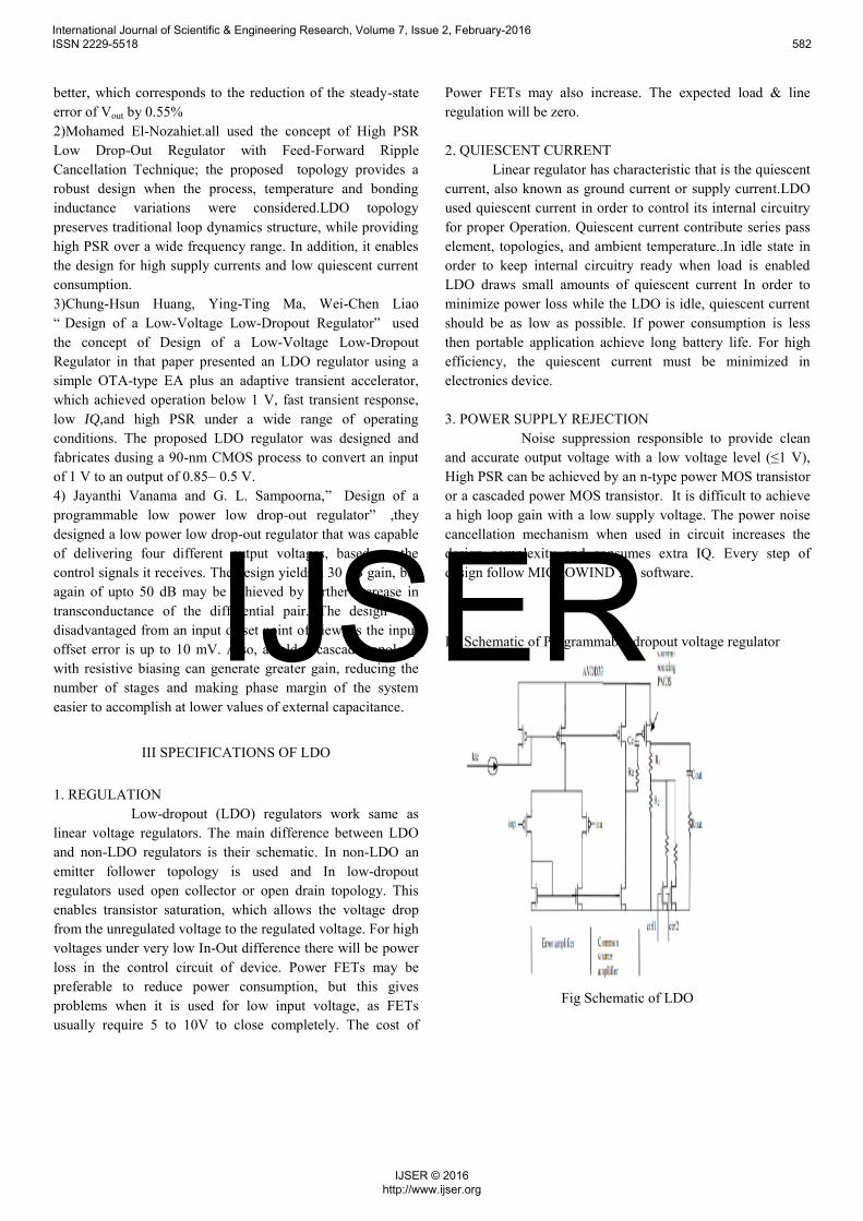
IV.Schematic of Programmable dropout voltage regulator
Fig Schematic of LDO
International Journal of Scientific & Engineering Research, Volume 7, Issue 2, February-2016 ISSN 2229-5518 582
IJSER © 2016 http://www.ijser.org
IJSER
V. Proposed Programmable voltage regulator using buffer A voltage reference is used with the op-amp to generate a regulated voltage. It provides an output voltage which is constant and it will be compared with the output voltage from the feedback network of circuit. If reference voltage is stable with temperature. Error amplifier produces in the circuit an error signal whenever the feedback output differs from the reference voltage. To drive any load; Pass Element provides the output current. PMOS pass transistor is used as pass element. This device must be very wide so that it can source large load currents with gate-source voltage. The length remains at the minimum value to keep the threshold voltage low. At the drain of PMOS, output voltage of the LDO and resistors R1 and R2 form a voltage divider in the circuitry. It is used to feed a fraction of the output voltage back to the input. R1 and R2 are made larger so that between them very little current flow, so that minimize the power consumption of the feedback path. Good line and load regulations provided by high loop gain. In proposed work architecture, a current-sourcing PMOS in the output stage is added. The PMOS be pulled down ground so as to be biased into saturation region is required. Because of this, the existing topology is modified with new architecture and a Common- Source Stage is added with the amplifying device. This large amplifying device is used so that it used as a strong pull down device. At the op-amp output, the Common-Source stage is responsible to enhance signal swing and boost the gain. The Common-Source stage also useful to pull the gate of the large PMOS. Gate of PMOS low so that its gate-to-source voltage increases. If the feedback voltage is smaller than the reference voltage, the gate of the PMOS device is pulled down to lower, so that more current is allowed to pass and increases the output voltage. And in second condition, if the feedback voltage is greater than the reference voltage, the gate of the PMOS device is pulled to higher, so that less current is passed and decreases the output voltage. Programmability is added to the LDO.Two control signals, ctrl1and ctrl2 are used which are applied at the gate inputs of two NMOS devices. The binary input controls the output voltage by biasing the transistor in saturation condition and brings résistance. The proposed architecture of programmable LDO consists of the following stages: I]Error Amplifier A high gain operational amplifier is used as the error amplifiers [4], with a stable voltage reference fed to one of its inputs while other to the ground. The differential pair of the operational amplifier is used which consists of a current
mirror circuit NMOS and a PMOS tail current source, along with the gate-drain connected load. A current mirror NMOS load is responsible to provide high output impedance. And it is also responsible for high gain. All nodes are low impedance nodes with the exception of the differential pair[8] in the operational amplifier which is known as open transconductance.The design of the output stage of the error amplifier has required size of the power transistor for the improvement of load regulation, especially when the supply voltage of the VLSI systems is low[3].
ii]Common-Source Amplifier In general, a source follower is used as the buffer stage in LDO’ s. The implementation of source follower is a simple of the buffer which uses natural NMOS transistor and it has limited gain. Hence a common-source amplifier is used. The gain of common source amplifier given by-
Av=gm (Ro1|| Ro2) Here, gm is the transconductance of the amplifying device; Ro1 and Ro2 are the output resistances of the load. When the amplifying device (NMOS) is made large enough, then we can improve gain at the second stage. NMOS also acts as a strong pull down device. Operational amplifiers with rail-to-rail output stage achieve the maximum output signal swing in systems with low single-supply voltages. Output signal is generated up to the supply rails. iii]Current-Sourcing PMOS In our design, a PMOS with high voltage threshold has been used. If a lower voltage threshold PMOS is used, then we can get advantage of lesser area but low-voltage threshold FETs are known to contribute to leakage currents, increasing power dissipation in the device. Therefore current-sourcing PMOS is used which is responsible for quick charging and discharging of the output node, capable of increasing slew rate to obtain faster settling times. iv]Compensation method The load is driven by an external capacitor, which is made large enough so that it can quickly charge the load during fast transients. However, the size of the capacitor is limited by the following constraints: the charging capability, the slew rate and the phase margin. Unlike most architecture where the dominant pole lies at the first node, here the dominant pole occurs at the output node as a result of which the external capacitor must be used as the compensation capacitor. Hence there is a lower limit on the size of the capacitor. However, for effective charging of the output node a large capacitor is necessary, but not too large that the output
International Journal of Scientific & Engineering Research, Volume 7, Issue 2, February-2016 ISSN 2229-5518 583
IJSER © 2016 http://www.ijser.org
IJSER
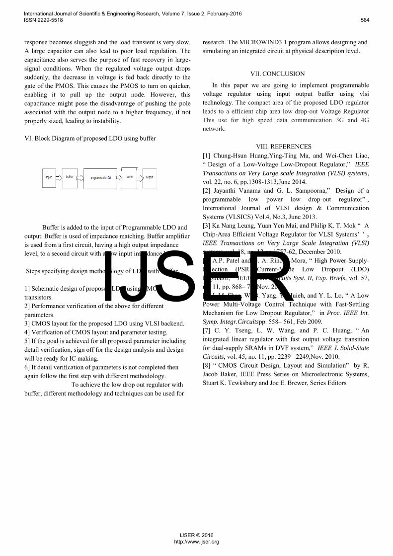
response becomes sluggish and the load transient is very slow. A large capacitor can also lead to poor load regulation. The capacitance also serves the purpose of fast recovery in large-signal conditions. When the regulated voltage output drops suddenly, the decrease in voltage is fed back directly to the gate of the PMOS. This causes the PMOS to turn on quicker, enabling it to pull up the output node. However, this capacitance might pose the disadvantage of pushing the pole associated with the output node to a higher frequency, if not properly sized, leading to instability. VI. Block Diagram of proposed LDO using buffer
Buffer is added to the input of Programmable LDO and output. Buffer is used of impedance matching. Buffer amplifier is used from a first circuit, having a high output impedance level, to a second circuit with a low input impedance level.
Steps specifying design methodology of LDO with Buffer 1] Schematic design of proposed LDO using CMOS transistors. 2] Performance verification of the above for different parameters. 3] CMOS layout for the proposed LDO using VLSI backend. 4] Verification of CMOS layout and parameter testing. 5] If the goal is achieved for all proposed parameter including detail verification, sign off for the design analysis and design will be ready for IC making. 6] If detail verification of parameters is not completed then again follow the first step with different methodology. To achieve the low drop out regulator with buffer, different methodology and techniques can be used for
research. The MICROWIND3.1 program allows designing and simulating an integrated circuit at physical description level.
VII. CONCLUSION
In this paper we are going to implement programmable voltage regulator using input output buffer using vlsi technology. The compact area of the proposed LDO regulator leads to a efficient chip area low drop-out Voltage Regulator This use for high speed data communication 3G and 4G network.
VIII. REFERENCES
[1] Chung-Hsun Huang,Ying-Ting Ma, and Wei-Chen Liao, “ Design of a Low-Voltage Low-Dropout Regulator,” IEEE
Transactions on Very Large scale Integration (VLSI) systems, vol. 22, no. 6, pp.1308-1313,June 2014. [2] Jayanthi Vanama and G. L. Sampoorna,” Design of a programmable low power low drop-out regulator” , International Journal of VLSI design & Communication Systems (VLSICS) Vol.4, No.3, June 2013. [3] Ka Nang Leung, Yuan Yen Mai, and Philip K. T. Mok “ A Chip-Area Efficient Voltage Regulator for VLSI Systems’ ’ ,
IEEE Transactions on Very Large Scale Integration (VLSI)
systems, vol. 18, no. 12,pp.1757-62, December 2010. [4] A.P. Patel and G. A. Rincon-Mora, “ High Power-Supply-Rejection (PSR Current-Mode Low Dropout (LDO) Regulator,” IEEE Trans.Circuits Syst. II, Exp. Briefs, vol. 57, no. 11, pp. 868– 73, Nov. 2010. [5] J. M. Shen, W. B. Yang. Y. Huieh, and Y. L. Lo, “ A Low Power Multi-Voltage Control Technique with Fast-Settling Mechanism for Low Dropout Regulator,” in Proc. IEEE Int.
Symp. Integr.Circuitspp. 558– 561, Feb 2009. [7] C. Y. Tseng, L. W. Wang, and P. C. Huang, “ An integrated linear regulator with fast output voltage transition for dual-supply SRAMs in DVF system,” IEEE J. Solid-State
Circuits, vol. 45, no. 11, pp. 2239– 2249,Nov. 2010. [8] “ CMOS Circuit Design, Layout and Simulation” by R. Jacob Baker, IEEE Press Series on Microelectronic Systems, Stuart K. Tewksbury and Joe E. Brewer, Series Editors
International Journal of Scientific & Engineering Research, Volume 7, Issue 2, February-2016 ISSN 2229-5518 584
IJSER © 2016 http://www.ijser.org
IJSER