Embed Size (px)
Citation preview

DATA SHEETwww.onsemi.com
© Semiconductor Components Industries, LLC, 2006
September, 2021 − Rev. 81 Publication Order Number:
FAN53526/D
Digitally ProgrammableTinyBuck� Regulator, 3.0 A, 2.4 MHz
FAN53526
DescriptionsThe FAN53526 is a step−down switching voltage regulator that
delivers a digitally programmable output from an input voltage supplyof 2.5 V to 5.5 V. The output voltage is programmed through an I2Cinterface capable of operating up to 3.4 MHz.
Using a proprietary architecture with synchronous rectification, theFAN53526 is capable of delivering 3.0 A continuous at over 80%efficiency, maintaining that efficiency at load currents as low as10 mA. The regulator operates at a nominal fixed frequency of2.4 MHz, which reduces the value of the external components.Additional output capacitance can be added to improve regulationduring load transients without affecting stability.
At moderate and light loads, Pulse Frequency Modulation (PFM) isused to operate in Power−Save Mode with a typical quiescent currentof 50 �A at room temperature. Even with such a low quiescent current,the part exhibits excellent transient response during large load swings.At higher loads, the system automatically switches to fixed−frequencycontrol, operating at 2.4 MHz. In Shutdown Mode, the supply currentdrops below 1 �A, reducing power consumption. PFM Mode can bedisabled if fixed frequency is desired. The FAN53526 is available in a15−bump, 1.310 mm x 2.015 mm, 0.4 mm ball pitch WLCSP.
Features• Fixed−Frequency Operation: 2.4 MHz
• Best−in−Class Load Transient
• Continuous Output Current Capability: 3.0 A
• 2.5 V to 5.5 V Input Voltage Range
• Digitally Programmable Output Voltage:♦ 0.600 V to 1.39375 V in 6.25 mV Steps
• Programmable Slew Rate for Voltage Transitions
• I2C−Compatible Interface Up to 3.4 Mbps
• PFM Mode for High Efficiency in Light-Load
• Quiescent Current in PFM Mode: 50 �A (Typical)
• Input Under−Voltage Lockout (UVLO)
• Thermal Shutdown and Overload Protection
• 15−Bump Wafer−Level Chip Scale Package (WLCSP)
Applications• Application, Graphic, and DSP Processors
♦ ARM�, Tegra�, OMAP�, NovaThor,ARMADA�, Krait�, etc.
• Hard Disk Drives, LPDDR3, LPDDR4
• Tablets, Netbooks, Ultra−Mobile PCs
• Smart Phones
• Gaming Devices
See detailed ordering and shipping information on page 2 ofthis data sheet.
ORDERING INFORMATION
WLCSP−15CASE 567QS
PGND AGND
VSEL SDAEN
SCL VOUTAGND
PGNDSWVIN
C1
B1
A1 A2
C3
B3
A3
C2
D1 D3D2
B2
E1 E3E2
PIN CONFIGURATION
MARKING DIAGRAM
1, 2 = Two Alphanumeric Characters for Device Mark
KK = Two Alphanumeric Characters for Lot Rune Code Mark
. = Pin 1 IndicatorX = Alphabetical Year CodeY = 2−weeks Date CodeZ = Assembly Plant Code
1Pin−1Mark
2 K K
X Y Z

FAN53526
www.onsemi.com2
FAN 53526 SW
COUT
L1
PVIN
PGND
CIN
VOUT
AGND
LOADVSEL
SCL
SDA
EN CIN_LOAD
CBY
Figure 1. Typical Application
Table 1. ORDERING INFORMATION
Part Number
Power−UpDefault (V)
DVS Range / Step Size
I2C SlaveAddress
TemperatureRange Package
PackingMethod
DeviceMarkingVSEL0 VSEL1
FAN53526UC84X 1.125 1.125
0.600 V to1.39375 V /
6.25 mV
C0
−40 to 85�C WLCSP Tape & Reel
F7
FAN53526UC89X 1.15625 1.15625 CL
FAN53526UC100X 1.225 1.225 F9
FAN53526UC106X 1.2625 1.2625 C7
FAN53526UC128X 1.20 1.20 F3
FAN53526UC00X 0.60 0.60 GA
FAN53526UC64X 1.00 1.00 GG
FAN53526UC88X 1.15 1.15 LM
FAN53526UC288X 1.15 1.15
C2
LN
FAN53526UC168X 1.125 1.125 FR
FAN53526UC224X 0.75 0.75 LL
RECOMMENDED EXTERNAL COMPONENTS
Table 2. RECOMMENDED EXTERNAL COMPONENTS FOR 3.0 A MAXIMUM LOAD CURRENT
Component Description Vendor Parameter Typ. Unit
L1 330 nH, 2016 Case SizeSee Table 3
L1 Alternative (Note 1) 470 nH 2016 Case Size
COUT1, COUT2 47 �F, 6.3 V, X5R, 0603 GRM188R60J476ME15 (Murata) C 47
�FCOUT1, COUT2 Alternative
(Note 1) 22 �F, 10 V, X5R, 0603 CL10A226MP8NUNB (SAMSUNG) C 22
CIN 1 Piece; 4.7 �F, 10 V, X5R, 0603 C1608X5R1A475K (TDK) C 4.7
CBY 1 Piece; 100 nF, 6.3V, X5R, 0201 GRM033R60J104KE19D (Murata) C 100 nF
1. COUT Alternative and L1 Alternative can be used if not following reference design. CBY is recommended to reduce any high frequencycomponent on VIN bus. CBY is optional and used to filter any high frequency component on VIN bus.

FAN53526
www.onsemi.com3
Table 3. RECOMMENDED INDUCTORS
Manufacturer Part # L (nH)DCR
(m� Typ.)ISAT
(Note 2) L W H
Toko DFE201612E−R33N 330 15 7.0 2.0 1.6 1.2
Toko DFE201612E−R47N 470 21 6.1 2.0 1.6 1.2
Cyntek PIFE20161B−R47MS−39 470 30 3.1 2.0 1.6 1.2
SEMCO CIGT201610UMR47MNE 470 30 4.0 2.0 1.6 0.9
SEMCO CIGT201610UMR47MNE 470 33 3.0 2.0 1.2 0.9
2. ISAT where the dc current drops the inductance by 30%.
PIN CONFIGURATION
PGND AGND
VSEL SDAEN
SCL VOUTAGND
PGNDSWVIN
C1
B1
A1 A2
C3
B3
A3
C2
D1 D3D2
B2
E1 E3E2
Figure 2. Pin Configuration
C1
B1
A1
C3
B3
A3 A2
C2
D1D3 D2
B2
E1E3 E2
Top View Bottom View
Table 4. PIN DEFINITIONS
Pin # Name Description
D1 VSEL
Voltage Select. When this pin is LOW, VOUT is set by the VSEL0 register. When this pin is HIGH,VOUT is set by the VSEL1 register. Polarity of pin in conjunction with the MODE bits in the Controlregister 02h, will select Forced PWM or Auto PFM/PWM mode of operation. VSEL0=Auto PFM,and VSEL1=FPWM. The VSEL pin has an internal pull−down resistor (250k�), which is only acti-vated with a logic low.
D2 ENEnable. The device is in Shutdown Mode when this pin is LOW. Device keeps register contentwhen EN pin is LOW. The EN Pin has an internal pull−down resistor (250k�), which is only activat-ed with a logic low.
E2 SCL I2C Serial Clock. If pin is unused, tie to AGND.
D3 SDA I2C Serial Data. If pin is unused, tie to AGND.
E3 VOUT VOUT. Sense pin for VOUT. Connect to COUT.
A3, B3, C2 PGNDPower Ground. The low−side MOSFET is referenced to this pin. CIN and COUT should be returnedwith a minimal path to these pins.
C3, E1 AGNDAnalog Ground. All signals are referenced to this pin. Avoid routing high dV/dt AC currents throughthis pin.
A1, B1, C1 VIN Power Input Voltage. Connect to the input power source. Connect to CIN with minimal path.
A2, B2 SW Switching Node. Connect to the inductor.

FAN53526
www.onsemi.com4
ABSOLUTE MAXIMUM RATINGSStresses exceeding the absolute maximum ratings may
damage the device. The device may not function or beoperable above the recommended operating conditions andstressing the parts to these levels is not recommended. In
addition, extended exposure to stresses above therecommended operating conditions may affect devicereliability. The absolute maximum ratings are stress ratingsonly.
Table 5. ABSOLUTE MAXIMUM RATINGS
Symbol Parameter Parameter Min Max Unit
VIN Voltage on SW, VIN Pins IC Not Switching −0.3 7.0 V
IC Switching −0.3 6.5
Voltage on EN Pin −0.3 VIN(Note 3)
Voltage on All Other Pins IC Not Switching −0.3 VIN(Note 3)
VOUT Voltage on VOUT Pin −0.3 6.5 V
VINOV_SLEW Maximum Slew Rate of VIN > 6.5V, PWM Switching 100 V/ms
ESD Human Body Model, ANSI/ESDA/JEDEC JS−001−2012 2000 V
Charged Device Model per JESD22−C101 1000
TJ Junction Temperature −40 +150 °C
TSTG Storage Temperature −65 +150 °C
TL Lead Soldering Temperature, 10 Seconds +260 °C
3. Lesser of 7V or VIN + 0.3 V.
RECOMMENDED OPERATING CONDITIONSThe Recommended Operating Conditions table defines
the conditions for actual device operation. Recommendedoperating conditions are specified to ensure optimal
performance to the datasheet specifications. onsemi doesnot recommend exceeding them or designing to AbsoluteMaximum Ratings.
Table 6. RECOMMENDED OPERATING CONDITIONS
Symbol Parameter Min. Typ. Max. Unit
VIN Supply Voltage Range 2.5 5.5 V
IOUT Output Current 0 3.0 A
TA Operating Ambient Temperature −40 +85 °C
TJ Operating Junction Temperature −40 +125 °C
Table 7. THERMAL PROPERTIES
Symbol Parameter Min. Typ. Max. Unit
θJAJunction−to−Ambient Thermal Resistance
(Note 4) 42 °C/W
4. Junction−to−ambient thermal resistance is a function of application and board layout. This data is simulated with four−layer 2s2p boards withvias in accordance to JESD51− JEDEC standard. Special attention must be paid not to exceed the junction temperature

FAN53526
www.onsemi.com5
ELECTRICAL CHARACTERISTICS
Table 8. ELECTRICAL CHARACTERISTICSMinimum and maximum values are at VIN=3.6 V, TA=-40°C to +85°C, unless otherwise noted. Typical values are at TA=25°C, VIN=3.6 V,
and EN=HIGH. VOUT = 1.15625 V.
Symbol Parameter Condition Min. Typ. Max. Unit
Power Supplies
IQ Quiescent CurrentILOAD=0 50 �A
ILOAD=0, MODE Bit=1 (Forced PWM) 15 mA
I SD
H/W Shutdown Supply Current EN=GND 0.1 3.0 �A
S/W Shutdown Supply CurrentEN=VIN, BUCK_ENx=0,2.5 V ≤ VIN ≤ 5.5 V 2 12 �A
VUVLO Under−Voltage Lockout Threshold VIN Rising 2.32 2.45 V
VUVHYST Under−Voltage Lockout Hysteresis 350 mV
EN, VSEL, SDA, SCL
VIH high−Level Input Voltage 2.5 V ≤ VIN ≤ 5.5 V 1.1 V
VIL low−Level Input Voltage 2.5 V ≤ VIN ≤ 5.5 V 0.4 V
IIN Input Bias Current Input Tied to GND or VIN 0.01 1.00 �A
VOUT Regulation
VREG VOUT DC Accuracy
2.5 V ≤ VIN ≤ 5.5 V, VOUT from Mini-mum to Maximum, IOUT(DC)=0 to3.0 A, Auto PFM/PWM
−2.5 2.5
%2.5 V ≤ VIN ≤ 5.5 V, VOUT from Mini-mum to Maximum, IOUT(DC)=0 to3.0 A, Forced PWM
−1.5 1.5
VIN=3.8 V, VOUT=0.6 V,IOUT(DC)=500 mA, Auto PFM/PWM
−2.3 −0.5
−14 −3 mV
�VOUT
�ILOAD
Load Regulation IOUT(DC)=1 to 3 A −0.01 %/A
�VOUT
�VIN
Line Regulation 2.5 V ≤ VIN ≤ 5.5 V, IOUT(DC)=1.5 A 0.01 %/A
VTRSP Transient Response
ILOAD Step 0.01 A ⇔ 1.5 A,tr=tf=200 ns, VOUT=1.15625 V ±50
mVILOAD Step 0 A ⇔ 500 mA,tr=tf=100 ns, VIN=3.8 V, VOUT=0.6 V ±16
Power Switch / Protection
ILIMPK P−MOS Peak Current Limit 4.00 4.75 5.50 A
TLIMIT Thermal Shutdown 150 °C
THYST Thermal Shutdown Hysteresis 17 °C
VSDWN Input OVP ShutdownRising Threshold 6.15
VFalling Threshold 5.50 5.73
Frequency Control
fSW Oscillator Frequency 2.05 2.40 2.75 MHz
DAC
Resolution 7 Bits
Differential Nonlinearity(5) 0.5 LSB
FAN53526
www.onsemi.com6
Table 8. ELECTRICAL CHARACTERISTICSMinimum and maximum values are at VIN=3.6 V, TA=-40°C to +85°C, unless otherwise noted. Typical values are at TA=25°C, VIN=3.6 V,
and EN=HIGH. VOUT = 1.15625 V.
Symbol UnitMax.Typ.Min.ConditionParameter
Soft−Start
tSSRegulator Enable to RegulatedVOUT
RLOAD > 5�, VOUT=1.15625V, FromEN Rising Edge to 95% VOUT
150 �s
5. Monotonicity assured by design.
Table 9. I2C TIMING SPECIFICATIONSMinimum and maximum values are at VIN=3.6 V, TA=-40°C to +85°C, unless otherwise noted. Typical values are at TA=25°C, VIN=3.6 V,
and EN=HIGH. VOUT = 1.15625 V.
Symbol Parameter Condition Min. Typ. Max. Unit
Power Supplies
fSCL SCL Clock Frequency
Standard Mode 100
kHz
Fast Mode 400
Fast Mode Plus 1000
High−Speed Mode, CB ≤ 100 pF 3400
High−Speed Mode, CB ≤ 400 pF 1700
tBUFBus−Free Time between STOP andSTART Conditions
Standard Mode 4.7
�sFast Mode 1.3
Fast Mode Plus 0.5
tHD;STASTART or REPEATED START Hold Time
Standard Mode 4 �s
Fast Mode 600
nsFast Mode Plus 260
High−Speed Mode 160
tLOW SCL LOW Period
Standard Mode 4.7
�sFast Mode 1.3
Fast Mode Plus 0.5
High−Speed Mode, CB ≤ 100 pF 160ns
High−Speed Mode, CB ≤ 400 pF 320
tHIGH SCL HIGH Period
Standard Mode 4 �s
Fast Mode 600
nsFast Mode Plus 260
High−Speed Mode, CB ≤ 100 pF 60
High−Speed Mode, CB ≤ 400 pF 120
tSU;STA Repeated START Setup Time
Standard Mode 4.7 �s
Fast Mode 600
nsFast Mode Plus 260
High−Speed Mode 160

FAN53526
www.onsemi.com7
Table 9. I2C TIMING SPECIFICATIONSMinimum and maximum values are at VIN=3.6 V, TA=-40°C to +85°C, unless otherwise noted. Typical values are at TA=25°C, VIN=3.6 V,
and EN=HIGH. VOUT = 1.15625 V.
Symbol UnitMax.Typ.Min.ConditionParameter
Power Supplies
tSU;DAT Data Setup Time
Standard Mode 250
nsFast Mode 100
Fast Mode Plus 50
High−Speed Mode 10
tHD;DAT Data Hold Time
Standard Mode 0 3.45 �s
Fast Mode 0 900
nsFast Mode Plus 0 450
High−Speed Mode, CB ≤ 100 pF 0 70
High−Speed Mode, CB ≤ 400 pF 0 150
tRCL SCL Rise Time
Standard Mode 20+0.1CB 1000
ns
Fast Mode 20+0.1CB 300
Fast Mode Plus 20+0.1CB 120
High−Speed Mode, CB ≤ 100 pF 10 80
High−Speed Mode, CB ≤ 400 pF 20 160
tFCL SCL Fall Time
Standard Mode 20+0.1CB 300
ns
Fast Mode 20+0.1CB 300
Fast Mode Plus 20+0.1CB 120
High−Speed Mode, CB ≤ 100 pF 10 40
High−Speed Mode, CB ≤ 400 pF 20 80
tRCL1
Rise Time of SCL After a RE-PEATED START Condition and Af-ter ACK Bit
High−Speed Mode, CB ≤ 100 pF 10 80ns
High−Speed Mode, CB ≤ 400 pF 20 160
tRDA SDA Rise Time
Standard Mode 20+0.1CB 1000
ns
Fast Mode 20+0.1CB 300
Fast Mode Plus 20+0.1CB 120
High−Speed Mode, CB ≤ 100 pF 10 80
High−Speed Mode, CB ≤ 400 pF 20 160
tFDA SDA Fall Time
Standard Mode 20+0.1CB 300
ns
Fast Mode 20+0.1CB 300
Fast Mode Plus 20+0.1CB 120
High−Speed Mode, CB ≤ 100 pF 10 80
High−Speed Mode, CB ≤ 400 pF 20 160
tSU;STO Stop Condition Setup Time
Standard Mode 4 �s
Fast Mode 600
nsFast Mode Plus 120
High−Speed Mode 160
CB Capacitive Load for SDA and SCL 400 pF

FAN53526
www.onsemi.com8
Timing Diagrams
ÎÎÎÎÎÎÎÎÎÎÎÎÏÏÏÏ
START
ÌÌÌÌÌÌÌÌÌÌÌÌ
ÑÑÑÑÑÑÑÑÑÑÑÑÓÓÓ
ÓÓÓ
REPEATEDSTART
ÔÔÔÔÔÔÔÔÔÔÔÔ
SCL
SDA
tF
tHD;STA
tLOW
tR
tHD;DAT
tHIGH
TSU;DAT
tSU;STA
tHD;STO
tBUF
ÖÖÖÖ
START ÒÒÒÒ
STOP
tHD;STA
Figure 3. I2C Interface Timing for Fast Plus, Fast, and Slow Modes
ÕÕÕÕÕÕÕÕÕÕ
ŠŠŠŠŠŠŠŠ
REPEATEDSTARTÚÚ
ÚÚÚÚÚÚÚÚÚÚÚÚ
SCLH
SDAH
tFDA
tLOW
tRCL1
tHD;DAT
tHIGH
tSU;STO
ÛÛÛÛÛÛ
REPEATEDSTART
tRDA
tFCL
tSU;DAT
tRCL
ÜÜÜÜÜÜ
STOPÙÙÙÙ
= MCS Current Source Pull−up
= RP Resistor Pull−up
note A
Note A: First rising edge of SCLH after Repeated Start and after each ACK bit.
tHD;STA
tSU;STA
Figure 4. I2C Interface Timing for High−Speed Mode
FAN53526
www.onsemi.com9
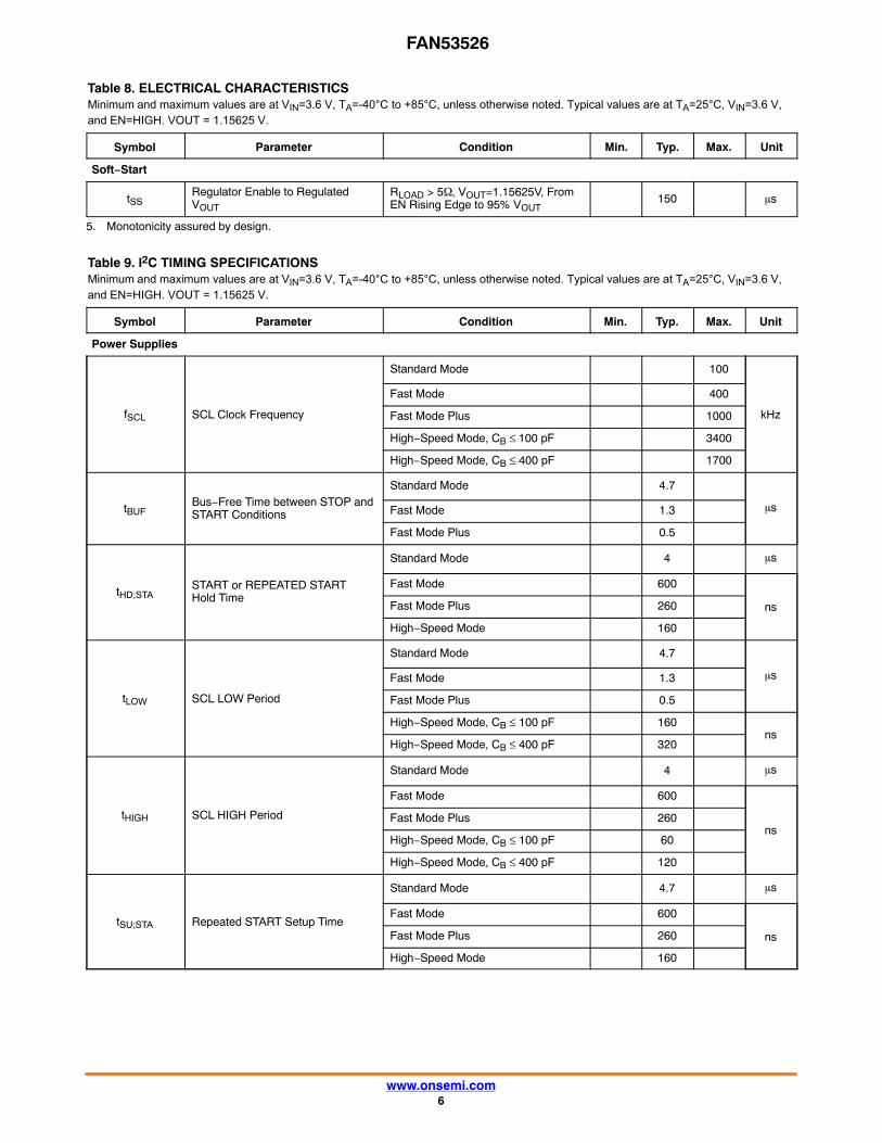
TYPICAL CHARACTERISTICS(Unless otherwise specified, Auto PFM/PWM Mode, VIN = 3.6 V, VOUT = 1.15625V, VSEL = EN = VIN, TA = 25°C; circuit and components
according to Figure 1 and Table 2. Efficiency test conditions; ILOAD: 1 mA to 3 A, L = 330 nH, DFE201612E−R33N (Toko). CIN = 4.7 �F,
0603, C1608X5R1A475K (TDK), COUT x 2 = 2X47 �F, 0603, GRM188R60J476ME (Murata).)
Figure 5. Efficiency vs. Load Current and InputVoltage, VOUT=1.15625V
Figure 6. Efficiency vs. Load Current andTemperature, VIN=3.6V, VOUT=1.15625V
Figure 7. Output Regulation vs. Load Current andInput Voltage, VOUT=1.15625V
Figure 8. PWM Entry / Exit Level vs. Input Voltage,VOUT=1.15625V
Figure 9. Output Ripple vs. Load Current, VIN=4.2Vand 3.6V, VOUT=1.15625V, Auto and Forced PWM
Figure 10. Frequency vs. Load Current, VIN=4.2Vand 3.6V, VOUT=1.15625V, Auto PWM
FAN53526
www.onsemi.com10
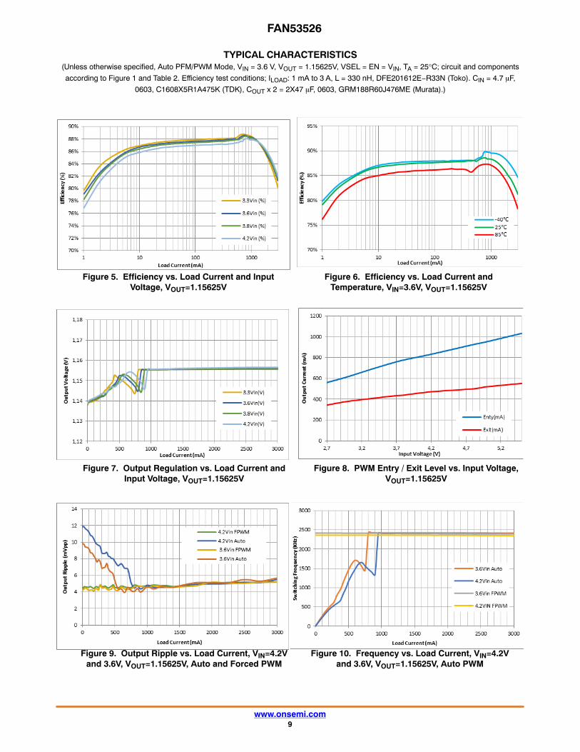
TYPICAL CHARACTERISTICS (continued)
(Unless otherwise specified, Auto PFM/PWM Mode, VIN = 3.6 V, VOUT = 1.15625V, VSEL = EN = VIN, TA = 25°C; circuit and components
according to Figure 1 and Table 2. Efficiency test conditions; ILOAD: 1 mA to 3 A, L = 330 nH, DFE201612E−R33N (Toko). CIN = 4.7 �F,
0603, C1608X5R1A475K (TDK), COUT x 2 = 2X47 �F, 0603, GRM188R60J476ME (Murata).)
Figure 11. Quiescent Current vs. Input Voltage andTemperature, Auto Mode, VOUT=1.15625V
Figure 12. Shutdown Current vs. Input Voltage andTemperature
VIN
VOUT
Figure 13. Line Transient, 3.6−4.2 VIN, 1.15625VOUT, 10 �s Edge at 1 A Load
IOUT
VOUT
Figure 14. Load Transient, 3.6 VIN, 1.15625 VOUT,0.01−1.5 A, 120 ns Edge
EN
VOUT
Figure 15. Startup, 5 � Load, VOUT = 1.15625 V,VIN = 3.6 V
IOUT
VOUT
Figure 16. Load Transient, 3.6 VIN, 1.15625 VOUT,1.5−3 A, 120 ns Edge

FAN53526
www.onsemi.com11
TYPICAL CHARACTERISTICS (continued)
(Unless otherwise specified, Auto PFM/PWM Mode, VIN = 3.6 V, VOUT = 1.15625V, VSEL = EN = VIN, TA = 25°C; circuit and components
according to Figure 1 and Table 2. Efficiency test conditions; ILOAD: 1 mA to 3 A, L = 330 nH, DFE201612E−R33N (Toko). CIN = 4.7 �F,
0603, C1608X5R1A475K (TDK), COUT x 2 = 2X47 �F, 0603, GRM188R60J476ME (Murata).)
IOUT (9500mA/div)
0mA
500mA
VOUT (10mV/div)0.6V offset
618mV
+ 16mV
− 16mV
582mV
Figure 17. Load Transient, 3.8 VIN, 0.6 VOUT, 0−500mA, 100 ns Edge, 47 �F COUT
Operating DescriptionThe FAN53526 is a step−down switching voltage
regulator that delivers a programmable output voltage froman input voltage supply of 2.5 V to 5.5 V. Using a proprietaryarchitecture with synchronous rectification, the FAN53526is capable of delivering 3.0 A at over 80% efficiency. Theregulator operates at a nominal frequency of 2.4 MHz at fullload, which reduces the value of the external components to330 nH or 470 nH for the output inductor and 44 μF for theoutput capacitor. High efficiency is maintained at light loadwith single−pulse PFM.
An I2C−compatible interface allows transfers up to3.4 Mbps. This communication interface can be used to:• Dynamically re−program the output voltage in 6.25 mV
increments;• Reprogram the mode to enable or disable PFM;
• Control voltage transition slew rate; or
• Enable / disable the regulator.
Control SchemeThe FAN53526 uses a proprietary non−linear,
fixed−frequency PWM modulator to deliver a fast loadtransient response, while maintaining a constant switchingfrequency over a wide range of operating conditions. Theregulator performance is independent of the outputcapacitor ESR, allowing for the use of ceramic outputcapacitors. Although this type of operation normally resultsin a switching frequency that varies with input voltage andload current, an internal frequency loop holds the switchingfrequency constant over a large range of input voltages andload currents.
For very light loads, the FAN53526 operates inDiscontinuous Current Mode (DCM) single−pulse PFM,which produces low output ripple compared with other PFMarchitectures. Transition between PWM and PFM isrelatively seamless, providing a smooth transition betweenDCM and CCM Modes.
PFM can be disabled by programming the MODE bits inthe CONTROL register in combination with the state of theVSEL pin. See table in the Control Register, 02h.
Enable and Soft−StartWhen the EN pin is LOW; the IC is shut down, all internal
circuits are off, and the part draws very little current. In thisstate, I2C can be written to or read from as long as inputvoltage is above the UVLO. The registers keep the contentwhen the EN pin is LOW. The registers are reset to defaultvalues during a Power On Reset (POR). When theOUTPUT_DISCHARGE bit in the Control register isenabled (logic HIGH) and the EN pin is LOW or theBUCK_ENx bit is LOW, an 11 W load is connected fromVOUT to GND to discharge the output capacitors.
Raising EN while the BUCK_ENx bit is HIGH activatesthe part and begins the soft−start cycle. During soft−start, themodulator’s internal reference is ramped slowly to minimizesurge currents on the input and prevent overshoot of theoutput voltage. Synchronous rectification is inhibited,allowing the IC to start into a pre−charged capacitive load.
If large values of output capacitance are used, theregulator may fail to start. The maximum COUT capacitancefor starting with a heavy constant−current load isapproximately:

FAN53526
www.onsemi.com12
COUTMAX � (ILMPK � ILOAD) �320�
VOUT
(eq. 1)
where COUTMAX is expressed in μF and ILOAD is theload current during soft−start, expressed in A.
If the regulator is at its current limit for 16 consecutivecurrent limit cycles, the regulator shuts down and enters
tri−state before reattempting soft−start 1700 �s later. Thislimits the duty cycle of full output current during soft−startto prevent excessive heating.
The IC allows for software enable of the regulator, whenEN is HIGH, through the BUCK_EN bits. BUCK_EN0 andBUCK_EN1 are both initialized HIGH. These options startafter a POR, regardless of the state of the VSEL pin.
Table 10. HARDWARE AND SOFTWARE ENABLE
Pins BITS
EN VSEL BUCK_EN0 BUCK_EN1 Output Mode
0 X X X OFF Shutdown
1 0 0 X OFF Shutdown
1 0 1 X ON Auto
1 1 X 0 OFF Shutdown
1 1 X 1 ON FPWM
VSEL Pin and I2C Programming Output VoltageThe output voltage is set by the NSELx control bits in
VSEL0 and VSEL1 registers. The output is given as:
VOUT � 0.600V � NSELx � 6.25mV (eq. 2)
For example, if NSEL =1010000 (80 decimal), then VOUT= 0.600 + 0.5 = 1.100 V.
Output voltage can also be controlled by toggling theVSEL pin LOW or HIGH. VSEL LOW corresponds toVSEL0 and VSEL HIGH corresponds to VSEL1. Upon
POR, VSEL0 and VSEL1 are reset to their default voltages,as shown in Table 8.
Transition Slew Rate LimitingWhen transitioning from a low to high voltage, the IC can
be programmed for one of eight possible slew rates using theSLEW bits in the Control register, as shown in the tablebelow.
Table 11. TRANSITION SLEW RATE
Decimal Bin Slew Rate
0 000 64.00 mV/�s
1 001 32.00 mV/�s
2 010 16.00 mV/�s
3 011 8.00 mV/�s
4 100 4.00 mV/�s
5 101 2.00 mV/�s
6 110 1.00 mV/�s
7 111 0.50 mV/�s
Transitions from high to low voltage rely on the outputload to discharge VOUT to the new set point. Once thehigh−to−low transition begins, the IC stops switching untilVOUT has reached the new set point.
Under−Voltage Lockout (UVLO)When EN is HIGH, the under−voltage lockout keeps the
part from operating until the input supply voltage risesHIGH enough to properly operate. This ensures properoperation of the regulator during startup or shutdown.
Input Over−Voltage Protection (OVP)When VIN exceeds VSDWN (~ 6.2 V), the IC stops
switching to protect the circuitry from internal spikes above6.5 V. An internal filter prevents the circuit from shuttingdown due to noise spikes.
Current LimitingA heavy load or short circuit on the output causes the
current in the inductor to increase until a maximum currentthreshold is reached in the high−side switch. Upon reaching
FAN53526
www.onsemi.com13
this point, the high−side switch turns off, preventing highcurrents from causing damage. 16 consecutive current limitcycles in current limit, cause the regulator to shut down andstay off for about 1700 �s before attempting a restart.
Thermal ShutdownWhen the die temperature increases, due to a high load
condition and/or high ambient temperature, the outputswitching is disabled until the die temperature fallssufficiently. The junction temperature at which the thermalshutdown activates is nominally 150°C with a 17°Chysteresis.
Monitor Register (Reg05)The Monitor register indicates of the regulation state of
the IC. If the IC is enabled and is regulating, its value is(1000 0001).
I2C InterfaceThe serial interface is compatible with Standard, Fast,
Fast Plus, and HS Mode I2C Bus� specifications. The SCLline is an input and its SDA line is a bi−directionalopen−drain output; it can only pull down the bus whenactive. The SDA line only pulls LOW during data reads andwhen signaling ACK. All data is shifted in MSB (bit 7) first.
I2C Slave AddressIn hex notation, the slave address assumes a 0 LS Bit. The
hex slave address is C0 for all options exceptFAN53526UC168X, which has a hex slave address of C2.
Table 12. I2C SLAVE ADDRESS
HexBits
7 6 5 4 3 2 1 0
C0 1 1 0 0 0 0 0
C2 1 1 0 0 0 0 1
Other slave addresses can be assigned. Contact an onsemirepresentative.
Bus TimingAs shown in Figure 18 data is normally transferred when
SCL is LOW. Data is clocked in on the rising edge of SCL.Typically, data transitions shortly at or after the falling edgeof SCL to allow sufficient time for the data to set up beforethe next SCL rising edge.
SCL tSU
tH
SDA
Data change allowed
Figure 18. Data Transfer TimingEach bus transaction begins and ends with SDA and SCL
HIGH. A transaction begins with a START condition, whichis defined as SDA transitioning from 1 to 0 with SCL HIGH,as shown in Figure 19.
SCL
tHD;STASDA
Slave AddressMS Bit
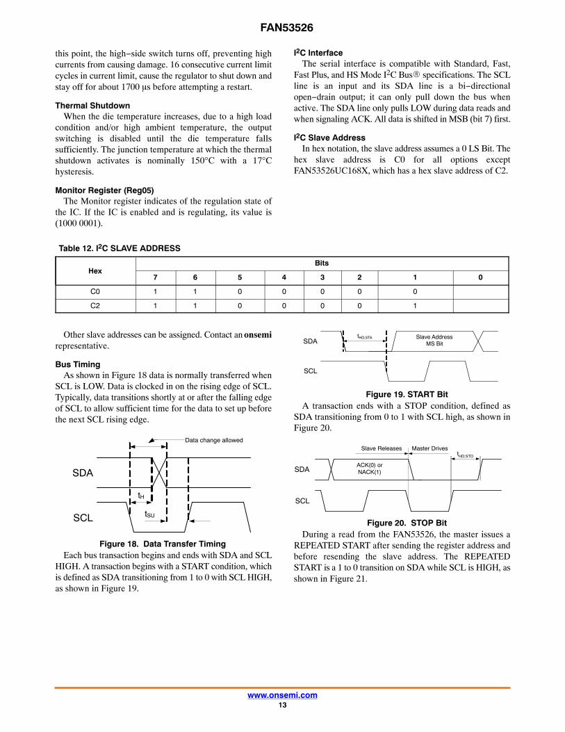
Figure 19. START BitA transaction ends with a STOP condition, defined as
SDA transitioning from 0 to 1 with SCL high, as shown inFigure 20.
SCL
SDA
Slave Releases Master Drives
ACK(0) orNACK(1)
tHD;STO
Figure 20. STOP BitDuring a read from the FAN53526, the master issues a
REPEATED START after sending the register address andbefore resending the slave address. The REPEATEDSTART is a 1 to 0 transition on SDA while SCL is HIGH, asshown in Figure 21.

FAN53526
www.onsemi.com14
SCL
SDAACK(0) orNACK(1)
Slave Releases
SLADDRMS Bit
tHD;STAtSU;STA
Figure 21. REPEATED START Timing
High−Speed (HS) ModeThe protocols for High−Speed (HS), Low−Speed (LS),
and Fast−Speed (FS) Modes are identical; except the busspeed for HS Mode is 3.4 MHz. HS Mode is entered whenthe bus master sends the HS master code 00001XXX aftera START condition (Figure 19). The master code is sent inFast or Fast−Plus Mode (less than 1 MHz clock); slaves donot ACK this transmission.
The master generates a REPEATED START condition(Figure 21) that causes all slaves on the bus to switch to HSMode. The master then sends I2C packets, as describedabove, using the HS Mode clock rate and timing.
The bus remains in HS Mode until a STOP bit (Figure 20)is sent by the master. While in HS Mode, packets areseparated by REPEATED START conditions (Figure 21).
Read and Write TransactionsThe following figures outline the sequences for data read
and write. Bus control is signified by the shading of thepacket, defined as:
• Master Drives Bus and
• Slave Drives Bus
All addresses and data are MSB first.
Table 13. I2C BIT DEFINITIONS FOR FIGURE 22 AND FIGURE 23
Symbol Definition
S START, see Figure 19
P STOP, see Figure 20
R REPEATED START, see Figure 21
A ACK. The slave drives SDA to 0 acknowledge the preceding packet.
A NACK. The slave sends a 1 to NACK the preceding packet.
S Slave Address A Reg Addr A A P0
7 bits 8 bits 8 bits
Data
0 0 0
Figure 22. Write Transaction
S Slave Address A Reg Addr A0
7 bits 8 bits
R Slave Address
7 bits
1 A Data A
8 bits0 0 0 1
P
Figure 23. Write Transaction Followed by a Read Transaction

FAN53526
www.onsemi.com15
REGISTER DESCRIPTION
Table 14. REGISTER MAP
Hex Address Name Function Binary Hex
00 VSEL0 Controls VOUT settings when VSEL pin = LOW 1XXXXXXX XX
01 VSEL1 Controls VOUT settings when VSEL pin = HIGH 1XXXXXXX XX
02 CONTROLDetermines whether VOUT output discharge is enabled and also the slew rateof positive transitions 10000010 82
03 ID1 Read−only register identifies vendor and chip type 10000001 81
04 ID2 Read−only register identifies die revision 00001000 08
05 MONITOR Indicates device status 00000000 00
Table 15. BIT DEFINITIONS
Bit Name Type Value Description
VSEL0 Register Address: 00
7 BUCK_EN0 R/W 1Software buck enable. When EN pin is LOW, the regulator isoff. When EN pin is HIGH, BUCK_EN bit takes precedent.
6:0 NSEL0 R/W XXX XXXX Sets VOUT value from 0.600 to 1.39375 V (see Eq.2).
VSEL1 Register Address: 01
7 BUCK_EN1 R/W 1Software buck enable. When EN pin is LOW, the regulator isoff. When EN pin is HIGH, BUCK_EN bit takes precedent.
6:0 NSEL1 R/W XXX XXXX Sets VOUT value from 0.600 to 1.39375 V (see Eq.2).
CONTROL Register Address: 02
7 OUTPUT_ DISCHARGE R/W
0 When the regulator is disabled, VOUT is not discharged.
1 When the regulator is disabled, VOUT discharges through aninternal pull−down.
6:4 SLEWR/W
000 –111Sets the slew rate for positive voltage transitions (see Transi-tion Slew Rate Limiting for details.)
3 Reserved 0 Always reads back 0.
2 RESETR/W 0 Setting to 1 resets all registers to default values. Always reads
back 0.
1:0 MODE R/W 10
In combination with the VSEL pin, these two bits set the opera-tion of the buck to be either in Auto−PFM/PWM Mode duringlight load or Forced PWM mode. See table below.Mode of Operation
VSEL Pin Binary Operation
Low X0 Auto PFM/PWMLow X1 Forced PWMHigh 0X Auto PFM/PWMHigh 1X Forced PWM
ID1 Register Address: 03
7:5 VENDOR R 100 Signifies onsemi as the IC vendor.
4 Reserved R 0 Always reads back 0.
3:0 DIE_ID R 0001 DIE ID − FAN53525/6.
ID2 Register Address: 04
7:4 Reserved R 0000 Always reads back 0000.
3:0 DIE_REV R 1000 FAN53526 Die Revision

FAN53526
www.onsemi.com16
Table 15. BIT DEFINITIONS
Bit DescriptionValueTypeName
MONITOR Register Address: 05
7 PGOOD R 0 1: Buck is enabled and soft−start is completed.
6 UVLO R 0 1: Signifies the VIN is less than the UVLO threshold.
5 OVP R 0 1: Signifies the VIN is greater than the OVP threshold.
4 POSR 0 1: Signifies a positive voltage transition is in progress and the
output voltage has not yet reached its new setpoint.
3 NEGR 0 1: Signifies a negative voltage transition is in progress and the
output voltage has not yet reached its new setpoint.
2 RESET−STATR 0 1: Indicates that a register reset was performed. This bit is
cleared after register 5 is read.
1 OT R 0 1: Signifies the VIN is less than the UVLO threshold.
0 BUCK_STATUS R 0 1: Signifies the VIN is greater than the OVP threshold.
APPLICATION INFORMATION
Selecting the InductorThe output inductor must meet both the required
inductance and the energy−handling capability of theapplication. The inductor value affects the average currentlimit, the output voltage ripple, and the efficiency.
The ripple current (ΔI) of the regulator is:
�I �VOUT
VIN
� �VIN�VOUT
L � fSW
�(eq. 3)
The maximum average load current, IMAX(LOAD), isrelated to the peak current limit, ILIM(PK), by the ripplecurrent such that:
IMAX(LOAD) � ILIM(PK)��I
2 (eq. 4)
The FAN53526 is optimized for operation withL=330 nH, but is stable with inductances up to 1.0 μH(nominal). The inductor should be rated to maintain at least
80% of its value at ILIM(PK). Failure to do so decreases theamount of DC current the IC can deliver.
Efficiency is affected by the inductor DCR and inductancevalue. Decreasing the inductor value for a given physicalsize typically decreases the DCR; but since ΔI increases, theRMS current increases, as do core and skin−effect losses:
IRMS � IOUT(DC)2 �
�I2
12 (eq. 5)
The increased RMS current produces higher lossesthrough the RDS(ON) of the IC MOSFETs and the inductorESR.
Increasing the inductor value produces lower RMScurrents, but degrades transient response. For a givenphysical inductor size, increased inductance usually resultsin an inductor with lower saturation current.
Table 16. EFFECTS OF INDUCTOR VALUE (FROM 330NH RECOMMENDED) ON REGULATORPERFORMANCE
IMAX(LOAD) �VOUT(Eq.(7)) Transient Response
Increase Decrease Degraded
Inductor Current RatingThe current-limit circuit can allow substantial peak
currents to flow through L1 under worst−case conditions. Ifit is possible for the load to draw such currents, the inductorshould be capable of sustaining the current or failing in a safemanner.
For space−constrained applications, a lower current ratingfor L1 can be used. The FAN53526 may still protect theseinductors in the event of a short circuit, but may not be ableto protect the inductor from failure if the load is able to drawhigher currents than the DC rating of the inductor. Refer toTable 2 for the recommended inductors.
Output Capacitor and VOUT RippleIf space is at a premium, 0603 capacitors may be used.Increasing COUT has negligible effect on loop stability
and can be increased to reduce output voltage ripple or toimprove transient response. Output voltage ripple, �VOUT,is calculated by:
�VOUT � �ILfSW � COUT � ESR2
2 � D � (1 � D)�
1
8 � fSW � COUT
� (eq. 6)
where COUT is the effective output capacitance.

FAN53526
www.onsemi.com17
The capacitance of COUT decreases at higher outputvoltages, which results in higher �VOUT. Equation 6 is onlyvalid for CCM operation, which occurs in PWM Mode.
The FAN53526 can be used with either 2 x 22 �F (0603)or 2 x 47 �F (0603) output capacitor configuration. If atighter ripple and transient specification is need from theFAN53526, then the 2 x 47 �F is recommended.
The lowest �VOUT is obtained when the IC is in PWMMode and, therefore, operating at 2.4 MHz. In PFM Mode,fSW is reduced, causing �VOUT to increase.
ESL EffectsThe Equivalent Series Inductance (ESL) of the output
capacitor network should be kept low to minimize thesquare−wave component of output ripple that results fromthe division ratio COUT ESL and the output inductor (LOUT).The square−wave component due to the ESL can beestimated as:
�VOUT(SQ) � VIN �ESL
COUT
L1 (eq. 7)
A good practice to minimize this ripple is to use multipleoutput capacitors to achieve the desired COUT value. Forexample, to obtain COUT=20 �F, a single 22 �F 0805 wouldproduce twice the square wave ripple as two x 10 �F 0805.
To minimize ESL, try to use capacitors with the lowestratio of length to width. 0805 s have lower ESL than 1206 s.If low output ripple is a chief concern, some vendorsproduce 0508 capacitors with ultra−low ESL. Placingadditional small−value capacitors near the load also reducesthe high−frequency ripple components.
Input CapacitorThe ceramic input capacitors should be placed as close as
possible between the VIN and PGND pins to minimize theparasitic inductance. If a long wire is used to bring power tothe IC, additional “bulk” capacitance (electrolytic ortantalum) should be placed between CIN and the powersource lead to reduce under−damped ringing that can occurbetween the inductance of the power source leads and CIN.
Thermal ConsiderationsHeat is removed from the IC through the solder bumps to
the PCB copper. The junction−to−ambient thermalresistance (θJA) is largely a function of the PCB layout (size,copper weight, and trace width) and the temperature risefrom junction to ambient (ΔT).
For the FAN53526, θJA is 42°C/W when mounted on itsfour−layer with vias evaluation board in still air with 2 oz.outer layer copper weight and 1 oz. inner layer.
For long−term reliable operation, the junctiontemperature (TJ) should be maintained below 125°C.
To calculate maximum operating temperature (<125°C)for a specific application:
1. Use efficiency graphs to determine efficiency forthe desired VIN, VOUT, and load conditions.
2. Calculate total power dissipation using:
PT � VOUT � ILOAD � �1� � 1� (eq. 8)
3. Estimate inductor copper losses using:
PL � ILOAD2 � DCRL (eq. 9)
4. Determine IC losses by removing inductor losses(step 3) from total dissipation:
PIC � PT � PL (eq. 10)
5. Determine device operating temperature:
�T � PIC � �JA TIC � TA � �T(eq. 11)
andNote that the RDS(ON) of the power MOSFETs increases
linearly with temperature at about 1.4%/°C. This causes theefficiency (η) to degrade with increasing die temperature.
Layout Recommendations1. The input capacitor (CIN) should be connected as
close as possible to the VIN and GND pins.Connect to VIN and GND using only top metal. Do not route through vias.
2. Place the inductor (L) as close as possible to theIC. Use short wide traces for the main currentpaths.
3. The output capacitor (COUT) should be as close aspossible to the IC. Connection to GND should beon top metal. Feedback signal connection toVOUT should be routed away from noisycomponents and traces (e.g. SW line). For remotesensing application, place one or all outputcapacitors near the load and if there are also outputcapacitors placed near the inductor, the maximumtrace resistance between the inductor and the loadshould not exceed 30 m�.

FAN53526
www.onsemi.com18
Figure 24. Guidance for Layer 1
Figure 25. Layer 2 Figure 26. Layer 3

FAN53526
www.onsemi.com19
Figure 27. Layer 4
EN
SDA
SCL
VSEL
FAN53526
VIN
VOUT
SW
PGND
AGND
CIN
GND
VDD
CoreProcessor
(System Load)
1. Feedback trace connects to “+” side of the output capacitor.
2. For remote sensing, place one or all outputcapacitors near the load.
3. If there are also output capacitors placed near the inductor, the maximum trace resistance betweenthe inductor and the load should not exceed 30 m�.
L1
CBY
COUT COUT_LOAD
Figure 28. Remote Sensing Schematic
Table 17. PRODUCT SPECIFIC DIMENSIONS
D E X Y
2.015 0 ± 03 mm 1.310 ± 0.03 mm 0.255 mm 0.2075 mm
TinyBuck is registered trademark of Semiconductor Components Industries, LLC (SCILLC) or its subsidiaries in the United States and/or other countries.ARM is a registered trademark of ARM Limited (or its subsidiaries) in the EU and/or elsewhere.Tegra is a trademark of NVIDIA Corporation.OMAP is a trademark and brand of Texas Instruments Incorporated.NovaThor is a trademark of ST−Ericsson.ARMADA is a trademark of Emergency Technology, Inc.Krait is a trademark of Qualcomm Incorporated.

WLCSP15 2.015x1.31x0.586CASE 567QS
ISSUE ODATE 31 OCT 2016
MECHANICAL CASE OUTLINE
PACKAGE DIMENSIONS
ON Semiconductor and are trademarks of Semiconductor Components Industries, LLC dba ON Semiconductor or its subsidiaries in the United States and/or other countries.ON Semiconductor reserves the right to make changes without further notice to any products herein. ON Semiconductor makes no warranty, representation or guarantee regardingthe suitability of its products for any particular purpose, nor does ON Semiconductor assume any liability arising out of the application or use of any product or circuit, and specificallydisclaims any and all liability, including without limitation special, consequential or incidental damages. ON Semiconductor does not convey any license under its patent rights nor therights of others.
98AON13347GDOCUMENT NUMBER:
DESCRIPTION:
Electronic versions are uncontrolled except when accessed directly from the Document Repository.Printed versions are uncontrolled except when stamped “CONTROLLED COPY” in red.
PAGE 1 OF 1WLCSP15 2.015x1.31x0.586
© Semiconductor Components Industries, LLC, 2019 www.onsemi.com

onsemi, , and other names, marks, and brands are registered and/or common law trademarks of Semiconductor Components Industries, LLC dba “onsemi” or its affiliatesand/or subsidiaries in the United States and/or other countries. onsemi owns the rights to a number of patents, trademarks, copyrights, trade secrets, and other intellectual property.A listing of onsemi’s product/patent coverage may be accessed at www.onsemi.com/site/pdf/Patent−Marking.pdf. onsemi reserves the right to make changes at any time to anyproducts or information herein, without notice. The information herein is provided “as−is” and onsemi makes no warranty, representation or guarantee regarding the accuracy of theinformation, product features, availability, functionality, or suitability of its products for any particular purpose, nor does onsemi assume any liability arising out of the application or useof any product or circuit, and specifically disclaims any and all liability, including without limitation special, consequential or incidental damages. Buyer is responsible for its productsand applications using onsemi products, including compliance with all laws, regulations and safety requirements or standards, regardless of any support or applications informationprovided by onsemi. “Typical” parameters which may be provided in onsemi data sheets and/or specifications can and do vary in different applications and actual performance mayvary over time. All operating parameters, including “Typicals” must be validated for each customer application by customer’s technical experts. onsemi does not convey any licenseunder any of its intellectual property rights nor the rights of others. onsemi products are not designed, intended, or authorized for use as a critical component in life support systemsor any FDA Class 3 medical devices or medical devices with a same or similar classification in a foreign jurisdiction or any devices intended for implantation in the human body. ShouldBuyer purchase or use onsemi products for any such unintended or unauthorized application, Buyer shall indemnify and hold onsemi and its officers, employees, subsidiaries, affiliates,and distributors harmless against all claims, costs, damages, and expenses, and reasonable attorney fees arising out of, directly or indirectly, any claim of personal injury or deathassociated with such unintended or unauthorized use, even if such claim alleges that onsemi was negligent regarding the design or manufacture of the part. onsemi is an EqualOpportunity/Affirmative Action Employer. This literature is subject to all applicable copyright laws and is not for resale in any manner.
PUBLICATION ORDERING INFORMATIONTECHNICAL SUPPORTNorth American Technical Support:Voice Mail: 1 800−282−9855 Toll Free USA/CanadaPhone: 011 421 33 790 2910
LITERATURE FULFILLMENT:Email Requests to: [email protected]
onsemi Website: www.onsemi.com
Europe, Middle East and Africa Technical Support:Phone: 00421 33 790 2910For additional information, please contact your local Sales Representative
◊