Embed Size (px)
Citation preview
Teemu Ruokokoski
A RADAR FRONT-END OF A PLANETARY ALTIMETER
Thesis for the degree of Licentiate of Science in Technology submitted for inspection,
Espoo, June 12, 2019.
Supervising professor Professor Zachary Taylor
Thesis advisor Professor Antti Räisänen
2
Author Teemu Ruokokoski
Title of thesis A Radar Front-end of a Planetary Altimeter
Department Electronics and nanoengineering
Field of research Electrical Engineering
Supervising professor Zachary Taylor Code of professorship S-26
Thesis advisor Antti Räisänen
Thesis examiner Pekka Pursula
Number of pages 77 Language English
Date of submission for examination June 12, 2019
Abstract
The European Space Agency (ESA) is aiming for small landers in future planetary
exploration missions. This imposes drastic design constraints on individual components in
terms of size, mass and power. A reliable measurement of the ground distance by an altimeter
is the key asset for the planetary descent and landing system. In the case of small landers, the
size, mass and power consumption of the altimeter must be minimized as well.
Harp Technologies Ltd. was responsible for developing a radar front-end of a planetary
altimeter. The main project objective was to analyse the most promising radar concept for
ESA’s exploration programme, and then design and bread-board the chosen concept.
A development of a frequency modulated continuous wave (FMCW) radar front-end for the
frequency band 13.25 – 13.35 GHz is described in this Licentiate thesis. At first, a theoretical
background for pulse and FMCW radars is presented. Based on the operational requirements,
the FMCW radar concept is selected for the further development. The detailed design of the
radar front-end is then described, and the performance of the manufactured breadboard is
verified in laboratory conditions. The measured power consumption of the radar front-end is
less than 2.5 W. The output frequency range is 13.28 – 13.389 GHz and the output power is
approximately 14 dBm. The noise figure of the receiver is 6.5 dB. The performance of the
realised radar altimeter is deemed satisfactory, and it has also sufficient improvement
potential to be suitable for the next phase of the project (i.e. Engineering Model).
Keywords: radar, FMCW, altimeter
Aalto University, PL 11000, 00076 AALTO
www.aalto.fi
Abstract of licentiate thesis
3
Tekijä Teemu Ruokokoski
Työn nimi A Radar Front-end of a Planetary Altimeter
Laitos Elektroniikka ja nanotekniikka
Tutkimusala Sähkötekniikka
Työn valvoja Zachary Taylor Koodi S-26
Työn ohjaaja Antti Räisänen
Työn tarkastaja Pekka Pursula
Sivumäärä 77 Kieli englanti
Lähetetty tarkastettavaksi 12.06.2019
Tiivistelmä
Euroopan avaruusjärjestö (ESA) tähtää pieniin laskeutujiin tulevaisuuden planeetta-
tutkimusohjelmissa. Tämä aiheuttaa merkittäviä suunnittelurajoituksia yksittäisten
komponenttien koolle, massalle ja tehonkulutukselle. Luotettava maanpinnan etäisyyden
mittaus korkeusmittarilla on planeettalaskeutumisjärjestelmän keskeinen voimavara. Pienten
laskeutujien tapauksessa myös korkeusmittarin koko, massa ja tehonkulutus täytyy
minimoida.
Harp Technologies Oy oli vastuussa planetaarisen korkeusmittarin tutkaetupään kehityksestä.
Projektin päätavoite oli analysoida lupaavin tutkakonsepti ESAn tutkimusohjelmaa varten ja
sitten suunnitella ja toteuttaa koekytkentämalli valitulle konseptille.
Tässä lisensiaatintyössä kuvaillaan taajuusmoduloidun jatkuvalähetteisen (FMCW) tutkan
etupään kehitys taajuusalueelle 13.25 – 13.35 GHz. Aluksi esitetään pulssi- ja FMCW-tutkien
teoreettinen tausta. FMCW-tutkakonsepti valitaan jatkokehitykseen toimintavaatimusten
perusteella. Tämän jälkeen tutkaetupään suunnittelu kuvaillaan yksityiskohtaisesti ja
valmistetun koekytkentämallin suorituskyky varmistetaan laboratoriomittauksin.
Tutkaetupään mitattu tehonkulutus on pienempi kuin 2.5 W. Ulostulon taajuusalue on 13.28
– 13.389 GHz ja ulostuloteho on noin 14 dBm. Vastaanottimen kohinaluku on 6.5 dB.
Toteutetun tutkakorkeusmittarin suorituskyky todetaan hyväksi ja siinä on riittävästi
jatkokehityspotentiaalia projektin seuraavaa vaihetta eli insinöörimallia varten.
Avainsanat: tutka, FMCW, korkeusmittari
Aalto-yliopisto, PL 11000, 00076 AALTO
www.aalto.fi
Lisensiaatintyön tiivistelmä

4
Preface
The research work for this licentiate thesis has been carried out in Harp Technologies Ltd.
within European Space Agency’s project “Assessment and Bread-boarding of a Planetary
Altimeter (ABPA)”. Many thanks to all the colleagues at Harp for fruitful conversations and
efficient cooperation.
I would like to thank professor emeritus Antti Räisänen for supervising and helping one more
student to finish his thesis. Unfortunately, professor Räisänen could not officially handle this to
the end due to the bureaucracy. Therefore, thanks to professor Zachary Taylor for your
contribution during finalizing the thesis.
I want to express my deepest gratitude to my wonderful wife and children. Without your support
this thesis would still be a work in progress.
Vihti, August 26, 2019,
Teemu Ruokokoski

5
Contents
Abstract .......................................................................................................................................... 2
Tiivistelmä ...................................................................................................................................... 3
Preface ............................................................................................................................................ 4
Contents .......................................................................................................................................... 5
List of abbreviations ...................................................................................................................... 7
List of symbols ............................................................................................................................... 9
1. Introduction .......................................................................................................................... 11
1.1 Background ..................................................................................................................... 11
1.2 Requirements .................................................................................................................. 12
1.3 Contents of the thesis ...................................................................................................... 13
2. Planetary radar altimeters .................................................................................................. 14
2.1 Radar applications .......................................................................................................... 14
2.2 Reference altimeters with space heritage ....................................................................... 15
2.2.1 HG8500 pulse radar ................................................................................................ 15
2.2.2 Terminal Descent Sensor......................................................................................... 16
2.2.3 Huygens FMCW radar ............................................................................................ 17
2.3 Pulse and FMCW radar concepts ................................................................................... 19
2.3.1 Basic principle of pulse radar .................................................................................. 19
2.3.2 Basic principle of FMCW radar .............................................................................. 21
2.4 Surface scattering model................................................................................................. 24
2.5 Selection of operational frequency ................................................................................. 26
2.6 Estimated range of the radar altimeter ............................................................................ 27
3. Design of the Ku-band FMCW radar ................................................................................ 32
3.1 Functional description .................................................................................................... 32
3.2 Design of functional components ................................................................................... 33
3.2.1 Voltage controlled oscillator (VCO) ....................................................................... 34
3.2.2 VCO controller ........................................................................................................ 36
3.2.3 Power amplifier (PA) .............................................................................................. 37
3.2.4 Directional coupler and isolator .............................................................................. 38
3.2.5 Low noise amplifier (LNA) ..................................................................................... 43
3.2.6 Mixer ....................................................................................................................... 44
3.2.7 IF chain .................................................................................................................... 49
6
3.3 Estimated power consumption and mass ........................................................................ 50
3.4 Breadboard of the radar front-end .................................................................................. 51
4. Measurements of functional components .......................................................................... 53
4.1 VCO measurements ........................................................................................................ 53
4.2 VCO controller ............................................................................................................... 55
4.3 S-parameters of RF components ..................................................................................... 55
4.3.1 LNA and PA ............................................................................................................ 55
4.3.2 Directional coupler/isolator ..................................................................................... 56
4.3.3 Mixer ....................................................................................................................... 59
4.4 PA output power ............................................................................................................. 60
4.5 Mixer conversion loss ..................................................................................................... 60
4.6 IF chain measurements ................................................................................................... 61
4.6.1 IF filter ..................................................................................................................... 61
4.6.2 AGC amplifier ......................................................................................................... 63
5. System level tests of the radar front-end ........................................................................... 64
5.1 Transmitter output power ............................................................................................... 64
5.2 Transmitter sweep bandwidth ......................................................................................... 65
5.3 Receiver noise figure ...................................................................................................... 65
5.4 Power consumption, size and mass ................................................................................ 67
5.5 Functionality tests of the radar front-end........................................................................ 67
6. Conclusions ........................................................................................................................... 74
References .................................................................................................................................... 76
7
List of abbreviations
AGC Automatic gain control
BJT Bipolar junction transistor
CMOS Complementary metal oxide semiconductor
COTS Commercial of the shelf
CPU Central processing unit
CW Continuous wave
DC Direct current
ECSS European cooperation for space standardization
EEE Electrical, electronic and electromechanical
EGSE Electric ground support equipment
EM Engineering Model
ESA European Space Agency
FET Field effect transistor
FM Flight Model
FMCW Frequency modulated continuous wave
GNC Guidance, navigation and control
IF Intermediate frequency
LIDAR Light detection and ranging
LNA Low noise amplifier
LO Local oscillator
MMIC Monolithic microwave integrated circuit
PA Power amplifier
PCB Printed circuit board
PRF Pulse repetition frequency
PSU Power supply unit
RF Radio frequency
RFI Radio frequency interference
RMS Root mean square
RX Receiver
SAW Surface acoustic wave
SMT Surface mount technology
SNR Signal-to-noise ratio
SoW Statement of work
8
TDS Terminal descent sensor
TE Transverse electric
TM Transverse magnetic
TWG Triangular wave generator
TX Transmitter
VCO Voltage controlled oscillator
VNA Vector network analyzer
9
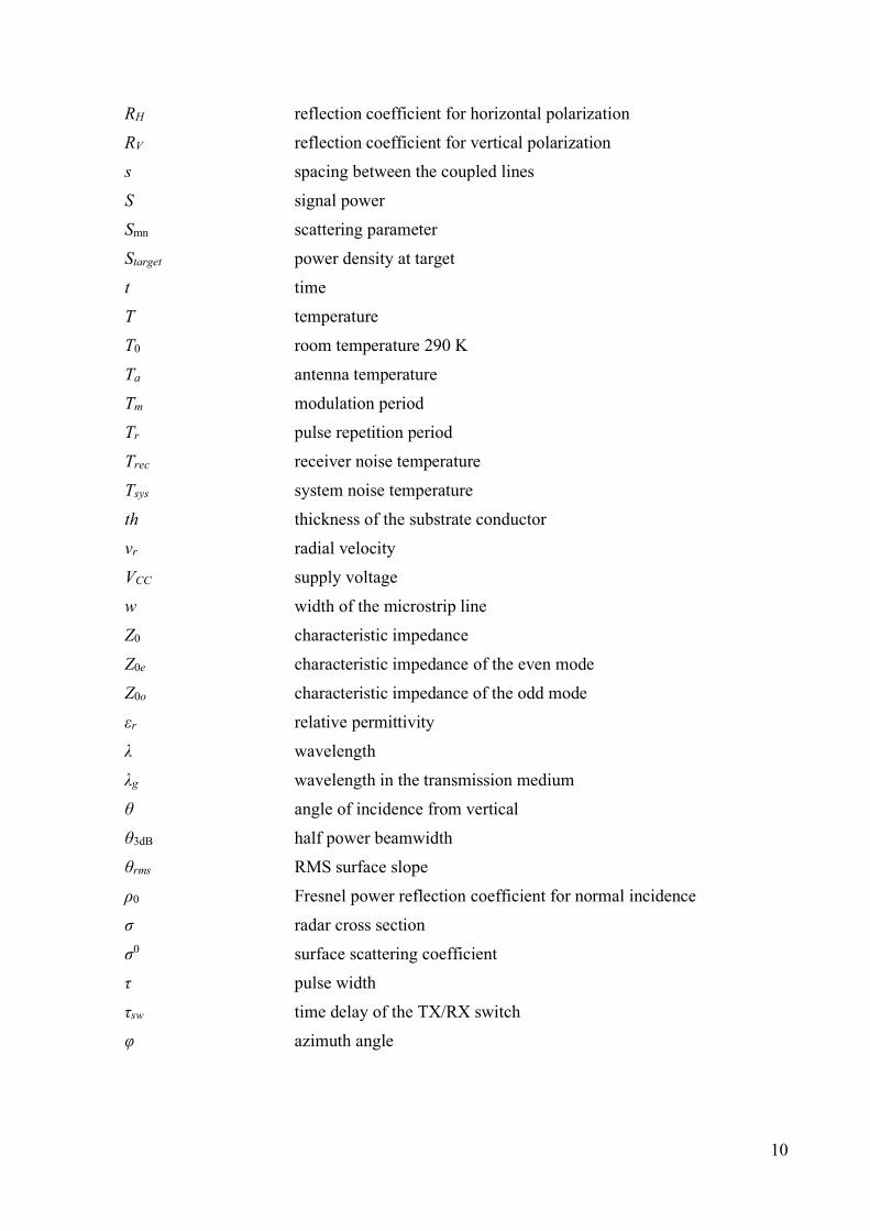
List of symbols
A area
Aeff antenna effective area
B bandwidth
BIF IF bandwidth
Bn noise bandwidth
c speed of light
C surface roughness parameter in Hagfors’ model in eq. (2.10 – 2.11);
coupling in dB in eq. (3.1) and (3.6)
D directivity in dB
f frequency
fb beat frequency
fD Doppler frequency
fIF intermediate frequency
fLO local oscillator frequency
fm modulation frequency
fr pulse repetition frequency
fRF radio frequency
F noise factor
G gain
G0 peak antenna gain
h thickness of the substrate
H altitude
k Boltzmann’s constant in eq. (2.24); coupling coefficient in eq. (3.4 –
3.6)
l length of the directional coupler
L loss
N noise power
NF noise figure
P power
P1dB output power at 1 dB compression
Pr received power
Pt transmit power
r radius
R distance to the target
10
RH reflection coefficient for horizontal polarization
RV reflection coefficient for vertical polarization
s spacing between the coupled lines
S signal power
Smn scattering parameter
Starget power density at target
t time
T temperature
T0 room temperature 290 K
Ta antenna temperature
Tm modulation period
Tr pulse repetition period
Trec receiver noise temperature
Tsys system noise temperature
th thickness of the substrate conductor
vr radial velocity
VCC supply voltage
w width of the microstrip line
Z0 characteristic impedance
Z0e characteristic impedance of the even mode
Z0o characteristic impedance of the odd mode
εr relative permittivity
λ wavelength
λg wavelength in the transmission medium
θ angle of incidence from vertical
θ3dB half power beamwidth
θrms RMS surface slope
ρ0 Fresnel power reflection coefficient for normal incidence
σ radar cross section
σ0 surface scattering coefficient
τ pulse width
τsw time delay of the TX/RX switch
φ azimuth angle
11
1. Introduction
1.1 Background
Humans have been exploring beyond the Earth’s atmosphere since 1957 when the first artificial
satellite, Sputnik 1, was launched to a low Earth orbit. Soon after that, during the 1960’s, we
already started sending spacecrafts to other celestial bodies (e.g. the Moon, other planets,
asteroids) for scientific missions.
A descent and landing system for a planetary exploration mission require a direct and reliable
measurement of a planet lander’s altitude. Some events (e.g. releasing the parachute, activation of
retro rockets) in an entry, descend and landing sequence are triggered based on the information
provided by the altimeter. There are basically two technological choices for measuring the ground
distance of the planetary lander, i.e. radar and laser radar (or LIDAR = light detection and ranging).
The working principle of both technologies is based on emitting electromagnetic waves towards
the target. The transmitted signals reflect from the target and return to the receiver. The distance
can then be calculated from the time it takes for the signal to travel to the target and back.
Altimeters based on both technologies have been successfully used in various exploration
missions. Due to the much longer wavelength compared to light, microwave radar signals
penetrate better through various media. Therefore, radar altimeters can measure through opaque
atmosphere, clouds, dust storms etc. The shorter wavelength of the LIDAR altimeter signal leads
to higher accuracy and resolution at short distances, but at the same time the radar altimeters have
longer operating distance due to the lower attenuation of the transmitted signal. One main
disadvantage of the radar technology compared to LIDAR is that the equipment dimensions
(especially the antennas) are increased due to the longer wavelength. As the radar and LIDAR
technologies differ from each other and excel in different operating conditions, they can be used
as redundant systems in the same mission. The European Space Agency is aiming at smaller
landers for the future exploration missions which impose excessive design constraints for mass,
size and available power of the lander. Therefore, also the altimeter sensor of the planet lander
must be minimized in terms of mass and power.
This thesis is based on the work done by Harp Technologies Ltd. within the European Space
Agency’s project “Assessment and Bread-boarding of a Planetary Altimeter (ABPA)”. The project
objective was to analyse, design and bread-board a hybrid planetary altimeter (i.e. radar and
LIDAR) for ESA’s exploration programme [1]. ESA has identified two mission scenarios which
need the altimeter: the Mars network science mission and the High Precision Lander for Mars.
Harp Technologies was responsible for the radar instrument and LusoSpace (Portugal) was
responsible for the LIDAR instrument of the hybrid altimeter. The author served as Chief Design
Engineer of the radar front-end module in this project. In addition to the radar front-end, antennas
for the radar altimeter were also developed by Harp Technologies. The central processing unit
(CPU) and power supply units (PSU) of the radar altimeter belong to the radar back-end and these
are not included in this thesis. The prime contractor of the project was EFACEC Electric Mobility
(Portugal) who was responsible for the detailed design of the radar back-end.
12
Author’s contribution was the system level design of the radar front-end, developing the RF
part of the radar front-end (excluding antennas and the IF part) and laboratory testing (including
the whole radar front-end with antennas). The RF part of the radar consists of VCO, PA, directional
coupler/isolator, LNA and mixer. M.Sc. Josu Uusitalo was responsible for the system level
modelling and simulations of the radar (including surface scattering modelling) and the design of
the antennas. Lic.Sc. (Tech) Kari Lehtinen was responsible for the detailed design of the IF part
and electronics (i.e. AGC, IF filter and VCO controller) of the radar front-end.
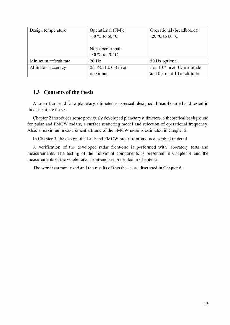
1.2 Requirements
The requirements of the altimeter are given in the Statement of Work (SoW) document [1] for
the project “Assessment and Bread-boarding of a Planetary Altimeter (ABPA)”. Some of the
requirements given in the SoW are fully applicable only for the final space hardware and the
performance requirements for the breadboard model were somewhat reduced. For example, the
mass and dimensions of the breadboard module were allowed to be larger than in the final Flight
Model (FM). However, the breadboard was required to comply with the functional requirements
and to have sufficient improvement potential for the later stages of the project. The main functional
requirements for the altimeter are presented in Table 1.
Table 1. The functional requirements for the altimeter.
Parameter Requirement Notes
Operational envelope for
altitude
3 km down to 10 m The altitude range in which
the altimeter shall supply data
to the GNC loop for action.
Ambiguity envelope for
altitude
7 km down to 3 km The altitude range in which
the altimeter shall supply data
but the GNC loop is passive.
Maximum G-load 40 g To survive Earth launch and
the Mars entry and parachute
deployment.
Maximum mass Breadboard: 1.68 kg
FM: 1 kg
Including electronics box and
the required antennas.
Consequently, the target mass
for the radar front-end was set
to 0.67 kg
Maximum dimensions Breadboard: 15 x 13 x 10 cm3
FM: 15 x 10 x 10 cm3
Consequently, the mechanical
envelope target of 15 x 10 x 7
cm3 was set for the radar
front-end.
Maximum power
consumption
5 W 5 W for the entire altimeter
assembly. The target for the
radar front-end was set to 2.5
W.
13
Design temperature Operational (FM):
-40 ºC to 60 ºC
Non-operational:
-50 ºC to 70 ºC
Operational (breadboard):
-20 ºC to 60 ºC
Minimum refresh rate 20 Hz 50 Hz optional
Altitude inaccuracy 0.33% H ± 0.8 m at
maximum
i.e., 10.7 m at 3 km altitude
and 0.8 m at 10 m altitude
1.3 Contents of the thesis
A radar front-end for a planetary altimeter is assessed, designed, bread-boarded and tested in
this Licentiate thesis.
Chapter 2 introduces some previously developed planetary altimeters, a theoretical background
for pulse and FMCW radars, a surface scattering model and selection of operational frequency.
Also, a maximum measurement altitude of the FMCW radar is estimated in Chapter 2.
In Chapter 3, the design of a Ku-band FMCW radar front-end is described in detail.
A verification of the developed radar front-end is performed with laboratory tests and
measurements. The testing of the individual components is presented in Chapter 4 and the
measurements of the whole radar front-end are presented in Chapter 5.
The work is summarized and the results of this thesis are discussed in Chapter 6.
14
2. Planetary radar altimeters
2.1 Radar applications
The history of radar can be traced back to James Clerk Maxwell’s work on electromagnetism.
In 1865, Maxwell published his theory “A Dynamical Theory of the Electromagnetic Field”, which
implied that electromagnetic fields travelled through space as waves with the speed of light.
Maxwell’s mathematical theory was proved in 1887, when Heinrich Hertz discovered the
existence of the electromagnetic waves with his series of experiments. This gave basis for many
later inventions, such as television, radio and radar.
The first idea of radar came soon after, in 1904, when German engineer Christian Hülsmeyer
patented and built a device to detect ships. The device was rather simple, because the device,
“telemobiloscope”, was only able to detect the presence of the ships, but not their accurate range
[2].
The radar technology advanced significantly during the World War II, when different radar
devices were developed independently in many countries, e.g. in the UK, USA, Germany, France,
Soviet Union and Japan. The most important early military application was to notify and detect
the range of approaching hostile aircrafts. Hence the word itself, radar, is an acronym for “Radio
Detection and Ranging”. By the end of the war, hundreds of different radar systems had been
developed.
Since the early military applications, the use of radar technology has widened to numerous
fields. The non-military applications include: air and terrestrial traffic control, vehicle anti-
collision systems, autonomous vehicles, navigation, surveillance systems, meteorological
monitoring, geological observations, altimetry etc. Due to the development in electronics and
signal processing techniques, the use of radar applications has entered our everyday life. The
development will not stop, the radar systems will become smaller and cheaper in the future, and
as a result can be used in various new areas.
Obviously, radar systems have also been used in space exploration programs since the
beginning. Radar altimetry is basically a technique for measuring height. The measurement also
yields valuable other information that can be used in many applications. The first Earth observation
satellites were launched during 1970s (Skylab, GEOS3 and Seasat) and since then, precise satellite
altimetry missions have changed the way we view Earth. Currently, multiple satellites are mapping
the surface of Earth and providing scientific information for various applications. Parameters that
can be inferred from radar altimeter measurements include sea surface height, wind speeds, ocean
topography, land and sea ice, geoid modeling etc. The information provided by satellites is the key
asset for accurate weather forecasts and studying the climate change. The ESA publication “Radar
altimetry tutorial” [3] gives thorough overview of past, current and future satellite altimetry
missions and their applications.
This thesis focuses on one important radar altimeter application, i.e. landing safely on a
planetary surface.
15
2.2 Reference altimeters with space heritage
Since the 1960s, several successful altimeter aided landings on the Moon, Mars, Venus and
Titan have been performed. Considering only radar altimeters, both pulse and frequency
modulated continuous wave (FMCW) radar concepts have been used in the planetary altimeters.
The current activity has strict requirements for the power consumption, mass and measurement
range. In order to initially estimate the performance of the pulse and FMCW radar technologies,
the radar altimeters that have space heritage from the 1990s and 2000s were surveyed.
2.2.1 HG8500 pulse radar
Honeywell HG8500 pulse radar altimeter has been applied on successful Pathfinder and Mars
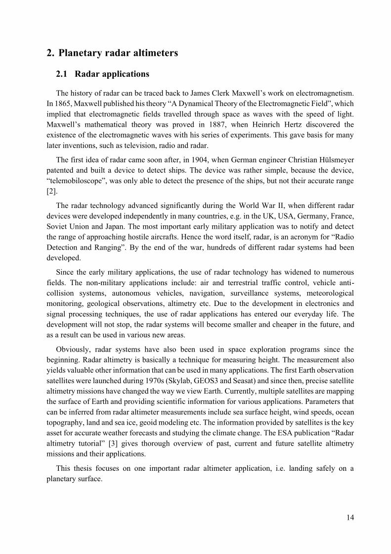
Exploration Rovers (MER) missions. A photograph of the Honeywell HG8500 pulse radar is
shown in Figure 1 and the main specifications are presented in Table 2.
The operational center frequency of the HG8500 radar is 4.3 GHz and the specified altitude
range is 0 – 2500 m. The radar utilizes antennas with rather wide beamwidths (50°), and therefore
an obvious solution to improve the maximum range would be to use higher gain antennas. The
maximum unambiguous range can be estimated from the specified pulse repetition frequency (PRF
= 25 kHz). The maximum unambiguous range for the HG8500 is approximately 6 km, and thus it
fulfills the requirement (3 km) for the current application. However, the specified maximum power
consumption (16 W) largely exceeds the current requirement of 2.5 W for the radar front-end. In
order to fulfill the specified requirement, the transmit power of the radar must be reduced.
Obviously, this would lead to the maximum range reduction at the same time.
Figure 1. Honeywell HG8500 series pulse radar altimeter [4].
16
Table 2. Key parameters of Honeywell HG8500 pulse radar altimeter [1][4].
Parameter Value
Altitude range 0 – 2500 m
Altitude accuracy ± (0.9 m + 3%) analog
± (0.9 m + 1%) digital
Frequency 4300 ± 10 MHz
Power consumption max. 16 W
Transmit power 5 W peak
Pulse length 30/225 ns
Pulse repetition frequency (PRF) 25 kHz
Size 86 mm x 86 mm x 142 mm
Mass 1.4 kg (including antennas)
Number of antennas 2
Antenna beamwidth 50°
Antenna gain 9.5 dBi
Antenna size 89 mm x 89 mm
2.2.2 Terminal Descent Sensor
More recent example of the pulse radar is the Terminal Descent Sensor (TDS) developed for
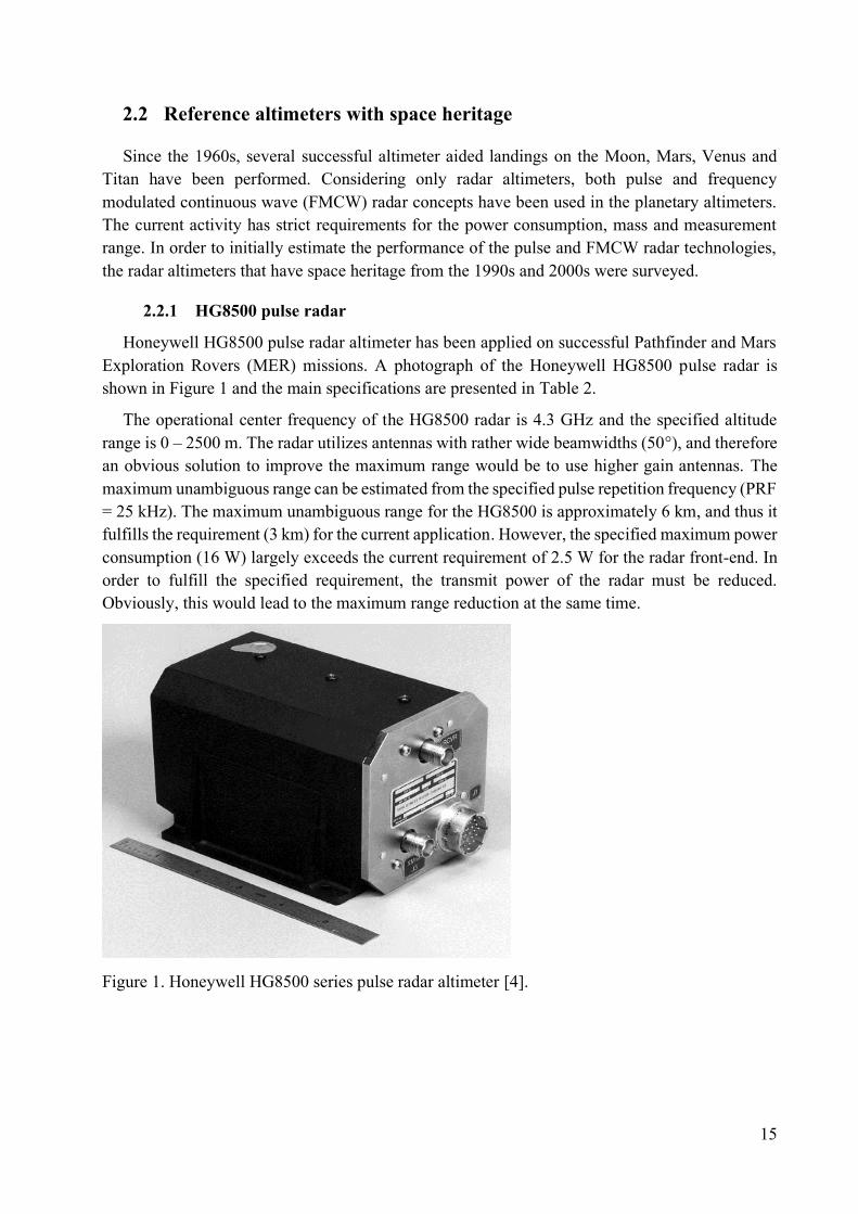
the Mars Science Laboratory mission. This planetary lander successfully delivered Curiosity rover
on Mars, in the year 2012. A hardware illustration of the TDS is shown in Figure 2. Some data on
the TDS has been published in the literature [5], and the main specifications are given in Table 3.
The TDS has the center frequency of 35.75 GHz and the altitude range of 10 – 3500 m. The
radar contains six unique antennas for the accurate acquisition of velocity and altitude. The power
consumption of the whole system is not given, but it largely exceeds the current requirement as
the transmit power per antenna is 2 W.
Figure 2. Hardware illustration of the TDS [5].
17
Table 3. Key parameters of the TDS pulse radar.
Parameter Value
Altitude range 10 – 3500 m
Altitude accuracy 2%
Frequency 35.75 GHz
Transmit power 2 W peak (per antenna)
Range of pulse lengths 4 – 16000 ns
Range of pulse repetition intervals 75 – 250 μs
Number of antennas 6
Antenna beamwidth < 3°
2.2.3 Huygens FMCW radar
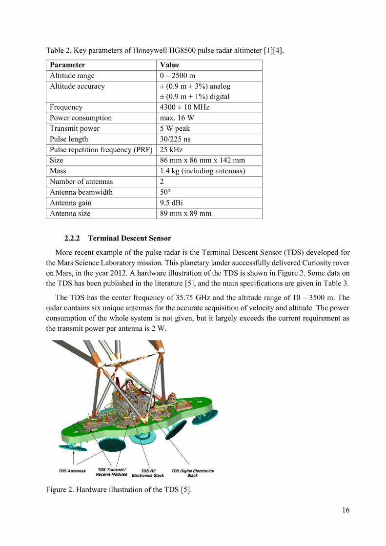
FMCW radars have also a strong heritage in space missions. The Huygens radar altimeter
developed by Ylinen Electronics, Finland, demonstrated reliable operation when landing on Saturn
moon, Titan, in 2005. A photograph of the Huygens FMCW radar altimeter with the most of the
microwave components visible is shown in Figure 3. As can be seen in the photograph, a level of
integration is rather low. Especially, a voltage controlled oscillator (VCO) and filters consume a
lot of space. Significant reduction of size and mass would be possible with modern microwave
components.
Figure 3. Huygens FMCW radar altimeter, showing antennas and opened microwave compartment
[6].
18
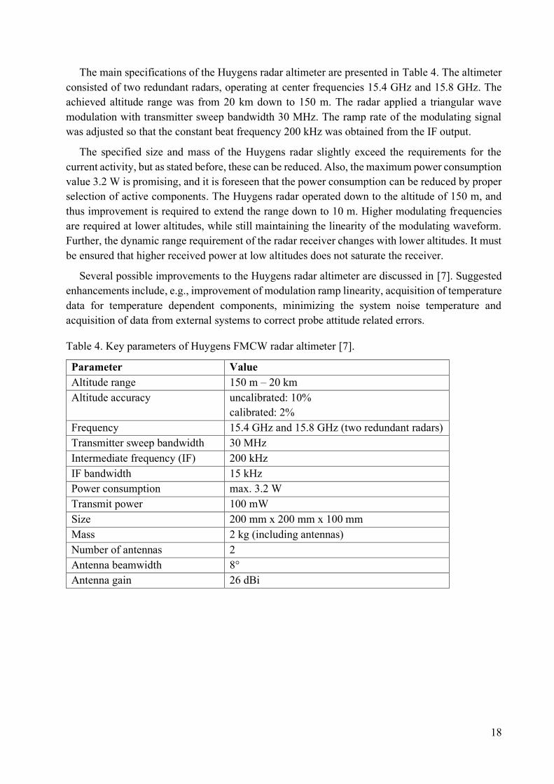
The main specifications of the Huygens radar altimeter are presented in Table 4. The altimeter
consisted of two redundant radars, operating at center frequencies 15.4 GHz and 15.8 GHz. The
achieved altitude range was from 20 km down to 150 m. The radar applied a triangular wave
modulation with transmitter sweep bandwidth 30 MHz. The ramp rate of the modulating signal
was adjusted so that the constant beat frequency 200 kHz was obtained from the IF output.
The specified size and mass of the Huygens radar slightly exceed the requirements for the
current activity, but as stated before, these can be reduced. Also, the maximum power consumption
value 3.2 W is promising, and it is foreseen that the power consumption can be reduced by proper
selection of active components. The Huygens radar operated down to the altitude of 150 m, and
thus improvement is required to extend the range down to 10 m. Higher modulating frequencies
are required at lower altitudes, while still maintaining the linearity of the modulating waveform.
Further, the dynamic range requirement of the radar receiver changes with lower altitudes. It must
be ensured that higher received power at low altitudes does not saturate the receiver.
Several possible improvements to the Huygens radar altimeter are discussed in [7]. Suggested
enhancements include, e.g., improvement of modulation ramp linearity, acquisition of temperature
data for temperature dependent components, minimizing the system noise temperature and
acquisition of data from external systems to correct probe attitude related errors.
Table 4. Key parameters of Huygens FMCW radar altimeter [7].
Parameter Value
Altitude range 150 m – 20 km
Altitude accuracy uncalibrated: 10%
calibrated: 2%
Frequency 15.4 GHz and 15.8 GHz (two redundant radars)
Transmitter sweep bandwidth 30 MHz
Intermediate frequency (IF) 200 kHz
IF bandwidth 15 kHz
Power consumption max. 3.2 W
Transmit power 100 mW
Size 200 mm x 200 mm x 100 mm
Mass 2 kg (including antennas)
Number of antennas 2
Antenna beamwidth 8°
Antenna gain 26 dBi
19
2.3 Pulse and FMCW radar concepts
2.3.1 Basic principle of pulse radar
A simple method to extract a distance to a target surface is to transmit a train of RF energy
pulses towards the target. A part of the signal is reflected back and received with the radar system.
As the electromagnetic signal travels with the speed of light c, the range can be determined from
the time delay Δt between the transmitted and received pulses. Assuming the received power is
high enough to be detected, the target range R is simply
𝑅 =𝑐Δ𝑡
2, (2.1)
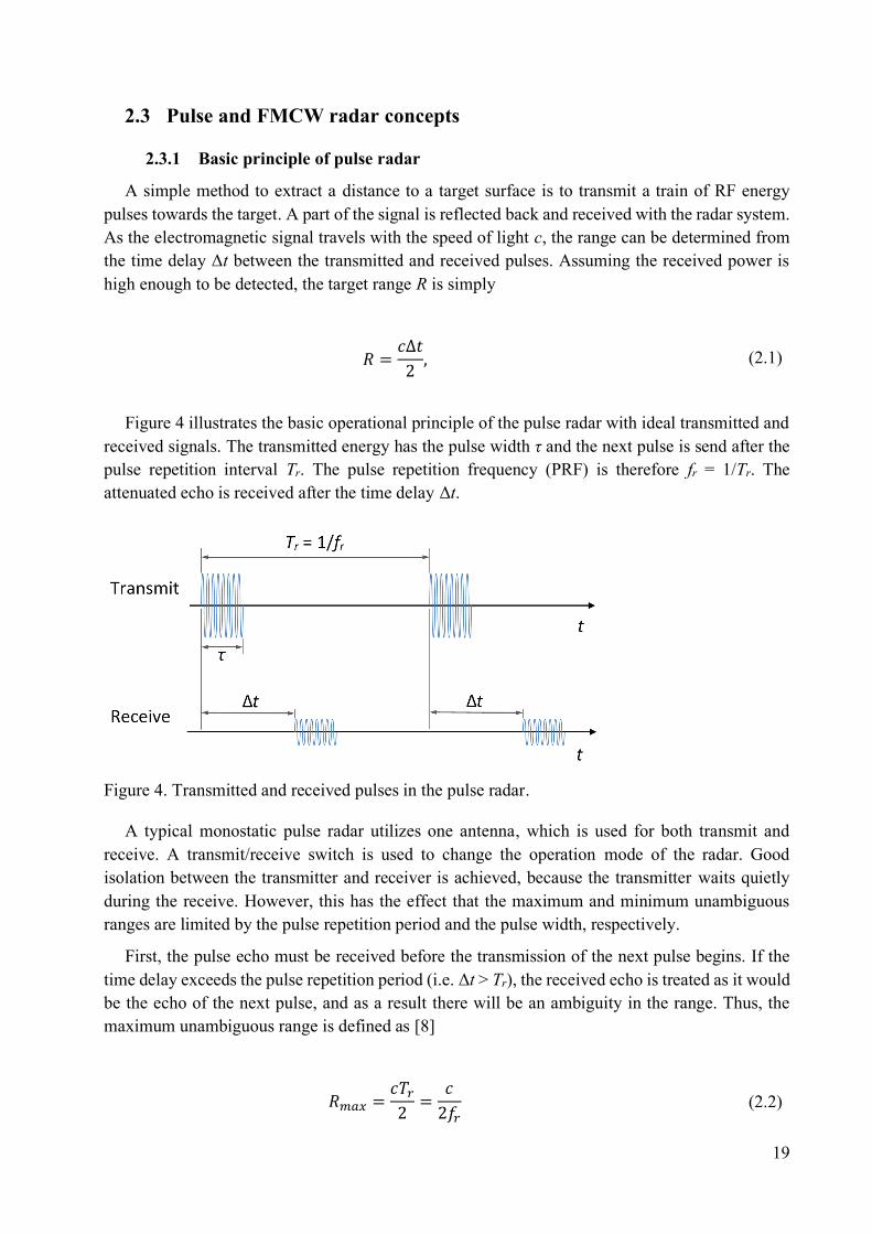
Figure 4 illustrates the basic operational principle of the pulse radar with ideal transmitted and
received signals. The transmitted energy has the pulse width τ and the next pulse is send after the
pulse repetition interval Tr. The pulse repetition frequency (PRF) is therefore fr = 1/Tr. The
attenuated echo is received after the time delay Δt.
Figure 4. Transmitted and received pulses in the pulse radar.
A typical monostatic pulse radar utilizes one antenna, which is used for both transmit and
receive. A transmit/receive switch is used to change the operation mode of the radar. Good
isolation between the transmitter and receiver is achieved, because the transmitter waits quietly
during the receive. However, this has the effect that the maximum and minimum unambiguous
ranges are limited by the pulse repetition period and the pulse width, respectively.
First, the pulse echo must be received before the transmission of the next pulse begins. If the
time delay exceeds the pulse repetition period (i.e. Δt > Tr), the received echo is treated as it would
be the echo of the next pulse, and as a result there will be an ambiguity in the range. Thus, the
maximum unambiguous range is defined as [8]
𝑅𝑚𝑎𝑥 =𝑐𝑇𝑟
2=
𝑐
2𝑓𝑟 (2.2)
20
Secondly, the pulse echo cannot be processed before the full pulse has been transmitted. The
minimum range is therefore limited by the pulse width. In practice, the transmit/receive switch
cannot change its state instantaneously, and the time delay of the switch, τsw, must be included
when defining the minimum unambiguous range. Thus, the minimum unambiguous range is
𝑅𝑚𝑖𝑛 =𝑐(𝜏 + 𝜏𝑠𝑤)
2 (2.3)
Solving the PRF from equation (2.2) for the current planetary altimeter (the required maximum
unambiguous range Rmax = 3 km) leads to the requirement fr < 50 kHz. Adopting the maximum
value fr = 50 kHz is beneficial, because it maximizes the number of pulses received during the
specified refresh period (i.e. 1/(20 Hz) = 50 ms). The effective signal-to-noise ratio of the received
echo can be improved by using pulse integration in the radar receiver. The specified maximum
measurement altitude of the planetary altimeter is 7 km. The chosen fr = 50 kHz will lead to range
ambiguities at altitudes above 3 km, but the lander is required to resolve this by the use of timing,
acceleration or other supporting data. The main design challenge of the pulse radar altimeter is to
achieve sufficient signal-to-noise ratio at high altitudes, given that the available transmit power is
very limited. The total power consumption of the radar front-end is required to be less than 2.5 W,
which leaves very small amount of power for the actual transmitted pulses.
Another design challenge for the pulse radar altimeter is established by the required minimum
operational altitude, Rmin = 10 m. First assuming an ideal transmit/receive switch with τsw = 0, and
then solving equation (2.3) leads to the required pulse width τ < 7 ns at the range Rmin = 10 m.
State-of-the-art PIN diode switches are able to achieve switching times τsw < 10 ns. Introducing
realistic switching time to equation (2.3) leaves no room for the pulse width. Thus, the simple
pulse radar concept based on one transmit/receive antenna is not applicable for this planetary
altimeter, if the switching time is higher than approximately 2 ns. In that case, simultaneous
transmission and receiving will be necessary, which creates constraints for the required
transmitter/receiver isolation.
Very short pulses required at low altitudes introduce also a problem at high altitudes.
Detectability of the signal depends on the received pulse energy and noise power [9]. Thus, to
improve the signal-to-noise ratio (SNR) at high altitudes, the radar average transmitted power must
be increased by increasing the pulse width. Therefore, the pulse radar for the current application
would require adjustable pulse width.
Another method to improve the maximum range is to utilize pulse compression techniques. In
the pulse compression technique, the frequency or phase of the transmitted pulse is swept (typically
linearly) during the pulse. The bandwidth of the pulse increases compared to the bandwidth of
unmodulated pulse of the same duration. A matched filter is used in the receiver to compress the
pulse to a shorter length. Thus, the signal-to-noise ratio is improved. However, the pulse
compression technique increases the radar design complexity compared to the ordinary pulse
radar.
21
Using the pulse radar concept for the current planetary altimeter would create several design
challenges due to the stringent performance requirements. Therefore, another solution is preferred.
2.3.2 Basic principle of FMCW radar
Unmodulated continuous wave (CW) radars utilize pure sinusoidal waveforms. They can be
used to extract target radial velocity, because the center frequency of echoes from moving targets
will be shifted by the Doppler frequency, fD. The advantage of the CW radar is its simplicity as the
Doppler frequency shift is determined by [9]
𝑓𝐷 =2𝑣𝑟𝑓0
𝑐, (2.4)
where vr is the radial velocity difference between the target and the radar and f0 is the transmitted
frequency. The Doppler frequency shift is positive for approaching targets and negative for
receding targets.
However, the CW radar is fundamentally incapable of determining the range of the target. In
order to measure the range, the transmit waveform must be modulated. A common technique is to
frequency modulate a microwave oscillator, which serves as both transmitter and local oscillator
of the radar. These radars are called frequency modulated continuous wave (FMCW) radars. The
modulating waveform may be a linear sawtooth, triangular, sinusoidal or some other form.
Using triangular modulation is convenient in the radar altimeters, because the Doppler shift
caused by the moving target can be averaged out. The frequency-time relationships of the linear
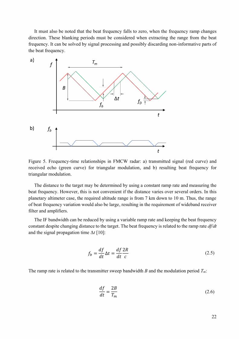
triangular wave modulation are shown in Figure 5. The red curve in Figure 5a is the transmitted
frequency with rising and falling ramp. The received signal (shown in green color) has a similar
form. However, the received signal is delayed by the signal propagation time, Δt, resulting in the
difference or beat frequency fb between the transmitted and received signals. If the target is
approaching (which is the case for planetary landers), the received frequency is also shifted higher
by the Doppler frequency fD. The Doppler shift shown in the figure is largely exaggerated for
representation purposes.
The beat frequency can be obtained by mixing the transmitted and received signals, and the
result is shown in Figure 5b. During the rising ramp, the Doppler frequency produced by the
approaching target decreases the resulting beat frequency, and during the falling ramp the Doppler
frequency increases the beat frequency. Moreover, the Doppler frequency is somewhat higher
when the transmitted signal is above its center frequency and lower when the transmitted signal is
below its center frequency. However, the effect is so small that this lack of parallelism between
the transmitted and received signals is not shown in Figure 5a. If target radial velocity does not
change drastically, the Doppler shift can be cancelled by averaging the beat frequency over the
modulation period Tm. The maximum anticipated velocity, and thus Doppler frequency, of the
target must be taken into account when deciding the bandwidth for the IF filter. The IF bandwidth
must be at least twice the Doppler frequency in order to keep the received beat frequency in the
band during the modulation period.
22
It must also be noted that the beat frequency falls to zero, when the frequency ramp changes
direction. These blanking periods must be considered when extracting the range from the beat
frequency. It can be solved by signal processing and possibly discarding non-informative parts of
the beat frequency.
Figure 5. Frequency-time relationships in FMCW radar: a) transmitted signal (red curve) and
received echo (green curve) for triangular modulation, and b) resulting beat frequency for
triangular modulation.
The distance to the target may be determined by using a constant ramp rate and measuring the
beat frequency. However, this is not convenient if the distance varies over several orders. In this
planetary altimeter case, the required altitude range is from 7 km down to 10 m. Thus, the range
of beat frequency variation would also be large, resulting in the requirement of wideband receiver
filter and amplifiers.
The IF bandwidth can be reduced by using a variable ramp rate and keeping the beat frequency
constant despite changing distance to the target. The beat frequency is related to the ramp rate df/dt
and the signal propagation time Δt [10]:
𝑓𝑏 =𝑑𝑓
𝑑𝑡Δ𝑡 =
𝑑𝑓
𝑑𝑡
2𝑅
𝑐 (2.5)
The ramp rate is related to the transmitter sweep bandwidth B and the modulation period Tm:
𝑑𝑓
𝑑𝑡=
2𝐵
𝑇𝑚 (2.6)
23
The modulation frequency fm is the inverse of the modulation period Tm:
𝑓𝑚 =1
𝑇𝑚=
𝑓𝑏
2𝐵Δ𝑡 (2.7)
Now, using equations (2.5) – (2.7), the distance R to the target can be solved:
𝑅 =𝑓𝑏𝑐
2𝑑𝑓𝑑𝑡
=𝑓𝑏𝑐
4𝑓𝑚𝐵 (2.8)
The requirement for the relative range accuracy given in Table 1 is 0.33% ± 0.8 mm, which is
1-sigma accuracy. When solving the range R from equation (2.8), the accuracy of the whole range
measurement depends on the accuracy of three parameters, i.e. the measured beat frequency fb, the
transmitter sweep bandwidth B and the modulation frequency fm.
The frequency change in the transmitted radar signal is achieved by sweeping a tuning voltage
of a voltage controlled oscillator (VCO) with certain modulation frequency. The modulation
frequency fm can be controlled very accurately by using a digital microcontroller. However, the
VCO output frequencies are generated with analogue electronics which have a limited accuracy.
Therefore, the resulting VCO output sweep bandwidth B has uncertainty ΔB. It is also possible
that the sweep bandwidth depends on the temperature. Consequently, as the sweep bandwidth
cannot be controlled accurately, it must be characterized and the uncertainty have to be taken into
account in the range calculation.
Another parameter which affects the range calculation is the measured beat frequency fb.
Ideally, the beat frequency is kept constant in the servo-type FMCW radar. In practice, the beat
frequency has certain deviation, Δfb, which has an influence on the range accuracy. There are many
non-idealities which affect the beat frequency deviation. First, a sufficient signal-to-noise ratio
(SNR) is required to extract the beat frequency from the noise. Poor signal-to-noise ratio affects
the accuracy of the beat frequency especially at high altitudes. The second non-ideality is related
to the target geometry. The target is a continuous ground surface, which causes randomly
fluctuating echo in both amplitude and phase. The spectrum of the echo is wider than for the ideal
point-like target, and therefore the range retrieval will get more inaccurate. Also, an error is
introduced in the measured beat frequency, if the phase of the signal is not solely determined by
the signal delay. Thus, the stability of the transmitted signal (sweep linearity and phase noise) also
affect the accuracy of the beat frequency.
Thus, two main contributors to the calculated range error are the accuracy of the transmitter
sweep bandwidth and the accuracy of the beat frequency. These error sources are not correlated,
and thus the relative range accuracy can be expressed as:
24
Δ𝑅
𝑅= √(
Δ𝐵
𝐵)
2
+ (Δ𝑓𝑏
𝑓𝑏)
2
(2.9)
The required relative range accuracy ΔR/R is 0.33%. The design goals for the radar can be
established by allocating the total requirement equally between the two contributors (i.e. 0.23%
for both).
The main design concern in FMCW radars is transmitter/receiver isolation. Because the
transmitter is operating constantly, the direct leakage to the receiver can obscure weak target
echoes. The problem is usually tackled by using separate antennas for the transmitter and receiver.
If the geometry permits, the antennas can be widely separated to achieve good isolation.
The FMCW radar concept is technically simpler than the pulse radar. Given that the available
transmit power is limited, the anticipated maximum measurement distance is also greater due to
the continuous transmission.
2.4 Surface scattering model
A radar backscattering from a surface can be estimated with a variety of methods. One method
to describe the terrain scattering is Hagfors’ model [11]. The Hagfors model assumes a Gaussian
distribution of surface heights, where the surface is described by the surface roughness parameter
C and the Fresnel normal reflection coefficient ρ0. The assumptions for the surface-slope
distributions and correlation functions in the Hagfors model have been criticized, but the model is
still widely used in planetary applications. The Hagfors model usually shows good agreement with
near-nadir radar measurements of planetary objects. In this model the surface scattering
coefficient σ0 with different angles of incidence θ has the form [12]
𝜎0(𝜃) =𝐶𝜌0
2(cos4𝜃 + 𝐶sin2𝜃)−3/2 (2.10)
The surface roughness parameter C in the model is accepted to be related to the root-mean-
square (RMS) of the surface slope distribution θrms [13]
𝐶 = tan−2𝜃𝑟𝑚𝑠 (2.11)
Any arbitrary electromagnetic wave can be divided into horizontal and vertical polarization
components. Horizontal polarization is also called TE-polarization as the electric field of the
incident wave is perpendicular to the normal vector. In vertical polarization or TM-polarization,
the magnetic field component is perpendicular to the normal vector. Assuming a non-magnetic
surface material, Fresnel amplitude reflection coefficients for horizontal and vertical polarizations
are [14]
25
𝑅𝐻 =cos 𝜃 − √𝜀𝑟 − sin2𝜃
cos 𝜃 + √𝜀𝑟 − sin2𝜃 (2.12)
𝑅𝑉 =𝜀𝑟 cos 𝜃 − √𝜀𝑟 − sin2𝜃
𝜀𝑟 cos 𝜃 + √𝜀𝑟 − sin2𝜃 (2.13)
The power reflection coefficient for the normal angle of incidence (i.e. θ = 0°) ρ0 can now be
retrieved from
𝜌0 = |1 − √𝜀𝑟
1 + √𝜀𝑟|
2
, (2.14)
where εr is the relative permittivity of the surface material.
In order to estimate the scattering coefficient σ0 for the surface of Mars, estimates for the
relative permittivity εr and the RMS surface slope θrms are required. Some measurement data on εr
and θrms for Mars have been published [14] [15]. According to [14], bistatic radar experiments
were conducted during years 1977-78 by the Viking orbiter spacecraft. The results for Hellas Basin
and the equatorial region showed the RMS surface slope to be θrms = 4 – 5°. The estimates for the
relative permittivity ranged from εr = 1.5 in certain parts of the north polar region to εr = 4.0 in
Syrtis Major. Syrtis Major is also the smoothest region in Mars, where areas with θrms < 0.25° have
been detected. Additionally, [14] reports that generally for Mars, plains are smoothest (θrms < 2°)
and sand dunes are roughest (3.5 < θrms < 7°).
More recent measurements of the surface roughness were performed by the Mars Global
Surveyor spacecraft. According to [15], the RMS slopes show an average of θrms = 3 – 10° in the
southern highlands and θrms = 0.2 – 0.8° in the northern lowlands.
Based on the above reference data, the surface scattering coefficient σ0 for Mars can be
estimated with equation (2.10). Three landing scenarios for poorly, typical and highly reflective
surfaces are shown in Figure 6. The poorly reflective surface with εr = 1.5 and θrms = 10° is the
scenario, where the landing occurs at the highlands. It is questionable if the relative permittivity
of the surface has the lowest value occurring at the same time with steep slopes, because the low
permittivity usually requires that the surface material is not dense. Therefore, this poorly reflective
situation is considered as the worst case scenario. The best case scenario is landing to Syrtis Major,
which is flat and has the highest reported relative permittivity. The highly reflective case in the
graph is calculated with values εr = 4.0 and θrms = 0.5°. The third graph for the scattering coefficient
is the scenario, where the surface parameters are considered to be close to typical (εr = 3.0 and θrms
= 5°). This typical case is used as a reference, when estimating the return power with the radar
equation. When the incident angle of the antenna beam is close to vertical, the surface scattering
coefficient is approximately σ0 = 6 dB in the typical case. The attitude of the lander (and thus the
incident angle of the antenna beam) is assumed to remain in the range 0 – 10° during the operation
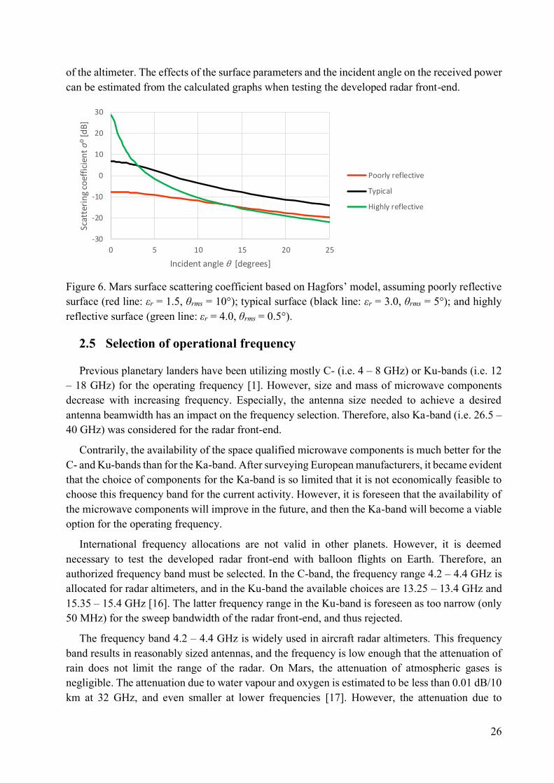
26
of the altimeter. The effects of the surface parameters and the incident angle on the received power
can be estimated from the calculated graphs when testing the developed radar front-end.
Figure 6. Mars surface scattering coefficient based on Hagfors’ model, assuming poorly reflective
surface (red line: εr = 1.5, θrms = 10°); typical surface (black line: εr = 3.0, θrms = 5°); and highly
reflective surface (green line: εr = 4.0, θrms = 0.5°).
2.5 Selection of operational frequency
Previous planetary landers have been utilizing mostly C- (i.e. 4 – 8 GHz) or Ku-bands (i.e. 12
– 18 GHz) for the operating frequency [1]. However, size and mass of microwave components
decrease with increasing frequency. Especially, the antenna size needed to achieve a desired
antenna beamwidth has an impact on the frequency selection. Therefore, also Ka-band (i.e. 26.5 –
40 GHz) was considered for the radar front-end.
Contrarily, the availability of the space qualified microwave components is much better for the
C- and Ku-bands than for the Ka-band. After surveying European manufacturers, it became evident
that the choice of components for the Ka-band is so limited that it is not economically feasible to
choose this frequency band for the current activity. However, it is foreseen that the availability of
the microwave components will improve in the future, and then the Ka-band will become a viable
option for the operating frequency.
International frequency allocations are not valid in other planets. However, it is deemed
necessary to test the developed radar front-end with balloon flights on Earth. Therefore, an
authorized frequency band must be selected. In the C-band, the frequency range 4.2 – 4.4 GHz is
allocated for radar altimeters, and in the Ku-band the available choices are 13.25 – 13.4 GHz and
15.35 – 15.4 GHz [16]. The latter frequency range in the Ku-band is foreseen as too narrow (only
50 MHz) for the sweep bandwidth of the radar front-end, and thus rejected.
The frequency band 4.2 – 4.4 GHz is widely used in aircraft radar altimeters. This frequency
band results in reasonably sized antennas, and the frequency is low enough that the attenuation of
rain does not limit the range of the radar. On Mars, the attenuation of atmospheric gases is
negligible. The attenuation due to water vapour and oxygen is estimated to be less than 0.01 dB/10
km at 32 GHz, and even smaller at lower frequencies [17]. However, the attenuation due to
-30
-20
-10
0
10
20
30
0 5 10 15 20 25
Scat
teri
ng
coef
fici
ent σ⁰
[dB
]
Incident angle θ [degrees]
Hagfors surface scattering
Poorly reflective
Typical
Highly reflective
27
relatively common dust storms has to be considered. According to [17], the attenuation Ldust = 3
dB is the worst case estimate for 32 GHz signals over the 10 km dust cloud. The attenuation at
lower frequencies is achieved by scaling with 1/λ. Scaling to 4.3 GHz and 13.3 GHz leads to the
worst case attenuations Ldust = 0.04 dB/km and Ldust = 0.12 dB/km, respectively. The attenuation
of the severe dust storm is so low for both frequency choices that a definite conclusion for the
selection cannot be drawn.
Separate antennas for the transmit and receive are required for the FMCW radar. The exact
diameter of the planetary lander is not yet known in the breadboarding phase of the project, but
the diameter is estimated to be approximately 60 cm. Based on the preliminary analysis for the
maximum measurement altitude and the accuracy of the altimeter, the half-power beamwidth θ3dB
of the antennas must be less than 10° to fulfill the specifications. The diameter of the antennas can
initially be estimated from θ3dB ≃ λ/d [18]. Thus, at 4.3 GHz the antenna diameter is d = 40 cm
and at 13.3 GHz the antenna diameter is d = 13 cm, if the half-power beamwidth is 10°. It can be
concluded that the frequency 4.3 GHz leads to too large antenna size in this application. The choice
of the operational center frequency is therefore 13.3 GHz.
2.6 Estimated range of the radar altimeter
The received power Pr is required for the calculation of the signal-to-noise ratio and estimated
maximum range of the radar. If the transmitted power is Pt and the gain of the transmit antenna is
G, the power density at the target distance R is obtained from [19]
𝑆𝑡𝑎𝑟𝑔𝑒𝑡 =𝑃𝑡𝐺
4𝜋𝑅2 (2.15)
The surface of the target reradiates the intercepted electromagnetic energy in all directions. The
radar cross section σ of the target is defined as the ratio of the reflected power in the direction of
the radar to the incident power density. The radar cross section depends on many parameters, such
as transmitted frequency, target geometry, orientation and material. The power received by the
radar is then
𝑃𝑟 =𝑃𝑡𝐺
4𝜋𝑅2
𝜎
4𝜋𝑅2𝐴𝑒𝑓𝑓 , (2.16)
where Aeff is the effective area of the receiving antenna. The effective aperture of the antenna is
related to its gain by
𝐴𝑒𝑓𝑓 =𝜆2
4𝜋𝐺 (2.17)
Inserting equation (2.17) to (2.16) leads to the simplest form of the radar equation for monostatic
radars:
28
𝑃𝑟 =𝑃𝑡𝐺2𝜆2𝜎
(4𝜋)3𝑅4 (2.18)
Equation (2.18) is not accurate enough for predicting the range in practical situations. This
overly simplified radar equation neglects various losses (such as atmospheric attenuation and
system losses). Moreover, the target cross section and the minimum detectable signals are
statistical in nature, and the received signals are corrupted with noise.
Radar altimeters transmit signals towards the ground surface. The ground surface is a
distributed target and the backscattered signal is caused by various scatterers within the area
illuminated by the radar. The target radar cross section is given by
𝜎 = 𝜎0𝐴 , (2.19)
where σ0 is the backscattering coefficient (or the normalized reflectivity per unit area) and A is the
illuminated surface area.
The received power can be expressed as a surface integral over the illuminated area. Thus, the
area-extensive form of the radar equation is [20]
𝑃𝑟 =𝑃𝑡𝜆2
(4𝜋)3∫
𝐺2𝜎0
𝑅4
𝐴
𝑑𝐴
(2.20)
Equation (2.20) assumes a uniformly illuminated target area. However, the antenna radiation
pattern is not uniform in practice, and therefore the antenna beam must be approximated when the
actual shape is not yet known. A Gaussian, circularly symmetric antenna pattern is assumed for
the initial range estimation. The function for the Gaussian antenna pattern is [21]
𝐺(𝜃) = 𝐺0𝑒−2.773
𝜃2
𝜃3dB2
, (2.21)
where G0 is the peak antenna gain and θ3dB is the half-power beamwidth.
The geometry associated with equation (2.20) is shown in Figure 7. The surface area element
dA inside the illuminated area can be expressed in spherical coordinates:
𝑑𝐴 = 𝑅 sin 𝜃𝑅
cos 𝜃𝑑𝜃𝑑𝜑 = 𝑅2 tan 𝜃 𝑑𝜃𝑑𝜑 (2.22)
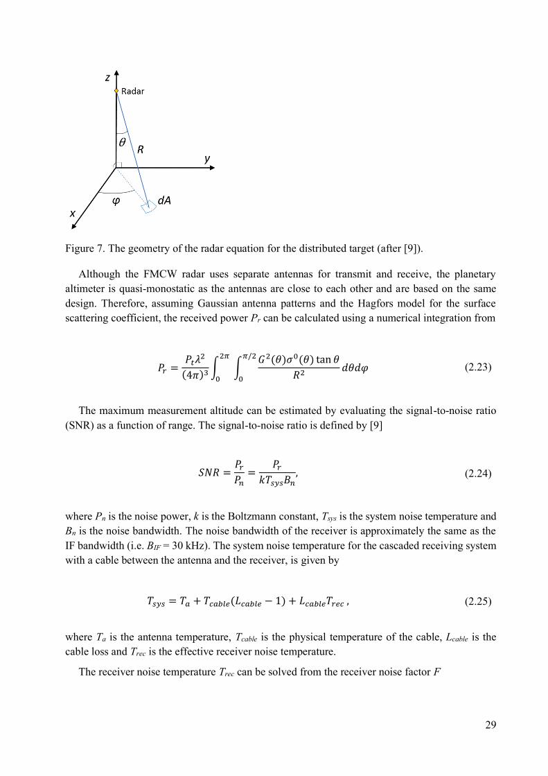
29
Figure 7. The geometry of the radar equation for the distributed target (after [9]).
Although the FMCW radar uses separate antennas for transmit and receive, the planetary
altimeter is quasi-monostatic as the antennas are close to each other and are based on the same
design. Therefore, assuming Gaussian antenna patterns and the Hagfors model for the surface
scattering coefficient, the received power Pr can be calculated using a numerical integration from
𝑃𝑟 =𝑃𝑡𝜆2
(4𝜋)3∫ ∫
𝐺2(𝜃)𝜎0(𝜃) tan 𝜃
𝑅2
𝜋/2
0
2𝜋
0
𝑑𝜃𝑑𝜑 (2.23)
The maximum measurement altitude can be estimated by evaluating the signal-to-noise ratio
(SNR) as a function of range. The signal-to-noise ratio is defined by [9]
𝑆𝑁𝑅 =𝑃𝑟
𝑃𝑛=
𝑃𝑟
𝑘𝑇𝑠𝑦𝑠𝐵𝑛, (2.24)
where Pn is the noise power, k is the Boltzmann constant, Tsys is the system noise temperature and
Bn is the noise bandwidth. The noise bandwidth of the receiver is approximately the same as the
IF bandwidth (i.e. BIF = 30 kHz). The system noise temperature for the cascaded receiving system
with a cable between the antenna and the receiver, is given by
𝑇𝑠𝑦𝑠 = 𝑇𝑎 + 𝑇𝑐𝑎𝑏𝑙𝑒(𝐿𝑐𝑎𝑏𝑙𝑒 − 1) + 𝐿𝑐𝑎𝑏𝑙𝑒𝑇𝑟𝑒𝑐 , (2.25)
where Ta is the antenna temperature, Tcable is the physical temperature of the cable, Lcable is the
cable loss and Trec is the effective receiver noise temperature.
The receiver noise temperature Trec can be solved from the receiver noise factor F
30
𝑇𝑟𝑒𝑐 = 𝑇0(𝐹 − 1) , (2.26)
where T0 is 290 K.
The antenna temperature Ta depends on the antenna pattern, frequency and antenna efficiency
in a rather complicated way. For the initial range estimates, it is often assumed that Ta = T0.
System parameters applied to predict the range of the FMCW radar altimeter are summarized
in Table 5.
Table 5. Initial system parameters to analyse the range of the FMCW radar.
Symbol Value
Transmitter
Center frequency f 13.3 GHz
Center wavelength λ 0.0225 m
Transmit power Pt 13 dBm
Antenna
Peak gain G0 24 dB
Beamwidth θ3dB 10°
Antenna temperature Ta 290 K
Antenna cable loss Lcable 0.8 dB
Cable temperature Tcable 290 K
Receiver
Noise bandwidth Bn 30 kHz
Receiver noise figure NF 6 dB (i.e. F = 3.98)
Receiver noise temperature Trec 864.5 K
System noise temperature Tsys 1388 K
Ground surface
Poorly reflective surface
εr
θrms
1.5
10°
Typical surface
εr
θrms
3.0
5°
The received power as a function of altitude was calculated by inserting Hagfors’ model
equation (2.10) and approximated Gaussian antenna pattern equation (2.21) into equation (2.23).
The surface integral in equation (2.23) was solved using a numerical integration method
(Simpson’s rule). The signal-to-noise ratio was then calculated from equation (2.24). Attenuation
due to atmospheric gases were not included in the calculations, because these are negligible on
Mars. Also, the attenuation in the case of severe dust storm was omitted. As depicted in Section
2.5, the losses in the dust storm can be L = 0.12 dB/km. At 7 km altitude, this leads to 1.7 dB
degradation of the SNR compared to the calculated values.
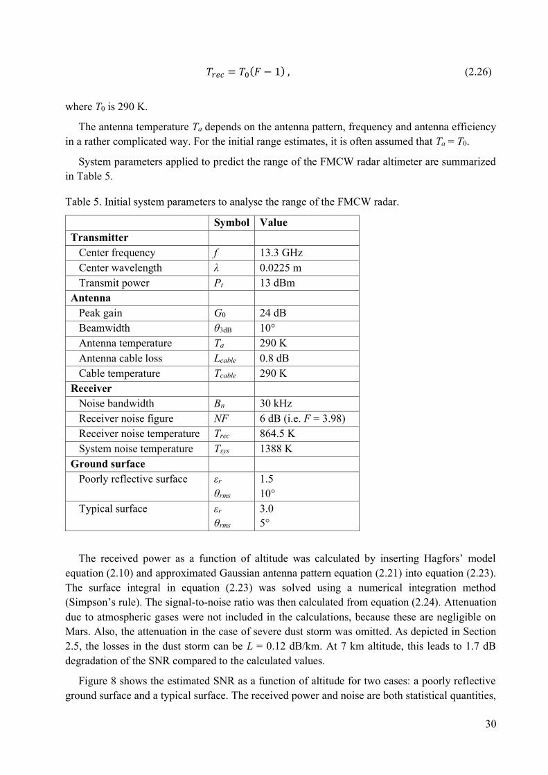
Figure 8 shows the estimated SNR as a function of altitude for two cases: a poorly reflective
ground surface and a typical surface. The received power and noise are both statistical quantities,
31
and therefore the SNR for reliable detection depends on the required probability of detection. It is
here assumed that the required SNR is higher than 10 dB. Thus, in the case of typical
backscattering conditions, the estimated maximum measurement altitude is approximately 50 km.
The maximum measurement altitude drops to approximately 11.5 km with the poorly reflective
surface. It can be concluded that there is enough reserve to fulfill the maximum altitude
requirement (7 km) with the selected system parameters. The parameters shown in Table 5 are
therefore used as target values for the design.
Figure 8. The signal-to-noise ratio (SNR) of the FMCW radar as a function of altitude, assuming
poorly reflective surface (red line: εr = 1.5, θrms = 10°) and typical surface (black line: εr = 3.0, θrms
= 5°). The green horizontal line shows the minimum SNR required for detection (SNR = 10 dB).
The dynamic input power range that the radar receiver should adapt to is a function of the
minimum and maximum measurement altitudes (10 m and 7 km, respectively). The received
power Pr was calculated at these altitudes, assuming poorly reflective and highly reflective
backscattering conditions. The calculated results are shown in Table 6. The predicted input power
range is from -30 dBm to -108 dBm. Thus, the target value for the dynamic range is 80 dB. The
gain control of the radar receiver must adapt to this large dynamic range.
Table 6. The received power Pr at the minimum and maximum measurement altitudes (with
transmit power Pt = 13 dBm and normal beam incidence).
Surface Altitude
[m]
Received power
[dBm]
Poorly reflective
(εr = 1.5, θrms = 10°)
10
7000
-51
-108
Highly reflective
(εr = 4.0, θrms = 0.5°)
10
7000
-30
-87
-10
0
10
20
30
40
50
60
70
80
90
0,01 0,1 1 10 100
SNR
[dB
]
Altitude [km]
FMCW radar range prediction
Poorly reflective
Typical surface
32
3. Design of the Ku-band FMCW radar
3.1 Functional description
In the trade-off between pulse and frequency modulated continuous wave (FMCW) radar
concepts, a servo type variant of the FMCW radar was evaluated to be the most suitable for the
planet lander. In the selected FMCW technique, the carrier is modulated using a low frequency
triangular waveform. The servo control constantly modifies the ramp rate of the modulating
waveform so that the difference frequency (or the beat frequency) fb remains constant despite the
changing distance R to the target. This method is useful when the radar has only one primary target
to measure, such as the ground surface in the planetary altimeter application. The main benefit of
the servo control is that the IF bandwidth can be made narrow, which reduces the noise in the
receiver and thus improves the signal-to-noise ratio.
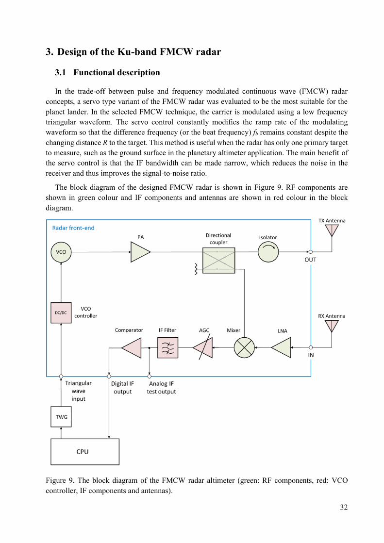
The block diagram of the designed FMCW radar is shown in Figure 9. RF components are
shown in green colour and IF components and antennas are shown in red colour in the block
diagram.
Figure 9. The block diagram of the FMCW radar altimeter (green: RF components, red: VCO
controller, IF components and antennas).
33
In this radar design, the control of the frequency modulation is performed in the radar back-end
processor (CPU) by measuring the beat frequency and adjusting the ramp rate accordingly. The
carrier signal 13.3 GHz is generated in a voltage controlled oscillator (VCO) and it is modulated
with a varying voltage at the input of the VCO. This modulating triangular wave is generated in
the radar back-end. An additional level shifter (i.e. VCO controller) is needed at the input of the
VCO to convert the voltage of the triangular wave to the correct level. The output frequency of the
VCO is directly proportional to the input control voltage and the required modulation span for the
frequency is 100 MHz (13.25 – 13.35 GHz) in this application. It is important to produce a clean,
linear ramp over the whole sweep bandwidth, because the nonlinearity of the sweep would degrade
the range resolution. The modulated signal is amplified to a desired level with a power amplifier
(PA), before it is transmitted with a planar antenna array. An isolator is placed in the front of the
antenna to suppress reflections coming back from the transmit antenna. The altimeter uses separate
antennas for transmitting (TX) and receiving (RX).
A part of the transmit signal is taken to a receiver mixer by using a directional coupler. This
signal is mixed with a returning ground echo and as a result, the beat frequency is obtained. The
beat frequency is the difference between the transmitted and received signals at a given moment.
In this servo-type radar the beat frequency is kept constant at 175 kHz by controlling the ramp rate
of the modulating triangular wave. The returning ground echo is amplified with a low noise
amplifier (LNA) before it is directed to a mixer.
The output of the receiver mixer (i.e. the beat frequency) is amplified with an active gain control
(AGC) amplifier. The altimeter is required to operate over a wide range of distances from 7 km
down to 10 m. When the returning ground echo is weak, the AGC will have high gain and when
the signal is strong at low altitudes, the AGC will have low gain. A too-high signal level would
saturate the receiver back-end and the AGC ensures that the signal is kept at the desired level.
After the AGC, the beat frequency is filtered using an IF bandpass filter with 30 kHz bandwidth.
Before sending the beat frequency to the back-end processor, the signal is converted to a square
wave with a comparator. The distance can then be calculated from the period of the modulating
triangular wave which was needed to establish the beat frequency 175 kHz.
3.2 Design of functional components
The breadboard of the radar front-end is constructed from individual RF components with
separate mechanical housings and from one electronics printed circuit board (PCB). This approach
allows each component to be tested and tuned individually during the development. Once the
performance of each individual component is satisfactory, the complete radar front-end module is
assembled from the components. In the Engineering Model phase all the RF functions can be
integrated into the same housing, which will result in significant mass and size reduction of the
radar front-end module. Integrating the RF components into the single housing will also improve
the performance, because attenuations related to cables and SMA connectors are excluded.
The housings of the RF components are manufactured from aluminum alloy with chromate
conversion coating. The dimensions of the housings depend on the size of the designed PCB for
each component. A substrate used for the RF components is Rogers RT/duroid 6002 [22]. The
dielectric constant of the substrate is εr = 2.94, the thickness of the substrate is h = 0.254 mm and
34
the copper thickness is th = 17 μm. The conductors are plated with gold. This microwave substrate
has low loss and excellent high frequency performance. The substrate is also space qualified and
qualified PCB manufacturing lines for the substrate exist in Europe. The substrate of the
electronics PCB is FR4 (εr = 4.7, h = 1.5 mm and th = 17 μm) and the PCB has 6 layers.
The RF housings are connected together using semi-rigid coaxial cables and straight-plug
adapters. Voltages are connected through the housings using feedthrough capacitors. The housings
are then attached on aluminum plates using bolts to form a rigid structure for the radar front-end
module.
The requirement for the power consumption (max. 2.5 W for the radar front-end) imposed some
compromises on the design. For example, an integrated downconverter could not be used because
of its too-high power consumption. Instead, a passive balanced mixer based on Schottky diodes
was designed. Also, a compromise had to be done regarding the output power of the radar when
designing the power amplifier and choosing the component for it.
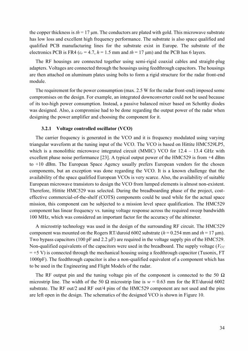
3.2.1 Voltage controlled oscillator (VCO)
The carrier frequency is generated in the VCO and it is frequency modulated using varying
triangular waveform at the tuning input of the VCO. The VCO is based on Hittite HMC529LP5,
which is a monolithic microwave integrated circuit (MMIC) VCO for 12.4 – 13.4 GHz with
excellent phase noise performance [23]. A typical output power of the HMC529 is from +4 dBm
to +10 dBm. The European Space Agency usually prefers European vendors for the chosen
components, but an exception was done regarding the VCO. It is a known challenge that the
availability of the space qualified European VCOs is very scarce. Also, the availability of suitable
European microwave transistors to design the VCO from lumped elements is almost non-existent.
Therefore, Hittite HMC529 was selected. During the breadboarding phase of the project, cost-
effective commercial-of-the-shelf (COTS) components could be used while for the actual space
mission, this component can be subjected to a mission level space qualification. The HMC529
component has linear frequency vs. tuning voltage response across the required sweep bandwidth
100 MHz, which was considered an important factor for the accuracy of the altimeter.
A microstrip technology was used in the design of the surrounding RF circuit. The HMC529
component was mounted on the Rogers RT/duroid 6002 substrate (h = 0.254 mm and th = 17 μm).
Two bypass capacitors (100 pF and 2.2 μF) are required in the voltage supply pin of the HMC529.
Non-qualified equivalents of the capacitors were used in the breadboard. The supply voltage (VCC
= +5 V) is connected through the mechanical housing using a feedthrough capacitor (Tusonix, FT
1000pF). The feedthrough capacitor is also a non-qualified equivalent of a component which has
to be used in the Engineering and Flight Models of the radar.
The RF output pin and the tuning voltage pin of the component is connected to the 50 Ω
microstrip line. The width of the 50 Ω microstrip line is w = 0.63 mm for the RT/duroid 6002
substrate. The RF out/2 and RF out/4 pins of the HMC529 component are not used and the pins
are left open in the design. The schematics of the designed VCO is shown in Figure 10.
35
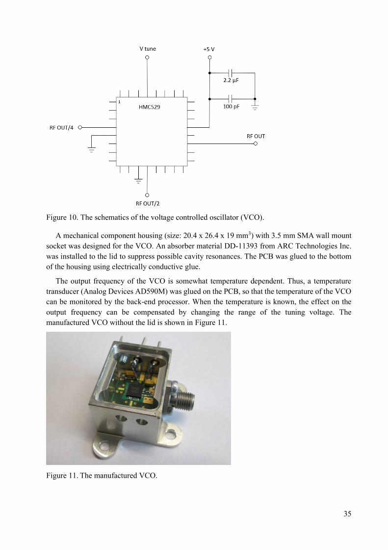
Figure 10. The schematics of the voltage controlled oscillator (VCO).
A mechanical component housing (size: 20.4 x 26.4 x 19 mm3) with 3.5 mm SMA wall mount
socket was designed for the VCO. An absorber material DD-11393 from ARC Technologies Inc.
was installed to the lid to suppress possible cavity resonances. The PCB was glued to the bottom
of the housing using electrically conductive glue.
The output frequency of the VCO is somewhat temperature dependent. Thus, a temperature
transducer (Analog Devices AD590M) was glued on the PCB, so that the temperature of the VCO
can be monitored by the back-end processor. When the temperature is known, the effect on the
output frequency can be compensated by changing the range of the tuning voltage. The
manufactured VCO without the lid is shown in Figure 11.
Figure 11. The manufactured VCO.
36
3.2.2 VCO controller
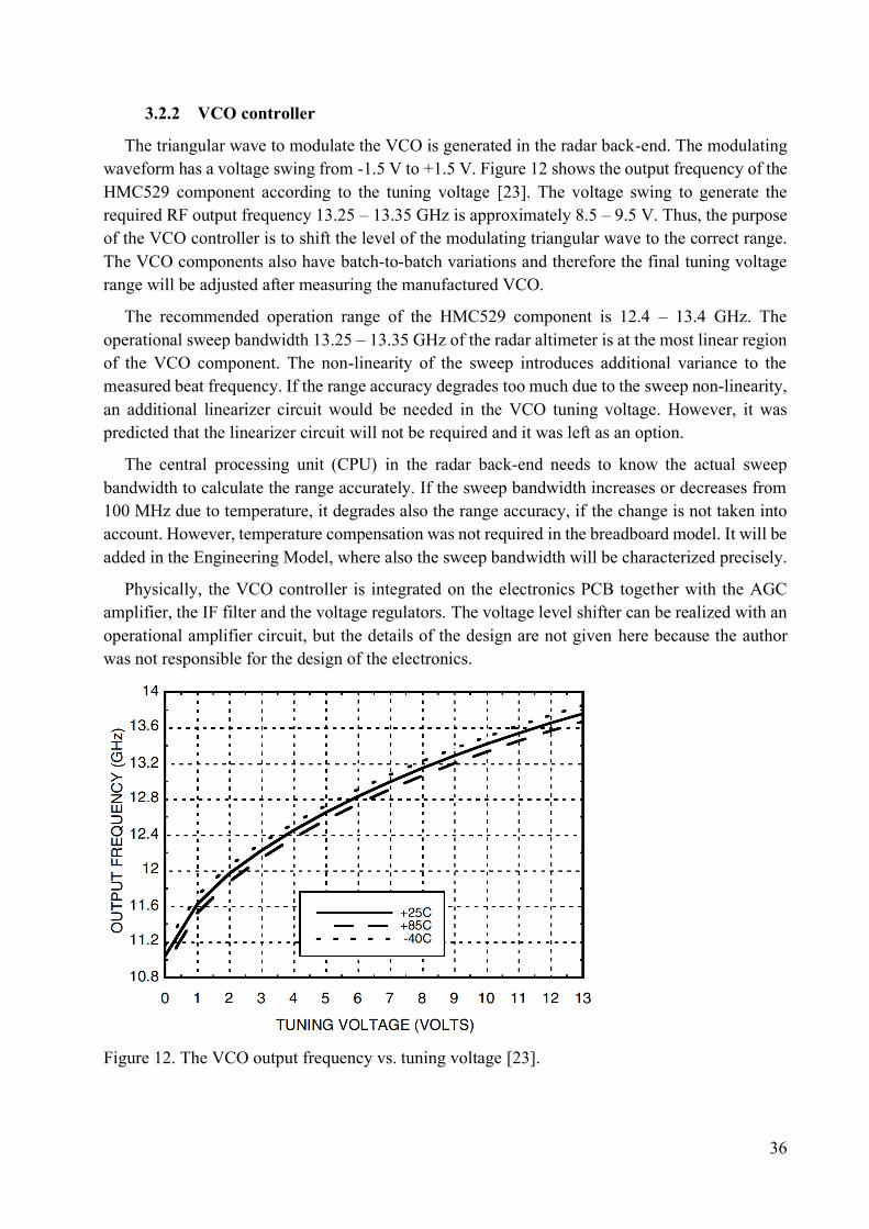
The triangular wave to modulate the VCO is generated in the radar back-end. The modulating
waveform has a voltage swing from -1.5 V to +1.5 V. Figure 12 shows the output frequency of the
HMC529 component according to the tuning voltage [23]. The voltage swing to generate the
required RF output frequency 13.25 – 13.35 GHz is approximately 8.5 – 9.5 V. Thus, the purpose
of the VCO controller is to shift the level of the modulating triangular wave to the correct range.
The VCO components also have batch-to-batch variations and therefore the final tuning voltage
range will be adjusted after measuring the manufactured VCO.
The recommended operation range of the HMC529 component is 12.4 – 13.4 GHz. The
operational sweep bandwidth 13.25 – 13.35 GHz of the radar altimeter is at the most linear region
of the VCO component. The non-linearity of the sweep introduces additional variance to the
measured beat frequency. If the range accuracy degrades too much due to the sweep non-linearity,
an additional linearizer circuit would be needed in the VCO tuning voltage. However, it was
predicted that the linearizer circuit will not be required and it was left as an option.
The central processing unit (CPU) in the radar back-end needs to know the actual sweep
bandwidth to calculate the range accurately. If the sweep bandwidth increases or decreases from
100 MHz due to temperature, it degrades also the range accuracy, if the change is not taken into
account. However, temperature compensation was not required in the breadboard model. It will be
added in the Engineering Model, where also the sweep bandwidth will be characterized precisely.
Physically, the VCO controller is integrated on the electronics PCB together with the AGC
amplifier, the IF filter and the voltage regulators. The voltage level shifter can be realized with an
operational amplifier circuit, but the details of the design are not given here because the author
was not responsible for the design of the electronics.
Figure 12. The VCO output frequency vs. tuning voltage [23].
37
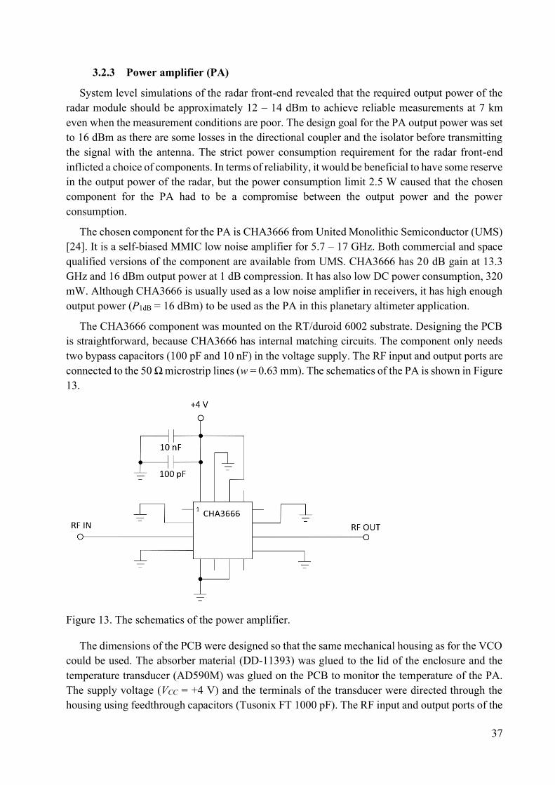
3.2.3 Power amplifier (PA)
System level simulations of the radar front-end revealed that the required output power of the
radar module should be approximately 12 – 14 dBm to achieve reliable measurements at 7 km
even when the measurement conditions are poor. The design goal for the PA output power was set
to 16 dBm as there are some losses in the directional coupler and the isolator before transmitting
the signal with the antenna. The strict power consumption requirement for the radar front-end
inflicted a choice of components. In terms of reliability, it would be beneficial to have some reserve
in the output power of the radar, but the power consumption limit 2.5 W caused that the chosen
component for the PA had to be a compromise between the output power and the power
consumption.
The chosen component for the PA is CHA3666 from United Monolithic Semiconductor (UMS)
[24]. It is a self-biased MMIC low noise amplifier for 5.7 – 17 GHz. Both commercial and space
qualified versions of the component are available from UMS. CHA3666 has 20 dB gain at 13.3
GHz and 16 dBm output power at 1 dB compression. It has also low DC power consumption, 320
mW. Although CHA3666 is usually used as a low noise amplifier in receivers, it has high enough
output power (P1dB = 16 dBm) to be used as the PA in this planetary altimeter application.
The CHA3666 component was mounted on the RT/duroid 6002 substrate. Designing the PCB
is straightforward, because CHA3666 has internal matching circuits. The component only needs
two bypass capacitors (100 pF and 10 nF) in the voltage supply. The RF input and output ports are
connected to the 50 Ω microstrip lines (w = 0.63 mm). The schematics of the PA is shown in Figure
13.
Figure 13. The schematics of the power amplifier.
The dimensions of the PCB were designed so that the same mechanical housing as for the VCO
could be used. The absorber material (DD-11393) was glued to the lid of the enclosure and the
temperature transducer (AD590M) was glued on the PCB to monitor the temperature of the PA.
The supply voltage (VCC = +4 V) and the terminals of the transducer were directed through the
housing using feedthrough capacitors (Tusonix FT 1000 pF). The RF input and output ports of the
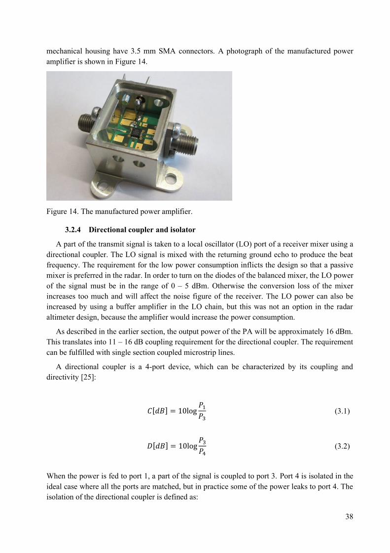
38
mechanical housing have 3.5 mm SMA connectors. A photograph of the manufactured power
amplifier is shown in Figure 14.
Figure 14. The manufactured power amplifier.
3.2.4 Directional coupler and isolator
A part of the transmit signal is taken to a local oscillator (LO) port of a receiver mixer using a
directional coupler. The LO signal is mixed with the returning ground echo to produce the beat
frequency. The requirement for the low power consumption inflicts the design so that a passive
mixer is preferred in the radar. In order to turn on the diodes of the balanced mixer, the LO power
of the signal must be in the range of 0 – 5 dBm. Otherwise the conversion loss of the mixer
increases too much and will affect the noise figure of the receiver. The LO power can also be
increased by using a buffer amplifier in the LO chain, but this was not an option in the radar
altimeter design, because the amplifier would increase the power consumption.
As described in the earlier section, the output power of the PA will be approximately 16 dBm.
This translates into 11 – 16 dB coupling requirement for the directional coupler. The requirement
can be fulfilled with single section coupled microstrip lines.
A directional coupler is a 4-port device, which can be characterized by its coupling and
directivity [25]:
𝐶[𝑑𝐵] = 10log𝑃1
𝑃3 (3.1)
𝐷[𝑑𝐵] = 10log𝑃3
𝑃4 (3.2)
When the power is fed to port 1, a part of the signal is coupled to port 3. Port 4 is isolated in the
ideal case where all the ports are matched, but in practice some of the power leaks to port 4. The
isolation of the directional coupler is defined as:
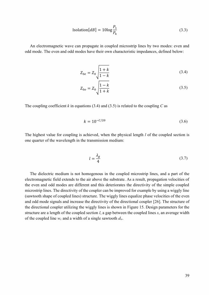
39
Isolation[𝑑𝐵] = 10log𝑃1
𝑃4 (3.3)
An electromagnetic wave can propagate in coupled microstrip lines by two modes: even and
odd mode. The even and odd modes have their own characteristic impedances, defined below:
𝑍0𝑒 = 𝑍0√1 + 𝑘
1 − 𝑘 (3.4)
𝑍0𝑜 = 𝑍0√1 − 𝑘
1 + 𝑘 (3.5)
The coupling coefficient k in equations (3.4) and (3.5) is related to the coupling C as
𝑘 = 10−𝐶/20 (3.6)
The highest value for coupling is achieved, when the physical length l of the coupled section is
one quarter of the wavelength in the transmission medium:
𝑙 =𝜆𝑔
4 (3.7)
The dielectric medium is not homogenous in the coupled microstrip lines, and a part of the
electromagnetic field extends to the air above the substrate. As a result, propagation velocities of
the even and odd modes are different and this deteriorates the directivity of the simple coupled
microstrip lines. The directivity of the coupler can be improved for example by using a wiggly line
(sawtooth shape of coupled lines) structure. The wiggly lines equalize phase velocities of the even
and odd mode signals and increase the directivity of the directional coupler [26]. The structure of
the directional coupler utilizing the wiggly lines is shown in Figure 15. Design parameters for the
structure are a length of the coupled section l, a gap between the coupled lines s, an average width
of the coupled line wc and a width of a single sawtooth dw.
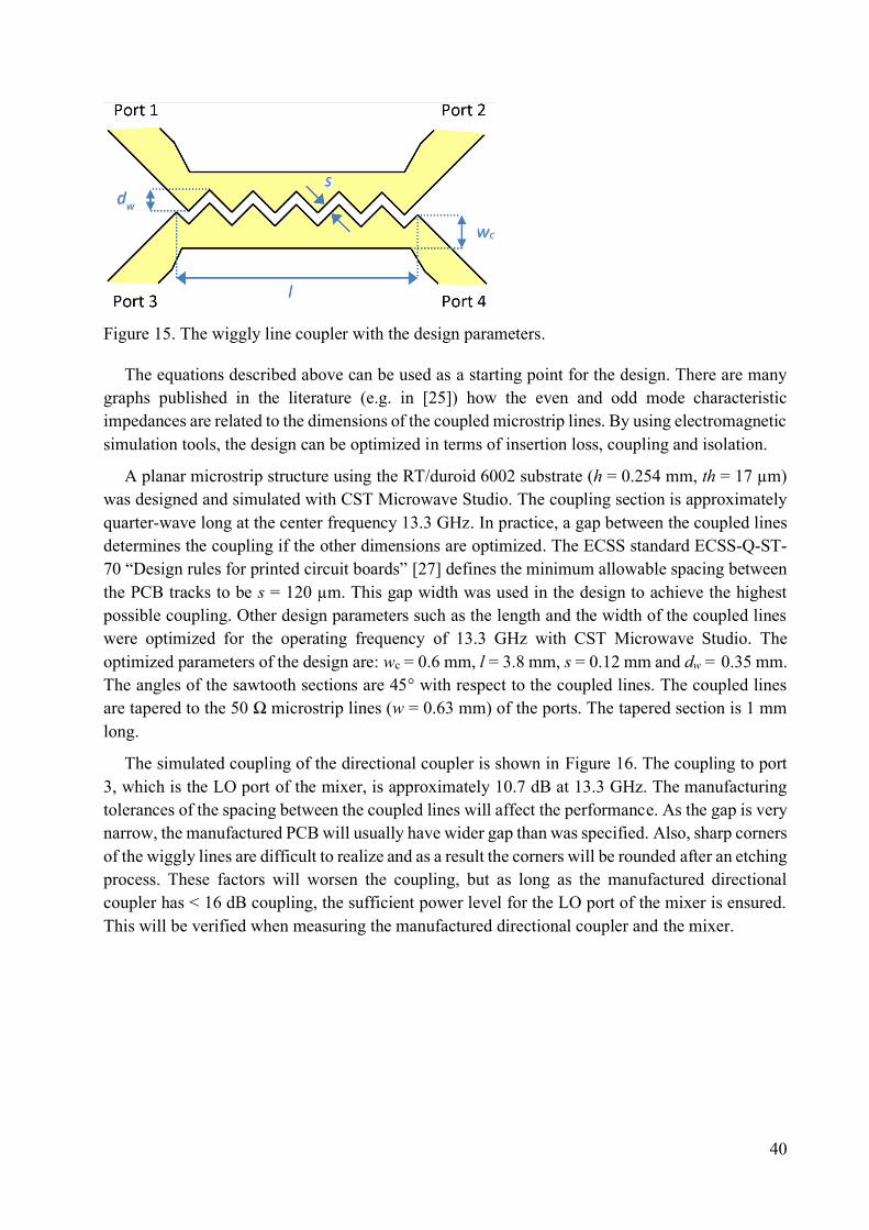
40
Figure 15. The wiggly line coupler with the design parameters.
The equations described above can be used as a starting point for the design. There are many
graphs published in the literature (e.g. in [25]) how the even and odd mode characteristic
impedances are related to the dimensions of the coupled microstrip lines. By using electromagnetic
simulation tools, the design can be optimized in terms of insertion loss, coupling and isolation.
A planar microstrip structure using the RT/duroid 6002 substrate (h = 0.254 mm, th = 17 µm)
was designed and simulated with CST Microwave Studio. The coupling section is approximately
quarter-wave long at the center frequency 13.3 GHz. In practice, a gap between the coupled lines
determines the coupling if the other dimensions are optimized. The ECSS standard ECSS-Q-ST-
70 “Design rules for printed circuit boards” [27] defines the minimum allowable spacing between
the PCB tracks to be s = 120 µm. This gap width was used in the design to achieve the highest
possible coupling. Other design parameters such as the length and the width of the coupled lines
were optimized for the operating frequency of 13.3 GHz with CST Microwave Studio. The
optimized parameters of the design are: wc = 0.6 mm, l = 3.8 mm, s = 0.12 mm and dw = 0.35 mm.
The angles of the sawtooth sections are 45° with respect to the coupled lines. The coupled lines
are tapered to the 50 Ω microstrip lines (w = 0.63 mm) of the ports. The tapered section is 1 mm
long.
The simulated coupling of the directional coupler is shown in Figure 16. The coupling to port
3, which is the LO port of the mixer, is approximately 10.7 dB at 13.3 GHz. The manufacturing
tolerances of the spacing between the coupled lines will affect the performance. As the gap is very
narrow, the manufactured PCB will usually have wider gap than was specified. Also, sharp corners
of the wiggly lines are difficult to realize and as a result the corners will be rounded after an etching
process. These factors will worsen the coupling, but as long as the manufactured directional
coupler has < 16 dB coupling, the sufficient power level for the LO port of the mixer is ensured.
This will be verified when measuring the manufactured directional coupler and the mixer.
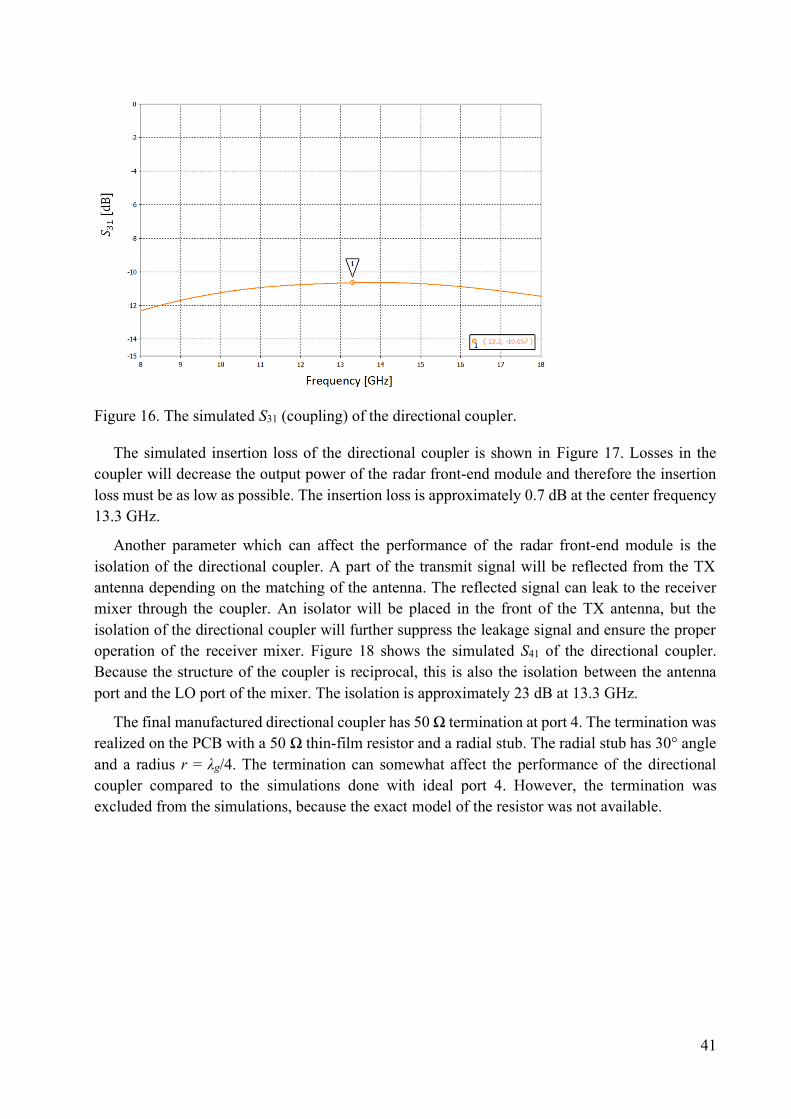
41
Figure 16. The simulated S31 (coupling) of the directional coupler.
The simulated insertion loss of the directional coupler is shown in Figure 17. Losses in the
coupler will decrease the output power of the radar front-end module and therefore the insertion
loss must be as low as possible. The insertion loss is approximately 0.7 dB at the center frequency
13.3 GHz.
Another parameter which can affect the performance of the radar front-end module is the
isolation of the directional coupler. A part of the transmit signal will be reflected from the TX
antenna depending on the matching of the antenna. The reflected signal can leak to the receiver
mixer through the coupler. An isolator will be placed in the front of the TX antenna, but the
isolation of the directional coupler will further suppress the leakage signal and ensure the proper
operation of the receiver mixer. Figure 18 shows the simulated S41 of the directional coupler.
Because the structure of the coupler is reciprocal, this is also the isolation between the antenna
port and the LO port of the mixer. The isolation is approximately 23 dB at 13.3 GHz.
The final manufactured directional coupler has 50 Ω termination at port 4. The termination was
realized on the PCB with a 50 Ω thin-film resistor and a radial stub. The radial stub has 30° angle
and a radius r = λg/4. The termination can somewhat affect the performance of the directional
coupler compared to the simulations done with ideal port 4. However, the termination was
excluded from the simulations, because the exact model of the resistor was not available.
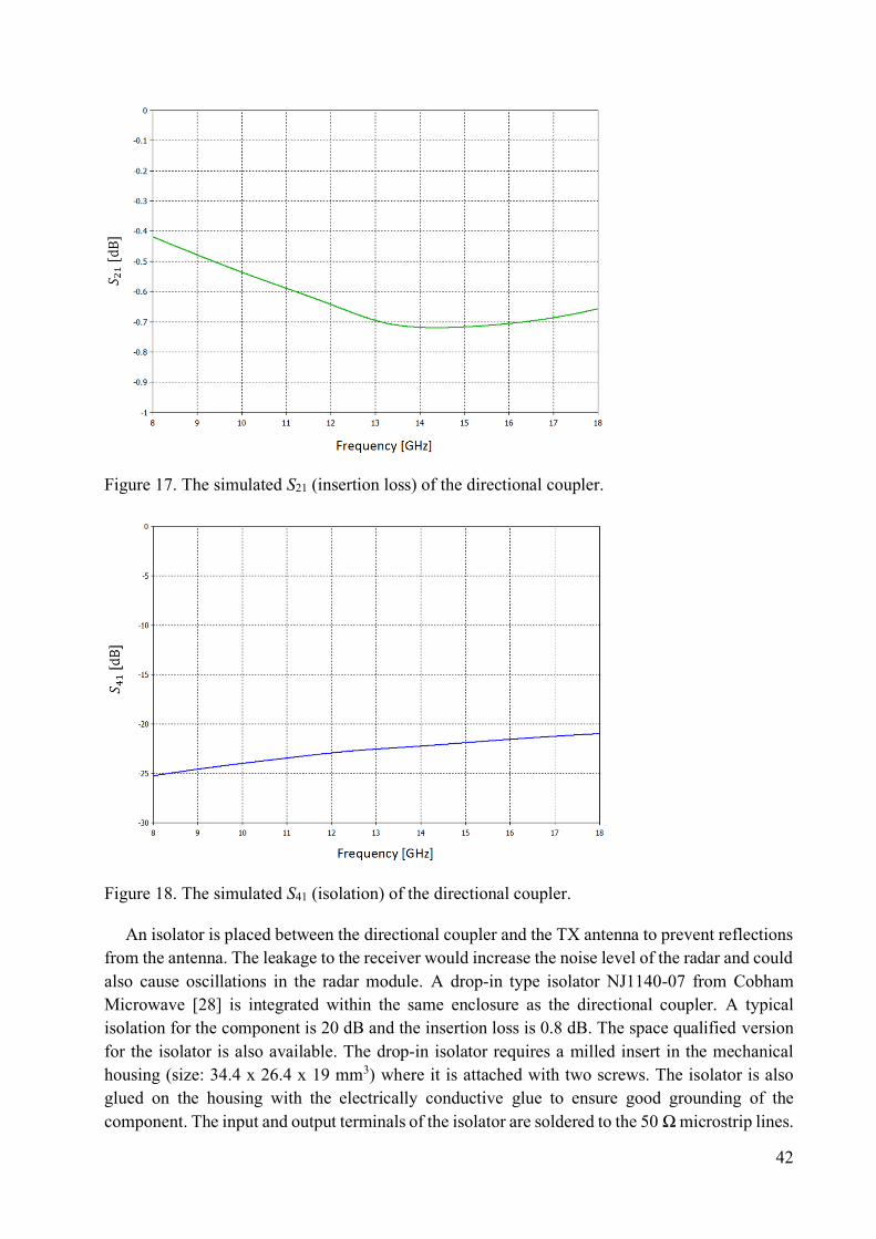
42
Figure 17. The simulated S21 (insertion loss) of the directional coupler.
Figure 18. The simulated S41 (isolation) of the directional coupler.
An isolator is placed between the directional coupler and the TX antenna to prevent reflections
from the antenna. The leakage to the receiver would increase the noise level of the radar and could
also cause oscillations in the radar module. A drop-in type isolator NJ1140-07 from Cobham
Microwave [28] is integrated within the same enclosure as the directional coupler. A typical
isolation for the component is 20 dB and the insertion loss is 0.8 dB. The space qualified version
for the isolator is also available. The drop-in isolator requires a milled insert in the mechanical
housing (size: 34.4 x 26.4 x 19 mm3) where it is attached with two screws. The isolator is also
glued on the housing with the electrically conductive glue to ensure good grounding of the
component. The input and output terminals of the isolator are soldered to the 50 Ω microstrip lines.
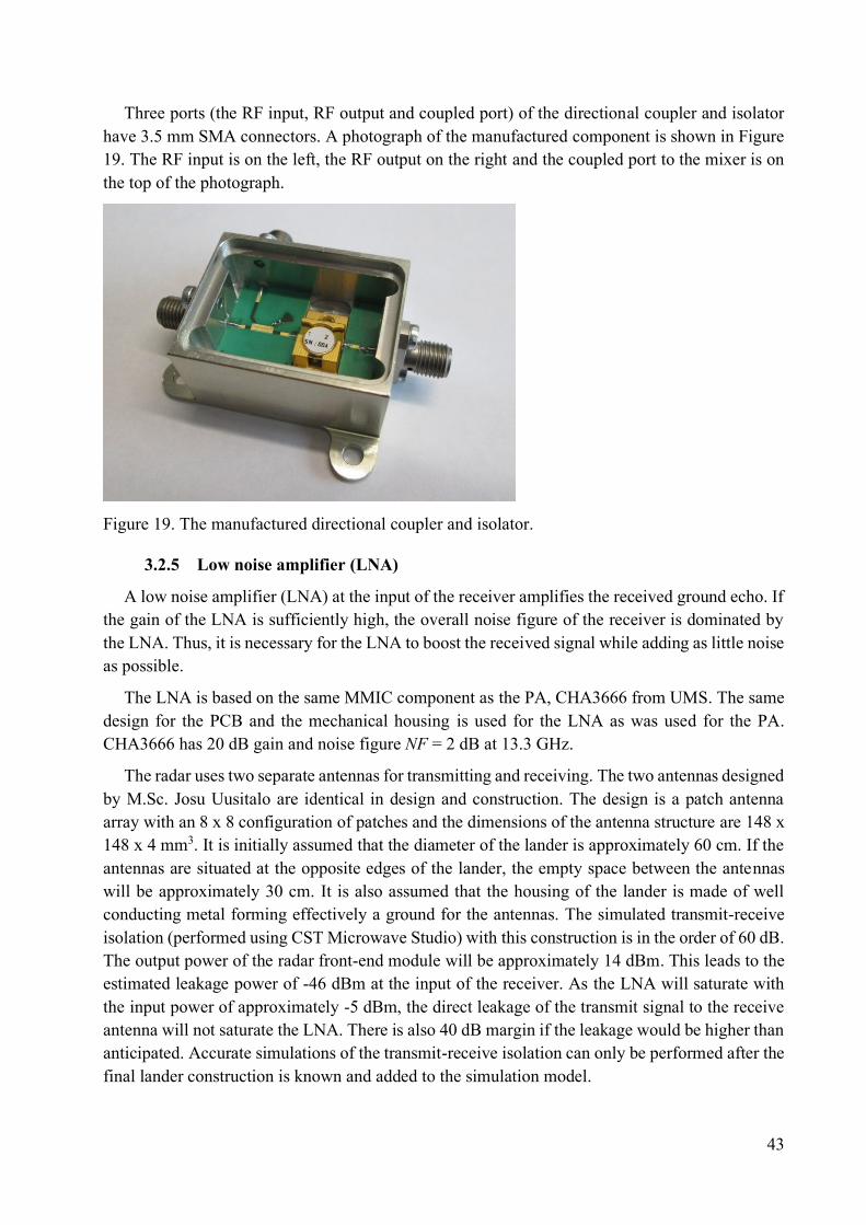
43
Three ports (the RF input, RF output and coupled port) of the directional coupler and isolator
have 3.5 mm SMA connectors. A photograph of the manufactured component is shown in Figure
19. The RF input is on the left, the RF output on the right and the coupled port to the mixer is on
the top of the photograph.
Figure 19. The manufactured directional coupler and isolator.
3.2.5 Low noise amplifier (LNA)
A low noise amplifier (LNA) at the input of the receiver amplifies the received ground echo. If
the gain of the LNA is sufficiently high, the overall noise figure of the receiver is dominated by
the LNA. Thus, it is necessary for the LNA to boost the received signal while adding as little noise
as possible.
The LNA is based on the same MMIC component as the PA, CHA3666 from UMS. The same
design for the PCB and the mechanical housing is used for the LNA as was used for the PA.
CHA3666 has 20 dB gain and noise figure NF = 2 dB at 13.3 GHz.
The radar uses two separate antennas for transmitting and receiving. The two antennas designed
by M.Sc. Josu Uusitalo are identical in design and construction. The design is a patch antenna
array with an 8 x 8 configuration of patches and the dimensions of the antenna structure are 148 x
148 x 4 mm3. It is initially assumed that the diameter of the lander is approximately 60 cm. If the
antennas are situated at the opposite edges of the lander, the empty space between the antennas
will be approximately 30 cm. It is also assumed that the housing of the lander is made of well
conducting metal forming effectively a ground for the antennas. The simulated transmit-receive
isolation (performed using CST Microwave Studio) with this construction is in the order of 60 dB.
The output power of the radar front-end module will be approximately 14 dBm. This leads to the
estimated leakage power of -46 dBm at the input of the receiver. As the LNA will saturate with
the input power of approximately -5 dBm, the direct leakage of the transmit signal to the receive
antenna will not saturate the LNA. There is also 40 dB margin if the leakage would be higher than
anticipated. Accurate simulations of the transmit-receive isolation can only be performed after the
final lander construction is known and added to the simulation model.
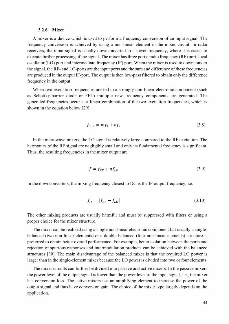
44
3.2.6 Mixer
A mixer is a device which is used to perform a frequency conversion of an input signal. The
frequency conversion is achieved by using a non-linear element in the mixer circuit. In radar
receivers, the input signal is usually downconverted to a lower frequency, where it is easier to
execute further processing of the signal. The mixer has three ports: radio frequency (RF) port, local
oscillator (LO) port and intermediate frequency (IF) port. When the mixer is used to downconvert
the signal, the RF- and LO-ports are the input ports and the sum and difference of these frequencies
are produced in the output IF-port. The output is then low-pass filtered to obtain only the difference
frequency in the output.
When two excitation frequencies are fed to a strongly non-linear electronic component (such
as Schottky-barrier diode or FET) multiple new frequency components are generated. The
generated frequencies occur at a linear combination of the two excitation frequencies, which is
shown in the equation below [29]:
𝑓𝑚,𝑛 = 𝑚𝑓1 + 𝑛𝑓2 (3.8)
In the microwave mixers, the LO signal is relatively large compared to the RF excitation. The
harmonics of the RF signal are negligibly small and only its fundamental frequency is significant.
Thus, the resulting frequencies in the mixer output are
𝑓 = 𝑓𝑅𝐹 + 𝑛𝑓𝐿𝑂 (3.9)
In the downconverters, the mixing frequency closest to DC is the IF output frequency, i.e.
𝑓𝐼𝐹 = |𝑓𝑅𝐹 − 𝑓𝐿𝑂| (3.10)
The other mixing products are usually harmful and must be suppressed with filters or using a
proper choice for the mixer structure.
The mixer can be realized using a single non-linear electronic component but usually a single-
balanced (two non-linear elements) or a double-balanced (four non-linear elements) structure is
preferred to obtain better overall performance. For example, better isolation between the ports and
rejection of spurious responses and intermodulation products can be achieved with the balanced
structures [30]. The main disadvantage of the balanced mixer is that the required LO power is
larger than in the single-element mixer because the LO power is divided into two or four elements.
The mixer circuits can further be divided into passive and active mixers. In the passive mixers
the power level of the output signal is lower than the power level of the input signal, i.e., the mixer
has conversion loss. The active mixers use an amplifying element to increase the power of the
output signal and thus have conversion gain. The choice of the mixer type largely depends on the
application.
45
In the FMCW radar, the frequency of the received ground echo differs from the transmitted
signal. The ground echo is directed to the RF-port of the mixer and a part of the transmit signal is
directed to the LO-port. The difference frequency is obtained in the IF-port. In the servo-type
FMCW radar where the period of the modulating signal is constantly adjusted, the difference
frequency is also called the beat frequency. In this planetary altimeter application, the passive
single-balanced structure was chosen for the mixer mainly because of tight power consumption
requirements. In the single-balanced mixer, two diodes are connected by using a 90° or 180°
hybrid.
The 180° hybrids are more common in the microwave applications, because they have some
benefits over the 90° hybrids. The 180° hybrids have usually larger bandwidth, better spurious and
intermodulation rejection and the RF and LO ports are easier to match [31]. A popular design when
utilizing the microstrip technology is a ring or rat-race hybrid, which is shown in Figure 20. All
four ports of the ring hybrid have a characteristic impedance Z0 (in most cases 50 Ω). The
characteristic impedance of the ring is Z0√2. The spacing between ports 2 and 4 is 3λg/4 and the
spacings between all other adjacent ports are λg/4. When the power is applied to any of the ports,
it is equally divided between the two adjacent ports. The remaining port is isolated, because the
longer signal path introduces a phase reversal and the signals are effectively cancelled. For
example, if the RF signal is applied to port 1, it is equally divided between ports 2 and 3. Port 4 is
isolated from port 1 and it is therefore selected as the LO port. The LO signal applied to port 4 is
also equally divided between ports 2 and 3, but the signals at these ports have 180° phase
difference. This property makes the ring hybrid useful in the balanced mixers as the mixer diodes
can now be connected to ports 2 and 3.
Figure 20. The 180° rat-race hybrid (after [29]).
The passive single-balanced mixer requires a certain power level for the LO signal to turn on
the diodes of the mixer. According to the simulations of the directional coupler, tight enough
coupling can be achieved for the LO drive of the balanced mixer without a need for a buffer
amplifier. However, the balanced mixer has two input responses at frequencies above and below
the LO-frequency. Since only one of the side bands contains the signal (the other side band is
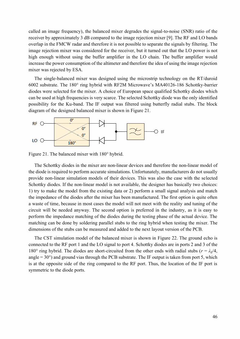
46
called an image frequency), the balanced mixer degrades the signal-to-noise (SNR) ratio of the
receiver by approximately 3 dB compared to the image rejection mixer [9]. The RF and LO bands
overlap in the FMCW radar and therefore it is not possible to separate the signals by filtering. The
image rejection mixer was considered for the receiver, but it turned out that the LO power is not
high enough without using the buffer amplifier in the LO chain. The buffer amplifier would
increase the power consumption of the altimeter and therefore the idea of using the image rejection
mixer was rejected by ESA.
The single-balanced mixer was designed using the microstrip technology on the RT/duroid
6002 substrate. The 180° ring hybrid with RF2M Microwave’s MA40126-186 Schottky-barrier
diodes were selected for the mixer. A choice of European space qualified Schottky diodes which
can be used at high frequencies is very scarce. The selected Schottky diode was the only identified
possibility for the Ku-band. The IF output was filtered using butterfly radial stubs. The block
diagram of the designed balanced mixer is shown in Figure 21.
Figure 21. The balanced mixer with 180° hybrid.
The Schottky diodes in the mixer are non-linear devices and therefore the non-linear model of
the diode is required to perform accurate simulations. Unfortunately, manufacturers do not usually
provide non-linear simulation models of their devices. This was also the case with the selected
Schottky diodes. If the non-linear model is not available, the designer has basically two choices:
1) try to make the model from the existing data or 2) perform a small signal analysis and match
the impedance of the diodes after the mixer has been manufactured. The first option is quite often
a waste of time, because in most cases the model will not meet with the reality and tuning of the
circuit will be needed anyway. The second option is preferred in the industry, as it is easy to
perform the impedance matching of the diodes during the testing phase of the actual device. The
matching can be done by soldering parallel stubs to the ring hybrid when testing the mixer. The
dimensions of the stubs can be measured and added to the next layout version of the PCB.
The CST simulation model of the balanced mixer is shown in Figure 22. The ground echo is
connected to the RF port 1 and the LO signal to port 4. Schottky diodes are in ports 2 and 3 of the
180° ring hybrid. The diodes are short-circuited from the other ends with radial stubs (r = λg/4,
angle = 30°) and ground vias through the PCB substrate. The IF output is taken from port 5, which
is at the opposite side of the ring compared to the RF port. Thus, the location of the IF port is
symmetric to the diode ports.
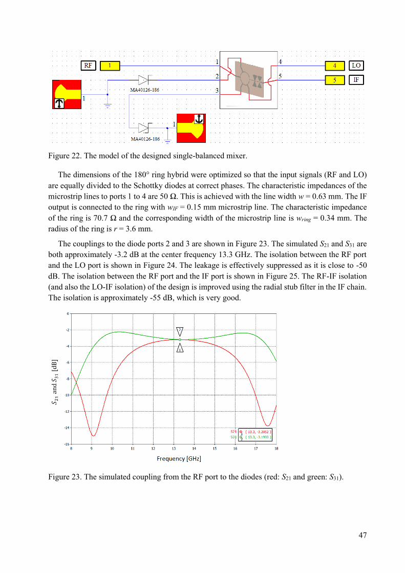
47
Figure 22. The model of the designed single-balanced mixer.
The dimensions of the 180° ring hybrid were optimized so that the input signals (RF and LO)
are equally divided to the Schottky diodes at correct phases. The characteristic impedances of the
microstrip lines to ports 1 to 4 are 50 Ω. This is achieved with the line width w = 0.63 mm. The IF
output is connected to the ring with wIF = 0.15 mm microstrip line. The characteristic impedance
of the ring is 70.7 Ω and the corresponding width of the microstrip line is wring = 0.34 mm. The
radius of the ring is r = 3.6 mm.
The couplings to the diode ports 2 and 3 are shown in Figure 23. The simulated S21 and S31 are
both approximately -3.2 dB at the center frequency 13.3 GHz. The isolation between the RF port
and the LO port is shown in Figure 24. The leakage is effectively suppressed as it is close to -50
dB. The isolation between the RF port and the IF port is shown in Figure 25. The RF-IF isolation
(and also the LO-IF isolation) of the design is improved using the radial stub filter in the IF chain.
The isolation is approximately -55 dB, which is very good.
Figure 23. The simulated coupling from the RF port to the diodes (red: S21 and green: S31).
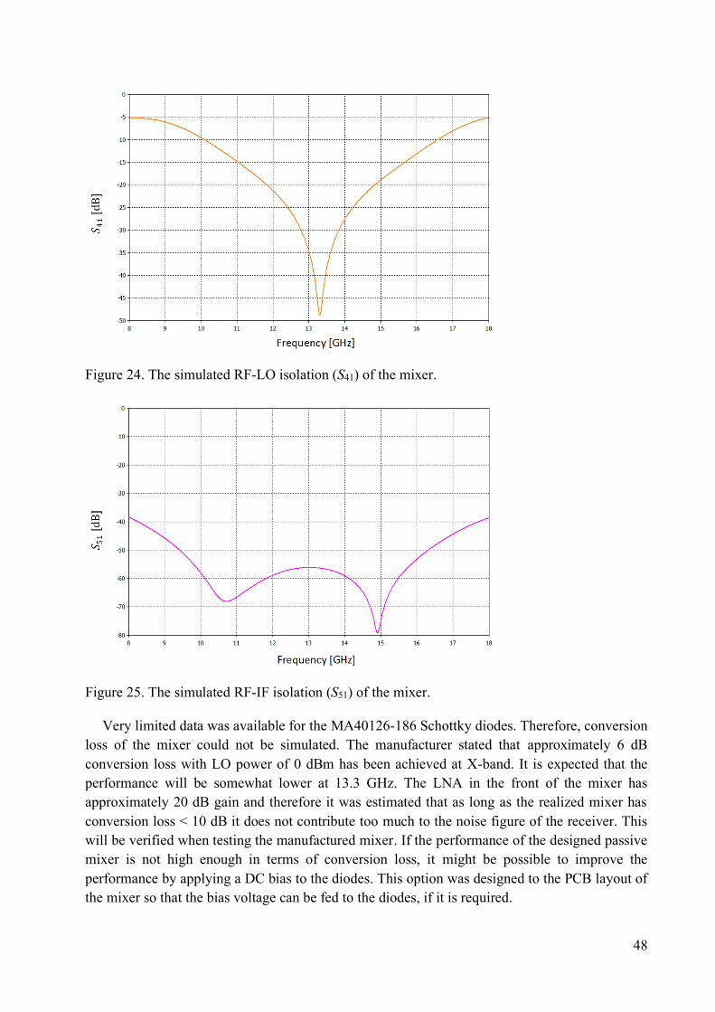
48
Figure 24. The simulated RF-LO isolation (S41) of the mixer.
Figure 25. The simulated RF-IF isolation (S51) of the mixer.
Very limited data was available for the MA40126-186 Schottky diodes. Therefore, conversion
loss of the mixer could not be simulated. The manufacturer stated that approximately 6 dB
conversion loss with LO power of 0 dBm has been achieved at X-band. It is expected that the
performance will be somewhat lower at 13.3 GHz. The LNA in the front of the mixer has
approximately 20 dB gain and therefore it was estimated that as long as the realized mixer has
conversion loss < 10 dB it does not contribute too much to the noise figure of the receiver. This
will be verified when testing the manufactured mixer. If the performance of the designed passive
mixer is not high enough in terms of conversion loss, it might be possible to improve the
performance by applying a DC bias to the diodes. This option was designed to the PCB layout of
the mixer so that the bias voltage can be fed to the diodes, if it is required.
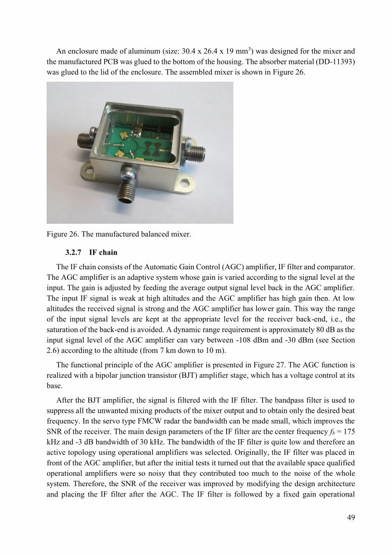
49
An enclosure made of aluminum (size: 30.4 x 26.4 x 19 mm3) was designed for the mixer and
the manufactured PCB was glued to the bottom of the housing. The absorber material (DD-11393)
was glued to the lid of the enclosure. The assembled mixer is shown in Figure 26.
Figure 26. The manufactured balanced mixer.
3.2.7 IF chain
The IF chain consists of the Automatic Gain Control (AGC) amplifier, IF filter and comparator.
The AGC amplifier is an adaptive system whose gain is varied according to the signal level at the
input. The gain is adjusted by feeding the average output signal level back in the AGC amplifier.
The input IF signal is weak at high altitudes and the AGC amplifier has high gain then. At low
altitudes the received signal is strong and the AGC amplifier has lower gain. This way the range
of the input signal levels are kept at the appropriate level for the receiver back-end, i.e., the
saturation of the back-end is avoided. A dynamic range requirement is approximately 80 dB as the
input signal level of the AGC amplifier can vary between -108 dBm and -30 dBm (see Section
2.6) according to the altitude (from 7 km down to 10 m).
The functional principle of the AGC amplifier is presented in Figure 27. The AGC function is
realized with a bipolar junction transistor (BJT) amplifier stage, which has a voltage control at its
base.
After the BJT amplifier, the signal is filtered with the IF filter. The bandpass filter is used to
suppress all the unwanted mixing products of the mixer output and to obtain only the desired beat
frequency. In the servo type FMCW radar the bandwidth can be made small, which improves the
SNR of the receiver. The main design parameters of the IF filter are the center frequency fb = 175
kHz and -3 dB bandwidth of 30 kHz. The bandwidth of the IF filter is quite low and therefore an
active topology using operational amplifiers was selected. Originally, the IF filter was placed in
front of the AGC amplifier, but after the initial tests it turned out that the available space qualified
operational amplifiers were so noisy that they contributed too much to the noise of the whole
system. Therefore, the SNR of the receiver was improved by modifying the design architecture
and placing the IF filter after the AGC. The IF filter is followed by a fixed gain operational
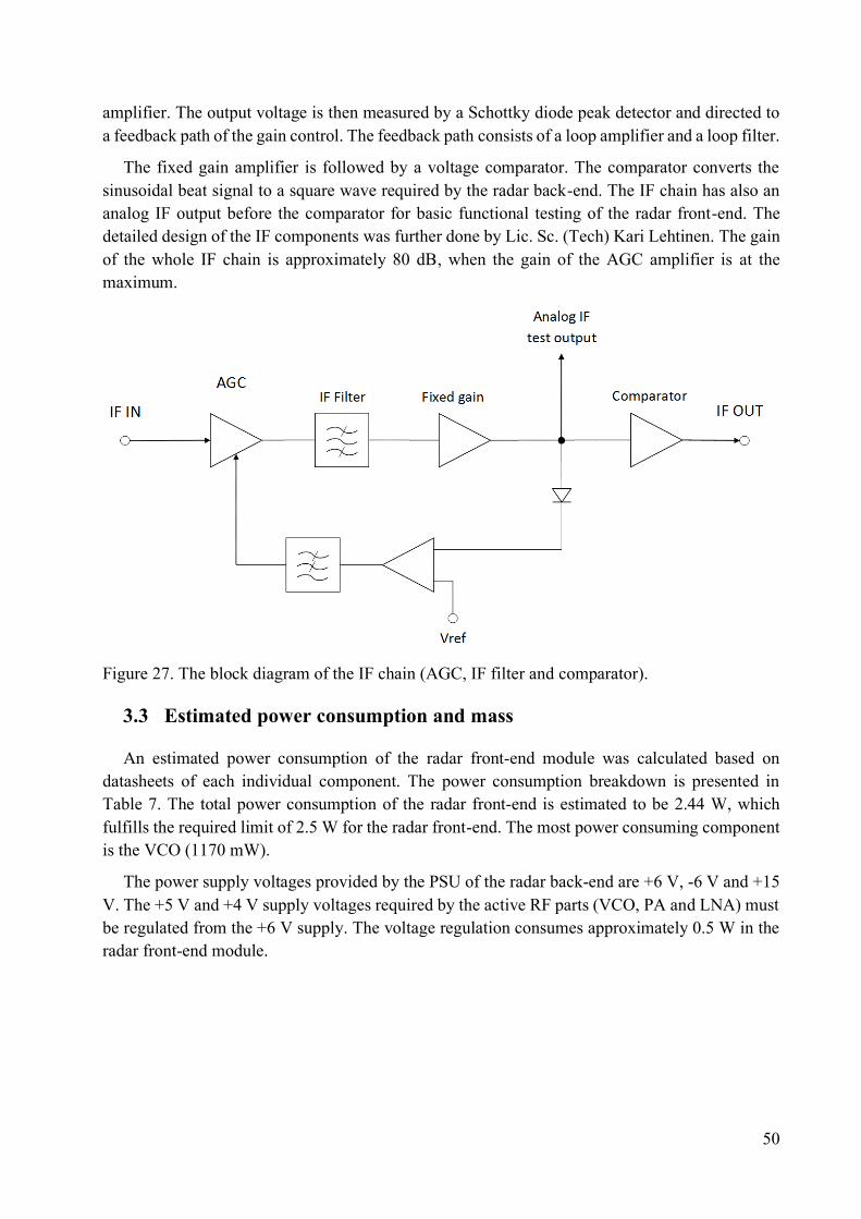
50
amplifier. The output voltage is then measured by a Schottky diode peak detector and directed to
a feedback path of the gain control. The feedback path consists of a loop amplifier and a loop filter.
The fixed gain amplifier is followed by a voltage comparator. The comparator converts the
sinusoidal beat signal to a square wave required by the radar back-end. The IF chain has also an
analog IF output before the comparator for basic functional testing of the radar front-end. The
detailed design of the IF components was further done by Lic. Sc. (Tech) Kari Lehtinen. The gain
of the whole IF chain is approximately 80 dB, when the gain of the AGC amplifier is at the
maximum.
Figure 27. The block diagram of the IF chain (AGC, IF filter and comparator).
3.3 Estimated power consumption and mass
An estimated power consumption of the radar front-end module was calculated based on
datasheets of each individual component. The power consumption breakdown is presented in
Table 7. The total power consumption of the radar front-end is estimated to be 2.44 W, which
fulfills the required limit of 2.5 W for the radar front-end. The most power consuming component
is the VCO (1170 mW).
The power supply voltages provided by the PSU of the radar back-end are +6 V, -6 V and +15
V. The +5 V and +4 V supply voltages required by the active RF parts (VCO, PA and LNA) must
be regulated from the +6 V supply. The voltage regulation consumes approximately 0.5 W in the
radar front-end module.
51
Table 7. The estimated power consumption of the TX/RX module.
Component Power consumption P [mW]
Component Regulation Total
VCO (VCC=+5V) 975 195 1170
PA (VCC=+4V) 320 160 480
LNA (VCC=+4V) 320 160 480
AGC (VCC=+6V) 200 0 200
IF filter (VCC=+6V) 50 0 50
VCO controller (VCC=+12V) 60 0 60
Total power consumption 1925 515 2440
An estimated mass was calculated based on the selected parts and the dimensions of the
individual component housings. The mass breakdown is shown in Table 8. The estimated mass of
the breadboard module is approximately 0.5 kg, which is less than the maximum target mass 0.67
kg.
Table 8. The estimated mass of the TX/RX module.
Component Mass [g]
VCO 26
PA 29
Directional coupler 51
LNA 29
Mixer 39
EEE parts 20
Electronics PCB 69
Mounting decks 151
D-Sub HD44 connector 13
RF cable harness 75
Wires 10
Total mass 512
3.4 Breadboard of the radar front-end
The developed RF components were attached on two aluminum plates (size: 146 x 96 x 2 mm3).
One plate was used for the transmitter parts (the VCO, PA and directional coupler) and another
plate for the receiver parts (the LNA and mixer). The third deck of the radar front-end module is
formed by the electronics PCB.
RF interconnections between the individual RF components were done with straight SMA
adapters and coaxial cables (Huber+Suhner Suco-Form). The tuning voltage of the VCO is
sensitive to an external radio frequency interference (RFI). Therefore, a coaxial cable was used to
connect the tuning voltage to the electronics PCB. RF interfaces to the transmitting (TX) and
receiving (RX) antennas are 3.5 mm SMA wall mount sockets (ESCC 3402/002 variant 18 from
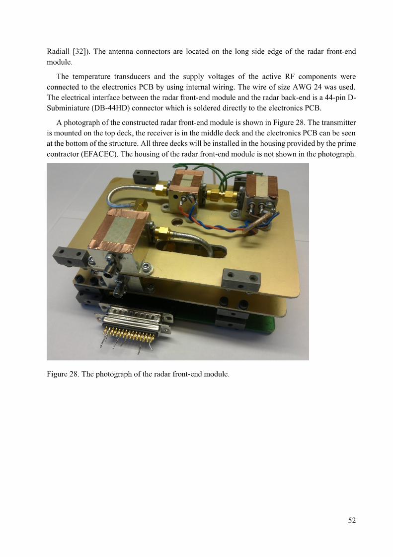
52
Radiall [32]). The antenna connectors are located on the long side edge of the radar front-end
module.
The temperature transducers and the supply voltages of the active RF components were
connected to the electronics PCB by using internal wiring. The wire of size AWG 24 was used.
The electrical interface between the radar front-end module and the radar back-end is a 44-pin D-
Subminiature (DB-44HD) connector which is soldered directly to the electronics PCB.
A photograph of the constructed radar front-end module is shown in Figure 28. The transmitter
is mounted on the top deck, the receiver is in the middle deck and the electronics PCB can be seen
at the bottom of the structure. All three decks will be installed in the housing provided by the prime
contractor (EFACEC). The housing of the radar front-end module is not shown in the photograph.
Figure 28. The photograph of the radar front-end module.
53
4. Measurements of functional components
4.1 VCO measurements
Three VCO units were manufactured and their performance was verified with measurements.
Tuning voltage and power supply inputs of the VCO were connected to a laboratory bench power
supply in initial tests. The output frequency was measured with a spectrum analyzer.
It was discovered early on that the tuning voltage of the VCO is sensitive to an external radio
frequency interference (RFI). During certain office hours the phase noise of the output signal
increased significantly and occasionally the signal had additional spikes. A testing laboratory of
Harp Technologies is situated in a crowded office building, where there are multiple wireless RFI
sources from various commercial companies. Early mornings and late evenings were identified as
quiet hours for testing, but the actual source of RFI was never discovered. A measurement set-up
was also improved by using coaxial cables in the inputs of the VCO and a special care was taken
to minimize ground loops. However, these measures were not enough to completely remove the
sensitivity to RFI from two of the manufactured VCO units. The VCO units were then tested
outside the facilities of Harp in quiet RF environment, where the problem disappeared completely.
Although one VCO unit was less sensitive to RFI and was deemed good enough for the
breadboard, a design change was decided for the following Engineering Model phase of the
project. In the breadboard model, the triangular wave generator is located at the radar back-end.
The triangular wave generator will be brought to the radar front-end in the Engineering Model,
where all the radar front-end parts will be integrated into the same housing. Also, the VCO
controller circuitry will be placed as close as possible to the VCO and proper grounding is ensured
in the electronics PCB layout. It is expected that these measures will improve the performance of
the VCO.
A behavior of the best VCO unit was characterized in a thermal chamber. The required
frequency bandwidth of the radar is 13.25 – 13.35 GHz. At first, five different VCO control voltage
values to achieve the required frequency range were measured at room temperature T = +20°C.
The measured voltages are shown in Table 9. The frequency bandwidth is obtained with the control
voltage values ranging from 11.79 V to 12.74 V. The values are higher than anticipated from the
datasheet of the HMC529 component (see 3.2.2, Figure 12), because the expected values were in
the range of 8.5 to 9.5 V. However, according to the manufacturer (Hittite), the performance is in
the range of production tolerances. As a consequence, the variation of the tuning voltage must be
taken into account in the VCO controller circuit for the Engineering Model. The design cannot be
locked based on the measurements performed for the VCO used in the breadboard model.
Table 9. The measured VCO tuning voltages at room temperature.
Frequency Voltage
13.25 GHz 11.79 V
13.275 GHz 12.02 V
13.3 GHz 12.26 V
13.325 GHz 12.5 V
13.35 GHz 12.74 V
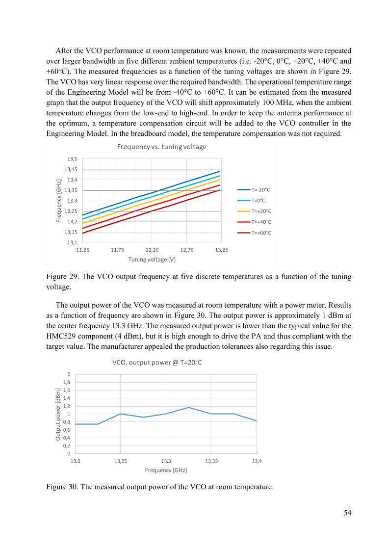
54
After the VCO performance at room temperature was known, the measurements were repeated
over larger bandwidth in five different ambient temperatures (i.e. -20°C, 0°C, +20°C, +40°C and
+60°C). The measured frequencies as a function of the tuning voltages are shown in Figure 29.
The VCO has very linear response over the required bandwidth. The operational temperature range
of the Engineering Model will be from -40°C to +60°C. It can be estimated from the measured
graph that the output frequency of the VCO will shift approximately 100 MHz, when the ambient
temperature changes from the low-end to high-end. In order to keep the antenna performance at
the optimum, a temperature compensation circuit will be added to the VCO controller in the
Engineering Model. In the breadboard model, the temperature compensation was not required.
Figure 29. The VCO output frequency at five discrete temperatures as a function of the tuning
voltage.
The output power of the VCO was measured at room temperature with a power meter. Results
as a function of frequency are shown in Figure 30. The output power is approximately 1 dBm at
the center frequency 13.3 GHz. The measured output power is lower than the typical value for the
HMC529 component (4 dBm), but it is high enough to drive the PA and thus compliant with the
target value. The manufacturer appealed the production tolerances also regarding this issue.
Figure 30. The measured output power of the VCO at room temperature.
13,1
13,15
13,2
13,25
13,3
13,35
13,4
13,45
13,5
11,25 11,75 12,25 12,75 13,25
Freq
uen
cy [G
Hz]
Tuning voltage [V]
Frequency vs. tuning voltage
T=-20°C
T=0°C
T=+20°C
T=+40°C
T=+60°C
0
0,2
0,4
0,6
0,8
1
1,2
1,4
1,6
1,8
2
13,2 13,25 13,3 13,35 13,4
Ou
tpu
t p
ow
er [d
Bm
]
Frequency [GHz]
VCO, output power @ T=20°C
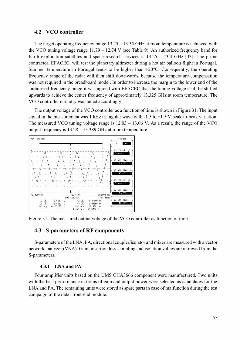
55
4.2 VCO controller
The target operating frequency range 13.25 – 13.35 GHz at room temperature is achieved with
the VCO tuning voltage range 11.79 – 12.74 V (see Table 9). An authorized frequency band for
Earth exploration satellites and space research services is 13.25 – 13.4 GHz [33]. The prime
contractor, EFACEC, will test the planetary altimeter during a hot air balloon flight in Portugal.
Summer temperature in Portugal tends to be higher than +20°C. Consequently, the operating
frequency range of the radar will then shift downwards, because the temperature compensation
was not required in the breadboard model. In order to increase the margin to the lower end of the
authorized frequency range it was agreed with EFACEC that the tuning voltage shall be shifted
upwards to achieve the center frequency of approximately 13.325 GHz at room temperature. The
VCO controller circuitry was tuned accordingly.
The output voltage of the VCO controller as a function of time is shown in Figure 31. The input
signal in the measurement was 1 kHz triangular wave with -1.5 to +1.5 V peak-to-peak variation.
The measured VCO tuning voltage range is 12.03 – 13.06 V. As a result, the range of the VCO
output frequency is 13.28 – 13.389 GHz at room temperature.
Figure 31. The measured output voltage of the VCO controller as function of time.
4.3 S-parameters of RF components
S-parameters of the LNA, PA, directional coupler/isolator and mixer are measured with a vector
network analyzer (VNA). Gain, insertion loss, coupling and isolation values are retrieved from the
S-parameters.
4.3.1 LNA and PA
Four amplifier units based on the UMS CHA3666 component were manufactured. Two units
with the best performance in terms of gain and output power were selected as candidates for the
LNA and PA. The remaining units were stored as spare parts in case of malfunction during the test
campaign of the radar front-end module.
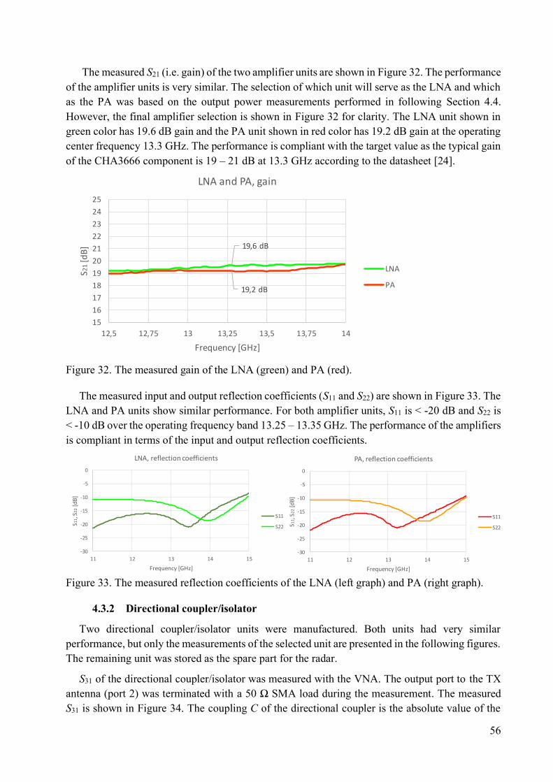
56
The measured S21 (i.e. gain) of the two amplifier units are shown in Figure 32. The performance
of the amplifier units is very similar. The selection of which unit will serve as the LNA and which
as the PA was based on the output power measurements performed in following Section 4.4.
However, the final amplifier selection is shown in Figure 32 for clarity. The LNA unit shown in
green color has 19.6 dB gain and the PA unit shown in red color has 19.2 dB gain at the operating
center frequency 13.3 GHz. The performance is compliant with the target value as the typical gain
of the CHA3666 component is 19 – 21 dB at 13.3 GHz according to the datasheet [24].
Figure 32. The measured gain of the LNA (green) and PA (red).
The measured input and output reflection coefficients (S11 and S22) are shown in Figure 33. The
LNA and PA units show similar performance. For both amplifier units, S11 is < -20 dB and S22 is
< -10 dB over the operating frequency band 13.25 – 13.35 GHz. The performance of the amplifiers
is compliant in terms of the input and output reflection coefficients.
Figure 33. The measured reflection coefficients of the LNA (left graph) and PA (right graph).
4.3.2 Directional coupler/isolator
Two directional coupler/isolator units were manufactured. Both units had very similar
performance, but only the measurements of the selected unit are presented in the following figures.
The remaining unit was stored as the spare part for the radar.
S31 of the directional coupler/isolator was measured with the VNA. The output port to the TX
antenna (port 2) was terminated with a 50 Ω SMA load during the measurement. The measured
S31 is shown in Figure 34. The coupling C of the directional coupler is the absolute value of the
19,6 dB
19,2 dB
15
16
17
18
19
20
21
22
23
24
25
12,5 12,75 13 13,25 13,5 13,75 14
S21
[dB
]
Frequency [GHz]
LNA and PA, gain
LNA
PA
-30
-25
-20
-15
-10
-5
0
11 12 13 14 15
S11, S
22
[dB
]
Frequency [GHz]
LNA, reflection coefficients
S11
S22
-30
-25
-20
-15
-10
-5
0
11 12 13 14 15
S11, S
22
[dB
]
Frequency [GHz]
PA, reflection coefficients
S11
S22
57
S31 (i.e. |S31|), and it is 15.5 dB at the operating center frequency 13.3 GHz. The simulated coupling
was 10.7 dB at 13.3 GHz (see Figure 16). The difference between the simulated and measured
performance is most likely due to the production tolerances of the PCB. The narrow gap (s = 0.12
µm) between the coupled lines determines the coupling of the directional coupler. If the gap is
wider than specified, the coupling gets worse. It was not required to use a space qualified PCB
manufacturer in the breadboarding phase of the project and thus an ordinary manufacturer was
used for economical reasons. It is expected that the performance of the directional coupler will
improve when higher manufacturing tolerances take place in the Engineering Model of the
altimeter.
The output power of the PA is approximately 16 dBm. The coupling C = 15.5 dB leads to higher
than 0 dBm LO port power for the mixer. This was considered high enough for the mixer diodes
and thus the measured coupling is compliant with the target value.
Figure 34. The measured S31 (coupling) of the directional coupler/isolator.
The measured S21 of the directional coupler/isolator is shown in Figure 35. A 50 Ω termination
was installed to port 3 of the coupler during the measurement. The absolute value of S21 is also the
insertion loss of the coupler. The measured insertion loss is 1.6 dB at the operating center
frequency 13.3 GHz. The simulated insertion loss was 0.7 dB. However, the drop-in isolator
NJ1140-07 was not included in the simulations. According to the datasheet of the isolator [28], the
isolator contributes approximately 0.8 dB to the total insertion loss value of the manufactured
coupler, and therefore the measured insertion loss of the directional coupler/isolator combination
is very close to the value expected from the simulations.
-15,5 dB
-20
-19
-18
-17
-16
-15
-14
-13
-12
-11
-10
11 11,5 12 12,5 13 13,5 14 14,5 15
S31
[dB
]
Frequency [GHz]
Directional coupler, S31 (coupling)
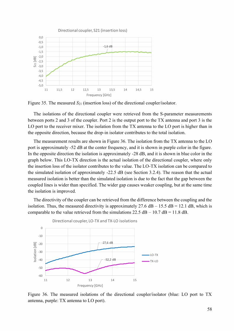
58
Figure 35. The measured S21 (insertion loss) of the directional coupler/isolator.
The isolations of the directional coupler were retrieved from the S-parameter measurements
between ports 2 and 3 of the coupler. Port 2 is the output port to the TX antenna and port 3 is the
LO port to the receiver mixer. The isolation from the TX antenna to the LO port is higher than in
the opposite direction, because the drop-in isolator contributes to the total isolation.
The measurement results are shown in Figure 36. The isolation from the TX antenna to the LO
port is approximately -52 dB at the center frequency, and it is shown in purple color in the figure.
In the opposite direction the isolation is approximately -28 dB, and it is shown in blue color in the
graph below. This LO-TX direction is the actual isolation of the directional coupler, where only
the insertion loss of the isolator contributes to the value. The LO-TX isolation can be compared to
the simulated isolation of approximately -22.5 dB (see Section 3.2.4). The reason that the actual
measured isolation is better than the simulated isolation is due to the fact that the gap between the
coupled lines is wider than specified. The wider gap causes weaker coupling, but at the same time
the isolation is improved.
The directivity of the coupler can be retrieved from the difference between the coupling and the
isolation. Thus, the measured directivity is approximately 27.6 dB – 15.5 dB = 12.1 dB, which is
comparable to the value retrieved from the simulations 22.5 dB – 10.7 dB = 11.8 dB.
Figure 36. The measured isolations of the directional coupler/isolator (blue: LO port to TX
antenna, purple: TX antenna to LO port).
-1,6 dB
-5,0
-4,5
-4,0
-3,5
-3,0
-2,5
-2,0
-1,5
-1,0
-0,5
0,0
11 11,5 12 12,5 13 13,5 14 14,5 15
S21
[dB
]
Frequency [GHz]
Directional coupler, S21 (insertion loss)
-27,6 dB
-52,2 dB
-60
-50
-40
-30
-20
-10
0
11 12 13 14 15
Iso
lati
on
[dB
]
Frequency [GHz]
Directional coupler, LO-TX and TX-LO isolations
LO-TX
TX-LO
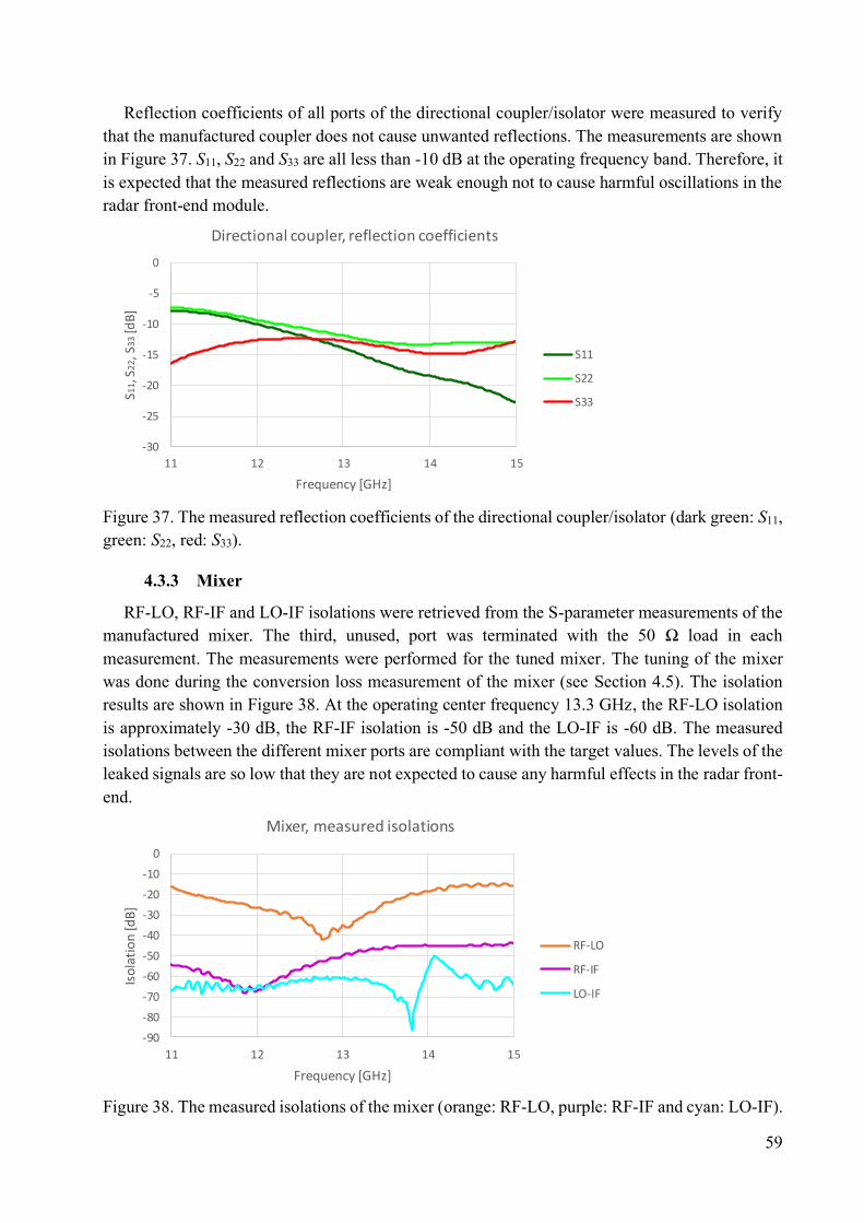
59
Reflection coefficients of all ports of the directional coupler/isolator were measured to verify
that the manufactured coupler does not cause unwanted reflections. The measurements are shown
in Figure 37. S11, S22 and S33 are all less than -10 dB at the operating frequency band. Therefore, it
is expected that the measured reflections are weak enough not to cause harmful oscillations in the
radar front-end module.
Figure 37. The measured reflection coefficients of the directional coupler/isolator (dark green: S11,
green: S22, red: S33).
4.3.3 Mixer
RF-LO, RF-IF and LO-IF isolations were retrieved from the S-parameter measurements of the
manufactured mixer. The third, unused, port was terminated with the 50 Ω load in each
measurement. The measurements were performed for the tuned mixer. The tuning of the mixer
was done during the conversion loss measurement of the mixer (see Section 4.5). The isolation
results are shown in Figure 38. At the operating center frequency 13.3 GHz, the RF-LO isolation
is approximately -30 dB, the RF-IF isolation is -50 dB and the LO-IF is -60 dB. The measured
isolations between the different mixer ports are compliant with the target values. The levels of the
leaked signals are so low that they are not expected to cause any harmful effects in the radar front-
end.
Figure 38. The measured isolations of the mixer (orange: RF-LO, purple: RF-IF and cyan: LO-IF).
-30
-25
-20
-15
-10
-5
0
11 12 13 14 15
S11, S
22, S
33[d
B]
Frequency [GHz]
Directional coupler, reflection coefficients
S11
S22
S33
-90
-80
-70
-60
-50
-40
-30
-20
-10
0
11 12 13 14 15
Iso
lati
on
[dB
]
Frequency [GHz]
Mixer, measured isolations
RF-LO
RF-IF
LO-IF
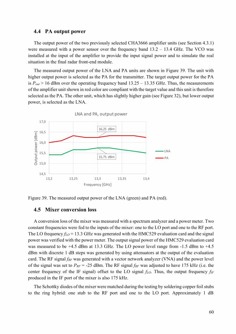
60
4.4 PA output power
The output power of the two previously selected CHA3666 amplifier units (see Section 4.3.1)
were measured with a power sensor over the frequency band 13.2 – 13.4 GHz. The VCO was
installed at the input of the amplifier to provide the input signal power and to simulate the real
situation in the final radar front-end module.
The measured output power of the LNA and PA units are shown in Figure 39. The unit with
higher output power is selected as the PA for the transmitter. The target output power for the PA
is Pout > 16 dBm over the operating frequency band 13.25 – 13.35 GHz. Thus, the measurements
of the amplifier unit shown in red color are compliant with the target value and this unit is therefore
selected as the PA. The other unit, which has slightly higher gain (see Figure 32), but lower output
power, is selected as the LNA.
Figure 39. The measured output power of the LNA (green) and PA (red).
4.5 Mixer conversion loss
A conversion loss of the mixer was measured with a spectrum analyzer and a power meter. Two
constant frequencies were fed to the inputs of the mixer: one to the LO port and one to the RF port.
The LO frequency fLO = 13.3 GHz was generated with the HMC529 evaluation card and the signal
power was verified with the power meter. The output signal power of the HMC529 evaluation card
was measured to be +4.5 dBm at 13.3 GHz. The LO power level range from -1.5 dBm to +4.5
dBm with discrete 1 dB steps was generated by using attenuators at the output of the evaluation
card. The RF signal fRF was generated with a vector network analyzer (VNA) and the power level
of the signal was set to PRF = -25 dBm. The RF signal fRF was adjusted to have 175 kHz (i.e. the
center frequency of the IF signal) offset to the LO signal fLO. Thus, the output frequency fIF
produced in the IF port of the mixer is also 175 kHz.
The Schottky diodes of the mixer were matched during the testing by soldering copper foil stubs
to the ring hybrid: one stub to the RF port and one to the LO port. Approximately 1 dB
15,75 dBm
16,25 dBm
14,5
15,0
15,5
16,0
16,5
17,0
13,2 13,25 13,3 13,35 13,4
Ou
tpu
t p
ow
er [d
Bm
]
Frequency [GHz]
LNA and PA, output power
LNA
PA
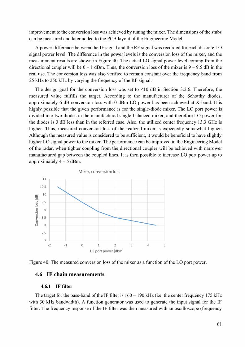
61
improvement to the conversion loss was achieved by tuning the mixer. The dimensions of the stubs
can be measured and later added to the PCB layout of the Engineering Model.
A power difference between the IF signal and the RF signal was recorded for each discrete LO
signal power level. The difference in the power levels is the conversion loss of the mixer, and the
measurement results are shown in Figure 40. The actual LO signal power level coming from the
directional coupler will be 0 – 1 dBm. Thus, the conversion loss of the mixer is 9 – 9.5 dB in the
real use. The conversion loss was also verified to remain constant over the frequency band from
25 kHz to 250 kHz by varying the frequency of the RF signal.
The design goal for the conversion loss was set to <10 dB in Section 3.2.6. Therefore, the
measured value fulfills the target. According to the manufacturer of the Schottky diodes,
approximately 6 dB conversion loss with 0 dBm LO power has been achieved at X-band. It is
highly possible that the given performance is for the single-diode mixer. The LO port power is
divided into two diodes in the manufactured single-balanced mixer, and therefore LO power for
the diodes is 3 dB less than in the referred case. Also, the utilized center frequency 13.3 GHz is
higher. Thus, measured conversion loss of the realized mixer is expectedly somewhat higher.
Although the measured value is considered to be sufficient, it would be beneficial to have slightly
higher LO signal power to the mixer. The performance can be improved in the Engineering Model
of the radar, when tighter coupling from the directional coupler will be achieved with narrower
manufactured gap between the coupled lines. It is then possible to increase LO port power up to
approximately 4 – 5 dBm.
Figure 40. The measured conversion loss of the mixer as a function of the LO port power.
4.6 IF chain measurements
4.6.1 IF filter
The target for the pass-band of the IF filter is 160 – 190 kHz (i.e. the center frequency 175 kHz
with 30 kHz bandwidth). A function generator was used to generate the input signal for the IF
filter. The frequency response of the IF filter was then measured with an oscilloscope (frequency
7
7,5
8
8,5
9
9,5
10
10,5
11
-2 -1 0 1 2 3 4 5
Co
nve
rsio
n lo
ss [d
B]
LO port power [dBm]
Mixer, conversion loss
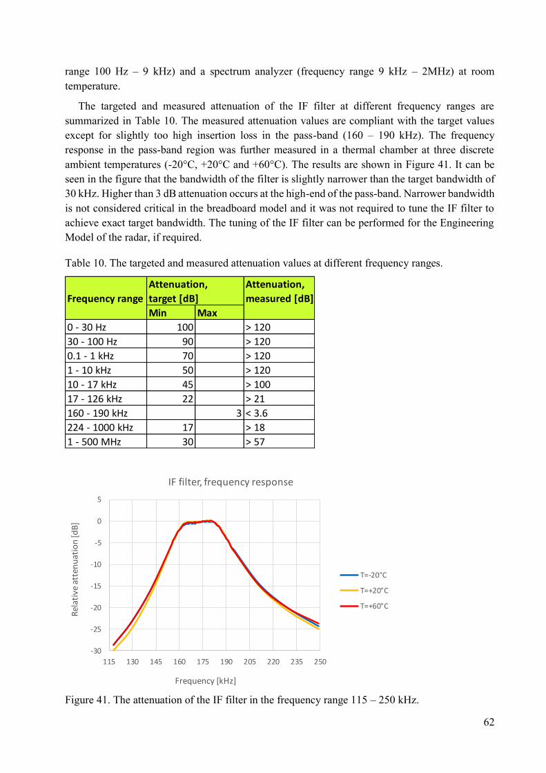
62
range 100 Hz – 9 kHz) and a spectrum analyzer (frequency range 9 kHz – 2MHz) at room
temperature.
The targeted and measured attenuation of the IF filter at different frequency ranges are
summarized in Table 10. The measured attenuation values are compliant with the target values
except for slightly too high insertion loss in the pass-band (160 – 190 kHz). The frequency
response in the pass-band region was further measured in a thermal chamber at three discrete
ambient temperatures (-20°C, +20°C and +60°C). The results are shown in Figure 41. It can be
seen in the figure that the bandwidth of the filter is slightly narrower than the target bandwidth of
30 kHz. Higher than 3 dB attenuation occurs at the high-end of the pass-band. Narrower bandwidth
is not considered critical in the breadboard model and it was not required to tune the IF filter to
achieve exact target bandwidth. The tuning of the IF filter can be performed for the Engineering
Model of the radar, if required.
Table 10. The targeted and measured attenuation values at different frequency ranges.
Figure 41. The attenuation of the IF filter in the frequency range 115 – 250 kHz.
Attenuation, Attenuation,
Frequency range target [dB] measured [dB]
Min Max
0 - 30 Hz 100 > 120
30 - 100 Hz 90 > 120
0.1 - 1 kHz 70 > 120
1 - 10 kHz 50 > 120
10 - 17 kHz 45 > 100
17 - 126 kHz 22 > 21
160 - 190 kHz 3 < 3.6
224 - 1000 kHz 17 > 18
1 - 500 MHz 30 > 57
-30
-25
-20
-15
-10
-5
0
5
115 130 145 160 175 190 205 220 235 250
Rel
ativ
e at
ten
uat
ion
[dB
]
Frequency [kHz]
IF filter, frequency response
T=-20°C
T=+20°C
T=+60°C
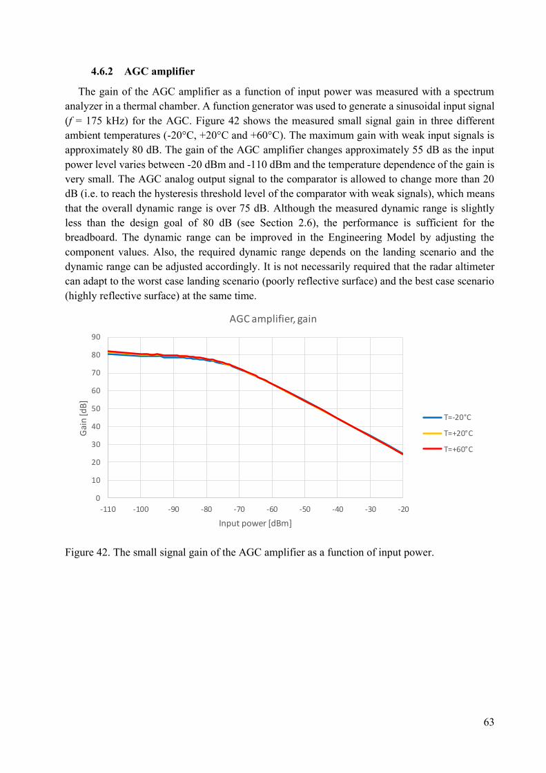
63
4.6.2 AGC amplifier
The gain of the AGC amplifier as a function of input power was measured with a spectrum
analyzer in a thermal chamber. A function generator was used to generate a sinusoidal input signal
(f = 175 kHz) for the AGC. Figure 42 shows the measured small signal gain in three different
ambient temperatures (-20°C, +20°C and +60°C). The maximum gain with weak input signals is
approximately 80 dB. The gain of the AGC amplifier changes approximately 55 dB as the input
power level varies between -20 dBm and -110 dBm and the temperature dependence of the gain is
very small. The AGC analog output signal to the comparator is allowed to change more than 20
dB (i.e. to reach the hysteresis threshold level of the comparator with weak signals), which means
that the overall dynamic range is over 75 dB. Although the measured dynamic range is slightly
less than the design goal of 80 dB (see Section 2.6), the performance is sufficient for the
breadboard. The dynamic range can be improved in the Engineering Model by adjusting the
component values. Also, the required dynamic range depends on the landing scenario and the
dynamic range can be adjusted accordingly. It is not necessarily required that the radar altimeter
can adapt to the worst case landing scenario (poorly reflective surface) and the best case scenario
(highly reflective surface) at the same time.
Figure 42. The small signal gain of the AGC amplifier as a function of input power.
0
10
20
30
40
50
60
70
80
90
-110 -100 -90 -80 -70 -60 -50 -40 -30 -20
Gai
n [d
B]
Input power [dBm]
AGC amplifier, gain
T=-20°C
T=+20°C
T=+60°C
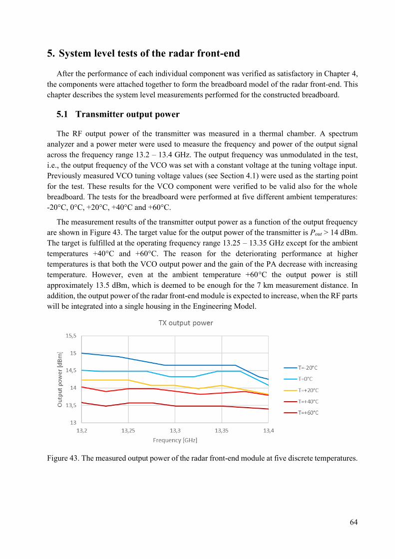
64
5. System level tests of the radar front-end
After the performance of each individual component was verified as satisfactory in Chapter 4,
the components were attached together to form the breadboard model of the radar front-end. This
chapter describes the system level measurements performed for the constructed breadboard.
5.1 Transmitter output power
The RF output power of the transmitter was measured in a thermal chamber. A spectrum
analyzer and a power meter were used to measure the frequency and power of the output signal
across the frequency range 13.2 – 13.4 GHz. The output frequency was unmodulated in the test,
i.e., the output frequency of the VCO was set with a constant voltage at the tuning voltage input.
Previously measured VCO tuning voltage values (see Section 4.1) were used as the starting point
for the test. These results for the VCO component were verified to be valid also for the whole
breadboard. The tests for the breadboard were performed at five different ambient temperatures:
-20°C, 0°C, +20°C, +40°C and +60°C.
The measurement results of the transmitter output power as a function of the output frequency
are shown in Figure 43. The target value for the output power of the transmitter is Pout > 14 dBm.
The target is fulfilled at the operating frequency range 13.25 – 13.35 GHz except for the ambient
temperatures +40°C and +60°C. The reason for the deteriorating performance at higher
temperatures is that both the VCO output power and the gain of the PA decrease with increasing
temperature. However, even at the ambient temperature +60°C the output power is still
approximately 13.5 dBm, which is deemed to be enough for the 7 km measurement distance. In
addition, the output power of the radar front-end module is expected to increase, when the RF parts
will be integrated into a single housing in the Engineering Model.
Figure 43. The measured output power of the radar front-end module at five discrete temperatures.
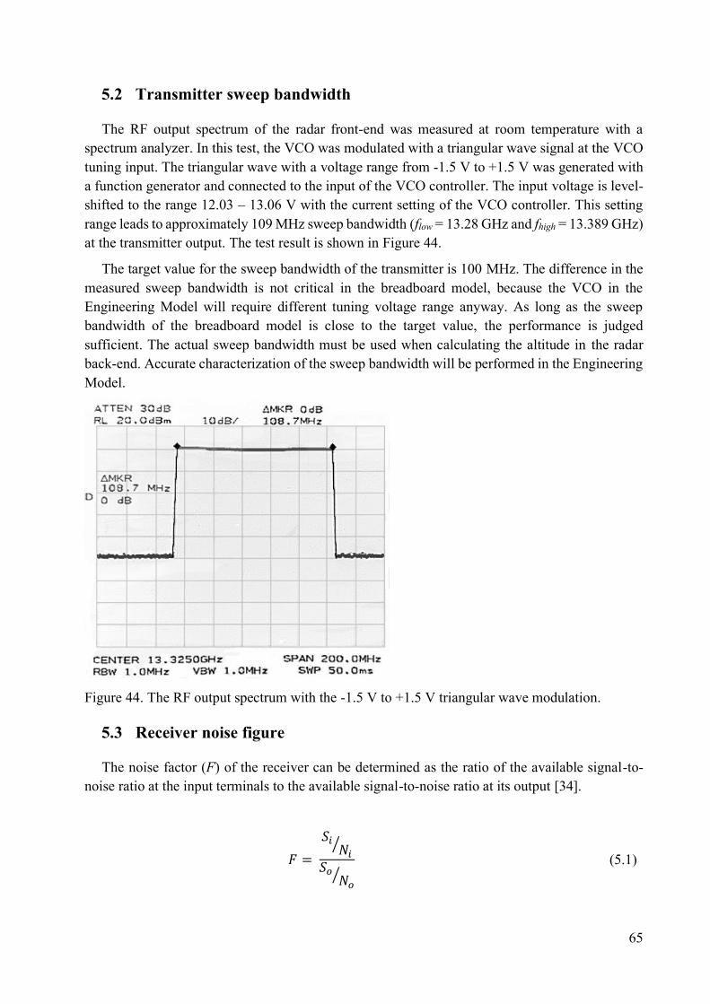
65
5.2 Transmitter sweep bandwidth
The RF output spectrum of the radar front-end was measured at room temperature with a
spectrum analyzer. In this test, the VCO was modulated with a triangular wave signal at the VCO
tuning input. The triangular wave with a voltage range from -1.5 V to +1.5 V was generated with
a function generator and connected to the input of the VCO controller. The input voltage is level-
shifted to the range 12.03 – 13.06 V with the current setting of the VCO controller. This setting
range leads to approximately 109 MHz sweep bandwidth (flow = 13.28 GHz and fhigh = 13.389 GHz)
at the transmitter output. The test result is shown in Figure 44.
The target value for the sweep bandwidth of the transmitter is 100 MHz. The difference in the
measured sweep bandwidth is not critical in the breadboard model, because the VCO in the
Engineering Model will require different tuning voltage range anyway. As long as the sweep
bandwidth of the breadboard model is close to the target value, the performance is judged
sufficient. The actual sweep bandwidth must be used when calculating the altitude in the radar
back-end. Accurate characterization of the sweep bandwidth will be performed in the Engineering
Model.
Figure 44. The RF output spectrum with the -1.5 V to +1.5 V triangular wave modulation.
5.3 Receiver noise figure
The noise factor (F) of the receiver can be determined as the ratio of the available signal-to-
noise ratio at the input terminals to the available signal-to-noise ratio at its output [34].
𝐹 =
𝑆𝑖𝑁𝑖
⁄
𝑆𝑜𝑁𝑜
⁄ (5.1)
66
The VCO of the radar front-end was set to provide constant center frequency (13.3 GHz). A
signal generator was used to inject a known signal power to the input of the receiver. The frequency
of the input signal had 175 kHz offset to the output frequency of the VCO so that the correct beat
frequency was obtained at the output of the receiver. The input signal power must be set to a low
value (approximately -110 dBm), so that the AGC amplifier of the receiver is providing full
constant gain.
The power of the injected input signal was measured with a spectrum analyzer (the resolution
bandwidth of the spectrum analyzer was set to 1 kHz). Then the noise level of the signal generator
was measured in the absence of the signal. This way, the signal-to-noise ratio (SNR) at the input
of the receiver could be determined. The same procedure was used to determine the SNR at the
output of the receiver by connecting the spectrum analyzer to the analog IF output of the radar
front-end. Now, the noise figure (NF) can be calculated from the difference between the input and
output SNR.
𝑁𝐹 = 𝑆𝑖
𝑁𝑖−
𝑆𝑜
𝑁𝑜= 6.5 dB
The used method is rather inaccurate, because the measured signal and noise levels are very
low. The measured receiver noise figure can be compared to the theoretical value. The noise factor
for the cascaded receiver chain can be calculated from:
𝐹𝑟𝑒𝑐 = 𝐹𝐿𝑁𝐴 +𝐹𝑚𝑖𝑥𝑒𝑟 − 1
𝐺𝐿𝑁𝐴+
𝐿𝑚𝑖𝑥𝑒𝑟(𝐹𝐼𝐹 − 1)
𝐺𝐿𝑁𝐴 (5.2)
The LNA gain was measured to be GLNA = 19.6 dB and the mixer conversion loss Lmixer = 9 dB.
For a passive mixer without any gain, the noise figure is almost the same as the conversion loss,
i.e. NFmixer ≃ 9 dB. The noise figures of the LNA and the IF chain (i.e. AGC amplifier) were not
measured, but the noise figures can be estimated from the datasheets of the amplifiers (LNA:
CHA3666 and AGC: 2N5551). Thus, the noise figure of the LNA is approximately NFLNA = 2 dB
and the noise figure of the IF chain is approximately NFIF = 8 dB. Inserting these values into
equation (5.2), solving the receiver noise figure (NFrec = 10logFrec) and adding 3 dB for the noise
coming from the image frequency leads to the receiver noise figure NFrec = 6.3 dB. Although the
measured noise figure 6.5 dB is considered inaccurate, it is close enough to the calculated value.
The receiver noise figure used to predict the radar range was 6 dB (see Section 2.6, Table 5).
The difference in the measured value does not degrade the range much, and the range is still
expected to be larger than 7 km even in the case of poorly reflective surface. Therefore, further
investigation regarding to the noise figure of the receiver was not required and the performance of
the receiver is as expected.
The best solution to improve the noise figure of the receiver would be to use the image rejection
mixer instead of the single-balanced mixer. However, this was not an option in this application
67
due to the power consumption reasons. Therefore, the second best option is to improve the mixer
conversion loss in the Engineering Model. This can be achieved by increasing the LO port power
coming from the directional coupler.
5.4 Power consumption, size and mass
The requirement for the power consumption is < 2.5 W over the full operational temperature
range of the breadboard (-20°C to +60°C). The radar front-end module was measured in a thermal
chamber at three discrete ambient temperatures: -20°C, +20°C and +60°C. The power
consumption was determined by measuring the operating voltages and currents, while the radar
front-end was fully powered on. The AGC amplifier was providing full gain, and thus consuming
the maximum amount of power.
The measured values at three operating temperatures are summarized in Table 11. The power
consumption is less than 2.5 W over the required temperature range, and thus compliant with the
target. The measured value 2.4 W at room temperature is also comparable to the power
consumption 2.44 W previously estimated from the datasheets of the individual components.
Table 11. The measured power consumption of the radar front-end.
The physical dimensions of the radar front-end module were measured with a caliber. The
measured dimensions are 145.5 x 95.9 x 68 mm3, and thus compliant with the maximum target
dimensions 150 x 100 x 70 mm3.
The mass of the radar front-end module was measured with a weight scale. The measured mass
is 526 g, and thus compliant with the maximum target mass 0.67 kg.
5.5 Functionality tests of the radar front-end
In order to test the functionality of the radar front-end in laboratory conditions, an Electric
Ground Support Equipment (EGSE) was developed by Harp Technologies. The EGSE provides
11 different time delays and an adjustable step attenuator to simulate 11 different altitudes and
different backscattering coefficients (σ0) for all of them. The shortest delay (i.e. 10 m measurement
altitude) is implemented using a coaxial cable and all the other delays are generated with SAW
filter delay lines.
Table 12 shows the measured average delay values of the EGSE over the operational
bandwidth, and the corresponding approximate altitudes. The path loss with the nominal
backscattering coefficient σ0 = 6 dB is also presented in the table. The attenuation value can be
adjusted ±15 dB with the EGSE step attenuator. The theoretical frequency of the modulating signal
Temperature
Estimated Measured
-20°C - 2446 mW
+20°C 2440 mW 2398 mW
+60°C - 2332 mW
Power consumption
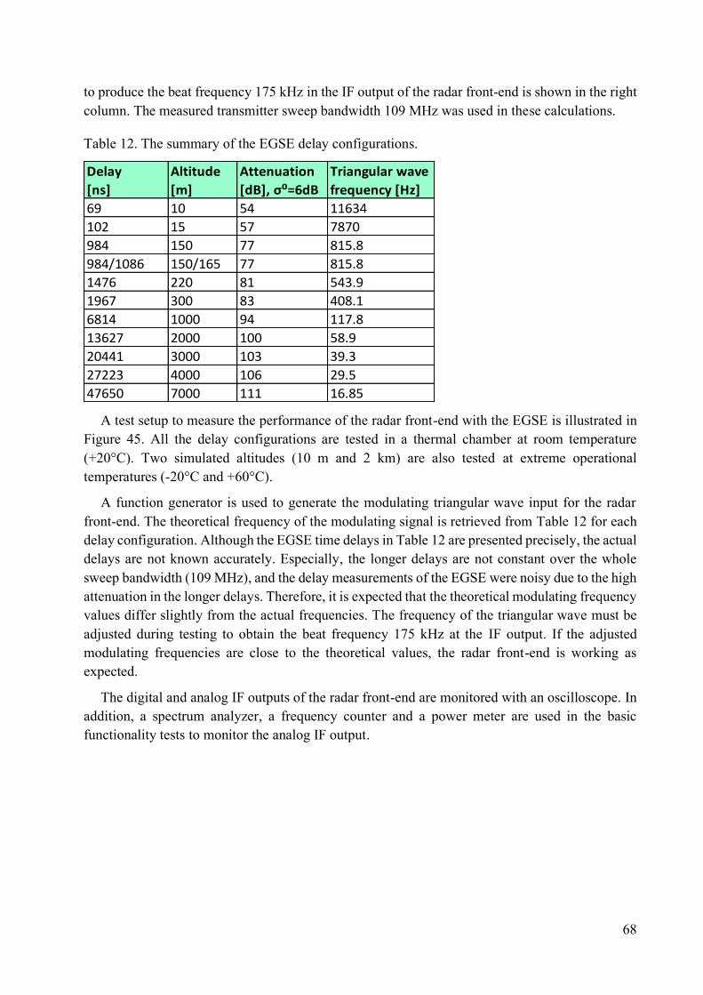
68
to produce the beat frequency 175 kHz in the IF output of the radar front-end is shown in the right
column. The measured transmitter sweep bandwidth 109 MHz was used in these calculations.
Table 12. The summary of the EGSE delay configurations.
Delay Altitude Attenuation Triangular wave
[ns] [m] [dB], σ⁰=6dB frequency [Hz]
69 10 54 11634
102 15 57 7870
984 150 77 815.8
984/1086 150/165 77 815.8
1476 220 81 543.9
1967 300 83 408.1
6814 1000 94 117.8
13627 2000 100 58.9
20441 3000 103 39.3
27223 4000 106 29.5
47650 7000 111 16.85
A test setup to measure the performance of the radar front-end with the EGSE is illustrated in
Figure 45. All the delay configurations are tested in a thermal chamber at room temperature
(+20°C). Two simulated altitudes (10 m and 2 km) are also tested at extreme operational
temperatures (-20°C and +60°C).
A function generator is used to generate the modulating triangular wave input for the radar
front-end. The theoretical frequency of the modulating signal is retrieved from Table 12 for each
delay configuration. Although the EGSE time delays in Table 12 are presented precisely, the actual
delays are not known accurately. Especially, the longer delays are not constant over the whole
sweep bandwidth (109 MHz), and the delay measurements of the EGSE were noisy due to the high
attenuation in the longer delays. Therefore, it is expected that the theoretical modulating frequency
values differ slightly from the actual frequencies. The frequency of the triangular wave must be
adjusted during testing to obtain the beat frequency 175 kHz at the IF output. If the adjusted
modulating frequencies are close to the theoretical values, the radar front-end is working as
expected.
The digital and analog IF outputs of the radar front-end are monitored with an oscilloscope. In
addition, a spectrum analyzer, a frequency counter and a power meter are used in the basic
functionality tests to monitor the analog IF output.
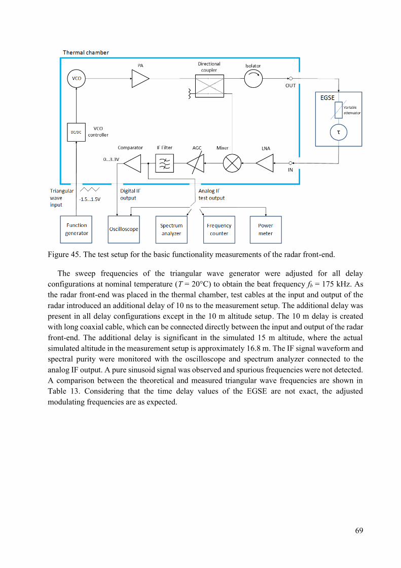
69
Figure 45. The test setup for the basic functionality measurements of the radar front-end.
The sweep frequencies of the triangular wave generator were adjusted for all delay
configurations at nominal temperature (T = 20°C) to obtain the beat frequency fb = 175 kHz. As
the radar front-end was placed in the thermal chamber, test cables at the input and output of the
radar introduced an additional delay of 10 ns to the measurement setup. The additional delay was
present in all delay configurations except in the 10 m altitude setup. The 10 m delay is created
with long coaxial cable, which can be connected directly between the input and output of the radar
front-end. The additional delay is significant in the simulated 15 m altitude, where the actual
simulated altitude in the measurement setup is approximately 16.8 m. The IF signal waveform and
spectral purity were monitored with the oscilloscope and spectrum analyzer connected to the
analog IF output. A pure sinusoid signal was observed and spurious frequencies were not detected.
A comparison between the theoretical and measured triangular wave frequencies are shown in
Table 13. Considering that the time delay values of the EGSE are not exact, the adjusted
modulating frequencies are as expected.
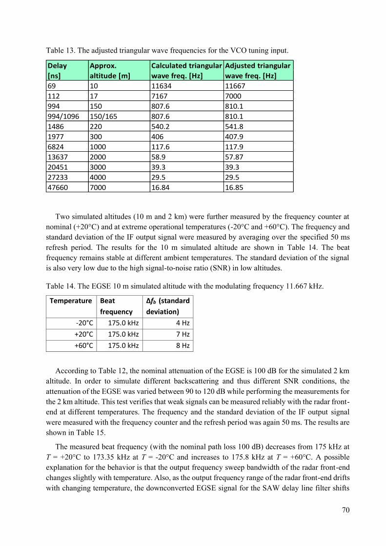
70
Table 13. The adjusted triangular wave frequencies for the VCO tuning input.
Delay Approx. Calculated triangular Adjusted triangular
[ns] altitude [m] wave freq. [Hz] wave freq. [Hz]
69 10 11634 11667
112 17 7167 7000
994 150 807.6 810.1
994/1096 150/165 807.6 810.1
1486 220 540.2 541.8
1977 300 406 407.9
6824 1000 117.6 117.9
13637 2000 58.9 57.87
20451 3000 39.3 39.3
27233 4000 29.5 29.5
47660 7000 16.84 16.85
Two simulated altitudes (10 m and 2 km) were further measured by the frequency counter at
nominal (+20°C) and at extreme operational temperatures (-20°C and +60°C). The frequency and
standard deviation of the IF output signal were measured by averaging over the specified 50 ms
refresh period. The results for the 10 m simulated altitude are shown in Table 14. The beat
frequency remains stable at different ambient temperatures. The standard deviation of the signal
is also very low due to the high signal-to-noise ratio (SNR) in low altitudes.
Table 14. The EGSE 10 m simulated altitude with the modulating frequency 11.667 kHz.
Temperature Beat
frequency
Δfb (standard
deviation)
-20°C 175.0 kHz 4 Hz
+20°C 175.0 kHz 7 Hz
+60°C 175.0 kHz 8 Hz
According to Table 12, the nominal attenuation of the EGSE is 100 dB for the simulated 2 km
altitude. In order to simulate different backscattering and thus different SNR conditions, the
attenuation of the EGSE was varied between 90 to 120 dB while performing the measurements for
the 2 km altitude. This test verifies that weak signals can be measured reliably with the radar front-
end at different temperatures. The frequency and the standard deviation of the IF output signal
were measured with the frequency counter and the refresh period was again 50 ms. The results are
shown in Table 15.
The measured beat frequency (with the nominal path loss 100 dB) decreases from 175 kHz at
T = +20°C to 173.35 kHz at T = -20°C and increases to 175.8 kHz at T = +60°C. A possible
explanation for the behavior is that the output frequency sweep bandwidth of the radar front-end
changes slightly with temperature. Also, as the output frequency range of the radar front-end drifts
with changing temperature, the downconverted EGSE signal for the SAW delay line filter shifts
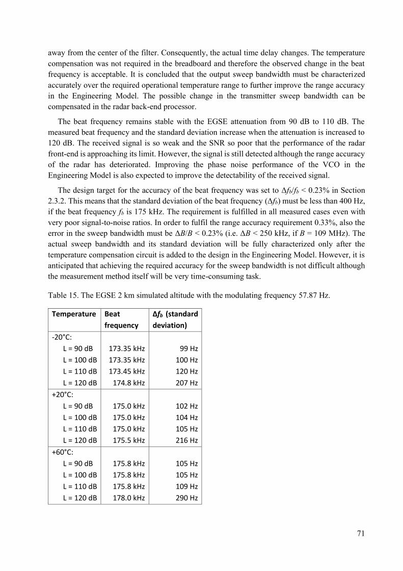
71
away from the center of the filter. Consequently, the actual time delay changes. The temperature
compensation was not required in the breadboard and therefore the observed change in the beat
frequency is acceptable. It is concluded that the output sweep bandwidth must be characterized
accurately over the required operational temperature range to further improve the range accuracy
in the Engineering Model. The possible change in the transmitter sweep bandwidth can be
compensated in the radar back-end processor.
The beat frequency remains stable with the EGSE attenuation from 90 dB to 110 dB. The
measured beat frequency and the standard deviation increase when the attenuation is increased to
120 dB. The received signal is so weak and the SNR so poor that the performance of the radar
front-end is approaching its limit. However, the signal is still detected although the range accuracy
of the radar has deteriorated. Improving the phase noise performance of the VCO in the
Engineering Model is also expected to improve the detectability of the received signal.
The design target for the accuracy of the beat frequency was set to Δfb/fb < 0.23% in Section
2.3.2. This means that the standard deviation of the beat frequency (Δfb) must be less than 400 Hz,
if the beat frequency fb is 175 kHz. The requirement is fulfilled in all measured cases even with
very poor signal-to-noise ratios. In order to fulfil the range accuracy requirement 0.33%, also the
error in the sweep bandwidth must be ΔB/B < 0.23% (i.e. ΔB < 250 kHz, if B = 109 MHz). The
actual sweep bandwidth and its standard deviation will be fully characterized only after the
temperature compensation circuit is added to the design in the Engineering Model. However, it is
anticipated that achieving the required accuracy for the sweep bandwidth is not difficult although
the measurement method itself will be very time-consuming task.
Table 15. The EGSE 2 km simulated altitude with the modulating frequency 57.87 Hz.
Temperature Beat
frequency
Δfb (standard
deviation)
-20°C:
L = 90 dB
L = 100 dB
L = 110 dB
L = 120 dB
173.35 kHz
173.35 kHz
173.45 kHz
174.8 kHz
99 Hz
100 Hz
120 Hz
207 Hz
+20°C:
L = 90 dB
L = 100 dB
L = 110 dB
L = 120 dB
175.0 kHz
175.0 kHz
175.0 kHz
175.5 kHz
102 Hz
104 Hz
105 Hz
216 Hz
+60°C:
L = 90 dB
L = 100 dB
L = 110 dB
L = 120 dB
175.8 kHz
175.8 kHz
175.8 kHz
178.0 kHz
105 Hz
105 Hz
109 Hz
290 Hz
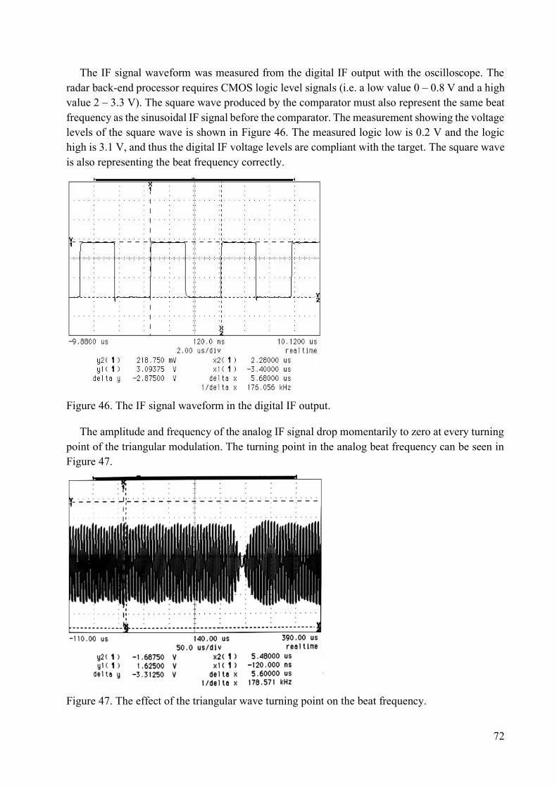
72
The IF signal waveform was measured from the digital IF output with the oscilloscope. The
radar back-end processor requires CMOS logic level signals (i.e. a low value 0 – 0.8 V and a high
value 2 – 3.3 V). The square wave produced by the comparator must also represent the same beat
frequency as the sinusoidal IF signal before the comparator. The measurement showing the voltage
levels of the square wave is shown in Figure 46. The measured logic low is 0.2 V and the logic
high is 3.1 V, and thus the digital IF voltage levels are compliant with the target. The square wave
is also representing the beat frequency correctly.
Figure 46. The IF signal waveform in the digital IF output.
The amplitude and frequency of the analog IF signal drop momentarily to zero at every turning
point of the triangular modulation. The turning point in the analog beat frequency can be seen in
Figure 47.
Figure 47. The effect of the triangular wave turning point on the beat frequency.
73
Figure 48 shows a closer view of the analog and digital IF output signals and what happens in
the digital IF signal when the analog signal disappears momentarily. This example was performed
with the simulated 10 m altitude of the EGSE and the analog and digital IF outputs were monitored
with the oscilloscope. The lower signal (channel 1 of the oscilloscope) in the figure shows the
analog IF signal and the higher signal (channel 2) shows the respective digital IF signal. As the
analog IF signal disappears momentarily, the digital IF signal stays at the high value. Depending
on the phase of the analog signal, the digital output may also stay at the low value during the
transition. The radar back-end processor calculates the number of square wave pulses received
during the refresh period (50 ms) and retrieves the beat frequency from it. If the phenomenon seen
in Figure 48 is not taken into account, a systematic error in the calculated beat frequency may
occur.
The worst case scenario happens if the threshold levels of the comparator are not set correctly.
In that case, even very weak analog signal may be enough to change the state of the digital signal
during transition period, and as a consequence an additional short square wave pulse appears. At
the lowest 10 m altitude (where the modulating frequency is 11.67 kHz), the calculated beat
frequency would change from the actual 175 kHz to 186.67 kHz. Thus, there is an absolute error
of approximately 0.7 m in the measured altitude. At higher altitudes the relative error decreases,
because the modulating frequency is then lower. It is concluded that special care must be taken
when testing and tuning the Engineering Model of the altimeter to remove systematic errors in the
altitude extraction.
Figure 48. The analog and digital beat frequencies in the outputs of the radar front-end. Channel 1
(lower) is the analog IF output (1 V/div, offset 1.75 V) and channel 2 (higher) is the digital IF
output (1 V/div, offset 0 V).
74
6. Conclusions
The European Space Agency has identified a demand for small landers in upcoming scientific
Mars missions. Therefore, size, mass and power consumption of all necessary sensors onboard the
lander have to be minimized. These drastic requirements apply also to an altimeter sensor, which
is used to measure a ground distance during descent and landing.
A development philosophy in a space project is to prove first a feasibility of chosen technology
with a breadboard model. Commercial-of-the-shelf (COTS) components, which have space
qualified equivalents, can be used in the breadboard model. If the operational requirements are
fulfilled with the breadboard, the project can advance to the Engineering Model and finally to the
Flight Model.
The development of the breadboard model of the radar altimeter front-end was described in this
thesis. Pulse and FMCW radars have strong space heritage in planetary exploration missions. Both
technological choices were assessed and the FMCW radar technology was selected for further
development. The radar is required to measure the ground distance reliably from the 7 km altitude
down to 10 m. As the power consumption requirement for the radar front-end is only 2.5 W,
fulfilling the maximum range requirement with the pulse radar was seen too problematic.
A choice of operational frequency in this project depends mainly on the maximum allowed size
of the radar and the availability of European space qualified components. Ku-band frequency was
evaluated to be the most suitable for this application. In order to test the radar altimeter on Earth,
an authorized frequency band was selected leading to the operational center frequency 13.3 GHz
with 100 MHz sweep bandwidth. The servo-type FMCW radar technology, where the ramp rate
of the frequency sweep is constantly modified, was chosen in order to improve the signal-to-noise
ratio of the receiver. The beat frequency is kept constant at 175 kHz by adjusting the ramp rate.
The IF bandwidth of the receiver is 30 kHz, which ensures that the anticipated Doppler shifted
frequencies fall within the IF band.
The Hagfors model was used to estimate the radar backscattering from the ground surface. The
Hagfors model usually shows good agreement with real measurement data of planetary objects.
Based on the published surface parameters for Mars, three different landing scenarios were
investigated: poorly reflective, typical, and highly reflective surfaces.
System parameters, such as the transmit power, antenna gain and receiver noise figure, were
estimated from the functional requirements for the altimeter. Using the assumed parameters, the
maximum predicted range of the FMCW radar was analysed for the poorly reflective and typically
reflective cases. The analysis revealed that approximately 13 dBm transmit power is required to
fulfil the range requirement in the poorly reflective measurement conditions. The system
parameters used in the range prediction were set as the target values for the radar design. These
target values can be improved, if it is noticed during the design phase that the functional
requirements (especially power consumption) have margin to do it.
A system level design of the FMCW radar front-end was performed and technical realisation
for each functional component was chosen. The individual components were then designed in to
their own housings in order to measure and tune the components before assembling the breadboard
75
model. The manufactured VCO component showed some sensitivity to RFI, which implied a
design change for the following Engineering Model. The triangular wave generator is currently
located in the radar back-end and it will be brought to the radar front-end in the EM. This will
improve the performance of the VCO. The PA and LNA were based on the same design, because
it was estimated that the output power of the LNA component is high-enough for the transmitter.
The selected component has also very low power consumption, which is an important factor in
this planetary altimeter application. Tight coupling required for the directional coupler causes
challenges in production. The performance can be improved, if the gap between the coupled lines
is etched accurately. A passive, single-balanced structure was chosen for the mixer. Using this
structure is beneficial in terms of power consumption, but it degrades the SNR of the receiver
approximately 3 dB compared to the image rejection mixer.
After the performance of the individual components had been verified, the breadboard model
of the radar front-end was constructed. The breadboard consists of three decks, which are
assembled in the housing provided by the prime contractor, Efacec.
The mass of the manufactured radar front-end is approximately 0.5 kg and the power
consumption is less than 2.5 W. The output power of the transmitter is approximately 14 dBm and
the output frequency range is 13.28 – 13.389 GHz at room temperature. These values are
temperature dependent, but temperature compensation will be implemented in the Engineering
Model. The noise figure of the receiver was measured to be approximately 6.5 dB.
A final verification of the radar front-end was done with an Electric Ground Support
Equipment. The EGSE simulates 11 different altitudes by introducing a time delay and attenuation
to the transmitted signal. Different backscattering conditions can also be inspected by adjusting
the attenuation value of each simulated altitude. The performance of the radar front-end was
satisfactory in all simulated altitudes. A disappearance of the beat frequency during the turn
periods of the triangular wave may cause systematic error in the calculated beat frequency. This
can be solved by signal processing techniques. If necessary, a blanking signal can be generated
from the analog IF signal. It can be used to discard the non-informative parts of the beat frequency.
The developed breadboard model fulfils the functional requirements for the radar altimeter. The
project can continue to the next phase, the Engineering Model. Integrating the RF components in
the same housing and introducing some minor changes to them will further improve the
performance of the radar front-end.
76
References
[1] Assessment and Bread-boarding of a Planetary Altimeter (ABPA), Statement of
Work, Issue 2.0, ABPA-SoW-ECN-20101026, European Space Agency, December
6, 2010.
[2] G. Brooker, Introduction to Sensors for Ranging and Imaging, SciTech Publishing,
2009.
[3] V. Rosmorduc et al, Radar altimetry tutorial, ESA/CNES Publication, Issue 3a, June
2018.
[4] Honeywell, “Honeywell HG8500 Series Radar Altimeter,” datasheet, DFOISR # 03-
S-1426, dated 13.6.2003.
[5] B. D. Pollard and C. W. Chen, “A Radar Terminal Descent Sensor for the Mars
Science Laboratory mission,” Proceedings of the 2009 IEEE Aerospace Conference,
2009.
[6] N. Hughes, “Story of Huygens radar altimeter,” Avaruusluotain, pp. 14-18, 4/2006.
[7] R. Trautner et al, “FMCW radars for entry probes and landers: Lessons learned from
the Huygens radar altimeter,” Proceedings of the 3rd International Workshop on
Planeterary Probes, published as ESA-SP 607, 2005.
[8] J. Griffiths, Radio Wave Propagation and Antennas: An Introduction, Prentice-Hall
International, 1987.
[9] M. Skolnik, Radar Handbook, 3rd edition, McGraw-Hill, 2008.
[10] F. E. Nathanson, Radar Design Principles, 2nd edition, SciTech Publishing, 1999.
[11] T. Hagfors, ”Backscattering from an undulating surface with applications to radar
returns from the Moon,” Journal of Geophysical Research, vol. 69, no. 18, pp. 3779-
3784, 1964.
[12] B. A. Campbell, Radar Remote Sensing of Planetary Surfaces, Cambridge
University Press, 2002.
[13] B. A. Campbell and M. K. Shepard, “Coherent and incoherent components in near-
nadir radar scattering: Applications to radar sounding of Mars,” Journal of
Geophysical Research, vol. 108, no. E12, 6-1 – 6-8, 2003.
[14] R. A. Simpson, “Spacecraft studies of planetary surfaces using bistatic radar,” IEEE
Transactions on Geoscience and Remote Sensing, vol. 31, no. 2, pp. 465-482, 1993.
[15] D. E. Smith et al, “Mars Orbiter Laser Altimeter: Experiment summary after the first
year of global mapping of Mars,” Journal of Geophysical Research, vol. 106, no.
E10, pp. 23,689-23,722, 2001.
[16] International Telecommunication Union, “Radio Regulations: Articles,” vol. 1,
2008.
[17] C. Ho, N. Golshan and A. Kliore, Radio Wave Propagation Handbook for
Communication on and Aroud Mars, Jet Propulsion Laboratory Publication 02-5,
2002.
77
[18] J. D. Kraus and R. J. Marhefka, Antennas for All Applications, 3rd edition, McGraw-
Hill, 2003.
[19] A. Räisänen and A. Lehto, Radiotekniikka, 7. painos, Otatieto Oy, 1996.
[20] F. T. Ulaby, R. K. Moore and A. K. Fung, Microwave Remote Sensing, Active and
Passive, Volume II, Artech House, 1982.
[21] D. C. Schlerer, MTI and Pulsed Doppler Radar with MATLAB, 2nd edition, Artech
House, 2010.
[22] Rogers Corporation, “RT/duroid 6002 High Frequency Laminates,” datasheet,
1.6002.
[23] Hittite Microwave Corporation, ”MMIC VCO w/ half frequency output & divide-
by-4, 12.4 – 13.4 GHz,” datasheet, v04.0811.
[24] United Monolithic Semiconductor, “5.8 – 17 GHz Low Noise Amplifier,” datasheet,
DSCHA3666-QAG8108, April 17, 2008.
[25] R. K. Mongia, I. J. Bahl, P. Bhartia, and J. Hong, RF and Microwave Coupled-Line
Circuits, 2nd edition, Artech House, 2007.
[26] A. Podell, “A high directivity microstrip coupler technique,” IEEE MTT-S
International Microwave Symposium Digest, pp. 33-36, May 1970.
[27] European Cooperation for Space Standardization, “Space product assurance –
Design rules for printed circuit boards,” ECSS-Q-ST-70-12C, July 2014.
[28] Cobham Microwave, “Dropin isolator clockwise version 13200 – 13400 MHz,”
datasheet for NJ1140-07, May 11, 2010.
[29] S. A. Maas, Nonlinear Microwave and RF Circuits, 2nd edition, Artech House, 2003.
[30] S. A. Maas, Microwave Mixers, 2nd edition, Artech House, 1993.
[31] L. E. Larson, RF and Microwave Circuit Design for Wireless Communications,
Artech House, 1996.
[32] European Preferred Parts List, Issue 23, 21.6.2013.
[33] International Telecommunication Union, “Assessment on use of spectrum in the 10-
17 GHz frequency band for the GSO fixed-satellite service in Region 1,” Report
ITU-R S.2365-0, 09/2015.
[34] H. T. Friis, “Noise figures of radio receivers,” Proceedings IRE, vol. 32, no. 7, pp.
419-422, July 1944.