Embed Size (px)
Citation preview
electronics
Article
A Power Efficient Frequency Divider With 55 GHzSelf-Oscillating Frequency in SiGe BiCMOS
Francesco Centurelli * , Pietro Monsurrò, Giuseppe Scotti , Pasquale Tommasinoand Alessandro Trifiletti
Dipartimento di Ingegneria dell’Informazione, Elettronica e Telecomunicazioni, Sapienza Università di Roma,00184 Roma, Italy; [email protected] (P.M.); [email protected] (G.S.);[email protected] (P.T.); [email protected] (A.T.)* Correspondence: [email protected]; Tel.: +39-0644585787
Received: 9 October 2020; Accepted: 18 November 2020; Published: 21 November 2020
Abstract: A power efficient static frequency divider in commercial 55 nm SiGe BiCMOS technology isreported. A standard Current Mode Logic (CML)-based architecture is adopted, and optimizationof layout, biasing and transistor sizes allows achieving a maximum input frequency of 63 GHz anda self-oscillating frequency of 55 GHz, while consuming 23.7 mW from a 3 V supply. This resultsin high efficiency with respect to other static frequency dividers in BiCMOS technology presentedin the literature. The divider topology does not use inductors, thus optimizing the area footprint:the divider core occupies 60 × 65 µm2 on silicon.
Keywords: frequency divider; Current Mode Logic; low power; SiGe HBT design
1. Introduction
Frequency dividers are a fundamental building block in many RF and mixed-signal high-speedsystems, such as frequency synthesizers, I/Q signal generators, carrier recovery systems, SerDessystems, and time-interleaved data converters [1–6]. The evolution of technology enables faster andfaster systems to be designed, with an increasing demand on higher frequency performance for all theblocks, however, on the other hand, there is a growing impulse to minimize the power consumption forthese high frequency systems, to allow higher integration and to simplify packaging. The performanceof SiGe BiCMOS technologies over the last 20 years has been strongly improved, with fT/fmax that haveincreased from 60/30 GHz [7] to reach record values of 500/700 GHz [8]. Therefore, SiGe BiCMOS isoften used in very high frequency applications, allowing the design of RF systems in D-band [9] andwireline transceivers at 100 Gbaud and beyond [10].
Frequency dividers for high frequency systems in the literature are typically based on fourarchitectures: static, dynamic, regenerative, and injection-locked dividers. Static frequency dividers(SFDs) are based on a D-type flip-flop closed in feedback [11] and provide the widest frequency range,ideally from dc to their maximum operating frequency. Dynamic frequency dividers (DFD) achievehigher frequencies but with a smaller operating range and higher sensitivity to process variations [12].Regenerative frequency dividers (RFD) show the disadvantages of a higher jitter and limited frequencyrange [13]. Injection-locked frequency dividers (ILFD) can operate in higher frequency bands with lowpower consumption, but their frequency range is extremely limited [14], because they are intrinsicallytuned circuits. Excluding the latter category, frequency dividers in the literature are reported withmaximum input frequencies up to 166 GHz in SiGe BiCMOS [15]; higher frequencies can be achievedif III-V technologies are used [12].
Determination of maximum operating frequency can be limited by the test setup, therefore afigure of merit often used for the dividers is the self-oscillating frequency (SOF), which is (twice)
Electronics 2020, 9, 1968; doi:10.3390/electronics9111968 www.mdpi.com/journal/electronics
Electronics 2020, 9, 1968 2 of 15
the oscillation frequency of the divider that acts as a ring oscillator, when no clock signal is applied.For input frequencies near the SOF, the input power needed to operate the divider presents a minimum.
In this paper, we present the design and measurements of a static frequency divider in commercial55 nm SiGe BiCMOS technology, that has been optimized for low power consumption and low areafootprint. The divider has been designed as part of an integrated system for high-speed analog-to-digitalconversion working at least at 40 GS/s, and SiGe BiCMOS technology has been used, driven byoverall system specifications and taking into account trade-offs among speed, power consumption,and requirements on supply voltage. In Section 2 we present the design of the frequency dividercore; in Section 3 the design of the test chip with input and output buffers. Measurement results arepresented in Section 4, and Section 5 compares the results with the literature and concludes.
2. Frequency Divider Design
The Current Mode Logic (CML) style is based on the exclusive-OR (XOR) gate as thefundamental building block, and is often adopted for the design of SFDs operating at high frequencies.The divide-by-2 SFD is usually implemented by a CML D-type flip-flop (DFF) closed in negativefeedback (D = Q). The CML DFF is based on a master–slave architecture in which two D-latches,driven by opposite clock signals, are cascaded, as shown in Figure 1.
Electronics 2020, 9, x FOR PEER REVIEW 2 of 15
oscillation frequency of the divider that acts as a ring oscillator, when no clock signal is applied. For input frequencies near the SOF, the input power needed to operate the divider presents a minimum.
In this paper, we present the design and measurements of a static frequency divider in commercial 55 nm SiGe BiCMOS technology, that has been optimized for low power consumption and low area footprint. The divider has been designed as part of an integrated system for high-speed analog-to-digital conversion working at least at 40 GS/s, and SiGe BiCMOS technology has been used, driven by overall system specifications and taking into account trade-offs among speed, power consumption, and requirements on supply voltage. In Section 2 we present the design of the frequency divider core; in Section 3 the design of the test chip with input and output buffers. Measurement results are presented in Section 4, and Section 5 compares the results with the literature and concludes.
2. Frequency Divider Design
The Current Mode Logic (CML) style is based on the exclusive-OR (XOR) gate as the fundamental building block, and is often adopted for the design of SFDs operating at high frequencies. The divide-by-2 SFD is usually implemented by a CML D-type flip-flop (DFF) closed in negative feedback (𝐷 = 𝑄). The CML DFF is based on a master–slave architecture in which two D-latches, driven by opposite clock signals, are cascaded, as shown in Figure 1.
Figure 1. Block scheme of a Current Mode Logic (CML) static frequency divider.
Figure 2 shows the topology of a CML D-latch which is easily derived from the CML XOR gate. Inductive peaking, implemented by adding an inductor in series to the load resistors RC, is sometimes adopted to enhance the performance of the divider, and achieve higher maximum operating frequencies. However, inductors require a large silicon footprint area. This large area is not a concern for RF applications, where a sparse layout style with transmission line interconnections are used, and inductors are exploited in the different blocks for tuning and impedance matching. In mixed-signal applications, a higher integration level is usually pursued, and the minimization of silicon area occupation with a denser lumped-style layout is extremely important.
The SFD presented in this work was designed in the framework of an integrated analog front-end for 40 GS/s analog-to-digital conversion, based on the Asynchronous Time Interleaving (ATI) principle [16]. In such applications, area and power minimization are very important issues in view of a high level of integration of the whole system. To minimize the footprint area of the divider, inductive peaking was not exploited: this also allowed minimization of the length of the feedback interconnection lines (see Figure 1), which can therefore be adequately described in a lumped component approach by the RLC equivalent parasitic model.
Without inductive peaking, the speed of the divider, both in terms of SOF and of maximum frequency, which is related to the clock-to-output propagation delay [17], is mostly limited by the output time constant of the DFF. The value of this time constant is set by the value of the load resistor Rc and of the capacitances at the output node, which depend both on the sizing of the transistors of the D-latch and on the length of layout interconnections.
Q Q
C CC C
D DD DQ Q
fIN
fOUT
Figure 1. Block scheme of a Current Mode Logic (CML) static frequency divider.
Figure 2 shows the topology of a CML D-latch which is easily derived from the CML XORgate. Inductive peaking, implemented by adding an inductor in series to the load resistors RC,is sometimes adopted to enhance the performance of the divider, and achieve higher maximumoperating frequencies. However, inductors require a large silicon footprint area. This large area isnot a concern for RF applications, where a sparse layout style with transmission line interconnectionsare used, and inductors are exploited in the different blocks for tuning and impedance matching.In mixed-signal applications, a higher integration level is usually pursued, and the minimization ofsilicon area occupation with a denser lumped-style layout is extremely important.
The SFD presented in this work was designed in the framework of an integrated analog front-end for40 GS/s analog-to-digital conversion, based on the Asynchronous Time Interleaving (ATI) principle [16].In such applications, area and power minimization are very important issues in view of a high level ofintegration of the whole system. To minimize the footprint area of the divider, inductive peaking wasnot exploited: this also allowed minimization of the length of the feedback interconnection lines (seeFigure 1), which can therefore be adequately described in a lumped component approach by the RLCequivalent parasitic model.
Without inductive peaking, the speed of the divider, both in terms of SOF and of maximumfrequency, which is related to the clock-to-output propagation delay [17], is mostly limited by theoutput time constant of the DFF. The value of this time constant is set by the value of the load resistorRc and of the capacitances at the output node, which depend both on the sizing of the transistors of theD-latch and on the length of layout interconnections.
Electronics 2020, 9, 1968 3 of 15
The divider was designed to guarantee worst-case operation at 40 GHz, and to allow somemargin for testing the overall system at higher bitrates. Starting point of the design procedure waschoosing the required voltage drop on the load resistor of the latch, ∆V = Rc ITAIL, which we set to150 mV in order to fully steer the tail current in the differential pairs, with some margin to cope withvoltage fluctuations due to clock feedthrough, and with process, supply voltage and temperature(PVT) variations. Clock feedthrough is a critical issue in the design of CML static frequency dividers:with reference to Figure 2, let us consider the rising edge of the clock signal C. Transistor Q1 showedan increased base current, because carriers entered the base region when the transistor exited frominterdiction [18]. Moreover, the source node voltage of the pair Q1–Q2 dropped when the pair wasbalanced, somehow reducing the tail current. All this reflects in a negative spike in the collectorcurrent, and thus in the output voltage of the D-latch, as shown in Figure 3. A too-deep spike of theoutput voltage could affect the behavior of the DFF and of the following blocks, in particular, when thedivided output has to be used as clock signal in digital and mixed-signal applications.Electronics 2020, 9, x FOR PEER REVIEW 3 of 15
Figure 2. CML D-latch schematic.
The divider was designed to guarantee worst-case operation at 40 GHz, and to allow some margin for testing the overall system at higher bitrates. Starting point of the design procedure was choosing the required voltage drop on the load resistor of the latch, ΔV = Rc ITAIL, which we set to 150 mV in order to fully steer the tail current in the differential pairs, with some margin to cope with voltage fluctuations due to clock feedthrough, and with process, supply voltage and temperature (PVT) variations. Clock feedthrough is a critical issue in the design of CML static frequency dividers: with reference to Figure 2, let us consider the rising edge of the clock signal C. Transistor Q1 showed an increased base current, because carriers entered the base region when the transistor exited from interdiction [18]. Moreover, the source node voltage of the pair Q1–Q2 dropped when the pair was balanced, somehow reducing the tail current. All this reflects in a negative spike in the collector current, and thus in the output voltage of the D-latch, as shown in Figure 3. A too-deep spike of the output voltage could affect the behavior of the DFF and of the following blocks, in particular, when the divided output has to be used as clock signal in digital and mixed-signal applications.
Figure 3. Output waveforms of the divider.
Once the voltage swing was set, a careful optimization of the latch design was carried out to achieve good and robust performance at 40 GHz. The available degrees of freedom were the tail current ITAIL and size and layout of the transistors (total emitter area, and number of separate emitter
VCC
RC
VB
C C
DD
RC
Q3 Q4 Q5 Q6
Q1 Q2
Q7
RDEG
ITAIL
1.94 1.945 1.95 1.955 1.96 1.965 1.97 1.975 1.98 1.985 1.99Time [ns]
2.84
2.86
2.88
2.9
2.92
2.94
2.96
2.98
3
Vnotch
Out
put V
olta
ge [V
]
Figure 2. CML D-latch schematic.
Electronics 2020, 9, x FOR PEER REVIEW 3 of 15
Figure 2. CML D-latch schematic.
The divider was designed to guarantee worst-case operation at 40 GHz, and to allow some margin for testing the overall system at higher bitrates. Starting point of the design procedure was choosing the required voltage drop on the load resistor of the latch, ΔV = Rc ITAIL, which we set to 150 mV in order to fully steer the tail current in the differential pairs, with some margin to cope with voltage fluctuations due to clock feedthrough, and with process, supply voltage and temperature (PVT) variations. Clock feedthrough is a critical issue in the design of CML static frequency dividers: with reference to Figure 2, let us consider the rising edge of the clock signal C. Transistor Q1 showed an increased base current, because carriers entered the base region when the transistor exited from interdiction [18]. Moreover, the source node voltage of the pair Q1–Q2 dropped when the pair was balanced, somehow reducing the tail current. All this reflects in a negative spike in the collector current, and thus in the output voltage of the D-latch, as shown in Figure 3. A too-deep spike of the output voltage could affect the behavior of the DFF and of the following blocks, in particular, when the divided output has to be used as clock signal in digital and mixed-signal applications.
Figure 3. Output waveforms of the divider.
Once the voltage swing was set, a careful optimization of the latch design was carried out to achieve good and robust performance at 40 GHz. The available degrees of freedom were the tail current ITAIL and size and layout of the transistors (total emitter area, and number of separate emitter
VCC
RC
VB
C C
DD
RC
Q3 Q4 Q5 Q6
Q1 Q2
Q7
RDEG
ITAIL
1.94 1.945 1.95 1.955 1.96 1.965 1.97 1.975 1.98 1.985 1.99Time [ns]
2.84
2.86
2.88
2.9
2.92
2.94
2.96
2.98
3
Vnotch
Out
put V
olta
ge [V
]
Figure 3. Output waveforms of the divider.
Once the voltage swing was set, a careful optimization of the latch design was carried out toachieve good and robust performance at 40 GHz. The available degrees of freedom were the tail current
Electronics 2020, 9, 1968 4 of 15
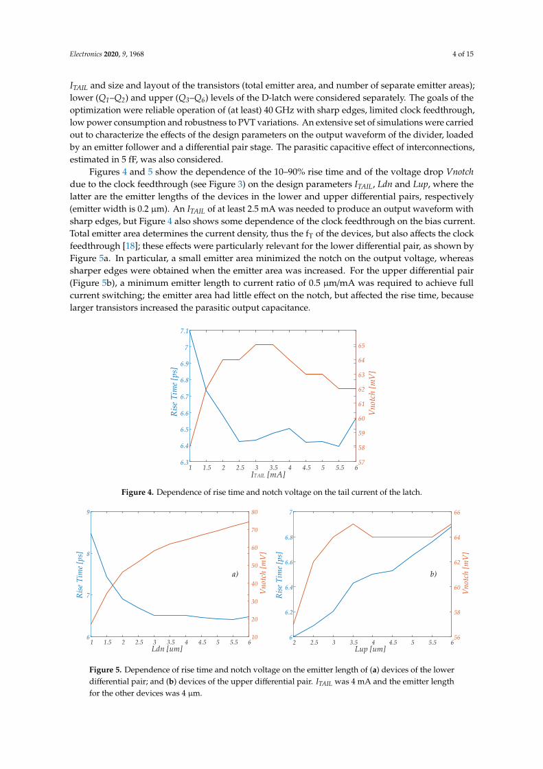
ITAIL and size and layout of the transistors (total emitter area, and number of separate emitter areas);lower (Q1–Q2) and upper (Q3–Q6) levels of the D-latch were considered separately. The goals of theoptimization were reliable operation of (at least) 40 GHz with sharp edges, limited clock feedthrough,low power consumption and robustness to PVT variations. An extensive set of simulations were carriedout to characterize the effects of the design parameters on the output waveform of the divider, loadedby an emitter follower and a differential pair stage. The parasitic capacitive effect of interconnections,estimated in 5 fF, was also considered.
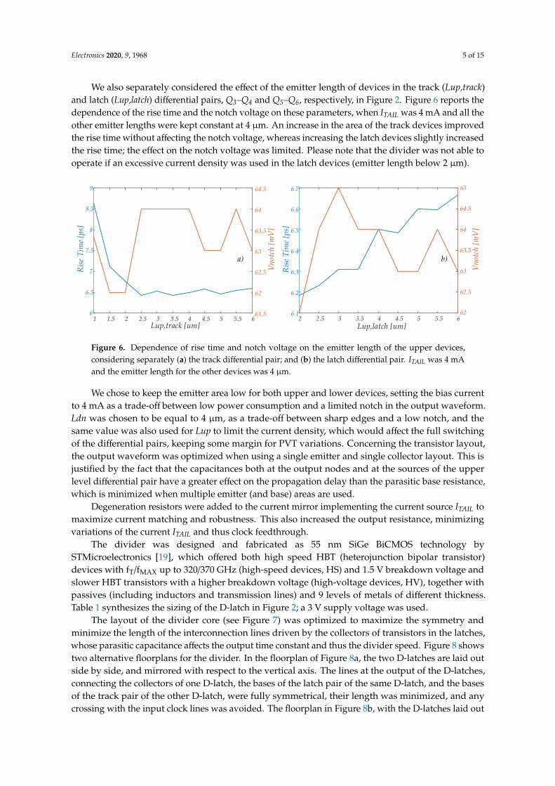
Figures 4 and 5 show the dependence of the 10–90% rise time and of the voltage drop Vnotchdue to the clock feedthrough (see Figure 3) on the design parameters ITAIL, Ldn and Lup, where thelatter are the emitter lengths of the devices in the lower and upper differential pairs, respectively(emitter width is 0.2 µm). An ITAIL of at least 2.5 mA was needed to produce an output waveform withsharp edges, but Figure 4 also shows some dependence of the clock feedthrough on the bias current.Total emitter area determines the current density, thus the fT of the devices, but also affects the clockfeedthrough [18]; these effects were particularly relevant for the lower differential pair, as shown byFigure 5a. In particular, a small emitter area minimized the notch on the output voltage, whereassharper edges were obtained when the emitter area was increased. For the upper differential pair(Figure 5b), a minimum emitter length to current ratio of 0.5 µm/mA was required to achieve fullcurrent switching; the emitter area had little effect on the notch, but affected the rise time, becauselarger transistors increased the parasitic output capacitance.
Electronics 2020, 9, x FOR PEER REVIEW 4 of 15
areas); lower (Q1–Q2) and upper (Q3–Q6) levels of the D-latch were considered separately. The goals of the optimization were reliable operation of (at least) 40 GHz with sharp edges, limited clock feedthrough, low power consumption and robustness to PVT variations. An extensive set of simulations were carried out to characterize the effects of the design parameters on the output waveform of the divider, loaded by an emitter follower and a differential pair stage. The parasitic capacitive effect of interconnections, estimated in 5 fF, was also considered.
Figures 4 and 5 show the dependence of the 10–90% rise time and of the voltage drop Vnotch due to the clock feedthrough (see Figure 3) on the design parameters ITAIL, Ldn and Lup, where the latter are the emitter lengths of the devices in the lower and upper differential pairs, respectively (emitter width is 0.2 μm). An ITAIL of at least 2.5 mA was needed to produce an output waveform with sharp edges, but Figure 4 also shows some dependence of the clock feedthrough on the bias current. Total emitter area determines the current density, thus the fT of the devices, but also affects the clock feedthrough [18]; these effects were particularly relevant for the lower differential pair, as shown by Figure 5a. In particular, a small emitter area minimized the notch on the output voltage, whereas sharper edges were obtained when the emitter area was increased. For the upper differential pair (Figure 5b), a minimum emitter length to current ratio of 0.5 μm/mA was required to achieve full current switching; the emitter area had little effect on the notch, but affected the rise time, because larger transistors increased the parasitic output capacitance.
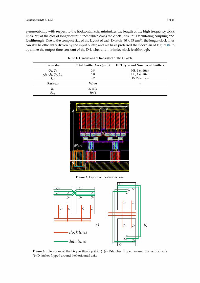
We also separately considered the effect of the emitter length of devices in the track (Lup,track) and latch (Lup,latch) differential pairs, Q3–Q4 and Q5–Q6, respectively, in Figure 2. Figure 6 reports the dependence of the rise time and the notch voltage on these parameters, when ITAIL was 4 mA and all the other emitter lengths were kept constant at 4 μm. An increase in the area of the track devices improved the rise time without affecting the notch voltage, whereas increasing the latch devices slightly increased the rise time; the effect on the notch voltage was limited. Please note that the divider was not able to operate if an excessive current density was used in the latch devices (emitter length below 2 μm).
Figure 4. Dependence of rise time and notch voltage on the tail current of the latch.
1 1.5 2 2.5 3 3.5 4 4.5 5 5.5 6ITAIL [mA]
6.3
6.4
6.5
6.6
6.7
6.8
6.9
7
7.1
Rise
Tim
e [ps
]
57
58
59
60
61
62
63
64
65
Vnot
ch [m
V]
Figure 4. Dependence of rise time and notch voltage on the tail current of the latch.Electronics 2020, 9, x FOR PEER REVIEW 5 of 15
Figure 5. Dependence of rise time and notch voltage on the emitter length of (a) devices of the lower differential pair; and (b) devices of the upper differential pair. ITAIL was 4 mA and the emitter length for the other devices was 4 μm.
Figure 6. Dependence of rise time and notch voltage on the emitter length of the upper devices, considering separately (a) the track differential pair; and (b) the latch differential pair. ITAIL was 4 mA and the emitter length for the other devices was 4 μm.
We chose to keep the emitter area low for both upper and lower devices, setting the bias current to 4 mA as a trade-off between low power consumption and a limited notch in the output waveform. Ldn was chosen to be equal to 4 μm, as a trade-off between sharp edges and a low notch, and the same value was also used for Lup to limit the current density, which would affect the full switching of the differential pairs, keeping some margin for PVT variations. Concerning the transistor layout, the output waveform was optimized when using a single emitter and single collector layout. This is justified by the fact that the capacitances both at the output nodes and at the sources of the upper level differential pair have a greater effect on the propagation delay than the parasitic base resistance, which is minimized when multiple emitter (and base) areas are used.
Degeneration resistors were added to the current mirror implementing the current source ITAIL to maximize current matching and robustness. This also increased the output resistance, minimizing variations of the current ITAIL and thus clock feedthrough.
The divider was designed and fabricated as 55 nm SiGe BiCMOS technology by STMicroelectronics [19], which offered both high speed HBT (heterojunction bipolar transistor) devices with fT/fMAX up to 320/370 GHz (high-speed devices, HS) and 1.5 V breakdown voltage and slower HBT transistors with a higher breakdown voltage (high-voltage devices, HV), together with passives (including inductors and transmission lines) and 9 levels of metals of different thickness. Table 1 synthesizes the sizing of the D-latch in Figure 2; a 3 V supply voltage was used.
1 1.5 2 2.5 3 3.5 4 4.5 5 5.5 6Ldn [um]
6
7
8
9
10
20
30
40
50
60
70
80
Vnot
ch [m
V]
Rise
Tim
e [ps
]
2 2.5 3 3.5 4 4.5 5 5.5 6Lup [um]
6
6.2
6.4
6.6
6.8
7
56
58
60
62
64
66
Vnot
ch [m
V]
Rise
Tim
e [ps
]
a) b)
Lup,track [um]
Vnot
ch [m
V]
Rise
Tim
e [ps
]
1 1.5 2 2.5 3 3.5 4 4.5 5 5.5 66
6.5
7
7.5
8
8.5
9
61.5
62
62.5
63
63.5
64
64.5
Lup,latch [um]
Vnot
ch [m
V]
Rise
Tim
e [ps
]
2 2.5 3 3.5 4 4.5 5 5.5 66.1
6.2
6.3
6.4
6.5
6.6
6.7
62
62.5
63
63.5
64
64.5
65
a) b)
Figure 5. Dependence of rise time and notch voltage on the emitter length of (a) devices of the lowerdifferential pair; and (b) devices of the upper differential pair. ITAIL was 4 mA and the emitter lengthfor the other devices was 4 µm.
Electronics 2020, 9, 1968 5 of 15
We also separately considered the effect of the emitter length of devices in the track (Lup,track)and latch (Lup,latch) differential pairs, Q3–Q4 and Q5–Q6, respectively, in Figure 2. Figure 6 reports thedependence of the rise time and the notch voltage on these parameters, when ITAIL was 4 mA and all theother emitter lengths were kept constant at 4 µm. An increase in the area of the track devices improvedthe rise time without affecting the notch voltage, whereas increasing the latch devices slightly increasedthe rise time; the effect on the notch voltage was limited. Please note that the divider was not able tooperate if an excessive current density was used in the latch devices (emitter length below 2 µm).
Electronics 2020, 9, x FOR PEER REVIEW 5 of 15
Figure 5. Dependence of rise time and notch voltage on the emitter length of (a) devices of the lower differential pair; and (b) devices of the upper differential pair. ITAIL was 4 mA and the emitter length for the other devices was 4 μm.
Figure 6. Dependence of rise time and notch voltage on the emitter length of the upper devices, considering separately (a) the track differential pair; and (b) the latch differential pair. ITAIL was 4 mA and the emitter length for the other devices was 4 μm.
We chose to keep the emitter area low for both upper and lower devices, setting the bias current to 4 mA as a trade-off between low power consumption and a limited notch in the output waveform. Ldn was chosen to be equal to 4 μm, as a trade-off between sharp edges and a low notch, and the same value was also used for Lup to limit the current density, which would affect the full switching of the differential pairs, keeping some margin for PVT variations. Concerning the transistor layout, the output waveform was optimized when using a single emitter and single collector layout. This is justified by the fact that the capacitances both at the output nodes and at the sources of the upper level differential pair have a greater effect on the propagation delay than the parasitic base resistance, which is minimized when multiple emitter (and base) areas are used.
Degeneration resistors were added to the current mirror implementing the current source ITAIL to maximize current matching and robustness. This also increased the output resistance, minimizing variations of the current ITAIL and thus clock feedthrough.
The divider was designed and fabricated as 55 nm SiGe BiCMOS technology by STMicroelectronics [19], which offered both high speed HBT (heterojunction bipolar transistor) devices with fT/fMAX up to 320/370 GHz (high-speed devices, HS) and 1.5 V breakdown voltage and slower HBT transistors with a higher breakdown voltage (high-voltage devices, HV), together with passives (including inductors and transmission lines) and 9 levels of metals of different thickness. Table 1 synthesizes the sizing of the D-latch in Figure 2; a 3 V supply voltage was used.
1 1.5 2 2.5 3 3.5 4 4.5 5 5.5 6Ldn [um]
6
7
8
9
10
20
30
40
50
60
70
80
Vnot
ch [m
V]
Rise
Tim
e [ps
]
2 2.5 3 3.5 4 4.5 5 5.5 6Lup [um]
6
6.2
6.4
6.6
6.8
7
56
58
60
62
64
66
Vnot
ch [m
V]
Rise
Tim
e [ps
]
a) b)
Lup,track [um]
Vnot
ch [m
V]
Rise
Tim
e [ps
]
1 1.5 2 2.5 3 3.5 4 4.5 5 5.5 66
6.5
7
7.5
8
8.5
9
61.5
62
62.5
63
63.5
64
64.5
Lup,latch [um]
Vnot
ch [m
V]
Rise
Tim
e [ps
]
2 2.5 3 3.5 4 4.5 5 5.5 66.1
6.2
6.3
6.4
6.5
6.6
6.7
62
62.5
63
63.5
64
64.5
65
a) b)
Figure 6. Dependence of rise time and notch voltage on the emitter length of the upper devices,considering separately (a) the track differential pair; and (b) the latch differential pair. ITAIL was 4 mAand the emitter length for the other devices was 4 µm.
We chose to keep the emitter area low for both upper and lower devices, setting the bias currentto 4 mA as a trade-off between low power consumption and a limited notch in the output waveform.Ldn was chosen to be equal to 4 µm, as a trade-off between sharp edges and a low notch, and thesame value was also used for Lup to limit the current density, which would affect the full switchingof the differential pairs, keeping some margin for PVT variations. Concerning the transistor layout,the output waveform was optimized when using a single emitter and single collector layout. This isjustified by the fact that the capacitances both at the output nodes and at the sources of the upperlevel differential pair have a greater effect on the propagation delay than the parasitic base resistance,which is minimized when multiple emitter (and base) areas are used.
Degeneration resistors were added to the current mirror implementing the current source ITAIL tomaximize current matching and robustness. This also increased the output resistance, minimizingvariations of the current ITAIL and thus clock feedthrough.
The divider was designed and fabricated as 55 nm SiGe BiCMOS technology bySTMicroelectronics [19], which offered both high speed HBT (heterojunction bipolar transistor)devices with fT/fMAX up to 320/370 GHz (high-speed devices, HS) and 1.5 V breakdown voltage andslower HBT transistors with a higher breakdown voltage (high-voltage devices, HV), together withpassives (including inductors and transmission lines) and 9 levels of metals of different thickness.Table 1 synthesizes the sizing of the D-latch in Figure 2; a 3 V supply voltage was used.
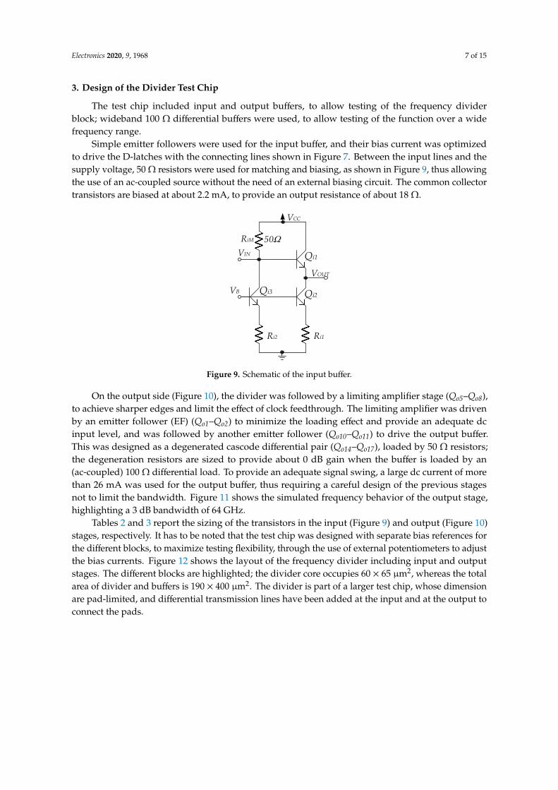
The layout of the divider core (see Figure 7) was optimized to maximize the symmetry andminimize the length of the interconnection lines driven by the collectors of transistors in the latches,whose parasitic capacitance affects the output time constant and thus the divider speed. Figure 8 showstwo alternative floorplans for the divider. In the floorplan of Figure 8a, the two D-latches are laid outside by side, and mirrored with respect to the vertical axis. The lines at the output of the D-latches,connecting the collectors of one D-latch, the bases of the latch pair of the same D-latch, and the basesof the track pair of the other D-latch, were fully symmetrical, their length was minimized, and anycrossing with the input clock lines was avoided. The floorplan in Figure 8b, with the D-latches laid out
Electronics 2020, 9, 1968 6 of 15
symmetrically with respect to the horizontal axis, minimizes the length of the high frequency clocklines, but at the cost of longer output lines which cross the clock lines, thus facilitating coupling andfeedthrough. Due to the compact size of the layout of each D-latch (30 × 65 µm2), the longer clock linescan still be efficiently driven by the input buffer, and we have preferred the floorplan of Figure 8a tooptimize the output time constant of the D-latches and minimize clock feedthrough.
Table 1. Dimensions of transistors of the D-latch.
Transistor Total Emitter Area (µm2) HBT Type and Number of Emitters
Q1, Q2 0.8 HS, 1 emitterQ3, Q4, Q5, Q6 0.8 HS, 1 emitter
Q7 3.2 HS, 2 emitters
Resistor Value -
RC 37.5 Ω -Rdeg 50 Ω -
Electronics 2020, 9, x FOR PEER REVIEW 6 of 15
Table 1. Dimensions of transistors of the D-latch.
Transistor Total Emitter
Area (μm2) HBT Type and
Number of Emitters Q1, Q2 0.8 HS, 1 emitter
Q3, Q4, Q5, Q6 0.8 HS, 1 emitter Q7 3.2 HS, 2 emitters
Resistor Value - RC 37.5 Ω - Rdeg 50 Ω -
The layout of the divider core (see Figure 7) was optimized to maximize the symmetry and minimize the length of the interconnection lines driven by the collectors of transistors in the latches, whose parasitic capacitance affects the output time constant and thus the divider speed. Figure 8 shows two alternative floorplans for the divider. In the floorplan of Figure 8a, the two D-latches are laid out side by side, and mirrored with respect to the vertical axis. The lines at the output of the D-latches, connecting the collectors of one D-latch, the bases of the latch pair of the same D-latch, and the bases of the track pair of the other D-latch, were fully symmetrical, their length was minimized, and any crossing with the input clock lines was avoided. The floorplan in Figure 8b, with the D-latches laid out symmetrically with respect to the horizontal axis, minimizes the length of the high frequency clock lines, but at the cost of longer output lines which cross the clock lines, thus facilitating coupling and feedthrough. Due to the compact size of the layout of each D-latch (30 × 65 μm2), the longer clock lines can still be efficiently driven by the input buffer, and we have preferred the floorplan of Figure 8a to optimize the output time constant of the D-latches and minimize clock feedthrough.
Figure 7. Layout of the divider core.
65um
60um
Figure 7. Layout of the divider core.Electronics 2020, 9, x FOR PEER REVIEW 7 of 15
Figure 8. Floorplan of the D-type flip-flop (DFF): (a) D-latches flipped around the vertical axis; (b) D-latches flipped around the horizontal axis.
3. Design of the Divider Test Chip
The test chip included input and output buffers, to allow testing of the frequency divider block; wideband 100 Ω differential buffers were used, to allow testing of the function over a wide frequency range.
Simple emitter followers were used for the input buffer, and their bias current was optimized to drive the D-latches with the connecting lines shown in Figure 7. Between the input lines and the supply voltage, 50 Ω resistors were used for matching and biasing, as shown in Figure 9, thus allowing the use of an ac-coupled source without the need of an external biasing circuit. The common collector transistors are biased at about 2.2 mA, to provide an output resistance of about 18 Ω.
On the output side (Figure 10), the divider was followed by a limiting amplifier stage (Qo5–Qo8), to achieve sharper edges and limit the effect of clock feedthrough. The limiting amplifier was driven by an emitter follower (EF) (Qo1–Qo2) to minimize the loading effect and provide an adequate dc input level, and was followed by another emitter follower (Qo10–Qo11) to drive the output buffer. This was designed as a degenerated cascode differential pair (Qo14–Qo17), loaded by 50 Ω resistors; the degeneration resistors are sized to provide about 0 dB gain when the buffer is loaded by an (ac-coupled) 100 Ω differential load. To provide an adequate signal swing, a large dc current of more than 26 mA was used for the output buffer, thus requiring a careful design of the previous stages not to limit the bandwidth. Figure 11 shows the simulated frequency behavior of the output stage, highlighting a 3 dB bandwidth of 64 GHz.
Figure 9. Schematic of the input buffer.
a) b)clock lines
data lines
C+
C+
C+
C+
C-
C-
Q+ Q+Q+
Q+
Q- Q-Q-
D+
D-
D+D+
D-
D+
D- D-
Q-
C-
C-
RiM 50Ω
VCC
Qi1
Qi2Qi3
Ri1Ri2
VB
VIN
VOUT
Figure 8. Floorplan of the D-type flip-flop (DFF): (a) D-latches flipped around the vertical axis;(b) D-latches flipped around the horizontal axis.
Electronics 2020, 9, 1968 7 of 15
3. Design of the Divider Test Chip
The test chip included input and output buffers, to allow testing of the frequency dividerblock; wideband 100 Ω differential buffers were used, to allow testing of the function over a widefrequency range.
Simple emitter followers were used for the input buffer, and their bias current was optimizedto drive the D-latches with the connecting lines shown in Figure 7. Between the input lines and thesupply voltage, 50 Ω resistors were used for matching and biasing, as shown in Figure 9, thus allowingthe use of an ac-coupled source without the need of an external biasing circuit. The common collectortransistors are biased at about 2.2 mA, to provide an output resistance of about 18 Ω.
Electronics 2020, 9, x FOR PEER REVIEW 7 of 15
Figure 8. Floorplan of the D-type flip-flop (DFF): (a) D-latches flipped around the vertical axis; (b) D-latches flipped around the horizontal axis.
3. Design of the Divider Test Chip
The test chip included input and output buffers, to allow testing of the frequency divider block; wideband 100 Ω differential buffers were used, to allow testing of the function over a wide frequency range.
Simple emitter followers were used for the input buffer, and their bias current was optimized to drive the D-latches with the connecting lines shown in Figure 7. Between the input lines and the supply voltage, 50 Ω resistors were used for matching and biasing, as shown in Figure 9, thus allowing the use of an ac-coupled source without the need of an external biasing circuit. The common collector transistors are biased at about 2.2 mA, to provide an output resistance of about 18 Ω.
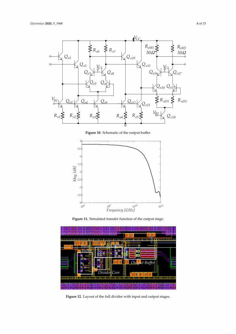
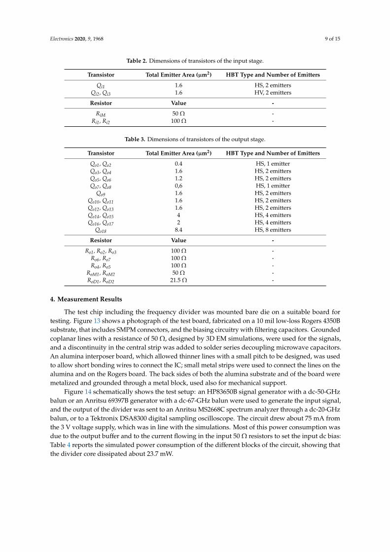
On the output side (Figure 10), the divider was followed by a limiting amplifier stage (Qo5–Qo8), to achieve sharper edges and limit the effect of clock feedthrough. The limiting amplifier was driven by an emitter follower (EF) (Qo1–Qo2) to minimize the loading effect and provide an adequate dc input level, and was followed by another emitter follower (Qo10–Qo11) to drive the output buffer. This was designed as a degenerated cascode differential pair (Qo14–Qo17), loaded by 50 Ω resistors; the degeneration resistors are sized to provide about 0 dB gain when the buffer is loaded by an (ac-coupled) 100 Ω differential load. To provide an adequate signal swing, a large dc current of more than 26 mA was used for the output buffer, thus requiring a careful design of the previous stages not to limit the bandwidth. Figure 11 shows the simulated frequency behavior of the output stage, highlighting a 3 dB bandwidth of 64 GHz.
Figure 9. Schematic of the input buffer.
a) b)clock lines
data lines
C+
C+
C+
C+
C-
C-
Q+ Q+Q+
Q+
Q- Q-Q-
D+
D-
D+D+
D-
D+
D- D-
Q-
C-
C-
RiM 50Ω
VCC
Qi1
Qi2Qi3
Ri1Ri2
VB
VIN
VOUT
Figure 9. Schematic of the input buffer.
On the output side (Figure 10), the divider was followed by a limiting amplifier stage (Qo5–Qo8),to achieve sharper edges and limit the effect of clock feedthrough. The limiting amplifier was drivenby an emitter follower (EF) (Qo1–Qo2) to minimize the loading effect and provide an adequate dcinput level, and was followed by another emitter follower (Qo10–Qo11) to drive the output buffer.This was designed as a degenerated cascode differential pair (Qo14–Qo17), loaded by 50 Ω resistors;the degeneration resistors are sized to provide about 0 dB gain when the buffer is loaded by an(ac-coupled) 100 Ω differential load. To provide an adequate signal swing, a large dc current of morethan 26 mA was used for the output buffer, thus requiring a careful design of the previous stagesnot to limit the bandwidth. Figure 11 shows the simulated frequency behavior of the output stage,highlighting a 3 dB bandwidth of 64 GHz.
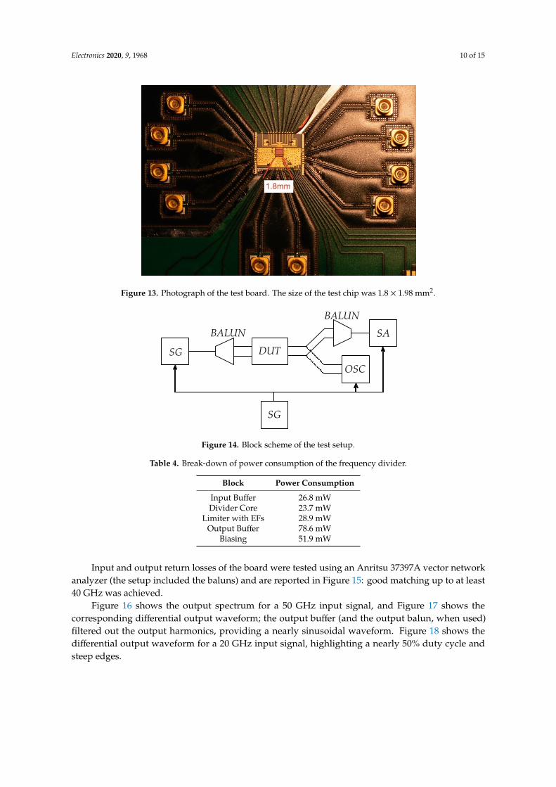
Tables 2 and 3 report the sizing of the transistors in the input (Figure 9) and output (Figure 10)stages, respectively. It has to be noted that the test chip was designed with separate bias references forthe different blocks, to maximize testing flexibility, through the use of external potentiometers to adjustthe bias currents. Figure 12 shows the layout of the frequency divider including input and outputstages. The different blocks are highlighted; the divider core occupies 60 × 65 µm2, whereas the totalarea of divider and buffers is 190 × 400 µm2. The divider is part of a larger test chip, whose dimensionare pad-limited, and differential transmission lines have been added at the input and at the output toconnect the pads.
Electronics 2020, 9, 1968 8 of 15Electronics 2020, 9, x FOR PEER REVIEW 8 of 15
Figure 10. Schematic of the output buffer.
Tables 2 and 3 report the sizing of the transistors in the input (Figure 9) and output (Figure 10) stages, respectively. It has to be noted that the test chip was designed with separate bias references for the different blocks, to maximize testing flexibility, through the use of external potentiometers to adjust the bias currents. Figure 12 shows the layout of the frequency divider including input and output stages. The different blocks are highlighted; the divider core occupies 60 × 65 μm2, whereas the total area of divider and buffers is 190 × 400 μm2. The divider is part of a larger test chip, whose dimension are pad-limited, and differential transmission lines have been added at the input and at the output to connect the pads.
Figure 11. Simulated transfer function of the output stage.
VCC
VB1 RoD2RoD1
RoM2RoM1
Ro5Ro4Ro3Ro2Ro1 Qo18
Qo17Qo16
Qo15Qo14
Qo11
Qo10
Qo8Qo7
Qo6Qo5
Qo12 Qo13Qo9Qo4
Qo1
Qo2 VC1 VC2
VB2
50Ω50Ω
Qo3
Ro6 Ro7
Frequency [GHz]
Mag
[dB]
108 109 1010 1011-4
-3.5
-3
-2.5
-2
-1.5
-1
-0.5
0
Figure 10. Schematic of the output buffer.
Electronics 2020, 9, x FOR PEER REVIEW 8 of 15
Figure 10. Schematic of the output buffer.
Tables 2 and 3 report the sizing of the transistors in the input (Figure 9) and output (Figure 10) stages, respectively. It has to be noted that the test chip was designed with separate bias references for the different blocks, to maximize testing flexibility, through the use of external potentiometers to adjust the bias currents. Figure 12 shows the layout of the frequency divider including input and output stages. The different blocks are highlighted; the divider core occupies 60 × 65 μm2, whereas the total area of divider and buffers is 190 × 400 μm2. The divider is part of a larger test chip, whose dimension are pad-limited, and differential transmission lines have been added at the input and at the output to connect the pads.
Figure 11. Simulated transfer function of the output stage.
VCC
VB1 RoD2RoD1
RoM2RoM1
Ro5Ro4Ro3Ro2Ro1 Qo18
Qo17Qo16
Qo15Qo14
Qo11
Qo10
Qo8Qo7
Qo6Qo5
Qo12 Qo13Qo9Qo4
Qo1
Qo2 VC1 VC2
VB2
50Ω50Ω
Qo3
Ro6 Ro7
Frequency [GHz]
Mag
[dB]
108 109 1010 1011-4
-3.5
-3
-2.5
-2
-1.5
-1
-0.5
0
Figure 11. Simulated transfer function of the output stage.Electronics 2020, 9, x FOR PEER REVIEW 10 of 15
Figure 12. Layout of the full divider with input and output stages.
Figure 13. Photograph of the test board. The size of the test chip was 1.8 × 1.98 mm2.
Figure 14. Block scheme of the test setup.
InputBuffer
EF & Limiter
Output Buffer
Divider Core
SG
SG
DUT
SA
OSC
BALUNBALUN
Figure 12. Layout of the full divider with input and output stages.
Electronics 2020, 9, 1968 9 of 15
Table 2. Dimensions of transistors of the input stage.
Transistor Total Emitter Area (µm2) HBT Type and Number of Emitters
Qi1 1.6 HS, 2 emittersQi2, Qi3 1.6 HV, 2 emitters
Resistor Value -
RiM 50 Ω -Ri1, Ri2 100 Ω -
Table 3. Dimensions of transistors of the output stage.
Transistor Total Emitter Area (µm2) HBT Type and Number of Emitters
Qo1, Qo2 0.4 HS, 1 emitterQo3, Qo4 1.6 HS, 2 emittersQo5, Qo6 1.2 HS, 2 emittersQo7, Qo8 0,6 HS, 1 emitter
Qo9 1.6 HS, 2 emittersQo10, Qo11 1.6 HS, 2 emittersQo12, Qo13 1.6 HS, 2 emittersQo14, Qo15 4 HS, 4 emittersQo16, Qo17 2 HS, 4 emitters
Qo18 8.4 HS, 8 emitters
Resistor Value -
Ro1, Ro2, Ro3 100 Ω -Ro6, Ro7 100 Ω -Ro4, Ro5 100 Ω -
RoM1, RoM2 50 Ω -RoD1, RoD2 21.5 Ω -
4. Measurement Results
The test chip including the frequency divider was mounted bare die on a suitable board fortesting. Figure 13 shows a photograph of the test board, fabricated on a 10 mil low-loss Rogers 4350Bsubstrate, that includes SMPM connectors, and the biasing circuitry with filtering capacitors. Groundedcoplanar lines with a resistance of 50 Ω, designed by 3D EM simulations, were used for the signals,and a discontinuity in the central strip was added to solder series decoupling microwave capacitors.An alumina interposer board, which allowed thinner lines with a small pitch to be designed, was usedto allow short bonding wires to connect the IC; small metal strips were used to connect the lines on thealumina and on the Rogers board. The back sides of both the alumina substrate and of the board weremetalized and grounded through a metal block, used also for mechanical support.
Figure 14 schematically shows the test setup: an HP83650B signal generator with a dc-50-GHzbalun or an Anritsu 69397B generator with a dc-67-GHz balun were used to generate the input signal,and the output of the divider was sent to an Anritsu MS2668C spectrum analyzer through a dc-20-GHzbalun, or to a Tektronix DSA8300 digital sampling oscilloscope. The circuit drew about 75 mA fromthe 3 V voltage supply, which was in line with the simulations. Most of this power consumption wasdue to the output buffer and to the current flowing in the input 50 Ω resistors to set the input dc bias:Table 4 reports the simulated power consumption of the different blocks of the circuit, showing thatthe divider core dissipated about 23.7 mW.
Electronics 2020, 9, 1968 10 of 15
Electronics 2020, 9, x FOR PEER REVIEW 10 of 15
Figure 12. Layout of the full divider with input and output stages.
Figure 13. Photograph of the test board. The size of the test chip was 1.8 × 1.98 mm2.
Figure 14. Block scheme of the test setup.
InputBuffer
EF & Limiter
Output Buffer
Divider Core
SG
SG
DUT
SA
OSC
BALUNBALUN
Figure 13. Photograph of the test board. The size of the test chip was 1.8 × 1.98 mm2.
Electronics 2020, 9, x FOR PEER REVIEW 10 of 15
Figure 12. Layout of the full divider with input and output stages.
Figure 13. Photograph of the test board. The size of the test chip was 1.8 × 1.98 mm2.
Figure 14. Block scheme of the test setup.
InputBuffer
EF & Limiter
Output Buffer
Divider Core
SG
SG
DUT
SA
OSC
BALUNBALUN
Figure 14. Block scheme of the test setup.
Table 4. Break-down of power consumption of the frequency divider.
Block Power Consumption
Input Buffer 26.8 mWDivider Core 23.7 mW
Limiter with EFs 28.9 mWOutput Buffer 78.6 mW
Biasing 51.9 mW
Input and output return losses of the board were tested using an Anritsu 37397A vector networkanalyzer (the setup included the baluns) and are reported in Figure 15: good matching up to at least40 GHz was achieved.
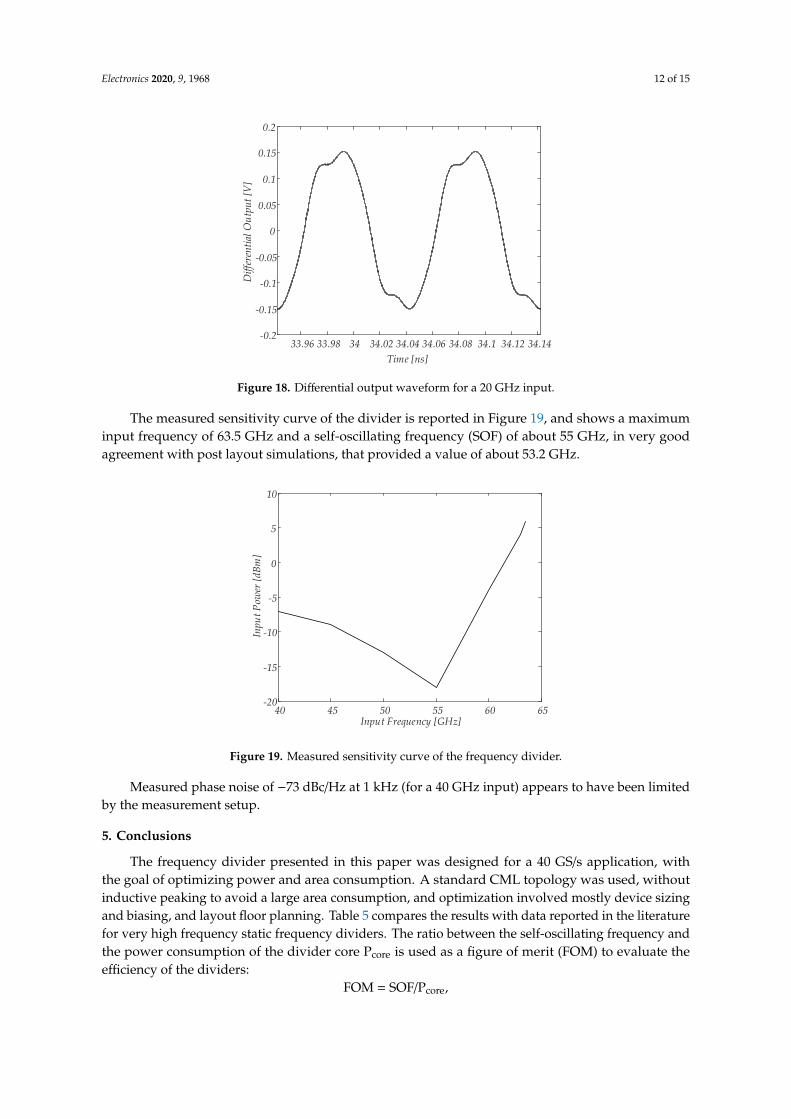
Figure 16 shows the output spectrum for a 50 GHz input signal, and Figure 17 shows thecorresponding differential output waveform; the output buffer (and the output balun, when used)filtered out the output harmonics, providing a nearly sinusoidal waveform. Figure 18 shows thedifferential output waveform for a 20 GHz input signal, highlighting a nearly 50% duty cycle andsteep edges.
Electronics 2020, 9, 1968 11 of 15
Electronics 2020, 9, x FOR PEER REVIEW 11 of 15
Table 4. Break-down of power consumption of the frequency divider.
Block Power Consumption Input Buffer 26.8 mW Divider Core 23.7 mW
Limiter with EFs 28.9 mW Output Buffer 78.6 mW
Biasing 51.9 mW
Input and output return losses of the board were tested using an Anritsu 37397A vector network analyzer (the setup included the baluns) and are reported in Figure 15: good matching up to at least 40 GHz was achieved.
Figure 16 shows the output spectrum for a 50 GHz input signal, and Figure 17 shows the corresponding differential output waveform; the output buffer (and the output balun, when used) filtered out the output harmonics, providing a nearly sinusoidal waveform. Figure 18 shows the differential output waveform for a 20 GHz input signal, highlighting a nearly 50% duty cycle and steep edges.
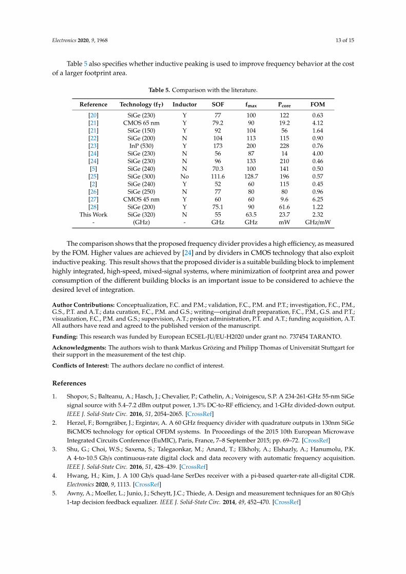
The measured sensitivity curve of the divider is reported in Figure 19, and shows a maximum input frequency of 63.5 GHz and a self-oscillating frequency (SOF) of about 55 GHz, in very good agreement with post layout simulations, that provided a value of about 53.2 GHz.
Measured phase noise of −73 dBc/Hz at 1 kHz (for a 40 GHz input) appears to have been limited by the measurement setup.
Figure 15. Measured input and output return losses.
S11
[dB]
0 20 40 60Frequency [GHz]
-45
-40
-35
-30
-25
-20
-15
-10
-5
0 20 40 60Frequency [GHz]
-45
-40
-35
-30
-25
-20
-15
-10
-5
S22
[dB]
Figure 15. Measured input and output return losses.
Electronics 2020, 9, x FOR PEER REVIEW 11 of 15
Table 4. Break-down of power consumption of the frequency divider.
Block Power Consumption Input Buffer 26.8 mW Divider Core 23.7 mW
Limiter with EFs 28.9 mW Output Buffer 78.6 mW
Biasing 51.9 mW
Input and output return losses of the board were tested using an Anritsu 37397A vector network analyzer (the setup included the baluns) and are reported in Figure 15: good matching up to at least 40 GHz was achieved.
Figure 16 shows the output spectrum for a 50 GHz input signal, and Figure 17 shows the corresponding differential output waveform; the output buffer (and the output balun, when used) filtered out the output harmonics, providing a nearly sinusoidal waveform. Figure 18 shows the differential output waveform for a 20 GHz input signal, highlighting a nearly 50% duty cycle and steep edges.
The measured sensitivity curve of the divider is reported in Figure 19, and shows a maximum input frequency of 63.5 GHz and a self-oscillating frequency (SOF) of about 55 GHz, in very good agreement with post layout simulations, that provided a value of about 53.2 GHz.
Measured phase noise of −73 dBc/Hz at 1 kHz (for a 40 GHz input) appears to have been limited by the measurement setup.
Figure 15. Measured input and output return losses.
S11
[dB]
0 20 40 60Frequency [GHz]
-45
-40
-35
-30
-25
-20
-15
-10
-5
0 20 40 60Frequency [GHz]
-45
-40
-35
-30
-25
-20
-15
-10
-5
S22
[dB]
Figure 16. Output spectrum for a 50 GHz input.
Electronics 2020, 9, x FOR PEER REVIEW 12 of 15
Figure 16. Output spectrum for a 50 GHz input.
Figure 17. Differential output waveform for a 50 GHz input.
Figure 18. Differential output waveform for a 20 GHz input.
Figure 19. Measured sensitivity curve of the frequency divider.
33.96 33.98 34 34.02 34.04 34.06 34.08 34.1 34.12 34.14Time [ns]
-0.15
-0.1
-0.05
0
0.05
0.1
Diff
eren
tial O
utpu
t [V]
33.96 33.98 34 34.02 34.04 34.06 34.08 34.1 34.12 34.14Time [ns]
-0.2
-0.15
-0.1
-0.05
0
0.05
0.1
0.15
0.2
Diff
eren
tial O
utpu
t [V]
40 45 50 55 60 65Input Frequency [GHz]
-20
-15
-10
-5
0
5
10
Inpu
t Pow
er [d
Bm]
Figure 17. Differential output waveform for a 50 GHz input.
Electronics 2020, 9, 1968 12 of 15
Electronics 2020, 9, x FOR PEER REVIEW 12 of 15
Figure 16. Output spectrum for a 50 GHz input.
Figure 17. Differential output waveform for a 50 GHz input.
Figure 18. Differential output waveform for a 20 GHz input.
Figure 19. Measured sensitivity curve of the frequency divider.
33.96 33.98 34 34.02 34.04 34.06 34.08 34.1 34.12 34.14Time [ns]
-0.15
-0.1
-0.05
0
0.05
0.1
Diff
eren
tial O
utpu
t [V]
33.96 33.98 34 34.02 34.04 34.06 34.08 34.1 34.12 34.14Time [ns]
-0.2
-0.15
-0.1
-0.05
0
0.05
0.1
0.15
0.2
Diff
eren
tial O
utpu
t [V]
40 45 50 55 60 65Input Frequency [GHz]
-20
-15
-10
-5
0
5
10
Inpu
t Pow
er [d
Bm]
Figure 18. Differential output waveform for a 20 GHz input.
The measured sensitivity curve of the divider is reported in Figure 19, and shows a maximuminput frequency of 63.5 GHz and a self-oscillating frequency (SOF) of about 55 GHz, in very goodagreement with post layout simulations, that provided a value of about 53.2 GHz.
Electronics 2020, 9, x FOR PEER REVIEW 12 of 15
Figure 16. Output spectrum for a 50 GHz input.
Figure 17. Differential output waveform for a 50 GHz input.
Figure 18. Differential output waveform for a 20 GHz input.
Figure 19. Measured sensitivity curve of the frequency divider.
33.96 33.98 34 34.02 34.04 34.06 34.08 34.1 34.12 34.14Time [ns]
-0.15
-0.1
-0.05
0
0.05
0.1
Diff
eren
tial O
utpu
t [V]
33.96 33.98 34 34.02 34.04 34.06 34.08 34.1 34.12 34.14Time [ns]
-0.2
-0.15
-0.1
-0.05
0
0.05
0.1
0.15
0.2
Diff
eren
tial O
utpu
t [V]
40 45 50 55 60 65Input Frequency [GHz]
-20
-15
-10
-5
0
5
10
Inpu
t Pow
er [d
Bm]
Figure 19. Measured sensitivity curve of the frequency divider.
Measured phase noise of −73 dBc/Hz at 1 kHz (for a 40 GHz input) appears to have been limitedby the measurement setup.
5. Conclusions
The frequency divider presented in this paper was designed for a 40 GS/s application, withthe goal of optimizing power and area consumption. A standard CML topology was used, withoutinductive peaking to avoid a large area consumption, and optimization involved mostly device sizingand biasing, and layout floor planning. Table 5 compares the results with data reported in the literaturefor very high frequency static frequency dividers. The ratio between the self-oscillating frequency andthe power consumption of the divider core Pcore is used as a figure of merit (FOM) to evaluate theefficiency of the dividers:
FOM = SOF/Pcore,
Electronics 2020, 9, 1968 13 of 15
Table 5 also specifies whether inductive peaking is used to improve frequency behavior at the costof a larger footprint area.
Table 5. Comparison with the literature.
Reference Technology (fT) Inductor SOF fmax Pcore FOM
[20] SiGe (230) Y 77 100 122 0.63[21] CMOS 65 nm Y 79.2 90 19.2 4.12[21] SiGe (150) Y 92 104 56 1.64[22] SiGe (200) N 104 113 115 0.90[23] InP (530) Y 173 200 228 0.76[24] SiGe (230) N 56 87 14 4.00[24] SiGe (230) N 96 133 210 0.46[5] SiGe (240) N 70.3 100 141 0.50
[25] SiGe (300) No 111.6 128.7 196 0.57[2] SiGe (240) Y 52 60 115 0.45
[26] SiGe (250) N 77 80 80 0.96[27] CMOS 45 nm Y 60 60 9.6 6.25[28] SiGe (200) Y 75.1 90 61.6 1.22
This Work SiGe (320) N 55 63.5 23.7 2.32- (GHz) - GHz GHz mW GHz/mW
The comparison shows that the proposed frequency divider provides a high efficiency, as measuredby the FOM. Higher values are achieved by [24] and by dividers in CMOS technology that also exploitinductive peaking. This result shows that the proposed divider is a suitable building block to implementhighly integrated, high-speed, mixed-signal systems, where minimization of footprint area and powerconsumption of the different building blocks is an important issue to be considered to achieve thedesired level of integration.
Author Contributions: Conceptualization, F.C. and P.M.; validation, F.C., P.M. and P.T.; investigation, F.C., P.M.,G.S., P.T. and A.T.; data curation, F.C., P.M. and G.S.; writing—original draft preparation, F.C., P.M., G.S. and P.T.;visualization, F.C., P.M. and G.S.; supervision, A.T.; project administration, P.T. and A.T.; funding acquisition, A.T.All authors have read and agreed to the published version of the manuscript.
Funding: This research was funded by European ECSEL-JU/EU-H2020 under grant no. 737454 TARANTO.
Acknowledgments: The authors wish to thank Markus Grözing and Philipp Thomas of Universität Stuttgart fortheir support in the measurement of the test chip.
Conflicts of Interest: The authors declare no conflict of interest.
References
1. Shopov, S.; Balteanu, A.; Hasch, J.; Chevalier, P.; Cathelin, A.; Voinigescu, S.P. A 234-261-GHz 55-nm SiGesignal source with 5.4–7.2 dBm output power, 1.3% DC-to-RF efficiency, and 1-GHz divided-down output.IEEE J. Solid-State Circ. 2016, 51, 2054–2065. [CrossRef]
2. Herzel, F.; Borngräber, J.; Ergintav, A. A 60 GHz frequency divider with quadrature outputs in 130nm SiGeBiCMOS technology for optical OFDM systems. In Proceedings of the 2015 10th European MicrowaveIntegrated Circuits Conference (EuMIC), Paris, France, 7–8 September 2015; pp. 69–72. [CrossRef]
3. Shu, G.; Choi, W.S.; Saxena, S.; Talegaonkar, M.; Anand, T.; Elkholy, A.; Elshazly, A.; Hanumolu, P.K.A 4-to-10.5 Gb/s continuous-rate digital clock and data recovery with automatic frequency acquisition.IEEE J. Solid-State Circ. 2016, 51, 428–439. [CrossRef]
4. Hwang, H.; Kim, J. A 100 Gb/s quad-lane SerDes receiver with a pi-based quarter-rate all-digital CDR.Electronics 2020, 9, 1113. [CrossRef]
5. Awny, A.; Moeller, L.; Junio, J.; Scheytt, J.C.; Thiede, A. Design and measurement techniques for an 80 Gb/s1-tap decision feedback equalizer. IEEE J. Solid-State Circ. 2014, 49, 452–470. [CrossRef]
Electronics 2020, 9, 1968 14 of 15
6. Kull, L.; Luu, D.; Menolfi, C.; Brändli, M.; Francese, P.A.; Morf, T.; Kossel, M.; Cevrero, A.; Ozkaya, I.; Toifl, T.A 24-72-GS/s 8-b time-interleaved SAR ADC with 2.0-3.3-pJ/conversion and >30 dB SNDR at Nyquist in14-nm CMOS FinFET. IEEE J. Solid-State Circ. 2018, 53, 3508–3516. [CrossRef]
7. Grahn, J.V.; Fosshaug, H.; Jargelius, M.; Jönsson, P.; Linder, M.; Malm, B.G.; Mohadjeri, B.; Pejnefors, J.;Radamson, H.H.; Sandén, M.; et al. A low-complexity 62-GHz fT SiGe heterojunction bipolar transistorprocess using differential epitaxy and in situ phosphorus-doped poly-Si emitter at very low thermal budget.Solid-State Electron. 2000, 44, 549–554. [CrossRef]
8. Rücker, H.; Heinemann, B. High-performance SiGe HBTs for next generation BiCMOS technology. Semicond.Sci. Technol. 2018, 33, 114003. [CrossRef]
9. Zirath, H.; Carpenter, S.; He, Z.; Vassilev, V.; Bao, M. D-band MMIC design for high datarate wireless andwire-bound communication based on state-of-the-art InP DHBT and SiGe BiCMOS processes. In Proceedingsof the 2018 Asia-Pacific Microwave Conference (APMC), Kyoto, Japan, 6–9 November 2018. [CrossRef]
10. Voinigescu, S.P.; Shopov, S.; Hoffman, J.; Vasiliakopoulos, K. Analog and mixed-signal millimeter-waveSiGe BiCMOS circuits: State of the art and future scaling. In Proceedings of the 2016 IEEE CompoundSemiconductor Integrated Circuit Symposium (CSICS), Austin, TX, USA, 23–26 October 2016. [CrossRef]
11. Dyskin, A.; Kallfass, I. Amalytical approach for SiGe HBT static frequency divider design for millimeter-wavefrequency operation. IEEE Trans. Microw. Theory Techn. 2018, 66, 1411–1417. [CrossRef]
12. Seo, M.; Urteaga, M.; Young, A.; Rodwell, M. A 305–330+ GHz 2:1 dynamic frequency divider using InPHBTs. IEEE Microw. Wirel. Compon. Lett. 2010, 20, 468–470. [CrossRef]
13. Lin, Y.H.; Wang, H. A 35.7–64.2 GHz low power Miller divider with weak inversion mixer in 65 nm CMOS.IEEE Microw. Wireless Compon. Lett. 2016, 26, 948–950. [CrossRef]
14. Lin, B.-Y.; Liu, S.-I. Analysis and design of D-band injection-locked frequency dividers. IEEE J. Solid-StateCirc. 2011, 46, 1250–1264. [CrossRef]
15. Ali, U.; Bober, M.; Thiede, A.; Wagner, S. 100–166 GHz wide band high speed digital dynamic frequencydivider design in 0.13 m SiGe BiCMOS technology. In Proceedings of the 2015 10th European MicrowaveIntegrated Circuits Conference (EuMIC), Paris, France, 7–8 September 2015; pp. 73–76. [CrossRef]
16. Monsurrò, P.; Trifiletti, A.; Angrisani, L.; D’Arco, M. Streamline calibration modelling for a comprehensivedesign of ATI-based digitizers. Measurement 2018, 125, 386–393. [CrossRef]
17. Alioto, M.; Di Cataldo, G.; Palumbo, G. Design of low-power high-speed bipolar frequency dividers. Electron.Lett. 2002, 38, 158–160. [CrossRef]
18. Schröter, M.; Rein, H.-M. Investigation of very fast and high-current transients in digital bipolar IC’s usingboth a new compact model and a device simulator. IEEE J. Solid-State Circ. 1995, 30, 551–562. [CrossRef]
19. Chevalier, P.; Avenier, G.; Ribes, G.; Montagné, A.; Canderle, E.; Céli, D.; Derrier, N.; Deglise, C.; Durand, C.;Quémerais, T. A 55 nm triple gate oxide 9 metal layers SiGe BiCMOS technology featuring 320 GHzfT/370 GHz fMAX HBT and high-Q millimeter-wave passives. In Proceedings of the 2014 IEEE InternationalElectron Devices Meeting, San Francisco, CA, USA, 15–17 December 2014; pp. 77–79. [CrossRef]
20. Laskin, E.; Nicolson, S.T.; Chevalier, P.; Chantre, A.; Sautreuil, B.; Voinigescu, S.P. Low-power, low-phase noiseSiGe HBT static frequency divider topologies up to 100 GHz. In Proceedings of the 2006 Bipolar/BiCMOSCircuits and Technology Meeting, Maastricht, The Netherlands, 8–10 October 2006. [CrossRef]
21. Voinigescu, S.P.; Aroca, R.; Dickson, T.O.; Nicolson, S.T.; Chalvatzis, T.; Chevalier, P.; Garcia, P.; Garnier, C.;Sautreuil, B. Towards a sub-2.5V, 100-Gb/s serial transceiver. In Proceedings of the 2007 IEEE CustomIntegrated Circuits Conference, San Jose, CA, USA, 16–19 September 2007; pp. 471–478. [CrossRef]
22. Trotta, S.; Li, H.; Trivedi, V.P.; John, J. A tunable flipflop-based frequency divider up to 113 GHz and a fullydifferential 77GHz push-push VCO in SiGe BiCMOS technology. In Proceedings of the 2009 IEEE RadioFrequency Integrated Circuits Symposium, Boston, MA, USA, 7–9 June 2009; pp. 47–50. [CrossRef]
23. D’Amore, M.; Monier, C.; Lin, S.; Oyama, B.; Scott, D.; Kaneshiro, E.; Gutierrez-Aitken, A.; Oki, A.A 0.25µm InP DHBT 200GHz+ static frequency divider. In Proceedings of the CSICS 2009 IEEE CompoundSemiconductor Integrated Circuit Symposium, Greensboro, NC, USA, 11–14 October 2009. [CrossRef]
24. Knapp, H.; Meister, T.F.; Liebl, W.; Claeys, D.; Popp, T.; Aufinger, K.; Schäfer, H.; Böck, J.; Boguth, S.;Lachner, R. Static frequency dividers up to 133 GHz in SiGe:C bipolar technology. In Proceedings of the2010 IEEE Bipolar/BiCMOS Circuits and Technology Meeting (BCTM), Austin, TX, USA, 4–6 October 2010;pp. 29–32. [CrossRef]
Electronics 2020, 9, 1968 15 of 15
25. Ali, U.; Bober, M.; Thiede, A.; Awny, A.; Fischer, G. High speed static frequency divider design with 111.6 GHzself-oscillation frequency (SOF) in 0.13 m SiGe BiCMOS technology. In Proceedings of the 2015 GermanMicrowave Conference, Nuremberg, Germany, 16–18 March 2015; pp. 241–243. [CrossRef]
26. Dyskin, A.; Harati, P.; Kallfass, I. Layout and interconnect optimization for low-power and high-sensitivityoperation of E-band SiGe HBT frequency dividers. IEEE Microw. Wirel. Compon. Lett. 2018, 28, 67–69.[CrossRef]
27. Rehman, S.U.; Ferchichi, A.; Khafaji, M.M.; Carta, C.; Ellinger, F. A 1–60 GHz 9.6 mW 0.18 V output-swingstatic clock divider circuit in 45-nm SOI CMOS. In Proceedings of the 2018 25th IEEE International Conferenceon Electronics, Bordeaux, France, 9–12 December 2018; pp. 41–44. [CrossRef]
28. Zhou, P.; Chen, J.; Yan, P.; Hou, D.; Hong, W. A low power, high sensitivity SiGe HBT static frequency dividerup to 90 GHz for millimeter-wave application. China Commun. 2019, 16, 85–94.
Publisher’s Note: MDPI stays neutral with regard to jurisdictional claims in published maps and institutionalaffiliations.
© 2020 by the authors. Licensee MDPI, Basel, Switzerland. This article is an open accessarticle distributed under the terms and conditions of the Creative Commons Attribution(CC BY) license (http://creativecommons.org/licenses/by/4.0/).


![Frequency [GHz]](https://img.pdfslide.us/doc/110x75/56815d71550346895dcb7a09/frequency-ghz-56bc57e7b9bfb.jpg)