Embed Size (px)
Citation preview

Paper 9.1 1
95GHz Receiver with Fundamental Frequency VCO and Static Frequency Divider
in 65nm Digital CMOS
Ekaterina Laskin, Mehdi Khanpour,
Ricardo Aroca, Keith W. Tang,
Patrice Garcia1, Sorin P. Voinigescu
University of Toronto, (1) STMicroelectronics

Paper 9.1 2
Outline
• Motivation
• Circuit schematics
• Fabrication technology and passives
• Test setup
• Measurement results
• Conclusion

Paper 9.1 3
Motivation / Applications• DSB imaging / remote sensing receiver
• Receiver for 10+Gb/s data-rate communication
• Explore the capabilities of 65-nm CMOS– W-band operation
– Technology scaling
– System integration
• Higher frequency better range resolution

Paper 9.1 4
Receiver Block Diagram
• Fundamental-frequency VCO at 90GHz– Fewer spurs on die
• Transformer-based signal distribution– Low-loss, no DC power, small size– Single-ended to differential conversion – Bias & supply plane isolation

Paper 9.1 5
Transformer-Feedback LNA
• Transistor biased at JSOPT, sized to match RSOPT
• Transformer chosen to match ZIN
• Smaller devices for 50Ω match
[K.W. Tang, CICC ’07]
( )Sm
PIN
Lkg
LZRe =

Paper 9.1 6
Transformer-Feedback LNA
• 0.5pF decoupling at every bias node in layout• Provides a low-L short-circuit at these nodes
[K.W. Tang, CICC ’07]
1.5V 1.5V1.5V
RF in
VB
20 24
24 4020
40×1µm
2:1
to mixer RF port
LP LS
0.5pF
0.5pF

Paper 9.1 7
Mixer and IF Buffer
• 76-95GHz Gilbert cell mixer• 120pH inductors NF & 2nd harmonic LO reject• Biasing through transformer center tap
[D. Alldred, CSICS ‘06K.W. Tang, CICC ’07]
broadband IF buffer
LG=60nm

Paper 9.1 8
• Need: VCO at 90 GHz fundamental
Low phase noise
High output power
Distribute signal to mixer and divider
• From [K.W. Tang, CSICS’06]:
• Choose: Quadrature Colpitts VCO at 90 GHz
Buffers to equalize tank loading
168.5137.5
Colpitts VCOCross-coupled77 GHz
VCO Topology

Paper 9.1 9
VCO Schematic
Con
trol
+C
ontr
ol−
60fF
92pH
250f
F58
pH
41pH
450p
H
• 4 symmetrically coupled Colpitts VCOs• VCO core: 0.2mA/μm, buffers: 0.3mA/μm
P
QRDIFFRDIFF
RQUAD

Paper 9.1 10
VCO Analysis
T-line
T-lineT-line
T-line ⎥⎥⎥⎥
⎦
⎤
⎢⎢⎢⎢
⎣
⎡
=
⎥⎥⎥⎥
⎦
⎤
⎢⎢⎢⎢
⎣
⎡
⎥⎥⎥⎥
⎦
⎤
⎢⎢⎢⎢
⎣
⎡
4
3
2
1
4
3
2
1
11121312
12111213
13121112
12131211
V
V
V
V
I
I
I
I
ZZZZ
ZZZZ
ZZZZ
ZZZZ
⎥⎥⎥⎥⎥
⎦
⎤
⎢⎢⎢⎢⎢
⎣
⎡
=
⎥⎥⎥⎥
⎦
⎤
⎢⎢⎢⎢
⎣
⎡
2
3πj
jπ
2
πj
4
3
2
1
e
e
e
1
I
I
I
I
• Solution for quadrature oscillation mode:
⎥⎥⎥⎥⎥
⎦
⎤
⎢⎢⎢⎢⎢
⎣
⎡
=
⎥⎥⎥⎥
⎦
⎤
⎢⎢⎢⎢
⎣
⎡
2
3πj-
jπ-
2
πj-
4
3
2
1
e
e
e
1
I
I
I
IRT
jXT
PRLRS
C1
CVAR
ZD ZT
Q 02RQUAD
4RQUAD
+2RDIFF
02R4R
QuadOddEven

Paper 9.1 11
• C1=60fF, L=32pH• NFET: 72×0.8μm×60nm
– CGS’=0.75fF/μm– CGD’=0.4fF/μm– CSB’=0.65fF/μm
• Varactor: 34×0.8μm×60nm– CVAR=24fF 41fF– CB’=0.7fF/μm– CL=3fF
Colpitts VCO Frequency

Paper 9.1 12
Colpitts VCO Frequency
88.4 GHz91.5 GHzSimulated
(with extraction)
88.2 GHz91.2 GHzMeasured
100.2 GHz107.2 GHzSimulated
(no extraction)
96.7 GHz101 GHzHand analysis
Lower limitUpper limitfOSC
• Accurate prediction by hand analysis• Agreement between simulated & measured fOSC
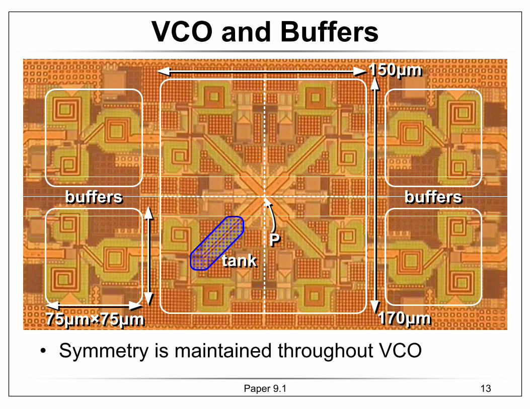
Paper 9.1 13
VCO and Buffers
• Symmetry is maintained throughout VCO
150μm
buffersbuffersbuffersbuffers
75μm×75μm75μm×75μm
150μm150μm
170μm170μm
PPtanktank

Paper 9.1 14
Frequency Divider
• Layout designed to minimize critical path delay
from VCO
out
22μm
100μm
200μm

Paper 9.1 15
Technology – 65nm GP CMOS
• fMAX=280GHz, fT=195GHz
• Device: 80×60nm×1μm, one side gate contact
• 7 metal backend, Metal-Over-Metal capacitors
0
50
100
150
200
250
300
0 0.2 0.4 0.6 0.8 1 1.2VDS (V)
f T, f
MA
X(G
Hz)
fMAX
fT
VGS=0.65V
50
100
150
200
250
300
0.1 1JDS (mA/μm)
f T, f
MA
X(G
Hz)
20.02
fMAX
fT
VDS=1V

Paper 9.1 16
Measured varactor at 94 GHz
• LG=60nm, Wtotal=27.5μm, CVAR’=1.53fF/μm2
• C variation: 25fF – 42fF, Q: 6 – 8 at 94 GHz
G SD
50 fingers
4
5
6
7
8
9
-0.6 -0.3 0 0.3 0.6 0.9 1.2VGS (V)
Q
20
25
30
35
40
45
CV
AR
(fF
)
CVAR
Q

Paper 9.1 17
S11
, S22
, S21
(dB
)Measured 24-µm 1:1 transformer
• Transformer:– VCO & Div– VCO & Mixer– LNA & Mixer
• MAG < -1.5dB
port 1
port 2 center tap
+ −
+ −
d
sw
d=24μmw=2μms=1μm

Paper 9.1 18
Receiver Die Photo
1095μm
600μ
m
Paper 9.1 19
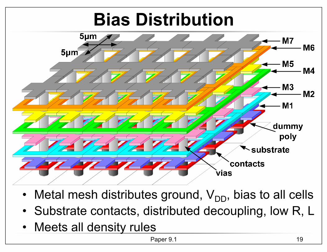
Bias Distribution
• Metal mesh distributes ground, VDD, bias to all cells• Substrate contacts, distributed decoupling, low R, L• Meets all density rules

Paper 9.1 20
Measurement Setup• SSB gain• Linearity• Phase
noise• Tuning
range• Divider
• DSB NF• DSB gain

Paper 9.1 21
DC Power Consumption
206.4 (158)Total:
19.616.3Divider 50-Ω driver
22.418.6Divider
28.8244 VCO buffers
57.6
1.2
48Quadrature VCO
28.51950-Ω IF amplifier
13.59Mixer
36
1.5
24LNA
Power (mW)Supply (V)Current (mA)Block

Paper 9.1 22
VCO Tuning & Output Power
VC
O F
req
uen
cy (
GH
z)
VC
O O
utp
ut
Po
wer
(d
Bm
)
• 88.2 – 91.2GHz tuning range for all temperatures• +3dBm to -4dBm total VCO output power

Paper 9.1 23
Measured VCO Phase Noise
• -95dBc/Hz at 1MHz offset• Measured at 90.3GHz• 100 averages

Paper 9.1 24
SSB Receiver Conversion Gain
-10
-5
0
5
10
15
75 80 85 90 95 100 105RF (GHz)
Dif
fere
nti
al G
ain
(d
B)
-35
-30
-25
-20
-15
-10
S11
(dB
)
Gain
S11
1.2V1.5V1.8VS11
• 12 dB differential gain with nominal bias• S11 better than -15 dB over the BW
VCO = 89GHz

Paper 9.1 25
Measured Receiver DSB NF
• 6 – 9.5 dB DSB NF• Gain confirmed by NF measurement
0
2
4
6
8
10
12
14
16
18
0 3 6 9 12 15 18IF (GHz)
Dif
fere
nti
al G
ain
(d
B)
4
6
8
10
12
14
16
18
20
22
DS
B N
F (
dB
)
NFGain
VCO = 89GHz

Paper 9.1 26
Measured Rx Optimal Bias
• Current swept in the 1st LNA stage
• JGAIN,OPT > JNFMIN,OPT , insensitive to VT, Ibias variation
1
3
5
7
9
11
13
15
0 0.1 0.2 0.3 0.4 0.5Current Density (mA/μm)
1
3
5
7
9
11
13
15
0 0.1 0.2 0.3 0.4 0.5Current Density (mA/μm)
25 °C50 °C75 °C
LO=89GHzIF = 6 GHz

Paper 9.1 27
Measured Receiver Linearity
• RF = 85 GHz, LO = 89 GHz• Input P1-dB = -18 dBm
Dif
fere
nti
al G
ain
(d
B)
Ou
tpu
t P
ow
er (
dB
m)

Paper 9.1 28
Measured Static Divider Operation
• Measured by observing the VCO and divider signals simultaneously
44
44.2
44.4
44.6
44.8
45
45.2
45.4
45.6
88 88.5 89 89.5 90 90.5 91VCO Frequency (GHz)
25 °C50 °C

Paper 9.1 29
Comparison to Previous Work: 60G
0.13μm CMOS0.13µm SiGe
BiCMOS65-nm GP CMOSTechnology
3.8 mm25.78 mm20.66 mm2Die Area
1.2V2.7 V1.2 V / 1.5 VSupply
76.8 mW527 mW206.4 mWDC Power
-93dBc/Hz (at 29GHz)
-90dBc/Hz-95 dBc/Hz (at
90.3GHz)VCO PN @ 1MHz off.
28.4-29.4GHz16.8-18.3GHz88.3-91.3GHzVCO Freq.
-15.8 dBm-36 dBm-18 dBmInput P1-dB
10.45-6.7 dB7 dBNF
11.8 dB38-40 dB12.5 dBPower Gain
57 – 63 GHz59 – 64 GHz76 – 95 GHz3-dB BW
VCO, doubler, LNA, mixer, IF amplifier
LNA, super-heterodyne receiver,
PLL, BB amp.
fundamental VCO, LNA, mixer, 50-Ω IF amp, static divider
Integration level
S. Emami, ISSCC07B. Floyd, ISSCC06This WorkSpec.

Paper 9.1 30
Comparison to Previous Work: 77G
250 fMAX SiGe HBT
6.46 mm2
3.3 / 5 V
186 mW
-95 dBc/Hz (at 54GHz)
52 GHz
-27.5 dBm
8-10 dB
35 dB
76 – 80 GHz
VCO, LNA, mixer, injection locked divider
Babakhani, ISSCC’06
230/300GHz fT/fMAX
0.13µm SiGe HBT65-nm GP CMOSTechnology
1.02 mm20.66 mm2Die Area
1.8 / 2.5 / 3.3 V1.2 V / 1.5 VSupply
700 mW206.4 mWDC Power
-99 dBc/Hz-95 dBc/Hz (at
90.3GHz)VCO PN @ 1MHz off.
76 GHz88.3-91.3GHzVCO Freq.
-30 dBm-18 dBmInput P1-dB
5.2 dB7 dBNF
31 dB12.5 dBPower Gain
85 – 96 GHz76 – 95 GHz3-dB BW
VCO, mixer, LNA, 50-Ω IF amplifier,
static ÷ 64
fundamental VCO, LNA, mixer, 50-Ω IF
amp, static ÷ 2
Integration level
Nicolson, MTT’08This WorkSpec.

Paper 9.1 31
Conclusion• 76-95GHz receiver with 90-GHz VCO and divider
• Clock distribution using transformers
• Unique bias distribution & isolation scheme
• Operation verified up to 100°C
• Highest-frequency CMOS receiver (for now)
• W-band receiver integration demonstrated

Paper 9.1 32
Acknowledgements• Alexander Tomkins for varactor measurements
• Kenneth Yau for transistor measurements
• STMicroelectronics for fabrication
• Christophe Garnier and Bernard Sautreuil for technology access
• NSERC for funding