Embed Size (px)
Citation preview

Background • Symetrix has strong history as IP provider
– > 25 years of development
– >200 U.S. and foreign patents.
– > $70M in research revenues, royalties and other income from development.
• Symetrix has licensed various technologies to eleven separate companies.
• Several of these technologies are in high volume production, most notably FeRAM at Panasonic.
Symetrix Corporation
1

Basic Idea of CeRAM Game Changer – No Filaments
• Control of material properties and proper device architecture are fundamental to this new paradigm. Evidence? No filament formation. (No electroforming)
• The CeRAM resistor is designed to exploit materials properties, surface properties, switching mechanism (endurance) and memory mechanism (retention).
• Optimizing CeRAM is a different science than building the perfect filament.
2

Baseline
The device is like a diode (varistor) to start with:
METAL TRANSITION
METAL OXIDE
METAL
The surfaces are defect-rich with oxygen vacancies, transition metal excess, grain boundaries…
And a schottky barier !! Su
rface
Surface
3

Baseline
METAL
TRANSITION METAL
OXIDE (TMO) METAL
CeRAM T M O
METAL METAL CONDUCTIVE
TMO CONDUCTIVE
TMO
60 nm
10 nm
ReRAM
Surface
Surface
Active Region
4

Why the Layers?
• Eliminate space charge at the interface
• Doping of TMO to make it conductive as-deposited (valence stabilization)
• Differential Doping to create active region that is “switchable” and repeatable (“pure” phase transition)
• Isolate and thin the active region where the “electronic switch” property can be used exclusively----what electronic switching property? (Next slide)
5

IV Characteristics - Device Physics
GD = DIFFUSIVE TRANSPORT – DRUDE GB = BALLISTIC TRANSPORT DUE TO e-e CHARGE GAP CLOSING IN THE TRANSITION METAL ION 3d ORBITALS GOFF= NO TRANSPORT IN INSULATING PHASE CONTROLLED BY e-e REPULSION IN 3d ORBITALS
VSET VRESET
?
BALLISTIC TRANSPORT
I = G D V I = G B V
I = G OFF V ~ 0
A
B
?
6

Underlying Physical Mechanism
VSET VRESET
? A
A Is a quantum phase transition • Mott, charge transfer (CT) but not Anderson • Extended band gap is of no consequence here • Only localized electron matters (in the atom) • Extremely high speed – 80 femtoseconds
7

B Needs to be thermionic emission only to be sharp and cohesive so that it matches the charge gap energy (no fluctuations)
Underlying Physical Mechanism
VSET VRESET
BALLISTIC TRANSPORT
B
?
VREAD
8

P
P
Mott Insulators
MOTT TYPE
DOS(E)
E
EF
dn+1
dn-1
EF U = UC U = 0
INSULATOR METAL
DOS(E)
dn
9

CHARGE TRANSFER “MOTT INSULATOR”
P
EF U = 0
METAL
DOS(E)
dn
P
DOS(E)
E
EF
dn+1
dn-1
INSULATOR
Δ
Mott Insulators
10

Charge Transfer M Mott Insulator
P
E
EF
dn+1
dn-1
INSULATOR
Δ
DOS(E)
11

A – FROM METAL TO INSULATOR PHASE TRANSITION B – FROM INSULATOR TO METAL PHASE TRANSITION
IV Characteristics - Device Physics
VSET VRESET
? I = GB V
A
B
?
12

The Switch
ELECTRON SEA (+) (-)
+
THE SWITCH IS HERE
• The density of states modulates the screening length λTF = ε0 / e2 DOS(EF)
• The screening length modulates the current J ≈ 1 / λTF
Metal Side
13

METAL
• Valence electrons screen the transition metal atom (ion)
• Narrows the potential well v(x) • Releases localized electron –
closes the gap
DOS
EF
Screening
14
METAL V V(X)
Releases localized electron. Metal.
Captures and localizes Electron – repulsive u Opens the gap. Insulator.
INSULATOR CHARGE GAP
Screening
15

Disproportionation
• A single atom can have oxidation and reduction reaction at the same time
• GAP = I – A I = ionization energy A = e- AFFINITY
For Nickel (Oxide) ---- d8 “splits” Into d7 and d9
U > 0
d7
d9
16

Switching
C((((
(+) ONTACT
(-) +
+
+
+
Electron deficient at reset
n(x) = n(critical)
This causes U to appear
SPEED OF PHASE TRANSITION IN FEMTOSECONDS
ELECTRON DRIFT VELOCITY IN NANOSECONDS
Active Region
17

KEY POINTS
• The robustness of device switching requires control of the nickel ion oxidation number, specifically the suppression of Ni+4 and Ni0 species that inhibit the pure Mott transition:
2Ni+2 Ni+1 + Ni+3
• This is achieved with ligand doping, specifically CO- .
• Co- doping stabilizes the CeRAM resistive element at Ni+2 and the NiO film is conductive as-deposited.
• There is no rupturing and reformation of filaments, there is no oxygen diffusion (Memristor), only a pure Mott (charge transfer) phase transition 18

Technology Highlights
• Low temperature processing ~400c
• Robust retention at 300-400 c - proved
• Reading at 0.2 volts 1012 times – proved
• Read memory widens with device scaling
• Variability reduced due to clean surfaces and isolated active region – proved
• Results demonstrated on 0.8µ devices only. Smaller feature sizes have been recently enabled under a program with Univesity of Texas at Dallas.
19
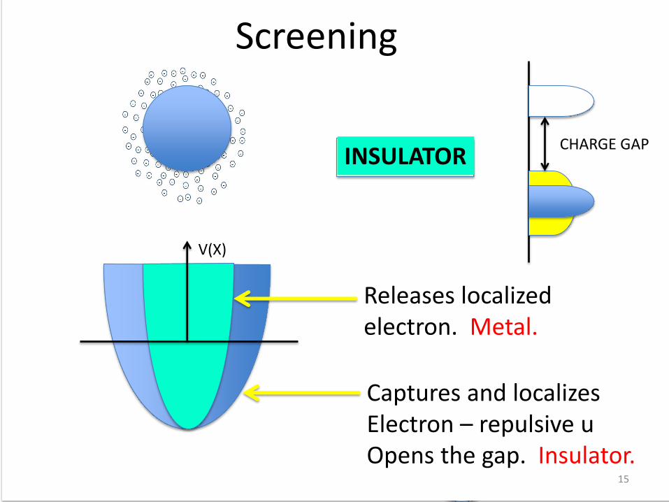
CeRAM STATUS
• THEORY: Confirmed with empirical results DONE
• MATERIALS: Doping any TMO with any extrinsic ligand PATENTED
• PROCESS: Create and isolate thin (5 nm) active region by simple spin-on or ALD PATENT FILED
• ARCHITECTURE: Array only (no pass gate) PATENTED
• 3-D (STACKING) With only silicon friendly materials IN PROCESS
• FPGA Architecture PATENT FILED
20

Implications
A NEW DEVICE AND THEORETICAL PARADIGM HAS BEEN DEVELOPED FOR RESISTIVE SWITCHING MEMORIES, ONE THAT:
• Eliminates the oxygen diffusion effect (basis of memristor) to allow “pure” Mott-like transition.
• Reduces variability in key parameters (vset & vreset) that has prevented ReRAM commercialization.
• Provides the robustness and repeatability required by future device scaling.
• Offers a path to 3d (stackable) memory architectures. • May, in time, replace transistors as the fundamental
switch in circuits. 21