Embed Size (px)
Citation preview
8/13/2019 A New Design Technique to Reduce the Ground Bounce Noise and Leakage in Four bit Binary Adder Circuit
http://slidepdf.com/reader/full/a-new-design-technique-to-reduce-the-ground-bounce-noise-and-leakage-in-four 1/8
ACEEE Int. J. on Signal and Image Processing , Vol. 4, No. 3, Sept 2013
© 2013 ACEEE
DOI: 01.IJSIP.4.3.
Full Paper
A New Design Technique to Reduce the Ground
Bounce Noise and Leakage in Four bit Binary Adder
CircuitShweta Singh1, Neelam arya2, Manisha Pattanaik 2
1ABVIIITM Gwalior, VLSI Group. E amil : [email protected] Gwalior, VLSI Group. E amil : [email protected], [email protected]
Abstract- The performance degradation with technology scaling
is one of the major issues in today’s life. Leakage power
dissipation in the IC increases exponentially with technology
continuously scaling down. Multi threshold CMOS Power
Gating is a very well known way to reduce leakage current,
but when circuit transition goes from sleep to active mode,
due to abrupt transitions introduces Ground Bounce Noise in
the circuit, it disturbs the normal working of any circuit and
tends to wrong output and also reduces the reliability of circuit.
In this paper two effective Power Gating techniques “Ultra
low power (ULP) diode based technique with parallel sleep
pMOS transistors” and “Single header ba sed Ultra Low Power
diode with parallel sleep pMOS transistors” are proposed.
These are dealing with Ground Bounce Noise and Leakage
problem in the circuit. For that an additional wait mode and
extra header transistor is added in the circuit to reduce the
ground bounce noise. A comparison analysis between existing
and proposed power gating techniques has been done on 90nm
technology node, which shows that the proposed techniques
“Ultra low power diode based technique with parallel sleep
pMOS transistors” and “Single header based ultra Low Power
diode with parallel sleep pMOs transistors” reduces leakage
by 70.40 and 70.70% respectively and ground bounce noise by
10.38, 14.02% respectively in comparison to Diode Based
trimode power gating technique..
Keywords-Ground Bounce Noise, Leakage current, Ultra Low
Power Diode, Body biasing
I. I NTRODUCTION
In advance CMOS technology with technology scaling
the supply voltage and the threshold voltage also continu-
ously scaling down, due to which leakage power dissipation
increases in the circuit, it is one of the biggest challenges
related to low power designs in today’s life. Multi threshold
CMOS Power Gating is an efficient technique to suppress
the Leakage current, and to reduce the Leakage Power in the
circuit in standby mode [1][2][16]. In this power gating tech-
nique, a High Threshold (High-Vth) transistor is added either
between Supply Rail and Logic block (Header) or Logic block
and Ground Rail (Footer), or a combination of both is used
[4]. MTCMOS Power Gating is a technique in which certain
part of the chip turned off, when chip is idle. At the same
time, during low Vth circuit mode transition from sleep mode
to active mode, power gated circuit suffers from ground
Bounce Current due to sudden discharge path from virtual
Vdd
to Ground line, as shown in Fig.1, which results from
parasitic inductance of circuit [3]. High Threshold voltage
for sleep transistor is chosen due to fact that it restricts the
leakage current and Logic block consists of low voltage tran-
sistors to increase the performance of the circuit.[7][9]
In Fig.1 drain of the high threshold nMOS sleep transistor
is at voltage H” Vdd
, when circuit is in standby mode the both
sleep transistor are turned off so low Vth block is disconnected
from supply and ground and leakage reduces, but when these
transistors switches from sleep mode to active mode, a surge
current flows due to discharge of the drain terminal of nMOS
sleep transistor, known as Ground Bounce Noise. Due to
Current surge produced during switching between sleep to
active mode MTCMOS Power Gating technique needs to
special attention to improve the reliability of the circuit.
Various MTCMOS techniques like tri-transistor controlled
MTCMOS, Dual switch MTCMOS, diode based trimode has
been proposed in past for reducing the leakage current in
standby mode and ground bounce noise (GBN) in sleep to
active mode transition of the circuit [8][13][15]. In various
power gating design uses the concept of extra wait state to
reduce the ground bounce noise [14]. In this paper different
multi threshold CMOS technique has been presented which
uses the concept of forward body biasing (FBB), reverse body biasing (RBB) and ultra low power diode. Ground
Bounce noise during mode transition of sleep to active and
leakage phenomena in standby mode is investigated in this
paper.
Organization of the paper is as follows: Diode based
trimode power gating is discussed in section II, different
proposed leakage reduction and ground bounce reduction
techniques are discussed in section III, comparison analysis
of different power gating techniques for leakage and ground
bounce noise with change in body bias voltage, supply
voltage, temperature and wait transistor resizing is discussed
in section IV, further reduction of ground bounce noise in
proposed design with body bias voltage and transistor resizing is discussed in section V, which is followed by
Conclusion in Section VI.
II. DIODE BASED TRIMODE TECHNIQUE
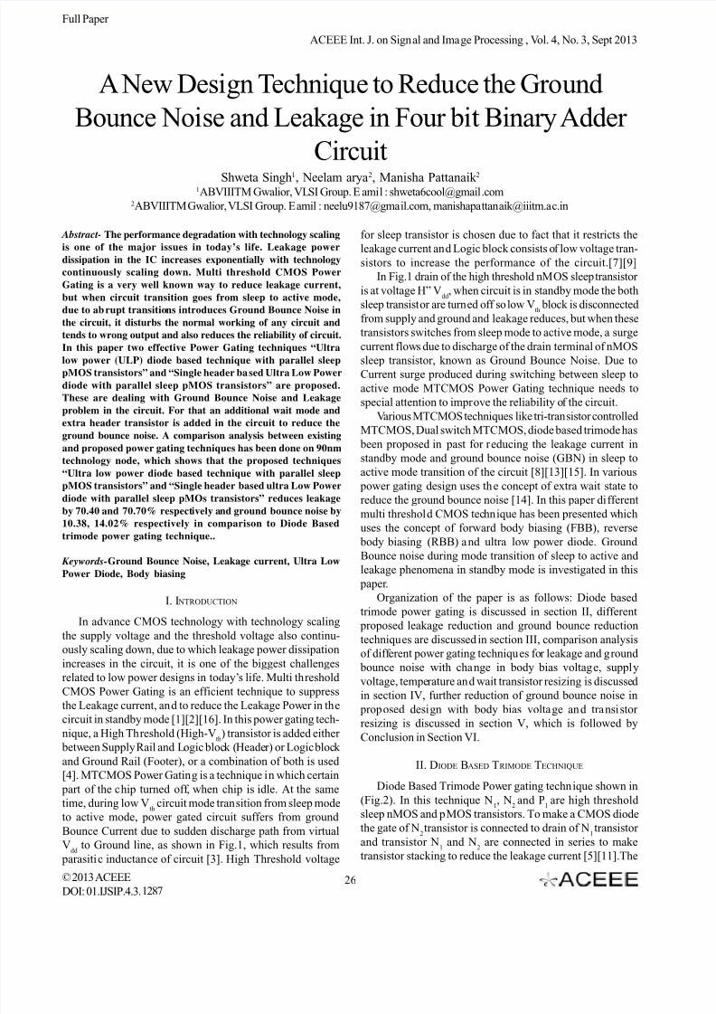
Diode Based Trimode Power gating technique shown in
(Fig.2). In this technique N1, N
2and P
1are high threshold
sleep nMOS and pMOS transistors. To make a CMOS diode
the gate of N2transistor is connected to drain of N
1transistor
and transistor N1 and N
2 are connected in series to make
transistor stacking to reduce the leakage current [5][11].The
1287
26
8/13/2019 A New Design Technique to Reduce the Ground Bounce Noise and Leakage in Four bit Binary Adder Circuit
http://slidepdf.com/reader/full/a-new-design-technique-to-reduce-the-ground-bounce-noise-and-leakage-in-four 2/8
© 2013 ACEEE
DOI: 01.IJSIP.4.3.
ACEEE Int. J. on Signal and Image Processing , Vol. 4, No. 3, Sept 2013
Full Paper
capacitor C1 is connected as shown in Fig.2 to control the
drain current of N1transistor and to control the intermediate
node voltage Vgnd2
. An additional wait mode is being intro-
duced between sleep to active mode transition of circuit by
adding an extra pMOS transistor P1in parallel [8]. Due to this
there are total three modes of operation sleep, wait and ac-
tive.
Fig.1 Power gating circuit
The sub threshold Leakage current expression is given
by equation (1). [5]
(1)
(2)
Vgs,V
bs and V
ds are the gate to source, bulk to source and
drain to source voltages respectively.Vth0
is the zero bias
threshold voltage, Cox
is the gate oxide capacitance and μn is
mobility. η is the drain induced barrier lowering coefficient
(DIBL) and γ is the body effect coefficient. Equation (1) and
(2) shows leakage current reduces exponentially when drainto source voltage decreases and if body effect increases
(negative V bs
).
When low threshold voltage adder circuit is in standby
mode all high threshold sleep nMOS and pMOS transistors
N1, N
2 and P
1 are turned off, due to this low V
thcircuit
disconnected from supply and ground and leakage current
reduces. At the same time intermediate node Vgnd2
is charged
up to some positive potential due to some small drain current
of sleep nMOS transistor N1, the drain-to source potential
Vds1
of sleep transistor N1 reduces due to this intermediate
node voltage Vgnd2
, It causes less drain induced barrier
lowering effect and negative body-to-source voltage V bs1
of
sleep transistor N1 leads to body effect. In this way stacking
of transistor reduces sub threshold leakage in the circuit.
The transistor N2 is diode connected, when this diode is
reverse biased, the source is seemed to be connected at gate,
so drain to source voltage Vds
of transistor N2 reduces and
due to this reduction in Vds
of transistor N2the leakage current
also reduces.
When circuit transition takes place from sleep to wait
mode the sleep transistor P1 turns on, but at the same time
transistor N1and N
2are in cut-off state. Forward body bias-
ing is used on wait transistor P1, due to which virtual ground
Vgnd1
discharges up to threshold voltage of P1 transistor eas-
ily without increasing the width of transistor and the first
peak of ground bounce noise, coming across it, will increase.
To complete the reactivation cycle, transition of circuit goes
from wait to active mode in which sleep transistor P1turns off
and transistors N1and N
2are turned on subsequently. By
controlling the drain to source voltage of transistor N2 and
intermediate node voltage Vgnd2 the ground bounce noise can be controlled more effectively. In wait to active mode transi-
tion the transistor N1 turns on first, at this moment the ca-
pacitance C1starts charging. When the capacitor C
1is charged
up to the threshold value of transistor N2 the transistor N
2
turns on and capacitor C1 starts discharging. Hence the
ground bounce noise reduces.
Fig.2. Diode Based trimode technique
III. PROPOSED TECHNIQUES
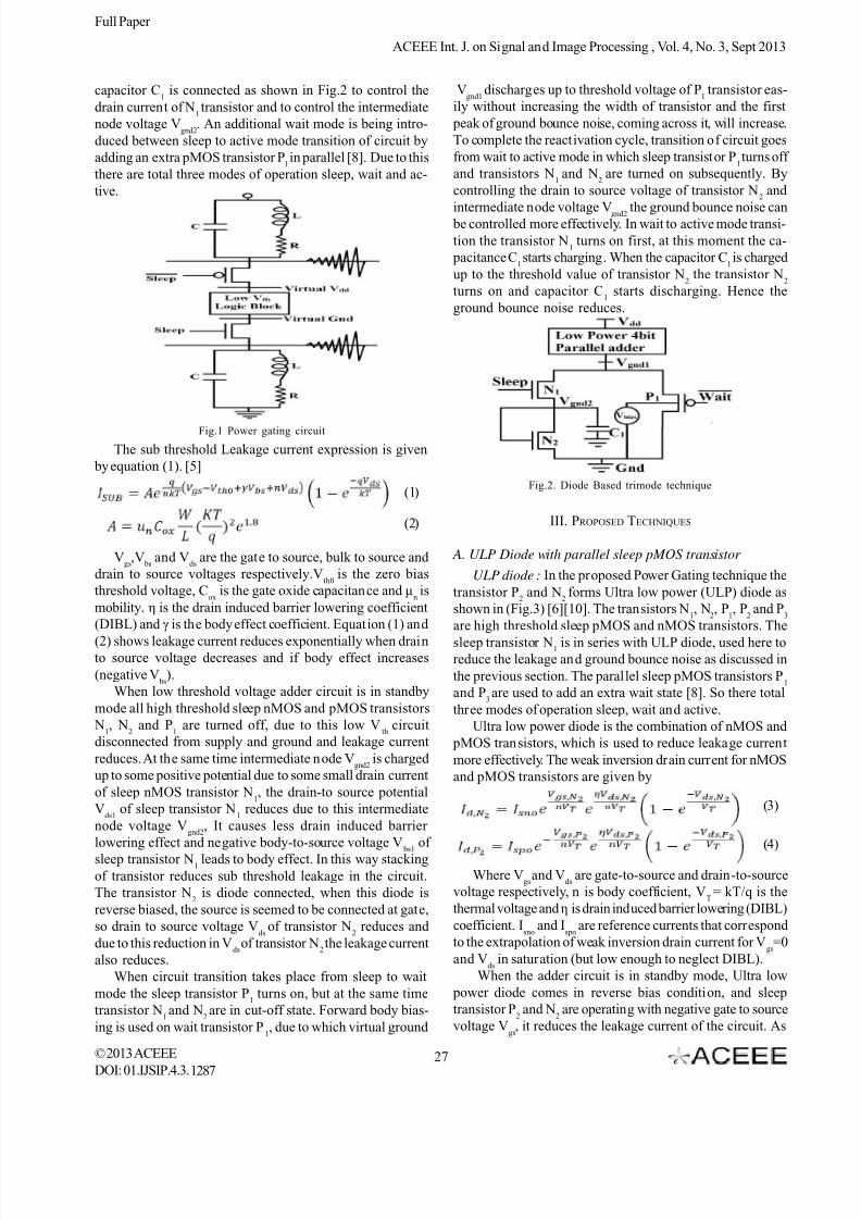
A. ULP Diode with parallel sleep pMOS transistor
ULP diode : In the proposed Power Gating technique the
transistor P2 and N
2forms Ultra low power (ULP) diode as
shown in (Fig.3) [6][10]. The transistors N1, N
2, P
1, P
2 and P
3
are high threshold sleep pMOS and nMOS transistors. The
sleep transistor N1 is in series with ULP diode, used here toreduce the leakage and ground bounce noise as discussed in
the previous section. The parallel sleep pMOS transistors P1
and P3are used to add an extra wait state [8]. So there total
three modes of operation sleep, wait and active.
Ultra low power diode is the combination of nMOS and
pMOS transistors, which is used to reduce leakage current
more effectively. The weak inversion drain current for nMOS
and pMOS transistors are given by
(3)
(4)
Where Vgs
and Vds
are gate-to-source and drain-to-source
voltage respectively, n is body coefficient, VT= kT/q is the
thermal voltage and η is drain induced barrier lowering (DIBL)
coefficient. Isno
and Ispo
are reference currents that correspond
to the extrapolation of weak inversion drain current for Vgs=0
and Vds in saturation (but low enough to neglect DIBL).
When the adder circuit is in standby mode, Ultra low
power diode comes in reverse bias condition, and sleep
transistor P2 and N
2 are operating with negative gate to source
voltage Vgs, it reduces the leakage current of the circuit. As
1287
27
8/13/2019 A New Design Technique to Reduce the Ground Bounce Noise and Leakage in Four bit Binary Adder Circuit
http://slidepdf.com/reader/full/a-new-design-technique-to-reduce-the-ground-bounce-noise-and-leakage-in-four 3/8
ACEEE Int. J. on Signal and Image Processing , Vol. 4, No. 3, Sept 2013
© 2013 ACEEE
DOI: 01.IJSIP.4.3.
Full Paper
given in equation (1) and (2) the leakage current is directly
proportional to transistor width , if width (W) of transistor
decrease, leakage also reduces. In proposed design uses two
parallel wait sleep pMOS transistors P1 and P
3, the width (W)
of transistors P1and P
3, shown in (Fig.3) is half of the width
of the transistor P1 of (Fig.2). So by decreasing the W of
transistor the leakage reduces here more effectively. To further
reduce the Leakage current uses reverse body biasing onsleep pMOS transistors in standby mode. It increases the
threshold voltage of the transistors, so leakage of the circuit
reduces.
When low Vth circuit transition takes place from sleep to
active mode, it will go from sleep to wait mode, at this time
transistor P3 turns on but sleep transistors N
1, N
2, P
1 and P
2
are turned off, at the same time virtual ground voltage Vgnd1
discharges through P3 up to the threshold voltage V
tp3 of
sleep transistor P3. The first peak of ground bounce noise
comes across it. The virtual ground voltage can be discharged
easily by using forward body biasing (FBB) on sleep transis-
tor P3without increasing the size of wait transistor [12]. After
a small time second wait transistor P1 turns on and forward body biasing is applied on it so again virtual ground voltage
is discharged through it up to the amount of threshold volt-
age Vtp1
of transistor P1and a second peak of ground bounce
comes across it. The virtual ground can be discharged easily
by using Forward body biasing on P1and P
3 sleep transis-
tors. To complete the reactivation process the circuit goes
from wait to active mode and transistor P1and P
3 turns off
and transistor N1 turns on, due to which capacitor C
1 starts
charging. When capacitor is charged up to the threshold
voltage of transistor N2, the transistor N
2 turns on and ca-
pacitor C1 starts discharging. In this way the use of transis-
tor stacking, ultra low power diode and parallel pMOS sleep
transistor ’P3’ and body biasing reduces the Ground bouncenoise to a considerable amount.
Fig.3. ULP Diode with parallel sleep pMOS transistor
Proposed design
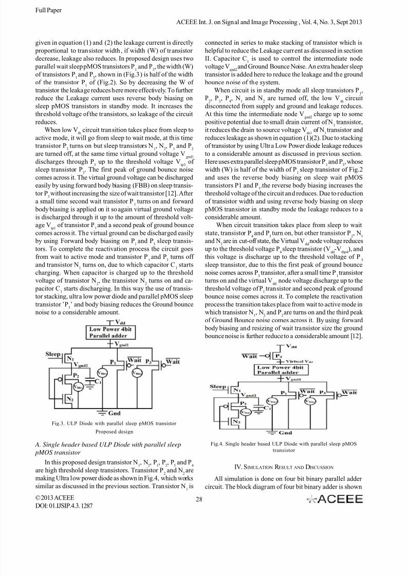
A. Single header based ULP Diode with parallel sleep
pMOS transistor
In this proposed design transistor N1, N
2, P
1, P
2, P
3 and P
4
are high threshold sleep transistors. Transistor P2 and N
2are
making Ultra low power diode as shown in Fig.4, which works
similar as discussed in the previous section. Transistor N1 is
connected in series to make stacking of transistor which is
helpful to reduce the Leakage current as discussed in section
II. Capacitor C1 is used to control the intermediate node
voltage Vgnd2
and Ground Bounce Noise. An extra header sleep
transistor is added here to reduce the leakage and the ground
bounce noise of the system.
When circuit is in standby mode all sleep transistors P1,
P2, P3, P4, N1 and N2 are turned off, the low V th circuitdisconnected from supply and ground and leakage reduces.
At this time the intermediate node Vgnd2
charge up to some
positive potential due to small drain current of N1 transistor,
it reduces the drain to source voltage Vds1
of N1transistor and
reduces leakage as shown in equation (1)(2). Due to stacking
of transistor by using Ultra Low Power diode leakage reduces
to a considerable amount as discussed in previous section.
Here uses extra parallel sleep pMOS transistor P1and P
3, whose
width (W) is half of the width of P1sleep transistor of Fig.2
and uses the reverse body biasing on sleep wait pMOS
transistors P1 and P3.the reverse body biasing increases the
threshold voltage of the circuit and reduces. Due to reduction
of transistor width and using reverse body biasing on sleep pMOS transistor in standby mode the leakage reduces to a
considerable amount.
When circuit transition takes place from sleep to wait
state, transistor P4and P
3turn on, but other transistor P
2, N
1
and N2are in cut-off state, the Virtual V
ddnode voltage reduces
up to the threshold voltage P4sleep transistor (V
dd -V
thp4), and
this voltage is discharge up to the threshold voltage of P3
sleep transistor, due to this the first peak of ground bounce
noise comes across P3 transistor, after a small time P
1transistor
turns on and the virtual Vdd
node voltage discharge up to the
threshold voltage of P1transistor and second peak of ground
bounce noise comes across it. To complete the reactivation
process the transition takes place from wait to active mode inwhich transistor N
1, N
2 and P
2are turns on and the third peak
of Ground Bounce noise comes across it. By using forward
body biasing and resizing of wait transistor size the ground
bounce noise is further reduce to a considerable amount [12].
Fig.4. Single header based ULP Diode with parallel sleep pMOS
transistor
IV. SIMULATION R ESULT AND DISCUSSION
All simulation is done on four bit binary parallel adder
circuit. The block diagram of four bit binary adder is shown
1287
28
8/13/2019 A New Design Technique to Reduce the Ground Bounce Noise and Leakage in Four bit Binary Adder Circuit
http://slidepdf.com/reader/full/a-new-design-technique-to-reduce-the-ground-bounce-noise-and-leakage-in-four 4/8
© 2013 ACEEE
DOI: 01.IJSIP.4.3.
ACEEE Int. J. on Signal and Image Processing , Vol. 4, No. 3, Sept 2013
Full Paper
in Fig.5. The basic circuit diagram of one bit full adder is
shown in Fig.6.
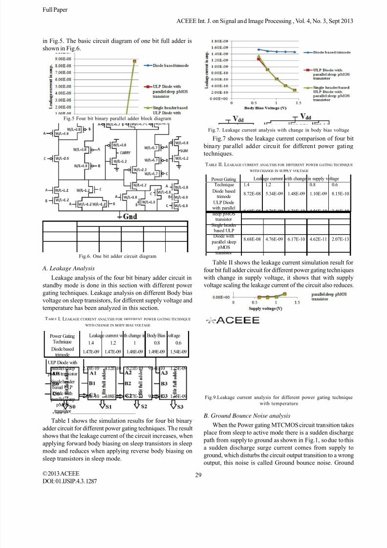
Fig.5 Four bit binary parallel adder block diagram
Fig.6. One bit adder circuit diagram
A. Leakage Analysis
Leakage analysis of the four bit binary adder circuit in
standby mode is done in this section with different power gating techniques. Leakage analysis on different Body bias
voltage on sleep transistors, for different supply voltage and
temperature has been analyzed in this section.
TABLE I. LEAKAGE CURRENT ANALYSIS FOR DIFFERENT POWER GATING TECHNIQUE
WITH CHANGE IN BODY BIAS VOLTAGE
Power GatingTechnique
Leakage current with change in Body Bias voltage
1.4 1.2 1 0.8 0.6
Diode basedtrimode
1.47E-09 1.47E-09 1.48E-09 1.49E-09 1.54E-09
ULP Diode with parallel sleep
pMOS transistor2.73E-10 4.12E-10 6.21E-10 9.14E-10 1.25E-09
Single header based ULP
Diode with parallel sleep
pMOS
transistor
2.68E-10 4.08E-10 6.17E-10 9.11E-10 1.35E-09
Table I shows the simulation results for four bit binary
adder circuit for different power gating techniques. The result
shows that the leakage current of the circuit increases, when
applying forward body biasing on sleep transistors in sleep
mode and reduces when applying reverse body biasing on
sleep transistors in sleep mode.
Fig.7. Leakage current analysis with change in body bias voltage
Fig.7 shows the leakage current comparison of four bit
binary parallel adder circuit for different power gating
techniques.
TABLE II. LEAKAGE CURRENT ANALYSIS FOR DIFFERENT POWER GATING TECHNIQUE
WITH CHANGE IN SUPPLY VOLTAGE
Power GatingTechnique
Leakage current with change in supply voltage
1.4 1.2 1 0.8 0.6
Diode basedtrimode
8.72E-08 5.34E-09 1.48E-09 1.10E-09 8.15E-10
ULP Diodewith parallel
sleep pMOStransistor
8.68E-08 4.76E-09 6.21E-10 4.56E-10 3.46E-10
Single header based ULPDiode with
parallel sleep pMOStransistor
8.68E-08 4.76E-09 6.17E-10 4.62E-11 2.07E-13
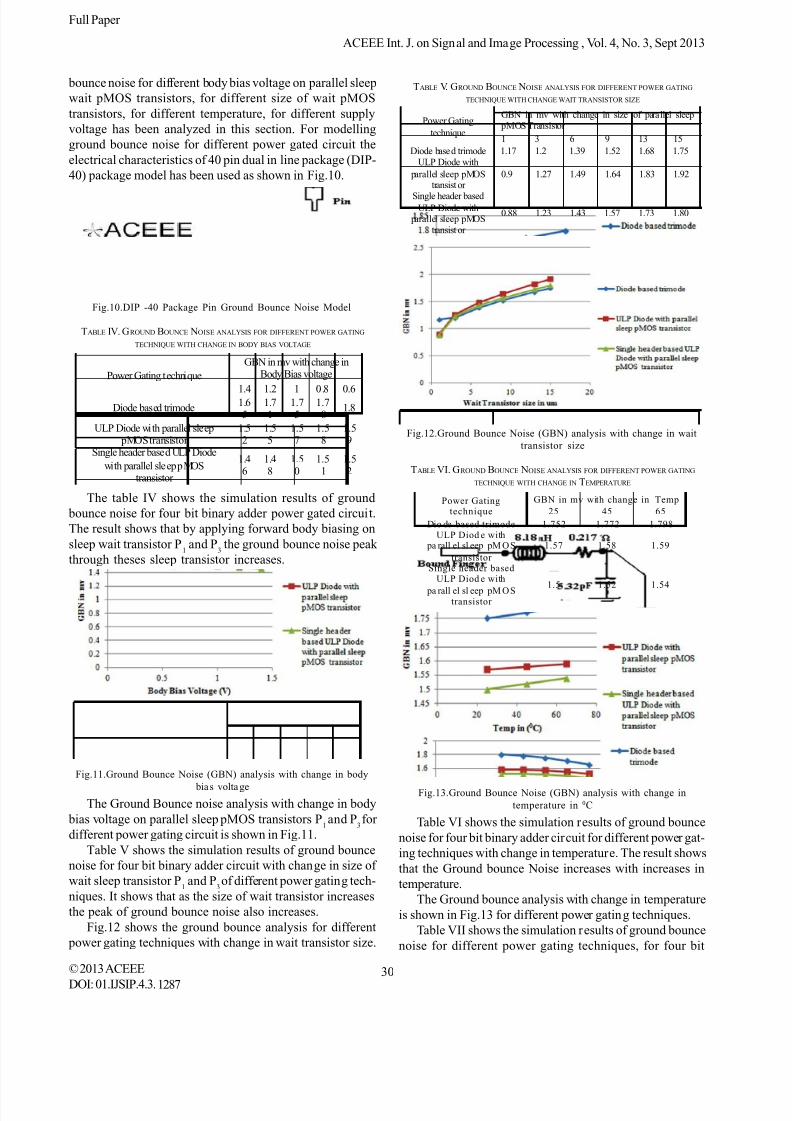
Table II shows the leakage current simulation result for
four bit full adder circuit for different power gating techniques
with change in supply voltage, it shows that with supply
voltage scaling the leakage current of the circuit also reduces.
Fig.9.Leakage current analysis for different power gating technique
with temperature
B. Ground Bounce Noise analysis
When the Power gating MTCMOS circuit transition takes
place from sleep to active mode there is a sudden discharge
path from supply to ground as shown in Fig.1, so due to this
a sudden discharge surge current comes from supply to
ground, which disturbs the circuit output transition to a wrong
output, this noise is called Ground bounce noise. Ground
1287
29
8/13/2019 A New Design Technique to Reduce the Ground Bounce Noise and Leakage in Four bit Binary Adder Circuit
http://slidepdf.com/reader/full/a-new-design-technique-to-reduce-the-ground-bounce-noise-and-leakage-in-four 5/8
ACEEE Int. J. on Signal and Image Processing , Vol. 4, No. 3, Sept 2013
© 2013 ACEEE
DOI: 01.IJSIP.4.3.
Full Paper
bounce noise for different body bias voltage on parallel sleep
wait pMOS transistors, for different size of wait pMOS
transistors, for different temperature, for different supply
voltage has been analyzed in this section. For modelling
ground bounce noise for different power gated circuit the
electrical characteristics of 40 pin dual in line package (DIP-
40) package model has been used as shown in Fig.10.
Fig.10.DIP -40 Package Pin Ground Bounce Noise Model
TABLE IV. GROUND BOUNCE NOISE ANALYSIS FOR DIFFERENT POWER GATING
TECHNIQUE WITH CHANGE IN BODY BIAS VOLTAGE
Power Gating technique
GBN in mv with change inBody Bias voltage
1.4 1.2 1 0.8 0.6Diode based trimode
1.65
1.71
1.75
1.78
1.8
ULP Diode with parallel sleep pMOS transistor
1.52
1.55
1.57
1.58
1.59
Single header based ULP Diode
with parallel sleep pMOStransistor
1.46
1.48
1.50
1.51
1.52
The table IV shows the simulation results of ground
bounce noise for four bit binary adder power gated circuit.
The result shows that by applying forward body biasing on
sleep wait transistor P1 and P
3 the ground bounce noise peak
through theses sleep transistor increases.
Fig.11.Ground Bounce Noise (GBN) analysis with change in body
bias voltage
The Ground Bounce noise analysis with change in body
bias voltage on parallel sleep pMOS transistors P1and P
3for
different power gating circuit is shown in Fig.11.
Table V shows the simulation results of ground bounce
noise for four bit binary adder circuit with change in size of
wait sleep transistor P1 and P
3of different power gating tech-
niques. It shows that as the size of wait transistor increases
the peak of ground bounce noise also increases.
Fig.12 shows the ground bounce analysis for different
power gating techniques with change in wait transistor size.
TABLE V. GROUND BOUNCE NOISE ANALYSIS FOR DIFFERENT POWER GATING
TECHNIQUE WITH CHANGE WAIT TRANSISTOR SIZE
Power Gating
technique
GBN in mv with change in size of parallel sleep pMOS Transistor
1 3 6 9 13 15
Diode based trimode 1.17 1.2 1.39 1.52 1.68 1.75
ULP Diode with
parallel sleep pMOStransist or
0.9 1.27 1.49 1.64 1.83 1.92
Single header basedULP Diode with
parallel sleep pMOS
transist or
0.88 1.23 1.43 1.57 1.73 1.80
Fig.12.Ground Bounce Noise (GBN) analysis with change in wait
transistor size
TABLE VI. GROUND BOUNCE NOISE ANALYSIS FOR DIFFERENT POWER GATING
TECHNIQUE WITH CHANGE IN TEMPERATURE
Power Gatingtechnique
GBN in mv with change in Temp
25 45 65
Dio de based trimode 1.752 1.772 1.798ULP Diod e with
pa rall el sl eep pM OS
transistor
1.57 1.58 1.59
Single header basedULP Diod e with
pa rall el sl eep pM OStransistor
1.5 1.52 1.54
Fig.13.Ground Bounce Noise (GBN) analysis with change in
temperature in 0C
Table VI shows the simulation results of ground bounce
noise for four bit binary adder circuit for different power gat-
ing techniques with change in temperature. The result shows
that the Ground bounce Noise increases with increases in
temperature.
The Ground bounce analysis with change in temperature
is shown in Fig.13 for different power gating techniques.
Table VII shows the simulation results of ground bounce
noise for different power gating techniques, for four bit
1287
30
8/13/2019 A New Design Technique to Reduce the Ground Bounce Noise and Leakage in Four bit Binary Adder Circuit
http://slidepdf.com/reader/full/a-new-design-technique-to-reduce-the-ground-bounce-noise-and-leakage-in-four 6/8
© 2013 ACEEE
DOI: 01.IJSIP.4.3.
ACEEE Int. J. on Signal and Image Processing , Vol. 4, No. 3, Sept 2013
Full Paper
binary parallel adder circuit with change in supply voltage.
The simulation results on the four bit binary power gating
adder circuit shows that the ground bounce noise of the
circuit increases with increases in supply voltage and de-
creases with reduction in supply voltage.
TABLE VII. GROUND BOUNCE NOISE ANALYSIS FOR DIFFERENT POWER GATING
TECHNIQUE WITH CHANGE IN SUPPLY VOLTAGE
Power Gatingtechnique
GBN i n mv with change in supply voltage1.4 1.2 1 0.8 0.6
Diode basedtrimode 1.88 1.84 1.75 1.16 0.71
ULP Diode with
parallel sleep
pMOS transistor 2.08 1.85 1.57 1.17 0.66Single he ader
base d ULP D iodewith parallel sleep pMOS transi stor 2.03 1.58 1.50 0.53 0.35
Fig.14.Ground Bounce Noise (GBN) analysis with change in supply
voltage
The ground bounce noise analysis with change in supply
voltage is shown in Fig.14.
V. FURTHER R EDUCTION OF GROUND BOUNCE
By applying FBB and transistor resizing on “single header
based ultra low power diode with para llel sleep pMOS
transistor” the ground bounce noise can be further reduced
[17][18].
When the wait transistor size of P1=7.5um and P
3=7.5 um
and body bias voltage is 1V in “Single header based Ultra
Low Power diode with parallel sleep pMOS transistor” the
first, second peak (during sleep to wait mode transition) and
third peak (during wait to active mode transition) of ground
bounce noise is shown in Fig.15 and voltage corresponding
to the peak are 1.505mv, 1.3525mv and 1.1126mv as shown in
table VIII.
To further reduce the peak of ground bounce noise
applying forward body biasing (V b=0.8V) on sleep parallel
wait transistors P1 and P
3. In this way from sleep to wait mode
transition the first peak and the second peak voltage of
Ground bounce noise increases here as shown in Fig.16 and
corresponding values 1.5147mv and 1.4321mv, and the third
peak of ground bounce noise from wait to active mode
transition reduces up to the voltage 1.0957mv.
To further reduce the ground bounce noise, resizing the
wait transistor up to width of (P1=6um and P
3=6um). By
reducing the wait transistor size the peak of ground bounce
noise across it reduces as already discussed in section.
Which is shown in Fig.17, from sleep to wait mode transition
the first peak and the second peak of ground bounce noise
reduces up to 1.441mv and 1.3423mv respectively and the
third peak voltage reduces up to 1.08mv from wait to active
mode transition. To further reduction of ground bounce noise peak again resize the wait transistor size up to width of (P1=4um
and P3=4um), it will further reduce the ground bounce noise
first and second peak up to 1.33mv and 1.19mv during sleep
to wait mode transition and third peak up to1.058mv during
wait to active mode transition as shown in Fig.18 and table
VIII.
Table VIII. Ground Bounce Noise Peaks for different wait
transistors size and body bias voltage
Body biasVoltage
in V
Wait transistor sizePeaks of GBN in mv
Peak1 Peak2 Peak3
BB=1 W1=7.5um W2=7.5um 1.51 1.35 1.11BB=0.8 W1=7.5um W2=7.5um 1.51 1.43 1.09
BB=0.8 W1=6um W2=6um 1.44 1.34 1.08
BB=0.8 W1=4um W2=4um 1.33 1.19 1.06
BB=0.8 W1=1.4um W2=2.5um 1.03 1.03 1.03
Fig.15.Ground Bounce Noise analysis with wait transistor size
(WP1
=7.5um and WP3
=7.5um) and body bias voltage (V b=V
dd =1V)
Fig.16.Ground Bounce Noise analysis with wait transistor size
(WP1
=7.5um and WP3
=7.5um) and body bias voltage (V b=0.8V)
1287
31
8/13/2019 A New Design Technique to Reduce the Ground Bounce Noise and Leakage in Four bit Binary Adder Circuit
http://slidepdf.com/reader/full/a-new-design-technique-to-reduce-the-ground-bounce-noise-and-leakage-in-four 7/8
ACEEE Int. J. on Signal and Image Processing , Vol. 4, No. 3, Sept 2013
© 2013 ACEEE
DOI: 01.IJSIP.4.3.
Full Paper
To further reduce the peak of ground bounce noise try to
make such type of combination of wait transistor size so that
the all three peaks of ground bounce noise become equal in
amplitude as shown in Fig.19. In this case the Ground bounce
noise comes minimum in comparison to all other cases. For
this again resize the wait transistor size of P1and P
3up size of
(P1=1.4um and P
3=2.5um). At this combination of body bias-
ing and transistor size the all three peaks of ground bouncenoise from sleep to wait mode and wait to active mode transi-
tion of the circuit become equal in amplitude that is 1.0287mv.
Fig.17.Ground Bounce Noise analysis with wait transistor size
(WP1
=6um and WP3
=6um) and body bias voltage (V b=0.8V)
Fig.18.Ground Bounce Noise analysis with wait transistor size
(WP1
=4um and WP3
=4um) and body bias voltage (V b=0.8V)
Fig.19.Ground Bounce Noise analysis with wait transistor size
(WP1
=2.5um and WP3
=1.4um) and body bias voltage (V b=0.8V)
Fig.20.Ground Bounce Noise analysis with wait transistor size WP1
and WP3
and body bias voltage V b
Fig.20 shows the Ground bounce noise comparison for
first, second and third peaks. It shows that all peaks of ground
bounce noise become equal in amplitude at wait transistor
size WP1
=1.4um and WP3
=2.5um at 0.8V body bias voltage.
VI. CONCLUSION
Leakage current reduction in standby mode and Ground
bounce noise reduction during mode transition for diode
based trimode technique, Ultra Low Power diode with parallel
sleep pMOs transistor with body biasing and Single header
based Ultra Low Power diode with parallel sleep pMOs
transistor with body biasing has been evaluated in this paper.
Use of transistor stacking, forward body biasing, reverse
body biasing, ultra low power diode and wait transistor
resizing reduces ground bounce noise and leakage current
to a considerable amount. Effect of wait transistor resizing,temperature, body biasing on sleep transistor and supply
voltage on leakage and ground bounce noise have been
analyzed in this paper.
It has been observed that by using proposed design “Ultra
Low Power diode with parallel sleep pMOS transistor with
body biasing” and “Single header based Ultra Low Power
diode with parallel sleep pMOS transistor with body biasing”
Leakage can be reduces up to 70.40% and 70.70% respectively
by using reverse body biasing in comparison to Diode based
trimode technique and Ground bounce Noise can be reduced
by to 10.38% and 14.02% respectively in comparison to
“Diode based trimode technique”. With increment of
temperature and supply voltage the peaks of ground bounce
noise and leakage current increases. By reducing the wait
transistor size the ground bounce noise peak further reduces.
ACKNOWLEDGEMENT
As an author I wish to thank Dr. Manisha Pattanaik for
her constant support and motivation as a guide and as a
mentor. I also wish to appreciate Neelam arya for her support
and help during the tenure of this research. This work was
supported by the VLSI research group of ABV-IIITM, Gwalior.
1287
32
8/13/2019 A New Design Technique to Reduce the Ground Bounce Noise and Leakage in Four bit Binary Adder Circuit
http://slidepdf.com/reader/full/a-new-design-technique-to-reduce-the-ground-bounce-noise-and-leakage-in-four 8/8
© 2013 ACEEE
DOI: 01.IJSIP.4.3.
ACEEE Int. J. on Signal and Image Processing , Vol. 4, No. 3, Sept 2013
Full Paper
R EFERENCES
[1] Singh, H.; Agarwal, K.; Sylvester, D.; Nowka, K.J., “Enhanced
Leakage Reduction Techniques Using Intermediate Strength
Power Gating,” Very Large Scale Integration (VLSI) Systems,
IEEE Transactions on , vol.15, no.11, pp.1215,1224, Nov.
2007
[2] S.G. Narendra and A. Chandrakasan, Leakage in Nanometer
CMOS Technologies. New York: Springer-verlag, 2006
[3] Suhwan Kim; Kosonocky, S.V.; Knebel, D.R., “Understanding
and minimizing ground bounce during mode transition of power
gating structures,” Low Power Electronics and Design, 2003.
ISLPED ’03. Proceedings of the 2003 International
Symposium on , vol., no., pp.22,25, 25-27 Aug. 2003
[4] Gautam, M.; Akashe, S., “Reduction of leakage current and
powe r in fu ll subtractor using MT CMO S tech niqu e,”
Computer Communication and Informatics (ICCCI), 2013
International Conference on , vol., no., pp.1,4, 4-6 Jan. 2013
[5] Bhanuprakash, R.; Pattanaik, M.; Rajput, S.S.; Mazumdar, K.,
“Analysis and reduction of ground bounce noise and leakage
current during mode transition of stacking power gating logic
circuits,” TENCON 2009 - 2009 IEEE Region 10 Conference
, vol., no., pp.1,6, 23-26 Jan. 2009
[6] Levacq, D.; Dessard, V.; Flandre, D.; , “Low Leakage SOI
CMOS Static Memory Cell With Ultra-Low Power Diode,”
Solid-State Circuits, IEEE Journal of , vol.42, no.3, pp.689-
702, March 2007
[7] Rani, M. Janaki; Malarkkan, S., “Leakage power reduction in
CMOS modulo4 adder and modulo4 multiplier in sub-micron
technology,” Sustainable Energy and Intelligent Systems
(SEISCON 2011), International Conference on , vol., no.,
pp.593,597, 20-22 July 2011
[8] Hailong Jiao; Kursun, V., “Ground bouncing noise suppression
techniques for MTCMOS circuits,” Quality Electronic Design,
2009. ASQED 2009. 1st Asia Symposium on , vol., no.,
pp.64,70, 15-16 July 2009
[9] Pattanaik, M.; Agnihotri, S.; Varaprashad, M.V.D.L.; Arasu,
T.A., “Enhanced Ground Bounce Noise Reduction in a LowLeakage 90nm 1-Volt CMOS Full Adder Cell,” Electronic
System Design (ISED), 2010 International Symposium on,
vol., no., pp.175,180, 20-22 Dec. 2010.
[10] Flandre, D.; Bulteel, O.; Gosset, G.; Rue, B.; Bol, D.; , “Ultra-
low-power analog and digital circuits and microsystems using
disruptive ultra-low-leakage design techniques,” Devices,
Circuits and Systems (ICCDCS), 2012 8th International
Caribbean Conference on , vol., no., pp.1-2, 14-17 March
2012.
[11] Manisha Pattanaik, Balwinder Raj, Shashikant Sharma and
Anjan Kumar,” Diode Based Trimode Multi-Threshold CMOS
Technique for Ground Bounce Noise Reduction in StaticCMOS Adders ”, International Conference on Electronics,
Nanomaterials and Components, Advanced Materials Research
, Vol. 548, pp. 885-889, China 2012
[12] Hailong Jiao; Kursun, V., “Sleep transistor forward body bias:
An Extra Knob to lower ground bouncing noise in MTCMOS
circuits,” SoC Design Conference (ISOCC), 2009 International
, vol., no., pp.216,219, 22-24 Nov. 2009
[13] Hailong Jiao; Kursun, V., “Ground Bouncing Noise Suppression
Techniques for Data Preserving Sequential MTCMOS
Circuits,” Very Large Scale Integration (VLSI) Systems, IEEE
Transactions on , vol.19, no.5, pp.763,773, May 2011
[14] Suhwan Kim; Kosonocky, S.V.; Knebel, D.R.; Stawiasz, K.;
Papaefthymiou, M.C., “A Multi-Mode Power Gating
Structure for Low-Voltage Deep-Submicron CMOS ICs,”Circuits and Systems II: Express Briefs, IEEE Transactions
on , vol.54, no.7, pp.586,590, July 2007
[15] Hailong Jiao; Kursun, V., “Ground-Bouncing-Noise-Aware
Combinational MTCMOS Circuits,” Circuits and Systems I:
Regular Papers, IEEE Transactions on , vol.57, no.8,
pp.2053,2065, Aug. 2010
[16] Neema, V.; Chouhan, S.S.; Sanjiv Tokekar, “VSECURE: Active
& standby subthreshold leakage current reduction technique,”
Microelectronics (ICM), 2010 International Conference on ,
vol., no., pp.68,71, 19-22 Dec. 2010
[17] Hailong Jiao; Kursun, V., “How forward body bias helps to
reduce ground bouncing noise and silicon area in MTCMOS
circuits: Divulging the basic mechanism,” SoC Design
Conference (ISOCC), 2010 International , vol., no., pp.9,12,22-23 Nov. 2010
[18] Hailong Jiao; Kursun, V., “Dynamic forward body bias enhanced
tri-mode MTCMOS,” Quality Electronic Design (ASQED),
2010 2nd Asia Symposium on , vol., no., pp.33,37, 3-4 Aug.
2010
1287
33